1 Design Validation and Debugging Tim Cheng Department of Electrical & Computer Engineering UC Santa Barbara VLSI Design and Education Center (VDEC) Univ. of Tokyo

1 Design Validation and Debugging Tim Cheng Department of Electrical & Computer Engineering UC Santa Barbara VLSI Design and Education Center (VDEC) Univ.
Dec 22, 2015
Welcome message from author
This document is posted to help you gain knowledge. Please leave a comment to let me know what you think about it! Share it to your friends and learn new things together.
Transcript

1
Design Validation and Debugging
Tim Cheng
Department of Electrical & Computer Engineering
UC Santa Barbara
VLSI Design and Education Center (VDEC)Univ. of Tokyo

2
Harder to Design Robust and Reliable Chips• First-silicon success rate has been dropping
– ~30% for complex ASIC/[email protected] (according to an ASIC vendor)
– Pre-silicon logic bugs have been increasing at 3X-4X per generation for Intel’s processors
• Yield has been dropping for volume production and takes longer to ramp up the yield– IBM’s 8-core Cell-Processor chips: ~10-20% yield (July
2006)
• “Better than worst-case” design resulting in failures w/o defects– Increase in variation of process parameters with scaling
– Worst-case design getting way too conservative

3
In-Field Failures are Common and Costly
• Xbox:16.4% failure rate
• Additional warranty and refund will cost Microsoft $1.15B ($86 per $300-item)
• More than financial cost: reputation and market loss
• Non-trivial failure rate
– 15% in average
http://arstechnica.com/news.ars/post/20080214-xbox-360-failure-rates-worse-than-most-consumer-electornics.html

4
Design for Robustness and Reliability
• Systems must be designed to cope with failures • Efficient silicon debug is becoming a must
– Need efficient design validation and debugging methodology
– Design for debugging would become necessary
• Must have embedded self-test for error detection – For both testing in manufacturing line and in-field testing– Both on-line and off-line testing
• Re-configurability and adaptability for error recovery make better sense– Using spares to replace defective parts– Using redundancy to mask errors– Using tuning to compensate variations
5
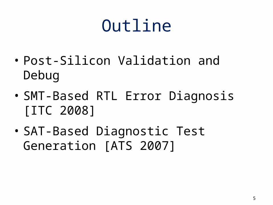
Outline
• Post-Silicon Validation and Debug
• SMT-Based RTL Error Diagnosis [ITC 2008]
• SAT-Based Diagnostic Test Generation [ATS 2007]

6
Bugs in Silicon• Manufacturing defects
– Discovered during manufacturing test (<<1M DPM)
• Functional bugs (AKA logic bugs)– Exist in all components
– ~98% found before tape out, ~2% post-silicon*
• Circuit bugs (AKA electrical bugs)– Not all components exhibit failures
– Fails in some operating region (voltage, temperature, or frequency)
– Usually cause by design margin errors, IR drop, crosstalk coupling, L di/dt noise, process variation …
– ~50% found before tape out, ~50% post-silicon*
* Source: Intel

7
Validation Domain Characteristics
• Pre-silicon validation– Cycle accurate simulation
– FSIM << FPROD: cycle poor
– Any signal visible (i.e. white box): debugging is straightforward
– Limited platform level interaction
• Post-silicon validation– Tests run at FPROD: cycle rich
– Component tested in platform configuration– Only package pins visible: difficult debug
8
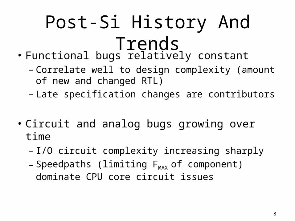
Post-Si History And Trends
• Functional bugs relatively constant– Correlate well to design complexity (amount
of new and changed RTL)– Late specification changes are contributors
• Circuit and analog bugs growing over time– I/O circuit complexity increasing sharply
– Speedpaths (limiting FMAX of component) dominate CPU core circuit issues

9
Post-Si Debug Challenges
• Trend is toward lower observability– Integration increasing towards SoC
• Functional and circuit issues require different solutions
• On average circuit bugs take 3x as much time to root cause vs. functional bugs– Bugs found on platforms, but are debugged on debug-
enabled automatic test equipment (ATE)
– Often need multiple iterations to reproduce on the tester
– Often long latency between circuit issue and it’s syndrome
10
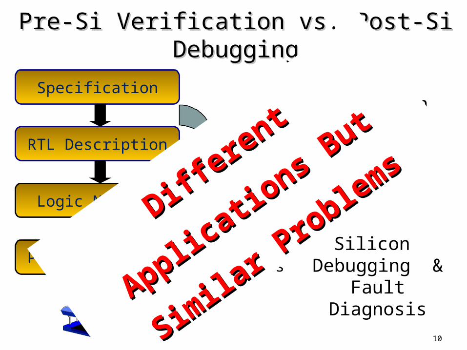
Pre-Si Verification vs. Post-Si Pre-Si Verification vs. Post-Si DebuggingDebugging
Specification
RTL Description
Logic Netlist
Physical Design
Pre-silicon Functional DebuggingInsert
Corrections
Silicon Debugging &
Fault Diagnosis
Insert Faults/ ErrorsDiffe
rent Applic
ations B
ut
Different A
pplicatio
ns But
Simila
r Pro
blems
Simila
r Pro
blems

11
Automated Automated Debugging/DiagnosisDebugging/Diagnosis
Testbenchor
Test Vectors
Design or
Silicon
Verificationor
Testing
PASS
FAIL
Counter examples/Diagnostic Patterns
Automated Debugging/Diagnosis
A failed verification/test step is followed by A failed verification/test step is followed by
debugging/diagnosis:debugging/diagnosis:

12
Leveraging Pre-Si Verification & Leveraging Pre-Si Verification & Manufacturing Test Efforts for Post-Si Manufacturing Test Efforts for Post-Si
ValidationValidation
Specification
RTL Description
Logic Netlist
Physical Design
Pre-silicon verification
Post-silicon validation
12
Manufacturing test
Black BoxBlack Box
Black BoxBlack BoxModels at very Models at very
low level of low level of abstractionabstraction
White BoxWhite BoxLack of error Lack of error propagation propagation
analysis/metricsanalysis/metrics

13
Outline
• Post-Silicon Validation and Debug
• SMT-Based RTL Error Diagnosis [ITC 2008]
• SAT-Based Diagnostic Test Generation [ATS 2007]

14
SAT assignment(s) → Fault location(s)!
SAT-Based DiagnosisSAT-Based Diagnosis
Replicate circuit for each test
Add additional circuitry into circuit model
Add input/output constraints
Erroneous Design Failing Tests

15
SAT-Based Diagnosis - ExampleSAT-Based Diagnosis - Example
• Stuck-at-1 fault on line l1
• Input vector v=(0, 0, 1) detects 1/0 at y
1x
1
x2
x3 yl
1 1 / 0
10
0 0 / 1
Courtesy: A. Veneris

16
SAT-Based Diagnosis – SAT-Based Diagnosis – Example (Cont’d)Example (Cont’d)
1. Insert a MUX at each error candidate location
0
1
x1
x2
x3 yl1
s1
w1
2. Apply input/output vector constraints
0
1
x1
x2
x3 yl1
s1
w1
1
0
0 0
Courtesy: A. Veneris
17
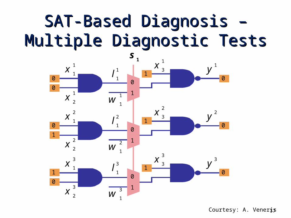
SAT-Based Diagnosis – Multiple SAT-Based Diagnosis – Multiple Diagnostic TestsDiagnostic Tests
0
1
0
1
0
1
0
0
10
0
1
10
1
0
10
x1
1
x2
1
x3
1
y1
l1
1
s1
w1
1
x1
2
x2
2
x3
2
y2
l1
2
w1
2
x1
3
x2
3
x3
3
y3
l1
3
w1
3
Courtesy: A. Veneris

18
RTL Design Error DiagnosisRTL Design Error Diagnosis
• Using Boolean SAT-Solvers for RTL design error diagnosis is not efficient– The translation to Boolean is expensive
– High level information is discarded
18
Propose a SMT-based, automated method for RTL-level
design error diagnosis

19
Satisfiability Modulo Theory Satisfiability Modulo Theory (SMT) Solvers(SMT) Solvers
• Targets combined decision procedures (CDP)
• Integrate Boolean-level approach with higher-level decision procedures, such as ILP
• SHIVA-UIF: an SMT solver developed for RTL circuit
• Boolean Theory
• Bit-vector Theory
• Equality Theory} Makes a good candidate as
the satisfiability engine for hardware designs

20
RTL Design Error Diagnosis Utilizing RTL Design Error Diagnosis Utilizing
SHIVA-UIFSHIVA-UIF• Extend the main idea
of Boolean-SAT-based diagnosis approach to word-level
– MUXs are added to word-level signals
20
Add MUXs to design
SMTUNSAT
Add identified candidate to possible candidate list
SAT
Failing Patterns, Error Candidates
Removeremaining
candidates
Impose test as constraints
Add constraints to avoid same solution
Reduced candidate
list

21
• Simple effect-cause analysis used to limit the potential candidates
• A MUX is inserted at each potential erroneous signal
21
X1
X2L
Y
+=
X3
Initialization StepsInitialization Steps
W
S

22
Could Directly Modifying HDL Code (at Potential Erroneous
Statements) module full_adder_imp (a1, a2, c_in, s, c_out); input a1, a2, c_in; output s, c_out; wire temp;
assign s = a1 ^ a2 ^ c_in; assign temp = (a1 & a2) | (a1 & c_in); assign c_out = temp | (a2 & c_in);
endmodule
module full_adder_muxed (a1, a2, free1, free2, free3, s1, s2, s3, c_in, s, c_out);input a1, a2, c_in;input free1, free2, free3;input s1, s2, s3;output s, c_out;wire temp_mux, s_mux, cout_mux;
assign s_mux = a1 ^ a2 ^ c_in;assign s = s1 ? s_mux : free1;
assign temp_mux = (a1 & a2) | (a1 & c_in);assign temp = s2 ? temp_mux : free2;
assign c_out_mux = temp | (a2 & c_in);assign c_out = s3 ? c_out_mux : free3;
endmodule

23
• Add constraints corresponding to a failing test and its expected response to the MUX-inserted circuit/code
Inserting Constraints w.r.t. Failing Inserting Constraints w.r.t. Failing Test and Expected ResponseTest and Expected Response
23
X1
X2L
Y
+=
W
S
X3
3
5
3
1
( ( S? (W):(3+3) ) = 5 )
SATS = 1W =5

24
Experimental ResultsExperimental Results
• 11 example circuits (IWLS 2005 benchmarks)• An error is randomly injected in each circuit• * after applying simple effect-cause analysis
DesignNo. of word-
level elements
No. of patterns
No. of initial candidates*
No. offinal
candidatesB03 108 4 72 6B04 108 5 72 9B05 9700 28 12949 5C5 115 20 211 13
C10 230 18 561 9C12 420 12 579 100C15 345 13 911 25C16 540 9 595 7C17 720 8 815 28C18 1800 28 2135 10C30 2910 26 3499 87

25
Experimental ResultsExperimental Results
25
• 4 sample circuits, each with 1000 random errors• Average/Max/Minimum number of remaining candidates
26
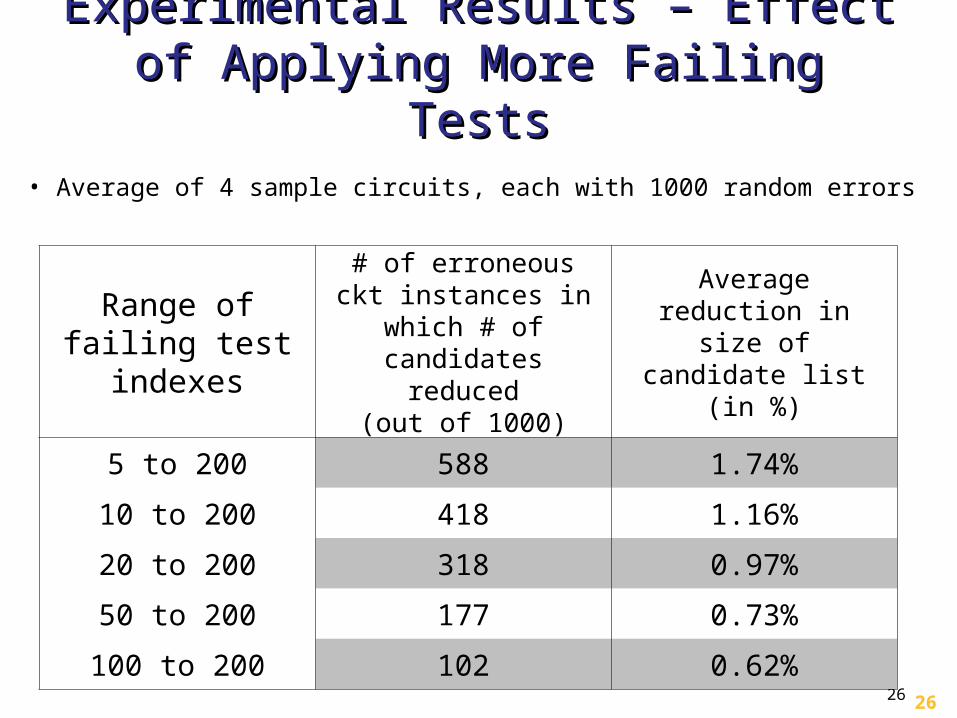
Experimental Results – Effect of Experimental Results – Effect of Applying More Failing TestsApplying More Failing Tests
26
• Average of 4 sample circuits, each with 1000 random errors
Range of failing test
indexes
# of erroneous ckt instances in which
# of candidates reduced
(out of 1000)
Average reduction in size of
candidate list (in %)
5 to 200 588 1.74%
10 to 200 418 1.16%
20 to 200 318 0.97%
50 to 200 177 0.73%
100 to 200 102 0.62%

27
Disadvantage of Model-Free Disadvantage of Model-Free DiagnosisDiagnosis
• Some errors are indistinguishable from each other
• Example: L is the real error location but the solver can find satisfying values for all initial error candidates
Golden Model
X1
X2L
Y
+ =X3 X1
X2L
Y
- =X3
W4
S4
W
5 S
5
W
2S2
W
1
s1W
3
s3
Design

28
Advantages of SMT-Based Advantages of SMT-Based RTL Design Error DiagnosisRTL Design Error Diagnosis
• The learned information can be reused
• The order of candidate identification is easy to difficult, implicitly done by the solver – Solver tends to set MUXs of easy-to-diagnosis candidates
first, and,
– By the time of checking difficult candidates, the accumulated learned clauses help reduce complexity
• Running All-SAT for this model results in:– Eliminating a group of candidates without explicitly
targeting them one at a time

29
Outline
• Post-Silicon Validation and Debug
• SMT-Based RTL Error Diagnosis [ITC 2008]
• SAT-Based Diagnostic Test Generation [ATS 2007]

30
Diagnostic Test Pattern Diagnostic Test Pattern Generation (DTPG)Generation (DTPG)
• Generates tests that distinguish fault types or locations
• One of the most computationally intensive problems
• Most existing methods are based on modified conventional ATPG or Sequential ATPG
• Very complex and tedious implementation
30
Propose an Efficient SAT-based
DTPG approach for combinational
and sequential circuits
31
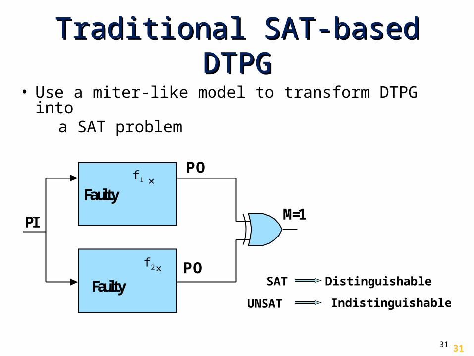
Traditional SAT-based DTPGTraditional SAT-based DTPG• Use a miter-like model to transform DTPG into a SAT problem
SAT Distinguishable
UNSAT Indistinguishable
PI
PO
PO
M=1Faulty
Faulty
×
×f1
f2
31

32
SAT-based DTPGSAT-based DTPG• Limitations:
– Need to build a miter circuit for each fault pair
– Cannot share learned information for different fault pairs
Objectives: Reduce number of miter circuits and the computational cost for each DTPG run by using learned information from previous runs
32

33
DTPG Model for Injecting Multiple DTPG Model for Injecting Multiple Fault PairsFault Pairs
• Inject the same set of N=2n to-be-differentiated faults into each of the two circuits in the miter
• Add a n-to-2n decoder in each circuit to activate exactly one fault at a time
• The extra sets of primary inputs to the decoders, PI1 and PI2, are extra primary inputs
• Solve objective M=1
PI
PO
M=1?
n -2 n D e c o d e rP I1
s e l1
s e l2F a u ltys e lN
PO
n -2 n D e c o d e rP I2
s e l'1
s e l'2F a u ltys e l'N
33
Vi differentiates f1 and f6!!
001
Vi
110

34
DTPG Procedure Using Proposed DTPG Procedure Using Proposed ModelModel• For a SAT solution, values assigned
at PI1 and PI2 represent indices of activated fault pair; values assigned at PI is a diagnostic test
• After diagnostic test of fault pair fi and fj, is found, add a blocking clause to avoid test for the same pair generated again
• After UNSAT, all remaining fault pairs are indistinguishable
Build theDTPG model
M=1?
UNSAT
Diagnostic patternfound
Add SAT constraint
SAT
List of fault candidates
End
Simplify the circuit
34
35
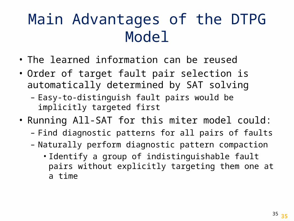
Main Advantages of the DTPG Model
• The learned information can be reused• Order of target fault pair selection is
automatically determined by SAT solving– Easy-to-distinguish fault pairs would be implicitly
targeted first
• Running All-SAT for this miter model could:– Find diagnostic patterns for all pairs of faults– Naturally perform diagnostic pattern compaction
• Identify a group of indistinguishable fault pairs without explicitly targeting them one at a time
35

36
Finding More Compact Diagnostic Finding More Compact Diagnostic TestsTests
36
PI
PO
M=1?
n -2 n D e c o d e rP I1
s e l1
s e l2F a u ltys e lN
PO
n -2 n D e c o d e rP I2
s e l'1
s e l'2F a u ltys e l'N
000
011
Vi
Vi differentiates f0 and f3
0x0
11x
Vj
Vj differentiates {f0, f2} and {f6, f7}

37
DTPG with Compaction DTPG with Compaction HeuristicHeuristic
• Solve objective M = 1 using SAT solver
• Use existing patterns to guide the SAT solving
• Find don’t cares at PI1 and PI2 in the newly
generated pattern - so the corresponding pattern differentiate two groups of faults
37

38
DTPG for Multiple Faults
• Need m n-to-2n decoder in each faulty circuit (m is the cardinality of multiple faults)
• One output from each decoder is connected to an m-input OR gate
• Can inject m or fewer faults
• Combine existing methods before using the proposed DTPG model
n-2de c o de r
n-2de c o de r
....
n n
... ...
.
Se l i
Se l j

39
DTPG ResultsDTPG Results
Circuit#Initial
Fault Pairs#D/#E/#A
#Diagnostic
Patterns
CPU (sec)
S5378 66 63/3/0 13 0.3
S13207 1225 1198/27/0 28 3.9
S15850 231 204/27/0 7 3.3
S35932 120 106/14/0 7 2.0
S38417 351 351/0/0 8 2.9
S38584 1225 1205/20/0 33 7.3
• Initial fault pairs: generated by a critical-path-tracing tool
• All fault pairs injected into one miter circuit• #D—distinguishable, #E—equivalent, #A—aborted
40
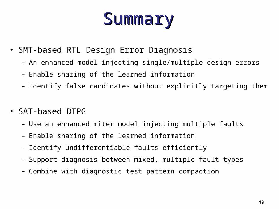
SummarySummary
• SMT-based RTL Design Error Diagnosis– An enhanced model injecting single/multiple design errors
– Enable sharing of the learned information
– Identify false candidates without explicitly targeting them
• SAT-based DTPG– Use an enhanced miter model injecting multiple faults
– Enable sharing of the learned information
– Identify undifferentiable faults efficiently
– Support diagnosis between mixed, multiple fault types
– Combine with diagnostic test pattern compaction
Related Documents


![Debugging Design [EN]](https://static.cupdf.com/doc/110x72/5457c036b1af9fc15d8b4854/debugging-design-en.jpg)