1 CHAPTER 8 MOBILITY

1 CHAPTER 8 MOBILITY. 2 8.1 INTRODUCTION 3 High mobility material has higher frequency response and higher current. Electron-electron or hole-hole scattering.
Dec 21, 2015
Welcome message from author
This document is posted to help you gain knowledge. Please leave a comment to let me know what you think about it! Share it to your friends and learn new things together.
Transcript
1
CHAPTER 8
MOBILITY
2
8.1 INTRODUCTION

3
8.1 INTRODUCTION
• High mobility material has higher frequency response and higher current.
• Electron-electron or hole-hole scattering has no first-order effect on the mobility. Electron-hole scattering reduces the mobility.
• Minority carriers has ionized impurity scattering and electron-hole scattering, majority carriers has ionized impurity scattering.
4
8.2 CONDUCTIVITY
MOBILITY

5
CONDUCTIVITY MOBILITY
Measure the majority carrier concentration and the conductivity/resistivity is sufficient to calculate the conductivity mobility.
For p-type material.

6
8.3 HALL EFFECT
AND MOBILITY

7
Basic Equations for Uniform Layers or Wafers
Schematic illustrating the Hall effect in a p-type sample.

8
Hall angle is defined as the angle between Ex and Ey.

9
For p-type sample.
For n-type sample.
When both carriers present.
10
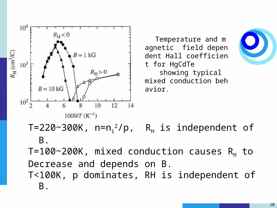
Temperature and magnetic field dependent Hall coefficient for HgCdTe
showing typical mixed conduction behavior.
T=220~300K, n=ni2/p, RH is independent of B.
T=100~200K, mixed conduction causes RH to Decrease and depends on B.T<100K, p dominates, RH is independent of B.
11
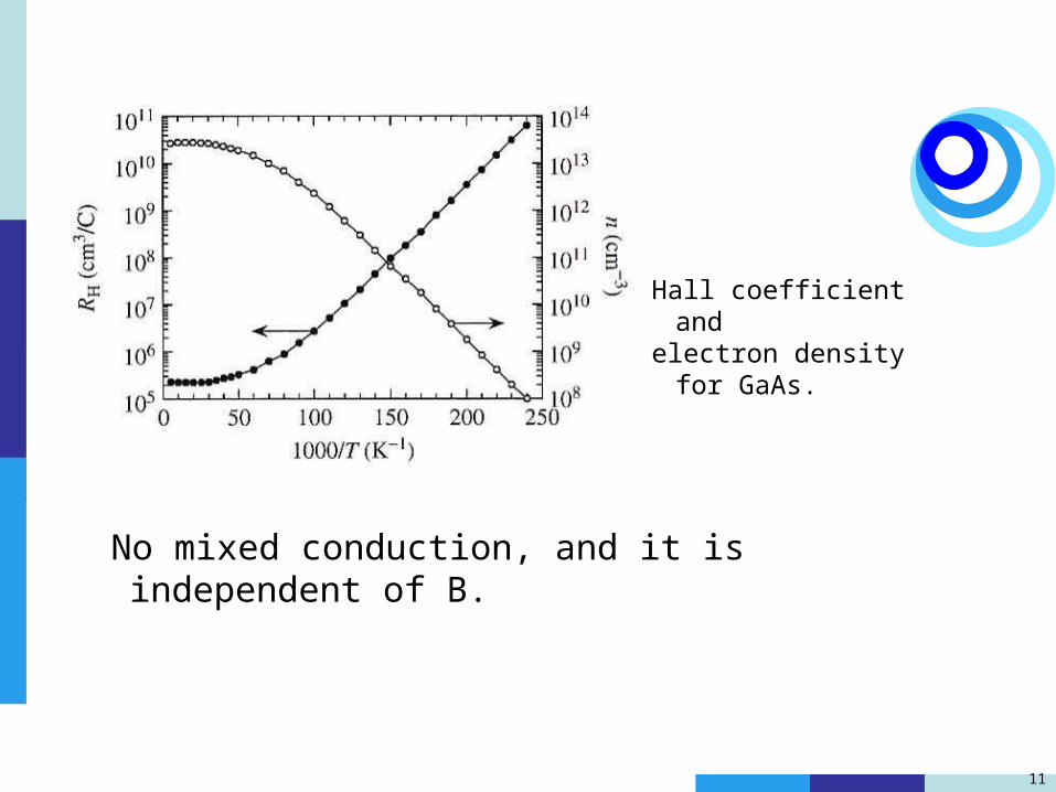
Hall coefficient and electron density for GaAs.
No mixed conduction, and it is independent of B.

12
The above results are based on the assumption of energy-independent scattering mechanisms.If it is relaxed, the Hall scattering factor r must be Included:

13
(a) Bridge-type Hall sample, (b) lamella-type van der Pauw Hall sample.
R12,34=V34/I12, V34=V4-V3
F is a function of Rr=R12,34/R23,41
For symmetric samples F=1.
ΔR24,13 is the difference with and without the magnetic field.
14
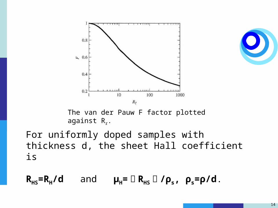
The van der Pauw F factor plotted against Rr.
For uniformly doped samples with thickness d, the sheet Hall coefficient is
RHS=RH/d and μH=︳ RHS︳ /ρs, ρs=ρ/d.

15
Nonuniform Layers
Hall measurements give average values,assuming r=1:
16
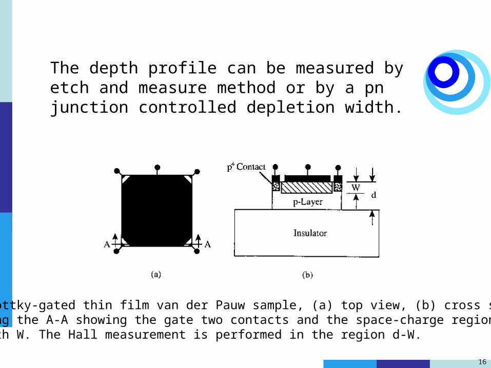
The depth profile can be measured by etch and measure method or by a pn junction controlled depletion width.
Schottky-gated thin film van der Pauw sample, (a) top view, (b) cross section along the A-A showing the gate two contacts and the space-charge region of width W. The Hall measurement is performed in the region d-W.
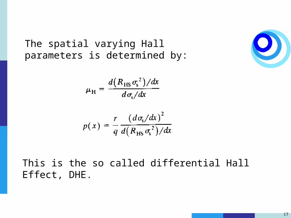
17
The spatial varying Hall parameters is determined by:
This is the so called differential Hall Effect, DHE.
18
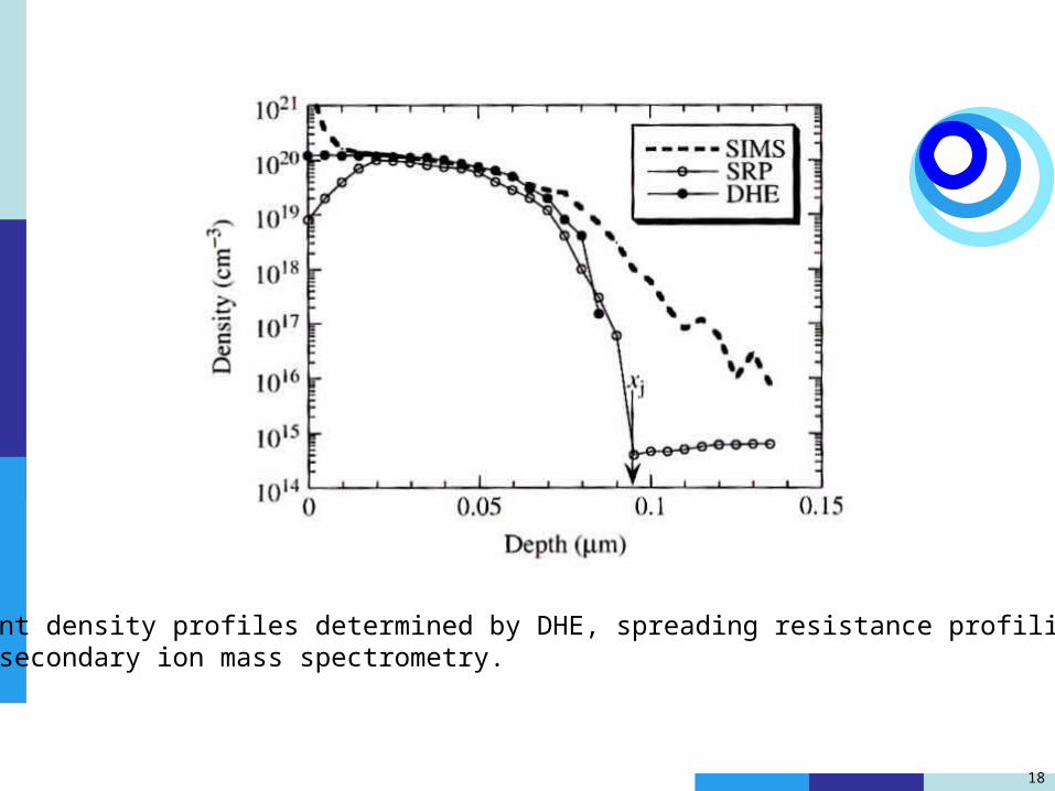
Dopant density profiles determined by DHE, spreading resistance profiling, and secondary ion mass spectrometry.
19
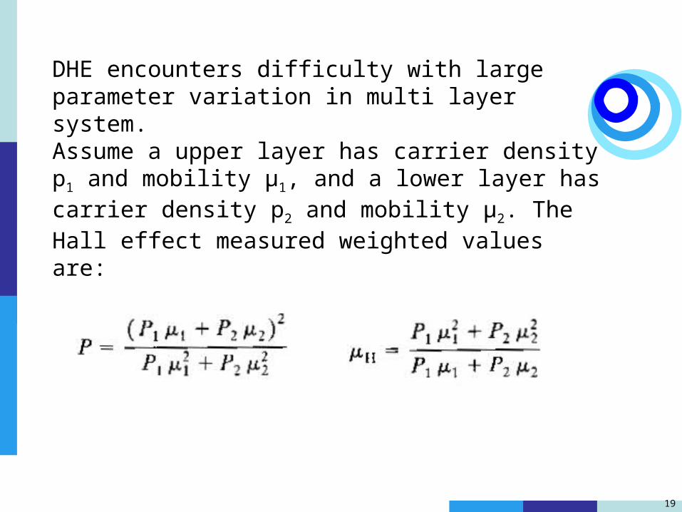
DHE encounters difficulty with large parameter variation in multi layer system.Assume a upper layer has carrier density p1 and mobility μ1, and a lower layer has carrier density p2 and mobility μ2. The Hall effect measured weighted values are:
20
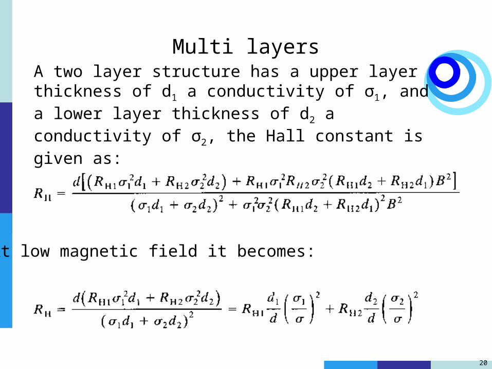
Multi layers
A two layer structure has a upper layer thickness of d1 a conductivity of σ1, and a lower layer thickness of d2 a conductivity of σ2, the Hall constant is given as:
At low magnetic field it becomes:
21
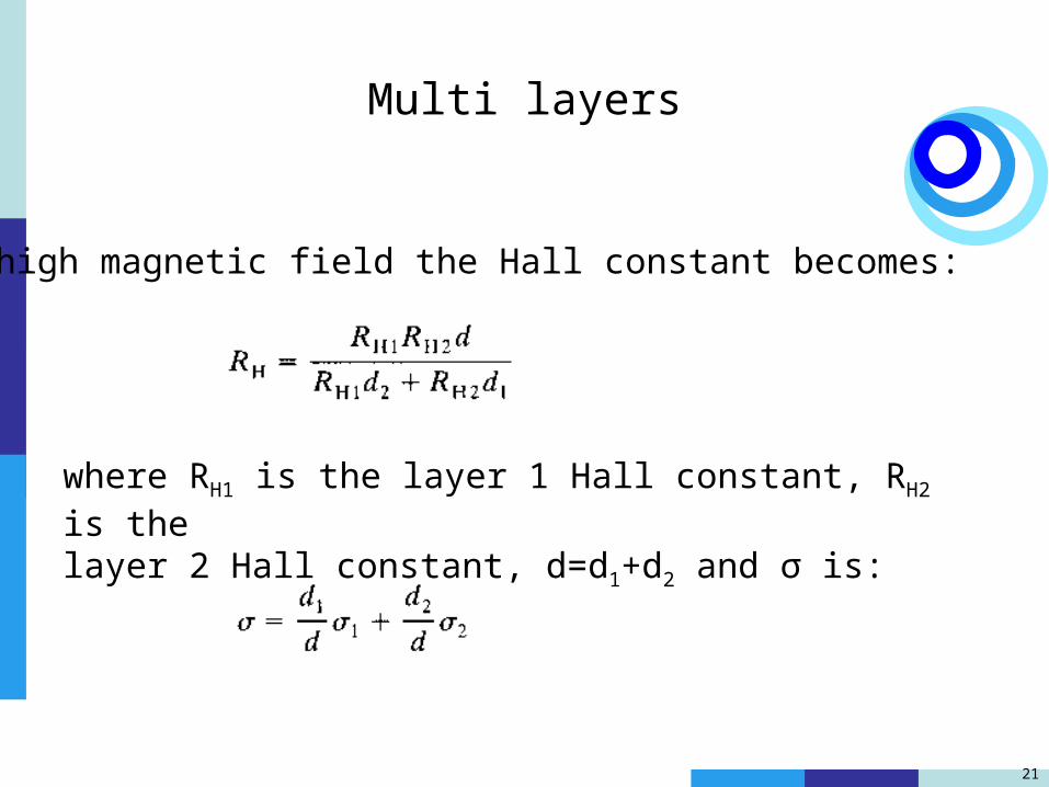
Multi layers
At high magnetic field the Hall constant becomes:
where RH1 is the layer 1 Hall constant, RH2 is thelayer 2 Hall constant, d=d1+d2 and σ is:
22
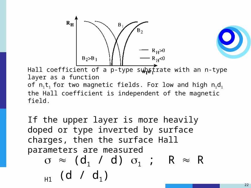
Hall coefficient of a p-type substrate with an n-type layer as a function of n1t1 for two magnetic fields. For low and high n1d1 the Hall coefficient is independent of the magnetic field.
If the upper layer is more heavily doped or type inverted by surface charges, then the surface Hall parameters are measured
(d1 / d) 1 ; R RH1 (d / d1)

23
Sample Shapes and Measurement Circuits
(a) Bridge-type Hall configuration, (b)-(d) lamella-type Hall configuration.
24
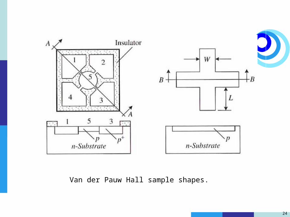
Van der Pauw Hall sample shapes.

25
Effect of non-ideal contact length or contact placement on the resistivity and mobility for van der Pauw samples.
26
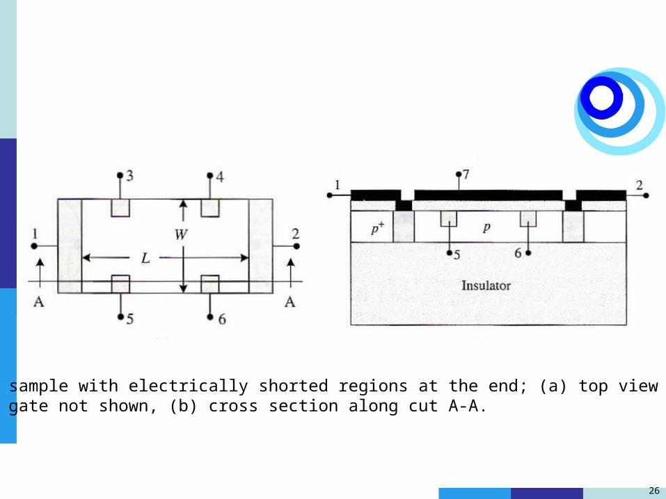
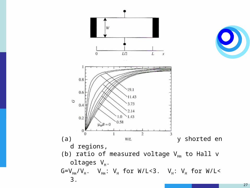
Hall sample with electrically shorted regions at the end; (a) top view with the gate not shown, (b) cross section along cut A-A.
27
(a) Hall sample with electrically shorted end regions, (b) ratio of measured voltage VHm to Hall voltages VH. G=VHm/VH. VHm: VH for W/L<3. VH: VH for W/L<3.
28
8.4 MAGNETORESISTANCE
MOBILITY

29
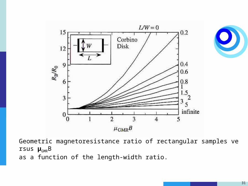
MAGNETORESISTANCE MOBILITY
(a) Hall sample, (b) short, wide sample, Hall voltage is nearly shorted;(c) Corbino disk, Hall voltage is shorted. They can be used to measure t
he magnetoresistance effect.

30
Physical magnetoresistance effect (PMR):The sample resistance increases when it is placed in a magnetic field. Because the conduction is anisotropic, involves more than one type of carrier, and carrier scattering is energy dependent. Geometrical magnetoresistance effect (GMR):The charge carrier path deviates from a straight line.
ξ=( 〈 τ3〉〈 τ〉 / 〈 τ2〉 2)2 is the magnetoresistance scattering factor.
GMR = H
31
Geometric magnetoresistance ratio of rectangular samples versus μGMRB as a function of the length-width ratio.

32
For Corbino disc.
For rectangular samples with low L/W ratio and μGMRB<1
For determining the error in μGMR to be <10%, then L/W must be <0.4.

33
8.5 TIME-OF-FIGHT
DRIFT MOBILITY

34
(a) Drift mobility measurement arrange-ment and normalized output voltage pulse (μp=180cm2/V. s,τn=0.67 μs, T=423K, =60V/cm)

35
(b) output voltage pulses (μn=1000 cm2/V. s,τn=1μs, T=300K, =100V/cm, N=1011 cm-2), (c) output voltage pulses (μn=1000cm2/ V. s, d=0.075cm, T=300K, =100V/cm, N=1011cm-2). td=0.75us.
36
TIME-OF-FLIGHT DRIFT MOBILITY
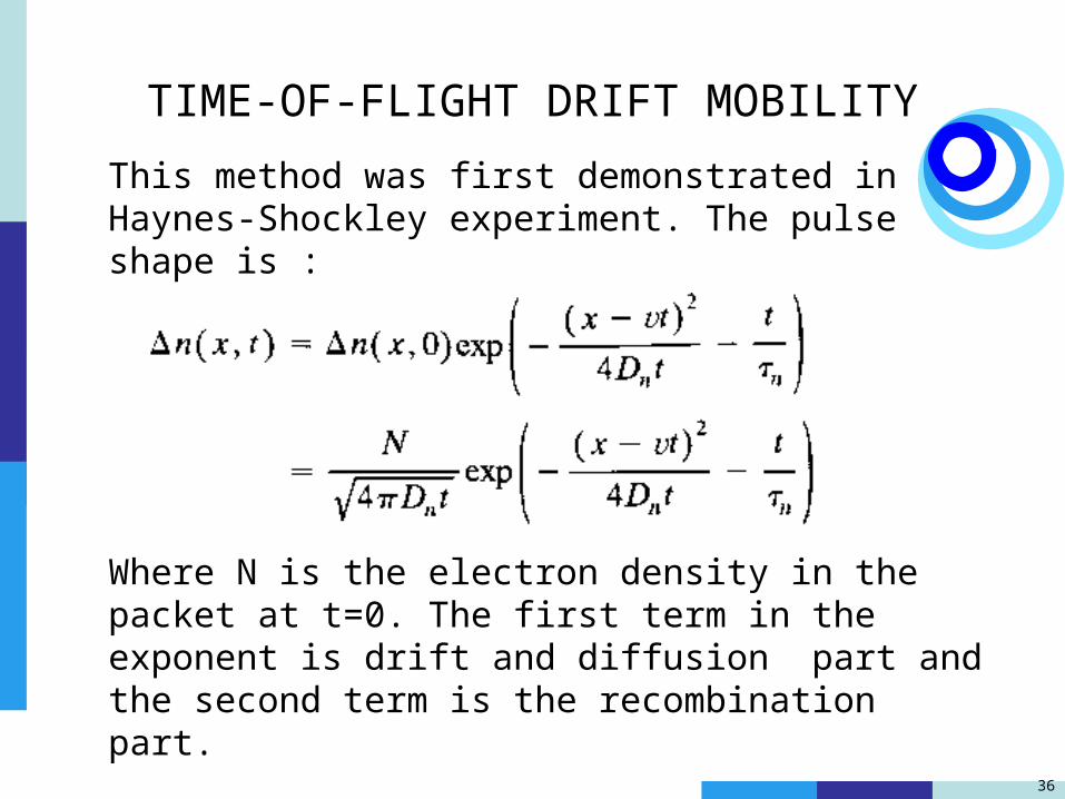
This method was first demonstrated in Haynes-Shockley experiment. The pulse shape is :
Where N is the electron density in the packet at t=0. The first term in the exponent is drift and diffusion part and the second term is the recombination part.
37
TIME-OF-FLIGHT DRIFT MOBILITY
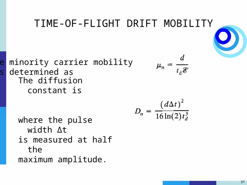
The minority carrier mobility is determined as
The diffusion constant is
where the pulse width Δtis measured at half themaximum amplitude.
38
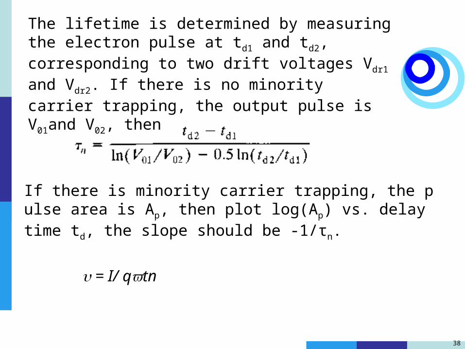
The lifetime is determined by measuring the electron pulse at td1 and td2, corresponding to two drift voltages Vdr1 and Vdr2. If there is no minority carrier trapping, the output pulse is V01and V02, then
If there is minority carrier trapping, the pulse area is Ap, then plot log(Ap) vs. delay time td, the slope should be -1/τn.
= I/ qtn

39
(a) Time-of-flight measurement schematic, (b) output voltage for tt«RC, The dashed lines indicate the effect of carrier trapping. (c) output voltage for tt»RC, (d) implementation with a p+πn+ diode, both carriers can be measured.

40
From the above system, QN=qN=QA+QC
At t=0 QA=0, at t=tt QA=QN, where tt is the transit time
When QA changes from 0 to QN the external current is:
41
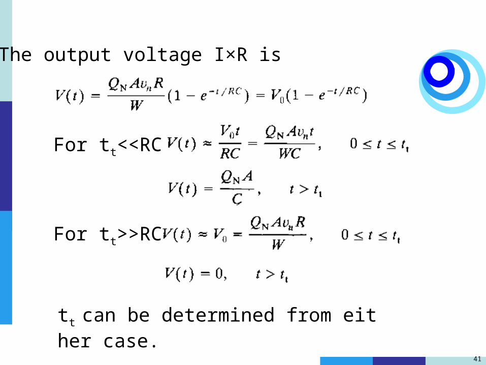
The output voltage I×R is
For tt<<RC
For tt>>RC
tt can be determined from either case.

42
Two drift mobility measurement implemen-tations as discussed in the text.
43
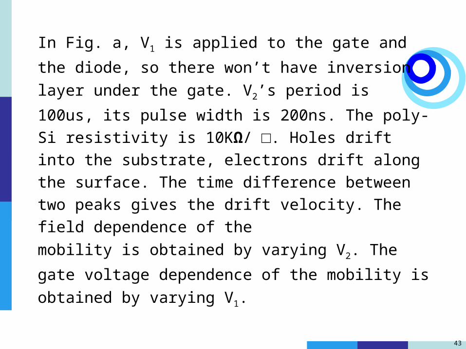
In Fig. a, V1 is applied to the gate and the diode, so there
won’t have inversion layer under the gate. V2’s period is
100us, its pulse width is 200ns. The poly-Si resistivity is
10KΩ/ □. Holes drift into the substrate, electrons drift
along the surface. The time difference between two
peaks gives the drift velocity. The field dependence of the
mobility is obtained by varying V2. The gate voltage
dependence of the mobility is obtained by varying V1.
44
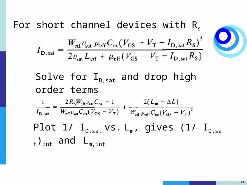
For short channel devices with Rs
Solve for ID,sat and drop high order terms
Plot 1/ ID,sat vs. Lm, gives (1/ ID,sat)int and Lm,int

45
Substituting (1/ ID,sat)int into Lm,int gives
The above equation contains no μeff.

46
Plotting Lm,int vs. Lm,int /(1/ ID,sat)int has the slope A. Plotting A vs. 1/ (VGS-VT) gives the line with slope S.
The saturation velocity is
sat=1/ (WeffCox(S-2Rs))

47
8.6 MOSFET MOBILITY

48
MOSFET MOBILITY
There are many kinds of mobility due to : lattice (phonon) scattering, ionized impurity scattering,neutral impurity scattering, piezoelectric scattering, or surface scattering. According to Mathiessen’s rule
49
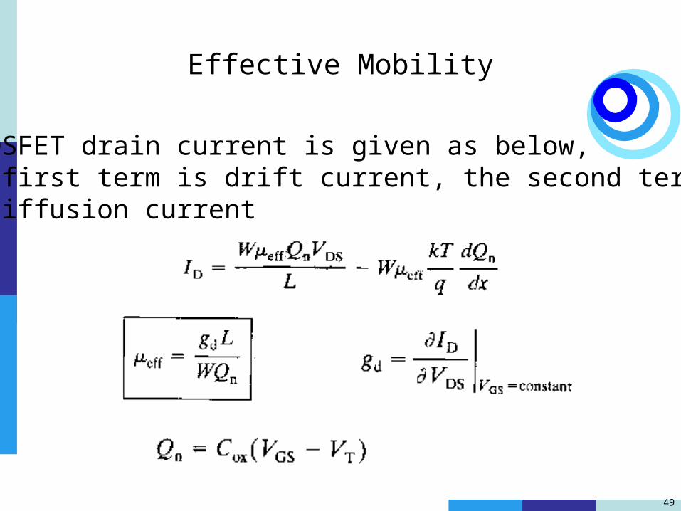
Effective Mobility
A MOSFET drain current is given as below,the first term is drift current, the second term is diffusion current
50
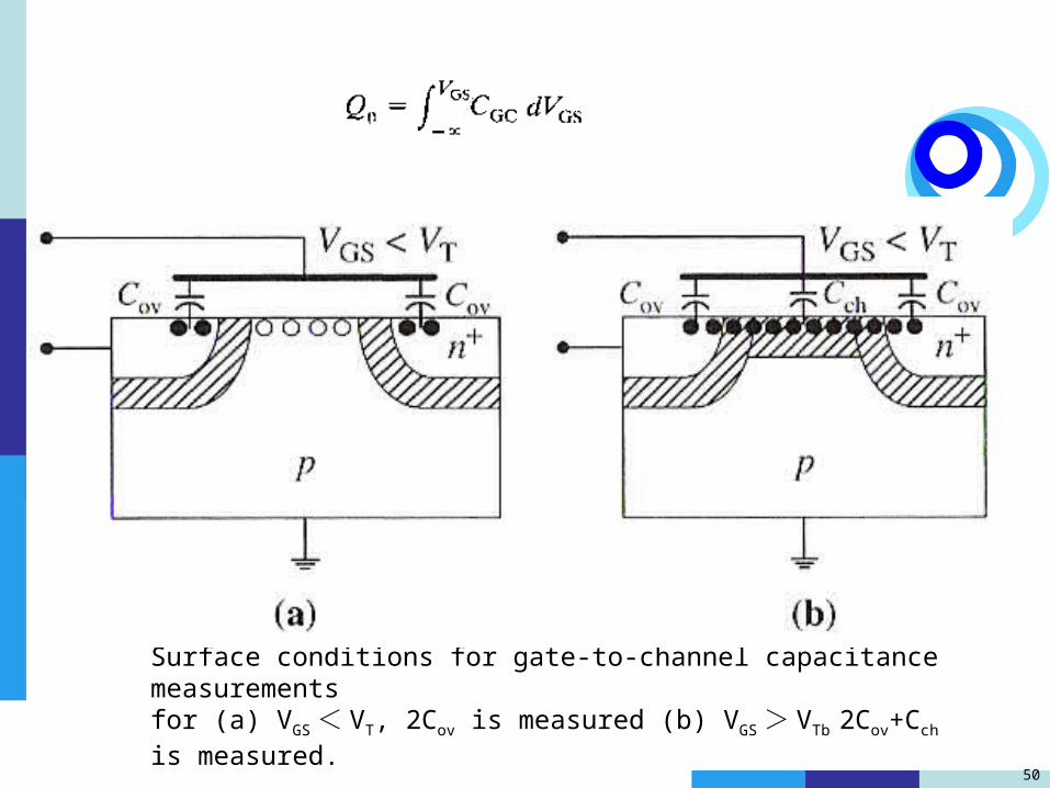
Surface conditions for gate-to-channel capacitance measurements for (a) VGS< VT, 2Cov is measured (b) VGS> VTb 2Cov+Cch is measured.
51
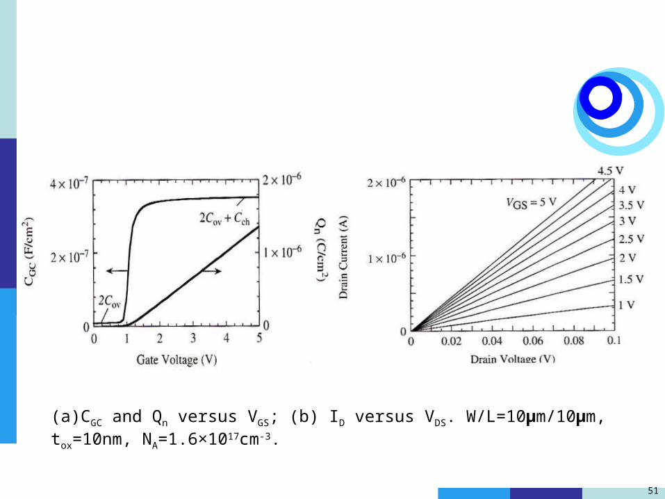
(a) CGC and Qn versus VGS; (b) ID versus VDS. W/L=10μm/10μm, tox=10nm, NA=1.6×1017cm-3.

52
μeff versus VGS for the data of Fig. VT=0.5V.
Once Qn and gd are obtained,μeff can be calculated.

53
Split C-V measurement arrangement.
Qn can be obtained from I1.
Qb and substrate doping profile can be found.
54
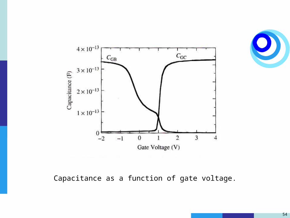
Capacitance as a function of gate voltage.

55
The electric field isvertical field.
η=1/2 for electron mobility,1/3 for hole mobility.

56
(a) Electron and (b) hole effective mobility as a function of effective field. Data taken from the references in the inserts.
57
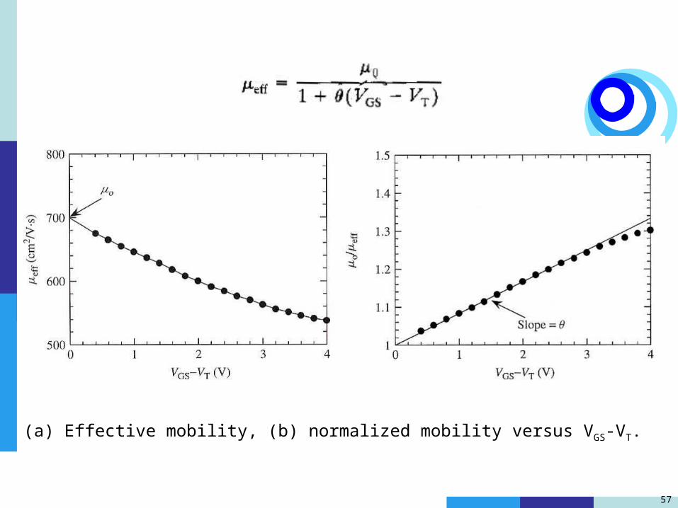
(a) Effective mobility, (b) normalized mobility versus VGS-VT.

58
Effect of Gate Depletion and Channel Location
Simulated Gate-to-channel Capacitance Versus Gate Voltage as a function of poly-Si gate doping density. Oxide leakage current not considered. tox=2nm, NA=1.69×1017cm-3 μeff =300
cm2/V-s

59
MOSFET Cross Section Showing Drain and Gate Current, gate current adds to source current and subtracts drain current
CoxCGC=
1+Cox/CG +Cox/Cch
ID,eff = ID + IG/2
ID,eff = ID = ID(VDS2) - ID (VDS1)

60
Drain and Gate Currents Versus Gate Voltage for n-channel MOSFET
Gate insulator: HfO2~2nm thick. With permission of W. Zhu and T.P. Ma, Yale University

61
Effect of Inversion Charge Frequency Response
Showing source and drain resistance (RS and RD),inversion layer resistance Rch, overlap, oxide, channel and bulk capacitance (Cov,Cox,Cch, and Cb)
Cox Cch tanh()CGC= Re ( )
Cox+Cch+Cb
= (j 0.25C’RchL2)½
62
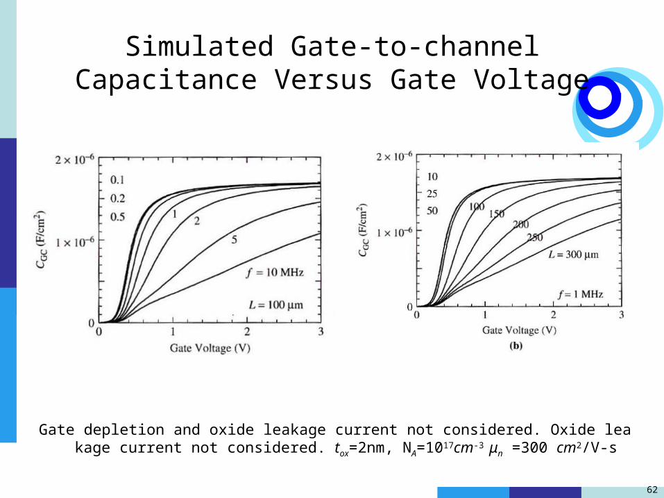
Simulated Gate-to-channel Capacitance Versus Gate Voltage
(a) Frequency (b) Channel Length
Gate depletion and oxide leakage current not considered. Oxide leakage current not considered. tox=2nm, NA=1017cm-3 μn =300 cm2/V-s
63
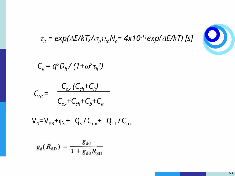
VG=VFB+s+ Qs/Cox± Qit/Cox
Cox (Cch+Cit)CGC=
Cox+Cch+Cb+Cit
Cit = q2Dit / (1+2it2)
it = exp(E/kT)/nthNc= 4x10-11exp(E/kT) [s]
64
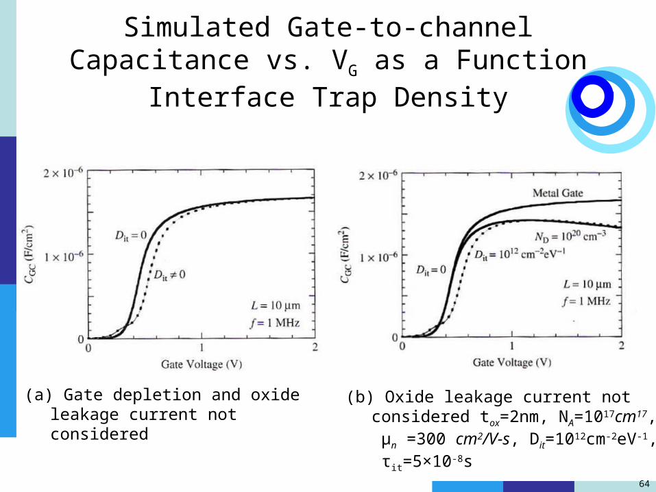
Simulated Gate-to-channel Capacitance vs. VG as a Function Interface Trap Density
(a) Gate depletion and oxide leakage current not considered
(b) Oxide leakage current not considered tox=2nm, NA=1017cm17, μn =300 cm2/V-s, Dit=1012cm-2eV-1, τit=5×10⁻⁸s
65
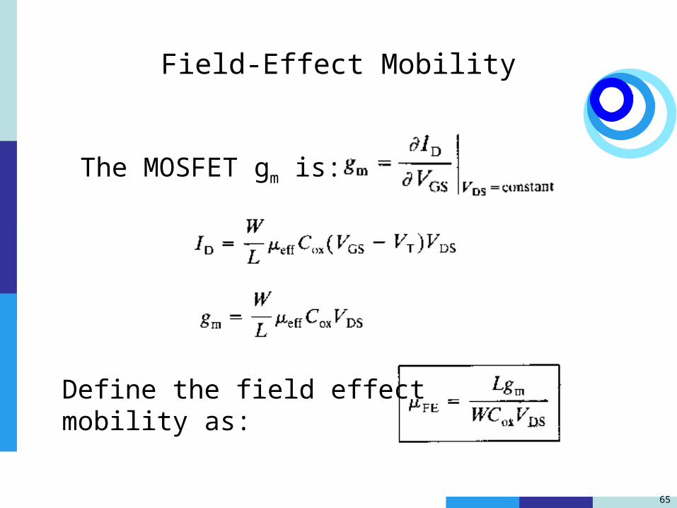
Field-Effect Mobility
The MOSFET gm is:
Define the field effectmobility as:

66
Effective and field-effect mobilities.

67
If we take the μeff dependence on VG into consideration, then

68
When MOSFET operates in saturation region the drain current is:
B represents the body effect. If m is the slope of (ID,sat)1/2 vs. (VGS-VT), then
Related Documents