1 Bipolar Junction Transistors (BJTs)

1 Bipolar Junction Transistors (BJTs). Figure 5.1 A simplified structure of the npn transistor.
Dec 21, 2015
Welcome message from author
This document is posted to help you gain knowledge. Please leave a comment to let me know what you think about it! Share it to your friends and learn new things together.
Transcript

1
Bipolar JunctionTransistors (BJTs)

Figure 5.1 A simplified structure of the npn transistor.

Figure 5.2 A simplified structure of the pnp transistor.

Figure 5.3 Current flow in an npn transistor biased to operate in the active mode. (Reverse current components due to drift of thermally generated minority carriers are not shown.)

Figure 5.4 Profiles of minority-carrier concentrations in the base and in the emitter of an npn transistor operating in the active mode: vBE 0 and vCB 0.

Figure 5.5 Large-signal equivalent-circuit models of the npn BJT operating in the forward active mode.
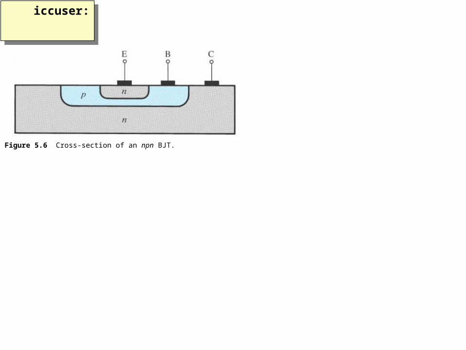
Figure 5.6 Cross-section of an npn BJT.
iccuser:iccuser:

Figure 5.7 Model for the npn transistor when operated in the reverse active mode (i.e., with the CBJ forward biased and the EBJ reverse biased).
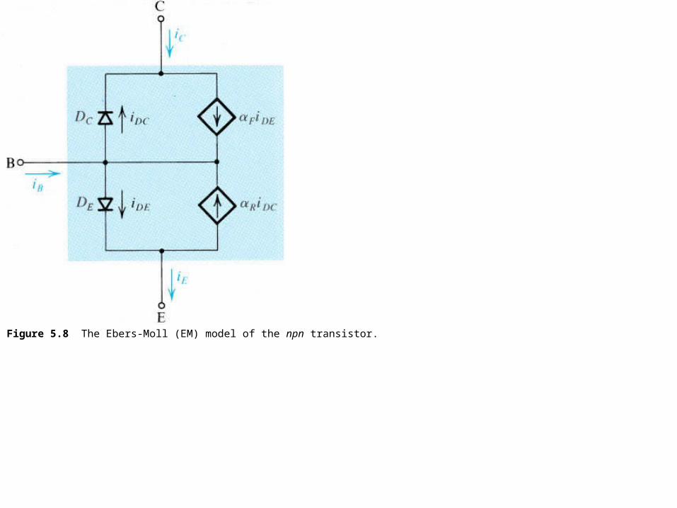
Figure 5.8 The Ebers-Moll (EM) model of the npn transistor.

Figure 5.9 The iC –vCB characteristic of an npn transistor fed with a constant emitter current IE. The transistor enters the saturation mode of operation for vCB –0.4 V, and the collector current diminishes.

Figure 5.10 Concentration profile of the minority carriers (electrons) in the base of an npn transistor operating in the saturation mode.

Figure 5.11 Current flow in a pnp transistor biased to operate in the active mode.
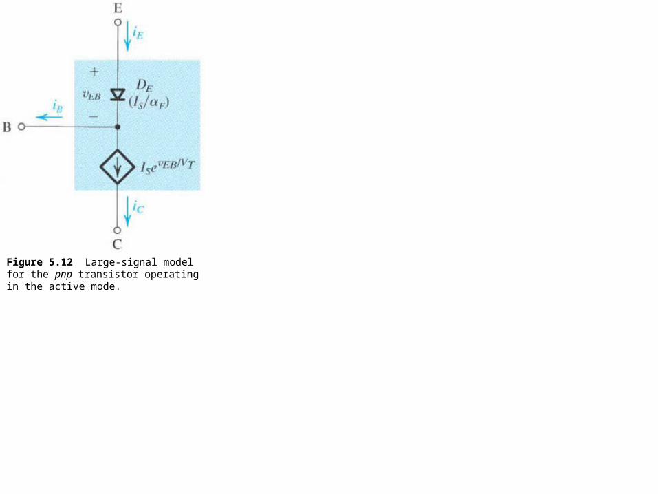
Figure 5.12 Large-signal model for the pnp transistor operating in the active mode.

Figure 5.13 Circuit symbols for BJTs.

Figure 5.14 Voltage polarities and current flow in transistors biased in the active mode.

Figure 5.15 Circuit for Example 5.1.

Figure E5.10

Figure E5.11

Figure 5.16 The iC –vBE characteristic for an npn transistor.

Figure 5.17 Effect of temperature on the iC–vBE characteristic. At a constant emitter current (broken line), vBE changes by –2 mV/C.

Figure 5.18 The iC–vCB characteristics of an npn transistor.

Figure 5.19 (a) Conceptual circuit for measuring the iC –vCE characteristics of the BJT. (b) The iC –vCE characteristics of a practical BJT.

Figure 5.20 Large-signal equivalent-circuit models of an npn BJT operating in the active mode in the common-emitter configuration.

Figure 5.21 Common-emitter characteristics. Note that the horizontal scale is expanded around the origin to show the saturation region in some detail.

Figure 5.22 Typical dependence of on IC and on temperature in a modern integrated-circuit npn silicon transistor intended for operation around 1 mA.
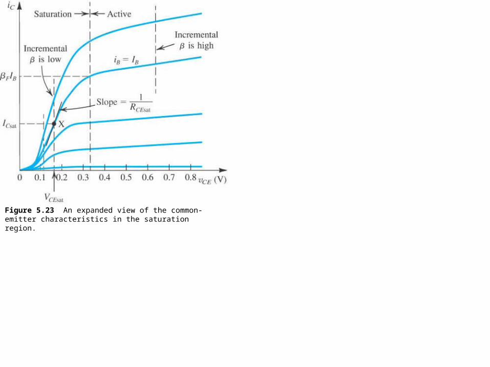
Figure 5.23 An expanded view of the common-emitter characteristics in the saturation region.

Figure 5.24 (a) An npn transistor operated in saturation mode with a constant base current IB. (b) The iC–vCE characteristic curve corresponding to iB = IB. The curve can be approximated by a straight line of slope 1/RCEsat. (c) Equivalent-circuit representation of the saturated transistor. (d) A simplified equivalent-circuit model of the saturated transistor.

Figure 5.25 Plot of the normalized iC versus vCE for an npn transistor with F = 100 and R = 0.1. This is a plot of Eq. (5.47), which is derived using the Ebers-Moll model.

Figure E5.18

Table 5.3

Table 5.3 (Continued)

Figure 5.26 (a) Basic common-emitter amplifier circuit. (b) Transfer characteristic of the circuit in (a). The amplifier is biased at a point Q, and a small voltage signal vi is superimposed on the dc bias voltage VBE. The resulting output signal vo appears superimposed on the dc collector voltage VCE. The amplitude of vo is larger than that of vi by the voltage gain Av.

Figure 5.27 Circuit whose operation is to be analyzed graphically.

Figure 5.28 Graphical construction for the determination of the dc base current in the circuit of Fig. 5.27.

Figure 5.29 Graphical construction for determining the dc collector current IC and the collector-to-emitter voltage VCE in the circuit of Fig. 5.27.

Figure 5.30 Graphical determination of the signal components vbe, ib, ic, and vce when a signal component vi is superimposed on the dc voltage VBB (see Fig. 5.27).

Figure 5.31 Effect of bias-point location on allowable signal swing: Load-line A results in bias point QA with a corresponding VCE which is too close to VCC and thus limits the positive swing of vCE. At the other extreme, load-line B results in an operating point too close to the saturation region, thus limiting the negative swing of vCE.

Figure 5.32 A simple circuit used to illustrate the different modes of operation of the BJT.

Figure 5.33 Circuit for Example 5.3.

Figure 5.34 Analysis of the circuit for Example 5.4: (a) circuit; (b) circuit redrawn to remind the reader of the convention used in this book to show connections to the power supply; (c) analysis with the steps numbered.

Figure 5.35 Analysis of the circuit for Example 5.5. Note that the circled numbers indicate the order of the analysis steps.

Figure 5.36 Example 5.6: (a) circuit; (b) analysis with the order of the analysis steps indicated by circled numbers.

Figure 5.37 Example 5.7: (a) circuit; (b) analysis with the steps indicated by circled numbers.

Figure 5.38 Example 5.8: (a) circuit; (b) analysis with the steps indicated by the circled numbers.

Figure 5.39 Example 5.9: (a) circuit; (b) analysis with steps numbered.

Figure 5.40 Circuits for Example 5.10.

Figure 5.41 Circuits for Example 5.11.

Figure E5.30

Figure 5.42 Example 5.12: (a) circuit; (b) analysis with the steps numbered.

Figure 5.43 Two obvious schemes for biasing the BJT: (a) by fixing VBE; (b) by fixing IB. Both result in wide variations in IC and hence in VCE and therefore are considered to be “bad.” Neither scheme is recommended.

Figure 5.44 Classical biasing for BJTs using a single power supply: (a) circuit; (b) circuit with the voltage divider supplying the base replaced with its Thévenin equivalent.
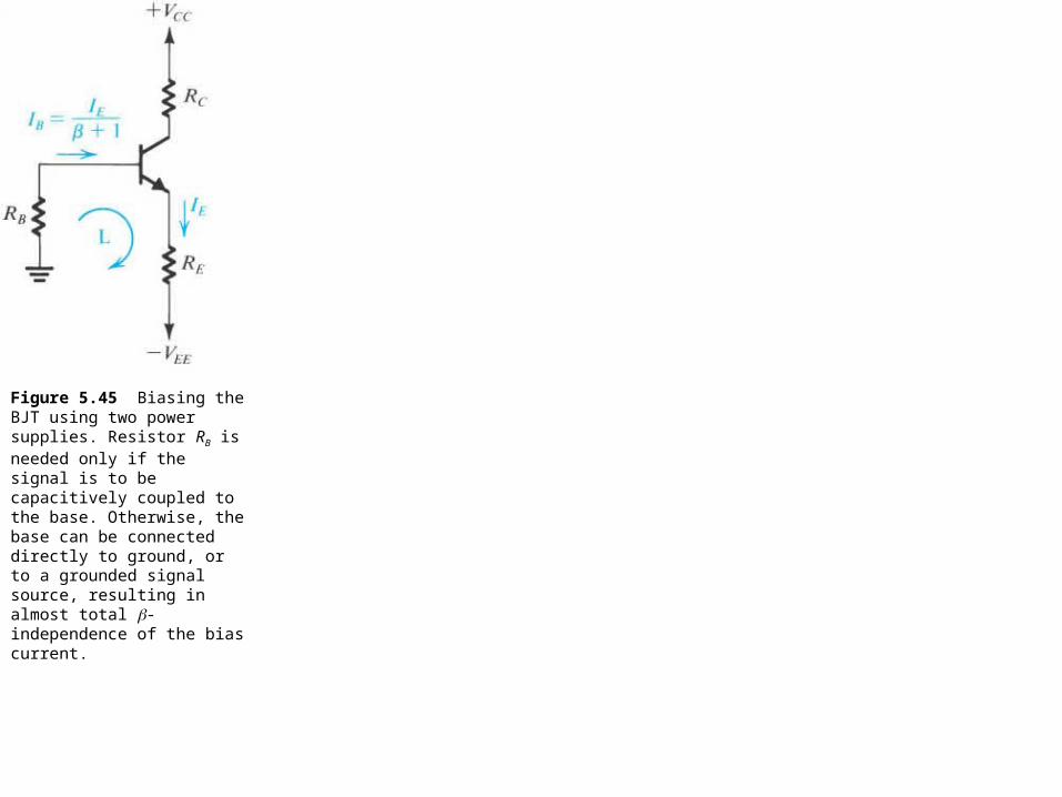
Figure 5.45 Biasing the BJT using two power supplies. Resistor RB is needed only if the signal is to be capacitively coupled to the base. Otherwise, the base can be connected directly to ground, or to a grounded signal source, resulting in almost total -independence of the bias current.
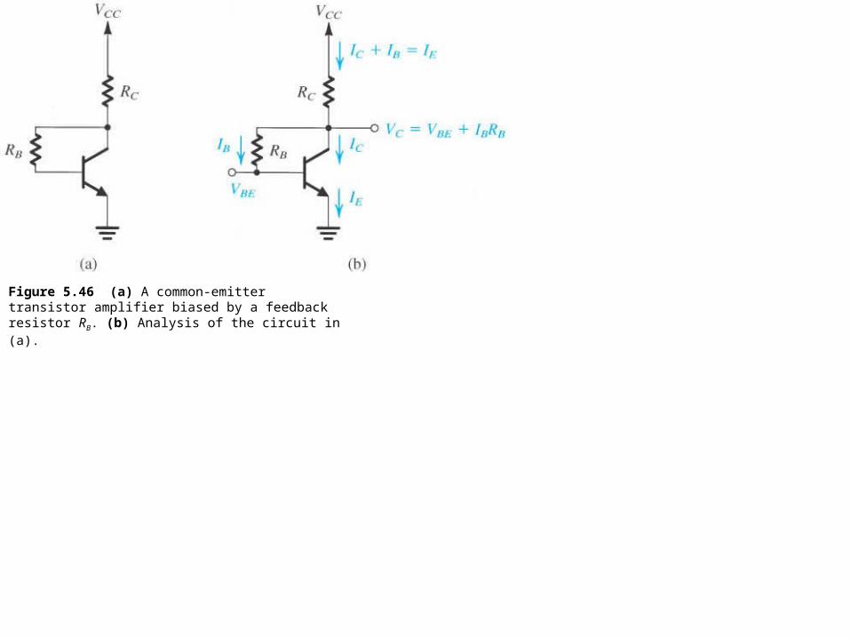
Figure 5.46 (a) A common-emitter transistor amplifier biased by a feedback resistor RB. (b) Analysis of the circuit in (a).

Figure 5.47 (a) A BJT biased using a constant-current source I. (b) Circuit for implementing the current source I.

Figure 5.48 (a) Conceptual circuit to illustrate the operation of the transistor as an amplifier. (b) The circuit of (a) with the signal source vbe eliminated for dc (bias) analysis.

Figure 5.49 Linear operation of the transistor under the small-signal condition: A small signal vbe with a triangular waveform is superimposed on the dc voltage VBE. It gives rise to a collector signal current ic, also of triangular waveform, superimposed on the dc current IC. Here, ic = gmvbe, where gm is the slope of the iC–vBE curve at the bias point Q.

Figure 5.50 The amplifier circuit of Fig. 5.48(a) with the dc sources (VBE and VCC) eliminated (short circuited). Thus only the signal components are present. Note that this is a representation of the signal operation of the BJT and not an actual amplifier circuit.

Figure 5.51 Two slightly different versions of the simplified hybrid- model for the small-signal operation of the BJT. The equivalent circuit in (a) represents the BJT as a voltage-controlled current source (a transconductance amplifier), and that in (b) represents the BJT as a current-controlled current source (a current amplifier).

Figure 5.52 Two slightly different versions of what is known as the T model of the BJT. The circuit in (a) is a voltage-controlled current source representation and that in (b) is a current-controlled current source representation. These models explicitly show the emitter resistance re rather than the base resistance r featured in the hybrid- model.

Figure 5.53 Example 5.14: (a) circuit; (b) dc analysis; (c) small-signal model.

Figure 5.54 Signal waveforms in the circuit of Fig. 5.53.
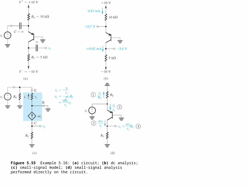
Figure 5.55 Example 5.16: (a) circuit; (b) dc analysis; (c) small-signal model; (d) small-signal analysis performed directly on the circuit.

Figure 5.56 Distortion in output signal due to transistor cutoff. Note that it is assumed that no distortion due to the transistor nonlinear characteristics is occurring.

Figure 5.57 Input and output waveforms for the circuit of Fig. 5.55. Observe that this amplifier is noninverting, a property of the common-base configuration.
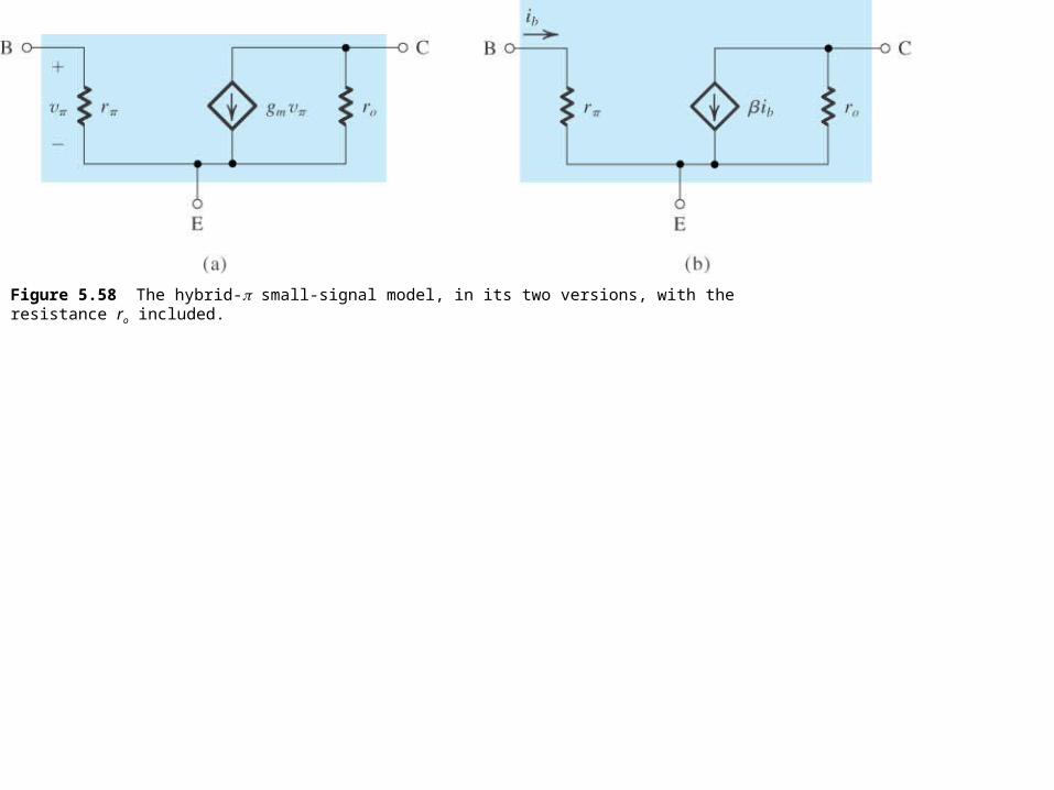
Figure 5.58 The hybrid- small-signal model, in its two versions, with the resistance ro included.

Figure E5.40

Table 5.4

Figure 5.59 Basic structure of the circuit used to realize single-stage, discrete-circuit BJT amplifier configurations.

Figure E5.41

Table 5.5

Figure 5.60 (a) A common-emitter amplifier using the structure of Fig. 5.59. (b) Equivalent circuit obtained by replacing the transistor with its hybrid- model.
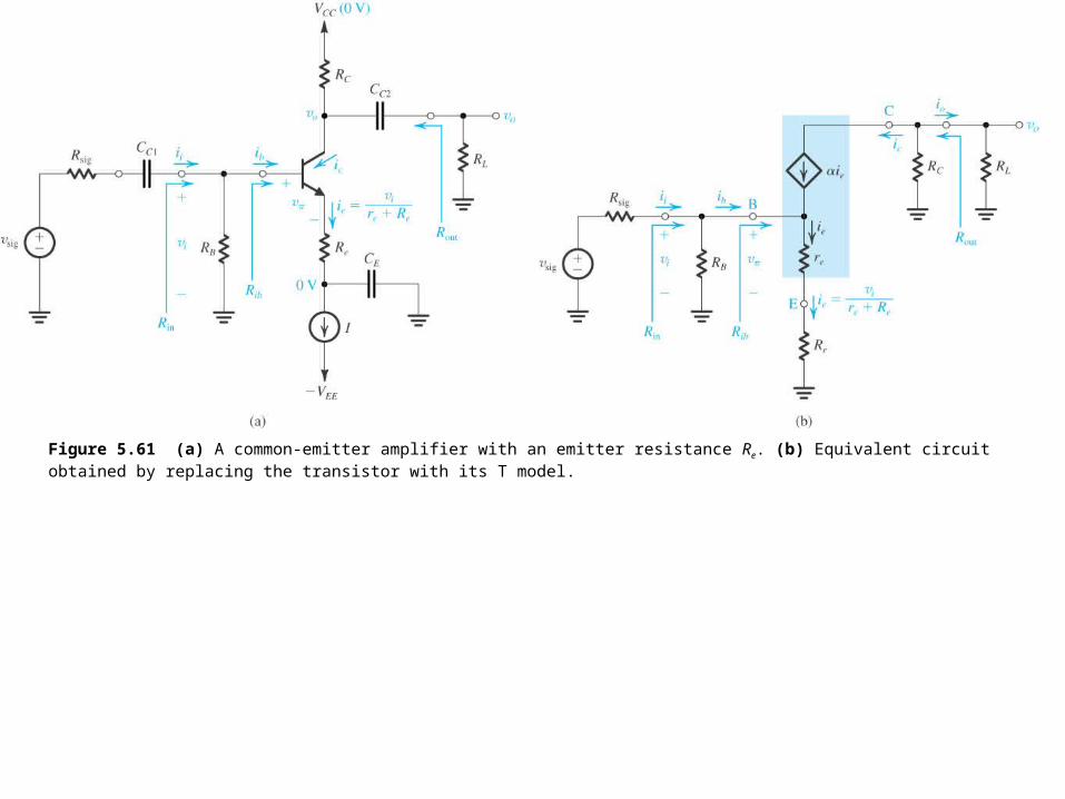
Figure 5.61 (a) A common-emitter amplifier with an emitter resistance Re. (b) Equivalent circuit obtained by replacing the transistor with its T model.

Figure 5.62 (a) A common-base amplifier using the structure of Fig. 5.59. (b) Equivalent circuit obtained by replacing the transistor with its T model.

Figure 5.63 (a) An emitter-follower circuit based on the structure of Fig. 5.59. (b) Small-signal equivalent circuit of the emitter follower with the transistor replaced by its T model augmented with ro. (c) The circuit in (b) redrawn to emphasize that ro is in parallel with RL. This simplifies the analysis considerably.
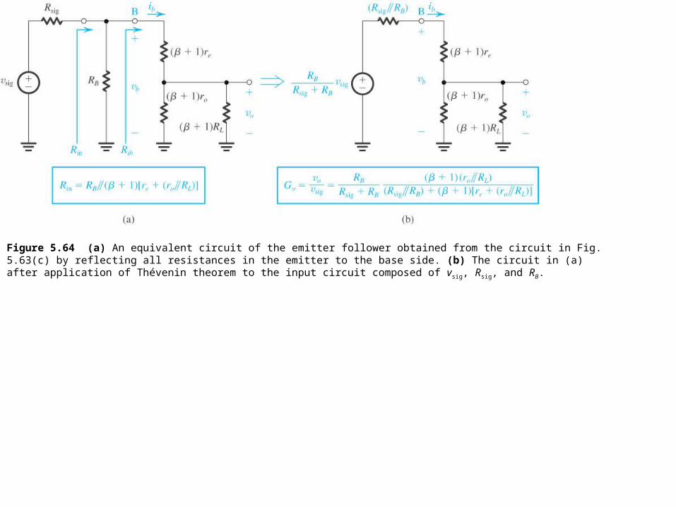
Figure 5.64 (a) An equivalent circuit of the emitter follower obtained from the circuit in Fig. 5.63(c) by reflecting all resistances in the emitter to the base side. (b) The circuit in (a) after application of Thévenin theorem to the input circuit composed of vsig, Rsig, and RB.

Figure 5.65 (a) An alternate equivalent circuit of the emitter follower obtained by reflecting all base-circuit resistances to the emitter side. (b) The circuit in (a) after application of Thévenin theorem to the input circuit composed of vsig, Rsig / ( 1 1), and RB / ( 1 1).

Figure 5.66 Thévenin equivalent circuit of the output of the emitter follower of Fig. 5.63(a). This circuit can be used to find vo and hence the overall voltage gain vo/vsig for any desired RL.

Table 5.6

Figure 5.67 The high-frequency hybrid- model.

Figure 5.68 Circuit for deriving an expression for hfe(s) ; Ic/Ib.
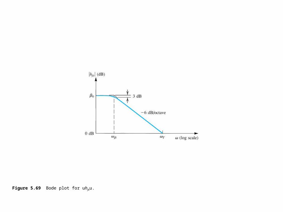
Figure 5.69 Bode plot for uhfeu.

Figure 5.70 Variation of fT with IC.

Table 5.7

Figure 5.71 (a) Capacitively coupled common-emitter amplifier. (b) Sketch of the magnitude of the gain of the CE amplifier versus frequency. The graph delineates the three frequency bands relevant to frequency-response determination.

Figure 5.72 Determining the high-frequency response of the CE amplifier: (a) equivalent circuit; (b) the circuit of (a) simplified at both the input side and the output side; (c) equivalent circuit with C replaced at the input side with the equivalent capacitance Ceq; (d) sketch of the frequency-response plot, which is that of a low-pass STC circuit.
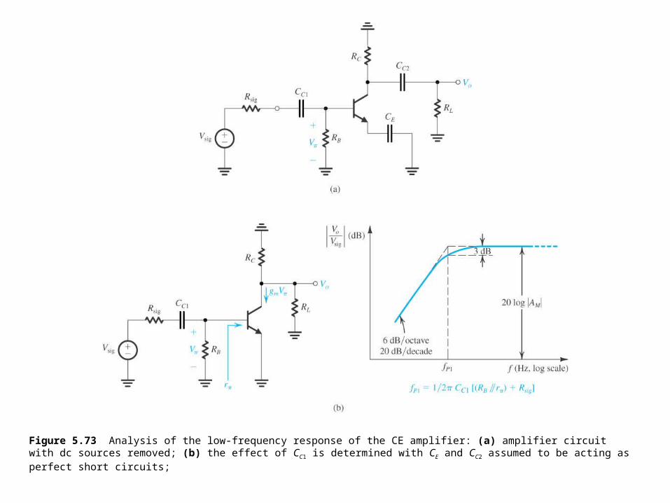
Figure 5.73 Analysis of the low-frequency response of the CE amplifier: (a) amplifier circuit with dc sources removed; (b) the effect of CC1 is determined with CE and CC2 assumed to be acting as perfect short circuits;

Figure 5.73 (Continued) (c) the effect of CE is determined with CC1 and CC2 assumed to be acting as perfect short circuits; (d) the effect of CC2 is determined with CC1 and CE assumed to be acting as perfect short circuits;

Figure 5.73 (Continued) (e) sketch of the low-frequency gain under the assumptions that CC1, CE, and CC2 do not interact and that their break (or pole) frequencies are widely separated.

Figure 5.74 Basic BJT digital logic inverter.
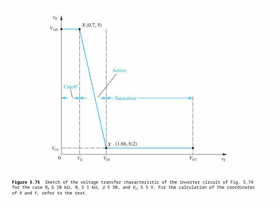
Figure 5.75 Sketch of the voltage transfer characteristic of the inverter circuit of Fig. 5.74 for the case RB 5 10 k, RC 5 1 k, 5 50, and VCC 5 5 V. For the calculation of the coordinates of X and Y, refer to the text.

Figure 5.76 The minority-carrier charge stored in the base of a saturated transistor can be divided into two components: That in blue produces the gradient that gives rise to the diffusion current across the base, and that in gray results from driving the transistor deeper into saturation.

Figure E5.53

Figure 5.77 The transport form of the Ebers-Moll model for an npn BJT.

Figure 5.78 The SPICE large-signal Ebers-Moll model for an npn BJT.

Figure 5.79 The PSpice testbench used to demonstrate the dependence of dc on the collector bias current IC for the Q2N3904 discrete BJT (Example 5.20).

Figure 5.80 Dependence of dc on IC (at VCE 5 2 V) in the Q2N3904 discrete BJT (Example 5.20).

Figure 5.81 Capture schematic of the CE amplifier in Example 5.21.

Figure 5.82 Frequency response of the CE amplifier in Example 5.21 with Rce = 0 and Rce = 130 .
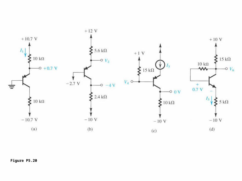
Figure P5.20

Figure P5.21

Figure P5.24

Figure P5.26
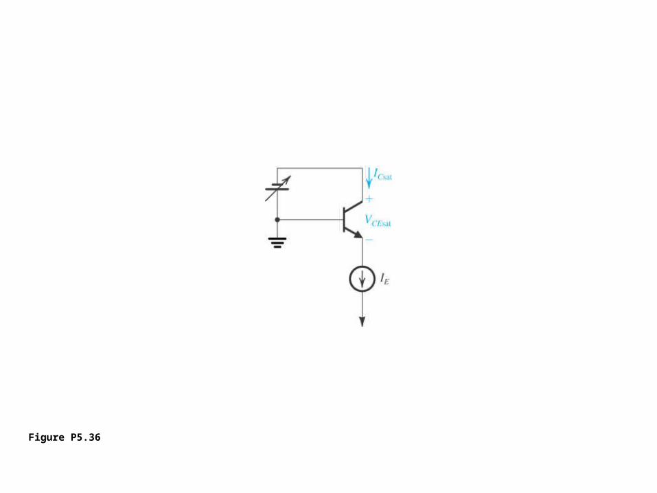
Figure P5.36

Figure P5.44

Figure P5.53
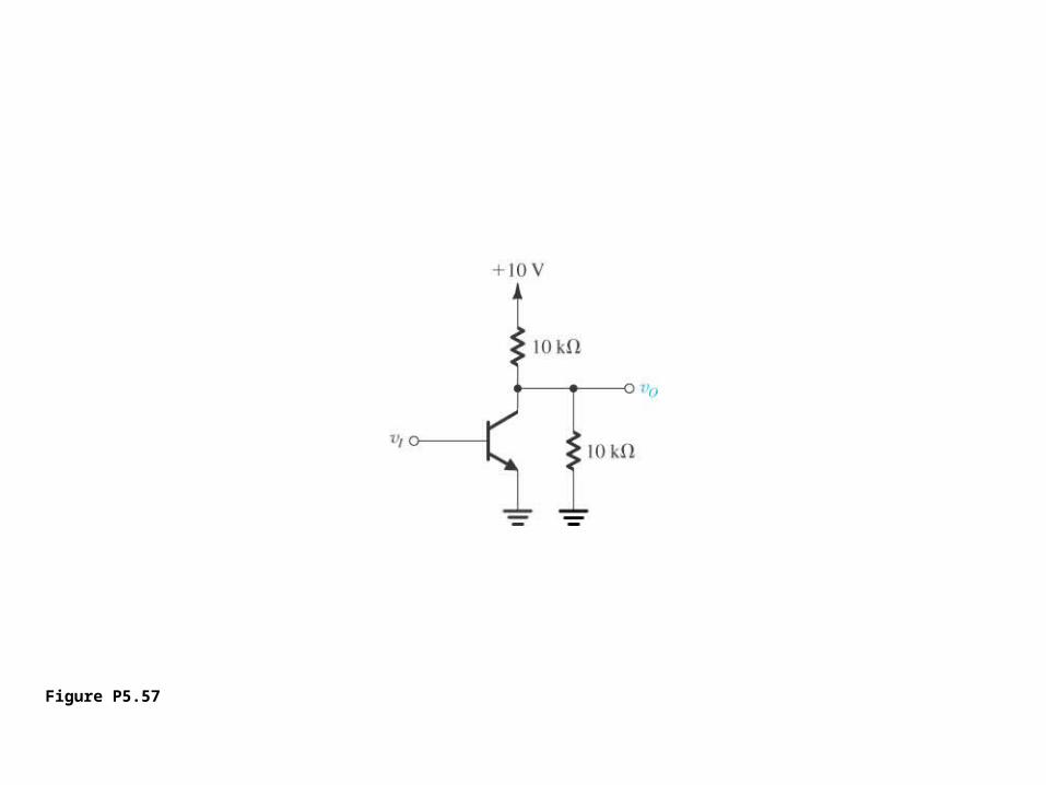
Figure P5.57

Figure P5.58

Figure P5.65

Figure P5.66

Figure P5.67

Figure P5.68

Figure P5.69

Figure P5.71

Figure P5.72
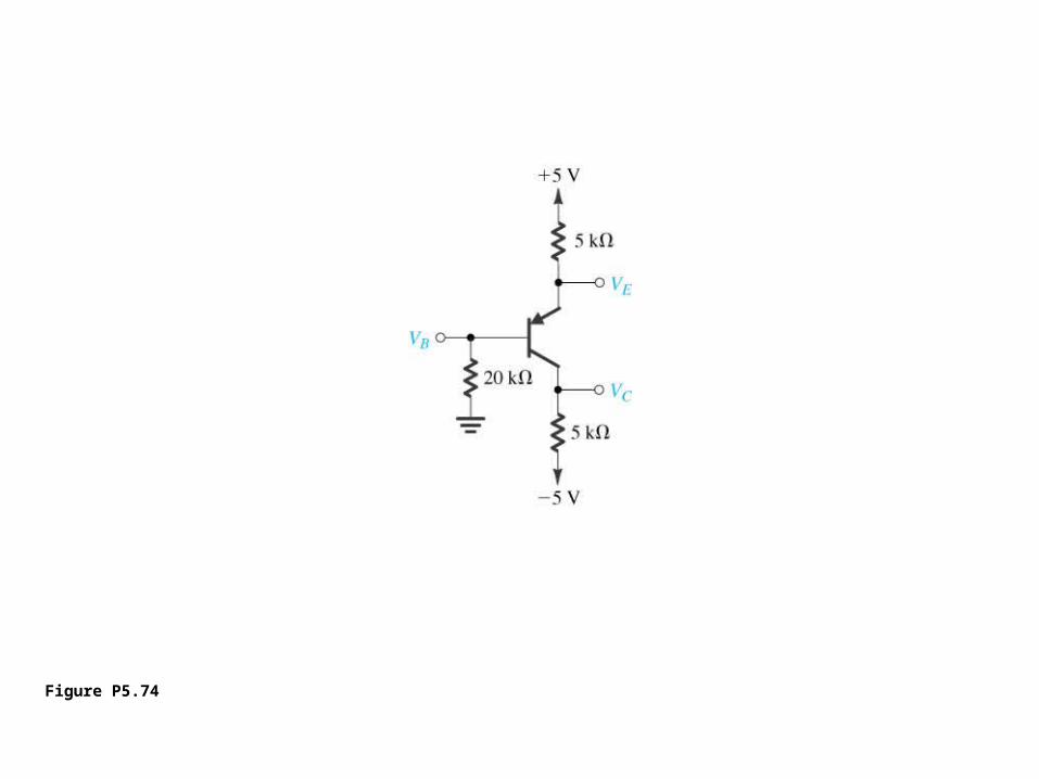
Figure P5.74

Figure P5.76

Figure P5.78
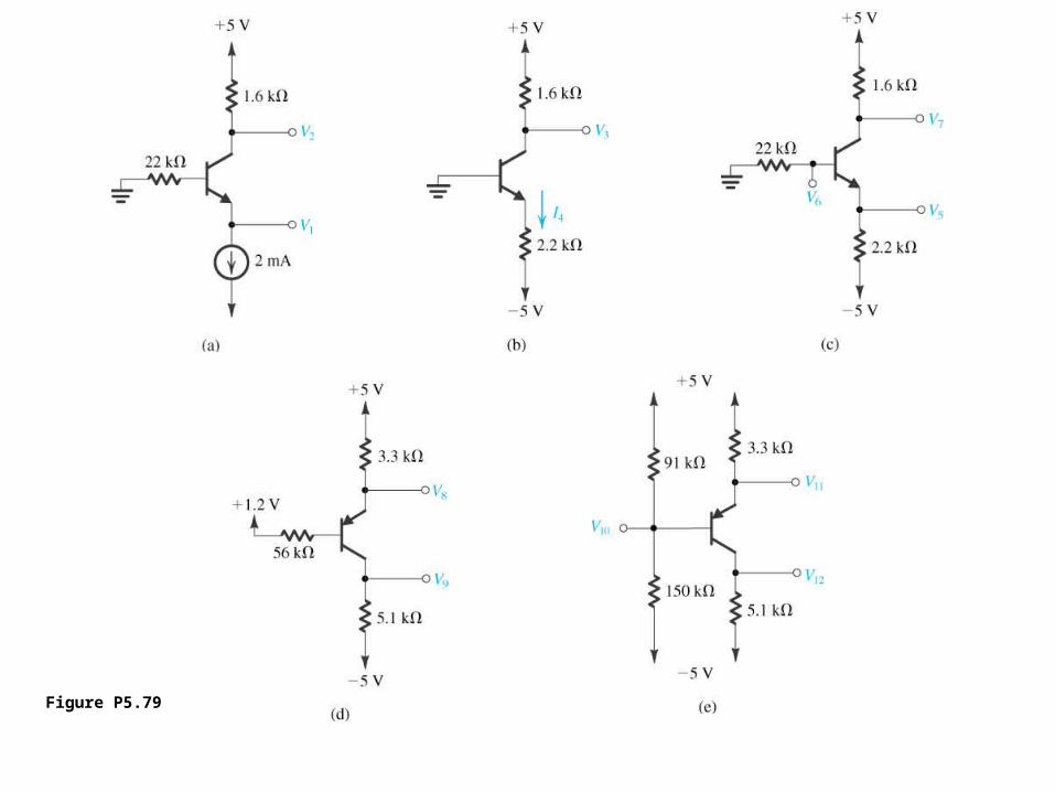
Figure P5.79
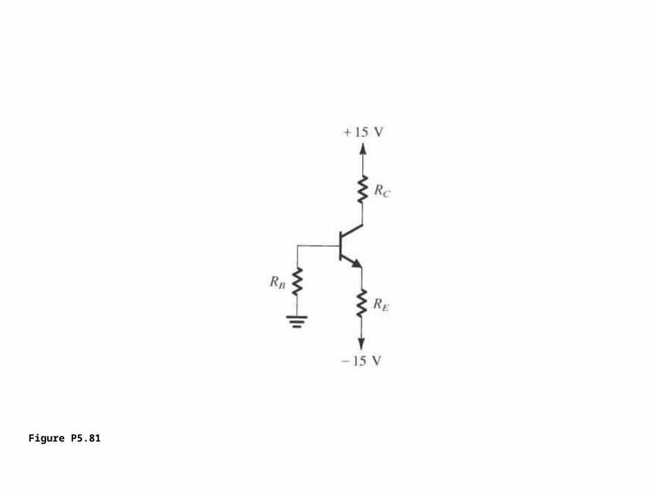
Figure P5.81

Figure P5.82

Figure P5.83
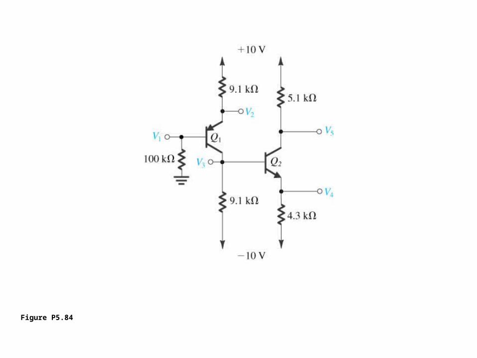
Figure P5.84

Figure P5.85

Figure P5.86
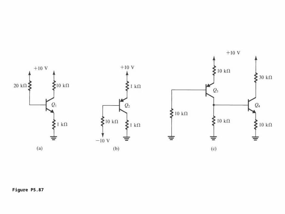
Figure P5.87

Figure P5.96

Figure P5.97
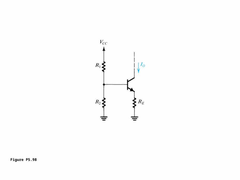
Figure P5.98

Figure P5.99

Figure P5.100

Figure P5.101

Figure P5.112

Figure P5.115

Figure P5.116

Figure P5.124
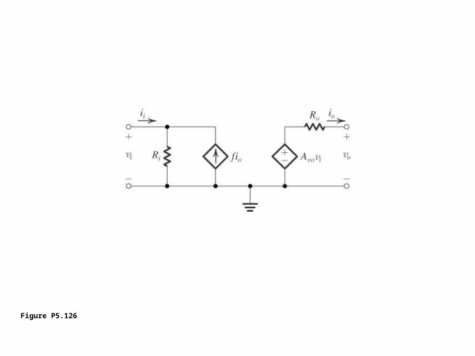
Figure P5.126

Figure P5.130
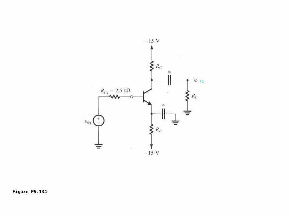
Figure P5.134

Figure P5.135

Figure P5.136

Figure P5.137
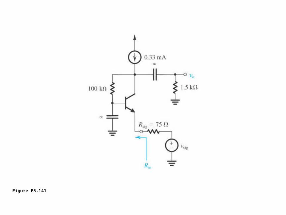
Figure P5.141

Figure P5.143

Figure P5.144

Figure P5.147

Figure P5.148

Figure P5.159

Figure P5.161

Figure P5.162
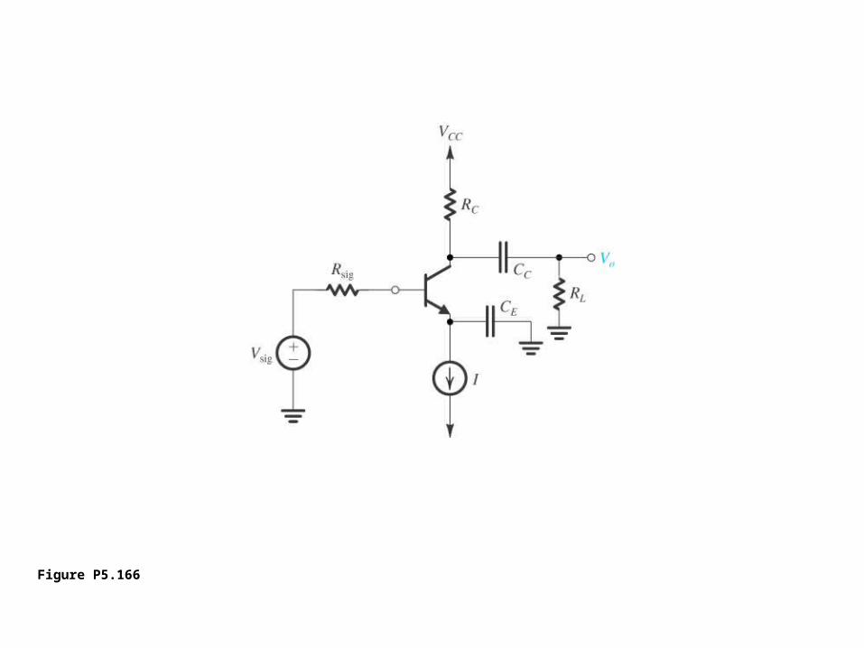
Figure P5.166

Figure P5.167

Figure P5.171
Related Documents