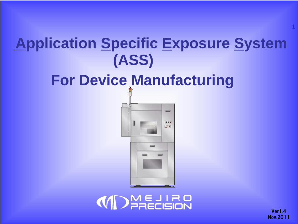
1 Ver1.4 Nov.2011 A pplication S pecific E xposure S ystem (ASS) For Device Manufacturing

Welcome message from author
This document is posted to help you gain knowledge. Please leave a comment to let me know what you think about it! Share it to your friends and learn new things together.
Transcript
1
Ver1.4 Nov.2011
Application Specific Exposure System(ASS)
For Device Manufacturing

2(Contents)
1.Introduction of Mejiro Precision,Inc.
2.General Market Trend and Overview of Mejiro Stepper
3.Introduction of Application Specific Exposure System (ASS)
4.Strategy for Device Production
5.3D Lithography by ASS

3(Contents)
1.Introduction of Mejiro Precision,Inc.
2.General Market Trend and Overview of Mejiro Stepper
3.Introduction of Application Specific Exposure System (ASS)
4.Strategy for Device Production

4
Company overviewMejiro Precision Confidential
・Activities Design, research and development of optical system・Employees 40
Mejiro Precision aims at Fab-less Company.
The main business is research & development, and manufacturing has been consigned to the external cooperation company.
5
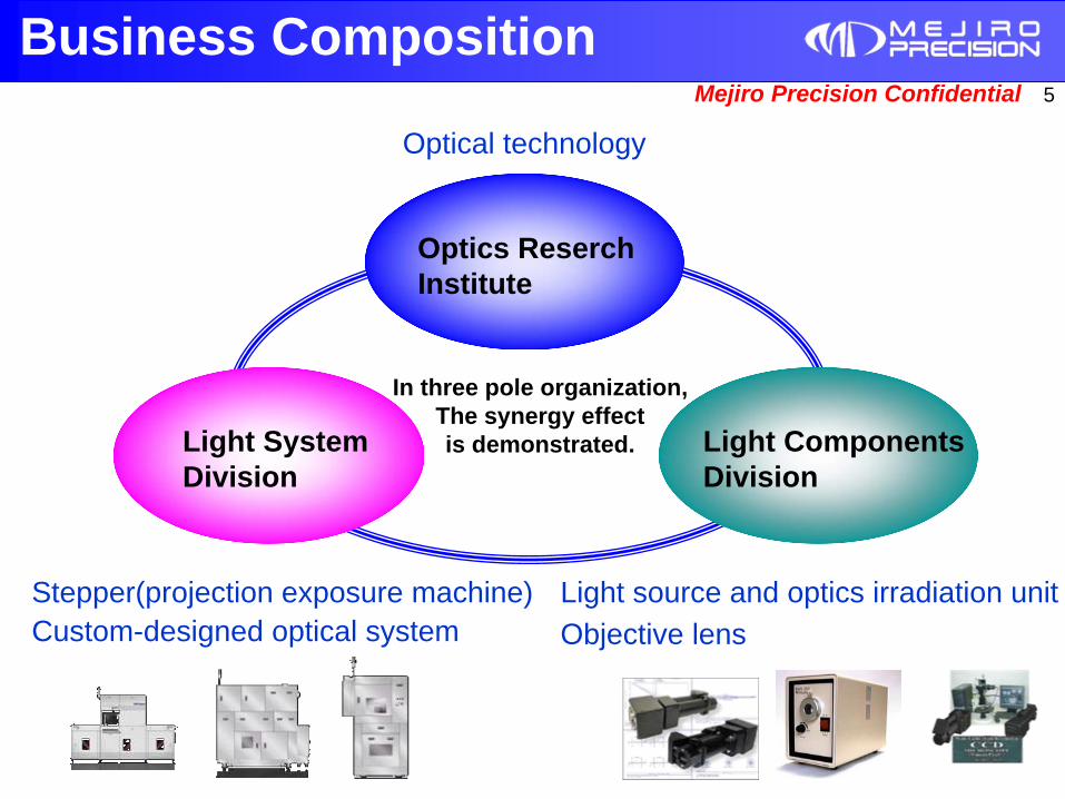
Business CompositionMejiro Precision Confidential
In three pole organization,The synergy effectis demonstrated.
Optics Reserch Institute
Light System Division
Light Components Division
Stepper(projection exposure machine)Custom-designed optical system
Light source and optics irradiation unitObjective lens
Optical technology
6
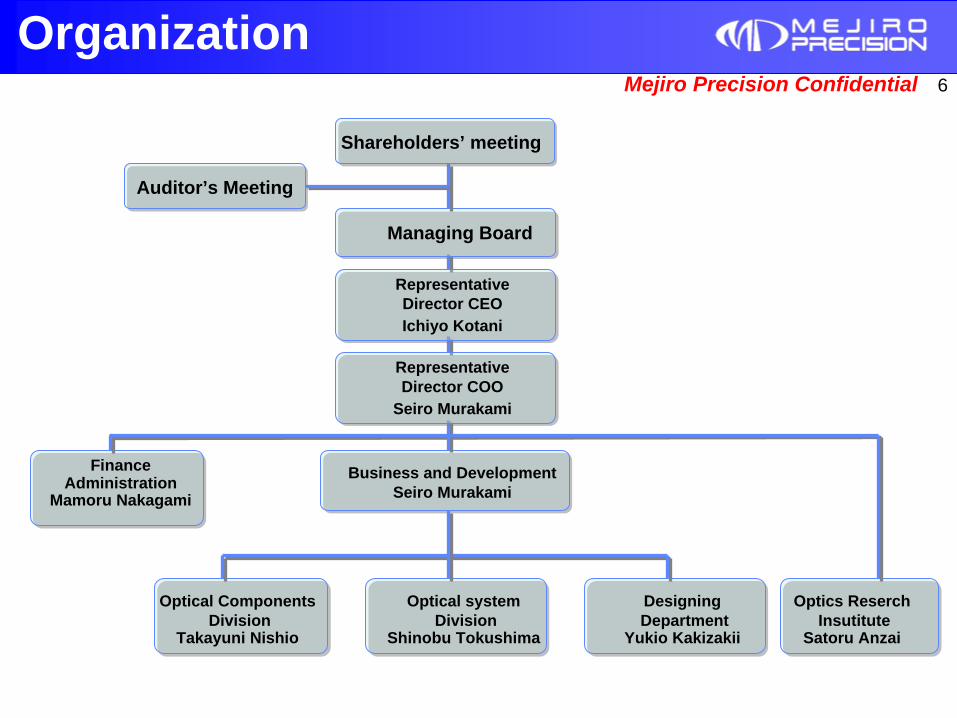
OrganizationMejiro Precision Confidential
Shareholders’ meeting
Managing Board
RepresentativeDirector CEOIchiyo Kotani
Business and DevelopmentSeiro Murakami
Auditor’s Meeting
RepresentativeDirector COO
Seiro Murakami
Optics ReserchInsutitute
Satoru Anzai
Optical systemDivision
Shinobu Tokushima
Optical ComponentsDivision
Takayuni Nishio
FinanceAdministration
Mamoru Nakagami
DesigningDepartment
Yukio Kakizakii

7(Contents)
1.Introduction of Mejiro Precision,Inc.
2.General Market Trend and Overview of Mejiro Stepper
3.Introduction of Application Specific Exposure System (ASS)
4.Strategy for Device Production
8
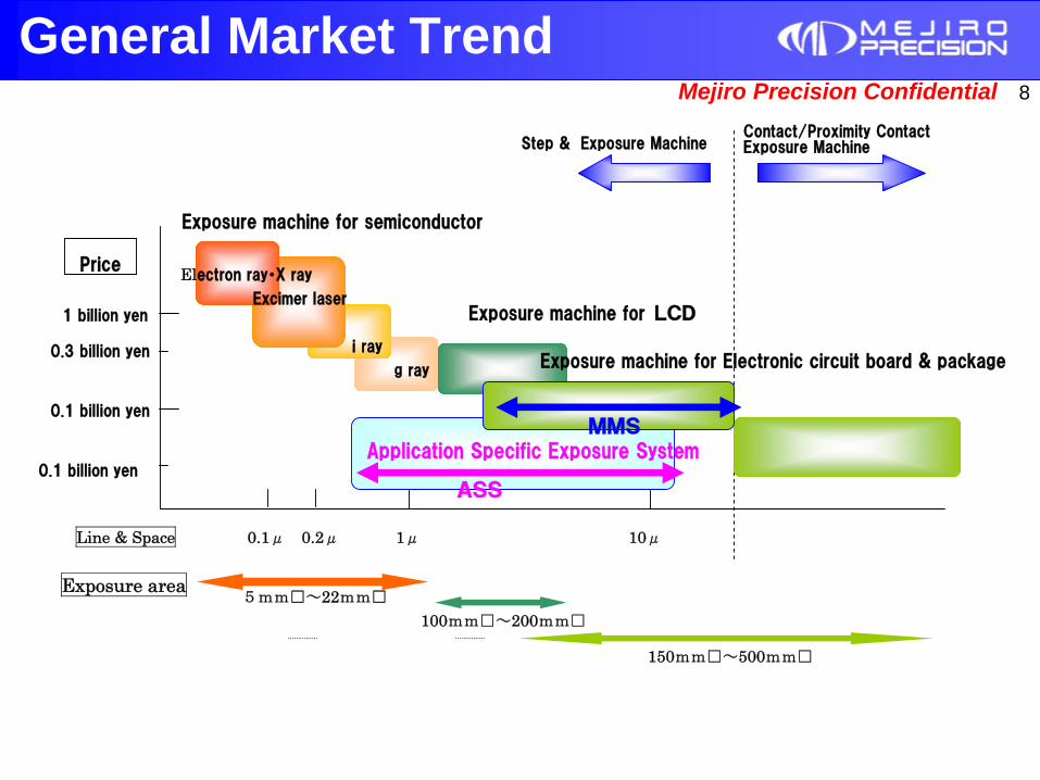
General Market TrendMejiro Precision Confidential
Electron ray・X ray
Excimer laser
i ray
g ray
Line & Space 0.1μ 0.2μ 1μ 10μ
Exposure area
Exposure machine for Electronic circuit board & package
Exposure machine for semiconductor
Exposure machine for LCD
5mm□~22mm□
100mm□~200mm□
150mm□~500mm□
Contact/Proximity ContactExposure Machine Step & Exposure Machine
1 billion yen
Price
0.3 billion yen
0.1 billion yen
0.1 billion yen
MMS
ASS
Application Specific Exposure System
9
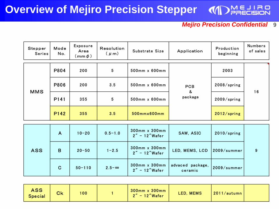
Overview of Mejiro Precision StepperMejiro Precision Confidential
Stepper Ser ies
Mode No.
ExposureArea
(mmφ)
Resolution(μm)
Substrate Size ApplicationProduct ion beginn ing
Numbers of sales
P804 200 5 500mm x 600mm 2003
P806 200 3 .5 500mm x 600mm 2008/spr ing
P141 355 5 500mm x 600mm 2009/spr ing
P142 355 3 .5 500mmx600mm 2012/spr ing
A 10-20 0 .5-1 .0300mm x 300mm2" - 12"Wafer
SAW, ASIC 2010/spr ing
B 20-50 1-2 .5300mm x 300mm2" - 12"Wafer
LED, MEMS, LCD 2009/summer
C 50-110 2 .5-∞300mm x 300mm2" - 12"Wafer
advaced package ,ceramic
2009/summer
ASSSpecial
Ck 100 1300mm x 300mm2" - 12"Wafer
LED, MEMS 2011/autumn
ASS
MMS 16PCB &
package
9
10(Contents)
1.Introduction of Mejiro Precision,Inc.
2.General Market Trend and Overview of Mejiro Stepper
3.Introduction of Application Specific Exposure System (ASS)
4.Strategy for Device Production

11
Introduction of ASSMejiro Precision Confidential
・
Concept
・
Achievement of Wide Exposure Specification
・
Practicable Productivity
・
Module Concept for High Cost Performance
・
Back-Side Alignment
・
Substrate Holder
・
Edge Blind Mechanism
・
Small and lightweight
・Introduction of ASS(Application Specific Exposure System)
12
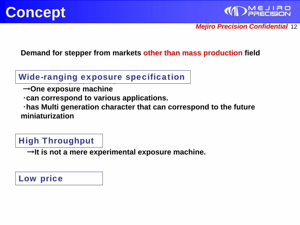
ConceptMejiro Precision Confidential
Demand for stepper from markets other than mass production field
・Wide-ranging exposure specification→One exposure machine・can correspond to various applications. ・has Multi generation character that can correspond to the future miniaturization
・High Throughput→It is not a mere experimental exposure machine.
・Low price
Wide-ranging exposure specification
High Throughput
Low price

13
Achievement of Wide Exposure SpecificationMejiro Precision Confidential
NA is large. (high resolving power)
NA is small(low resolving power)
Exposure area is small Exposure area is large
Open NA aperture Squeeze NA aperture.
1-1
Introduction of NA changeable mechanism

14
Achievement of Wide Exposure SpecificationMejiro Precision Confidential
Lens Series and Application Range
120
110
100
90
80
70
60
50
40
30
20
10
0
Resolving power(μm)
4μm
110mmΦ
1μm
20mmΦ0.5μm
10mmΦ
Exposure
fie
ld (
dia
mete
r, m
m)
Lens A Lens B Lens C
2.5μm
50mmΦ
5
SAW
LED
Ceramic
LCD
MEMS
Th in film
magne t ic
heads
Elec tron ic
c irc u it board
& package
1 0.5
ASIC
Lens Ck
1-2
Continuously Covered with Three Kinds of Lenses
15
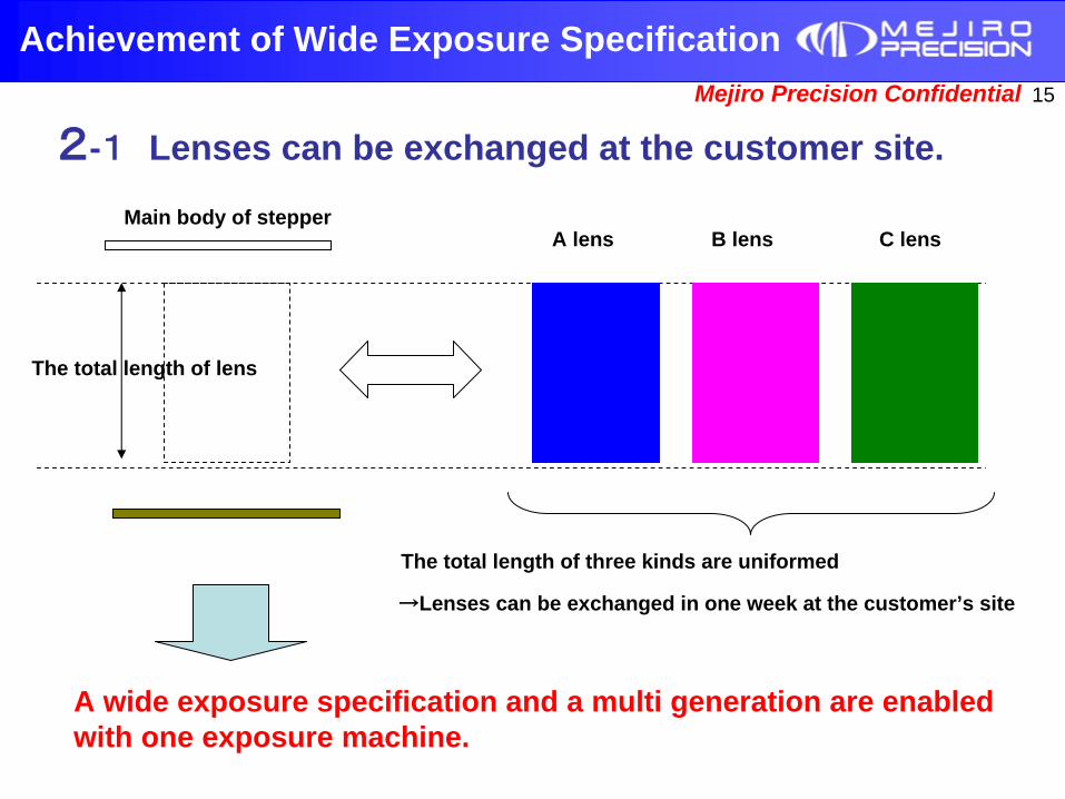
Achievement of Wide Exposure SpecificationMejiro Precision Confidential
A lens B lens C lens
The total length of lens
The total length of three kinds are uniformed
Main body of stepper
→Lenses can be exchanged in one week at the customer’s site
A wide exposure specification and a multi generation are enabled with one exposure machine.
2-1
Lenses can be exchanged at the customer site.

16
Achievement of Wide Exposure SpecificationMejiro Precision Confidential
Lens B Lens A
Projection Flame Main Body
• Easy exchange on customer’s site
• Short period work schedule
• Mejiro’s engineer can change the lens on customer’s manufacturing area.
→
Changing lens and Readjust within 1 week ,and checking within 0.5 week.
2-2
Lenses Exchange mechanism

17
Practicable ProductivityMejiro Precision Confidential
The technology of stepper (MMS) for electronic circuit board and the package mass production was applied as it was.
・Small size and lightweight X/Y stage( 300mmx300mm 12” stroke capability )
・Optical system of high illumination
・Real-time AF mechanism
・Global alignment function
High throughput ( 30 second / 12 "Wafer substrate)
→A small-scale production line can be constructed.
High Throughput

18
Module Concept for High Cost PerformanceMejiro Precision Confidential
ASS stepper is composed of a lot of independent functional elements
(more than 50 kinds of modules).
Illumination optics
Lamp
Reticle system
Projection lens
Substrate stage
Substrate transfer system
Reticle change system
An individual module corresponds to all the possible function variations with the possibility that the customer uses it.
The module can be assumed that all are optional, and be selected.
modular framework
The minimum requirement can be composed for the customer.
High Cost Performance
Module Concept

19
Back Side AlignmentMejiro Precision Confidential
Surface alignment
AlignmentMicroscope
Prism by return
Back side alignment
Alignment mark
Back Side mark

20
Substrate HolderMejiro Precision Confidential
Vacuum by
Sponge type material(多孔質)
→
Soft vacuum contact by innumerable air hole
Peripheral Cramp Skirt
Stage Holder for substrate
Flatness is secured without damaging the substrate.
Substrate
21
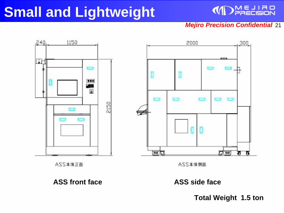
Small and LightweightMejiro Precision Confidential
ASS front face ASS side face
Total Weight 1.5 ton

22(Contents)
1.Introduction of Mejiro Precision,Inc.
2.General Market Trend and Overview of Mejiro Stepper
3.Introduction of Application Specific Exposure System (ASS)
4.Strategy for Device Production

23
Strategy for Device ProductionMejiro Precision Confidential
Strategy for Device Production
1. Advanced Technologyfor Enhanced Resolution
2. Lithography Roadmap & Mejiro Strategy
24
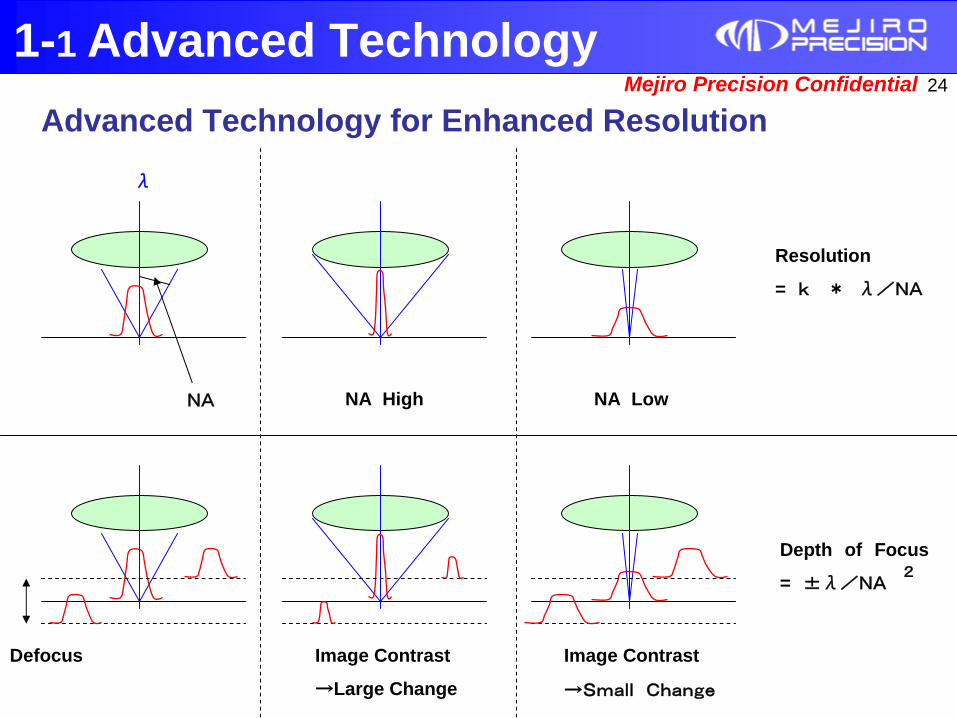
1-1 Advanced TechnologyMejiro Precision Confidential
Resolution
= k
*
λ/NA
λ
NA
Depth of Focus
= ±λ/NA2
Defocus
NA High NA Low
Image Contrast
→Large Change
Image Contrast
→Small
Change
Advanced Technology for Enhanced Resolution

25
1-2 Advanced TechnologyMejiro Precision Confidential
Higher NA lens can resolve critical dimension pattern, but reduces focus depth rapidly.
When high NA is used for the rough pattern, the focus depth becomes shallow.
In the rough pattern, large DOF can be obtained by lower NA according to pattern size.
・Fine IC,LSI(DRAM, CPU Logic, etc)
Super Flat(≤1μm)
→
No DOF Requirement
→
Larger NA →
Finer Pattern
・Package, Bump, LED, Ceramic, MEMS….
Large凸凹(10~100~500μm)
→
Large DOF Requirement
→
Optimum NA → Maximum DOF
26
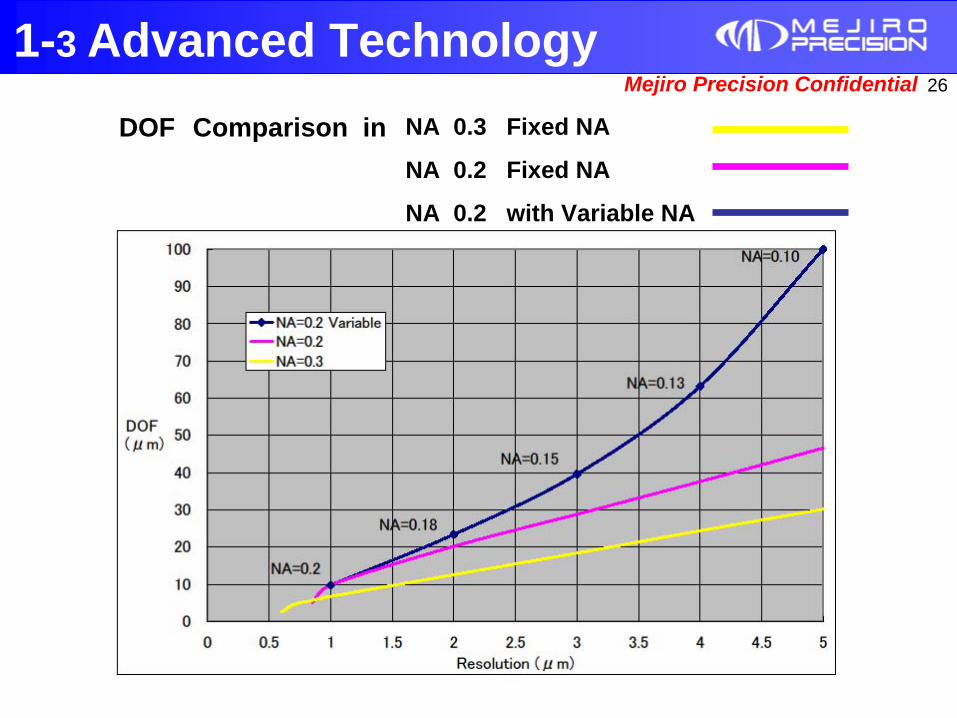
1-3 Advanced TechnologyMejiro Precision Confidential
DOF Comparison in NA 0.3 Fixed NA
NA 0.2 Fixed NA
NA 0.2 with Variable NA

27
1-4 Advanced TechnologyMejiro Precision Confidential
・Introduction of Variable NA Optics enables to obtain best resolving power (maximum DOF) at various pattern size.
・Sub-micron pattern generation
1~0.8μm
→
Resolution Enhancement technology (RET) can
enable much higher resolution and depth of focus.
ASS stepper can introduce Annular Illumination as RET.By Annular Illumination introduction、DOF increase is 20-30% compared to conventional illumination in optimum condition.
≤
0.8μm
→
It is possible to correspond to 0.5μm pattern by
exchanging for A lens.
・As a result, deep focus depth can be secured in each generation of device manufacturing.

28Mejiro Precision Confidential2. Lithography Roadmap & Mejiro Strategy
≥ 2μm 1~2μm 0.2~1μm 0.2μm
≥
Gap
Aligner
Contact
Aligner
Low
end
stepper
High
end
stepper
General
Trend
Mejiro
Strategy
Single ASS
machine for Multiple Lithgraphy generations
B Lens + Variable
NA
B Lens + RET(Annular illumination)
Replace from B
Lens to
A
Lens
29
3D lithography by ASS stepper
September, 2011
Mejiro Precision Confidential
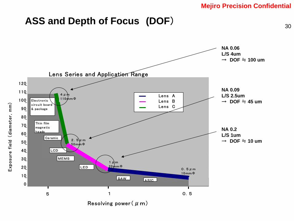
30
Lens Series and Application Range
120
110
100
90
80
70
60
50
40
30
20
10
0
Resolving power(μm)
4μm
110mmΦ
1μm
20mmΦ0.5μm
10mmΦ
Exposure
fie
ld (
dia
mete
r, m
m)
Lens A Lens B Lens C
2.5μm
50mmΦ
5
SAW
LED
Ceramic
LCD
MEMS
Th in film
magne t ic
heads
Ele c tron ic
c ircu it board
& package
1 0.5
ASIC
NA 0.06L/S 4um→
DOF ≒ 100 um
NA 0.09L/S 2.5um→
DOF ≒ 45 um
NA 0.2L/S 1um→
DOF ≒ 10 um
ASS and Depth of Focus (DOF)
Mejiro Precision Confidential

31Basic concept
+1st Diffracted light
The 0th light
Resolution Limit
-1st Diffracted light
Non-resolved pattern
Mejiro Precision Confidential

32Control of reticle transmittance ratio
by non-resolved dot pattern
80% 90%
Intensity 64% 81%
1um□ non-resolved dotArea 50um2
Transmittance
Mejiro Precision Confidential
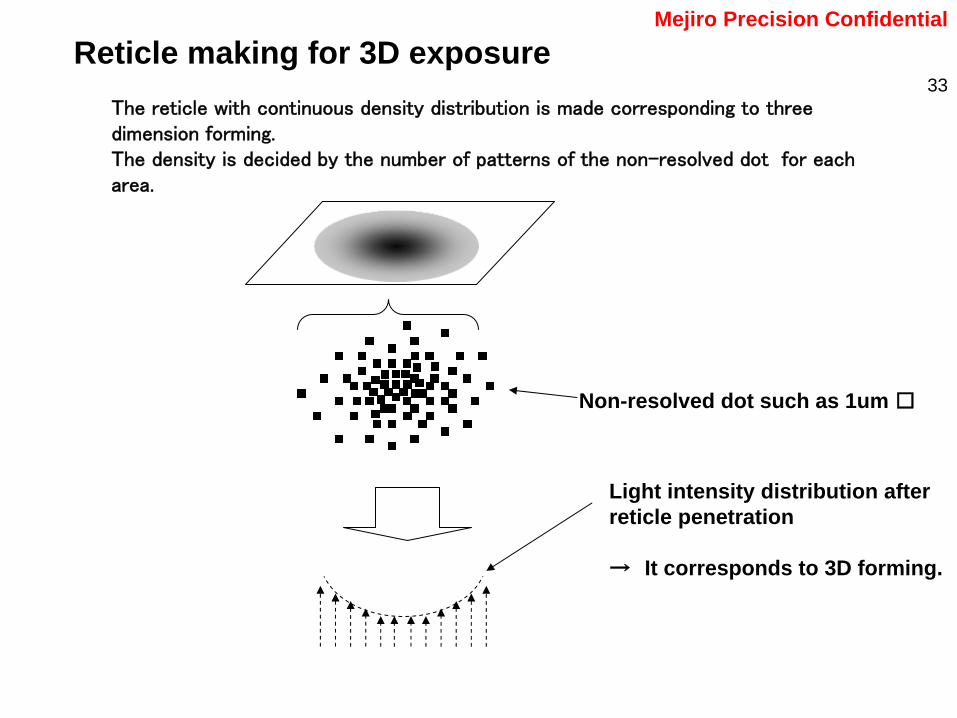
33Reticle making for 3D exposure
The reticle
with continuous density distribution is made corresponding to three dimension forming. The density is decided by the number of patterns of the non-resolved dot for each area.
Light intensity distribution after reticle penetration
→
It corresponds to 3D forming.
Non-resolved dot such as 1um □
Mejiro Precision Confidential

34
The relation between absorption energy (E) by the exposure and resist dissolution depth (Z) are experimentally decided.
Resist thickness
E1 E 2 E 3 ・・・・
Z 1 Z 2 Z3
zZ3 Z 2 Z1
E1
E2E3
Dissolution depth function Z = D (E) is decided.
→E(Z) corresponding to dissolution depth Z is calculated.
E(Z) = D (Z)
Emin.
-1
Plot
E
Absorption energy and resist dissolution depthMejiro Precision Confidential

35Actual
Result
for
Micro
Lens
Array
Without thickness correction With thickness correctionby dissolution depth function Z = D (E)
Mejiro Precision Confidential

36
Presentation is ended above. Thank you for listening.
Related Documents
![[SEMI Theater] Taiwan Market Update SEMICON Taiwan](https://static.cupdf.com/doc/110x72/55588b1ad8b42a5d328b52fd/semi-theater-taiwan-market-update-semicon-taiwan.jpg)