1356 IEEE TRANSACTIONS ON POWER ELECTRONICS, VOL. 30, NO. 3, MARCH 2015 Low-Volume PFC Rectifier Based on Nonsymmetric Multilevel Boost Converter Behzad Mahdavikhah, Senior Member, IEEE, and Aleksandar Prodi´ c, Member, IEEE Abstract—This paper introduces a digitally controlled single- phase rectifier with power factor correction (PFC) based on a modified three-level boost converter topology. In comparison with the conventional boost-based systems, the new PFC rectifier has about three times smaller inductor and significantly lower switch- ing losses. The improvements are achieved by replacing the out- put capacitor of the boost converter with a nonsymmetric active capacitive divider, with a 3:1 division ratio, and by utilizing the downstream converter stage for the capacitive divider’s center-tap voltage regulation. The nonsymmetric voltage divider and applied switching sequence effectively provide four-level converter behav- ior using the same number of components as three-level converters. As a result, a 66% reduction of the inductor compared to the con- ventional boost-based PFC and a 33% compared to the standard three-level solutions operating at the same effective switching fre- quencies are also achieved. Experimental results obtained with a 400 W, 200 kHz, universal input voltage (85 V rms –265 V rms ) PFC prototype demonstrate three times smaller inductor current ripple than that of the conventional boost converter allowing for the same inductor reduction. Efficiency improvements of up to a 6% are also demonstrated. Index Terms—AC-DC converters, boost converter, multilevel converters, power factor correction (PFC). I. INTRODUCTION T HE boost converter operating in continuous current mode (CCM) followed by an isolated dc–dc converter [1], [2] is among the most widely used configurations in single-phase rectifiers with power factor correction (PFC). This is mostly due to the continuous input current of the boost stage reducing electromagnetic interference (EMI) filtering requirements and fairly simple controller implementation [2]–[5]. This topology is used in a wide range of applications requiring between 100 and 500 W of power. Some examples include laptop and personal computers, monitors, communication equipment, TV sets, and other consumer electronics. One of the major drawbacks of the boost-based front stage is a relatively large size of the inductor limiting its use in weight and Manuscript received October 5, 2013; revised December 19, 2013 and Febru- ary 18, 2014; accepted March 28, 2014. Date of publication April 24, 2014; date of current version October 15, 2014. This paper was presented in part at the IEEE APEC 2013 Conference and Exhibition, Long Beach, CA, USA. Recom- mended for publication by Associate Editor Y.-M. Chen. The authors are with the Laboratory for Power Management and In- tegrated Switch-Mode Power Supplies ECE Department, University of Toronto 10 King’s College Road, Toronto, ON M5S 3G4 Canada (e-mail: [email protected]; [email protected]). Color versions of one or more of the figures in this paper are available online at http://ieeexplore.ieee.org. Digital Object Identifier 10.1109/TPEL.2014.2317723 volume sensitive applications. The large inductor also causes nonnegligible core losses [5], [6] and results in a relatively large parasitic capacitance of the winding introducing high- frequency noise [7]. The conventional boost-based topologies also suffer from problems related to switching losses [2], [8], causing heat dissipation, whose handling often requires bulky cooling components. The switching losses are mostly related to the operation of the transistor and the diode at the relatively high output, i.e., bus, voltage, which for the universal input (85 V rms to 265 V rms ) boost PFCs it is usually about 400 V. To minimize the size of the boost-based PFC system in- ductors, a number of methods have been proposed in the past [5]–[15]. Those can generally be divided into frequency- increase-based and topological changes. Interleaved topologies [13]–[15], which reduce the inductor by effectively increasing the switching frequency, have proven to be effective solutions for larger power ratings, where the semi- conductor switching components can be fully utilized. However, these solutions still suffer from relatively high switching losses and, when operating at light and medium loads, from either degradation of efficiency or quality of the input current wave- form [16]. The topological methods [5]–[11], minimize both the inductor value and the switching losses, by reducing the stress of the components. In the flying capacitor multicell boost [7], derived from the multilevel concepts [12], these advantages are achieved by adding few switches and a relatively large flying capacitor. A three-level boost-based PFC [6] replaces the output capacitor of the boost converter with a compact active capacitive divider and, for the same switching frequency, results in a 50% reduction of the inductor value compared to the conventional boost-based solutions. The main goal of this paper is to introduce a novel single- phase multilevel boost-based PFC rectifier that allows fur- ther reduction of the inductor volume while maintaining the benefits of the previously presented multilevel solutions. The new converter, named nonsymmetric multilevel boost (NSMB), and its digital controller are shown in Fig. 1. The system is primarily designed for the previously mentioned applica- tions ranging between 100 and 500 W. The new topology reduces the size of the boost inductor to a one-third of the value required for the conventional boost PFC using the same number and volume of components as the three-level flying- capacitor-less-divider-based solution [6]. In essence, utilizing similar hardware as a three-level converter, the introduced topol- ogy operates as a four-level converter. This results in the im- provements similar to those obtained by moving from a con- ventional two-level boost to a three-level topology without 0885-8993 © 2014 IEEE. Translations and content mining are permitted for academic research only. Personal use is also permitted, but republication/redistribution requires IEEE permission. See http://www.ieee.org/publications standards/publications/rights/index.html for more information.

Welcome message from author
This document is posted to help you gain knowledge. Please leave a comment to let me know what you think about it! Share it to your friends and learn new things together.
Transcript
1356 IEEE TRANSACTIONS ON POWER ELECTRONICS, VOL. 30, NO. 3, MARCH 2015
Low-Volume PFC Rectifier Based on NonsymmetricMultilevel Boost Converter
Behzad Mahdavikhah, Senior Member, IEEE, and Aleksandar Prodic, Member, IEEE
Abstract—This paper introduces a digitally controlled single-phase rectifier with power factor correction (PFC) based on amodified three-level boost converter topology. In comparison withthe conventional boost-based systems, the new PFC rectifier hasabout three times smaller inductor and significantly lower switch-ing losses. The improvements are achieved by replacing the out-put capacitor of the boost converter with a nonsymmetric activecapacitive divider, with a 3:1 division ratio, and by utilizing thedownstream converter stage for the capacitive divider’s center-tapvoltage regulation. The nonsymmetric voltage divider and appliedswitching sequence effectively provide four-level converter behav-ior using the same number of components as three-level converters.As a result, a 66% reduction of the inductor compared to the con-ventional boost-based PFC and a 33% compared to the standardthree-level solutions operating at the same effective switching fre-quencies are also achieved. Experimental results obtained with a400 W, 200 kHz, universal input voltage (85 Vrms–265 Vrms)PFC prototype demonstrate three times smaller inductor currentripple than that of the conventional boost converter allowing forthe same inductor reduction. Efficiency improvements of up to a6% are also demonstrated.
Index Terms—AC-DC converters, boost converter, multilevelconverters, power factor correction (PFC).
I. INTRODUCTION
THE boost converter operating in continuous current mode(CCM) followed by an isolated dc–dc converter [1], [2]
is among the most widely used configurations in single-phaserectifiers with power factor correction (PFC). This is mostlydue to the continuous input current of the boost stage reducingelectromagnetic interference (EMI) filtering requirements andfairly simple controller implementation [2]–[5]. This topology isused in a wide range of applications requiring between 100 and500 W of power. Some examples include laptop and personalcomputers, monitors, communication equipment, TV sets, andother consumer electronics.
One of the major drawbacks of the boost-based front stage is arelatively large size of the inductor limiting its use in weight and
Manuscript received October 5, 2013; revised December 19, 2013 and Febru-ary 18, 2014; accepted March 28, 2014. Date of publication April 24, 2014; dateof current version October 15, 2014. This paper was presented in part at theIEEE APEC 2013 Conference and Exhibition, Long Beach, CA, USA. Recom-mended for publication by Associate Editor Y.-M. Chen.
The authors are with the Laboratory for Power Management and In-tegrated Switch-Mode Power Supplies ECE Department, University ofToronto 10 King’s College Road, Toronto, ON M5S 3G4 Canada (e-mail:[email protected]; [email protected]).
Color versions of one or more of the figures in this paper are available onlineat http://ieeexplore.ieee.org.
Digital Object Identifier 10.1109/TPEL.2014.2317723
volume sensitive applications. The large inductor also causesnonnegligible core losses [5], [6] and results in a relativelylarge parasitic capacitance of the winding introducing high-frequency noise [7]. The conventional boost-based topologiesalso suffer from problems related to switching losses [2], [8],causing heat dissipation, whose handling often requires bulkycooling components. The switching losses are mostly related tothe operation of the transistor and the diode at the relatively highoutput, i.e., bus, voltage, which for the universal input (85 Vrmsto 265 Vrms) boost PFCs it is usually about 400 V.
To minimize the size of the boost-based PFC system in-ductors, a number of methods have been proposed in thepast [5]–[15]. Those can generally be divided into frequency-increase-based and topological changes.
Interleaved topologies [13]–[15], which reduce the inductorby effectively increasing the switching frequency, have provento be effective solutions for larger power ratings, where the semi-conductor switching components can be fully utilized. However,these solutions still suffer from relatively high switching lossesand, when operating at light and medium loads, from eitherdegradation of efficiency or quality of the input current wave-form [16].
The topological methods [5]–[11], minimize both the inductorvalue and the switching losses, by reducing the stress of thecomponents. In the flying capacitor multicell boost [7], derivedfrom the multilevel concepts [12], these advantages are achievedby adding few switches and a relatively large flying capacitor. Athree-level boost-based PFC [6] replaces the output capacitor ofthe boost converter with a compact active capacitive divider and,for the same switching frequency, results in a 50% reduction ofthe inductor value compared to the conventional boost-basedsolutions.
The main goal of this paper is to introduce a novel single-phase multilevel boost-based PFC rectifier that allows fur-ther reduction of the inductor volume while maintaining thebenefits of the previously presented multilevel solutions. Thenew converter, named nonsymmetric multilevel boost (NSMB),and its digital controller are shown in Fig. 1. The systemis primarily designed for the previously mentioned applica-tions ranging between 100 and 500 W. The new topologyreduces the size of the boost inductor to a one-third of thevalue required for the conventional boost PFC using the samenumber and volume of components as the three-level flying-capacitor-less-divider-based solution [6]. In essence, utilizingsimilar hardware as a three-level converter, the introduced topol-ogy operates as a four-level converter. This results in the im-provements similar to those obtained by moving from a con-ventional two-level boost to a three-level topology without
0885-8993 © 2014 IEEE. Translations and content mining are permitted for academic research only. Personal use is also permitted, but republication/redistributionrequires IEEE permission. See http://www.ieee.org/publications standards/publications/rights/index.html for more information.
MAHDAVIKHAH AND PRODIC: LOW-VOLUME PFC RECTIFIER BASED ON NONSYMMETRIC MULTILEVEL BOOST CONVERTER 1357
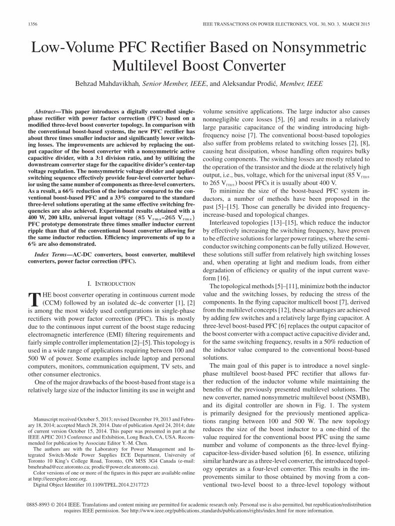
Fig. 1. NSMB-based PFC rectifier and its downstream stage.
increasing hardware complexity. Like other multilevel solutionsthe NSMB also reduces the switching losses and componentsvoltage stress. The new topology is also well suited to be usedwith efficiency optimization methods and techniques developedfor conventional boost-based topologies [17]–[21], allowing alladvantages of the previously developed methods to be utilizedhere as well.
The inductor reduction is achieved by providing nonequalvoltages across the capacitive divider cells, through a capacitordivider with a 3:1 conversion ratio, and applying a switchingscheme that results in four inductor voltage levels. Comparedto the conventionally used four-level boost solutions [7], [12],the NSMB has the same inductor volume when operating atthe same switching frequency. Still, the new converter requiresa smaller number of switching components and eliminates thebulky flying capacitor for the regulation of the voltages of thedivider taps. The controller for the NSMB PFC of Fig. 1 consistsof two blocks, input current and bus voltage regulator and thecenter-tap voltage regulator. The first block, regulates the inputcurrent iin (t) and the intermediate bus voltage Vbus , i.e., the out-put voltage of the first stage. This block is a modification of thedigital average current-programmed-mode solution presentedin [22]. The second block regulates the center-tap voltage of thecapacitive divider vct(t) such that the divider attenuation ratioof 3:1 is constantly maintained. This regulation is performedby steering the input currents of a dual-input downstream stageand, in that way regulating the discharging of the two capacitors.This block is designed to operate in synchronization with anydedicated constant frequency controller of the downstreamstage producing a pulsewidth-modulated (PWM) signal cd(t).
This paper is organized as follows: The following section ex-plains the principle of NSMB converter operation. In Section IIIchallenges related to the control of the NSMB-based PFC recti-fier are addressed and a practical digital control-based solutionis presented. Section IV shows experimental results that ver-ify advantages of the NSMB-based converter over conventionalsolutions.
II. PRINCIPLE OF OPERATION OF THE NONSYMMETRIC NSMBFRONT-END PFC STAGE
To minimize the inductor volume, the introduced NSMB con-verter of Fig. 1 operates on the same fundamental principles asother multilevel solutions. It utilizes the fact that by reducingthe voltage swing across the boost inductor the inductance valuecan be reduced as well.
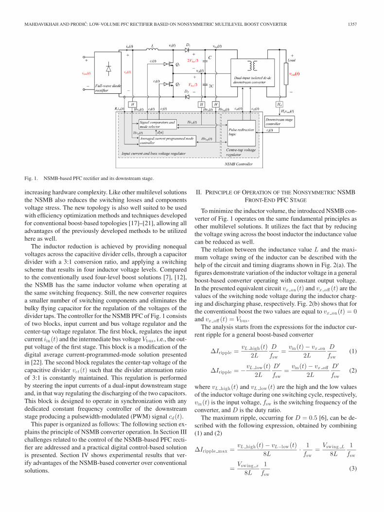
The relation between the inductance value L and the maxi-mum voltage swing of the inductor can be described with thehelp of the circuit and timing diagrams shown in Fig. 2(a). Thefigures demonstrate variation of the inductor voltage in a generalboost-based converter operating with constant output voltage.In the presented equivalent circuit vx on(t) and vx off (t) are thevalues of the switching node voltage during the inductor charg-ing and discharging phase, respectively. Fig. 2(b) shows that forthe conventional boost the two values are equal to vx on(t) = 0and vx off (t) = Vbus .
The analysis starts from the expressions for the inductor cur-rent ripple for a general boost-based converter
ΔIripple =vL high(t)
2L
D
fsw=
vin(t) − vx on
2L
D
fsw(1)
ΔIripple = −vL low (t)2L
D′
fsw=
vin(t) − vx off
2L
D′
fsw(2)
where vL high(t) and vL low (t) are the high and the low valuesof the inductor voltage during one switching cycle, respectively,vin(t) is the input voltage, fsw is the switching frequency of theconverter, and D is the duty ratio.
The maximum ripple, occurring for D = 0.5 [6], can be de-scribed with the following expression, obtained by combining(1) and (2)
ΔIripple max =vL high(t) − vL−low (t)
8L· 1fsw
=Vswing L
8L
1fsw
=Vswing x
8L
1fsw
(3)
1358 IEEE TRANSACTIONS ON POWER ELECTRONICS, VOL. 30, NO. 3, MARCH 2015
Fig. 2. Equivalent circuit for the analysis of the inductor voltage swing and the voltage waveforms of (a) a general boost-based converter and (b) the conventionalboost.
where Vswing L and Vswing x are the voltage swings of the in-ductor and switching node, respectively. It can be seen that theripple, which determines the inductance value [23], is linearlyproportional to the voltage swing across the switching node.The relation also shows that, for the boost-based converters, theinductor voltage swing is equal to the switching node swing andby minimizing that value, the inductor can be reduced withoutaffecting the current ripple amplitude.
This analysis shows that for the conventional boost the switch-ing node voltage swing is equal to its output voltage. In typi-cal PFC rectifiers, this voltage, labeled as Vbus in Fig. 2(b), isfairly high, usually around 400 V, causing the inductor valueand the switching losses to be relatively large. In the appli-cations of interest, the switching losses usually have a largeinfluence on the overall power processing efficiency of the con-verter [5], [6], [24]. The losses also indirectly increase the over-all system volume, by imposing additional cooling requirementsfor the semiconductor components.
To minimize the swing and, therefore, reduce both the induc-tor value and switching losses, in the NSMB converter of Fig. 1,an active capacitive divider with 3:1 conversion ratio replacesthe output capacitor and switches of the conventional boost.This allows the switching node voltage to be changed betweenfour possible values: 0, Vbus/3, 2Vbus/3, and Vbus , effectivelycreating a four-level structure using a three-level configuration.The divider and its switching sequence are designed to allowvx on(t) and vx off (t) to be dynamically changed as the inputvoltage changes, such that the inductor voltage swing is limitedto Vbus/3. This value is three times lower than that of a con-ventional boost and 33% smaller than the voltage swing of thethree-level topologies [6], [7] operating at the same effectiveswitching frequency. As a result, equal reductions of the induc-tor are allowed and large efficiency improvements obtained. Itshould be noted that similar to the solution presented in [6], itwould be possible to operate the NSMB at the twice switchingfrequency of the conventional boost while maintaining the samepower processing efficiency. Such an operation would resultin a six times smaller inductor volume compared to that of theconventional boost but would significantly increase power dissi-pation per unit volume potentially resulting in increased cooling
requirements and reliability problems. For that reason, through-out the paper comparison was performed with the assumptionthat the topologies operate at the same effective switching fre-quency and simultaneous improvements in power processingefficiency and volume reduction are targeted.
A. Nonsymmetric Active Capacitive Divider
The operation of the nonsymmetric capacitive divider canbe explained by looking at the rectified line input voltage anddiagrams of Figs. 3–5. The diagrams describe three distinctivemodes of converter operation, which depend on the instanta-neous value of the rectified line voltage vin(t) = |vline(t)| (seeFig. 1).
Mode 1: For vin(t) < Vbus/3, the converter operates in mode1, depicted with the diagrams of Fig. 3. Throughout this mode,switch SW1 is kept on, reverse biasing the diode D1 , and theother two switches (SW2 and D2) are active, operating at theswitching rate fsw = 1/Tsw . The on time of SW2 , i.e., duty ratio,is regulated by the controller of Fig. 1. The current conductingpaths for the both portions of a switching period are shown inFig. 3 with bold lines, in red, where Fig. 3(a) corresponds to theinductor charging process, i.e., on time of SW2 , and Fig. 3(b)shows its discharging.
It can be seen that during the on-state of SW2 , vx(t) = 0 andduring its off state vx(t) = Vbus/3. Therefore, the maximumvoltage swing across the inductor is Vbus/3 equal to the voltageof the divider bottom capacitor. It should be noted in this modeboth SW2 and D2 operate at Vbus/3 and the switching lossesare lower than those of the conventional boost and three-levelboost, which switches operate at Vbus and Vbus/2, respectively.
This mode is maintained as long as vin (t) is lower than Vbus/3and the condition for the regular boost operation, i.e., the bottomcapacitor voltage is larger than the input voltage, satisfied.
Mode 2: Mode 2 of operation, shown in Fig. 4, occurs forVbus/3 < vin(t) < 2Vbus/3. In this mode, during the first por-tion of a switching period, corresponding to the transistor on-state in the conventional topology, SW1 and D2 are turned onand the switching node voltage is Vbus/3 as it can be seen fromFig. 4(a). During the remaining portion of the switching period,

MAHDAVIKHAH AND PRODIC: LOW-VOLUME PFC RECTIFIER BASED ON NONSYMMETRIC MULTILEVEL BOOST CONVERTER 1359
Fig. 3. Mode 1 of operation of the NSMB front-end stage: (a) input voltage range for mode 1; (b) equivalent circuit of the converter during inductor chargingphase; (c) equivalent circuit during the discharging.
Fig. 4. Mode 2 of operation of the NSMB front-end stage: (a) input voltage range for mode 2; (b) equivalent circuit of the converter during inductor chargingphase; and (c) equivalent circuit during the discharging.
Fig. 5. Mode 3 of operation of the NSMB front-end stage: (a) input voltage range for mode 3; (b) equivalent circuit of the converter during inductor chargingphase; and (c) equivalent circuit during the discharging.
SW2 and D1 are conducting and, as shown in Fig. 4(b), theswitching node voltage is 2Vbus/3. It can be seen that, in thisway, the absolute value of the voltage swing is again limited toVbus/3.
In this mode, the switching losses are approximately the sameas those of the conventional boost (and three-level boost), sincethe total blocking voltage of the two switches operating in theeach portion of a switching interval is equal to that of the con-ventional boost.
Mode 3: Mode 3, shown in Fig. 5, is activated when vin(t)exceeds 2Vbus/3. Throughout this mode, the transistor SW1 isturned off, allowing diode D1 to conduct. In this mode, duringthe first portion of the switching interval, SW2 is conducting andthe voltage across the switching node is 2Vbus/3 as shown inFig. 5(a). During the second portion of the interval, D2 conductsand the switching node voltage is Vbus . Again, the inductorvoltage swing is limited to Vbus/3.
In this mode the switching losses are again lower than that ofthe conventional boost and of the three-level boost, since bothSW2 and the D2 interrupt only one-third of the converter outputvoltage.
Since, as mentioned earlier, in the applications of interest theswitching losses are dominant, an analysis of conduction lossesfor the NSMB is given in Appendix A. It is shown that the
conduction losses depend on the input voltage amplitude andthe amounts of time NSMB spends in each of the three modes.The analysis also shows that, for an optimally designed NSMB,with switches D1 , SW1 rated at 2Vbus/3 and SW2 ,D2 rated atVbus/3, the conduction losses are approximately the same asthose of the conventional boost.
1) Volume Reductiona) Inductor Volume: As shown in the theoretical analysis of
Section II, the NSMB converter reduces the inductor value bythree times compared to the conventional boost while retainingthe same peak inductor current.
Since the inductor volume is proportional to its energy storagecapacity [25], [26]
WE L =12LI2
peak (4)
where Ipeak is the peak inductor, it can be concluded that theinductor volume of the NSMB is three times smaller as well.
It should be noted that compared to the practical two-phaseboost-interleaved PFC solutions [13], [25], [26], the inductorof the NSMB is about two times smaller. Even though theinductance value of the interleaved boost is reduced by fourtimes, compared to the conventional boost the volume reduc-tion is much smaller. As described in [25] and [26], the actually

1360 IEEE TRANSACTIONS ON POWER ELECTRONICS, VOL. 30, NO. 3, MARCH 2015
achievable volume reduction is around a 32%, due to the higherinductor current ripple and, therefore, a larger peak current.
b) Output Capacitor Volume: In the NSMB converter, theoutput capacitor of the conventional boost with a value ofCout , rated at Vout , is replaced with Cout1 = 3Cout/2, ratedat 2Vout/3 and Cout2 = 3Cout , rated at Vout/3. The output ca-pacitance of the boost PFC is chosen to meet desired hold-uptime energy requirement [27] and the output voltage ripple.
By using the same energy-based criteria to compare the ca-pacitors sizes it can be seen that the NSMB has the same totalcapacitor volume as the conventional boost and the three-levelboost, since, ideally, the size of a capacitor is proportional to itsenergy storing capacity [28], i.e., to its 1/2CV 2 product.
The output voltage ripple comprises two components, thehigh-frequency ripple, at the switching frequency, and the low-frequency component at twice the line frequency. In both theconventional boost PFC and the introduced NSMB, the high-frequency component is much smaller than the component atthe twice line frequency and, therefore, can be neglected in theanalysis [23]. The following analysis shows that the dominantlow-frequency component is the same for the both topologies.
To find the amplitude of the dominant ripple, we can look atthe general case, where an increase of the energy ΔE createsa voltage difference ΔV across the capacitor C having an ini-tial voltage V . This voltage difference can be found using thefollowing relation:
ΔE =12C(V + ΔV )2 − 1
2C(V )2 =
12C(2V ΔV + ΔV 2).
(5)For the case when V > ΔV , which is valid for the systems
under investigation, the following approximate expression forthe voltage deviation:
ΔV ≈ ΔE
CV(6)
can be easily derived from (5).For a general PFC, the increase of the energy can be calculated
by looking at the instantaneous power delivered from the acsource [23]
pin(t) = Pload [1 − cos(2ωlinet)] (7)
which, as shown in Fig. 6, has two components, a dc componentequal to the load power Pload and an ac component at twicethe line frequency. The ac portion of this input power (Pin ac(t)shown in Fig. 6(b) creates the dominant output voltage ripple.To calculate the peak-to-peak value of this ripple, the amountof energy stored in the capacitor over a Tline/4 period (shadedarea in the diagram of Fig. 6(b) can be calculated as
ΔEin ac =∫ t0 +T l in e /4
t0
pin ac(t) dt
=∫ t0 +T l in e /4
t0
Pload [− cos(2ωlinet)]dt =Pload
ωline(8)
Fig. 6. Waveforms of the output capacitor voltage of an ideal PFC circuit;(a) instantaneous input power, voltage, and current waveforms; (b) decomposi-tion of input power components; and (c) output capacitor voltage ripple.
and the output capacitor ripple for a boost PFC found by com-bining (6) and (8)
2ΔVout boost =ΔEin ac
CoutVout=
Pload
ωlineCoutVout. (9)
In the case of the NSMB converter, the energy describedwith (8) is stored across the two output capacitors Ctop andCbottom . The distribution of this energy between capacitors, ingeneral, is not equal and depends on the input voltage level andthe portion of the time the converter is spending in each of theoperating modes. However, the total energy given to the systemis the same as in the boost case and can be described with thefollowing expression:
ΔEin ac = ΔEin ac top + ΔEin ac bottom (10)
where ΔEin ac top and ΔEin ac top are the portions of energystored in the top and bottom capacitors, respectively.
By replacing the values in (6) for the NSMB case, the voltageripples for the top and bottom capacitors ΔVtop and ΔVbottom ,respectively, can be obtained as
2ΔVout bottom =ΔEin ac bottom
Cout bottomVout bottom
=ΔEin ac bottom
(3Cout)(Vout/3)=
ΔEin ac bottom
CoutVout(11)
2ΔVout top =ΔEin ac top
Cout topVout top
=ΔEin ac top
(3/2Cout)(2Vout/3)=
ΔEin ac top
CoutVout(12)
and, since both of the ripple voltages are in phase, the overallripple of the NSMB can be found as
2ΔVout NSMB = 2ΔVout top + 2ΔVout bottom
2ΔVout NSMB =ΔEin ac top + ΔEin ac bottom
CoutVout=
ΔEin ac
CoutVout
=Pload
ωlineCoutVout. (13)
MAHDAVIKHAH AND PRODIC: LOW-VOLUME PFC RECTIFIER BASED ON NONSYMMETRIC MULTILEVEL BOOST CONVERTER 1361
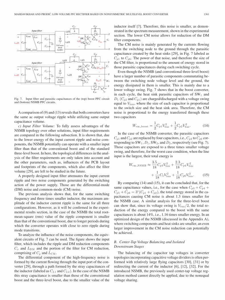
Fig. 7. Input filter and parasitic capacitances of the (top) boost PFC circuitand (bottom) NSMB PFC circuits.
A comparison of (9) and (13) reveals that both converters havethe same ac output voltage ripple while utilizing same outputcapacitance volume.
c) Input Filter Volume: To fully assess advantages of theNSMB topology over other solutions, input filter requirementsare compared in the following subsection. It is shown that, dueto the lower energy of the input current ripple and noise com-ponents, the NSMB potentially can operate with a smaller inputfilter than that of the conventional boost and of the standardthree-level boost. In here, the topological differences in the anal-ysis of the filter requirements are only taken into account andthe other parameters, such as, influences of the PCB layoutand footprints of the components, which also affect the filtervolume [29], are left to be studied in the future.
A properly designed input filter attenuates the input currentripple and two noise components generated by the switchingaction of the power supply. Those are the differential-mode(DM) noise and common-mode (CM) noise.
The previous analysis shows that, for the same switchingfrequency and three times smaller inductor, the maximum am-plitude of the inductor current ripple is the same for all threeconfigurations. However, as it will be confirmed in the experi-mental results section, in the case of the NSMB the total root-mean-square (rms) value of the ripple component is smallerthan that of the conventional boost, due to longer periods duringwhich the converter operates with close to zero ripple duringmode transitions.
To analyze the influence of the noise components, the equiv-alent circuits of Fig. 7 can be used. The figure shows the inputfilter, which includes the ripple and DM reduction componentsCx and LDM and the portion of the filter for CM reduction,comprising of Cy and LCM .
The differential component of the high-frequency noise isformed by the current flowing through the input port of the con-verter [29], through a path formed by the stray capacitances ofthe inductor (labeled as CL1 and CL2). In the case of the NSMBthis stray capacitance is smaller than those of the conventionalboost and the three-level boost, due to the smaller value of the
inductor itself [7]. Therefore, this noise is smaller, as demon-strated in the spectrum measurement, shown in the experimentalsection. The lower CM noise allows for reduction of the DMfilter components.
The CM noise is mainly generated by the currents flowingfrom the switching node to the ground through the parasiticcapacitance created by the heat sinks [29], in Fig. 7 labeled asCp1 to Cp6 . The power of that noise, and therefore the size ofthe CM filter, is proportional to the amount of energy stored inthose parasitic capacitances during each switching cycle.
Even though the NSMB (and conventional three-level boost)have a larger number of parasitic components commutating be-tween the switching node voltage level and the ground, theenergy dissipated in them is smaller. This is mainly due to alower voltage swing. Fig. 7 shows that in the boost converter,in each cycle, the heat sink parasitic capacitors of SW1 andD1 (Cp2 and Cp1) are charged/discharged with a voltage swingequal to Vbus , where the size of each capacitor is proportionalto the switch size and the heat sink area. Therefore, the CMnoise is proportional to the energy transferred through thesetwo capacitors
Wcm boost =12Cp1V
2bus +
12Cp2V
2bus . (14)
In the case of the NSMB converter, the parasitic capacitorsCp1 and Cp2 are replaced by four capacitors, i.e., Cp3 to Cp6 cor-responding to SW1 ,D1 , SW2 , and D2 , respectively (see Fig. 7).Those capacitors are exposed to a three times smaller voltageswing, and therefore, for the worst case condition, when the lineinput is the largest, their total energy is
Wcm NSMB ≈ 3.518
Cp3V2bus +
2.318
Cp4V2bus
+118
C5V2bus +
118
Cp6V2bus . (15)
By comparing (14) and (15), it can be concluded that, for thesame capacitance values, i.e., for the case when Cp3 + Cp4 +Cp5 + Cp6 = 3∗(Cp1 + Cp2), the total energy stored in the ca-pacitances causing CM noise is about 1.3 times smaller forthe NSMB case. A similar analysis for the three-level boostcan show that, since its voltage swing is Vbus/2, the total re-duction of the energy compared to the boost with the samecapacitances is about 14%, i.e., 1.16 times smaller energy. In anoptimized design of the NSMB (discussed in the Appendix A),where switching components and heat sinks are smaller, an evenlarger improvement in the CM noise reduction can potentiallybe achieved.
B. Center-Tap Voltage Balancing and IsolatedDownstream Stages
The balancing of the capacitor tap voltages in convertertopologies incorporating capacitive voltage dividers is often per-formed with relatively large flying capacitors [30], [31] or byredirecting the current of the inductor [6], [12], [32]. For theintroduced NSMB, the previously used center-tap voltage reg-ulation method cannot directly be applied, due to the nonequalvoltage sharing.
1362 IEEE TRANSACTIONS ON POWER ELECTRONICS, VOL. 30, NO. 3, MARCH 2015
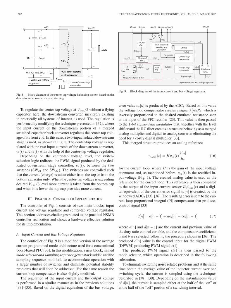
Fig. 8. Block diagram of the center-tap voltage balancing system based on thedownstream converter current steering.
To regulate the center-tap voltage at Vbus/3 without a flyingcapacitor, here, the downstream converter, inevitably existingin practically all systems of interest, is used. The regulation isperformed by modifying the technique presented in [32], wherethe input current of the downstream portion of a mergedswitched-capacitor buck converter regulates the center-tap volt-age of its front end. In this case, a two-input isolated downstreamstage is used, as shown in Fig. 8. The center-tap voltage is reg-ulated with the two input currents of the downstream converter,i1(t) and i2(t) with the help of the center-tap voltage regulator.
Depending on the center-tap voltage level, the switch-selection logic redirects the PWM signal produced by the ded-icated downstream stage controller, cd(t), between the twoswitches (SWd1 and SWd2). The switches are controlled suchthat the current (charge) is taken either from the top or from thebottom capacitor only. When the center-tap voltage is exceedingdesired Vbus/3 level more current is taken from the bottom capand when it is lower the top cap provides more current.
III. PRACTICAL CONTROLLER IMPLEMENTATION
The controller of Fig. 1 consists of two main blocks: inputcurrent and voltage regulator and center-tap voltage regulator.This section addresses challenges related to the practical NSMBcontroller realization and shows a hardware-effective solutionfor its implementation.
A. Input Current and Bus Voltage Regulator
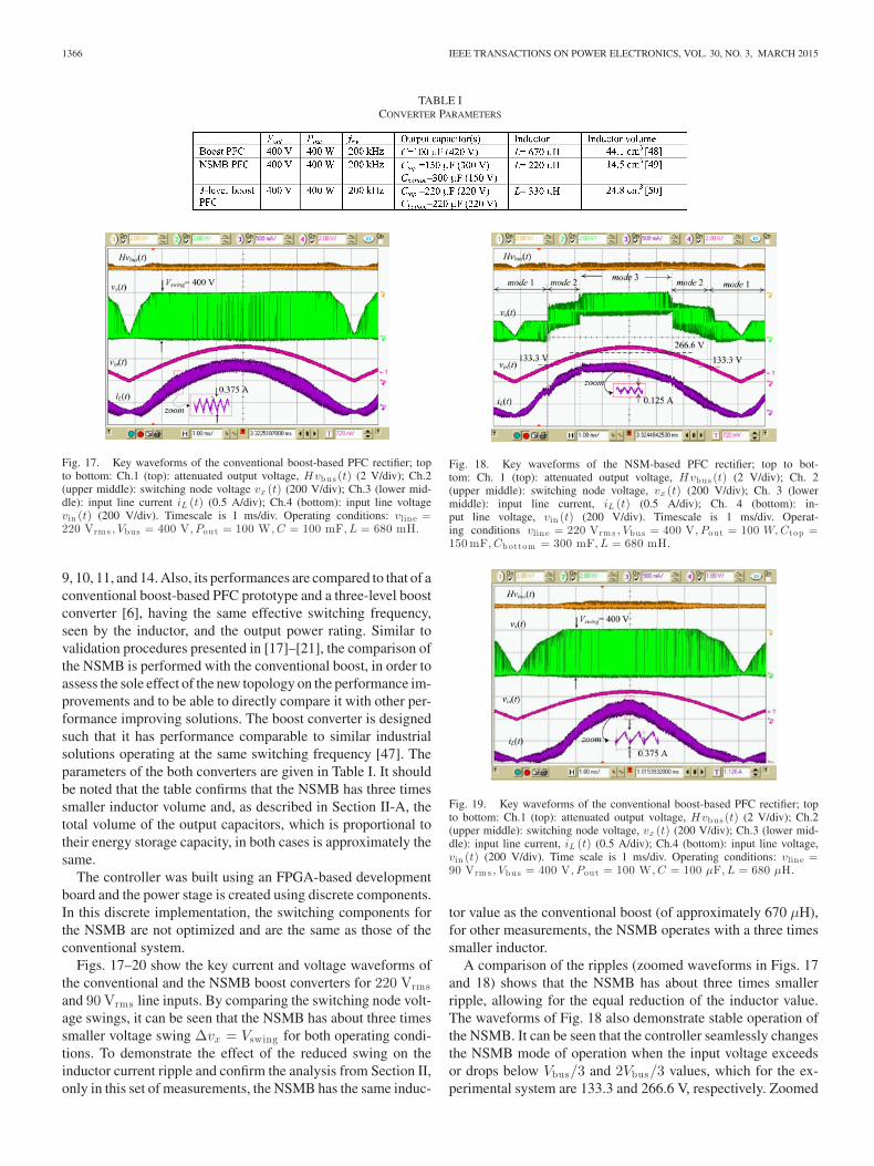
The controller of Fig. 9 is a modified version of the averagecurrent programmed mode architecture used for a conventionalboost-based PFC [33]. In this modification, a new block, namedmode selector and sampling sequence generator is added and thesampling sequence modified, to accommodate operation witha larger number of switches and eliminate potential stabilityproblems that will soon be addressed. For the same reason thecurrent loop compensator is also slightly modified.
The regulation of the input current and the output voltageis performed in a similar manner as in the previous solutions[33]–[35]. Based on the digital equivalent of the bus voltage,
Fig. 9. Block diagram of the input current and bus voltage regulator.
error value ev [n] is produced by the ADC1 . Based on this valuethe voltage loop compensator creates a signal k[n]/Re, which isinversely proportional to the desired emulated resistance seenat the input of the PFC rectifier [23]. This value is then passedto the 1-bit sigma-delta modulator that, together with the levelshifter and the RC filter creates a structure behaving as a mergedanalog multiplier and digital-to-analog converter eliminating theneed for a costly digital multiplier [33].
This merged structure produces an analog reference
vi ref (t) = Hvin(t)k[n]Re
(16)
for the current loop, where H is the gain of the input voltageattenuator and, as mentioned before, vin(t) is the rectified in-put voltage (Fig. 1). The created analog value is used as thereference for the current loop. This reference is then comparedto the output of the input current sensor Rsiline(t) and a digi-tal equivalent of the current error signal ei [n] is created, by thewindowed ADC2 [33], [36]. The resulting error is sent to the cur-rent loop proportional-integral (PI) compensator that producescontrol signal [33]
d[n] = d[n − 1] + aei [n] + bei [n − 1] (17)
where d[n] and d[n – 1] are the current and previous value ofthe duty ratio control variable, and the compensator coefficientsa and b are selected following the procedure shown in [36]. Theproduced d[n] value is the control input for the digital PWM(DPWM) producing PWM signal c(t).
The produced PWM signal c(t) is then passed to themode selector, which operation is described in the followingsubsection.
To eliminate switching noise related problems and at the sametime obtain the average value of the inductor current over oneswitching cycle, the current is sampled using the techniquesdescribed in [38], [39]. Depending on the instantaneous valueof d[n], the current is sampled either at the half of the “on” orat the half of the “off” portion of a switching interval.

MAHDAVIKHAH AND PRODIC: LOW-VOLUME PFC RECTIFIER BASED ON NONSYMMETRIC MULTILEVEL BOOST CONVERTER 1363
Fig. 10. Block diagram of the mode selector and sampling sequence generator.
Fig. 11. State flow diagram of the mode selector logic.
B. Mode Selector and Sampling Sequence Generator
The mode selector and sampling sequence generator, whoseblock diagram is shown in Fig. 10, outputs PWM signals c1(t)and c2(t) for controlling the NSMB transistors SW1 and SW2 ,respectively. During mode transients the selector also changesstored values of the digital current loop compensator, to pro-vide seamless transition between different modes. The de-tection of the mode of operation is performed with the twocomparators (cmp1 and cmp2) and with the start-up logic,shown in Fig. 10. The comparators cmp1 and cmp2 monitorthe input voltage and detect the transition points at which thevin(t) = vct(t) = Vbus/3 and vin(t) = vtop(t) = 2Vbus/3. Thecompensators also initiate mode transition by sending the sig-nals to the mode transition logic. Based on the state of thecomparators and the previous state of the NSMB power stage,the transition logic redirects c(t) to appropriate transistors. Thestart-up detector indicates power up condition of the converterby observing ev [n] and sends the start signal to the mode transi-tion logic, which provides a gradual rise of the bus voltage upona power up. The mode transition logic is a finite-state machine(FSM), which operation is demonstrated with the diagram ofFig. 11 and described in the following sections.
1) Seamless Mode Transitions: To understand the stabilityproblem and a solution for it we can observe how the requiredconversion ratio changes in the conventional boost-based PFCand in the NSMB-based system. In the conventional boost, to
Fig. 12. Waveforms of the sampling sequence generator.
maintain a constant bus voltage, the conversion ratio changesgradually with changes in the input voltage. On the other side,in the NSMB the conversation ratio drastically changes witheach mode transition. Therefore, the duty ratio value requiredfor maintaining the inductor volt–second balance and the stableoutput voltage abruptly changes as well. From a practical pointof view this represents a potential problem, since the delaysin the controller reaction could cause mode transition relatedstability problems.
For example, it can be seen that at the point where the vin(t)is exceeding Vbus/3 (mode 1 to mode 2 transition), the requiredconversion ratio changes from one to infinity, requiring con-troller to change from 0 to the full duty ratio value in a singleswitching cycle.
To overcome this problem, after each mode transition, themode selector immediately reprograms the current and the pre-vious values of the duty ratio in the digital current loop compen-sator, i.e., d[n] and d[n – 1] of (16). This is performed throughthe reprogram signal, shown in Fig. 10. The decision about thenew duty ratio values is made based on the recognition that af-ter each mode transition, the new duty ratio will be either zeroor one. Since at those points, the required conversion ratio ofNSMB is either one or infinite. Therefore, after each transitionpoint is detected by the comparators, the mode control logic ei-ther sets both d[n] and d[n – 1] to 0 or to their maximum value.The diagram of Fig. 10 shows the reprogramming values of thePI compensator for all four mode transitions.
2) Sampling Sequence: By looking at the operation of theNSMB (see Figs. 3–5), it can be noticed that for some switchingstates one of the two output capacitors does not share the sameground with the rest of the circuit. While from the output load,which is galvanically isolated from the front end stage, this doesnot represent a problem, this floating ground affects measure-ments of the capacitor tap voltages. To measure the tap voltageswithout the use of relatively costly differential amplifiers, sam-ple and hold circuits (S&H) shown in Fig. 10 are used, andthe sampling of the capacitor tap voltages is done at particulartime instants denoted by signals smp1 and smp2 as shown inthe diagram of Fig. 12. The value of the top capacitor voltageis sampled during the on state of Q2 and for the bottom ca-pacitor the data acquisition is performed during D2 conductiontime. The ADC1 (see Fig. 1) also samples vtop(t) during D2conduction time, to obtain the bus voltage value.

1364 IEEE TRANSACTIONS ON POWER ELECTRONICS, VOL. 30, NO. 3, MARCH 2015
Fig. 13. Problem of utilizing bypass diode in the NSMB topology.
3) Start Up: The bypass diode commonly used to ease start-up and inrush current problems in conventional boost solution[40] cannot be used with the NSMB and similar multilevelsolutions [4]–[6], [9]. As shown in Fig. 13, the bypass diodeDs [40] would short connect the inductor during the first portionof switching period in mode 3 [see Fig. 5(b)], when vin(t) >vtop(t).
To eliminate the start-up problem, the switching sequenceis modified during power up, signaled by the high value ofstart signal produced by the detector (see Fig. 10). During thismode, the NSMB operates as a conventional boost, such thatboth transistors, i.e., Q1 and Q2 of Fig. 1, are turned on duringthe first portion of a switching interval and D1 and D2 areallowed to conduct during the rest of the switching period, asshown in Fig. 11. Such operation delivers equal amounts ofcharge to the both divider capacitors and, ideally, the desired2:1 distribution of the bus voltage. Possible voltage variationsdue to component tolerances are eliminated with the bleedingresistors [41] Rb forming a 3:1 resistive divider. This mode endswhen the capacitors are charged to their reference values andthe start signal becomes low, causing the NSMB to switch tothe regular mode of operation described in Section II and by thediagram of Fig. 11.
To eliminate the inrush current problem [40] a number ofpreviously presented solutions can be used [40], [42]–[44].
C. Center-Tap Voltage Regulator
As described in the previous section, the regulation of thecapacitor voltages is performed with the input current of thedownstream converter. This process is controlled by the center-tap voltage regulator that redirects current of the downstreamconverter and in that way, regulates the discharging of the bothNSMB capacitors.
The downstream converters that can be used with NSMB havetwo inputs and also utilize the advantages of reduced voltageswing to minimize the volume and switching losses. Two ofmany possible implementations of the downstream stages in-clude two input nonsymmetric flyback [22] and the two-inputnonsymmetric forward. Figs. 14 and 15, describe the operationof the center-tap voltage regulator with a nonsymmetric for-ward converter. The transformer of the forward has two primarywindings, where the winding connected to the top capacitor (i.e.,capacitor with higher voltage) has twice as many turns as theone connected to the bottom capacitor. The current of the topwinding is controlled by the transistor Qd1 and of the bottom
by Qd2 .The output voltage of the downstream stage is regulatedwith its own controller that produces PWM signal cd(t), whichis passed to the center-tap regulator though an optocoupler. Thecenter-tap regulator sends cd(t) either to Qd1 or to Qd2 , creat-ing signals cd1(t) and cd2(t) respectively, as shown in Fig. 15.The two signals are sequenced such that the center-tap voltageis kept at Vbus/3 level. To achieve this, the center-tap voltageis compared with three times attenuated bus voltage using twocomparators (see Fig. 14) whose outputs are connected to theblock named switch selection logic. The switch selection logic(see Fig. 14) implements the charge-balancing algorithm pre-sented in [32], to keep the capacitors voltages regulated.
When the center-tap voltage is inside regulation bandVbus/3 ± Δvct , where Δvct is the allowable center-tap volt-age variation, the switch selection logic alternates the signalcd(t) between Qd1 and Qd2 after each switching cycle of thedownstream converter. As a result, equal voltage drops acrossboth capacitors occur as shown in Fig. 15, since a two timeslarger charge (i.e., current) is taken from the bottom capacitorhaving twice the capacitance value.
If the center-tap voltage exceeds the regulation band, com-parator cmp1 is activated and the regulation sequence is mod-ified, such that the discharging of the top capacitor is skippedfor several cycles, until the center-tap voltage is reduced toVbus/3 level. Similarly, if the center-tap voltage drops belowVbus/3 − Δvct , the comparator cmp2 is triggered and the dis-charging of the bottom capacitor is interrupted for several cycles.
D. Design Tradeoffs
By comparing the practical implementation of the NSMBto that of the conventional boost solution [23], it can be seenthat a design tradeoff is involved. The NSMB requires a largernumber of components (the same as three-level solutions), high-side gate drivers, more complex control, and a nonconventionaldownstream stage. The following section showing experimentalresults demonstrates that in terms of the total volume and powerprocessing efficiency this design is favorable in the targetedapplications, providing 100–500 W of power and operating atswitching frequencies in the range of 100–200 kHz. The induc-tive components and heat sinks are by far the largest contributorsto the overall volume and the weight of the converter. The ex-perimental validation shows that the NSMB has significantlybetter power processing efficiency and lower volume than thesingle-phase and interleaved boost-based solutions, which arepredominantly used in the applications of interest.
Also, the capacitive divider at the output of the NSMB allowsfor a reduction in the volume of the downstream stage andpotentially, its efficiency improvement.
Therefore, it can be envisioned that the advantages of theNSMB can potentially be fully utilized in a system where mul-tiple semiconductor components would be integrated on a semi-conductor chip and optimally sized, in terms of blocking voltageand conducting current. Such an implementation on a dedicatedIC would probably not only result in a reduction of the numberof components but also, as described in the following section,

MAHDAVIKHAH AND PRODIC: LOW-VOLUME PFC RECTIFIER BASED ON NONSYMMETRIC MULTILEVEL BOOST CONVERTER 1365
Fig. 14. Center-tap voltage controller regulating operation of a forward-based downstream stage.
Fig. 15. Key waveforms of the center-tap voltage regulator (from top to bot-tom): cd (t)—PWM signal of the downstream stage controller; cd1 (t)—controlsignal for Qd1 ; cd2 (t)—control signal for Qd2 ; i1 (t)—discharging currentof the top capacitor of the NSMB; i2 (t)—discharging current of the bottomcapacitor of the NSMB.
in further efficiency improvements, due to smaller parasitic ca-pacitances and resistances of the components.
E. Extension to Higher Power Levels
The NSMB configuration of Fig. 1 is primarily designedfor the PFC applications below 500 W. In order to utilize theconverter for higher power ratings, where the conductions lossesare becoming dominant, the concept of interleaving, widely usedwith the conventional solutions [13], [25], could potentially be
Fig. 16. Bridgeless NSMB converter topology.
applied here as well. In this case, multiple single-phase NSMBconverters, each followed by an isolated dc–dc converter couldbe connected in parallel.
For the PFC applications exceeding 1 kW, where, as demon-strated in [17] and [45], the diode rectifier significantly de-grades power processing efficiency, the bridgeless modifica-tion of the NSMB, shown in Fig. 16, could potentially beused. The transformation of the converter into its bridge-less version is performed using the principles demonstratedin [17], [45], and [46]. Validations of potential advantages ofthe modified NSMB topologies over the conventional solutionswould require further investigation and are beyond the scope ofthis paper.
IV. EXPERIMENTAL SYSTEM AND RESULTS
To validate the operation of the introduced nonsymmetricboost-based PFC rectifier, a universal-input 400 W, 200 kHz ex-perimental prototype was built, based on the diagrams of Figs. 1,
1366 IEEE TRANSACTIONS ON POWER ELECTRONICS, VOL. 30, NO. 3, MARCH 2015
TABLE ICONVERTER PARAMETERS
Fig. 17. Key waveforms of the conventional boost-based PFC rectifier; topto bottom: Ch.1 (top): attenuated output voltage, Hvbus (t) (2 V/div); Ch.2(upper middle): switching node voltage vx (t) (200 V/div); Ch.3 (lower mid-dle): input line current iL (t) (0.5 A/div); Ch.4 (bottom): input line voltagevin (t) (200 V/div). Timescale is 1 ms/div. Operating conditions: vline =220 Vrm s , Vbus = 400 V, Pout = 100 W, C = 100 mF, L = 680 mH.
9, 10, 11, and 14. Also, its performances are compared to that of aconventional boost-based PFC prototype and a three-level boostconverter [6], having the same effective switching frequency,seen by the inductor, and the output power rating. Similar tovalidation procedures presented in [17]–[21], the comparison ofthe NSMB is performed with the conventional boost, in order toassess the sole effect of the new topology on the performance im-provements and to be able to directly compare it with other per-formance improving solutions. The boost converter is designedsuch that it has performance comparable to similar industrialsolutions operating at the same switching frequency [47]. Theparameters of the both converters are given in Table I. It shouldbe noted that the table confirms that the NSMB has three timessmaller inductor volume and, as described in Section II-A, thetotal volume of the output capacitors, which is proportional totheir energy storage capacity, in both cases is approximately thesame.
The controller was built using an FPGA-based developmentboard and the power stage is created using discrete components.In this discrete implementation, the switching components forthe NSMB are not optimized and are the same as those of theconventional system.
Figs. 17–20 show the key current and voltage waveforms ofthe conventional and the NSMB boost converters for 220 Vrmsand 90 Vrms line inputs. By comparing the switching node volt-age swings, it can be seen that the NSMB has about three timessmaller voltage swing Δvx = Vswing for both operating condi-tions. To demonstrate the effect of the reduced swing on theinductor current ripple and confirm the analysis from Section II,only in this set of measurements, the NSMB has the same induc-
Fig. 18. Key waveforms of the NSM-based PFC rectifier; top to bot-tom: Ch. 1 (top): attenuated output voltage, Hvbus (t) (2 V/div); Ch. 2(upper middle): switching node voltage, vx (t) (200 V/div); Ch. 3 (lowermiddle): input line current, iL (t) (0.5 A/div); Ch. 4 (bottom): in-put line voltage, vin (t) (200 V/div). Timescale is 1 ms/div. Operat-ing conditions vline = 220 Vrm s , Vbus = 400 V, Pout = 100 W, Ctop =150 mF, Cbottom = 300 mF, L = 680 mH.
Fig. 19. Key waveforms of the conventional boost-based PFC rectifier; topto bottom: Ch.1 (top): attenuated output voltage, Hvbus (t) (2 V/div); Ch.2(upper middle): switching node voltage, vx (t) (200 V/div); Ch.3 (lower mid-dle): input line current, iL (t) (0.5 A/div); Ch.4 (bottom): input line voltage,vin (t) (200 V/div). Time scale is 1 ms/div. Operating conditions: vline =90 Vrm s , Vbus = 400 V, Pout = 100 W, C = 100 μF, L = 680 μH.
tor value as the conventional boost (of approximately 670 μH),for other measurements, the NSMB operates with a three timessmaller inductor.
A comparison of the ripples (zoomed waveforms in Figs. 17and 18) shows that the NSMB has about three times smallerripple, allowing for the equal reduction of the inductor value.The waveforms of Fig. 18 also demonstrate stable operation ofthe NSMB. It can be seen that the controller seamlessly changesthe NSMB mode of operation when the input voltage exceedsor drops below Vbus/3 and 2Vbus/3 values, which for the ex-perimental system are 133.3 and 266.6 V, respectively. Zoomed

MAHDAVIKHAH AND PRODIC: LOW-VOLUME PFC RECTIFIER BASED ON NONSYMMETRIC MULTILEVEL BOOST CONVERTER 1367
Fig. 20. Key waveforms of the conventional boost-based PFC rectifier; topto bottom: Ch. 1 (top): attenuated output voltage, Hvbus (t) (2 V/div); Ch. 2(upper middle): switching node voltage vx (t) (200 V/div); Ch. 3 (lower mid-dle): input line current iL (t) (0.5 A/div); Ch. 4 (bottom): input line volt-age vin (t) (200 V/div). Timescale is 1 ms/div. Operating conditions: vline =90 Vrm s , Vbus = 400 V, Pout = 100 W, C = 100 μF, L = 680 μH.
in transition waveforms are also shown in Fig. 21. These wave-forms demonstrate effectiveness of the applied mode transitionmethod based on the PI compensator re-initialization, describedin Section III. It can be seen that at the transition points, theduty ratio changes from the maximum value to zero (reducingthe swing of inductor voltage to zero as well). By looking atthe waveforms of the both converters a slight current waveformdistortion can be noticed. The distortion occurs due to the quan-tization effects and the loss of the gain of the current measure-ment ADC at low inputs [51]. When the input becomes smallerthan the quantization step of the used 6-bit ADC its gain, andconsequently, the overall gain of the system reduces, causingdistortion of the current waveform. For high-end applications,where a very low harmonic distortion is required, a higher res-olution ADC can minimize this potential drawback.
Fig. 22 illustrates regulation of the output capacitor voltageswith a downstream converter stage with a 70 W output load. Thedownstream stage operates at 200 kHz switching frequency. Itcan be seen that both capacitors maintain stable voltages and thatduring each cycle the charge taken from the bottom capacitoris twice as large as that taken from the top. As described inSection III-D, this results in equal voltage drops across bothcapacitors. It should be noted that, as it can be seen from Fig. 20,at low line inputs, the converter mostly operates in mode 1 (ormodes 1 and 2), causing most of the power to be transferredthrough the bottom portion of the downstream stage of Fig. 14.To handle these conditions, the transistor and the winding onthe bottom primary side of the converter need to be designedsuch that thy can provide the full load power. This drawbackis completely compensated by the fact that the transistor of thedownstream stage operates at a three times smaller voltage thanthat of the conventional downstream solutions [2], [52], [53],where most of the losses at the primary side of the converter arecaused by high voltage stress of the transistors.
Power quality and total harmonic distortion (THD) for bothconverters are also experimentally compared, by extracting thecurrent waveform data from the oscilloscope. In order to captureaccurate information about the inductor currents, the harmonics
Fig. 21. Transitions from mode 1 to mode 2 (top) and from mode 2 to mode 3(bottom); Ch.m1(top): input line voltage, vin (t) (200 V/div); Ch. 2 (upper mid-dle): switching node voltage, vx (t) (200V/div); Ch. 4 (middle): gating signalof SW1 , c1 (t) (20 V/div); Ch. 1 (lower middle): gating signal of SW2 , c2 (t)(20 V/div); Ch. 3 (bottom): input line current, iL (t), (0.5 A/div); digital in-put: mode control signal ((0 = mode 1, 1 = mode 2, 2 = mode 3). Timescaleis 5 μs/div. Operating conditions vline = 220 Vrm s , Vbus = 400 V, Pout =100 W, Ctop = 150 mF, Cbottom = 300 mF, L = 230 mH.
are measured without an input filter regularly existing in theapplications of interest.
In both cases, the power factor is measured to be about 0.98.The harmonic contents for both converters are shown in Fig. 23.It can be seen that the both converters have similar spectrums.The measurements also show that, similar to three-level solu-tions [7], [9], [12], the NSMB has slightly lower THD, i.e.,14.03% versus 15.48%. It should be noted that with the use ofan input filter the THD values should be significantly smaller.The lower THD of the NSMB is mostly due to the lower energyof harmonics at the switching frequency and multiple regions ofoperation with close to zero inductor current ripple, as shown inFig. 21.
Figs. 24 and 25 show efficiency comparison results for aconventional boost, a three-level boost, and NSMB convertersoperating with 85 Vrms and 265 Vrms input voltages, respec-tively. In this case, the boost PFC has power processing ef-ficiency comparable to the commercial solutions operating atthe same switching frequency [47]. The efficiency comparisonexperiments are conducted for all converters operating at thesame 200 kHz effective switching frequency. It can be seen that,mainly due to the reduction of switching losses, the introducedNSMB-PFC has up to 6% better power processing efficiency

1368 IEEE TRANSACTIONS ON POWER ELECTRONICS, VOL. 30, NO. 3, MARCH 2015
Fig. 22. Capacitor taps voltage regulation with the downstream stage cur-rents; top to bottom: Ch.1 (top): top capacitor voltage, vupp er (t) (100 V/div);Ch.2 (upper middle): bottom capacitor voltage, vbottom (t) (100 V/div); Ch.4(lower middle): discharging current of bottom capacitor, i2 (t) ( 1 A/div); Ch.3(bottom): discharging current of top capacitor, i1 (t), (1 A/div);. Time scaleis 2 ms/div. Operating conditions vline = 220 Vrm s , Vbus = 400 V, Pout =70 W, Ctop = 150 mF, Cbottom = 300 mF, L = 230 mH.
Fig. 23. Amplitudes of harmonics (multiples of 50 Hz) around line frequencyand the switching frequency for the NSMB-based PFC prototype (top) and theconventional boost-based prototype (bottom).
than the boost converter and up to 4% than the three-level PFC.The efficiency improvements can be seen throughout the wholeoperating range, where, as expected, at light and medium loads,where the switching losses are dominant, the improvements aremore noticeable.
It should be noted that in all prototypes the same switchingcomponents (Infineon IPB60R280C6CT Cool MOS switches[54] and STTH10LCD06 diodes from STMicroelectronics [55].The maximum voltage rating of all components is 600 V. Thesame components are used due to a limited selection of switch-ing components rated for the required blocking voltage of the
Fig. 24. Efficiency comparison of the conventional boost, three-level boost,and NSMB PFC converters for the line input of 265 Vrm s .
Fig. 25. Efficiency comparison of the conventional boost, three-level boost,and NSMB PFC converters for the line input of 85 Vrm s .
Fig. 26. Loss breakdown analysis for the conventional boost, three-level boost,and NSMB PFC converters for 85 Vrm s and 265 Vrm s input voltages at thelight load operating condition (50 W). Length of each bar is normalized basedon the losses of the boost at 90 Vrm s , which is 9.8 W.
NSMB topology. Therefore, the design has not been optimizedfor the NSMB topology. Still, the obtained efficiency results arecomparable or better than those obtained in the state of the artsolutions operating at the same switching frequency [26].
Figs. 26 and 27 compare the loss breakdown of the boost, thethree-level, and the NSMB converters. The loss analysis results

MAHDAVIKHAH AND PRODIC: LOW-VOLUME PFC RECTIFIER BASED ON NONSYMMETRIC MULTILEVEL BOOST CONVERTER 1369
Fig. 27. Loss breakdown analysis for the conventional boost, three-level boost,and NSMB PFC converters for 85 Vrm s and 265 Vrm s input voltages at thelight load operating condition (350 W for 85 Vrm s and 400 W for 265 Vrm s ).Length of each bar is normalized based on the losses of the boost at 90 Vrm s ,which are 50.5 W.
are shown for operation with the input voltages of 265 Vrms and85 Vrms for two cases for light (Fig. 26) and heavy (Fig. 27)loads of each converter. Each bar in these figures shows the nor-malized losses from different contributors to the overall losses ofthe corresponding converter and operating conditions. The nor-malization is preformed under assumption that the total lossesof the conventional boost have a value of 1.
It is also worth mentioning that most efficiency optimiza-tion techniques and volume reduction methods developed forthe conventional boost-based PFC topologies can be applied tothe NSMB as well. Those include utilization of super junctionand SiC devices [18], variable frequency control [19], sepa-rate light load control scheme [20], [21], and utilization of softswitching techniques [17]. For example, a soft-switched NSMBconverter can be implemented employing the ZVT circuit pre-sented in [6]. This means that, in the NSMB, the benefits of allof these complementary methods can be utilized while main-taining advantages of the smaller inductor and lower voltagestress over the conventional solutions.
In the targeted cost-sensitive applications (below 500 W),the use of a bridgeless topology is usually avoided [13], dueto increased price and fairly limited relative improvements inthe power processing efficiency. This can be demonstrated bylooking at the loss breakdown shown in Figs. 26 and 27. It canbe seen that the diode bridge losses of the NSMB converter area very small portion of the overall losses at light loads (5.1%)and increase at heavy loads, to 9.8%. The heavy load resultsindicate that for, higher power applications which are beyondthe scope of this work, the diode rectifier losses become moredominant and that the use of the bridgeless solution, shown inFig. 16, is fully justifiable.
As mentioned earlier, in a potential implementation withcustom-designed silicon components, even larger efficiencygains could be expected. This would mostly be due to the fur-ther reduction of switching losses, caused by increased transis-tor speed and reduced values of parasitic capacitances of thesemiconductor components.
Fig. 28. Normalized volume distributions of conventional boost-based PFCand three other topologies; two-phase interleaved boost-based PFC, three-levelPFC, and the NSMB-based solution. In case of the latter three cases, a vol-ume break down in case of implementation with optimal switches, i.e., lowervoltage/current rated switches in single package, is also shown.
The diagrams of Fig. 28 compare the volume breakdown be-tween different components and total normalized volumes of theconventional boost PFC, a two-phase interleaved boost-basedPFC [26], a three-level PFC [6], and the introduced NSMB-based solution for typical 300–400 W applications [25], [26],[47]. The diagrams also show volume comparisons for potentialoptimized implementations of the interleaved boost and NSMB,where the silicon switches would be sized in accordance withtheir power ratings and implemented in a single package. Asdescribed in Appendix A, such an optimized implementationwould require the same silicon area as the conventional boost. Itshould be noted that in these comparisons the input filter, whosevolume significantly depends on the printed circuit board (PCB)layout is not taken into account. However, as indicated in theanalysis of Section A-I3, the required volume of the NSMBinput filter is smaller than that of the other analyzed solutions.
It can be seen that compared to the conventional boost, theNSMB has about 30% smaller total volume and is about 15%smaller than the interleaved boost, which, as shown in [25], hasabout 32% smaller inductor than the conventional boost. Thevolume comparison results confirm discussions of the favorabletradeoff from the previous sections. Since in the conventionalboost a large portion of the volume is occupied by the inductorand the heat sink, about 65%, and less than a 5% by the semicon-ductors, a tradeoff between the inductor reduction and efficiencyimprovement on one side and an increase in the semiconductorpart numbers on the other side is favorable. In this, the semi-conductor components include the diode bridge, which in theconventional boost takes about 50% of the total silicon area, andthe diode and the transistor, which take the other 50%. The re-sults show that the three times reduction in the inductor volumeand about a 12% in the heat sink volume, which is proportionalto the heat dissipation reduction, are more than compensatingfor about 50% increase in the semiconductor switch volume anda 60% increase in the volume in the controller size. In this case,the size of the controller is estimated by looking at the volumeof analog components and the number of logic gates requiredfor its implementation for all three cases.

1370 IEEE TRANSACTIONS ON POWER ELECTRONICS, VOL. 30, NO. 3, MARCH 2015
V. CONCLUSION
A rectifier with PFC based on a novel NSMB converter and acomplementary digital controller are introduced. In comparisonwith the conventional boost-based solutions, the NSMB hasthree times smaller inductor as well as reduced switching losses.These advantages are achieved by reducing the inductor, i.e.,switching node, voltage swing to 1/3 of the conventional boostlevel. At the same time, the voltage stress across the switchingcomponents is reduced to 1/3 for one diode–transistor pair andto 2/3 for the other pair.
The NSMB is a modified version of the three-level boosttopology. Instead of having the same voltages across the out-put divider capacitors, this modification uses a nonsymmetriccapacitor divider and the capacitor voltages are regulated at 1/3and 2/3 of the full output voltage level. As a result, a four-leveloperation is achieved reducing the inductor by 33% withoutincreasing the number of components required for implementa-tion.
To control the capacitor voltages of the nonsymmetricaldivider without using a bulky flying capacitor, an isolateddownstream converter is used. In regular operation, the down-stream stage takes nonequal amounts of charge from the capaci-tors keeping the capacitors voltage drops equal during discharg-ing phases. The downstream converter stage has two inputs and,similar to the NSMB, can utilize principles of the reduced volt-age swings to obtain smaller volume of magnetic componentsand reduced switching losses.
The mixed signal controller dynamically changes modes ofthe NSMB operation, depending on the instantaneous input volt-age value. Seamless transitions between three operating modesare provided through the digital PI compensator re-initializationprocess, where, depending on the type of transition, the currentand stored previous values of duty ratio are set to 0 or theirmaximum value. To eliminate the need for differential capacitorvoltage measurements, a switching-state-dependent samplingand hold technique is applied.
Results obtained with an experimental prototype verify thatthe NSMB converter requires a three times smaller inductor andhas significantly better power processing efficiency. The resultsalso demonstrate stable controller operation and seamless modetransitions.
It is important to note that the presented principle of the use ofa nonsymmetric voltage divider to create a four-level converterusing three-level hardware could potentially also be used inthree-level dc–ac converter applications to reduce the volumeof the inductive components.
APPENDIX A
ANALYSIS OF CONDUCTION LOSSES FOR OPTIMIZED
DESIGN OF SWITCHING COMPONENTS
The following analysis and comparison of the conductionlosses are based on the assumption that the semiconductor com-ponents of the both converters are sized in accordance with theirvoltage ratings.
A. Analytical Comparison of Conduction Losses
The conduction losses corresponding to the boost PFC con-verter can approximately be described with the following equa-tion [23]:
Pcond,boost =∫ TL
0[RLboosti
2L (t)
+ Roni2L (t)Dboost(t) + VF iL (t)D′boost(t)]dt
(A1)
where TL is time duration of a half line cycle, iL (t) is the in-ductor current, RLboost is a resistance that models total inductorlosses, Ron is the on resistance of the transistor, VF is the diodeforward voltage drop, and Dboost is the boost converter dutycycle.
For the NSMB converter, due to the change of conduction pathbased on the converter operating mode (as shown in Figs. 3–5),the losses are described with three different equations, corre-sponding to three distinctive modes of work
Pcond,NSMB ,1 =∫
T1
[RLNSMB i2L (t)
+ (Ron,1 + Ron,2)i2L (t)DNSMB ,1(t)
+ (Ron,1i2L (t) + VF 2iL (t))D′
NSMB ,1(t)]dt
(A2)
Pcond,NSMB ,2 =∫
T2
[RLNSMB i2L (t)
+ (Ron,1i2L (t) + VF 2iL (t))DNSMB ,2(t)
+ (Ron,2i2L (t) + VF 1iL (t))D′
NSMB ,2(t)]dt
(A3)
Pcond,NSMB ,3 =∫
T3
[RLNSMB i2L (t)
+ (Ron,2i2L (t) + VF 1iL (t))DNSMB ,3(t)
+ (VF 1iL (t) + VF 2iL (t))D′NSMB ,3(t)]dt
(A4)
where Ti represents the time converter operates in mode i duringa half of line cycle, RLNSMB is equivalent resistance of theNSMB inductor modeling its core and copper losses, Ron is theon resistance of Qi, VF i is forward voltage drop of the diodeDi , and DNSMB ,i corresponds to the duty ratio of the NSMBconverter during mode i.
The total conduction losses can be found as the sum of theprevious three equations
Pcond,NSMB = Pcond,NSMB ,1 +Pcond,NSMB ,2 +Pcond,NSMB ,3 .(A5)
By utilizing volt–second balance [23], the following relationsbetween duty cycles of the boost and the NSMB can be found:
DNSMB ,1(t) = 3Dboost(t) − 2 (A6)
DNSMB ,2(t) = 3Dboost(t) − 1 (A7)

MAHDAVIKHAH AND PRODIC: LOW-VOLUME PFC RECTIFIER BASED ON NONSYMMETRIC MULTILEVEL BOOST CONVERTER 1371
DNSMB ,3(t) = 3Dboost(t). (A8)
Assuming that area used for implementing the transistors ofthe NSMB is the same as that needed for the boost transistor andtaking into account that the on resistance of a power a MOSFETper unit silicon area is given by [56]
Ron sp = α · V 2B (A9)
where α is a process-dependent constant and VB is the break-down voltage, the following relations between the on resistancesof the MOSFET resistances can be found:
Ron,1 =49Ron (A10)
Ron,2 =19Ron (A11)
where Ron is the resistance of the boost transistor and Ron,1and Ron,2 are the resistances of the NSMB. The equations areobtained by taking into account that the blocking voltages ofQ1 and Q2 are a 66% and a 33% of that of the boost transistor,respectively.
By combining (A2)–(A8), (A10)–(A11), and assuming thatthe forward voltage drops of all the diodes are the same, thefollowing relation between the conduction losses of the twotopologies is obtained:
Pcond ,NSM B = Pcond ,boost +∫
T 1
2VF D′boost(t)iL (t)dt
+∫
T 2VF Dboost (t)iL (t)dt +
∫T 3
[VF − 2VF Dboost (t)] iL (t)dt
−∫
T 1
(23Dboost (t) −
29
)Ron i2L (t)dt −
∫T 2
29Ron i2L (t)dt
−∫
T 3
23Dboost (t)Ron i2L (t)dt−
∫ TL
0(RLboost−RLNSM B ) i2L (t)dt.
(A12)
The results show that the diodes losses of the NSMB areslightly higher. The value of the diode losses depends on theinput voltage level, i.e., on the portions of time the NSMB spentin each mode of operation. However, these extra losses can bepartially or completely compensated by the smaller transistorconduction losses and also smaller inductance of the NSMBresulting in lower copper and conduction losses.
REFERENCES
[1] B. Sharifipour, J. S. Huang, P. Liao, L. Huber, and M. M. Jovanovic,“Manufacturing and cost analysis of power-factor-correction circuits,” inProc. IEEE-APEC Annu. Meeting, 1998, vol. 1, pp. 490–494.
[2] O. Garcia, J. A. Cobos, R. Prieto, P. Alou, and J. Uceda, “Power factorcorrection: A survey,” in Proc. IEEE PESC, 2001, pp. 8–13.
[3] Y. Jang and M. M. Jovanovic, “Interleaved boost converter with intrinsicvoltage-doubler characteristic for universal-line PFC front end,” IEEETrans. Power Electron., vol. 22, no. 4, pp. 1394–1401, Jul. 2007.
[4] J. Salmon, A. Knight, J. Ewanchuk, and N. Noor, “Multi-level singlephase boost rectifiers using coupled inductors,” in Proc. IEEE PESC,2008, pp. 3156–3163.
[5] D. Maksimovic and R. Erickson, “Universal-input, high-power-factor,boost doubler rectifiers,” in Proc. IEEE APEC, 1995, vol. 1, pp. 459–465.
[6] M. T. Zhang, Y. Jiang, F. C. Lee, and M. M Jovanovic, “Single-phasethree-level boost power factor correction converter,” in Proc. IEEE APEC,1995, vol. 1, pp. 434–439.
[7] F. Forest, T. A. Meynard, S. Faucher, F. Richardeau, J. J. Huselstein, andC. Joubert, “Using the multilevel imbricated cells topologies in the de-sign of low-power power-factor-corrector converters,” IEEE Trans. Ind.Electron., vol. 52, no. 1, pp. 151–161, Feb. 2005.
[8] D. Damasceno, L. Schuch, and J. R. Pinheiro, “Design procedure to min-imize boost PFC volume concerning the trade-offs among switching fre-quency, input current ripple and soft-switching,” in Proc. IEEE PESC,2005, pp. 2333–2338.
[9] B.-R. Lin and T.-Y. Yang, “Single-phase three-level converter for powerfactor correction,” in Proc. Circuits Syst. ISCAS, 2004, vol. 5, pp. V-960–V-963.
[10] H. Keyhani and H. A. Toliyat, “Flying-capacitor boost converter,” in Proc.IEEE APEC, 2012, pp. 2311–2318.
[11] J. Salmon, A. Knight, J. Ewanchuk, and N. Noor, “Multi-level singlephase boost rectifiers using coupled inductors,” in Proc. IEEE PESC,2008, pp. 3156–3163.
[12] T. A. Meynard and H. Foch, “Multi-level conversion: High voltage chop-pers and voltage-source inverters,” in Proc. IEEE PESC, 1992, vol. 1,pp. 397–403.
[13] L. Balogh and R. Redl, “Power-factor correction with interleaved boostconverters in continuous-inductor-current mode,” in Proc. IEEE APEC,1993, pp. 168–174.
[14] P. W. Lee, Y. S. Lee, D. K. W. Cheng, and X. C. Liu, “Steady-State analy-sis of an interleaved boost converter with coupled inductors,” IEEE Trans.Ind. Electron., vol. 47, no. 4, pp. 787–795, Aug. 2000.
[15] B. A. Miwa, D. M. Otten, and M. E. Schlecht, “High efficiency powerfactor correction using interleaving techniques,” in Proc. IEEE APEC,1992, pp. 557–568.
[16] C. Wang, “Investigation on interleaved boost converters and applications,”Ph.D. dissertation, Virginia Polytech. Inst. State Univ., Blacksburg, VA,USA, Jul. 2009.
[17] Y. Jang, M. M. Jovanovic, K. Fang, and Y. Chang, “High-power-factorsoft-switched boost converter,” IEEE Trans. Power Electron., vol. 21,no. 1, pp. 98–104, Jan. 2006.
[18] F. Chimento, S. Musumeci, A. Raciti, M. Melito, and G. Sorrentino,“Super-Junction MOSFET and SiC diode application for the efficiencyimprovement in a boost PFC converter,” in Proc. IEEE IECON, 2006,pp. 2067–2072.
[19] F. Chen and D. Maksimovic, “Digital control for improved efficiency andreduced harmonic distortion over wide load range in boost PFC rectifiers,”IEEE Trans. Power Electron., vol. 25, no. 10, pp. 2683–2692, Oct. 2010.
[20] H. Kim, J. Kim, K. Park, H. Seong, G. Moon, and M. Youn, “On/Off con-trol of boost PFC converters to improve light-load efficiency in paralleledpower supply units for servers,” IEEE Trans. Ind. Electron., vol. 61, no. 3,pp. 1235–1242, Mar. 2014.
[21] W. Wang and Y. Tzou, “Light load efficiency improvement for AC/DCboost PFC converters by digital multi-mode control method,” in Proc.IEEE PEDS, 2011, pp. 1025–1030.
[22] B. Mahdavikhah, R. Dicecco, and A. Prodic, “Low-volume PFC recti-fier based on non-symmetric multi-level boost converter,” in Proc. IEEEAPEC, 2013, pp. 1030–1034.
[23] R. W. Erickson and D. Maksimovic, Fundamentals of Power Electronics.New York, NY: Springer Media, 2001.
[24] M. M. Jovanovic and J. Yungtaek, “State-of-the-art, single-phase, ac-tive power-factor-correction techniques for high-power applications - anoverview,” IEEE Trans. Ind. Electron., vol. 52, no. 3, pp. 701–708, Jun.2005.
[25] M. O’loughlin, An interleaving PFC pre-regulator for high-power con-verters, presented at Texas Instruments Seminar [Online]. Available:http://www.ti.com/download/trng/docs/seminar/Topic5MO.pdf
[26] “UCC28070 300-W Interleaved PFC Pre-Regulator Design,” Texas In-struments, Dallas, USA, Application Note, Jul. 2010.
[27] Q. Zhao, F. C. Lee, and F. S. Tsai, “Voltage and current stress reduction insingle-stage power factor correction AC/DC converters with bulk capacitorvoltage feedback,” IEEE Trans. Power Electron., vol. 17, no. 4, pp. 477–484, Jul. 2002.
[28] R. Aparicio and A. Hajimiri, “Capacity limits and matching properties oflateral flux integrated capacitors,” in Proc. IEEE Customs Integr. CircuitsConf., May 2001, pp. 365–368.
[29] D. Cochrance, “Passive cancellation of common-mode electromagneticinterference in switching power converters,” M.Sc. thesis, Virginia Poly-tech. Inst. State Univ., Blacksburg, VA, USA, Aug. 2010.

1372 IEEE TRANSACTIONS ON POWER ELECTRONICS, VOL. 30, NO. 3, MARCH 2015
[30] J. Sun, M. Xu, Y. Ying, and F. C. Lee, “High power density, high efficiencysystem two-stage power architecture for laptop computers,” in Proc. IEEEPESC, 2006, pp. 1–7.
[31] R. C. N. Pilawa-Podgurski, D. M. Giuliano, and D. J. Perreault, “Mergedtwo-stage power converter architecture with soft charging switched-capacitor energy transfer,” in Proc. IEEE PESC, 2008, pp. 4008–4015.
[32] A. Radic and A. Prodic, “Buck converter with merged active charge-controlled capacitive attenuation,” IEEE Trans. Power Electron., vol. 27,no. 3, pp. 1049–1054, Mar. 2012.
[33] A. Prodic, “Digital controller for high-frequency rectifiers with powerfactor correction suitable for on-chip implementation,” in Proc. PCC,2007, pp. 1527–1531.
[34] S. Buso, P. Mattavelli, L. Rossetto, and G. Spiazzi, “Simple digital controlimproving dynamic performance of power factor preregulators,” IEEETrans. Power Electron., vol. 18, no. 5, pp. 814–823, Sep. 1998.
[35] A. H. Mitwalli, S. B. Leeb, G. C. Verghese, and V. J. Thottuvelil, “Anadaptive digital controller for a unity power factor converter,” IEEE Trans.Power Electron., vol. 11, no. 2, pp. 374–382, Mar. 1996.
[36] A. Parayandeh and A. Prodic, “Programmable analog-to-digital converterfor low-power DC–DC SMPS,” IEEE Trans. Power Electron., vol. 23,no. 1, pp. 500–505, Jan. 2008.
[37] A. Prodic, D. Maksimovic, and R. W. Erickson, “Design and implementa-tion of a digital PWM controller for a high-frequency switching DC–DCpower converter,” in Proc. IEEE IECON, 2001, vol. 2, pp. 893–898.
[38] D. M. VandeSype, K. DeGusseme, F. M. L. L DeBelie, A. P. Vanden-Bossche, and J. A. Melkebeek, “Small-signal z-domain analysis of digi-tally controlled converters,” IEEE Trans. Power Electron., vol. 21, no. 2,pp. 470–478, Mar. 2006.
[39] Z. Zhenyu, A. Prodic, and P. Mattavelli, “Self-programmable PID com-pensator for digitally controlled SMPS,” in Proc. IEEE COMPEL, 2006,pp. 112–116.
[40] B. T. Lynch, “Under the hood of a DC/DC boost converter,” presentedat the TI Power Supply Design Seminar, Dallas, TX, USA, 2008–2009,Paper SEM1800.
[41] R. B. Standler, Protection of Electronic Circuits from Overvoltages. Mi-neola, USA: Courier Dover Publications, 2002.
[42] M. Allen, “Understanding power supplies and inrush current,” Phelps,USA, Bear Power Supplies, Electron. Products, Jan. 2006.
[43] C. Glaser, “Extending soft start time in TPS6107x family of boost convert-ers,” Texas Instrum., Dallas, USA, Appl. Report SLVA307, Aug. 2008.
[44] A. S. Kislovski, “Fast active inrush current limiter for boost-based resistoremulators,” in Proc. INTELEC, 1994, pp. 649–652.
[45] F. Musavi, W. Eberle, and W. G. Dunford, “A high-performance single-phase bridgeless interleaved PFC converter for plug-in hybrid electricvehicle battery chargers,” IEEE Trans. Ind. Appl., vol. 47, no. 4, pp. 1833–1843, Jul./Aug. 2011.
[46] D. M. Mitchell, “AC–DC converter having an improved power factor,”U.S. Patent 4 412 277, Oct. 25, 1983.
[47] M. Scherf and W. Frank, “200 W SMPS demonstration board II,” InfineonTechnol., Neubiberg, Germany, Application Note AN-CoolMOS 09, 2004.
[48] CTX-10 Series Low-Cost Power Inductors, Cooper Bussmann, Chicago,USA, Datasheet, 2007.
[49] PCV-2 Inductor Series, Coilcraft, cary, USA, Datasheet, 2014.[50] CTX-16–17769 Inductor, Chicago, USA: Cooper Bussmann, Datasheet.
[51] H. Peng, D. Maksimovic, A. Prodic, and E. Alarcon, “Modeling of quan-tization effects in digitally controlled DC–DC converters,” in Proc. IEEEPESC, 2004, vol. 6, pp. 4312–4318.
[52] J. Sebastian, P. Villegas, F. Nuno, and M. M. Hernando, “Very efficienttwo-input DC-to-DC switching post-regulators,” in Proc. IEEE PESC’96,2006, pp. 874–880.
[53] G. Spiazzi, “Analysis of buck converters used as power factor pre-regulators,” in Proc. IEEE PESC, 1997, pp. 564–570.
[54] IPx65R660CFD CoolMOS CFD2 Power Transistor, Infenion Technolo-gies AG, Neubiberg, Germany, Datasheet, 2011.
[55] STTH10LCD06 Ultra Fast Diode, STMicroelectronics, Geneva, Switzer-land, Datasheet, 2010.
[56] B. J. Baliga, Fundamentals of Power Semiconductor Devices. New York,NY, USA: Springer, 2008.
Behzad Mahdavikhah (SM’11) received the B.Sc.degree in electrical engineering from Sharif Univer-sity of Technology, Tehran, Iran, and the M.A.Sc.degree in electrical engineering from McMaster Uni-versity, Hamilton, ON, Canada, in 2007 and 2009,respectively. He is currently working toward thePh.D. degree in electrical engineering, University ofToronto, Canada.
Since September 2009, he has been a Research As-sistant at the Laboratory for Power Management andSwitch-Mode Power Supplies, University of Toronto.
His research interests include converter topologies, digital control techniquesand mixed-signal IC design for high-frequency switch-mode power supplies.
leksandar Prodic (M’03) received the Dipl. Ing. de-gree from the University of Novi Sad, Serbia, in 1994,and the M.Sc. and Ph.D. degrees from the Universityof Colorado in Boulder, Boulder, CO, USA, in 2000and 2003, respectively.
He is a Professor at the ECE Department of theUniversity of Toronto, where, in 2004, he formedLaboratory for Power Management and IntegratedSMPS. His research interests include low to mediumpower converter topologies, mixed-signal control oflow power highfrequency switchmode power sup-
plies (SMPS), and mixedsignal IC design for power electronics. In those areashe has more than 80 journal and conference publications. He also has a numberof inventions that have become commercial products.
Prof Prodic received the IEEE Power Electronics Transactions Paper Awardand several conference paper awards. He also received the 2012 and 2013 Inven-tor of the Year Awards from the University of Toronto. He is especially proudof three Excellence in Teaching Awards, elected and given by the University ofToronto undergraduate students.