04/04/02 EECS 312 1 Lecture 24: Interconnect parasitics EECS 312 Reading: 8.2.1, 8.4.2 (text), 4.2, 4.3.1 (2 nd edition)

04/04/02EECS 3121 Lecture 24: Interconnect parasitics EECS 312 Reading: 8.2.1, 8.4.2 (text), 4.2, 4.3.1 (2 nd edition)
Dec 21, 2015
Welcome message from author
This document is posted to help you gain knowledge. Please leave a comment to let me know what you think about it! Share it to your friends and learn new things together.
Transcript
04/04/02 EECS 312 1
Lecture 24: Interconnect parasitics
EECS 312
Reading: 8.2.1, 8.4.2 (text), 4.2, 4.3.1 (2nd edition)
04/04/02 EECS 312 2
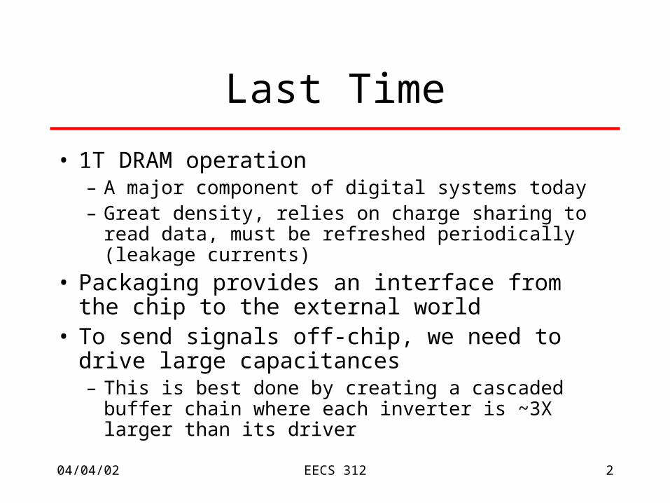
Last Time
• 1T DRAM operation– A major component of digital systems today– Great density, relies on charge sharing to read data,
must be refreshed periodically (leakage currents)
• Packaging provides an interface from the chip to the external world
• To send signals off-chip, we need to drive large capacitances– This is best done by creating a cascaded buffer chain
where each inverter is ~3X larger than its driver
04/04/02 EECS 312 3
Lecture Overview
• Simultaneous switching noise (L*di/dt noise)
• Introduce wiring capacitance
• Models to calculate these parameters
04/04/02 EECS 312 4
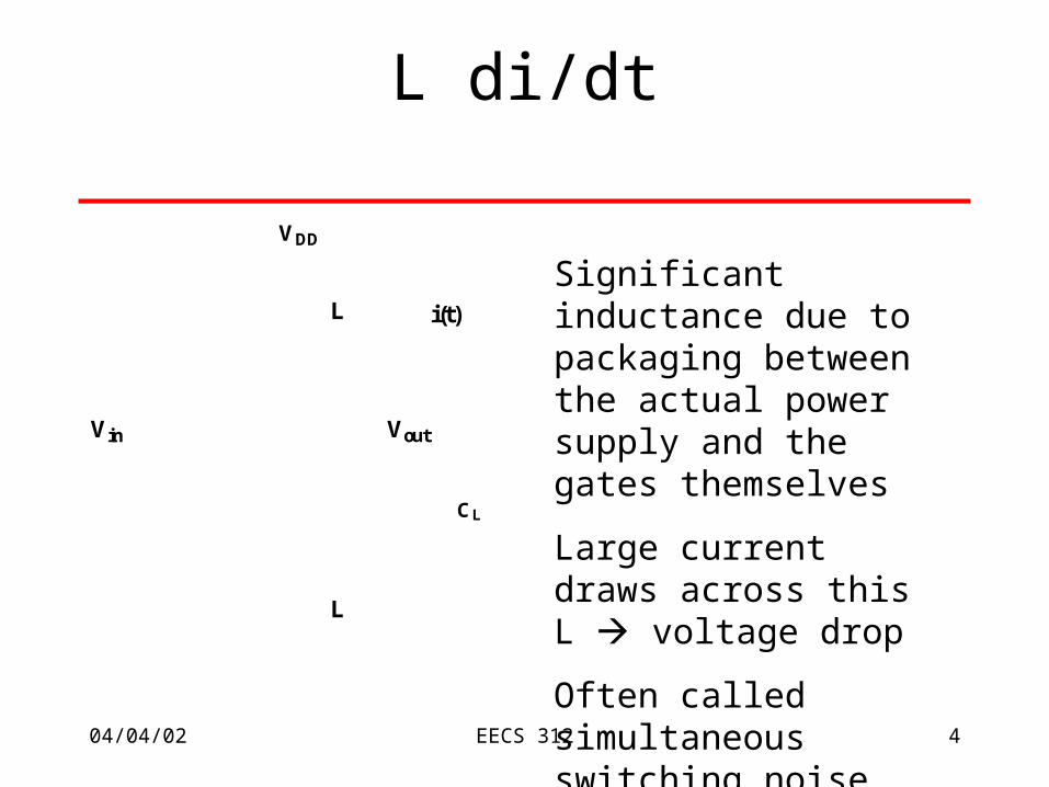
L di/dt
VDD
L
L
VoutVin
CL
i(t)
Significant inductance due to packaging between the actual power supply and the gates themselves
Large current draws across this L voltage drop
Often called simultaneous switching noise (SSN) since a lot of simultaneous switching will increase di/dt
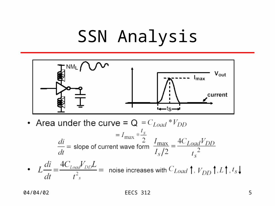
04/04/02 EECS 312 5
SSN Analysis
04/04/02 EECS 312 6
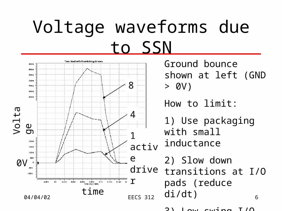
Voltage waveforms due to SSN
8
4
1 active driver
Ground bounce shown at left (GND > 0V)
How to limit:
1) Use packaging with small inductance
2) Slow down transitions at I/O pads (reduce di/dt)
3) Low-swing I/O – incompatible with external chips (usually I/O voltage > regular voltage)
time
Vol
tage
0V
04/04/02 EECS 312 7
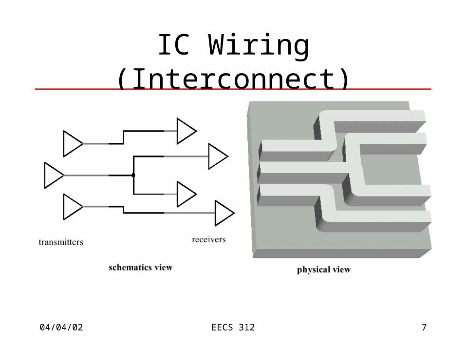
IC Wiring (Interconnect)

04/04/02 EECS 312 8
Impact of Interconnect Parasitics
• Reduce Reliability
• Affect Performance
Classes of Parasitics
• Capacitive
• Resistive
• InductiveNot covered in 312
04/04/02 EECS 312 9
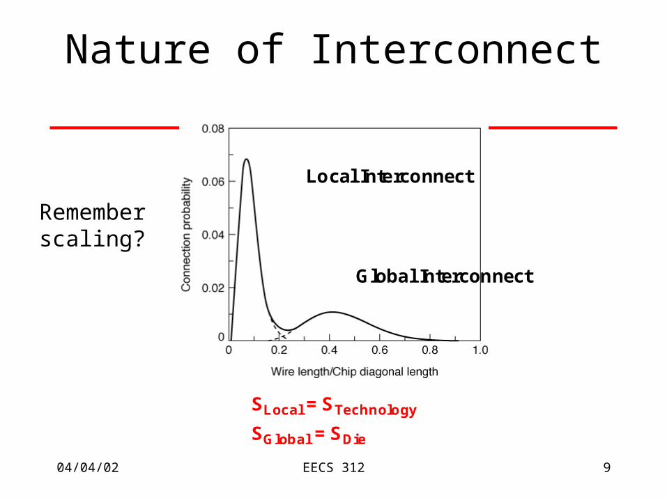
Nature of Interconnect
Local Interconnect
Global Interconnect
SLocal = STechnology
SGlobal = SDie
Remember scaling?
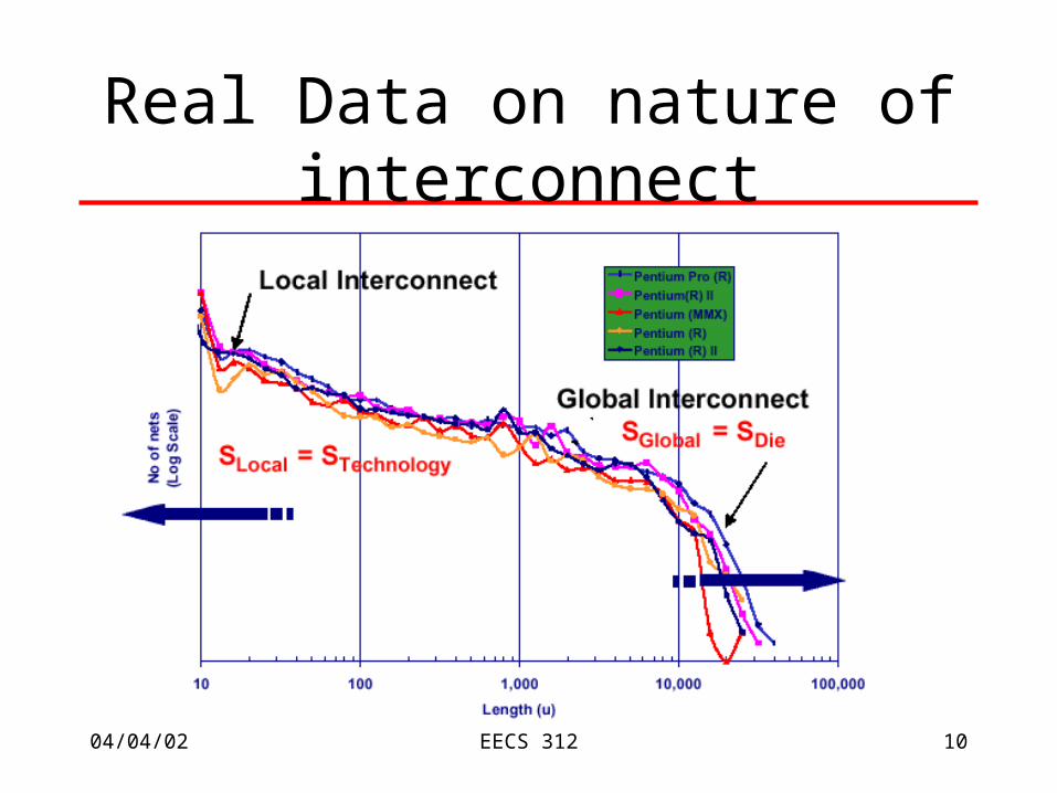
04/04/02 EECS 312 10
Real Data on nature of interconnect
04/04/02 EECS 312 11
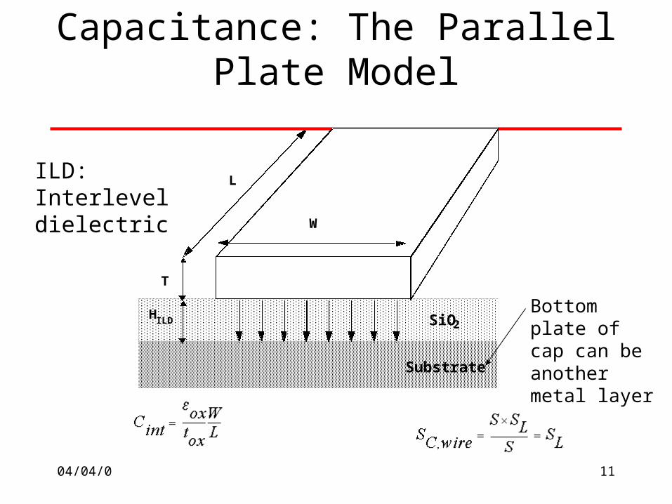
Capacitance: The Parallel Plate Model
SiO2
Substrate
L
W
T
HILD
ILD: Interlevel dielectric
Bottom plate of cap can be another metal layer
04/04/02 EECS 312 12
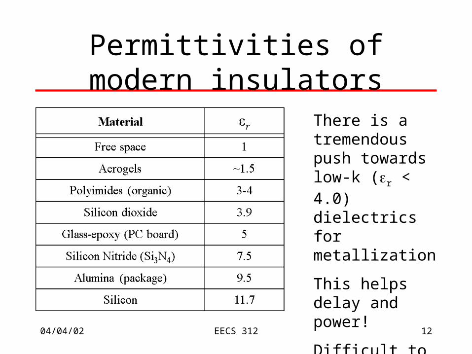
Permittivities of modern insulators
There is a tremendous push towards low-k (r < 4.0) dielectrics for metallization
This helps delay and power!
Difficult to manufacture
04/04/02 EECS 312 13
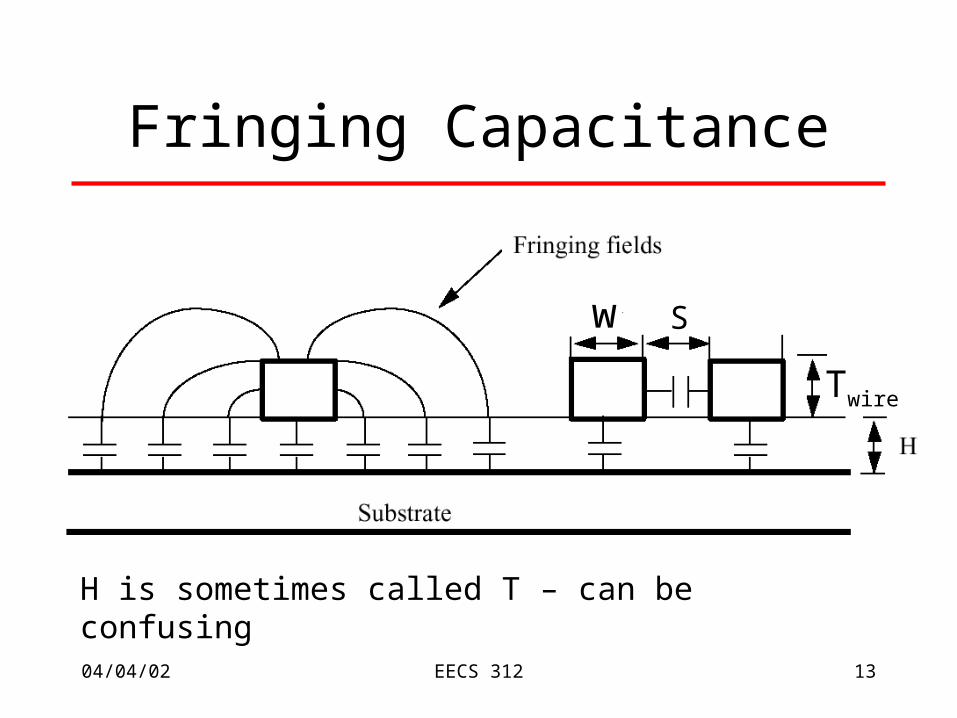
Fringing Capacitance
w S
Twire
H is sometimes called T – can be confusing
04/04/02 EECS 312 14
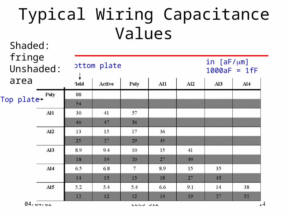
Typical Wiring Capacitance Values
Top plate
Bottom plate in [aF/m]1000aF = 1fF
Shaded: fringeUnshaded: area
04/04/02 EECS 312 15
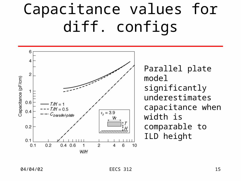
Capacitance values for diff. configs
Parallel plate model significantly underestimates capacitance when width is comparable to ILD height
04/04/02 EECS 312 16
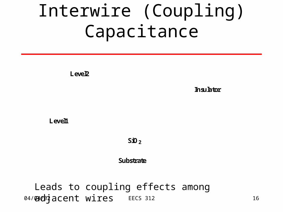
Interwire (Coupling) Capacitance
Substrate
SiO2
Insulator
Level1
Level2
Creates Cross-talkLeads to coupling effects among adjacent wires
04/04/02 EECS 312 17
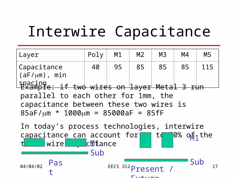
Interwire Capacitance
Layer Poly M1 M2 M3 M4 M5
Capacitance (aF/m), min spacing
40 95 85 85 85 115
Example: if two wires on layer Metal 3 run parallel to each other for 1mm, the capacitance between these two wires is 85aF/m * 1000m = 85000aF = 85fF
In today’s process technologies, interwire capacitance can account for up to 80% of the total wire capacitance
Past
M1Sub
Present / Future
M1
Sub
04/04/02 EECS 312 18
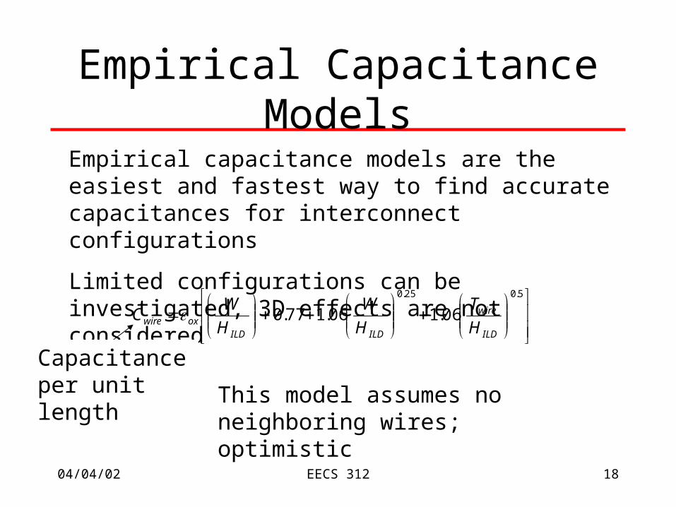
Empirical Capacitance Models
Empirical capacitance models are the easiest and fastest way to find accurate capacitances for interconnect configurations
Limited configurations can be investigated, 3D effects are not considered
5.025.0
06.106.177.0ILD
wire
ILDILDoxwire H
T
H
W
H
WC
Capacitance per unit length This model assumes no neighboring
wires; optimistic
04/04/02 EECS 312 19
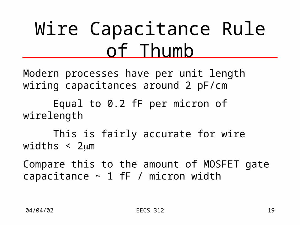
Wire Capacitance Rule of Thumb
Modern processes have per unit length wiring capacitances around 2 pF/cm
Equal to 0.2 fF per micron of wirelength
This is fairly accurate for wire widths < 2m
Compare this to the amount of MOSFET gate capacitance ~ 1 fF / micron width
04/04/02 EECS 312 20
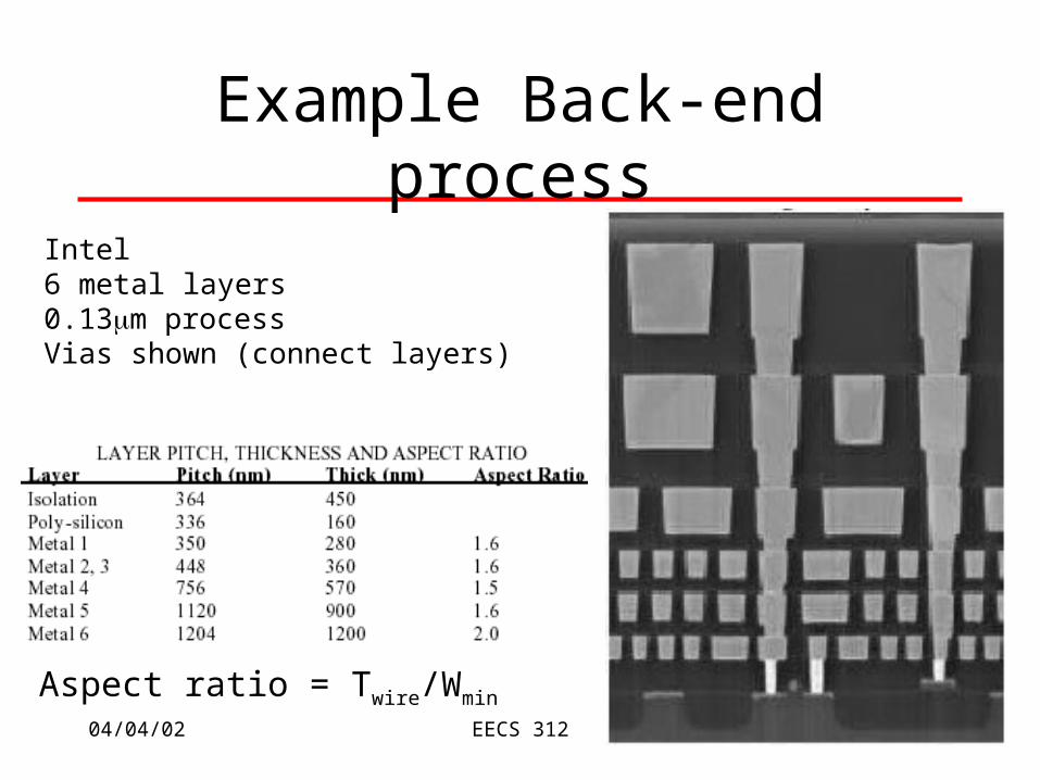
Example Back-end process
Intel6 metal layers0.13m processVias shown (connect layers)
Aspect ratio = Twire/Wmin
04/04/02 EECS 312 21
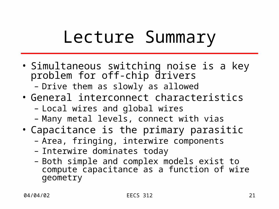
Lecture Summary
• Simultaneous switching noise is a key problem for off-chip drivers– Drive them as slowly as allowed
• General interconnect characteristics– Local wires and global wires– Many metal levels, connect with vias
• Capacitance is the primary parasitic– Area, fringing, interwire components– Interwire dominates today– Both simple and complex models exist to compute
capacitance as a function of wire geometry
04/04/02 EECS 312 22
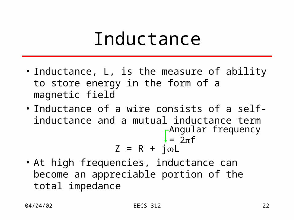
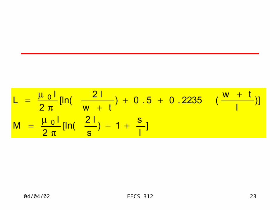
Inductance
• Inductance, L, is the measure of ability to store energy in the form of a magnetic field
• Inductance of a wire consists of a self-inductance and a mutual inductance term
Z = R + jL
• At high frequencies, inductance can become an appreciable portion of the total impedance
Angular frequency = 2f
04/04/02 EECS 312 23
04/04/02 EECS 312 24
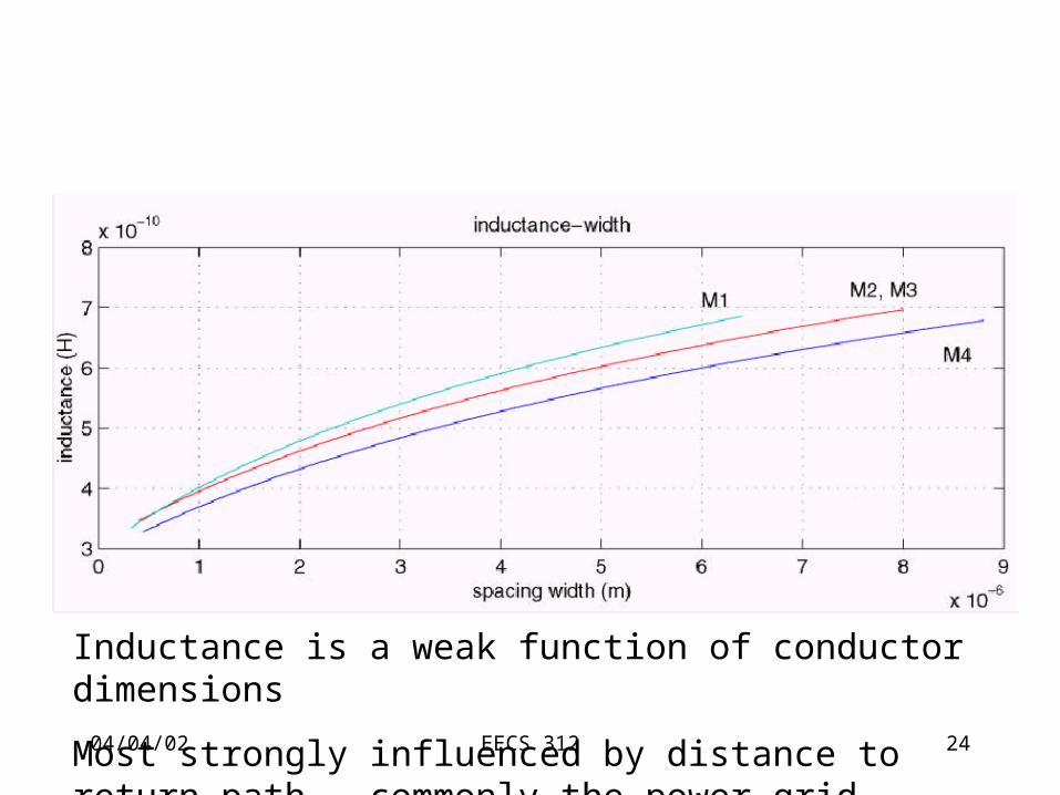
Inductance is a weak function of conductor dimensions
Most strongly influenced by distance to return path – commonly the power grid
04/04/02 EECS 312 25
04/04/02 EECS 312 26
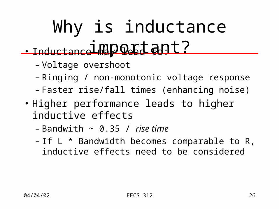
Why is inductance important?• Inductance may lead to:
– Voltage overshoot– Ringing / non-monotonic voltage response– Faster rise/fall times (enhancing noise)
• Higher performance leads to higher inductive effects– Bandwith ~ 0.35 / rise time– If L * Bandwidth becomes comparable to R,
inductive effects need to be considered
04/04/02 EECS 312 27
04/04/02 EECS 312 28
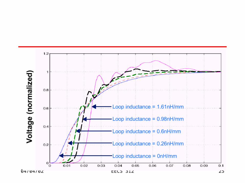
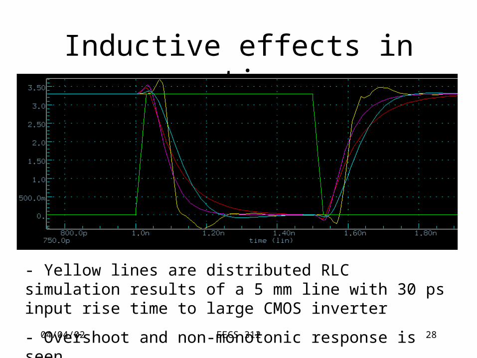
Inductive effects in action
- Yellow lines are distributed RLC simulation results of a 5 mm line with 30 ps input rise time to large CMOS inverter
- Overshoot and non-monotonic response is seen
04/04/02 EECS 312 29
Inductance Trends• Inductance is a weak function of conductor
dimensions (logarithmic)
• Inductance is a strong function of current return path distance– Want to have a nearby ground line to provide a
small current loop
• Inductance is most significant in long, fast-switching nets with low resistance– Clocks are the most susceptible
04/04/02 EECS 312 30
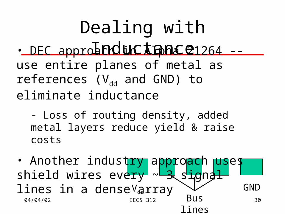
Dealing with Inductance
Bus linesVdd
GND
• DEC approach in Alpha 21264 -- use entire planes of metal as references (Vdd and GND) to eliminate inductance
- Loss of routing density, added metal layers reduce yield & raise costs
• Another industry approach uses shield wires every ~ 3 signal lines in a dense array
04/04/02 EECS 312 31
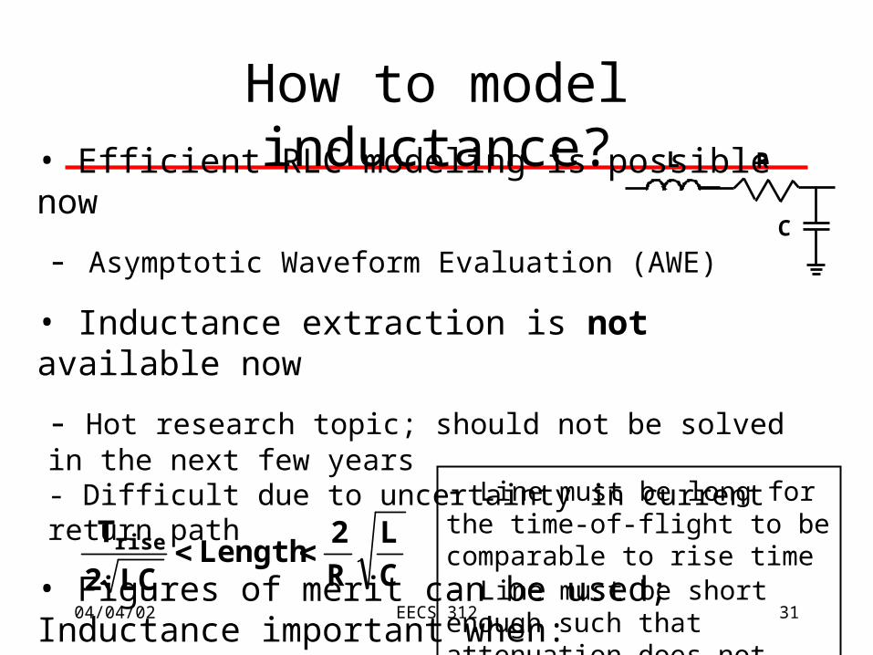
How to model inductance?• Efficient RLC modeling is possible now
- Asymptotic Waveform Evaluation (AWE)
• Inductance extraction is not available now
- Hot research topic; should not be solved in the next few years- Difficult due to uncertainty in current return path
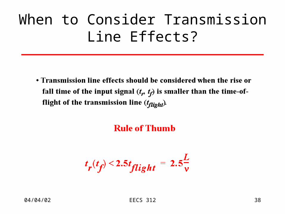
• Figures of merit can be used; Inductance important when:
C
RL
C
L
R
2Length
LC2
Trise
- Line must be long for the time-of-flight to be comparable to rise time- Line must be short enough such that attenuation does not eliminate inductive effects
04/04/02 EECS 312 32
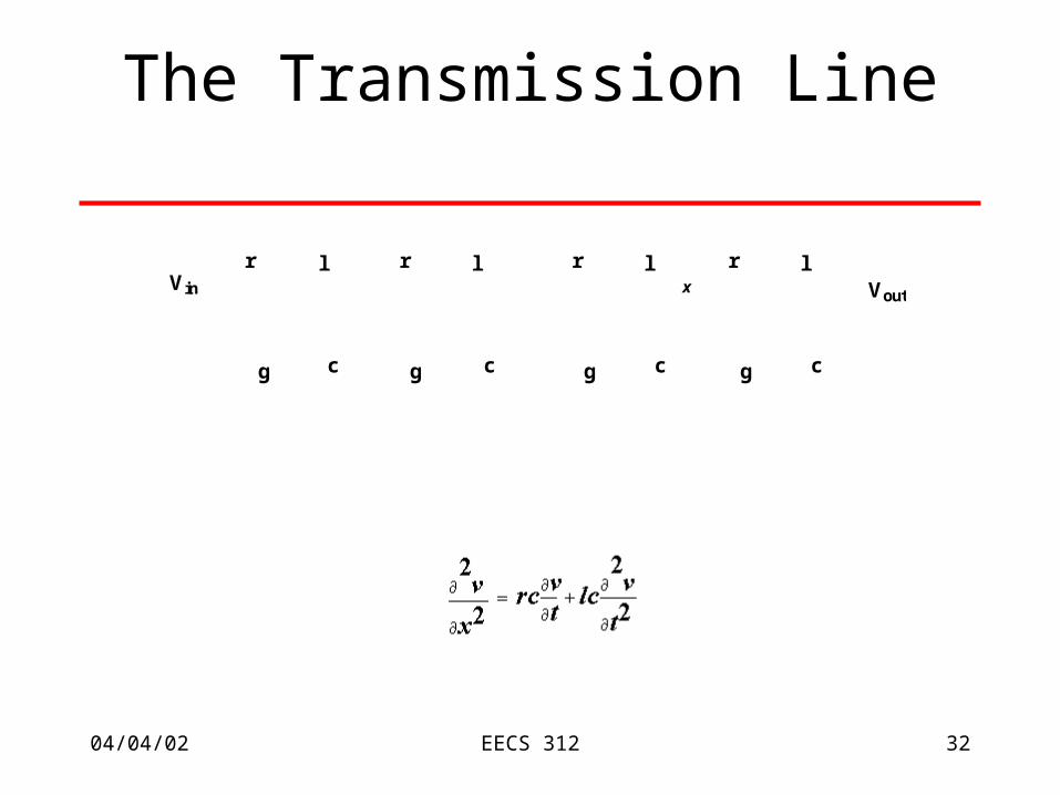
The Transmission Line
Vinr l
c
r l
c
r l
c
r l
c
Voutx
g g g g
04/04/02 EECS 312 33
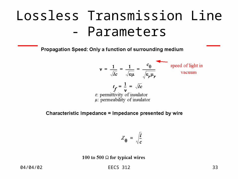
Lossless Transmission Line - Parameters
vacuumspeed of light in
04/04/02 EECS 312 34
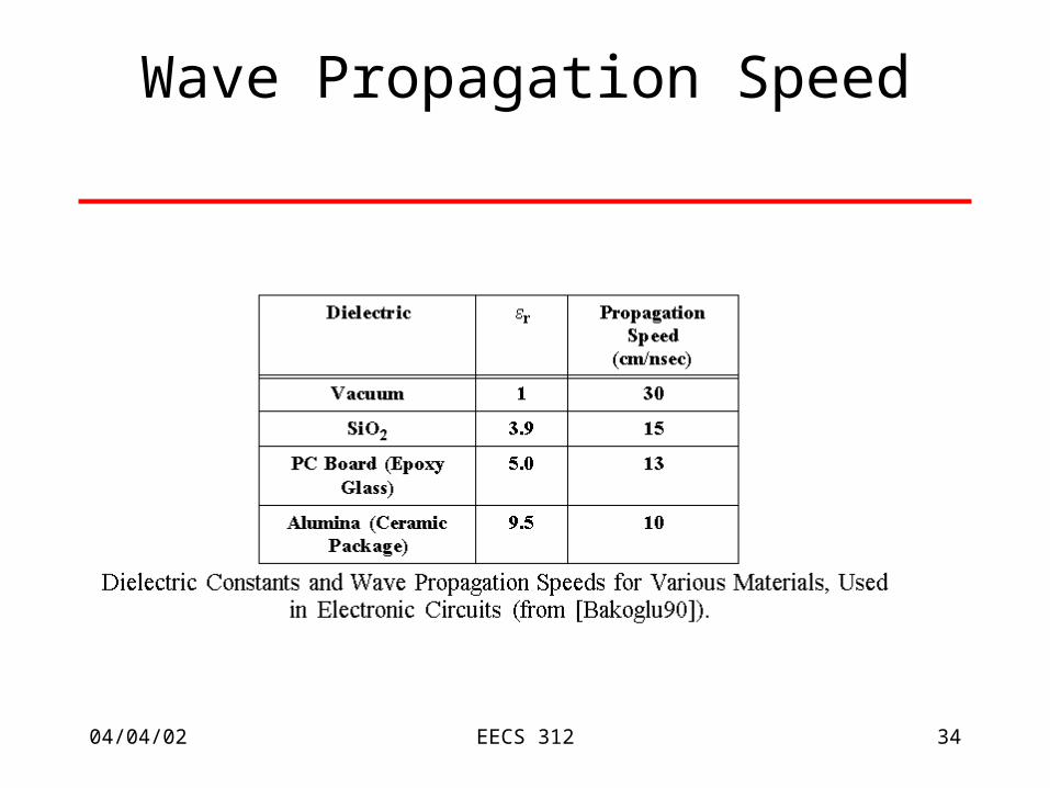
Wave Propagation Speed
04/04/02 EECS 312 35
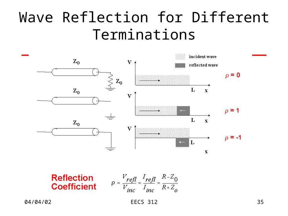
Wave Reflection for Different Terminations
04/04/02 EECS 312 36
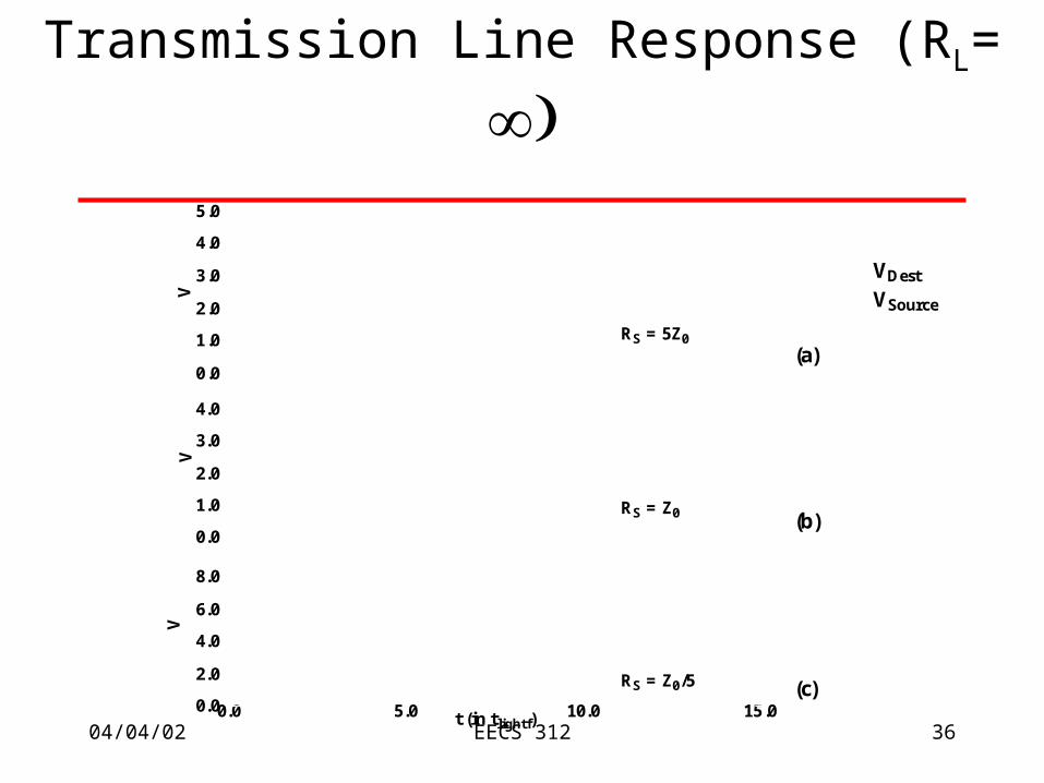
Transmission Line Response (RL=
0.0
1.0
2.0
3.0
4.0
5.0
V
0.0
1.0
2.0
3.0
4.0
V
0.0 5.0 10.0 15.0t (in tlightf)0.0
2.0
4.0
6.0
8.0
V
RS = 5Z0
RS = Z0
RS = Z0/5
(a)
(b)
(c)
VDestVSource
04/04/02 EECS 312 37
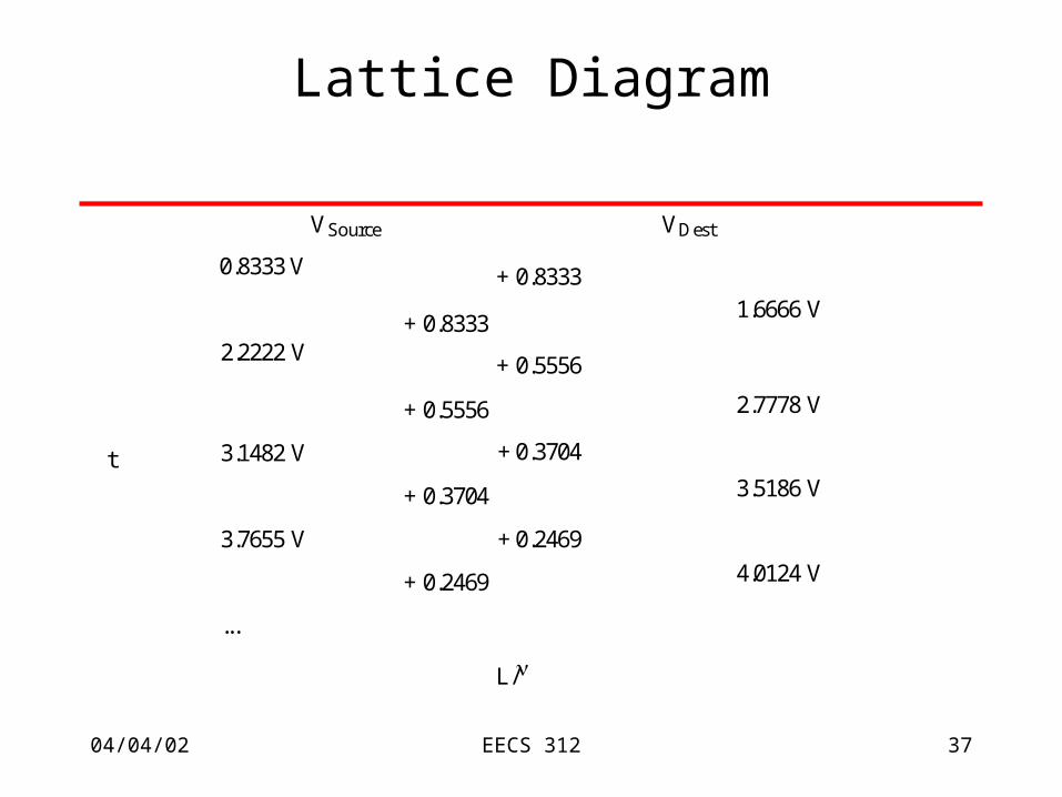
Lattice Diagram
VSource VDest
0.8333 V
1.6666 V
+ 0.8333
+ 0.8333
+ 0.5556
+ 0.5556
+ 0.3704
+ 0.2469
+ 0.3704
+ 0.2469
2.2222 V
3.1482 V
3.7655 V
...
2.7778 V
3.5186 V
4.0124 V
L/
t
04/04/02 EECS 312 38
When to Consider Transmission Line Effects?
Related Documents


![Paulo MoreiraTechnology1 Outline Introduction – “Is there a limit ?” Transistors – “CMOS building blocks” Parasitics I – “The [un]desirables” Parasitics.](https://static.cupdf.com/doc/110x72/56649d7e5503460f94a61dea/paulo-moreiratechnology1-outline-introduction-is-there-a-limit-.jpg)
