23.03.21 19:41 CSCI 150 Introduction to Digital and Computer System Design Lecture 4: Sequential Circuit V Jetic Gū

Welcome message from author
This document is posted to help you gain knowledge. Please leave a comment to let me know what you think about it! Share it to your friends and learn new things together.
Transcript

23.03.21 19:41CSCI 150 Introduction to Digital and Computer
System Design Lecture 4: Sequential Circuit V
Jetic Gū
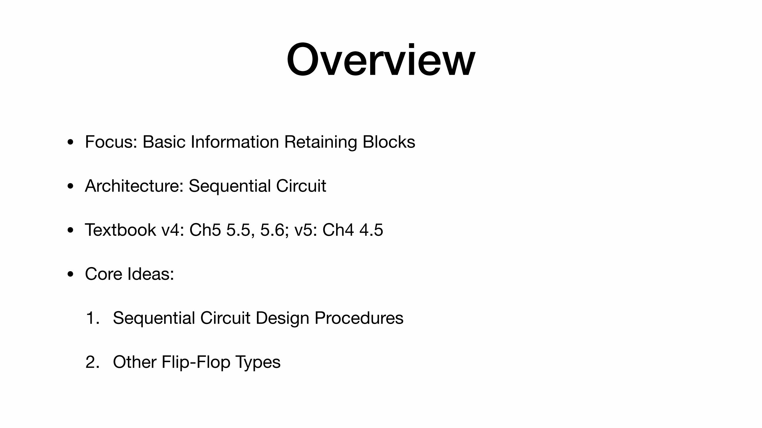
Overview• Focus: Basic Information Retaining Blocks
• Architecture: Sequential Circuit
• Textbook v4: Ch5 5.5, 5.6; v5: Ch4 4.5
• Core Ideas:
1. Sequential Circuit Design Procedures
2. Other Flip-Flop Types
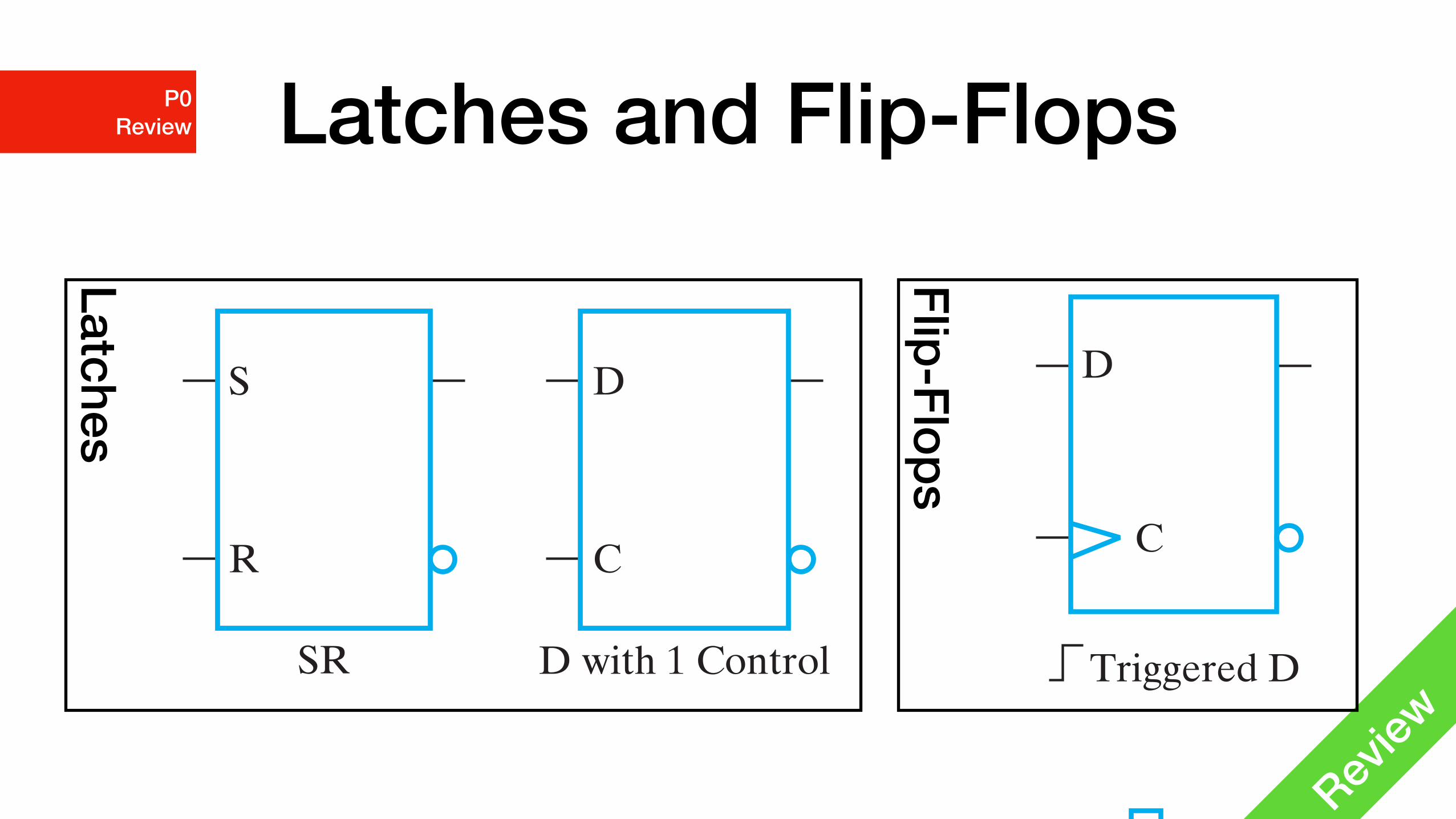
Latches and Flip-Flops
Review
P0 Review
Flip-Flops
4-3 / Flip-Flops 207
When the positive edge occurs, the clock input changes to 1. This disables the master latch so that its value is !xed and enables the slave latch so that it copies the state of the master latch. The state of the master latch to be copied is the state that is present at the positive edge of the clock. Thus, the behavior appears to be edge triggered. With the clock input equal to 1, the master latch is disabled and cannot change, so the state of both the master and the slave remain unchanged. Finally, when the clock input changes from 1 to 0, the master is enabled and begins following the D value. But during the 1- to- 0 transition, the slave is disabled before any change in the master can reach it. Thus, the value stored in the slave remains unchanged during this transition. An alternative implementation that requires fewer gates is given in Problem 4-3 at the end of the chapter.
Standard Graphics Symbols
The standard graphics symbols for the different types of latches and "ip- "ops are shown in Figure 4-11. A "ip- "op or latch is designated by a rectangular block with
(a) Latches
S
R
SR SR
S
R
D with 0 Control
D
C
D with 1 Control
D
C
(b) Master–slave flip-flops
D
C
Triggered DTriggered SR
S
R
C
D
C
Triggered DTriggered SR
S
R
C
(c) Edge-triggered flip-flops
Triggered D
D
C
Triggered D
D
C
FIGURE 4-11Standard Graphics Symbols for Latches and Flip- Flop
M04_MANO0637_05_SE_C04.indd 207 23/01/15 1:54 PM
Latches
4-3 / Flip-Flops 207
When the positive edge occurs, the clock input changes to 1. This disables the master latch so that its value is !xed and enables the slave latch so that it copies the state of the master latch. The state of the master latch to be copied is the state that is present at the positive edge of the clock. Thus, the behavior appears to be edge triggered. With the clock input equal to 1, the master latch is disabled and cannot change, so the state of both the master and the slave remain unchanged. Finally, when the clock input changes from 1 to 0, the master is enabled and begins following the D value. But during the 1- to- 0 transition, the slave is disabled before any change in the master can reach it. Thus, the value stored in the slave remains unchanged during this transition. An alternative implementation that requires fewer gates is given in Problem 4-3 at the end of the chapter.
Standard Graphics Symbols
The standard graphics symbols for the different types of latches and "ip- "ops are shown in Figure 4-11. A "ip- "op or latch is designated by a rectangular block with
(a) Latches
S
R
SR SR
S
R
D with 0 Control
D
C
D with 1 Control
D
C
(b) Master–slave flip-flops
D
C
Triggered DTriggered SR
S
R
C
D
C
Triggered DTriggered SR
S
R
C
(c) Edge-triggered flip-flops
Triggered D
D
C
Triggered D
D
C
FIGURE 4-11Standard Graphics Symbols for Latches and Flip- Flop
M04_MANO0637_05_SE_C04.indd 207 23/01/15 1:54 PM

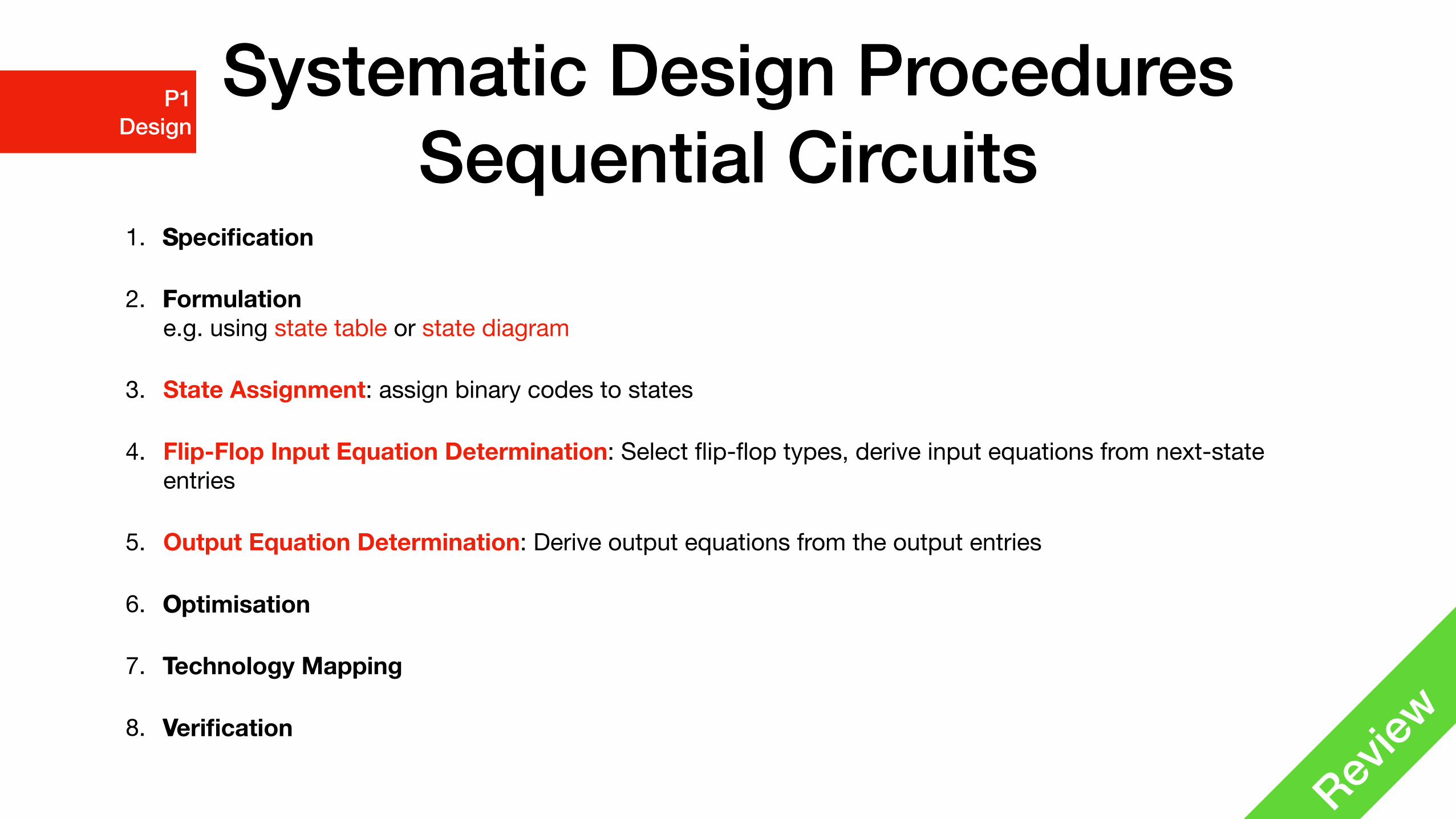
Systematic Design Procedures Sequential Circuits
1. Specification
2. Formulatione.g. using state table or state diagram
3. State Assignment: assign binary codes to states
4. Flip-Flop Input Equation Determination: Select flip-flop types, derive input equations from next-state entries
5. Output Equation Determination: Derive output equations from the output entries
6. Optimisation
7. Technology Mapping
8. Verification
Review
P0 Review
Systematic Design ProceduresSequential Circuits
Specification
Formulation
Optimisation
Technology Mapping
Verification
Sequential Circuit Design II
Summary
P1 Design
State Assignment; Input Equation Determination; Output Equation Determination
Systematic Design Procedures Sequential Circuits
1. Specification
2. Formulatione.g. using state table or state diagram
3. State Assignment: assign binary codes to states
4. Flip-Flop Input Equation Determination: Select flip-flop types, derive input equations from next-state entries
5. Output Equation Determination: Derive output equations from the output entries
6. Optimisation
7. Technology Mapping
8. Verification
Review
P1 Design
Systematic Design ProceduresSequential Circuits
Specification
Formulation
Optimisation
Technology Mapping
Verification
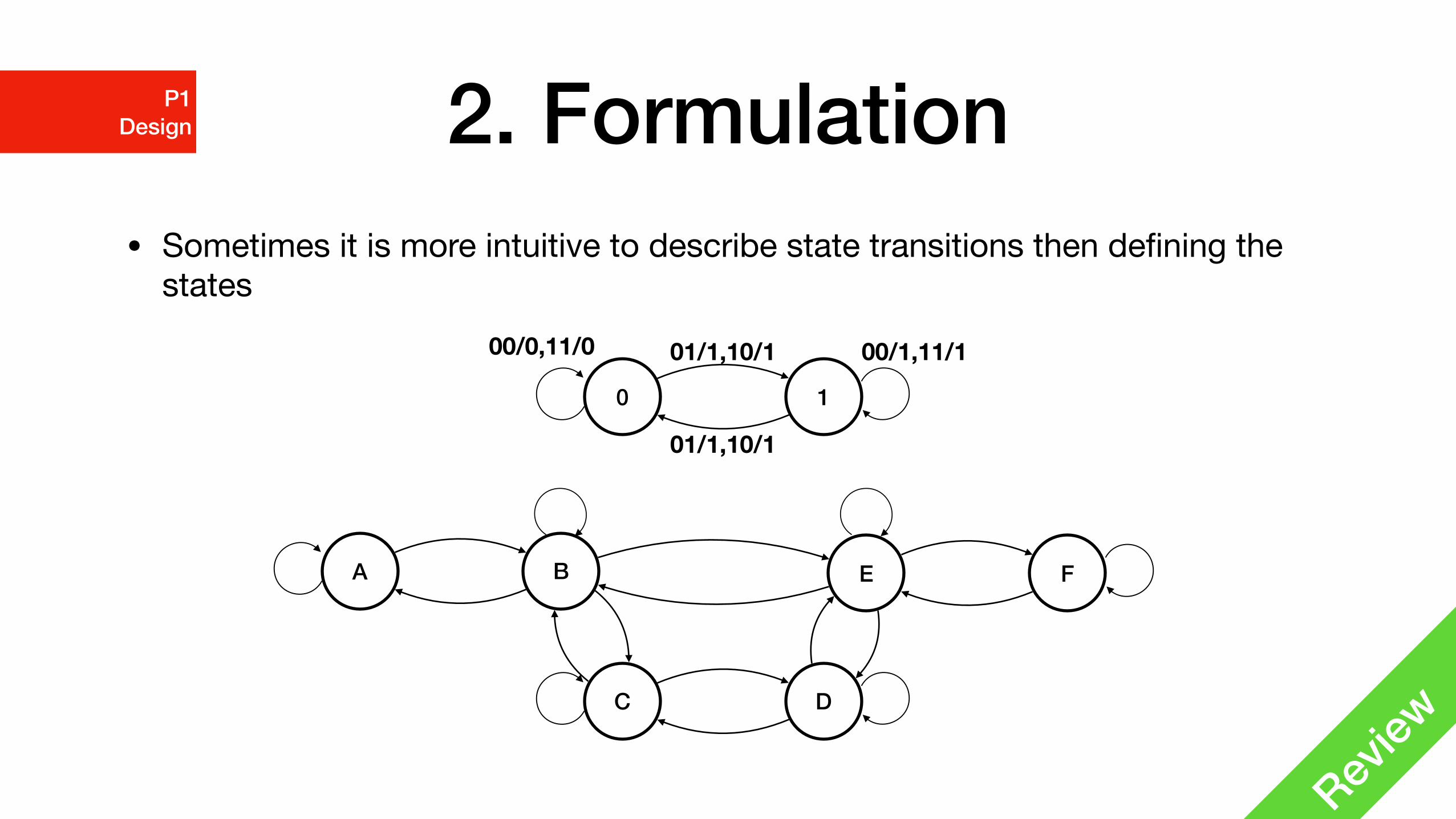
2. Formulation• Sometimes it is more intuitive to describe state transitions then defining the
states
Review
P1 Design
0 1
01/1,10/1
01/1,10/1
00/0,11/0 00/1,11/1
C D
A B E F
2. Formulation
Example
P1 Design
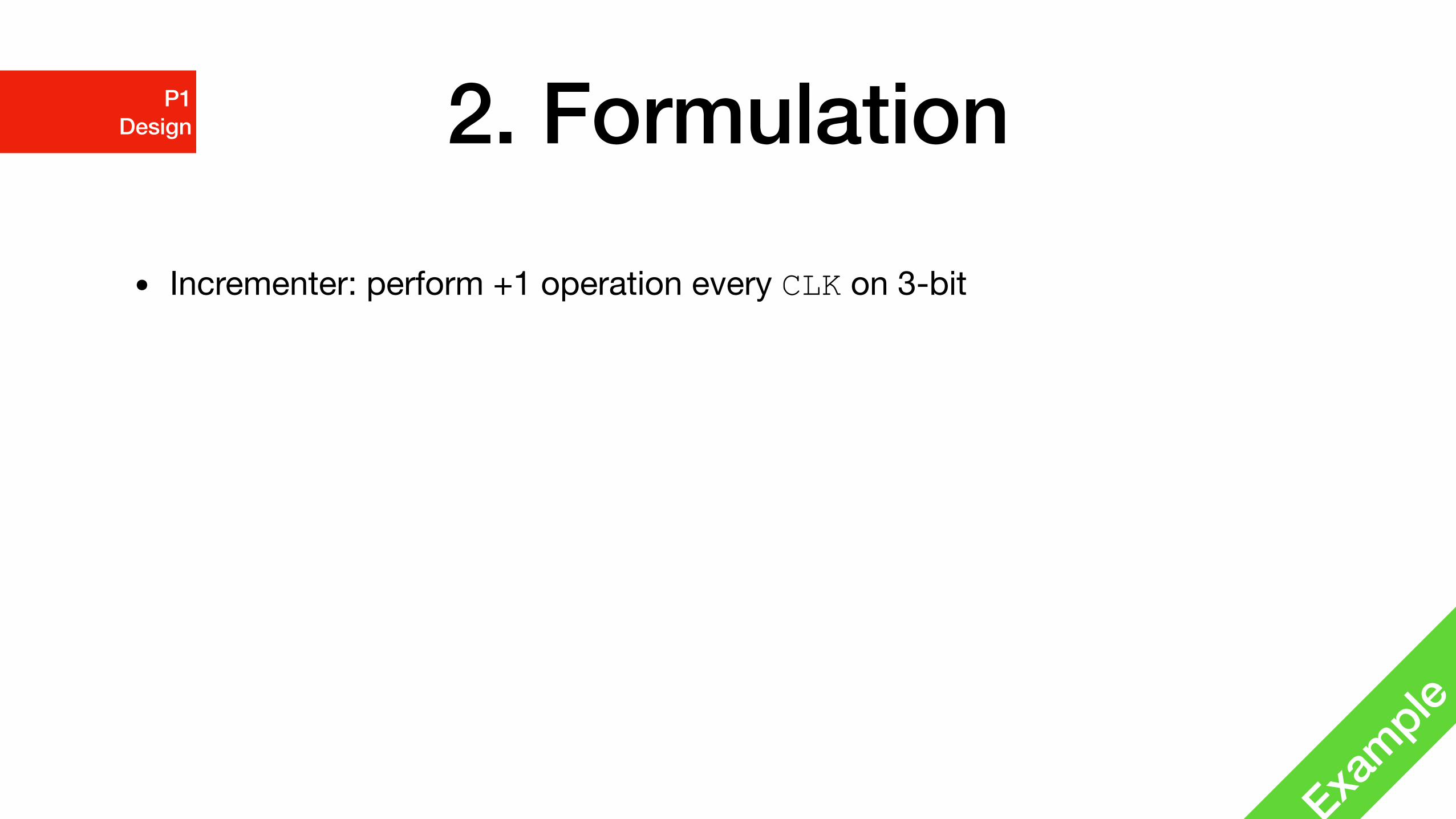
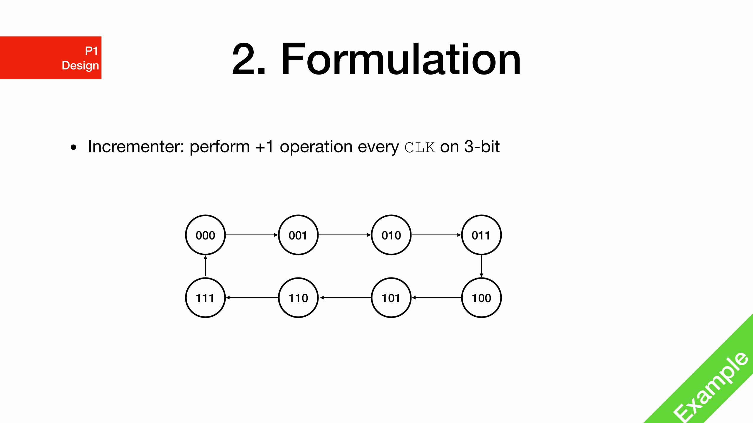
• Incrementer: perform +1 operation every CLK on 3-bit
2. Formulation
Example
P1 Design
• Incrementer: perform +1 operation every CLK on 3-bit
000 001 010 011
111 110 101 100
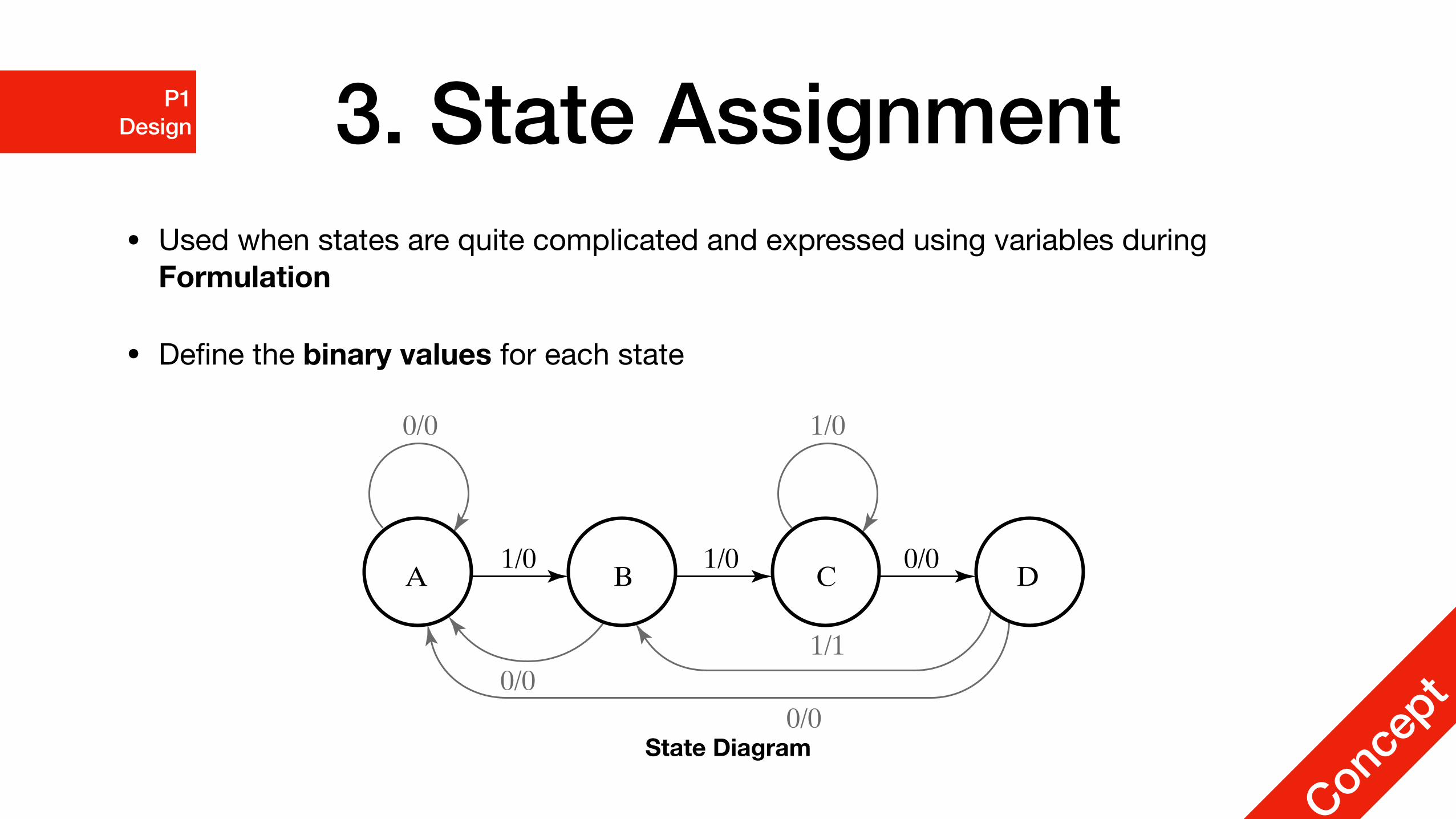
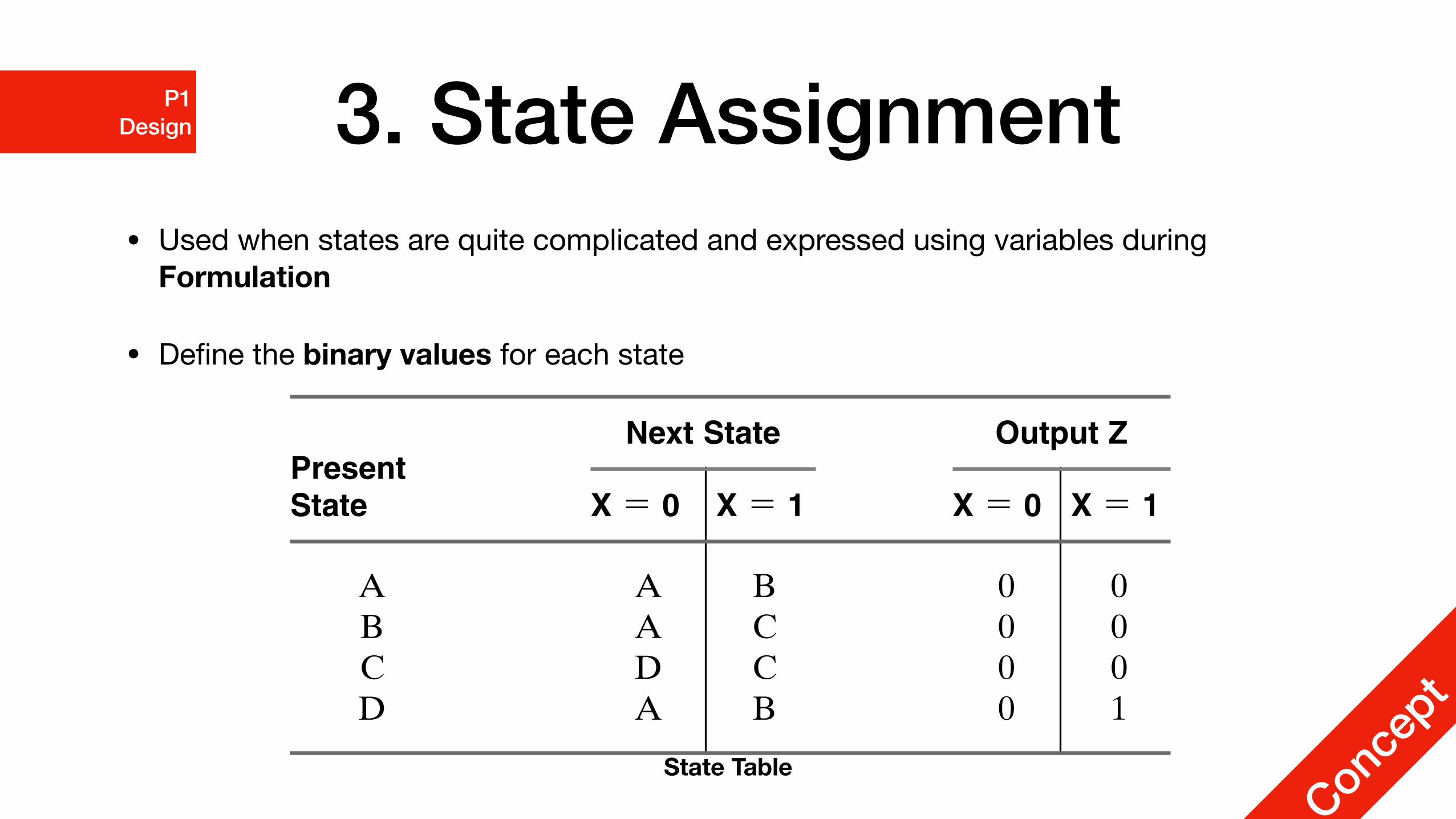
3. State Assignment• Used when states are quite complicated and expressed using variables during
Formulation
• Define the binary values for each state
Concep
t
P1 Design
SEQUENTIAL CIRCUITS
equal to 1 when the previous three inputs to the circuit were 110 and current inputis a 1. Otherwise, Z equals 0.
The first step in the formulation process is to determine whether the statediagram or table must be a Mealy model or Moore model circuit. The portion ofthe preceding specification that says “... making Z equal to 1 when the previousthree inputs to the circuit are 110 and the current input is a 1” implies that the out-put is determined from not only the current state, but also the current input. As aconsequence, a Mealy model circuit with the output dependent on both state andinputs is required.
Recall that a key factor in the formulation of any state diagram is to recog-nize that states are used to “remember” something about the history of the inputs.For example, for the sequence 1101 to be able to produce the output value 1 coin-cident with the final 1 in the sequence, the circuit must be in a state that “remem-bers” that the previous three inputs were 110. With this concept in mind, we beginto formulate the state diagram by defining an arbitrary initial state A as the resetstate and the state in which “none of the sequence to be recognized has occurred.”If a 1 occurs on the input, since 1 is the first bit in the sequence, this event must be“remembered,” and the state after the clock pulse cannot be A. So a second state,B, is established to represent the occurrence of the first 1 in the sequence. Further,to represent the occurrence of the first 1 in the sequence, a transition is placedfrom A to B and labeled with a 1. Since this is not the final 1 in the sequence 1101,its output is a 0. This initial portion of the state diagram is given in Figure 20(a).
(a)
1/0A B
(b)
1/0 1/0A CB
(c)
1/0 1/0 0/0 1/1A C DB
(d)
1/0 1/0 0/0
1/0
1/1
0/0
0/00/0
A C DB
FIGURE 20Construction of a State Diagram for Example 4
���
State Diagram
3. State Assignment• Used when states are quite complicated and expressed using variables during
Formulation
• Define the binary values for each state
Concep
t
P1 Design
SEQUENTIAL CIRCUITS
interested student, state-minimization procedures are found in Reference 1 at theend of the chapter as well as in many other logic design texts.
The next example illustrates an additional method for avoiding extra statesby recognizing potential state equivalence during the design process.
EXAMPLE 4 Finding a State Diagram for a BCD–to–Excess-3 Decoder
Consider a BCD–to–excess-3 decoder where the inputs, rather than being pre-sented to the circuit simultaneously, are presented serially in successive clockcycles, least significant bit first. In Table 4(a), the input sequences and correspond-ing output sequences are listed with the least significant bit first. For example,
TABLE 3State Table for State Diagram in Figure 20
Present State
Next State Output Z
X ! 0 X ! 1 X ! 0 X ! 1
ABCD
AADA
BCCB
0000
0001
TABLE 4Sequence Tables for Code-Converter Example
(a) Sequences in Order ofDigits Represented
(b) Sequences in Order ofCommon Prefixes
BCD Input Excess-3 Output BCD Input Excess-3 Output
1 2 3 4 1 2 3 4 1 2 3 4 1 2 3 4
0101010101
0011001100
0000111100
0000000011
1010101010
1001100110
0111100001
0000011111
0000011111
0001100011
0010100101
0100001000
1111100000
1110000011
0011011010
0100101101
���
State Table
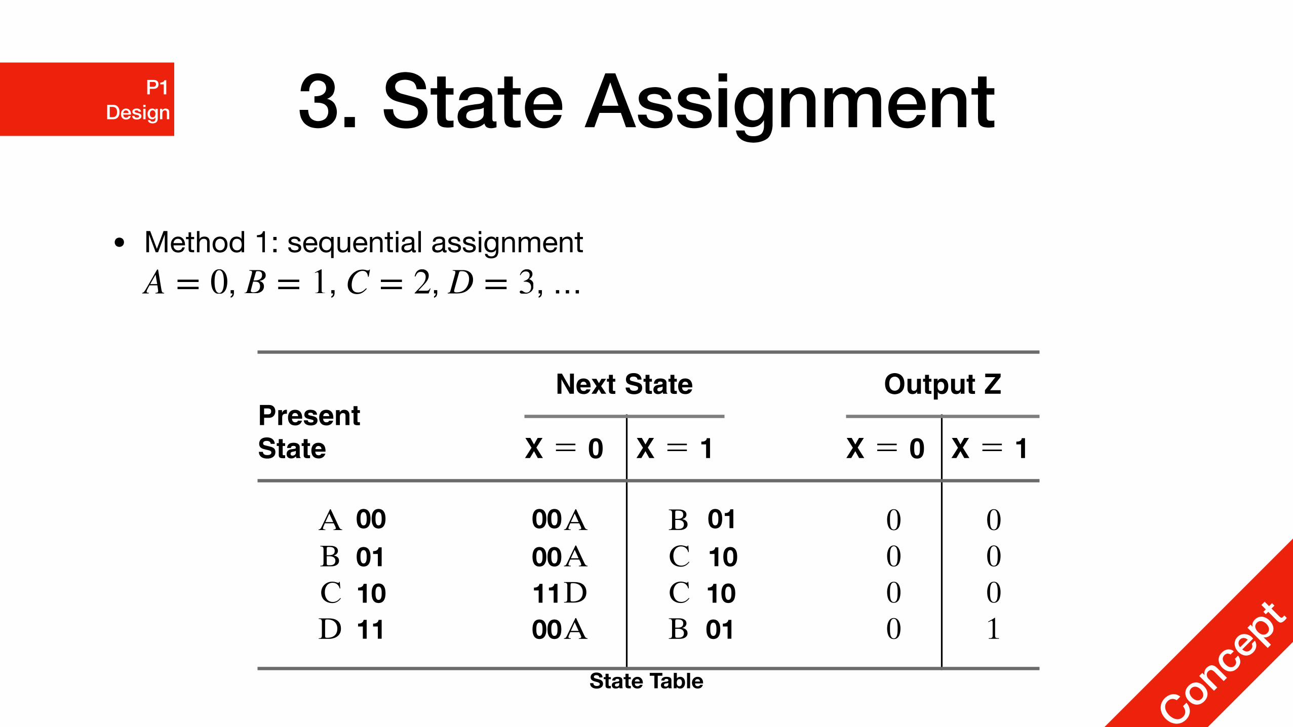
3. State Assignment• Method 1: sequential assignment
, , , , …A = 0 B = 1 C = 2 D = 3
Concep
t
P1 Design
SEQUENTIAL CIRCUITS
interested student, state-minimization procedures are found in Reference 1 at theend of the chapter as well as in many other logic design texts.
The next example illustrates an additional method for avoiding extra statesby recognizing potential state equivalence during the design process.
EXAMPLE 4 Finding a State Diagram for a BCD–to–Excess-3 Decoder
Consider a BCD–to–excess-3 decoder where the inputs, rather than being pre-sented to the circuit simultaneously, are presented serially in successive clockcycles, least significant bit first. In Table 4(a), the input sequences and correspond-ing output sequences are listed with the least significant bit first. For example,
TABLE 3State Table for State Diagram in Figure 20
Present State
Next State Output Z
X ! 0 X ! 1 X ! 0 X ! 1
ABCD
AADA
BCCB
0000
0001
TABLE 4Sequence Tables for Code-Converter Example
(a) Sequences in Order ofDigits Represented
(b) Sequences in Order ofCommon Prefixes
BCD Input Excess-3 Output BCD Input Excess-3 Output
1 2 3 4 1 2 3 4 1 2 3 4 1 2 3 4
0101010101
0011001100
0000111100
0000000011
1010101010
1001100110
0111100001
0000011111
0000011111
0001100011
0010100101
0100001000
1111100000
1110000011
0011011010
0100101101
���
State Table
00 000001
10 1111 00
101001
01
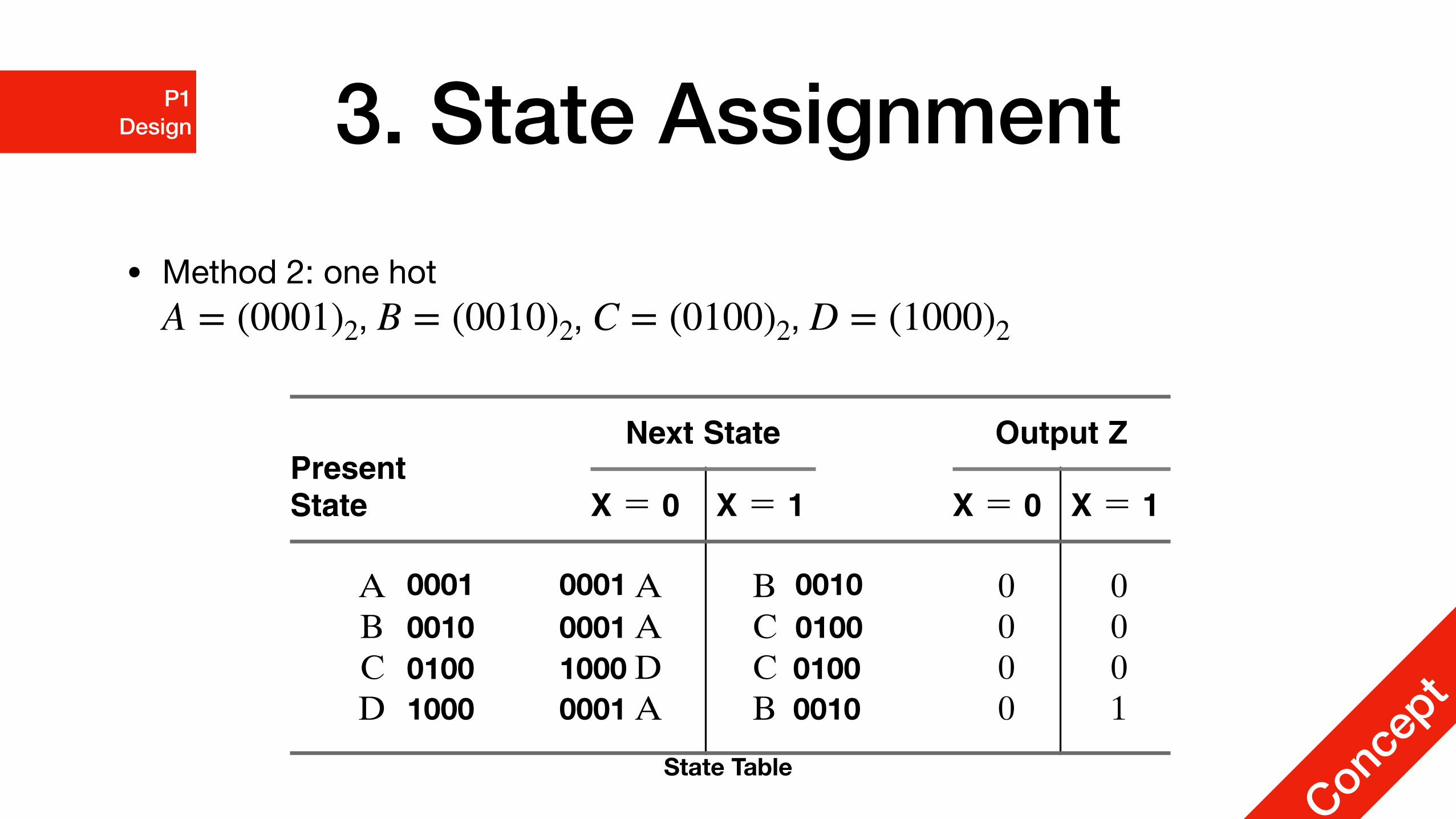
3. State Assignment• Method 2: one hot
, , , A = (0001)2 B = (0010)2 C = (0100)2 D = (1000)2
Concep
t
P1 Design
SEQUENTIAL CIRCUITS
interested student, state-minimization procedures are found in Reference 1 at theend of the chapter as well as in many other logic design texts.
The next example illustrates an additional method for avoiding extra statesby recognizing potential state equivalence during the design process.
EXAMPLE 4 Finding a State Diagram for a BCD–to–Excess-3 Decoder
Consider a BCD–to–excess-3 decoder where the inputs, rather than being pre-sented to the circuit simultaneously, are presented serially in successive clockcycles, least significant bit first. In Table 4(a), the input sequences and correspond-ing output sequences are listed with the least significant bit first. For example,
TABLE 3State Table for State Diagram in Figure 20
Present State
Next State Output Z
X ! 0 X ! 1 X ! 0 X ! 1
ABCD
AADA
BCCB
0000
0001
TABLE 4Sequence Tables for Code-Converter Example
(a) Sequences in Order ofDigits Represented
(b) Sequences in Order ofCommon Prefixes
BCD Input Excess-3 Output BCD Input Excess-3 Output
1 2 3 4 1 2 3 4 1 2 3 4 1 2 3 4
0101010101
0011001100
0000111100
0000000011
1010101010
1001100110
0111100001
0000011111
0000011111
0001100011
0010100101
0100001000
1111100000
1110000011
0011011010
0100101101
���
State Table
0001 000100010010
0100 10001000 0001
010001000010
0010

3. State Assignment
• Are these the only methods?
• No, there’s tons
• Are these methods equivalent?
• No, they each lead to completely different solutions, with different costs
• For this course, we don’t require you to come up with the best state assignment solution
Think
P1 Design

3. State Assignment
Think
P1 Design

3. State Assignment
• Are we using all of the combinations?
Think
P1 Design

3. State Assignment
• Are we using all of the combinations?
• No. Some states are not designed to be reachable
Think
P1 Design

3. State Assignment
• Are we using all of the combinations?
• No. Some states are not designed to be reachable
• Could also be used in the future for extensions
Think
P1 Design
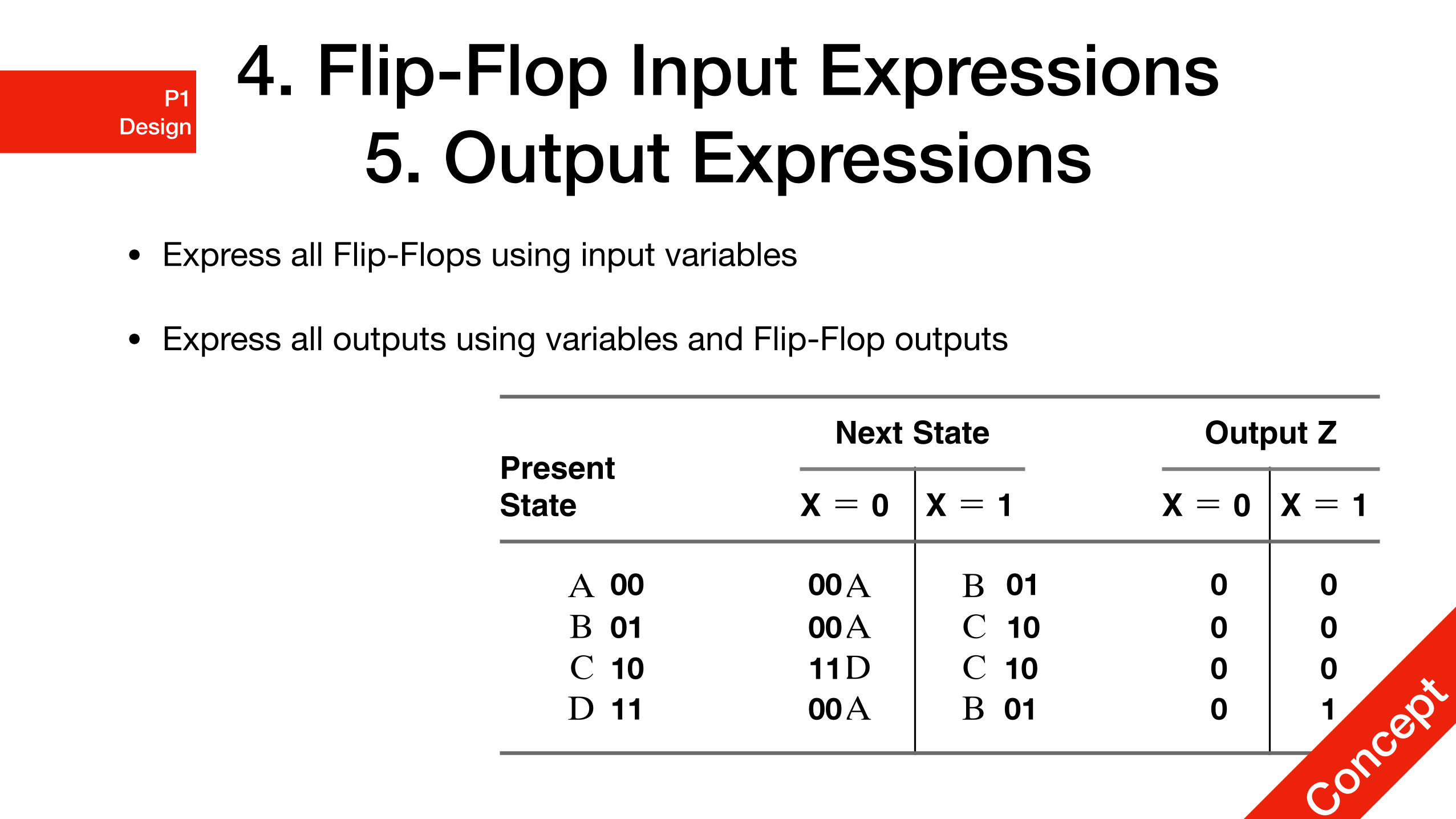
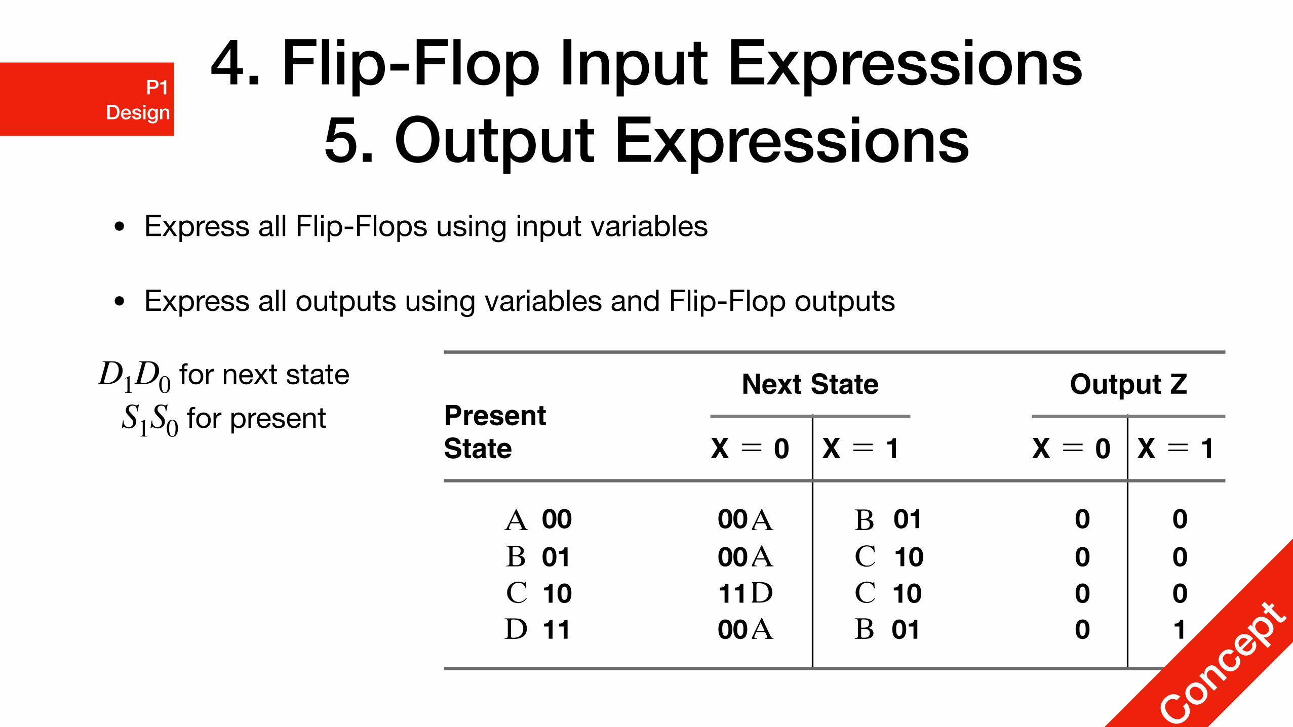
4. Flip-Flop Input Expressions 5. Output Expressions
• Express all Flip-Flops using input variables
• Express all outputs using variables and Flip-Flop outputs
P1 Design
SEQUENTIAL CIRCUITS
interested student, state-minimization procedures are found in Reference 1 at theend of the chapter as well as in many other logic design texts.
The next example illustrates an additional method for avoiding extra statesby recognizing potential state equivalence during the design process.
EXAMPLE 4 Finding a State Diagram for a BCD–to–Excess-3 Decoder
Consider a BCD–to–excess-3 decoder where the inputs, rather than being pre-sented to the circuit simultaneously, are presented serially in successive clockcycles, least significant bit first. In Table 4(a), the input sequences and correspond-ing output sequences are listed with the least significant bit first. For example,
TABLE 3State Table for State Diagram in Figure 20
Present State
Next State Output Z
X ! 0 X ! 1 X ! 0 X ! 1
ABCD
AADA
BCCB
0000
0001
TABLE 4Sequence Tables for Code-Converter Example
(a) Sequences in Order ofDigits Represented
(b) Sequences in Order ofCommon Prefixes
BCD Input Excess-3 Output BCD Input Excess-3 Output
1 2 3 4 1 2 3 4 1 2 3 4 1 2 3 4
0101010101
0011001100
0000111100
0000000011
1010101010
1001100110
0111100001
0000011111
0000011111
0001100011
0010100101
0100001000
1111100000
1110000011
0011011010
0100101101
���
00011011
00001100
101001
01
0000
0001
Concep
t
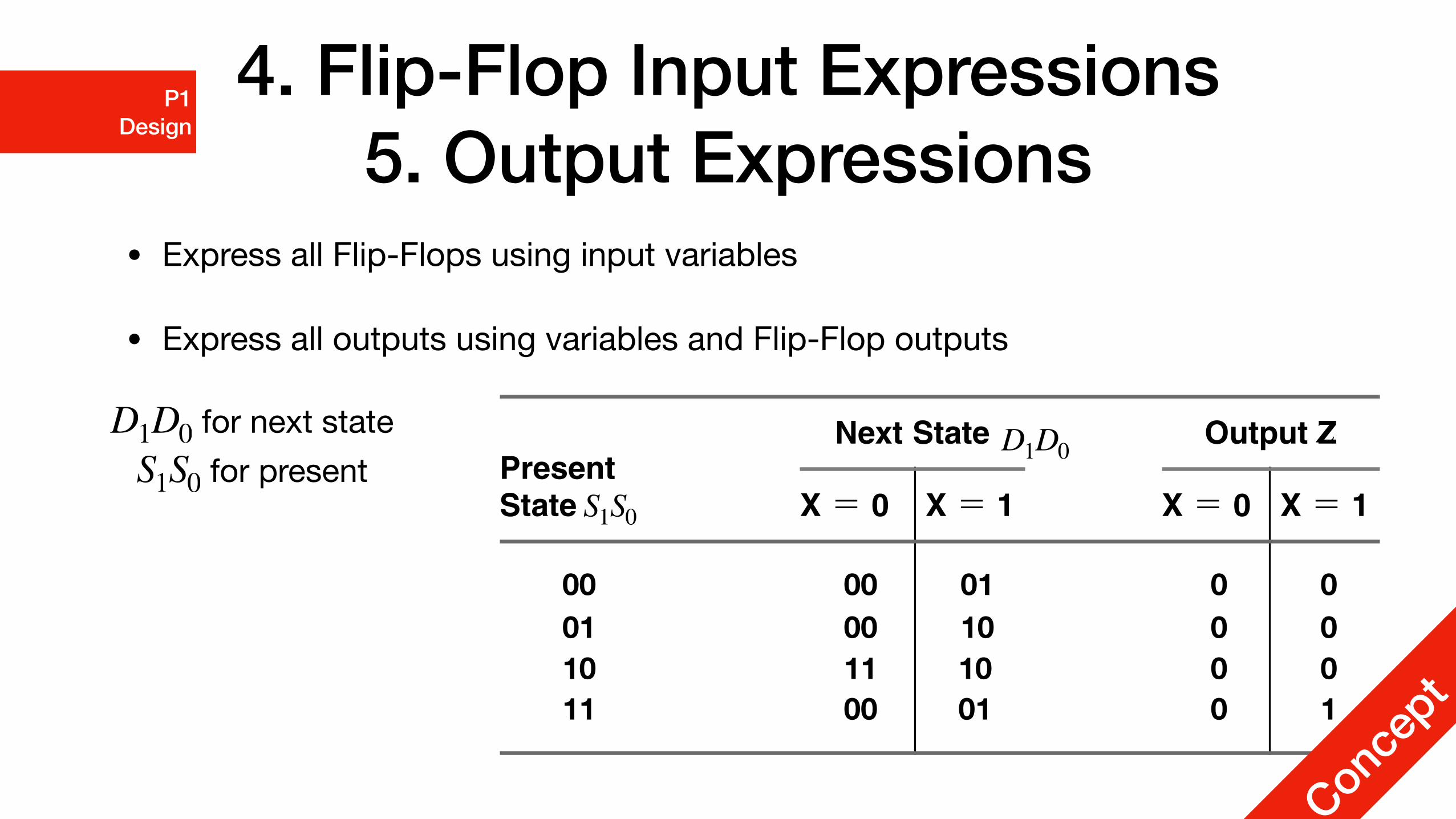
4. Flip-Flop Input Expressions 5. Output Expressions
• Express all Flip-Flops using input variables
• Express all outputs using variables and Flip-Flop outputs
P1 Design
SEQUENTIAL CIRCUITS
interested student, state-minimization procedures are found in Reference 1 at theend of the chapter as well as in many other logic design texts.
The next example illustrates an additional method for avoiding extra statesby recognizing potential state equivalence during the design process.
EXAMPLE 4 Finding a State Diagram for a BCD–to–Excess-3 Decoder
Consider a BCD–to–excess-3 decoder where the inputs, rather than being pre-sented to the circuit simultaneously, are presented serially in successive clockcycles, least significant bit first. In Table 4(a), the input sequences and correspond-ing output sequences are listed with the least significant bit first. For example,
TABLE 3State Table for State Diagram in Figure 20
Present State
Next State Output Z
X ! 0 X ! 1 X ! 0 X ! 1
ABCD
AADA
BCCB
0000
0001
TABLE 4Sequence Tables for Code-Converter Example
(a) Sequences in Order ofDigits Represented
(b) Sequences in Order ofCommon Prefixes
BCD Input Excess-3 Output BCD Input Excess-3 Output
1 2 3 4 1 2 3 4 1 2 3 4 1 2 3 4
0101010101
0011001100
0000111100
0000000011
1010101010
1001100110
0111100001
0000011111
0000011111
0001100011
0010100101
0100001000
1111100000
1110000011
0011011010
0100101101
���
00011011
00001100
101001
01
for next state for present
D1D0S1S0
0000
0001
Concep
t
4. Flip-Flop Input Expressions 5. Output Expressions
• Express all Flip-Flops using input variables
• Express all outputs using variables and Flip-Flop outputs
P1 Design
SEQUENTIAL CIRCUITS
interested student, state-minimization procedures are found in Reference 1 at theend of the chapter as well as in many other logic design texts.
The next example illustrates an additional method for avoiding extra statesby recognizing potential state equivalence during the design process.
EXAMPLE 4 Finding a State Diagram for a BCD–to–Excess-3 Decoder
Consider a BCD–to–excess-3 decoder where the inputs, rather than being pre-sented to the circuit simultaneously, are presented serially in successive clockcycles, least significant bit first. In Table 4(a), the input sequences and correspond-ing output sequences are listed with the least significant bit first. For example,
TABLE 3State Table for State Diagram in Figure 20
Present State
Next State Output Z
X ! 0 X ! 1 X ! 0 X ! 1
ABCD
AADA
BCCB
0000
0001
TABLE 4Sequence Tables for Code-Converter Example
(a) Sequences in Order ofDigits Represented
(b) Sequences in Order ofCommon Prefixes
BCD Input Excess-3 Output BCD Input Excess-3 Output
1 2 3 4 1 2 3 4 1 2 3 4 1 2 3 4
0101010101
0011001100
0000111100
0000000011
1010101010
1001100110
0111100001
0000011111
0000011111
0001100011
0010100101
0100001000
1111100000
1110000011
0011011010
0100101101
���
00011011
00001100
101001
01
for next state for present
D1D0S1S0
D1D0
S1S0
0000
0001
Concep
t
Z
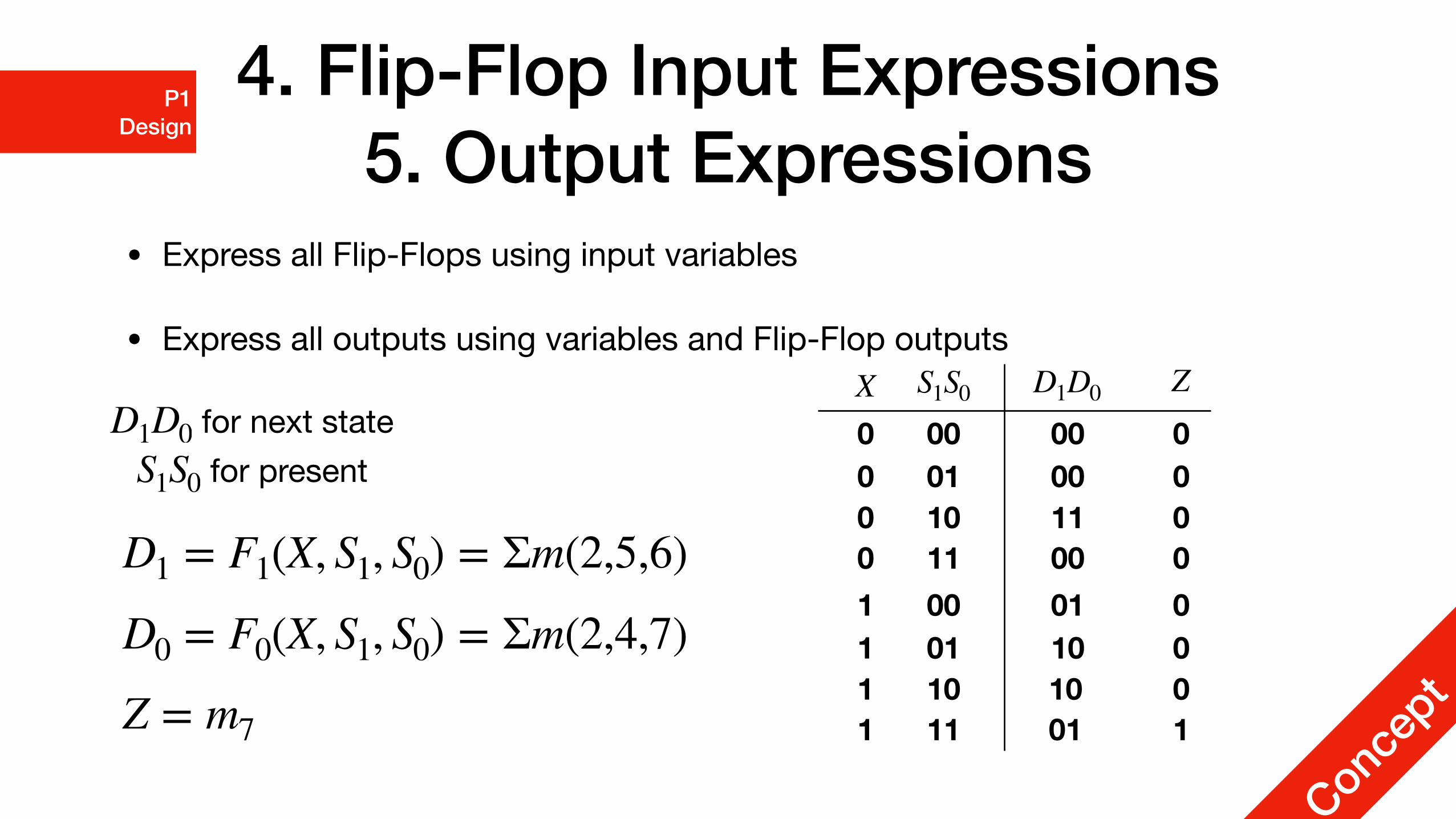
4. Flip-Flop Input Expressions 5. Output Expressions
• Express all Flip-Flops using input variables
• Express all outputs using variables and Flip-Flop outputs
P1 Design
00011011
00001100
101001
01
for next state for present
D1D0S1S0
D1D0S1S0
00000001
Concep
t
Z
00011011
X00001111
D1 = F1(X, S1, S0) = Σm(2,5,6)
D0 = F0(X, S1, S0) = Σm(2,4,7)
Z = m7
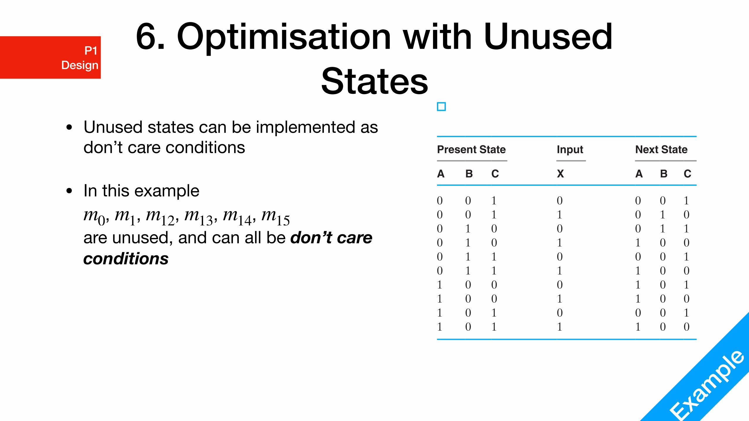
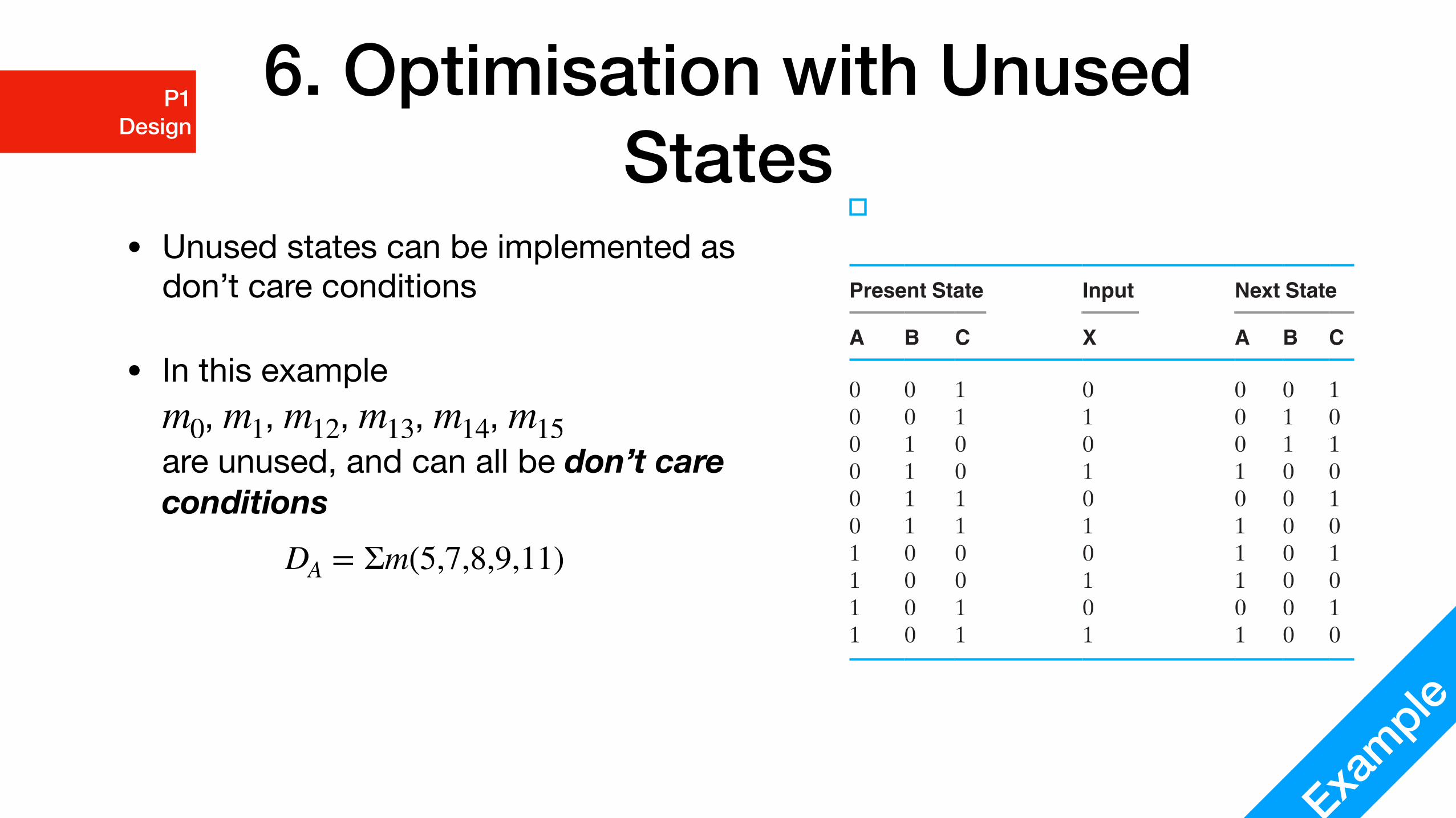
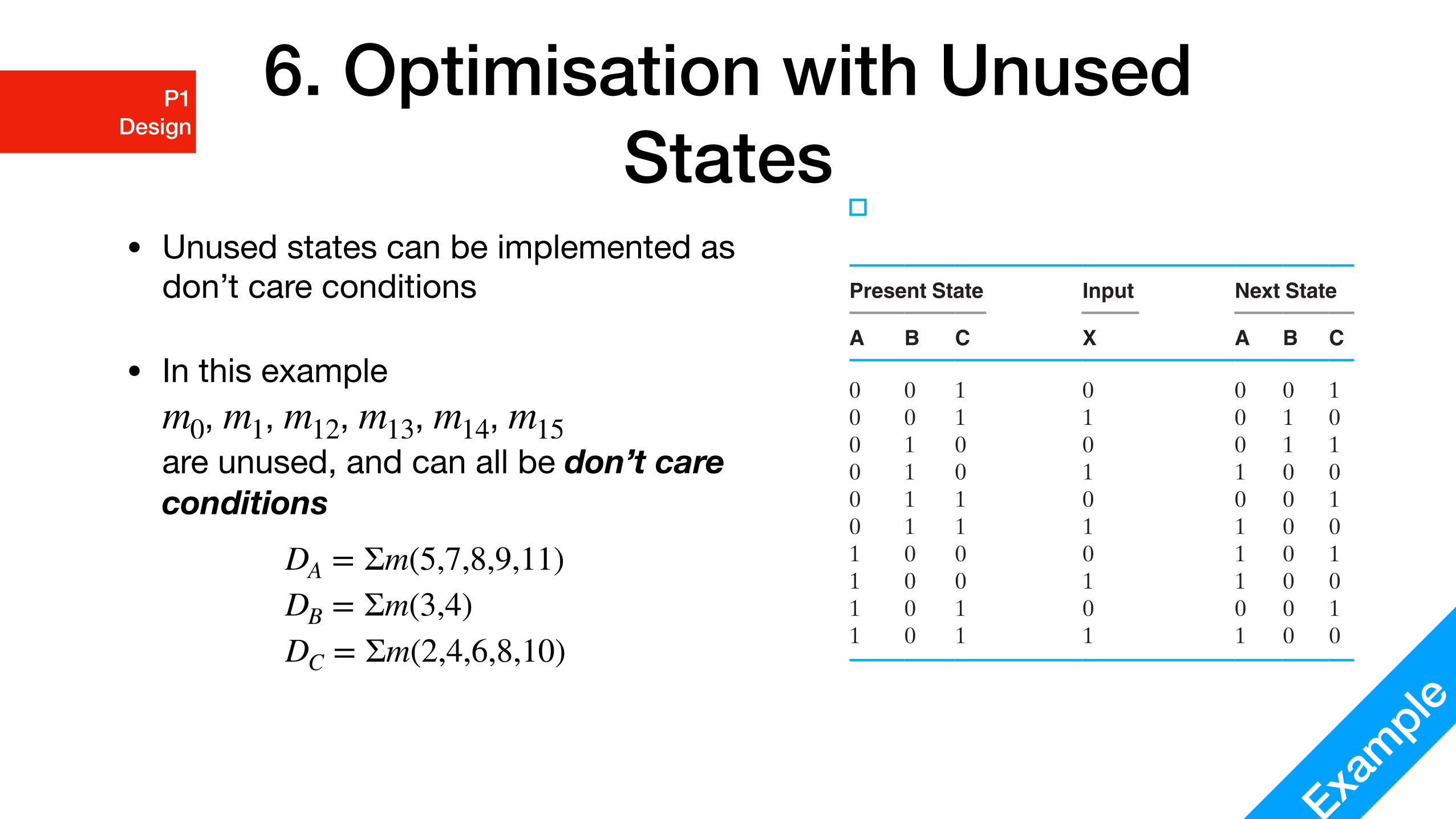
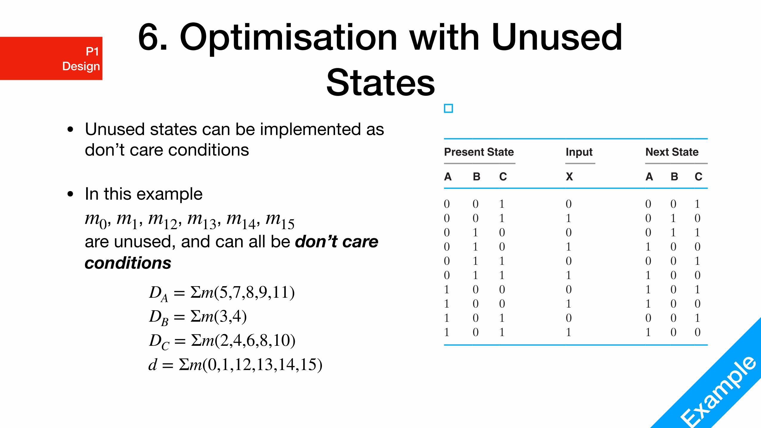
6. Optimisation with Unused States
• Unused states can be implemented as don’t care conditions
• In this example, , , , ,
are unused, and can all be don’t care conditions
m0 m1 m12 m13 m14 m15
Example
P1 Design 4-5 / Sequential Circuit Design 231
The three input equations for the D !ip- !ops are derived from the next- state values and are simpli"ed in the maps of Figure 4-23. Each map has six don’ t- care minterms in the squares corresponding to binary 0, 1, 12, 13, 14, and 15. The opti-mized equations are
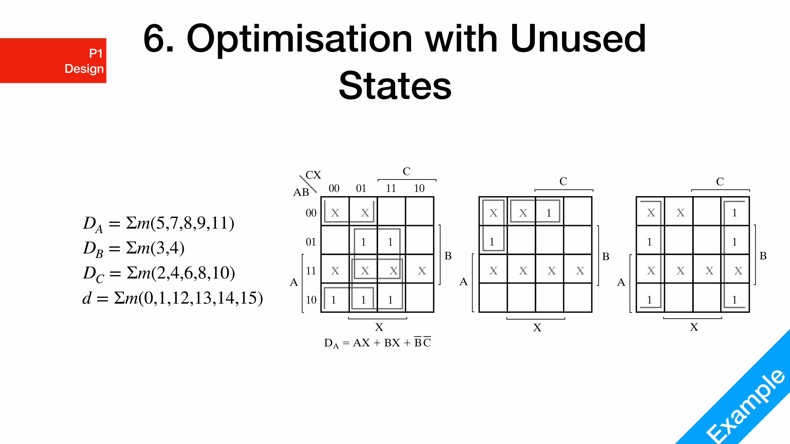
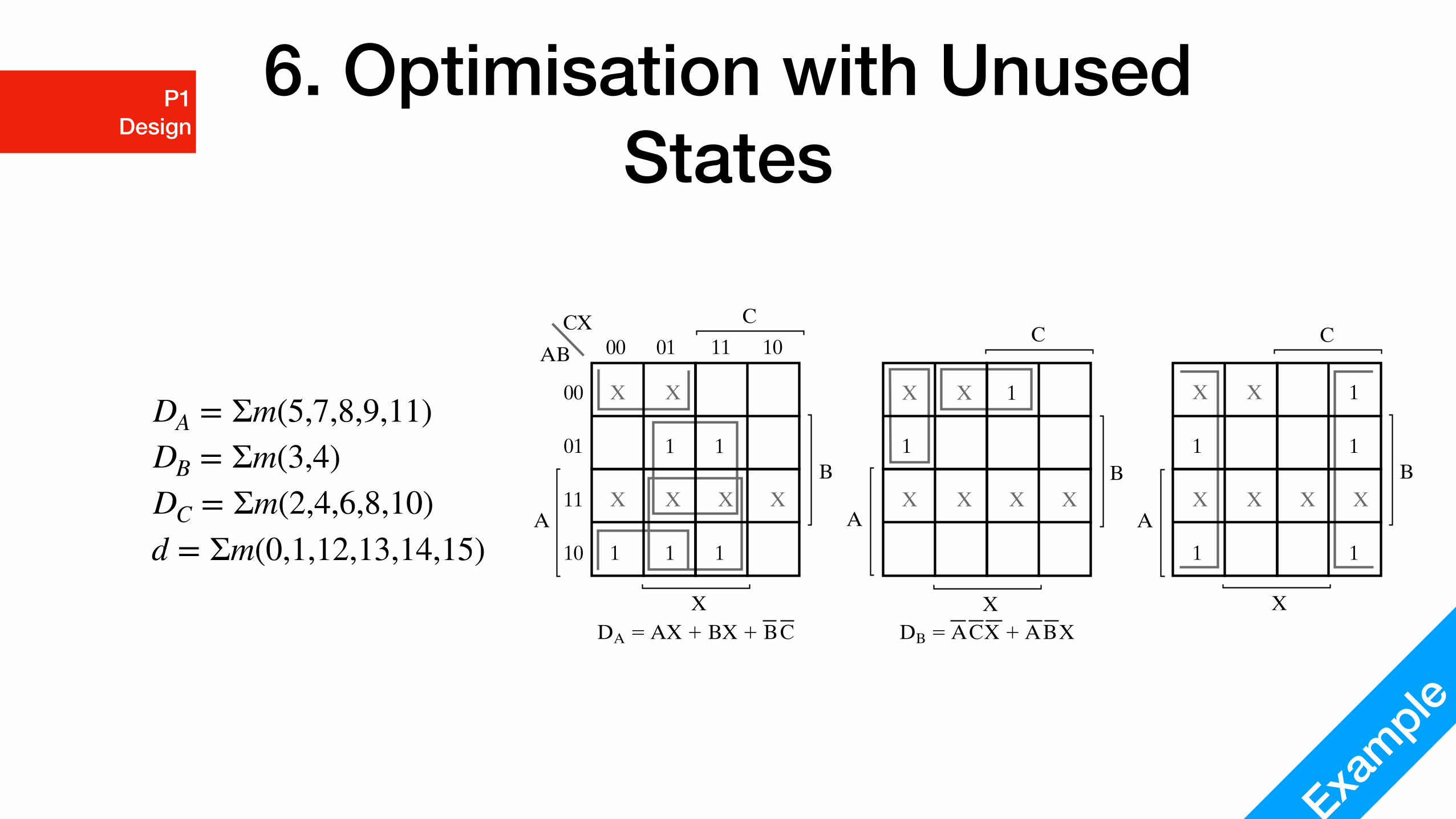
DA = AX + BX + B C
DB = A C X + A BX
DC = X
The logic diagram can be obtained directly from the input equations and will not be drawn here.
It is possible that outside interference or a malfunction will cause the circuit to enter one of the unused states. Thus, it is sometimes desirable to specify, fully or at least
TABLE 4-7State Table for Designing with Unused States
Present State Input Next State
A B C X A B C
0 0 1 0 0 0 10 0 1 1 0 1 00 1 0 0 0 1 10 1 0 1 1 0 00 1 1 0 0 0 10 1 1 1 1 0 01 0 0 0 1 0 11 0 0 1 1 0 01 0 1 0 0 0 11 0 1 1 1 0 0
00
01
00 01CX
AB 11 10
11
10
X
C
X
A
B
X
1 1
X XX X
1 11
XX
1
1
X XX X
C
X
A
B
XX
1
X XX X
1
1
1
1
C
X
A
B
FIGURE 4-23Maps for Optimizing Input Equations
M04_MANO0637_05_SE_C04.indd 231 23/01/15 1:54 PM
6. Optimisation with Unused States
• Unused states can be implemented as don’t care conditions
• In this example, , , , ,
are unused, and can all be don’t care conditions
m0 m1 m12 m13 m14 m15
Example
P1 Design 4-5 / Sequential Circuit Design 231
The three input equations for the D !ip- !ops are derived from the next- state values and are simpli"ed in the maps of Figure 4-23. Each map has six don’ t- care minterms in the squares corresponding to binary 0, 1, 12, 13, 14, and 15. The opti-mized equations are
DA = AX + BX + B C
DB = A C X + A BX
DC = X
The logic diagram can be obtained directly from the input equations and will not be drawn here.
It is possible that outside interference or a malfunction will cause the circuit to enter one of the unused states. Thus, it is sometimes desirable to specify, fully or at least
TABLE 4-7State Table for Designing with Unused States
Present State Input Next State
A B C X A B C
0 0 1 0 0 0 10 0 1 1 0 1 00 1 0 0 0 1 10 1 0 1 1 0 00 1 1 0 0 0 10 1 1 1 1 0 01 0 0 0 1 0 11 0 0 1 1 0 01 0 1 0 0 0 11 0 1 1 1 0 0
00
01
00 01CX
AB 11 10
11
10
X
C
X
A
B
X
1 1
X XX X
1 11
XX
1
1
X XX X
C
X
A
B
XX
1
X XX X
1
1
1
1
C
X
A
B
FIGURE 4-23Maps for Optimizing Input Equations
M04_MANO0637_05_SE_C04.indd 231 23/01/15 1:54 PM
DA = Σm(5,7,8,9,11)

6. Optimisation with Unused States
• Unused states can be implemented as don’t care conditions
• In this example, , , , ,
are unused, and can all be don’t care conditions
m0 m1 m12 m13 m14 m15
Example
P1 Design 4-5 / Sequential Circuit Design 231
The three input equations for the D !ip- !ops are derived from the next- state values and are simpli"ed in the maps of Figure 4-23. Each map has six don’ t- care minterms in the squares corresponding to binary 0, 1, 12, 13, 14, and 15. The opti-mized equations are
DA = AX + BX + B C
DB = A C X + A BX
DC = X
The logic diagram can be obtained directly from the input equations and will not be drawn here.
It is possible that outside interference or a malfunction will cause the circuit to enter one of the unused states. Thus, it is sometimes desirable to specify, fully or at least
TABLE 4-7State Table for Designing with Unused States
Present State Input Next State
A B C X A B C
0 0 1 0 0 0 10 0 1 1 0 1 00 1 0 0 0 1 10 1 0 1 1 0 00 1 1 0 0 0 10 1 1 1 1 0 01 0 0 0 1 0 11 0 0 1 1 0 01 0 1 0 0 0 11 0 1 1 1 0 0
00
01
00 01CX
AB 11 10
11
10
X
C
X
A
B
X
1 1
X XX X
1 11
XX
1
1
X XX X
C
X
A
B
XX
1
X XX X
1
1
1
1
C
X
A
B
FIGURE 4-23Maps for Optimizing Input Equations
M04_MANO0637_05_SE_C04.indd 231 23/01/15 1:54 PM
DA = Σm(5,7,8,9,11)DB = Σm(3,4)
6. Optimisation with Unused States
• Unused states can be implemented as don’t care conditions
• In this example, , , , ,
are unused, and can all be don’t care conditions
m0 m1 m12 m13 m14 m15
Example
P1 Design 4-5 / Sequential Circuit Design 231
The three input equations for the D !ip- !ops are derived from the next- state values and are simpli"ed in the maps of Figure 4-23. Each map has six don’ t- care minterms in the squares corresponding to binary 0, 1, 12, 13, 14, and 15. The opti-mized equations are
DA = AX + BX + B C
DB = A C X + A BX
DC = X
The logic diagram can be obtained directly from the input equations and will not be drawn here.
It is possible that outside interference or a malfunction will cause the circuit to enter one of the unused states. Thus, it is sometimes desirable to specify, fully or at least
TABLE 4-7State Table for Designing with Unused States
Present State Input Next State
A B C X A B C
0 0 1 0 0 0 10 0 1 1 0 1 00 1 0 0 0 1 10 1 0 1 1 0 00 1 1 0 0 0 10 1 1 1 1 0 01 0 0 0 1 0 11 0 0 1 1 0 01 0 1 0 0 0 11 0 1 1 1 0 0
00
01
00 01CX
AB 11 10
11
10
X
C
X
A
B
X
1 1
X XX X
1 11
XX
1
1
X XX X
C
X
A
B
XX
1
X XX X
1
1
1
1
C
X
A
B
FIGURE 4-23Maps for Optimizing Input Equations
M04_MANO0637_05_SE_C04.indd 231 23/01/15 1:54 PM
DA = Σm(5,7,8,9,11)DB = Σm(3,4)DC = Σm(2,4,6,8,10)
6. Optimisation with Unused States
• Unused states can be implemented as don’t care conditions
• In this example, , , , ,
are unused, and can all be don’t care conditions
m0 m1 m12 m13 m14 m15
Example
P1 Design 4-5 / Sequential Circuit Design 231
The three input equations for the D !ip- !ops are derived from the next- state values and are simpli"ed in the maps of Figure 4-23. Each map has six don’ t- care minterms in the squares corresponding to binary 0, 1, 12, 13, 14, and 15. The opti-mized equations are
DA = AX + BX + B C
DB = A C X + A BX
DC = X
The logic diagram can be obtained directly from the input equations and will not be drawn here.
It is possible that outside interference or a malfunction will cause the circuit to enter one of the unused states. Thus, it is sometimes desirable to specify, fully or at least
TABLE 4-7State Table for Designing with Unused States
Present State Input Next State
A B C X A B C
0 0 1 0 0 0 10 0 1 1 0 1 00 1 0 0 0 1 10 1 0 1 1 0 00 1 1 0 0 0 10 1 1 1 1 0 01 0 0 0 1 0 11 0 0 1 1 0 01 0 1 0 0 0 11 0 1 1 1 0 0
00
01
00 01CX
AB 11 10
11
10
X
C
X
A
B
X
1 1
X XX X
1 11
XX
1
1
X XX X
C
X
A
B
XX
1
X XX X
1
1
1
1
C
X
A
B
FIGURE 4-23Maps for Optimizing Input Equations
M04_MANO0637_05_SE_C04.indd 231 23/01/15 1:54 PM
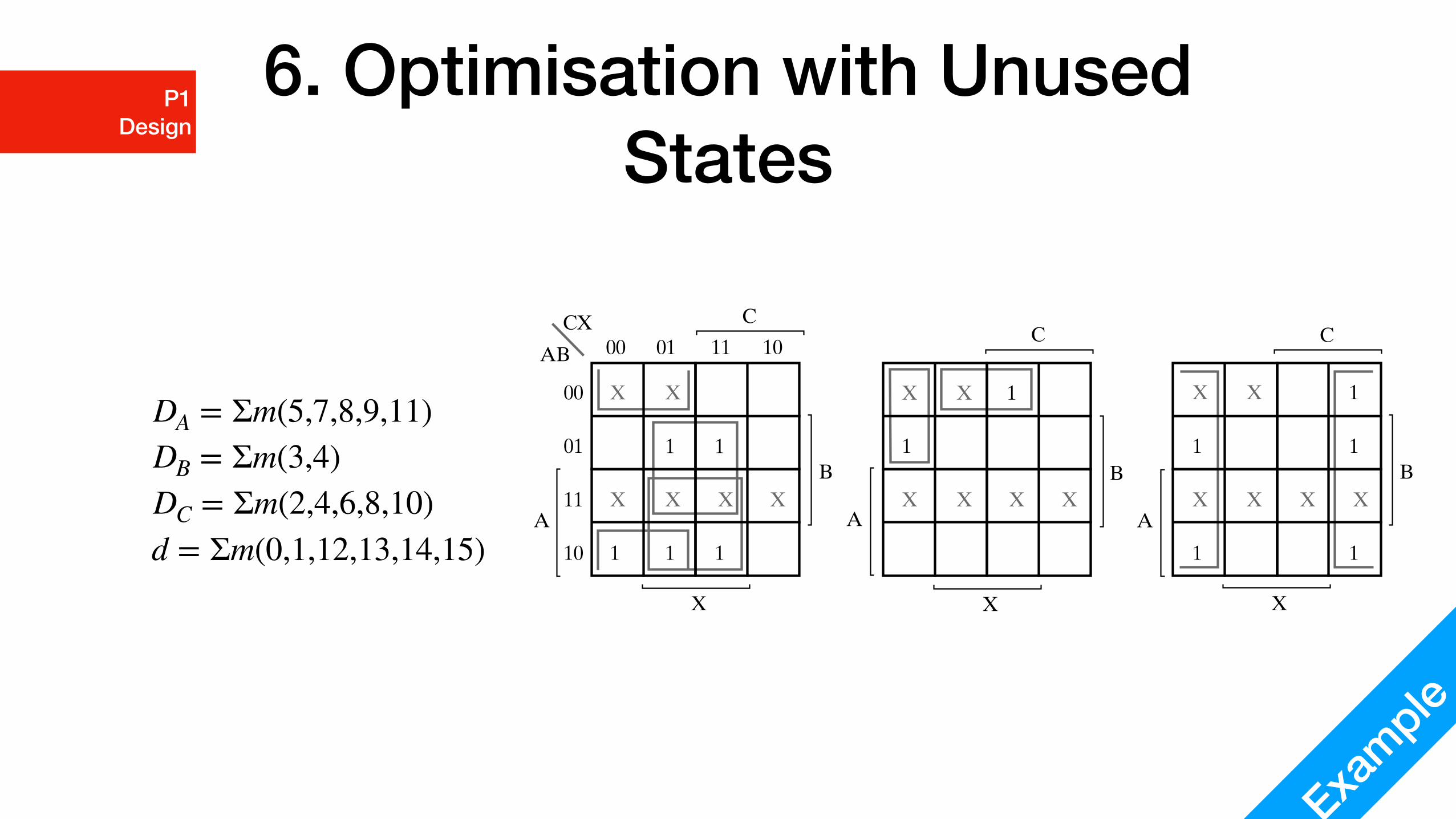
DA = Σm(5,7,8,9,11)DB = Σm(3,4)DC = Σm(2,4,6,8,10)d = Σm(0,1,12,13,14,15)

6. Optimisation with Unused States
Example
P1 Design
DA = Σm(5,7,8,9,11)DB = Σm(3,4)DC = Σm(2,4,6,8,10)d = Σm(0,1,12,13,14,15)
6. Optimisation with Unused States
Example
P1 Design
DA = Σm(5,7,8,9,11)DB = Σm(3,4)DC = Σm(2,4,6,8,10)d = Σm(0,1,12,13,14,15)
SEQUENTIAL CIRCUITS
and input columns: 0000, 0001, 1100, 1101, 1110, and 1111. These six combinationsare not listed in the state table and hence may be treated as don’t-care minterms.
The three input equations for the D flip-flops are derived from the next-statevalues and are simplified in the maps of Figure 25. Each map has six don’t-careminterms in the squares corresponding to binary 0, 1, 12, 13, 14, and 15. The opti-mized equations are
!
!
!
The logic diagram can be obtained directly from the input equations and will notbe drawn here.
It is possible that outside interference or a malfunction will cause the circuitto enter one of the unused states. Thus, it is sometimes desirable to specify, fullyor at least partially, the next-state values or the output values for the unusedstates. Depending on the function and application of the circuit, a number ofideas may be applied. First, the outputs for the unused states may be specified sothat any actions that result from entry into and transitions between the unusedstates are not harmful. Second, an additional output may be provided or anunused output code employed which indicates that the circuit has entered anincorrect state. Third, to ensure that a return to normal operation is possible with-out resetting the entire system, the next-state behavior for the unused states maybe specified. Typically, next states are selected such that one of the normally occur-ring states is reached within a few clock cycles, regardless of the input values. Thedecision as to which of the three options to apply, either individually or in combi-nation, is based on the application of the circuit or the policies of a particulardesign group.
DA AX BX B C" "
DB A C X A BX"
DC X
00
01
00 01CX
AB 11 10
11
10
X
C
X
A
B
X
1 1
X XX X
1 11
XX
1
1
X XX X
C
X
A
B
XX
1
X XX X
1
1
1
1
C
X
A
B
FIGURE 25Maps for Optimizing Input Equations
���
Systematic Design Procedures Sequential Circuits
1. Specification
2. Formulatione.g. using state table or state diagram
3. State Assignment: assign binary codes to states
4. Flip-Flop Input Equation Determination: Select flip-flop types, derive input equations from next-state entries
5. Output Equation Determination: Derive output equations from the output entries
6. Optimisation
7. Technology Mapping
8. Verification
Concep
t
P1 Design
Systematic Design ProceduresSequential Circuits
Specification
Formulation
Optimisation
Technology Mapping
Verification
Summary
3. State Assignment: assign binary codes to states
4. Flip-Flop Input Equation Determination: Select flip-flop types, derive input equations from next-state entries
5. Output Equation Determination: Derive output equations from the output entries
6. Optimisation with unused states
Review
P1 Design

Some Other Flip-Flop Types
Summary
P2 Other Flip-Flop
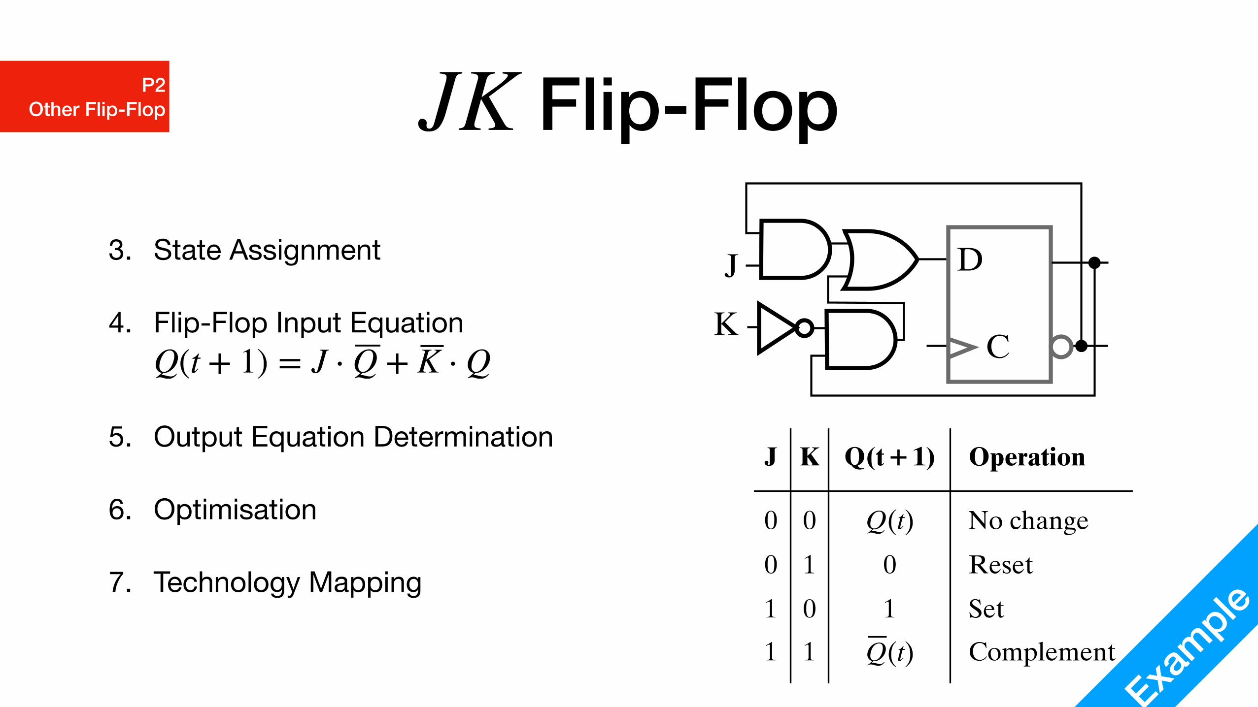
Flip-Flop; Flip-FlopJK T
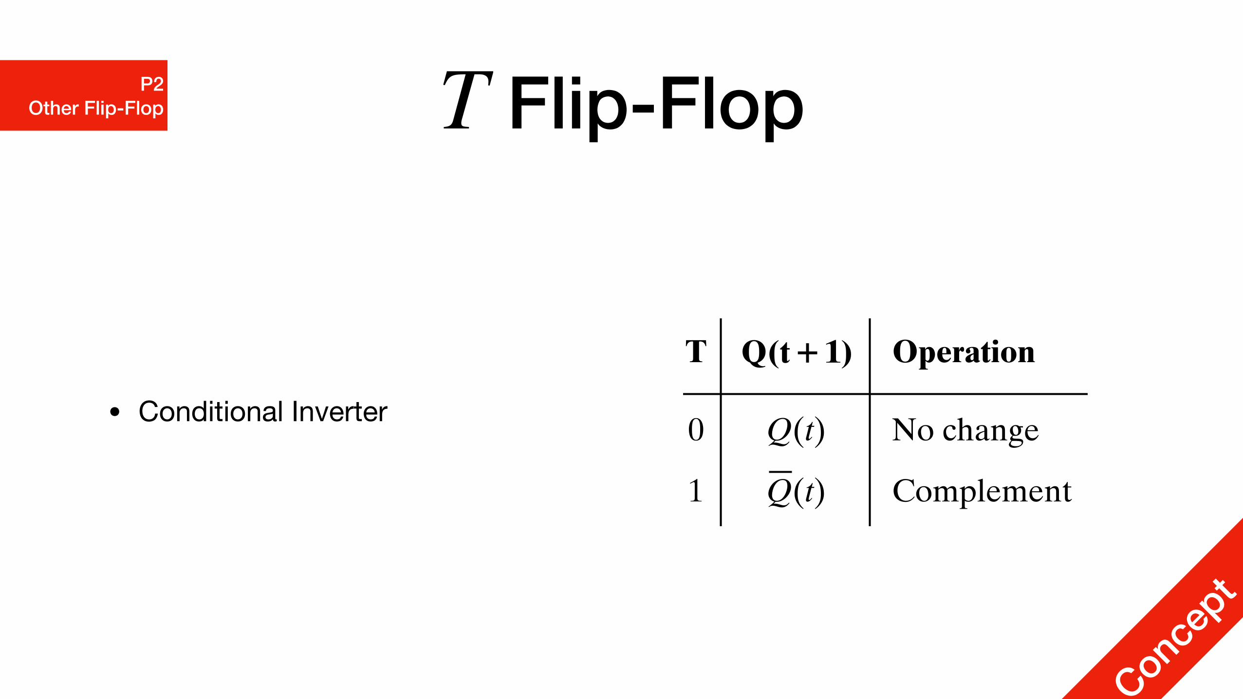
Flip-FlopT
• Conditional Inverter
Concep
t
P2 Other Flip-Flop
SEQU
ENT
IAL C
IRC
UIT
S
Characteristic Table Characteristic Equation Excitation TableType
D
SR
JK
T
D
01
Operation
0
0
1
1
0
0
1
1
ResetSet
OperationS
0
1
0
1
R
No change
Reset
Set
Undefined
01
01
D Operation
Operation
ResetSet
Q(t)
No change
Set
Reset
No change
S
X
0
1
0
0
1
1
0
0
1
1
0
Q(t)
0
0
1
1
1
0
T
Q(t)
0
0
1
1
Operation
R
X
0
X
X
0
1
1
0
K
0
1
X
X
J
No change
Set
Reset
No change
No change
No change
Set
Reset
Complement
Complement
No change
Complement
OperationOperation
OperationJ
0
1
0
1
K
0
1
T
Symbol Logic Diagrams
See Figure 6-13
See Figure 6-10
C
DT
D
CK
J
0
1
0
1
?
Q(t)
Q(t)
Q(t)
Q(t)
Q(t)
01
D
C
Q(t)
SCR
JC
K
T
C
TABLE 8Flip-Flop Logic, Characteristic Tables and Equations, and Excitation Tables
���

Flip-FlopT
• Follow 8 step design principles
• Write down the boolean expression
• Draw the circuit diagram
Example
P2 Other Flip-Flop
SEQU
ENT
IAL C
IRC
UIT
S
Characteristic Table Characteristic Equation Excitation TableType
D
SR
JK
T
D
01
Operation
0
0
1
1
0
0
1
1
ResetSet
OperationS
0
1
0
1
R
No change
Reset
Set
Undefined
01
01
D Operation
Operation
ResetSet
Q(t)
No change
Set
Reset
No change
S
X
0
1
0
0
1
1
0
0
1
1
0
Q(t)
0
0
1
1
1
0
T
Q(t)
0
0
1
1
Operation
R
X
0
X
X
0
1
1
0
K
0
1
X
X
J
No change
Set
Reset
No change
No change
No change
Set
Reset
Complement
Complement
No change
Complement
OperationOperation
OperationJ
0
1
0
1
K
0
1
T
Symbol Logic Diagrams
See Figure 6-13
See Figure 6-10
C
DT
D
CK
J
0
1
0
1
?
Q(t)
Q(t)
Q(t)
Q(t)
Q(t)
01
D
C
Q(t)
SCR
JC
K
T
C
TABLE 8Flip-Flop Logic, Characteristic Tables and Equations, and Excitation Tables
���
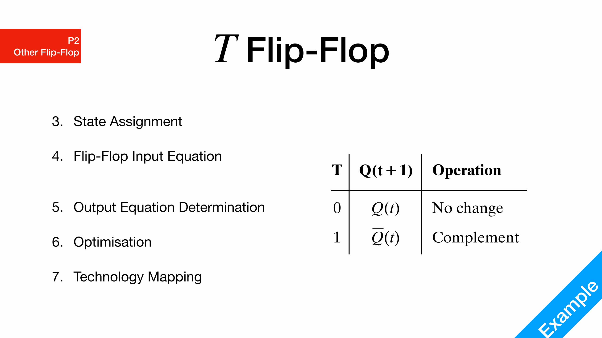
Flip-FlopT3. State Assignment
4. Flip-Flop Input Equation
5. Output Equation Determination
6. Optimisation
7. Technology Mapping
Example
P2 Other Flip-Flop
SEQU
ENT
IAL C
IRC
UIT
S
Characteristic Table Characteristic Equation Excitation TableType
D
SR
JK
T
D
01
Operation
0
0
1
1
0
0
1
1
ResetSet
OperationS
0
1
0
1
R
No change
Reset
Set
Undefined
01
01
D Operation
Operation
ResetSet
Q(t)
No change
Set
Reset
No change
S
X
0
1
0
0
1
1
0
0
1
1
0
Q(t)
0
0
1
1
1
0
T
Q(t)
0
0
1
1
Operation
R
X
0
X
X
0
1
1
0
K
0
1
X
X
J
No change
Set
Reset
No change
No change
No change
Set
Reset
Complement
Complement
No change
Complement
OperationOperation
OperationJ
0
1
0
1
K
0
1
T
Symbol Logic Diagrams
See Figure 6-13
See Figure 6-10
C
DT
D
CK
J
0
1
0
1
?
Q(t)
Q(t)
Q(t)
Q(t)
Q(t)
01
D
C
Q(t)
SCR
JC
K
T
C
TABLE 8Flip-Flop Logic, Characteristic Tables and Equations, and Excitation Tables
���
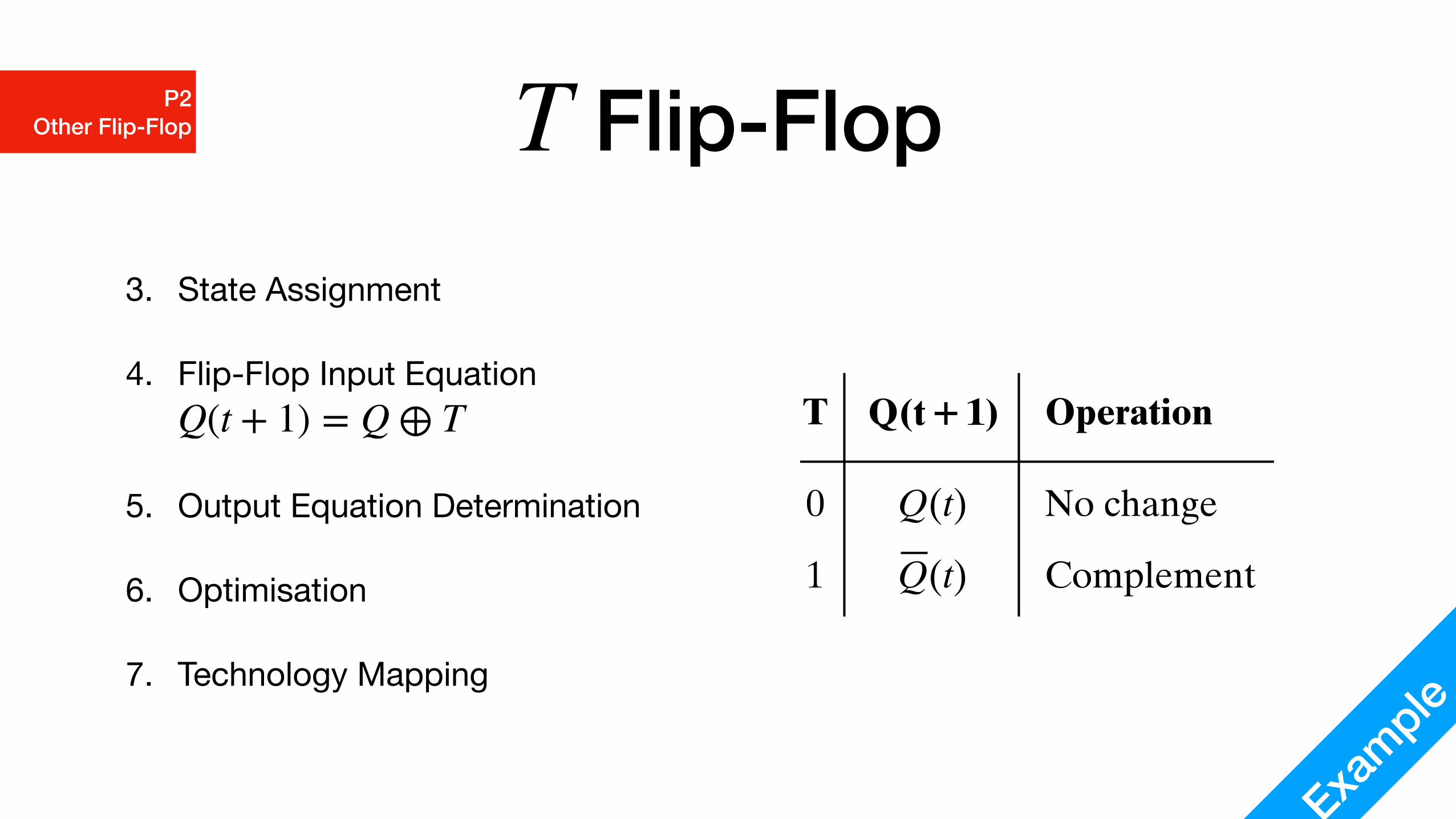
Flip-FlopT3. State Assignment
4. Flip-Flop Input Equation
5. Output Equation Determination
6. Optimisation
7. Technology Mapping
Q(t + 1) = Q ⊕ T
Example
P2 Other Flip-Flop
SEQU
ENT
IAL C
IRC
UIT
S
Characteristic Table Characteristic Equation Excitation TableType
D
SR
JK
T
D
01
Operation
0
0
1
1
0
0
1
1
ResetSet
OperationS
0
1
0
1
R
No change
Reset
Set
Undefined
01
01
D Operation
Operation
ResetSet
Q(t)
No change
Set
Reset
No change
S
X
0
1
0
0
1
1
0
0
1
1
0
Q(t)
0
0
1
1
1
0
T
Q(t)
0
0
1
1
Operation
R
X
0
X
X
0
1
1
0
K
0
1
X
X
J
No change
Set
Reset
No change
No change
No change
Set
Reset
Complement
Complement
No change
Complement
OperationOperation
OperationJ
0
1
0
1
K
0
1
T
Symbol Logic Diagrams
See Figure 6-13
See Figure 6-10
C
DT
D
CK
J
0
1
0
1
?
Q(t)
Q(t)
Q(t)
Q(t)
Q(t)
01
D
C
Q(t)
SCR
JC
K
T
C
TABLE 8Flip-Flop Logic, Characteristic Tables and Equations, and Excitation Tables
���
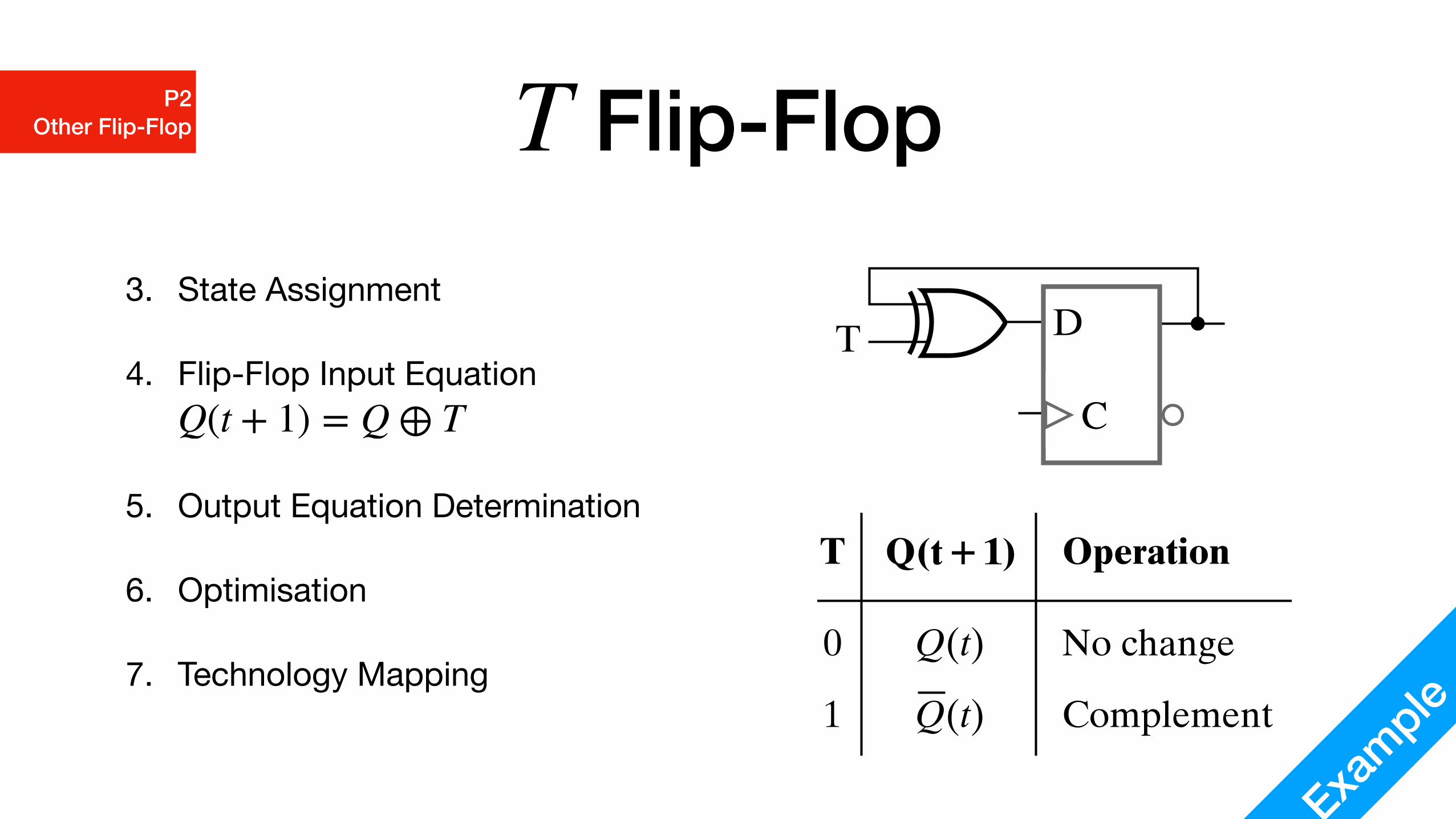
Flip-FlopT3. State Assignment
4. Flip-Flop Input Equation
5. Output Equation Determination
6. Optimisation
7. Technology Mapping
Q(t + 1) = Q ⊕ T
P2 Other Flip-Flop
Example
SEQU
ENT
IAL C
IRC
UIT
S
Characteristic Table Characteristic Equation Excitation TableType
D
SR
JK
T
D
01
Operation
0
0
1
1
0
0
1
1
ResetSet
OperationS
0
1
0
1
R
No change
Reset
Set
Undefined
01
01
D Operation
Operation
ResetSet
Q(t)
No change
Set
Reset
No change
S
X
0
1
0
0
1
1
0
0
1
1
0
Q(t)
0
0
1
1
1
0
T
Q(t)
0
0
1
1
Operation
R
X
0
X
X
0
1
1
0
K
0
1
X
X
J
No change
Set
Reset
No change
No change
No change
Set
Reset
Complement
Complement
No change
Complement
OperationOperation
OperationJ
0
1
0
1
K
0
1
T
Symbol Logic Diagrams
See Figure 6-13
See Figure 6-10
C
DT
D
CK
J
0
1
0
1
?
Q(t)
Q(t)
Q(t)
Q(t)
Q(t)
01
D
C
Q(t)
SCR
JC
K
T
C
TABLE 8Flip-Flop Logic, Characteristic Tables and Equations, and Excitation Tables
���
C
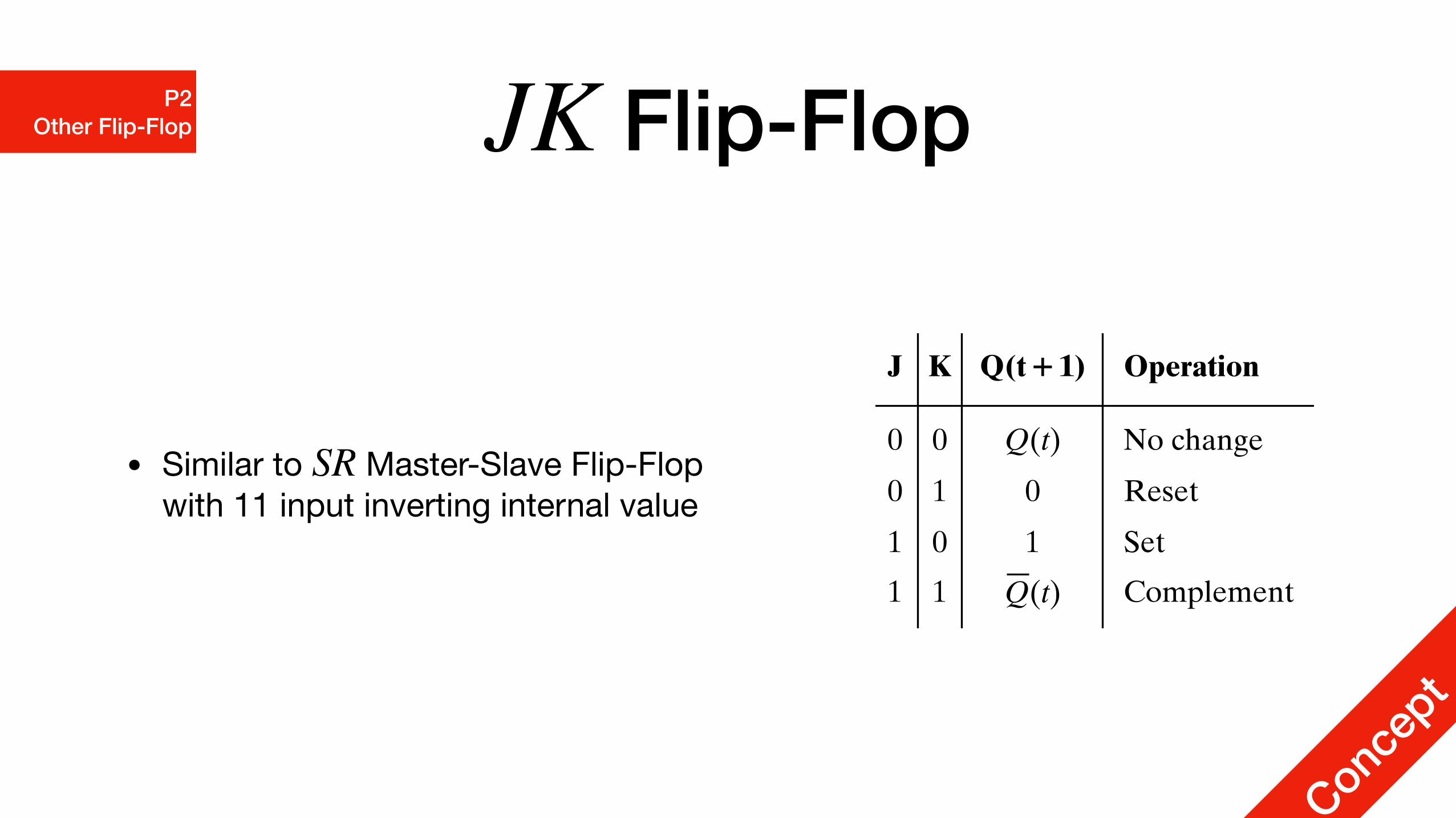
Flip-FlopJK
• Similar to Master-Slave Flip-Flopwith 11 input inverting internal value
SR
Concep
t
P2 Other Flip-Flop
SEQU
ENT
IAL C
IRC
UIT
S
Characteristic Table Characteristic Equation Excitation TableType
D
SR
JK
T
D
01
Operation
0
0
1
1
0
0
1
1
ResetSet
OperationS
0
1
0
1
R
No change
Reset
Set
Undefined
01
01
D Operation
Operation
ResetSet
Q(t)
No change
Set
Reset
No change
S
X
0
1
0
0
1
1
0
0
1
1
0
Q(t)
0
0
1
1
1
0
T
Q(t)
0
0
1
1
Operation
R
X
0
X
X
0
1
1
0
K
0
1
X
X
J
No change
Set
Reset
No change
No change
No change
Set
Reset
Complement
Complement
No change
Complement
OperationOperation
OperationJ
0
1
0
1
K
0
1
T
Symbol Logic Diagrams
See Figure 6-13
See Figure 6-10
C
DT
D
CK
J
0
1
0
1
?
Q(t)
Q(t)
Q(t)
Q(t)
Q(t)
01
D
C
Q(t)
SCR
JC
K
T
C
TABLE 8Flip-Flop Logic, Characteristic Tables and Equations, and Excitation Tables
���
Flip-FlopJK
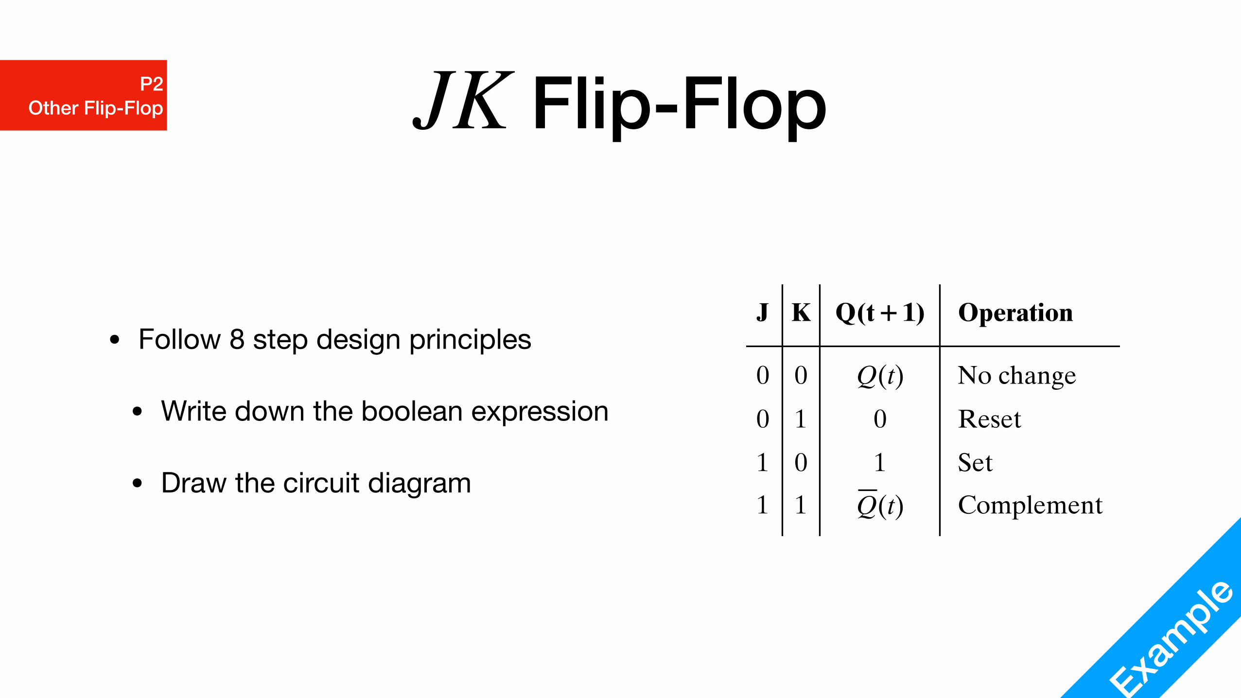
• Follow 8 step design principles
• Write down the boolean expression
• Draw the circuit diagram
Example
P2 Other Flip-Flop
SEQU
ENT
IAL C
IRC
UIT
S
Characteristic Table Characteristic Equation Excitation TableType
D
SR
JK
T
D
01
Operation
0
0
1
1
0
0
1
1
ResetSet
OperationS
0
1
0
1
R
No change
Reset
Set
Undefined
01
01
D Operation
Operation
ResetSet
Q(t)
No change
Set
Reset
No change
S
X
0
1
0
0
1
1
0
0
1
1
0
Q(t)
0
0
1
1
1
0
T
Q(t)
0
0
1
1
Operation
R
X
0
X
X
0
1
1
0
K
0
1
X
X
J
No change
Set
Reset
No change
No change
No change
Set
Reset
Complement
Complement
No change
Complement
OperationOperation
OperationJ
0
1
0
1
K
0
1
T
Symbol Logic Diagrams
See Figure 6-13
See Figure 6-10
C
DT
D
CK
J
0
1
0
1
?
Q(t)
Q(t)
Q(t)
Q(t)
Q(t)
01
D
C
Q(t)
SCR
JC
K
T
C
TABLE 8Flip-Flop Logic, Characteristic Tables and Equations, and Excitation Tables
���
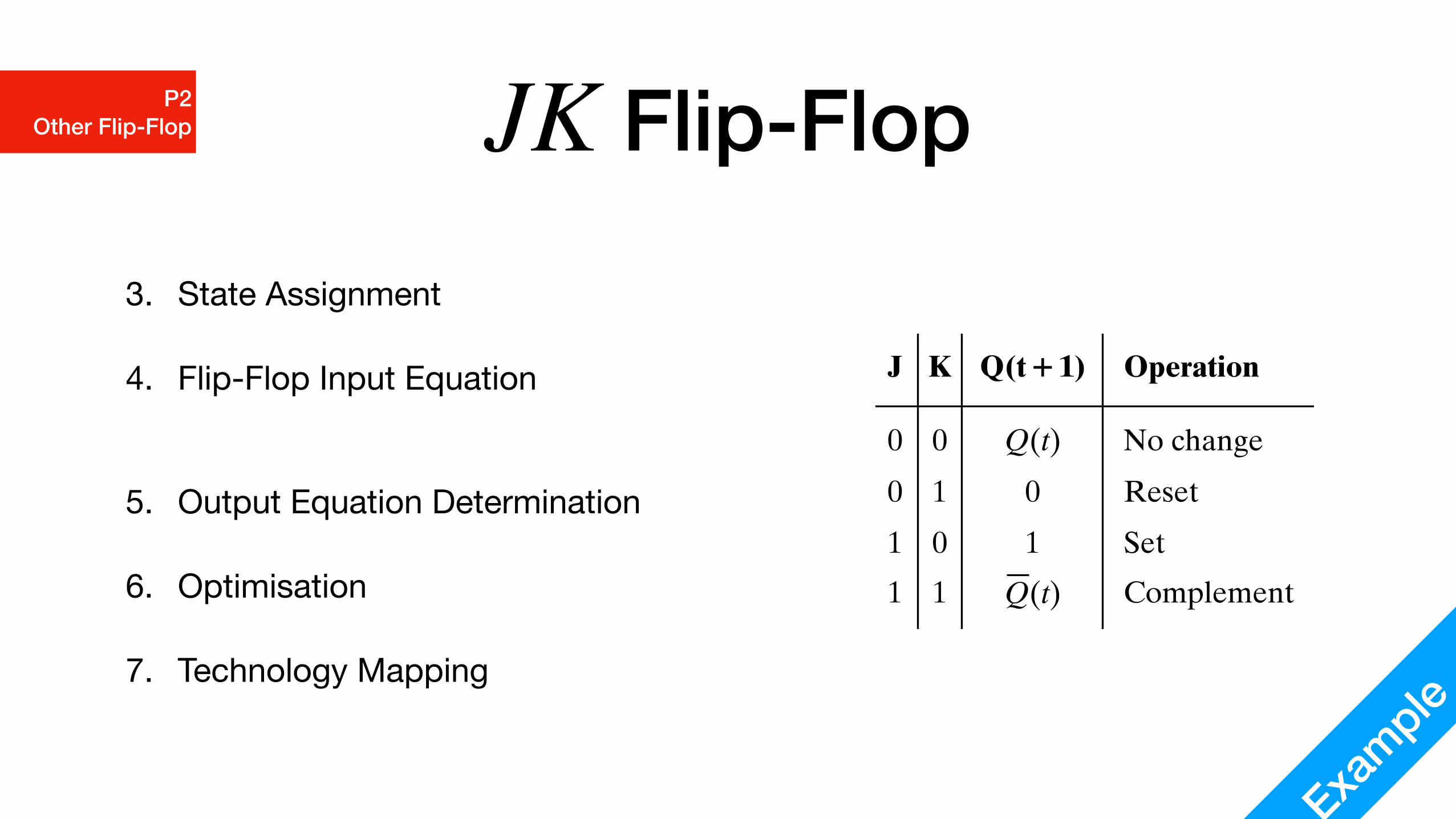
Flip-FlopJK3. State Assignment
4. Flip-Flop Input Equation
5. Output Equation Determination
6. Optimisation
7. Technology Mapping
Example
P2 Other Flip-Flop
SEQU
ENT
IAL C
IRC
UIT
S
Characteristic Table Characteristic Equation Excitation TableType
D
SR
JK
T
D
01
Operation
0
0
1
1
0
0
1
1
ResetSet
OperationS
0
1
0
1
R
No change
Reset
Set
Undefined
01
01
D Operation
Operation
ResetSet
Q(t)
No change
Set
Reset
No change
S
X
0
1
0
0
1
1
0
0
1
1
0
Q(t)
0
0
1
1
1
0
T
Q(t)
0
0
1
1
Operation
R
X
0
X
X
0
1
1
0
K
0
1
X
X
J
No change
Set
Reset
No change
No change
No change
Set
Reset
Complement
Complement
No change
Complement
OperationOperation
OperationJ
0
1
0
1
K
0
1
T
Symbol Logic Diagrams
See Figure 6-13
See Figure 6-10
C
DT
D
CK
J
0
1
0
1
?
Q(t)
Q(t)
Q(t)
Q(t)
Q(t)
01
D
C
Q(t)
SCR
JC
K
T
C
TABLE 8Flip-Flop Logic, Characteristic Tables and Equations, and Excitation Tables
���
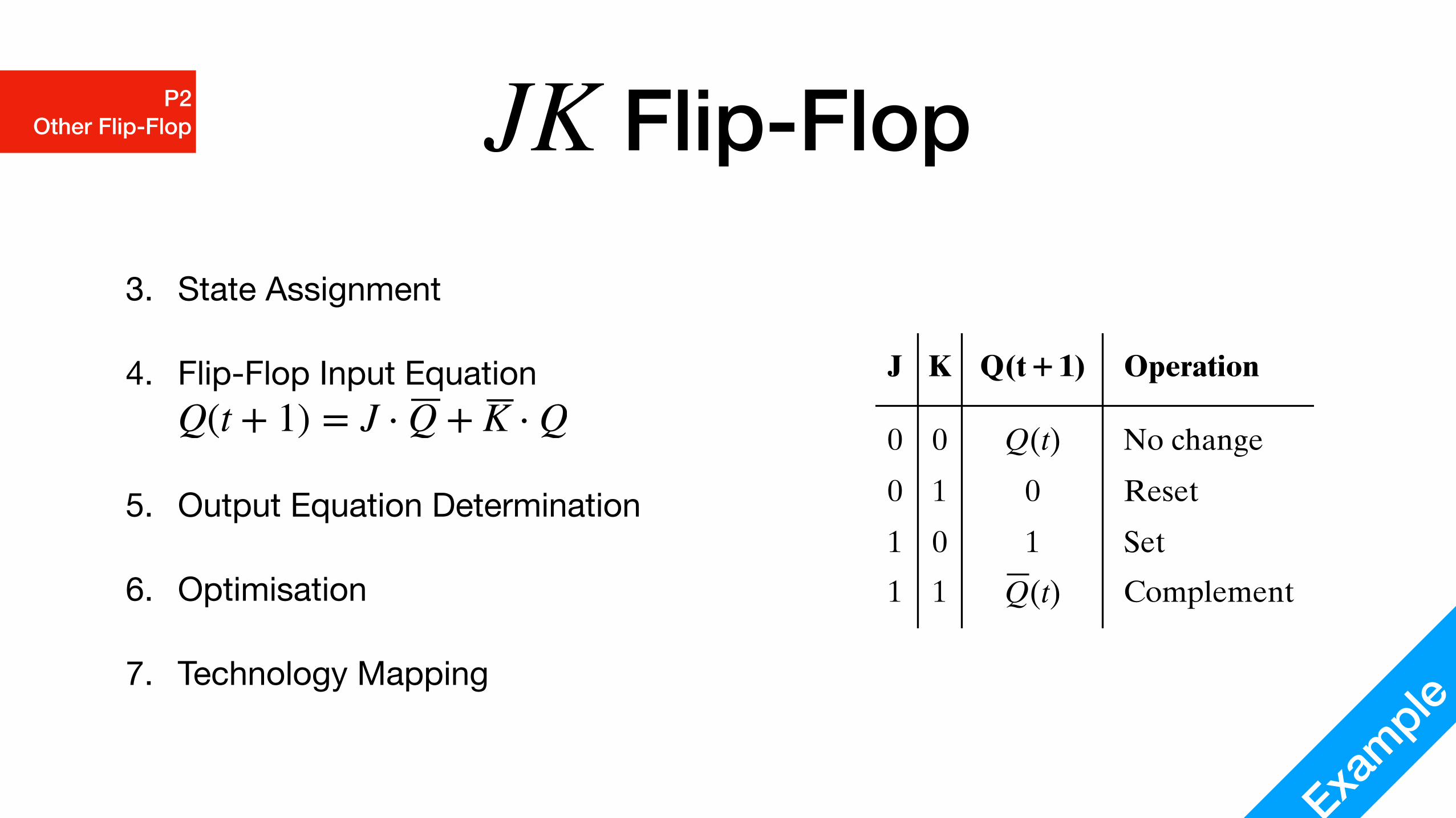
Flip-FlopJK3. State Assignment
4. Flip-Flop Input Equation
5. Output Equation Determination
6. Optimisation
7. Technology Mapping
Q(t + 1) = J ⋅ Q + K ⋅ Q
Example
P2 Other Flip-Flop
SEQU
ENT
IAL C
IRC
UIT
S
Characteristic Table Characteristic Equation Excitation TableType
D
SR
JK
T
D
01
Operation
0
0
1
1
0
0
1
1
ResetSet
OperationS
0
1
0
1
R
No change
Reset
Set
Undefined
01
01
D Operation
Operation
ResetSet
Q(t)
No change
Set
Reset
No change
S
X
0
1
0
0
1
1
0
0
1
1
0
Q(t)
0
0
1
1
1
0
T
Q(t)
0
0
1
1
Operation
R
X
0
X
X
0
1
1
0
K
0
1
X
X
J
No change
Set
Reset
No change
No change
No change
Set
Reset
Complement
Complement
No change
Complement
OperationOperation
OperationJ
0
1
0
1
K
0
1
T
Symbol Logic Diagrams
See Figure 6-13
See Figure 6-10
C
DT
D
CK
J
0
1
0
1
?
Q(t)
Q(t)
Q(t)
Q(t)
Q(t)
01
D
C
Q(t)
SCR
JC
K
T
C
TABLE 8Flip-Flop Logic, Characteristic Tables and Equations, and Excitation Tables
���
Flip-FlopJK3. State Assignment
4. Flip-Flop Input Equation
5. Output Equation Determination
6. Optimisation
7. Technology Mapping
Q(t + 1) = J ⋅ Q + K ⋅ Q
P2 Other Flip-Flop
SEQU
ENT
IAL C
IRC
UIT
S
Characteristic Table Characteristic Equation Excitation TableType
D
SR
JK
T
D
01
Operation
0
0
1
1
0
0
1
1
ResetSet
OperationS
0
1
0
1
R
No change
Reset
Set
Undefined
01
01
D Operation
Operation
ResetSet
Q(t)
No change
Set
Reset
No change
S
X
0
1
0
0
1
1
0
0
1
1
0
Q(t)
0
0
1
1
1
0
T
Q(t)
0
0
1
1
Operation
R
X
0
X
X
0
1
1
0
K
0
1
X
X
J
No change
Set
Reset
No change
No change
No change
Set
Reset
Complement
Complement
No change
Complement
OperationOperation
OperationJ
0
1
0
1
K
0
1
T
Symbol Logic Diagrams
See Figure 6-13
See Figure 6-10
C
DT
D
CK
J
0
1
0
1
?
Q(t)
Q(t)
Q(t)
Q(t)
Q(t)
01
D
C
Q(t)
SCR
JC
K
T
C
TABLE 8Flip-Flop Logic, Characteristic Tables and Equations, and Excitation Tables
���
Example
SEQU
ENT
IAL C
IRC
UIT
S
Characteristic Table Characteristic Equation Excitation TableType
D
SR
JK
T
D
01
Operation
0
0
1
1
0
0
1
1
ResetSet
OperationS
0
1
0
1
R
No change
Reset
Set
Undefined
01
01
D Operation
Operation
ResetSet
Q(t)
No change
Set
Reset
No change
S
X
0
1
0
0
1
1
0
0
1
1
0
Q(t)
0
0
1
1
1
0
T
Q(t)
0
0
1
1
Operation
R
X
0
X
X
0
1
1
0
K
0
1
X
X
J
No change
Set
Reset
No change
No change
No change
Set
Reset
Complement
Complement
No change
Complement
OperationOperation
OperationJ
0
1
0
1
K
0
1
T
Symbol Logic Diagrams
See Figure 6-13
See Figure 6-10
C
DT
D
CK
J
0
1
0
1
?
Q(t)
Q(t)
Q(t)
Q(t)
Q(t)
01
D
C
Q(t)
SCR
JC
K
T
C
TABLE 8Flip-Flop Logic, Characteristic Tables and Equations, and Excitation Tables
���
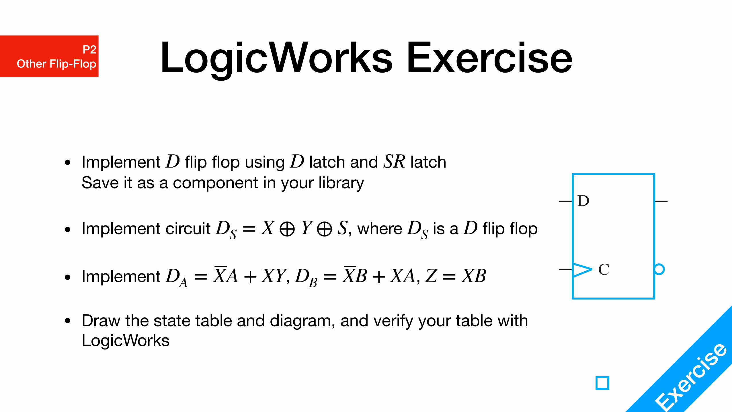
LogicWorks Exercise
Exerci
se
P2 Other Flip-Flop
YX Z• Implement flip flop using latch and latch
Save it as a component in your library
• Implement circuit , where is a flip flop
• Implement , ,
• Draw the state table and diagram, and verify your table with LogicWorks
D D SR
DS = X ⊕ Y ⊕ S DS D
DA = XA + XY DB = XB + XA Z = XB
4-3 / Flip-Flops 207
When the positive edge occurs, the clock input changes to 1. This disables the master latch so that its value is !xed and enables the slave latch so that it copies the state of the master latch. The state of the master latch to be copied is the state that is present at the positive edge of the clock. Thus, the behavior appears to be edge triggered. With the clock input equal to 1, the master latch is disabled and cannot change, so the state of both the master and the slave remain unchanged. Finally, when the clock input changes from 1 to 0, the master is enabled and begins following the D value. But during the 1- to- 0 transition, the slave is disabled before any change in the master can reach it. Thus, the value stored in the slave remains unchanged during this transition. An alternative implementation that requires fewer gates is given in Problem 4-3 at the end of the chapter.
Standard Graphics Symbols
The standard graphics symbols for the different types of latches and "ip- "ops are shown in Figure 4-11. A "ip- "op or latch is designated by a rectangular block with
(a) Latches
S
R
SR SR
S
R
D with 0 Control
D
C
D with 1 Control
D
C
(b) Master–slave flip-flops
D
C
Triggered DTriggered SR
S
R
C
D
C
Triggered DTriggered SR
S
R
C
(c) Edge-triggered flip-flops
Triggered D
D
C
Triggered D
D
C
FIGURE 4-11Standard Graphics Symbols for Latches and Flip- Flop
M04_MANO0637_05_SE_C04.indd 207 23/01/15 1:54 PM

Implementation
• Implement Flip-Flop
• Is there any other way to implement? What if you cannot use Flip-Flop?
• Implement Flip-Flop
JK
D
T
Tech
nical
P2 Other Flip-Flop
Related Documents