January 2006 1 Verilog Digital System Desi gn Copyright Z. Navabi, 2006 Verilog Digital System Design Verilog Digital System Design Z. Navabi, McGraw-Hill, 2005 Z. Navabi, McGraw-Hill, 2005 Chapter 1 Chapter 1 Digital System Design Digital System Design Automation with Verilog Automation with Verilog Prepared by: Prepared by: Homa Alemzadeh Homa Alemzadeh

0071445641_Chapter_1
Oct 21, 2015
Manual Verlog
Welcome message from author
This document is posted to help you gain knowledge. Please leave a comment to let me know what you think about it! Share it to your friends and learn new things together.
Transcript
January 2006 1Verilog Digital System Design Copyright Z. Navabi, 2006
Verilog Digital System Design Verilog Digital System Design Z. Navabi, McGraw-Hill, 2005Z. Navabi, McGraw-Hill, 2005
Chapter 1Chapter 1Digital System DesignDigital System Design
Automation with VerilogAutomation with Verilog
Prepared by:Prepared by:Homa AlemzadehHoma Alemzadeh
January 2006 2Verilog Digital System Design Copyright Z. Navabi, 2006
Digital System DesignDigital System DesignAutomation with VerilogAutomation with Verilog
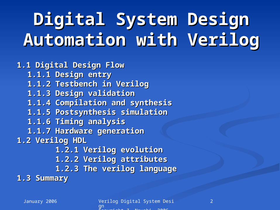
1.1 Digital Design Flow1.1 Digital Design Flow1.1.1 Design entry1.1.1 Design entry1.1.2 Testbench in Verilog1.1.2 Testbench in Verilog 1.1.3 Design validation1.1.3 Design validation 1.1.4 Compilation and synthesis1.1.4 Compilation and synthesis 1.1.5 Postsynthesis simulation1.1.5 Postsynthesis simulation 1.1.6 Timing analysis1.1.6 Timing analysis 1.1.7 Hardware generation1.1.7 Hardware generation
1.2 Verilog HDL1.2 Verilog HDL 1.2.1 Verilog evolution1.2.1 Verilog evolution 1.2.2 Verilog attributes1.2.2 Verilog attributes 1.2.3 The verilog language1.2.3 The verilog language
1.3 Summary1.3 Summary
January 2006 3Verilog Digital System Design Copyright Z. Navabi, 2006
Digital System DesignDigital System DesignAutomation with VerilogAutomation with Verilog
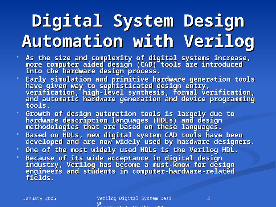
As the size and complexity of digital systems increase, As the size and complexity of digital systems increase, more computer aided design (CAD) tools are introduced more computer aided design (CAD) tools are introduced into the hardware design process. into the hardware design process.
Early simulation and primitive hardware generation Early simulation and primitive hardware generation tools have given way to sophisticated design entry, tools have given way to sophisticated design entry, verification, high-level synthesis, formal verification, and verification, high-level synthesis, formal verification, and automatic hardware generation and device programming automatic hardware generation and device programming tools. tools.
Growth of design automation tools is largely due to Growth of design automation tools is largely due to hardware description languages (HDLs) and design hardware description languages (HDLs) and design methodologies that are based on these languages. methodologies that are based on these languages.
Based on HDLs, new digital system CAD tools have been Based on HDLs, new digital system CAD tools have been developed and are now widely used by hardware developed and are now widely used by hardware designers. designers.
One of the most widely used HDLs is the Verilog HDL. One of the most widely used HDLs is the Verilog HDL. Because of its wide acceptance in digital design industry, Because of its wide acceptance in digital design industry,
Verilog has become a must-know for design engineers Verilog has become a must-know for design engineers and students in computer-hardware-related fields.and students in computer-hardware-related fields.
January 2006 4Verilog Digital System Design Copyright Z. Navabi, 2006
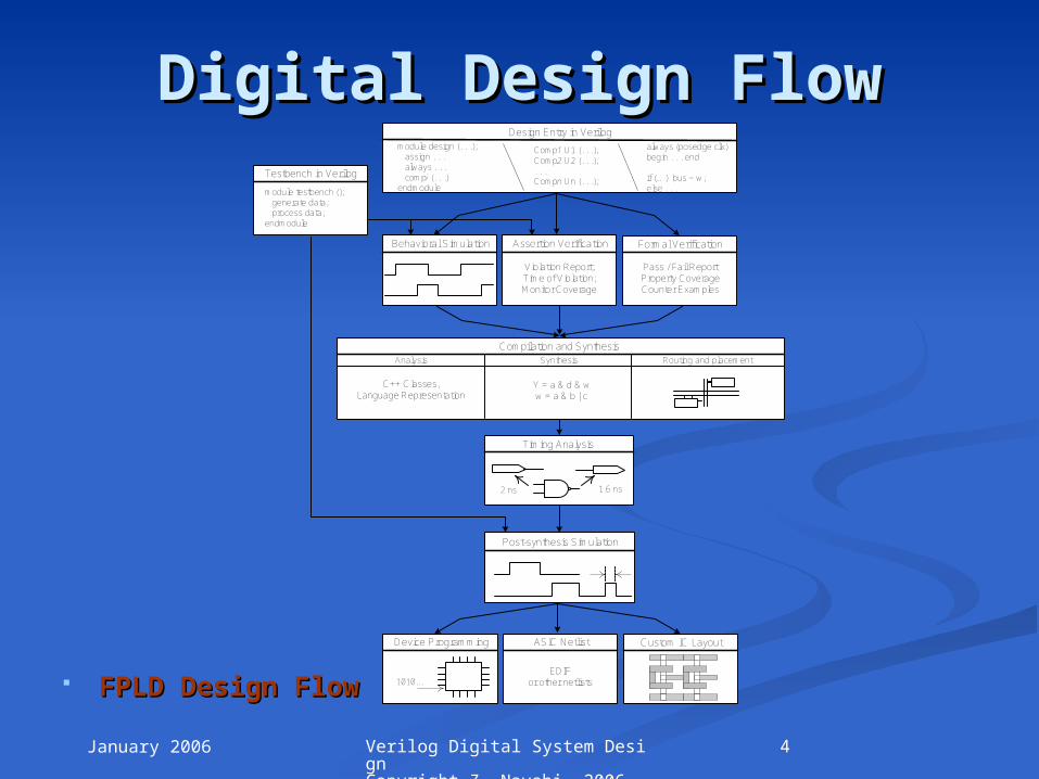
Digital Design FlowDigital Design Flow
FPLD Design FlowFPLD Design Flow
Compilation and SynthesisAnalysis Synthesis Routing and placement
Y = a & d & ww = a & b | c
Post-synthesis Simulation
Timing Analysis
1.6 ns2 ns
C++ Classes, Language Representation
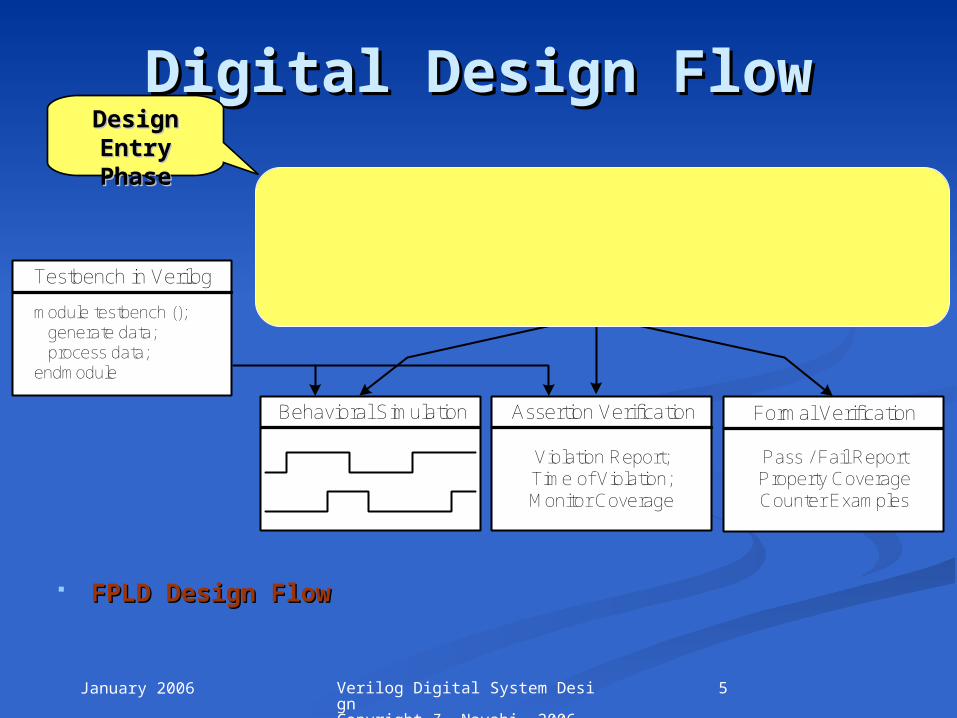
Behavioral Simulation Assertion Verification Formal Verification
Violation Report;Time of Violation;Monitor Coverage
Pass / Fail ReportProperty CoverageCounter Examples
Design Entry in Verilogalways (posedge clk) begin . . . end
if (…) bus = w;else . . .
Comp1 U1 (. . .);Comp2 U2 (. . .);. . .Compn Un (. . .);
module design (. . .); assign . . . always . . . compi (. . .)endmodule
Testbench in Verilog
module testbench (); generate data; process data;endmodule
Device Programming ASIC Netlist Custom IC Layout
EDIFor other netlists1010...
January 2006 5Verilog Digital System Design Copyright Z. Navabi, 2006
Digital Design FlowDigital Design Flow
FPLD Design FlowFPLD Design Flow
Behavioral Simulation Assertion Verification Formal Verification
Violation Report;Time of Violation;Monitor Coverage
Pass / Fail ReportProperty CoverageCounter Examples
Design Entry in Verilogalways (posedge clk) begin . . . end
if (…) bus = w;else . . .
Comp1 U1 (. . .);Comp2 U2 (. . .);. . .Compn Un (. . .);
module design (. . .); assign . . . always . . . compi (. . .)endmodule
Testbench in Verilog
module testbench (); generate data; process data;endmodule
Design Design EntryEntryPhasePhase
January 2006 6Verilog Digital System Design Copyright Z. Navabi, 2006
Digital Design FlowDigital Design Flow
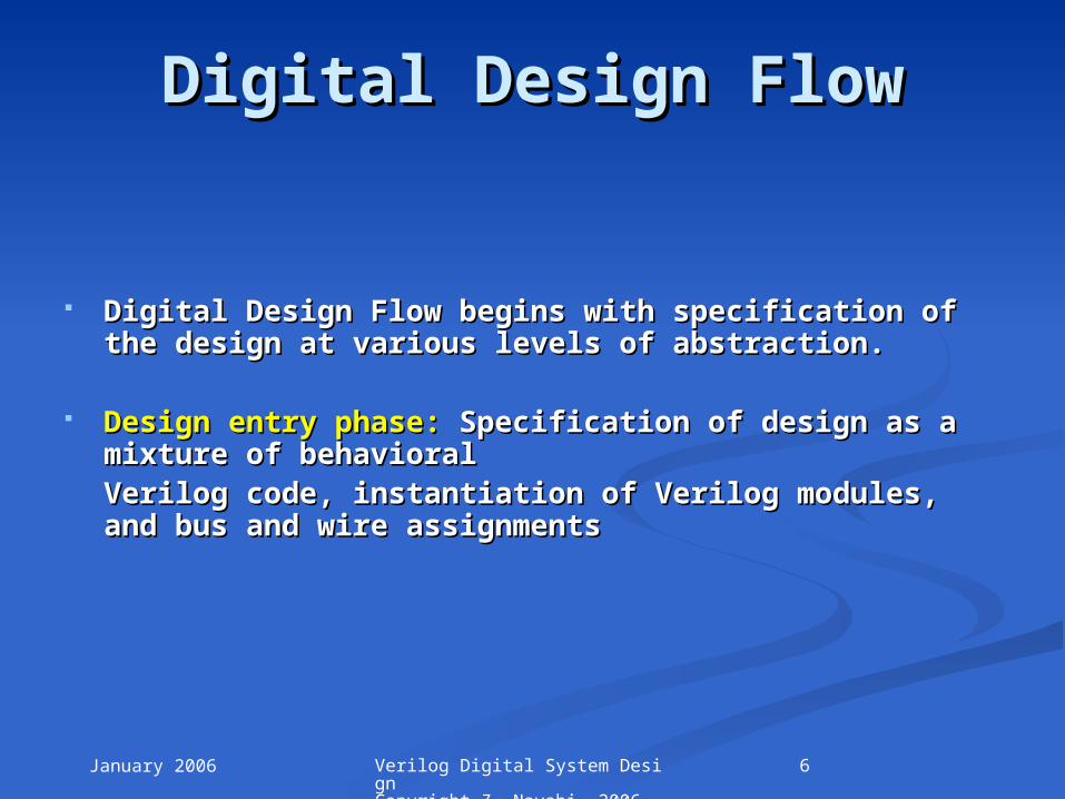
Digital Design Flow begins with specification of the Digital Design Flow begins with specification of the design at various levels of abstraction.design at various levels of abstraction.
Design entry phase:Design entry phase: Specification of design as a Specification of design as a mixture of behavioralmixture of behavioralVerilog code, instantiation of Verilog modules, and Verilog code, instantiation of Verilog modules, and bus and wire assignmentsbus and wire assignments
January 2006 7Verilog Digital System Design Copyright Z. Navabi, 2006
Compilation and SynthesisAnalysis Synthesis Routing and placement
Y = a & d & ww = a & b | c
Timing Analysis
1.6 ns2 ns
C++ Classes, Language Representation
Behavioral Simulation Assertion Verification Formal Verification
Violation Report;Time of Violation;Monitor Coverage
Pass / Fail ReportProperty CoverageCounter Examples
Digital Design FlowDigital Design Flow
FPLD Design Flow FPLD Design Flow (Continued)(Continued)
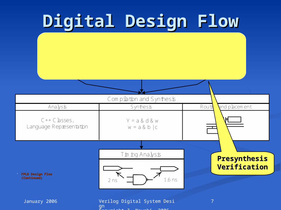
PresynthesisPresynthesisVerificationVerification
January 2006 8Verilog Digital System Design Copyright Z. Navabi, 2006
Digital Design FlowDigital Design Flow
Presynthesis verification:Presynthesis verification: Generating testbenches for Generating testbenches for verification of the design and later for verifying the verification of the design and later for verifying the synthesis outputsynthesis output
January 2006 9Verilog Digital System Design Copyright Z. Navabi, 2006
Compilation and SynthesisAnalysis Synthesis Routing and placement
Y = a & d & ww = a & b | c
Timing Analysis
1.6 ns2 ns
C++ Classes, Language Representation
Behavioral Simulation Assertion Verification Formal Verification
Violation Report;Time of Violation;Monitor Coverage
Pass / Fail ReportProperty CoverageCounter Examples
Digital Design FlowDigital Design Flow
FPLD Design Flow FPLD Design Flow (Continued)(Continued)
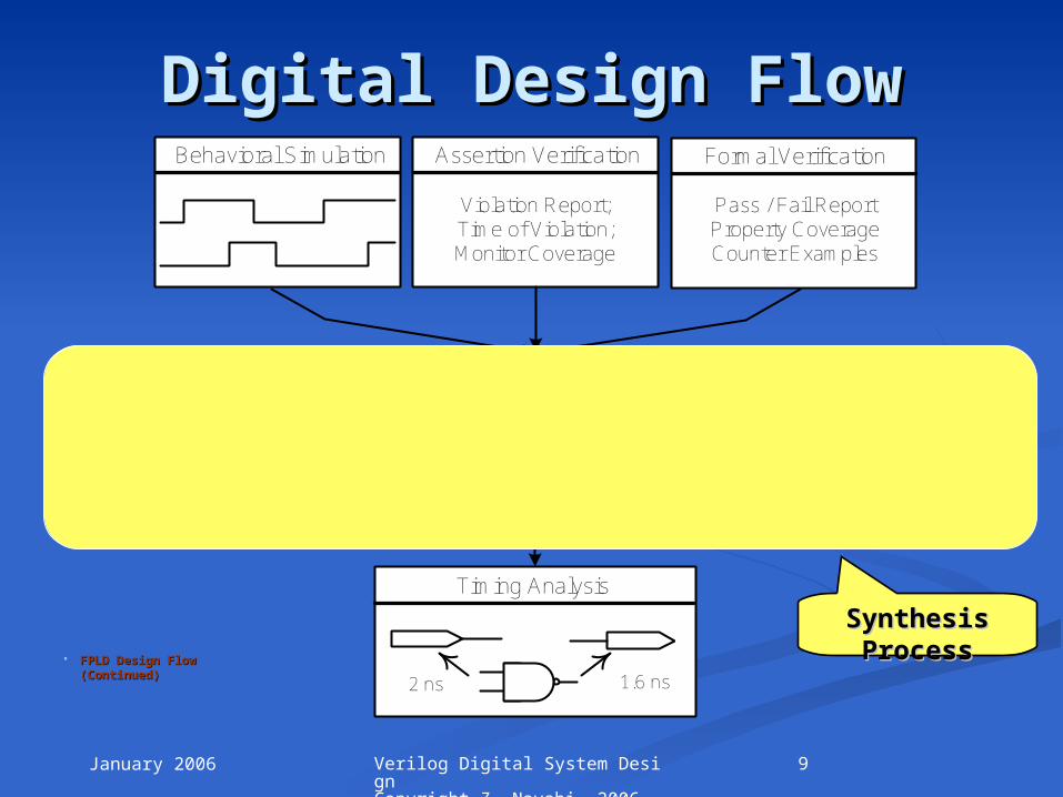
Synthesis Synthesis ProcessProcess
January 2006 10Verilog Digital System Design Copyright Z. Navabi, 2006
Digital Design FlowDigital Design Flow
Synthesis process:Synthesis process: Translating the design into actual Translating the design into actual hardware of a target device (FPLD, ASIC or custom hardware of a target device (FPLD, ASIC or custom IC)IC)
January 2006 11Verilog Digital System Design Copyright Z. Navabi, 2006
Digital Design FlowDigital Design Flow
FPLD Design Flow (Continued)FPLD Design Flow (Continued)
Post-synthesis Simulation
Timing Analysis
1.6 ns2 ns
Testbench in Verilog
module testbench (); generate data; process data;endmodule
Device Programming ASIC Netlist Custom IC Layout
EDIFor other netlists1010...
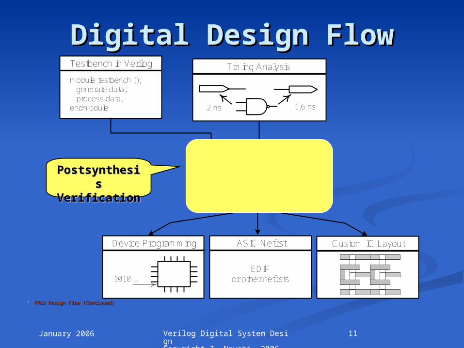
PostsynthesiPostsynthesiss
VerificationVerification
January 2006 12Verilog Digital System Design Copyright Z. Navabi, 2006
Digital Design FlowDigital Design Flow
Postsynthesis simulation:Postsynthesis simulation: Testing the behavioral Testing the behavioral model of the design and its hardware model by using model of the design and its hardware model by using presynthesis test datapresynthesis test data

January 2006 13Verilog Digital System Design Copyright Z. Navabi, 2006
Digital Design FlowDigital Design Flow
FPLD Design Flow (Continued)FPLD Design Flow (Continued)
Post-synthesis Simulation
Timing Analysis
1.6 ns2 ns
Testbench in Verilog
module testbench (); generate data; process data;endmodule
Device Programming ASIC Netlist Custom IC Layout
EDIFor other netlists1010...
January 2006 14Verilog Digital System Design Copyright Z. Navabi, 2006
Digital Design FlowDigital Design Flow
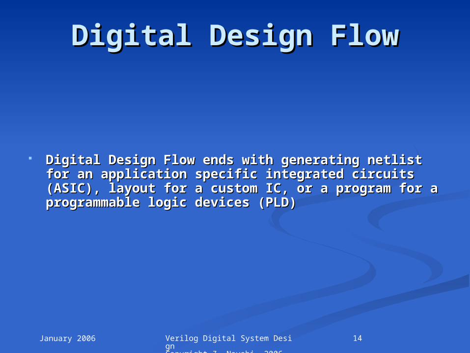
Digital Design Flow ends with generating netlist for Digital Design Flow ends with generating netlist for an application specific integrated circuits (ASIC), an application specific integrated circuits (ASIC), layout for a custom IC, or a program for a layout for a custom IC, or a program for a programmable logic devices (PLD)programmable logic devices (PLD)
January 2006 15Verilog Digital System Design Copyright Z. Navabi, 2006
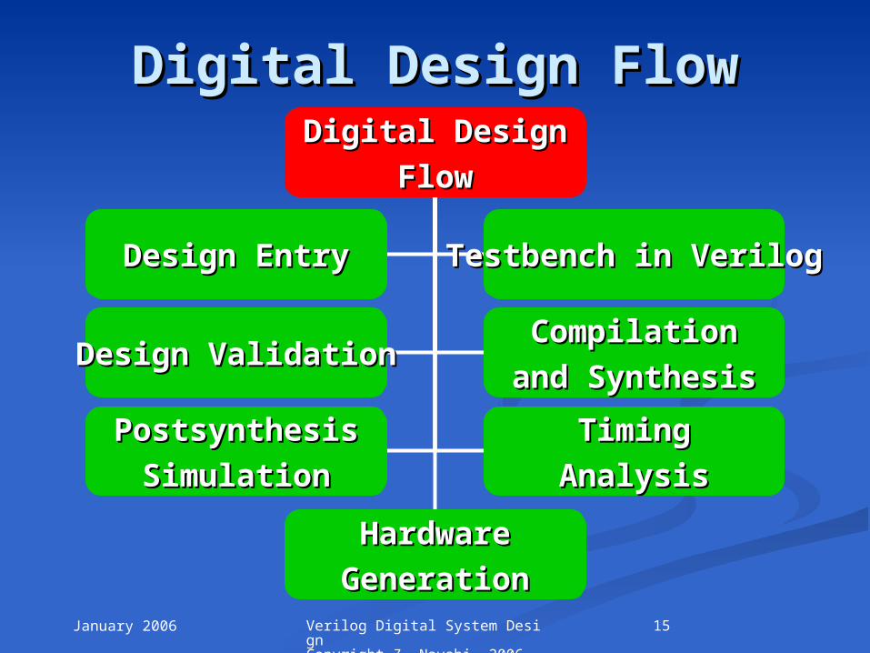
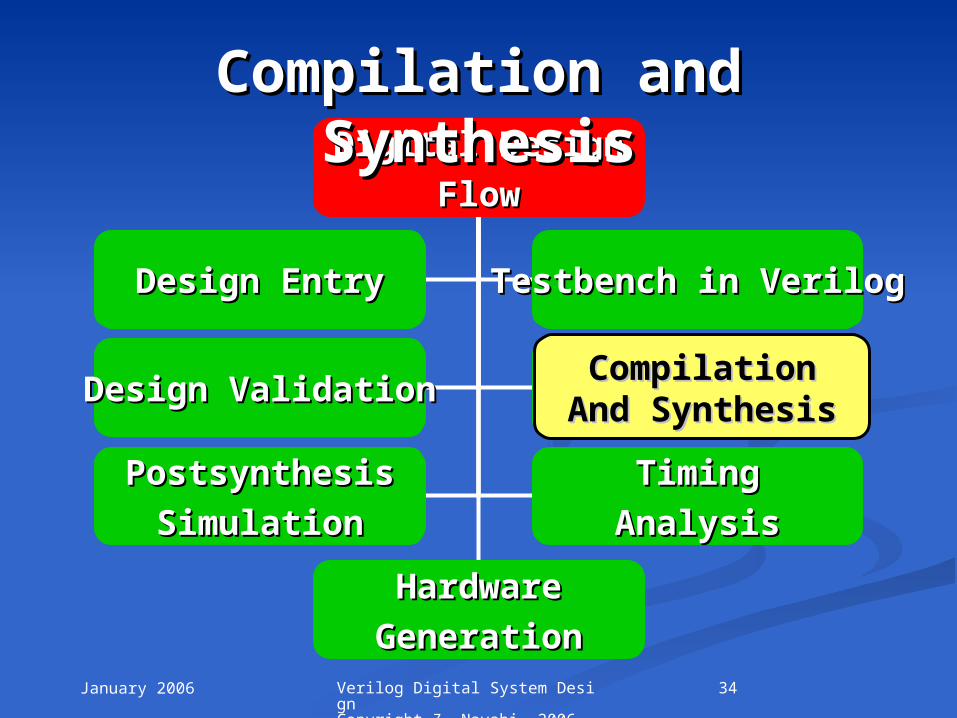
Digital DesignDigital Design
FlowFlow
HardwareHardware
GenerationGeneration
Design EntryDesign Entry Testbench in VerilogTestbench in Verilog
Design ValidationDesign ValidationCompilationCompilation
and Synthesisand Synthesis
PostsynthesisPostsynthesis
SimulationSimulationTimingTiming
AnalysisAnalysis
Digital Design FlowDigital Design Flow

January 2006 16Verilog Digital System Design Copyright Z. Navabi, 2006
Digital DesignDigital Design
FlowFlow
HardwareHardware
GenerationGeneration
Design EntryDesign Entry Testbench in VerilogTestbench in Verilog
Design ValidationDesign ValidationCompilationCompilation
and Synthesisand Synthesis
PostsynthesisPostsynthesis
SimulationSimulationTimingTiming
AnalysisAnalysis
Design EntryDesign Entry
Design EntryDesign Entry
January 2006 17Verilog Digital System Design Copyright Z. Navabi, 2006
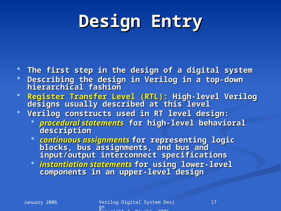
Design EntryDesign Entry
The first step in the design of a digital systemThe first step in the design of a digital system Describing the design in Verilog in a top-down Describing the design in Verilog in a top-down
hierarchical fashionhierarchical fashion Register Transfer Level (RTL):Register Transfer Level (RTL): High-level Verilog High-level Verilog
designs usually described at this leveldesigns usually described at this level Verilog constructs used in RT level design:Verilog constructs used in RT level design:
procedural statementsprocedural statements for high-level behavioral for high-level behavioral description description
continuous assignmentscontinuous assignments for representing logic for representing logic blocks, bus assignments, and bus and input/output blocks, bus assignments, and bus and input/output interconnect specificationsinterconnect specifications
instantiation statementsinstantiation statements for using lower-level for using lower-level components in an upper-level designcomponents in an upper-level design
January 2006 18Verilog Digital System Design Copyright Z. Navabi, 2006
Digital DesignDigital Design
FlowFlow
HardwareHardware
GenerationGeneration
Design EntryDesign Entry Testbench in VerilogTestbench in Verilog
Design ValidationDesign ValidationCompilationCompilation
and Synthesisand Synthesis
PostsynthesisPostsynthesis
SimulationSimulationTimingTiming
AnalysisAnalysis
Testbench in VerilogTestbench in Verilog
Testbench in VerilogTestbench in Verilog
January 2006 19Verilog Digital System Design Copyright Z. Navabi, 2006
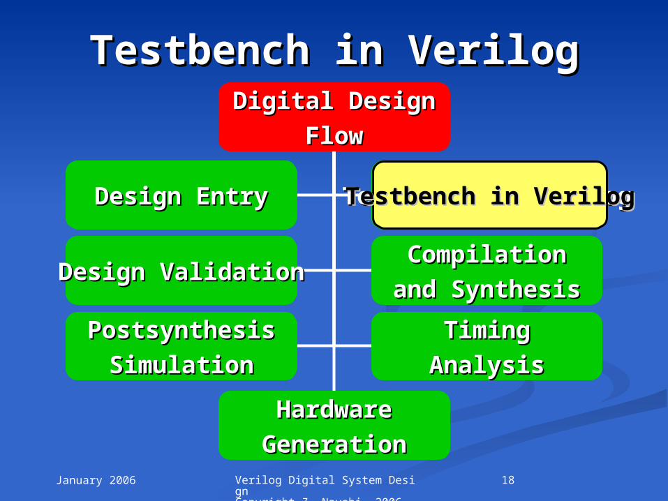
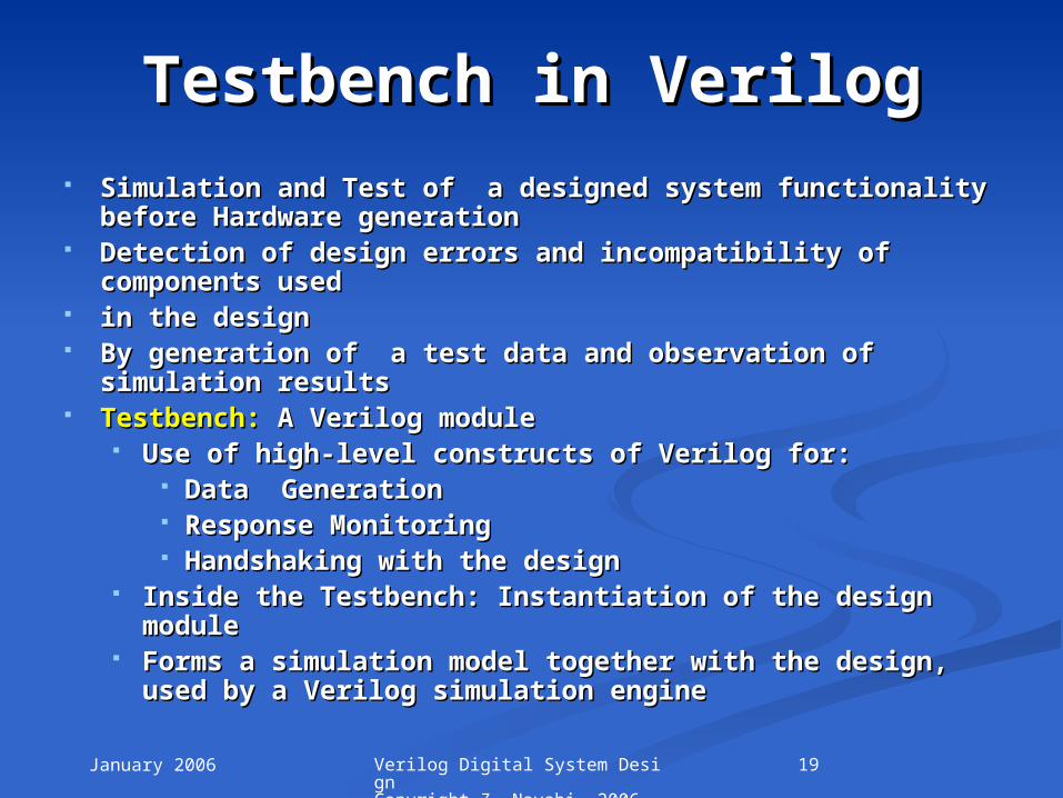
Testbench in VerilogTestbench in Verilog Simulation and Test of a designed system functionality Simulation and Test of a designed system functionality
before Hardware generationbefore Hardware generation Detection of design errors and incompatibility of Detection of design errors and incompatibility of
components used components used in the designin the design By generation of a test data and observation of By generation of a test data and observation of
simulation resultssimulation results Testbench:Testbench: A Verilog module A Verilog module
Use of high-level constructs of Verilog for:Use of high-level constructs of Verilog for: Data GenerationData Generation Response MonitoringResponse Monitoring Handshaking with the designHandshaking with the design
Inside the Testbench: Instantiation of the design Inside the Testbench: Instantiation of the design module module
Forms a simulation model together with the design, Forms a simulation model together with the design, used by a Verilog simulation engine used by a Verilog simulation engine
January 2006 20Verilog Digital System Design Copyright Z. Navabi, 2006
Digital DesignDigital Design
FlowFlow
HardwareHardware
GenerationGeneration
Design EntryDesign Entry Testbench in VerilogTestbench in Verilog
Design ValidationDesign ValidationCompilationCompilation
and Synthesisand Synthesis
PostsynthesisPostsynthesis
SimulationSimulationTimingTiming
AnalysisAnalysis
Design ValidationDesign Validation
Design ValidationDesign Validation
January 2006 21Verilog Digital System Design Copyright Z. Navabi, 2006
Design ValidationDesign Validation
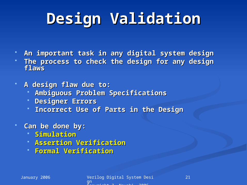
An important task in any digital system designAn important task in any digital system design The process to check the design for any design flaws The process to check the design for any design flaws
A design flaw due to:A design flaw due to: Ambiguous Problem SpecificationsAmbiguous Problem Specifications Designer ErrorsDesigner Errors Incorrect Use of Parts in the Design Incorrect Use of Parts in the Design
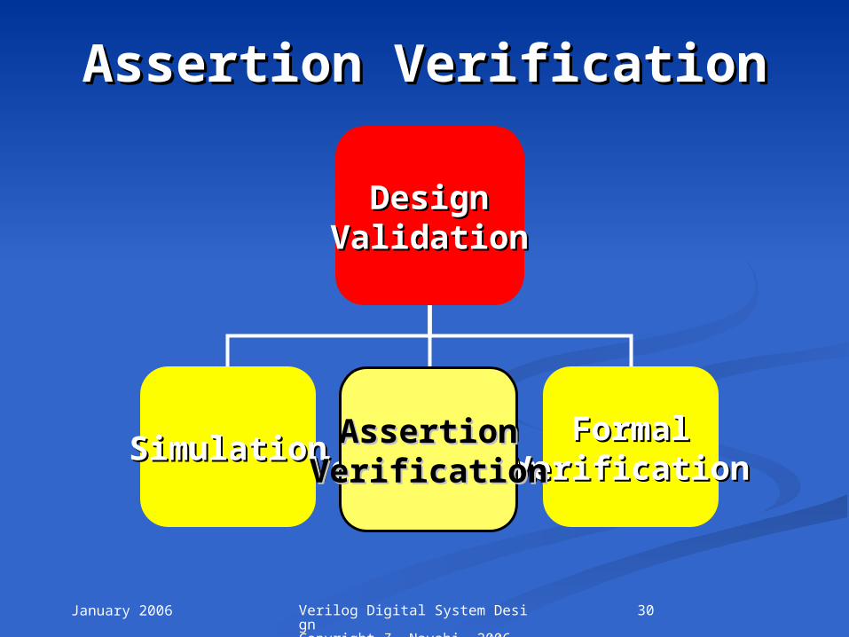
Can be done by:Can be done by: SimulationSimulation Assertion VerificationAssertion Verification Formal VerificationFormal Verification
January 2006 22Verilog Digital System Design Copyright Z. Navabi, 2006
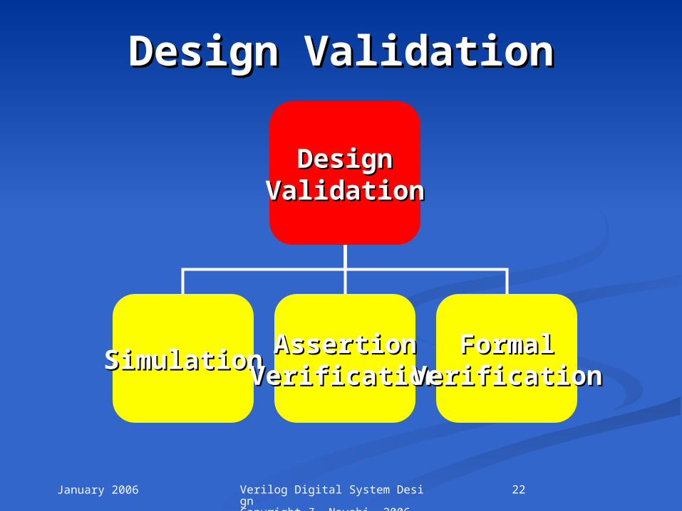
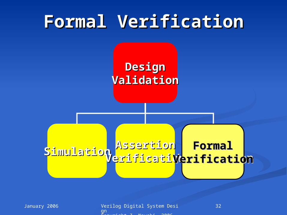
Design ValidationDesign Validation
DesignDesignValidationValidation
SimulationSimulation AssertionAssertionVerificationVerification
FormalFormalVerificationVerification
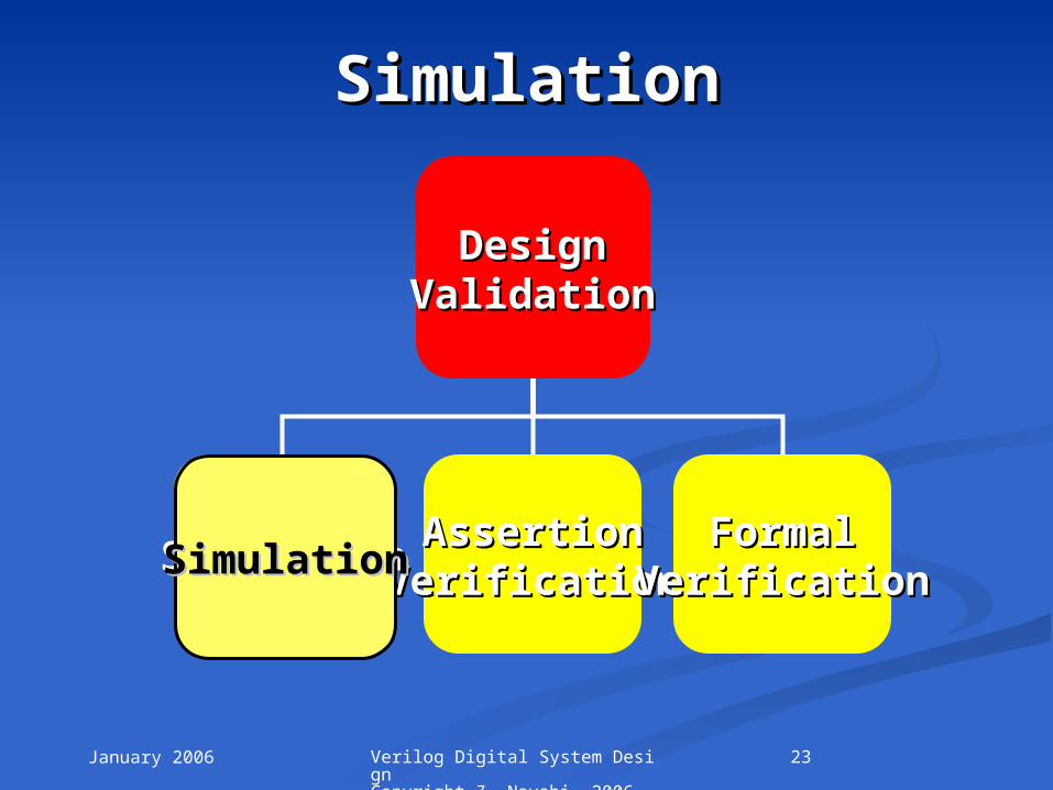
January 2006 23Verilog Digital System Design Copyright Z. Navabi, 2006
SimulationSimulation
DesignDesignValidationValidation
SimulationSimulation AssertionAssertionVerificationVerification
FormalFormalVerificationVerificationSimulationSimulation

January 2006 24Verilog Digital System Design Copyright Z. Navabi, 2006
SimulationSimulation
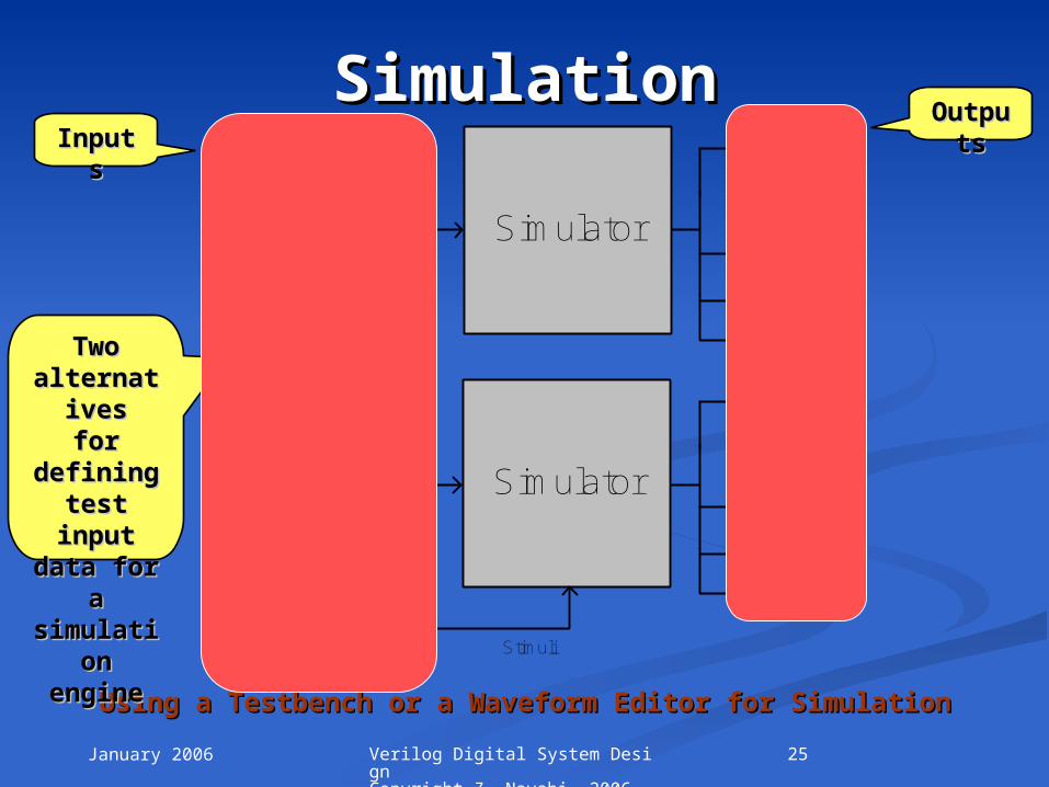
Simulation for design validation, done before a Simulation for design validation, done before a design is synthesizeddesign is synthesized
Also Referred to as RT level, or Pre-synthesis Also Referred to as RT level, or Pre-synthesis SimulationSimulation
Simulation at RTL level is accurate to the clock levelSimulation at RTL level is accurate to the clock level The advantage: its speed compared with simulations The advantage: its speed compared with simulations
at the gate or transistor levelsat the gate or transistor levels The Required Test data: generated graphically using The Required Test data: generated graphically using
waveform editors, or through a testbenchwaveform editors, or through a testbench Outputs of simulators:Outputs of simulators:
Waveforms (for visual inspection) Waveforms (for visual inspection) Text for large designs for machine processing Text for large designs for machine processing
January 2006 25Verilog Digital System Design Copyright Z. Navabi, 2006
SimulationSimulation
Using a Testbench or a Waveform Editor for Simulation Using a Testbench or a Waveform Editor for Simulation
Two Two alternatialternati
vesvesfor for
defining defining test test
input input data for data for
a a simulatiosimulation enginen engine
Testbench
Text, VCD...
Waveform
Other forms
Simulation Model
Hierachical Design
DescriptionSimulator
Waveform
Simulator
...
Simulation Model
Hierachical Design
Description
Text, VCD...
Waveform
Other forms
...
Stimuli
InputInputss
OutpuOutputsts
January 2006 26Verilog Digital System Design Copyright Z. Navabi, 2006
SimulationSimulation
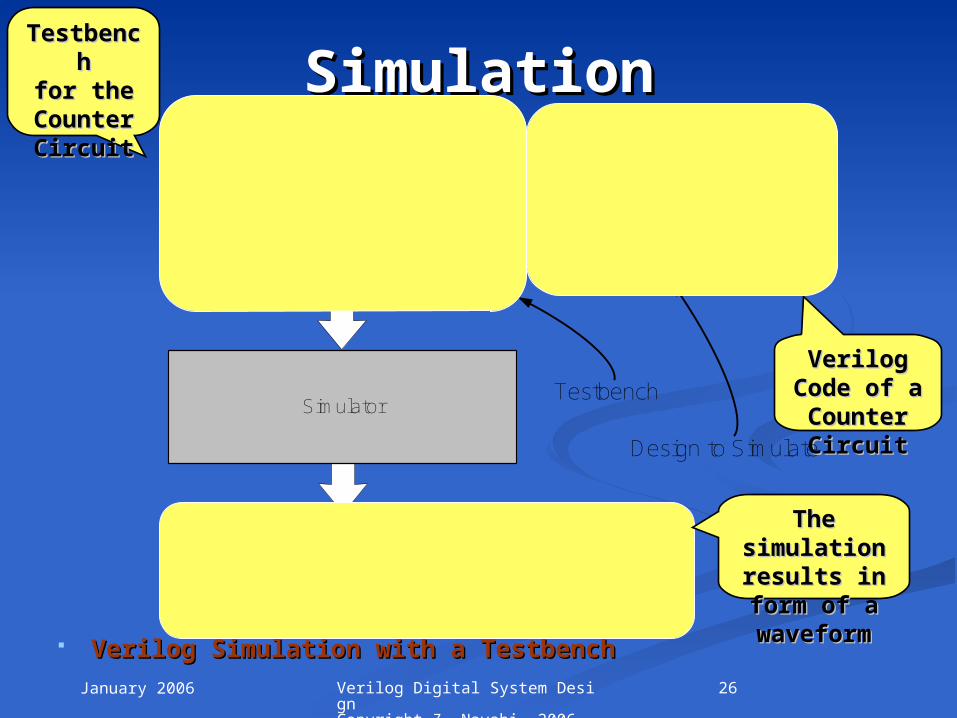
Verilog Simulation with a TestbenchVerilog Simulation with a Testbench
TestbencTestbenchh
for thefor theCounter Counter CircuitCircuit
Verilog Verilog Code of a Code of a Counter Counter CircuitCircuit
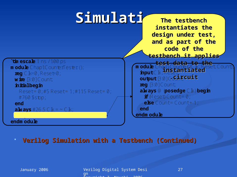
`timescale 1 ns / 100 ps module Chap1CounterTester (); reg Clk=0, Reset=0; wire [3:0] Count; initial begin Reset = 0; #5 Reset = 1; #115 Reset = 0; #760 $stop; end always #26.5 Clk = ~ Clk; Chap1Counter U1 (Clk, Reset, Count); endmodule
module Chap1Counter (Clk, Reset, Count); input Clk, Reset; output [3:0] Count; reg [3:0] Count; always @(posedge Clk) begin if (Reset) Count = 0; else Count = Count + 1; end endmodule
SimulatorTestbench
Design to Simulate
The The simulation simulation results in results in form of a form of a waveformwaveform
January 2006 27Verilog Digital System Design Copyright Z. Navabi, 2006
SimulationSimulationThe testbench The testbench instantiates the instantiates the
design under test, design under test, and as part of the and as part of the
code of the testbench code of the testbench it applies test data to it applies test data to
the instantiated the instantiated circuitcircuit..
Verilog Simulation with a Testbench (Continued)Verilog Simulation with a Testbench (Continued)
`timescale 1 ns / 100 ps module Chap1CounterTester (); reg Clk=0, Reset=0; wire [3:0] Count; initial begin Reset = 0; #5 Reset = 1; #115 Reset = 0; #760 $stop; end always #26.5 Clk = ~ Clk; Chap1Counter U1 (Clk, Reset, Count); endmodule
module Chap1Counter (Clk, Reset, Count); input Clk, Reset; output [3:0] Count; reg [3:0] Count; always @(posedge Clk) begin if (Reset) Count = 0; else Count = Count + 1; end endmodule
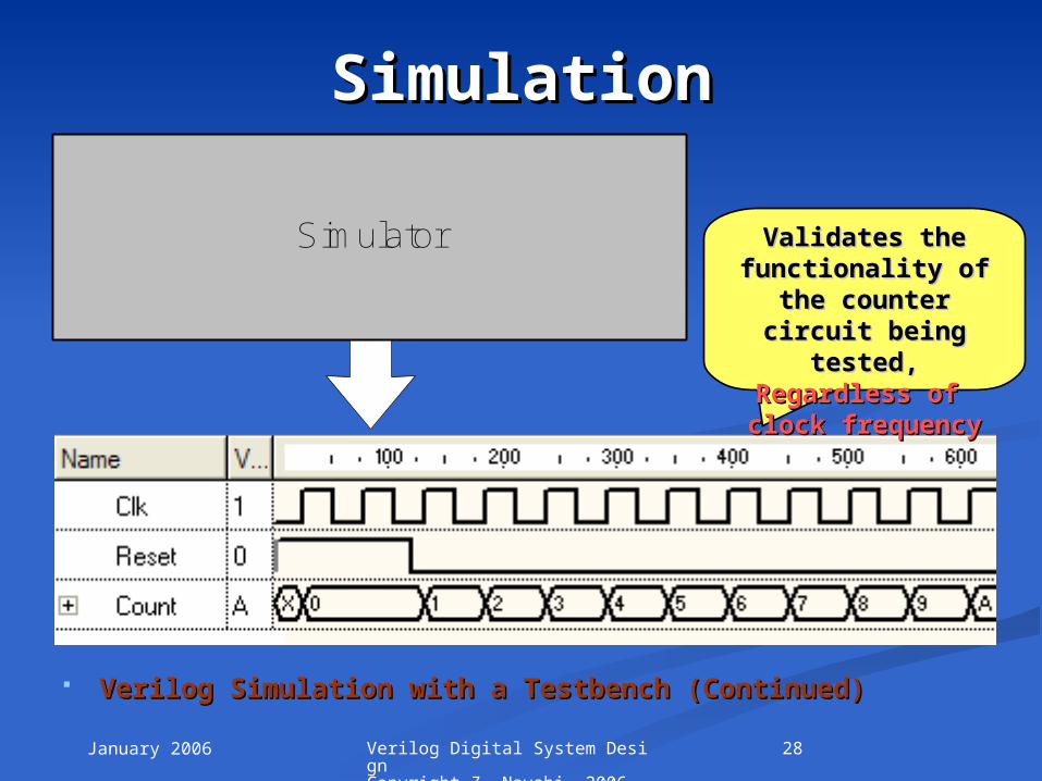
January 2006 28Verilog Digital System Design Copyright Z. Navabi, 2006
Simulator
SimulationSimulation
Validates the Validates the functionality of functionality of
the counter circuit the counter circuit being tested, being tested, Regardless of Regardless of
clock frequencyclock frequency
Verilog Simulation with a Testbench (Continued)Verilog Simulation with a Testbench (Continued)
January 2006 29Verilog Digital System Design Copyright Z. Navabi, 2006
SimulationSimulation
Obviously, an actual hardware component behaves Obviously, an actual hardware component behaves differently. differently.
Based on the timing and delays of the parts used, Based on the timing and delays of the parts used, there will be a nonzero delay between the active edge there will be a nonzero delay between the active edge of the clock and the counter output. of the clock and the counter output.
Furthermore, if the clock frequency applied to an Furthermore, if the clock frequency applied to an actual part is too fast for propagation of values actual part is too fast for propagation of values within the gates and transistors of a design, the within the gates and transistors of a design, the output of the design becomes unpredictable. output of the design becomes unpredictable.
The simulation shown here is not provided with the The simulation shown here is not provided with the details of the timing of the hardware being details of the timing of the hardware being simulated. simulated.
Therefore, potential timing problems of the hardware Therefore, potential timing problems of the hardware that are due to gate delays cannot be detected. that are due to gate delays cannot be detected.
This is typical of a presynthesis or high-level This is typical of a presynthesis or high-level behavioral simulation.behavioral simulation.
January 2006 30Verilog Digital System Design Copyright Z. Navabi, 2006
Assertion VerificationAssertion Verification
DesignDesignValidationValidation
SimulationSimulation AssertionAssertionVerificationVerification
FormalFormalVerificationVerification
AssertionAssertionVerificationVerification
January 2006 31Verilog Digital System Design Copyright Z. Navabi, 2006
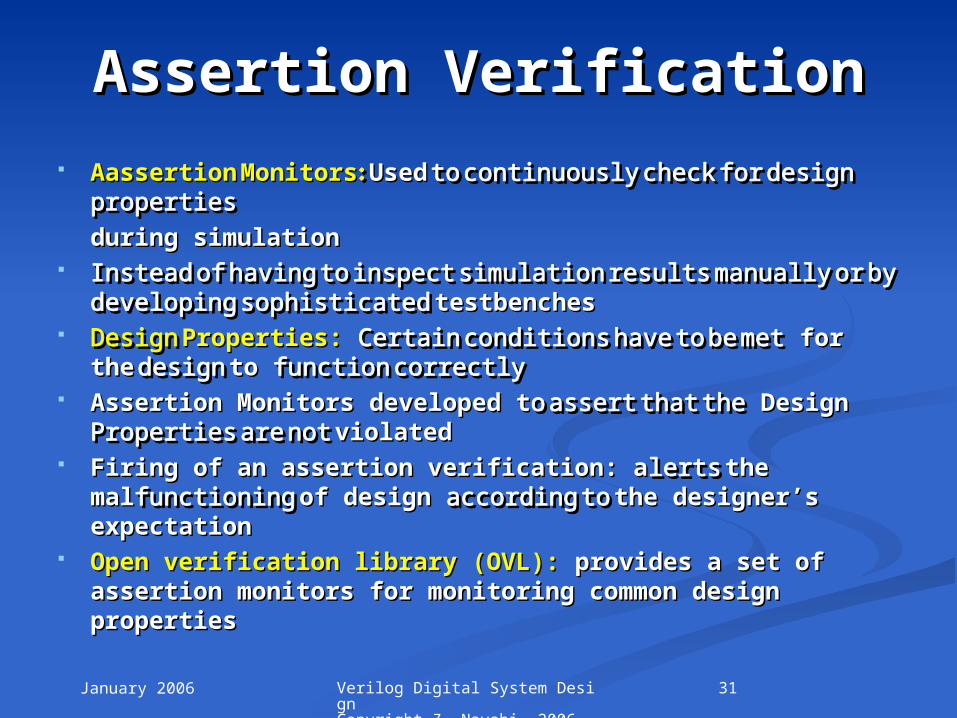
Assertion VerificationAssertion Verification AAassertionassertion MonitorsMonitors:: UsedUsed to continuously check for to continuously check for
design properties design properties
during simulationduring simulation Instead of having to inspect simulation results Instead of having to inspect simulation results
manually or by developing sophisticated manually or by developing sophisticated testbenchestestbenches DDesign esign Properties: Properties: CCertain conditions have to be metertain conditions have to be met
for thefor the design design to to function correctlyfunction correctly Assertion Monitors developed tAssertion Monitors developed to assert that theo assert that the Design Design
PProperties are not roperties are not violatedviolated Firing of an assertion verification: aFiring of an assertion verification: alerts lerts the the
malmalfunctioning functioning of design of design according to according to the designer’s the designer’s expectationexpectation
Open verification library (OVL):Open verification library (OVL): provides a set of provides a set of assertion monitors for monitoring common design assertion monitors for monitoring common design propertiesproperties
January 2006 32Verilog Digital System Design Copyright Z. Navabi, 2006
Formal VerificationFormal Verification
DesignDesignValidationValidation
SimulationSimulation AssertionAssertionVerificationVerification
FormalFormalVerificationVerification
FormalFormalVerificationVerification
January 2006 33Verilog Digital System Design Copyright Z. Navabi, 2006
Formal VerificationFormal Verification
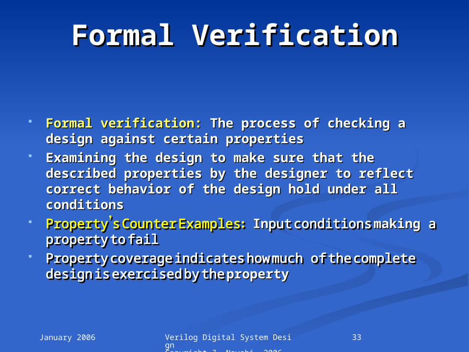
Formal verification:Formal verification: The process of checking a design The process of checking a design against certain propertiesagainst certain properties
Examining the design to make sure that the Examining the design to make sure that the described properties by the designer to reflect described properties by the designer to reflect correct behavior of the design hold under all correct behavior of the design hold under all conditionsconditions
PProperty’s roperty’s CCounter ounter EExamples:xamples: InInput conditions put conditions making making a property to faila property to fail
Property coverage indicates how muchProperty coverage indicates how much of the of the complete design is exercised by the complete design is exercised by the propertyproperty
January 2006 34Verilog Digital System Design Copyright Z. Navabi, 2006
Digital DesignDigital Design
FlowFlow
HardwareHardware
GenerationGeneration
Design EntryDesign Entry Testbench in VerilogTestbench in Verilog
Design ValidationDesign ValidationCompilationCompilation
and Synthesisand Synthesis
PostsynthesisPostsynthesis
SimulationSimulationTimingTiming
AnalysisAnalysis
Compilation and Compilation and SynthesisSynthesis
CompilationCompilationAnd SynthesisAnd Synthesis
January 2006 35Verilog Digital System Design Copyright Z. Navabi, 2006
Compilation and Compilation and SynthesisSynthesis
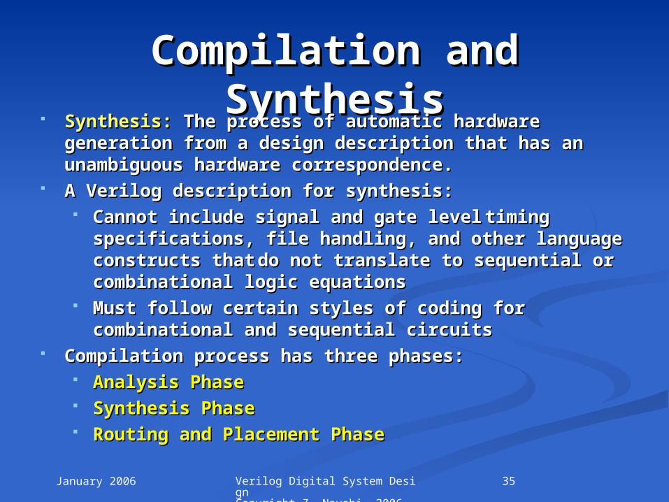
Synthesis:Synthesis: The process of automatic hardware The process of automatic hardware generation from a design description that has an generation from a design description that has an unambiguous hardware correspondence.unambiguous hardware correspondence.
A Verilog description for synthesis:A Verilog description for synthesis: Cannot include signal and gate levelCannot include signal and gate level timing timing
specifications, file handling, and other language specifications, file handling, and other language constructs thatconstructs that do not translate to sequential or do not translate to sequential or combinational logic equationscombinational logic equations
Must follow certain styles of coding for Must follow certain styles of coding for combinational and sequential circuitscombinational and sequential circuits
Compilation process has three phases:Compilation process has three phases: Analysis PhaseAnalysis Phase Synthesis PhaseSynthesis Phase Routing and Placement PhaseRouting and Placement Phase

January 2006 36Verilog Digital System Design Copyright Z. Navabi, 2006
Compilation and Compilation and SynthesisSynthesis
Compilation and Synthesis ProcessCompilation and Synthesis Process
Design Specification
Comp1 U1 (. . .);Comp2 U2 (. . .);. . .Compn Un (. . .);
Analysis
Generic Hardware
Generation
Logic Optimization
Binding
Routing and
Placement
Timing Analysis
Target Hardware Specification
Pd Su
Intermediate Format
Synthesis
T = … ; T = ...
Operating Condition
Chip Manufacturing
orDevice
Programming
always (posedge clk) begin . . . end
if (…) bus = w;else . . .
module design (. . .); assign . . . always . . . compi (. . .)endmodule
Input: Input: Hardware Hardware
description description consisting of consisting of
various various levels oflevels of VerilogVerilog
Output: Output: A detailed A detailed hardware hardware
for for programmiprogramming an FPLD ng an FPLD
or or manufacturmanufacturing aning an ASICASIC
The The compilation compilation
process and a process and a graphical graphical
representatiorepresentation for each of n for each of
the the compilation compilation
phase outputsphase outputs
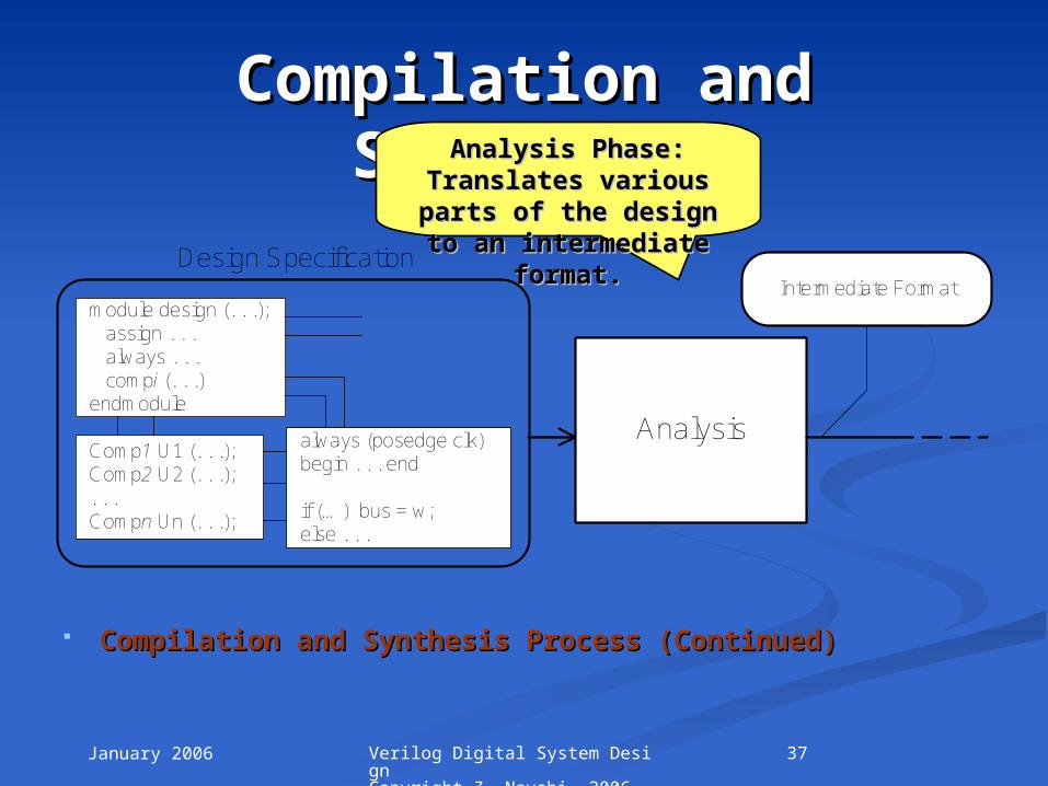
January 2006 37Verilog Digital System Design Copyright Z. Navabi, 2006
Compilation and Compilation and SynthesisSynthesis
Compilation and Synthesis Process (Continued)Compilation and Synthesis Process (Continued)
Design Specification
Comp1 U1 (. . .);Comp2 U2 (. . .);. . .Compn Un (. . .);
Analysis
Intermediate Format
always (posedge clk) begin . . . end
if (…) bus = w;else . . .
module design (. . .); assign . . . always . . . compi (. . .)endmodule
Analysis Phase: Analysis Phase: Translates various Translates various
parts of the design to parts of the design to an intermediatean intermediate
format.format.
January 2006 38Verilog Digital System Design Copyright Z. Navabi, 2006
Generic Hardware
Generation
Logic Optimization
Binding
Target Hardware Specification
Synthesis
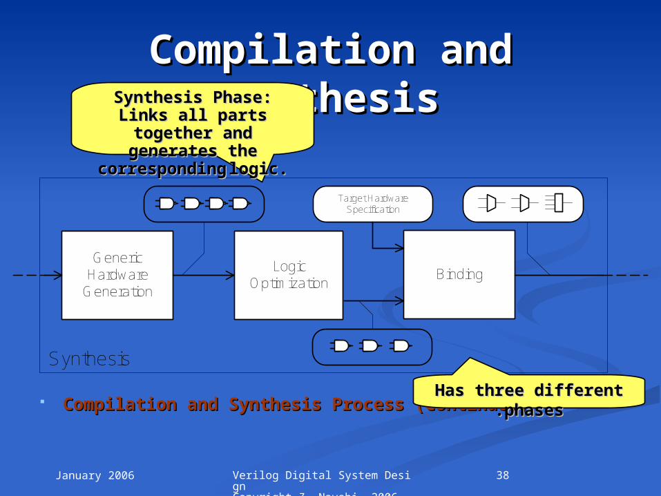
Compilation and Compilation and SynthesisSynthesis
Compilation and Synthesis Process (Continued)Compilation and Synthesis Process (Continued)
Synthesis Phase: Links Synthesis Phase: Links all parts together and all parts together and
generates the generates the correspondingcorresponding logic.logic.
Has three different Has three different phasesphases..
January 2006 39Verilog Digital System Design Copyright Z. Navabi, 2006
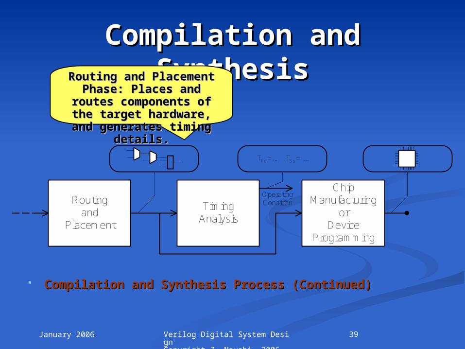
Compilation and Compilation and SynthesisSynthesis
Compilation and Synthesis Process (Continued)Compilation and Synthesis Process (Continued)
Routing and Placement Routing and Placement Phase: Places and Phase: Places and
routes components of routes components of the target hardware,the target hardware, and generates timing and generates timing
details.details.
Routing and
Placement
Timing Analysis
Pd SuT = … ; T = ...
Operating Condition
Chip Manufacturing
orDevice
Programming

January 2006 40Verilog Digital System Design Copyright Z. Navabi, 2006
Compilation and Compilation and SynthesisSynthesisCompilation Compilation and Synthesisand Synthesis
Routing andRouting and
PlacementPlacement
AnalysisAnalysisGeneric HardwareGeneric Hardware
GenerationGeneration
LogicLogic
OptimizationOptimizationBindingBinding

January 2006 41Verilog Digital System Design Copyright Z. Navabi, 2006
AnalysisAnalysisCompilation Compilation and Synthesisand Synthesis
Routing andRouting and
PlacementPlacement
AnalysisAnalysisGeneric HardwareGeneric Hardware
GenerationGeneration
LogicLogic
OptimizationOptimizationBindingBinding
AnalysisAnalysis
January 2006 42Verilog Digital System Design Copyright Z. Navabi, 2006
AnalysisAnalysis
Before the complete design is turned into hardwareBefore the complete design is turned into hardware Analyzing the design and generating a uniform Analyzing the design and generating a uniform
format for allformat for all parts ofparts of itit Also checks the syntax and semantics of the input Also checks the syntax and semantics of the input
Verilog codeVerilog code
January 2006 43Verilog Digital System Design Copyright Z. Navabi, 2006
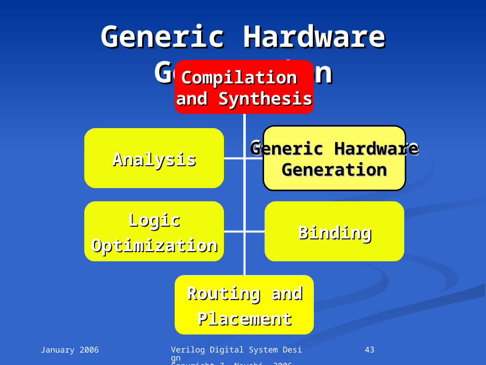
Generic Hardware Generic Hardware GenerationGenerationCompilation Compilation
and Synthesisand Synthesis
Routing andRouting and
PlacementPlacement
AnalysisAnalysisGeneric HardwareGeneric Hardware
GenerationGeneration
LogicLogic
OptimizationOptimizationBindingBinding
Generic HardwareGeneric HardwareGenerationGeneration

January 2006 44Verilog Digital System Design Copyright Z. Navabi, 2006
Generic Hardware Generic Hardware GenerationGeneration
Generic Hardware Generation: Generic Hardware Generation: Turning the design Turning the design into a generic hardware format such as a set of into a generic hardware format such as a set of Boolean expressions or a netlist of basic gatesBoolean expressions or a netlist of basic gates
January 2006 45Verilog Digital System Design Copyright Z. Navabi, 2006
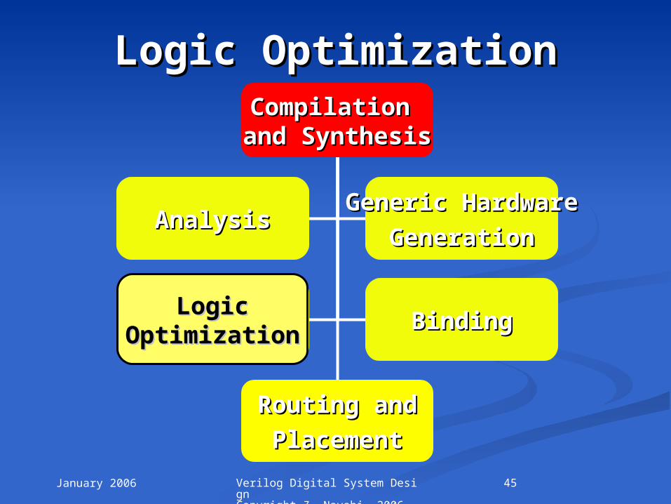
Logic OptimizationLogic OptimizationCompilation Compilation and Synthesisand Synthesis
Routing andRouting and
PlacementPlacement
AnalysisAnalysisGeneric HardwareGeneric Hardware
GenerationGeneration
LogicLogic
OptimizationOptimizationBindingBindingLogicLogic
OptimizationOptimization
January 2006 46Verilog Digital System Design Copyright Z. Navabi, 2006
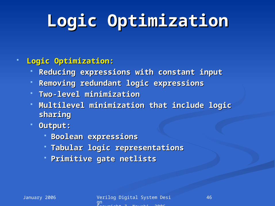
Logic OptimizationLogic Optimization
Logic Optimization:Logic Optimization: Reducing expressions with constant inputReducing expressions with constant input Removing redundant logic expressionsRemoving redundant logic expressions Two-level minimizationTwo-level minimization Multilevel minimization that include logic sharingMultilevel minimization that include logic sharing Output: Output:
Boolean expressions Boolean expressions Tabular logic representationsTabular logic representations Primitive gate netlistsPrimitive gate netlists
January 2006 47Verilog Digital System Design Copyright Z. Navabi, 2006
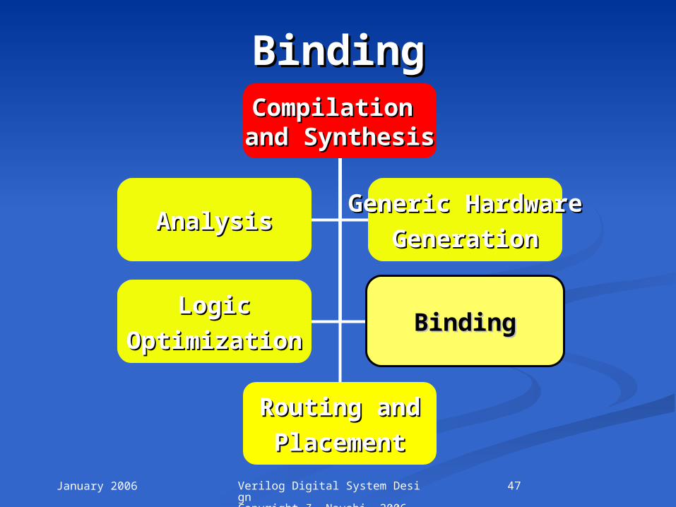
BindingBindingCompilation Compilation and Synthesisand Synthesis
Routing andRouting and
PlacementPlacement
AnalysisAnalysisGeneric HardwareGeneric Hardware
GenerationGeneration
LogicLogic
OptimizationOptimizationBindingBindingBindingBinding

January 2006 48Verilog Digital System Design Copyright Z. Navabi, 2006
BindingBinding
Binding:Binding: Decide exactly what logic elementsDecide exactly what logic elements and cells are and cells are
needed for the realization of the circuit using needed for the realization of the circuit using information from target hardwareinformation from target hardware
OOutput is specific to theutput is specific to the FPLD, ASIC, or custom IC FPLD, ASIC, or custom IC being usedbeing used
January 2006 49Verilog Digital System Design Copyright Z. Navabi, 2006
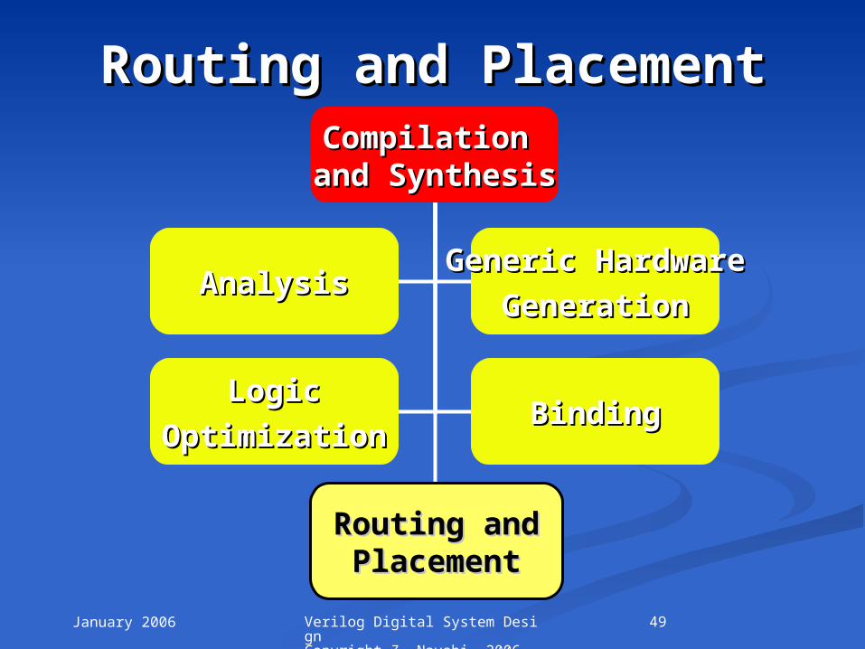
Routing and PlacementRouting and PlacementCompilation Compilation and Synthesisand Synthesis
Routing andRouting and
PlacementPlacement
AnalysisAnalysisGeneric HardwareGeneric Hardware
GenerationGeneration
LogicLogic
OptimizationOptimizationBindingBinding
Routing andRouting andPlacementPlacement

January 2006 50Verilog Digital System Design Copyright Z. Navabi, 2006
Routing and PlacementRouting and Placement
DDecides on the placement of cells of the target ecides on the placement of cells of the target hardwarehardware
Determines Determines wiring of wiring of inputs and outputs of the cells inputs and outputs of the cells through wiring channels and switching areas of the through wiring channels and switching areas of the target target hardwarehardware
The output is specific to the hardware being used and The output is specific to the hardware being used and can be used for programming an FPLD or can be used for programming an FPLD or manufacturing an ASIC.manufacturing an ASIC.

January 2006 51Verilog Digital System Design Copyright Z. Navabi, 2006
Routing and PlacementRouting and Placement
An Example Synthesis RunAn Example Synthesis Run
module Chap1Counter (Clk, Reset, Count); input Clk, Reset; output [3:0] Count; reg [3:0] Count; always @(posedge Clk) begin if (Reset) Count = 0; else Count = Count + 1; end endmodule
Synthesis Tool
Target hardware specification
List of primitive components - Flip-flops - Logic elements Timing specifications - Pin-to-pin timing
Design to Synthesize
An example An example of a of a
synthesis synthesis run: The run: The counter counter circuit is circuit is
being being synthesizedsynthesized
January 2006 52Verilog Digital System Design Copyright Z. Navabi, 2006
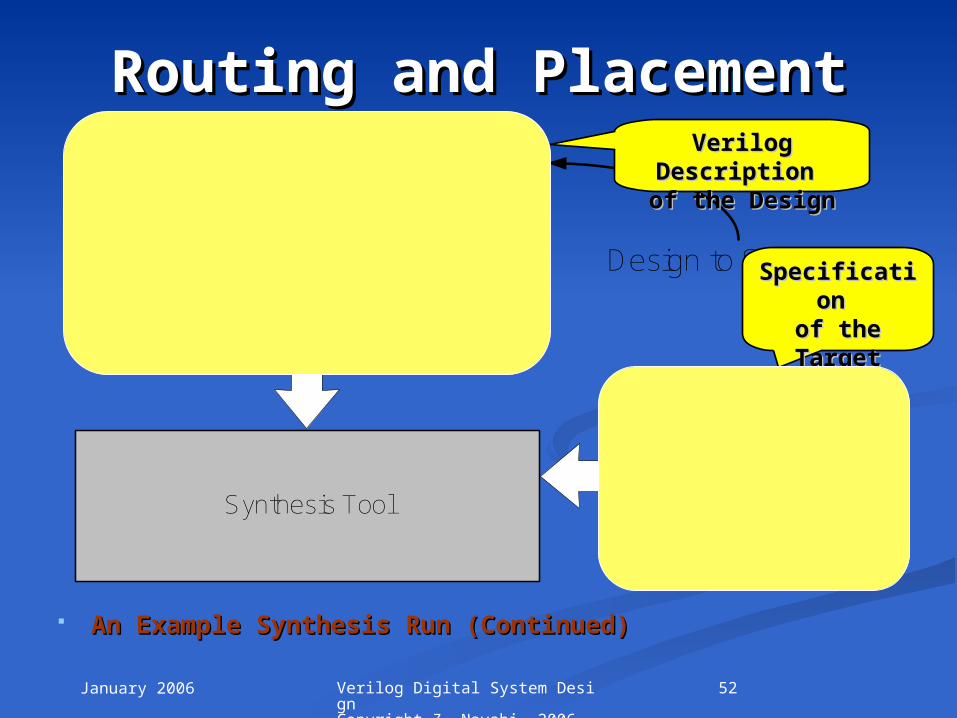
Routing and PlacementRouting and Placement
An Example Synthesis Run (Continued)An Example Synthesis Run (Continued)
module Chap1Counter (Clk, Reset, Count); input Clk, Reset; output [3:0] Count; reg [3:0] Count; always @(posedge Clk) begin if (Reset) Count = 0; else Count = Count + 1; end endmodule
Synthesis Tool
Target hardware specification
List of primitive components - Flip-flops - Logic elements Timing specifications - Pin-to-pin timing
Design to Synthesize
Verilog Verilog Description Description of the Designof the Design
SpecificatioSpecification n
of the of the Target Target
Hardware Hardware

January 2006 53Verilog Digital System Design Copyright Z. Navabi, 2006
Synthesis Tool
Routing and PlacementRouting and Placement
An Example Synthesis Run (Continued)An Example Synthesis Run (Continued)
The output The output of synthesis of synthesis
tooltool
A list of gates A list of gates and flip-flops and flip-flops
available in the available in the target hardware target hardware
and their and their interconnections interconnections
January 2006 54Verilog Digital System Design Copyright Z. Navabi, 2006
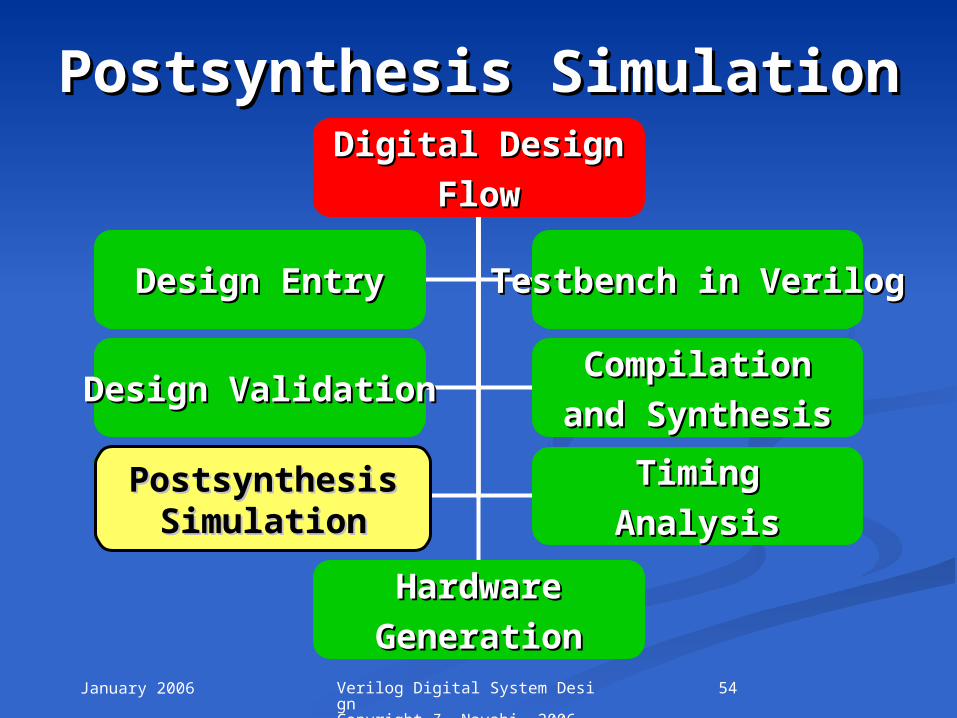
Digital DesignDigital Design
FlowFlow
HardwareHardware
GenerationGeneration
Design EntryDesign Entry Testbench in VerilogTestbench in Verilog
Design ValidationDesign ValidationCompilationCompilation
and Synthesisand Synthesis
PostsynthesisPostsynthesis
SimulationSimulationTimingTiming
AnalysisAnalysisPostsynthesisPostsynthesis
SimulationSimulation
Postsynthesis SimulationPostsynthesis Simulation
January 2006 55Verilog Digital System Design Copyright Z. Navabi, 2006
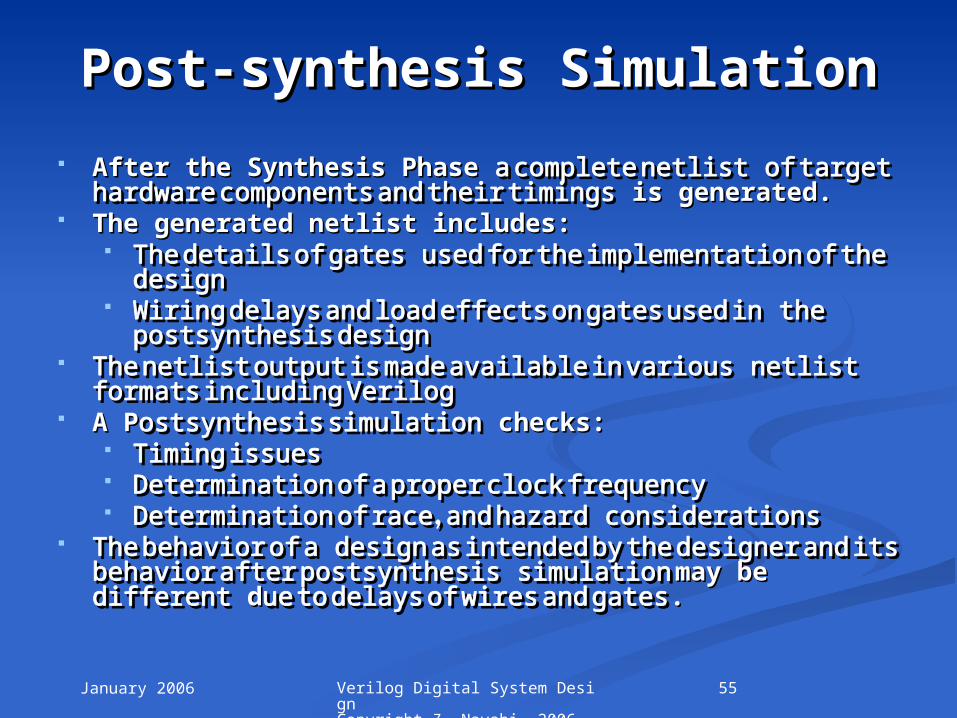
Post-synthesis SimulationPost-synthesis Simulation
After the Synthesis Phase After the Synthesis Phase a complete netlista complete netlist of target of target hardware components and their timingshardware components and their timings is is generated.generated.
The generated netlist includes:The generated netlist includes: The details of gatesThe details of gates used for the implementation used for the implementation
of the designof the design WWiring delays and load effects on gates used iniring delays and load effects on gates used in
the postsynthesis designthe postsynthesis design The netlist output is made available in variousThe netlist output is made available in various netlist netlist
formats including Verilogformats including Verilog A PA Postsynthesis simulationostsynthesis simulation checks: checks:
Timing issuesTiming issues DDetermination of a proper clock frequency etermination of a proper clock frequency DDetermination of race, and hazardetermination of race, and hazard considerations considerations
TThe behavior of ahe behavior of a design as intended by the designer design as intended by the designer and its behavior after postsynthesisand its behavior after postsynthesis simulation simulation may may bebe different different d due to delays of wires and gatesue to delays of wires and gates..
January 2006 56Verilog Digital System Design Copyright Z. Navabi, 2006
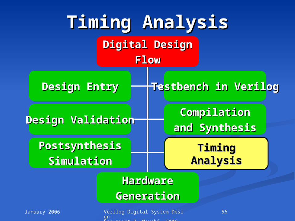
Digital DesignDigital Design
FlowFlow
HardwareHardware
GenerationGeneration
Design EntryDesign Entry Testbench in VerilogTestbench in Verilog
Design ValidationDesign ValidationCompilationCompilation
and Synthesisand Synthesis
PostsynthesisPostsynthesis
SimulationSimulationTimingTiming
AnalysisAnalysis
Timing AnalysisTiming Analysis
TimingTimingAnalysisAnalysis
January 2006 57Verilog Digital System Design Copyright Z. Navabi, 2006
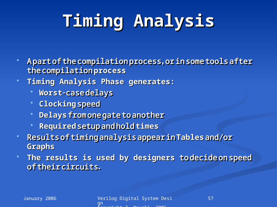
Timing AnalysisTiming Analysis
AA part of the compilation process, or in some tools part of the compilation process, or in some tools after the compilation after the compilation processprocess
Timing Analysis Phase generates:Timing Analysis Phase generates: WorstWorst-case delays -case delays ClockingClocking speed speed DelaysDelays from one gate to another from one gate to another RequiredRequired setup and hold setup and hold timestimes
Results of timing analysis appear in Results of timing analysis appear in TablesTables and/or and/or GraphsGraphs
The results is used by designers The results is used by designers to decide on speed to decide on speed of their circuits.of their circuits.
January 2006 58Verilog Digital System Design Copyright Z. Navabi, 2006
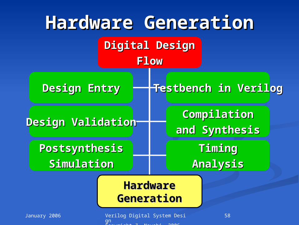
Digital DesignDigital Design
FlowFlow
HardwareHardware
GenerationGeneration
Design EntryDesign Entry Testbench in VerilogTestbench in Verilog
Design ValidationDesign ValidationCompilationCompilation
and Synthesisand Synthesis
PostsynthesisPostsynthesis
SimulationSimulationTimingTiming
AnalysisAnalysis
Hardware GenerationHardware Generation
HardwareHardwareGenerationGeneration

January 2006 59Verilog Digital System Design Copyright Z. Navabi, 2006
Hardware GenerationHardware Generation
LastLast stage in an automated Verilog-based design stage in an automated Verilog-based design Generates a netlist for ASIC manufacturing, a Generates a netlist for ASIC manufacturing, a
program for programming FPLDs, or layout of custom program for programming FPLDs, or layout of custom IC cellsIC cells
January 2006 60Verilog Digital System Design Copyright Z. Navabi, 2006
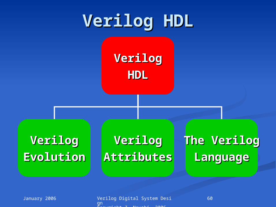
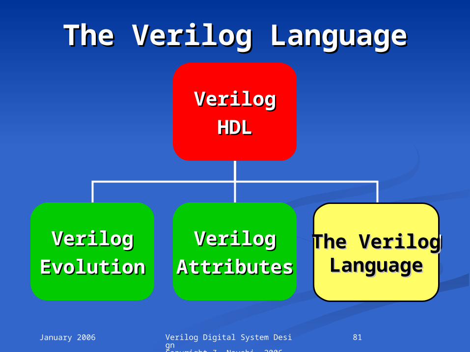
Verilog HDLVerilog HDL
VerilogVerilog
HDLHDL
VerilogVerilog
EvolutionEvolutionVerilogVerilog
AttributesAttributesThe VerilogThe Verilog
LanguageLanguage
January 2006 61Verilog Digital System Design Copyright Z. Navabi, 2006
Verilog HDLVerilog HDL
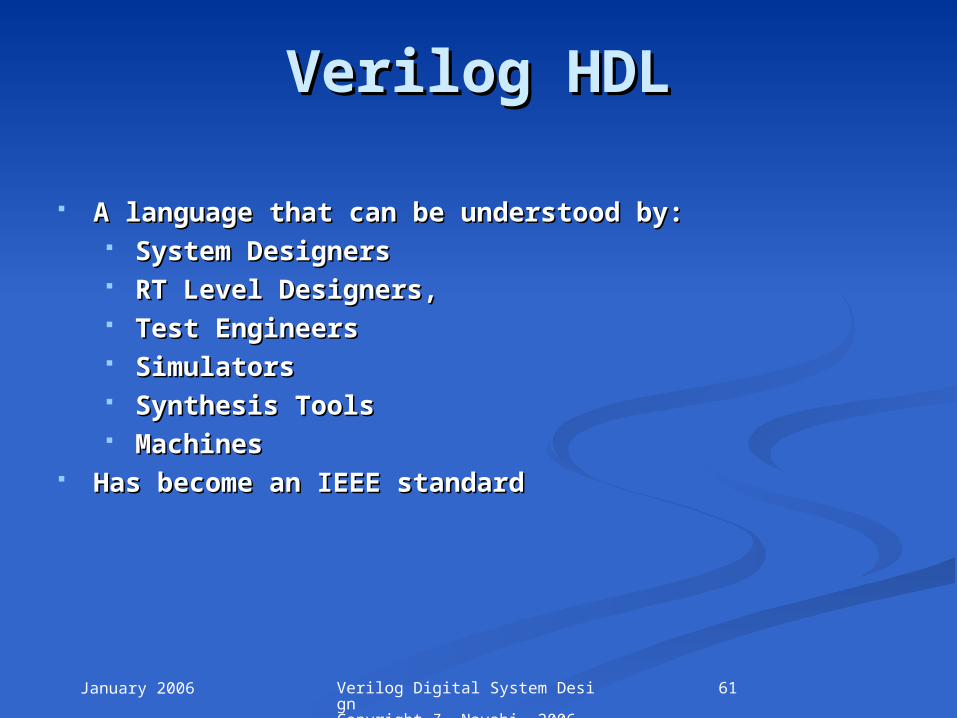
A language that can be understood by:A language that can be understood by: System Designers System Designers RT Level Designers, RT Level Designers, Test Engineers Test Engineers Simulators Simulators Synthesis ToolsSynthesis Tools Machines Machines
Has become an IEEE standardHas become an IEEE standard

January 2006 62Verilog Digital System Design Copyright Z. Navabi, 2006
Verilog EvolutionVerilog Evolution
VerilogVerilog
HDLHDL
VerilogVerilog
EvolutionEvolutionVerilogVerilog
AttributesAttributesThe VerilogThe Verilog
LanguageLanguageVerilogVerilog
EvolutionEvolution

January 2006 63Verilog Digital System Design Copyright Z. Navabi, 2006
Verilog EvolutionVerilog Evolution Designed in early Designed in early 19841984 by by Gateway Design AutomationGateway Design Automation Originally used as a simulation and verification toolOriginally used as a simulation and verification tool After the initial acceptance of this language by electronic After the initial acceptance of this language by electronic
industry, a fault simulator, a timing analyzer, and later in industry, a fault simulator, a timing analyzer, and later in 1987, a synthesis tool was developed based on this 1987, a synthesis tool was developed based on this language.language.
Since acquiring Gateway Design Automation and its Verilog-Since acquiring Gateway Design Automation and its Verilog-based tools by Cadence Design System, based tools by Cadence Design System, CadenceCadence has been a has been a strong force behind popularizing the Verilog hardware strong force behind popularizing the Verilog hardware description language.description language.
In 1987 VHDL became an IEEE standard hardware In 1987 VHDL became an IEEE standard hardware description language.description language.
VHDL was adapted by the U.S. government for related VHDL was adapted by the U.S. government for related projects and contracts.projects and contracts.
In an effort for popularizing Verilog, in 1990, In an effort for popularizing Verilog, in 1990, OVI (Open OVI (Open Verilog International)Verilog International) was formed and Verilog was placed in was formed and Verilog was placed in public domain.public domain.
In 1993, efforts for standardization of this language started. In 1993, efforts for standardization of this language started. Verilog became the IEEE standard, Verilog became the IEEE standard, IEEE Std. 1364-1995IEEE Std. 1364-1995, in , in 1995.1995.

January 2006 64Verilog Digital System Design Copyright Z. Navabi, 2006
Verilog EvolutionVerilog Evolution
Verilog-2001: Verilog-2001: A new version of Verilog approved by A new version of Verilog approved by IEEE in 2001IEEE in 2001
Additional Features of Verilog-2001:Additional Features of Verilog-2001: New features for external file access for read and New features for external file access for read and
writewrite Library managementLibrary management Constructs for design ConfigurationConstructs for design Configuration Higher abstraction level constructsHigher abstraction level constructs Constructs for specification of iterative structuresConstructs for specification of iterative structures
January 2006 65Verilog Digital System Design Copyright Z. Navabi, 2006
Verilog AttributesVerilog Attributes
VerilogVerilog
HDLHDL
VerilogVerilog
EvolutionEvolutionVerilogVerilog
AttributesAttributesThe VerilogThe Verilog
LanguageLanguageVerilogVerilog
AttributesAttributes
January 2006 66Verilog Digital System Design Copyright Z. Navabi, 2006
Verilog AttributesVerilog Attributes
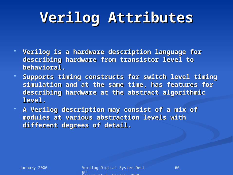
Verilog is a hardware description language for Verilog is a hardware description language for describing hardware from transistor level to describing hardware from transistor level to behavioral.behavioral.
Supports timing constructs for switch level timing Supports timing constructs for switch level timing simulation and at the same time, has features for simulation and at the same time, has features for describing hardware at the abstract algorithmic describing hardware at the abstract algorithmic level.level.
A Verilog description may consist of a mix of modules A Verilog description may consist of a mix of modules at various abstraction levels with different degrees of at various abstraction levels with different degrees of detail.detail.
January 2006 67Verilog Digital System Design Copyright Z. Navabi, 2006
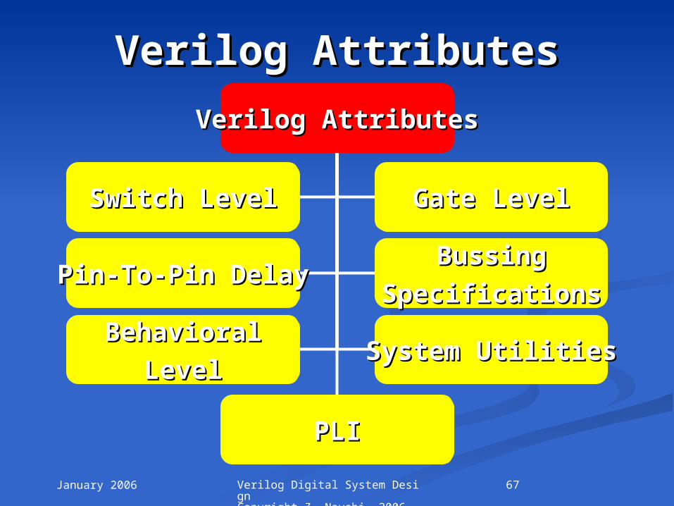
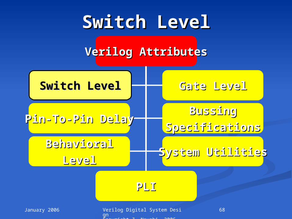
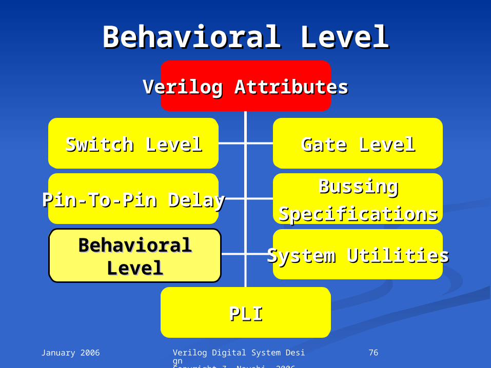
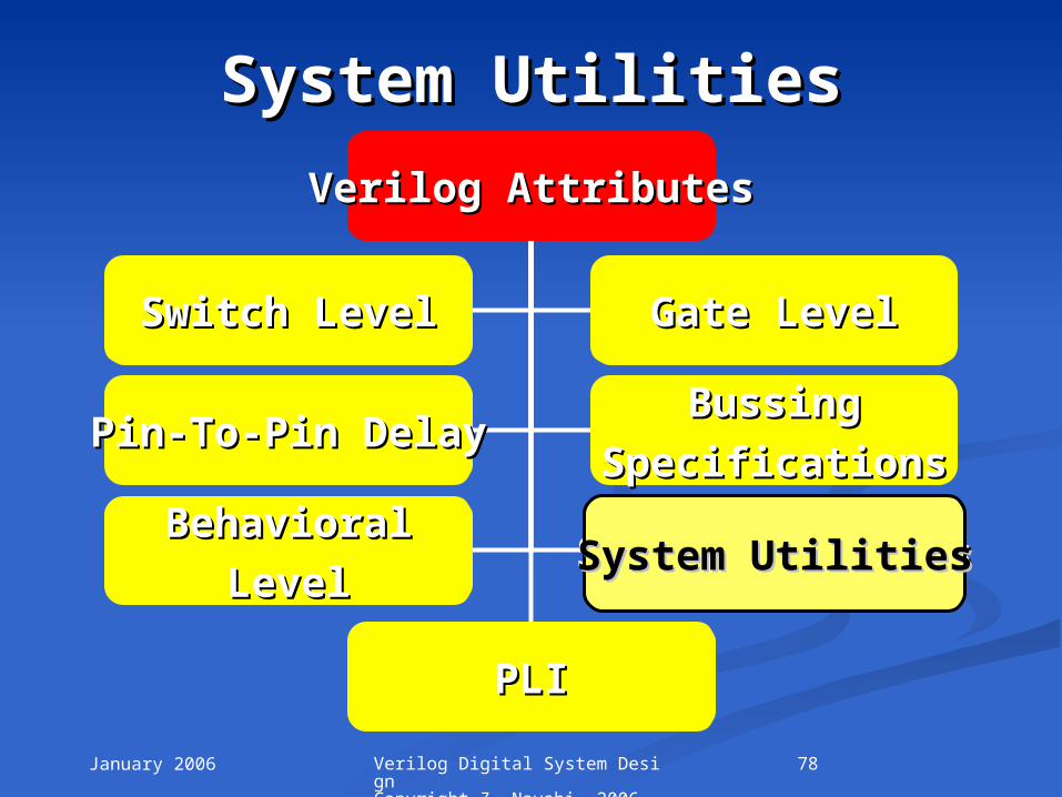
Verilog AttributesVerilog Attributes
PLIPLI
Switch LevelSwitch Level Gate LevelGate Level
Pin-To-Pin DelayPin-To-Pin DelayBussingBussing
SpecificationsSpecifications
BehavioralBehavioral
LevelLevelSystem UtilitiesSystem Utilities
Verilog AttributesVerilog Attributes
January 2006 68Verilog Digital System Design Copyright Z. Navabi, 2006
Verilog AttributesVerilog Attributes
PLIPLI
Switch LevelSwitch Level Gate LevelGate Level
Pin-To-Pin DelayPin-To-Pin DelayBussingBussing
SpecificationsSpecifications
BehavioralBehavioral
LevelLevelSystem UtilitiesSystem Utilities
Switch LevelSwitch Level
Switch LevelSwitch Level
January 2006 69Verilog Digital System Design Copyright Z. Navabi, 2006
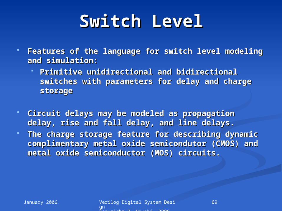
Switch LevelSwitch Level Features of the language for switch level modeling Features of the language for switch level modeling
and simulation:and simulation: Primitive unidirectional and bidirectional switches Primitive unidirectional and bidirectional switches
with parameters for delay and charge storagewith parameters for delay and charge storage
Circuit delays may be modeled as propagation delay, Circuit delays may be modeled as propagation delay, rise and fall delay, and line delays. rise and fall delay, and line delays.
The charge storage feature for describing dynamic The charge storage feature for describing dynamic complimentary metal oxide semicondutor (CMOS) complimentary metal oxide semicondutor (CMOS) and metal oxide semiconductor (MOS) circuits.and metal oxide semiconductor (MOS) circuits.
January 2006 70Verilog Digital System Design Copyright Z. Navabi, 2006
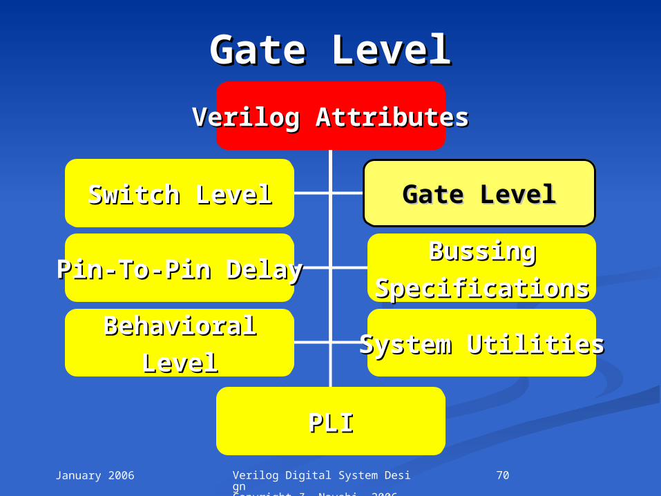
Verilog AttributesVerilog Attributes
PLIPLI
Switch LevelSwitch Level Gate LevelGate Level
Pin-To-Pin DelayPin-To-Pin DelayBussingBussing
SpecificationsSpecifications
BehavioralBehavioral
LevelLevelSystem UtilitiesSystem Utilities
Gate LevelGate Level
Gate LevelGate Level

January 2006 71Verilog Digital System Design Copyright Z. Navabi, 2006
Gate LevelGate Level Gate level primitives with predefined parameters Gate level primitives with predefined parameters
provide a convenient platform for:provide a convenient platform for: netlist representation netlist representation gate level simulation. gate level simulation.
For more detailed and special purpose gate For more detailed and special purpose gate simulations:simulations: Gate components defined at the behavioral level. Gate components defined at the behavioral level.
Verilog provides utilities for defining primitives with Verilog provides utilities for defining primitives with special functionalities:special functionalities: A simple 4-value logic system used for signal values A simple 4-value logic system used for signal values 16 levels of strength in addition to the four values 16 levels of strength in addition to the four values
for more accurate logic modelingfor more accurate logic modeling

January 2006 72Verilog Digital System Design Copyright Z. Navabi, 2006
Verilog AttributesVerilog Attributes
PLIPLI
Switch LevelSwitch Level Gate LevelGate Level
Pin-To-Pin DelayPin-To-Pin DelayBussingBussing
SpecificationsSpecifications
BehavioralBehavioral
LevelLevelSystem UtilitiesSystem Utilities
Pin-To-Pin DelayPin-To-Pin Delay
Pin-To-Pin DelayPin-To-Pin Delay

January 2006 73Verilog Digital System Design Copyright Z. Navabi, 2006
Pin-To-Pin DelayPin-To-Pin Delay
Verilog provides a utility for timing specification of Verilog provides a utility for timing specification of components at the input/output level:components at the input/output level: Can be used for back annotation of timing Can be used for back annotation of timing
information in original predesigned descriptionsinformation in original predesigned descriptions Enables modelers to finetune timing behavior of Enables modelers to finetune timing behavior of
their models based on physical implementationstheir models based on physical implementations
January 2006 74Verilog Digital System Design Copyright Z. Navabi, 2006
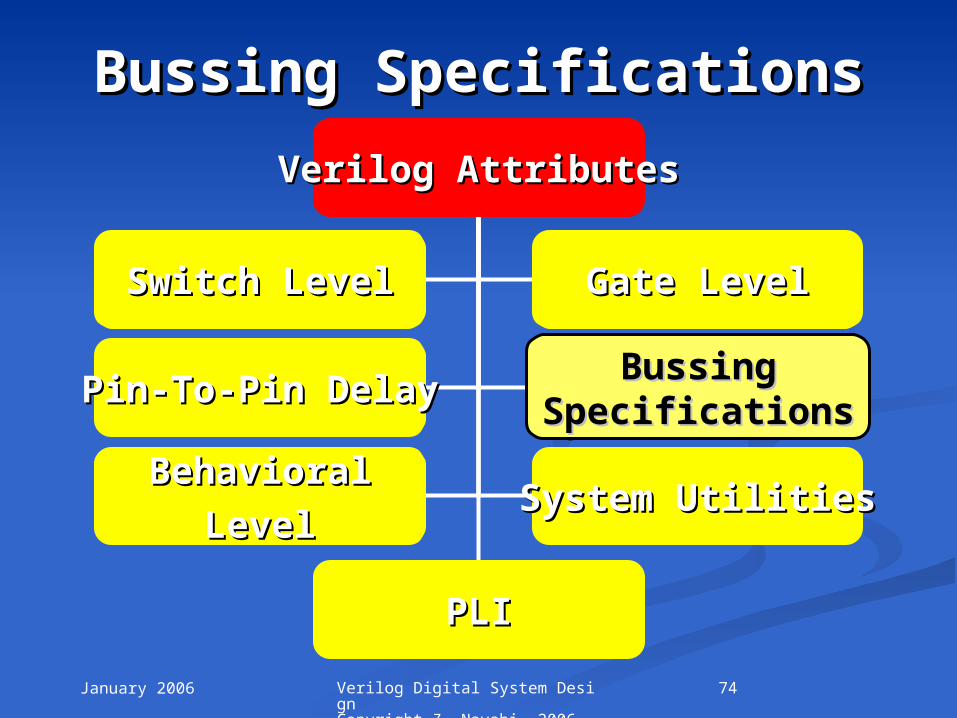
Verilog AttributesVerilog Attributes
PLIPLI
Switch LevelSwitch Level Gate LevelGate Level
Pin-To-Pin DelayPin-To-Pin DelayBussingBussing
SpecificationsSpecifications
BehavioralBehavioral
LevelLevelSystem UtilitiesSystem Utilities
Bussing SpecificationsBussing Specifications
BussingBussingSpecificationsSpecifications
January 2006 75Verilog Digital System Design Copyright Z. Navabi, 2006
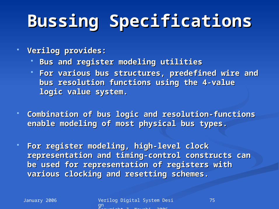
Bussing SpecificationsBussing Specifications Verilog provides:Verilog provides:
Bus and register modeling utilitiesBus and register modeling utilities For various bus structures, predefined wire and For various bus structures, predefined wire and
bus resolution functions using the 4-value logic bus resolution functions using the 4-value logic value system. value system.
Combination of bus logic and resolution-functions Combination of bus logic and resolution-functions enable modeling of most physical bus types. enable modeling of most physical bus types.
For register modeling, high-level clock For register modeling, high-level clock representation and timing-control constructs can be representation and timing-control constructs can be used for representation of registers with various used for representation of registers with various clocking and resetting schemes.clocking and resetting schemes.
January 2006 76Verilog Digital System Design Copyright Z. Navabi, 2006
Verilog AttributesVerilog Attributes
PLIPLI
Switch LevelSwitch Level Gate LevelGate Level
Pin-To-Pin DelayPin-To-Pin DelayBussingBussing
SpecificationsSpecifications
BehavioralBehavioral
LevelLevelSystem UtilitiesSystem Utilities
Behavioral LevelBehavioral Level
BehavioralBehavioralLevelLevel
January 2006 77Verilog Digital System Design Copyright Z. Navabi, 2006
Behavioral LevelBehavioral Level
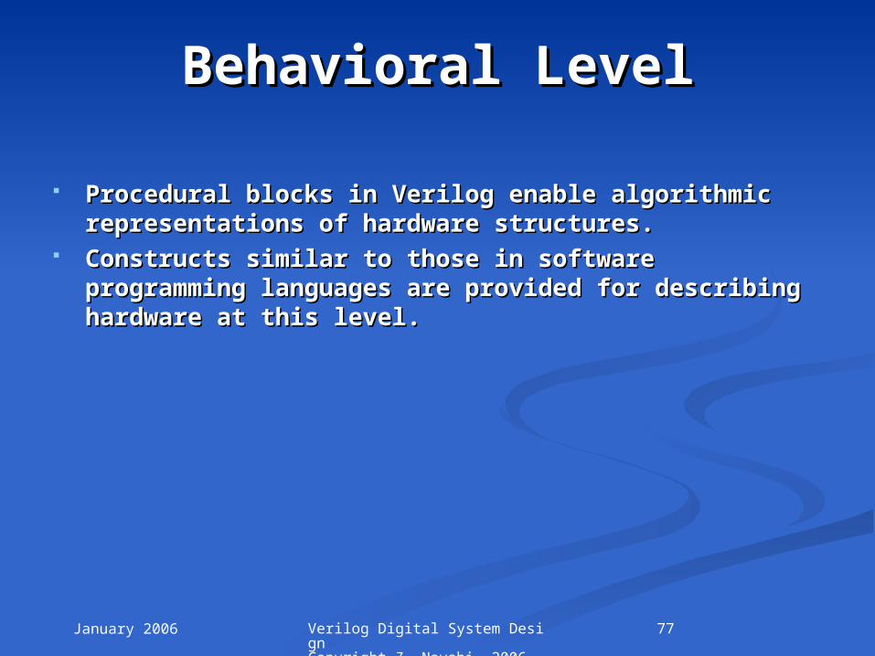
Procedural blocks in Verilog enable algorithmic Procedural blocks in Verilog enable algorithmic representations of hardware structures. representations of hardware structures.
Constructs similar to those in software programming Constructs similar to those in software programming languages are provided for describing hardware at languages are provided for describing hardware at this level.this level.
January 2006 78Verilog Digital System Design Copyright Z. Navabi, 2006
Verilog AttributesVerilog Attributes
PLIPLI
Switch LevelSwitch Level Gate LevelGate Level
Pin-To-Pin DelayPin-To-Pin DelayBussingBussing
SpecificationsSpecifications
BehavioralBehavioral
LevelLevelSystem UtilitiesSystem Utilities
System UtilitiesSystem Utilities
System UtilitiesSystem Utilities
January 2006 79Verilog Digital System Design Copyright Z. Navabi, 2006
System UtilitiesSystem Utilities System tasks in Verilog provide designers with tools for :System tasks in Verilog provide designers with tools for :
Testbench generationTestbench generation File access for read and writeFile access for read and write Data handlingData handling Data generationData generation Special hardware modeling. Special hardware modeling.
System utilities for reading memory and programmable System utilities for reading memory and programmable logic array (PLA) images provide convenient ways of logic array (PLA) images provide convenient ways of modeling these components.modeling these components.
Verilog display and I/O tasks can be used to handle all Verilog display and I/O tasks can be used to handle all inputs and outputs for data application and simulation. inputs and outputs for data application and simulation.
Verilog allows random access to files for read and write Verilog allows random access to files for read and write operations.operations.

January 2006 80Verilog Digital System Design Copyright Z. Navabi, 2006
Verilog AttributesVerilog Attributes
PLIPLI
Switch LevelSwitch Level Gate LevelGate Level
Pin-To-Pin DelayPin-To-Pin DelayBussingBussing
SpecificationsSpecifications
BehavioralBehavioral
LevelLevelSystem UtilitiesSystem Utilities
PLIPLI
PLIPLI
January 2006 81Verilog Digital System Design Copyright Z. Navabi, 2006
The Verilog LanguageThe Verilog Language
VerilogVerilog
HDLHDL
VerilogVerilog
EvolutionEvolutionVerilogVerilog
AttributesAttributesThe VerilogThe Verilog
LanguageLanguageThe VerilogThe VerilogLanguageLanguage
January 2006 82Verilog Digital System Design Copyright Z. Navabi, 2006
The Verilog LanguageThe Verilog Language The Verilog HDL satisfies all requirements for design The Verilog HDL satisfies all requirements for design
and synthesis of digital systems:and synthesis of digital systems:
Supports hierarchical description of hardware Supports hierarchical description of hardware from system to gate or even switch level. from system to gate or even switch level.
Has strong support at all levels for timing Has strong support at all levels for timing specification and violation detection. specification and violation detection.
Timing and concurrency required for hardware Timing and concurrency required for hardware modeling are specially emphasized in it.modeling are specially emphasized in it.
A hardware component is described by the A hardware component is described by the module_declaration module_declaration language construct in it. language construct in it.
January 2006 83Verilog Digital System Design Copyright Z. Navabi, 2006
The Verilog LanguageThe Verilog Language The Verilog HDL satisfies all requirements for design The Verilog HDL satisfies all requirements for design
and synthesis of digital systems (Continued):and synthesis of digital systems (Continued):
Description of a module specifies a component’s Description of a module specifies a component’s input and output list as well as internal input and output list as well as internal component busses and registers within a component busses and registers within a modulemodule, , concurrent assignments, component concurrent assignments, component instantiations, and procedural blocks can be used instantiations, and procedural blocks can be used to describe a hardware component.to describe a hardware component.
Several modules can hierarchically be instantiated Several modules can hierarchically be instantiated to form other hardware structures. to form other hardware structures.
Many Verilog tools and environments exist that Many Verilog tools and environments exist that provide simulation, fault simulation, formal provide simulation, fault simulation, formal verification, and synthesis. verification, and synthesis.
Simulation environments provide graphical front-Simulation environments provide graphical front-end programs and waveform editing and display end programs and waveform editing and display tools. tools.
Synthesis tools are based on a subset of Verilog. Synthesis tools are based on a subset of Verilog.
January 2006 84Verilog Digital System Design Copyright Z. Navabi, 2006
SummarySummary
This chapter presented:This chapter presented: An overview of mechanisms, tools, and processes An overview of mechanisms, tools, and processes
used for taking a design from the design stage to a used for taking a design from the design stage to a hardware implementationhardware implementation
The history of Verilog evolutionThe history of Verilog evolution With this standard HDL, the efforts of tool With this standard HDL, the efforts of tool
developers, researchers, and software vendors developers, researchers, and software vendors have become more focused, resulting in better have become more focused, resulting in better tools and more uniform environments. tools and more uniform environments.