0-30V / 5A DIGITAL POWER SUPPLY WITH COMPUTER CONTROL by Önder Sünetci B.S., in Electronics Engineering, İstanbul University, 2002 Submitted to the Institute for Graduate Studies in Science and Engineering in partial fulfillment of the requirements for the degree of Master of Science Graduate Program in Electrical and Electronics Engineering Boğaziçi University 2010

Welcome message from author
This document is posted to help you gain knowledge. Please leave a comment to let me know what you think about it! Share it to your friends and learn new things together.
Transcript
0-30V / 5A DIGITAL POWER SUPPLY
WITH COMPUTER CONTROL
by
Önder Sünetci
B.S., in Electronics Engineering, İstanbul University, 2002
Submitted to the Institute for Graduate Studies in
Science and Engineering in partial fulfillment of
the requirements for the degree of
Master of Science
Graduate Program in Electrical and Electronics Engineering
Boğaziçi University
2010

ii
0-30V / 5A DIGITAL POWER SUPPLY
WITH COMPUTER CONTROL
APPROVED BY:
Prof. Yasemin Kahya ……………….
(Thesis Supervisor)
Prof. Ömer Cerid ……………….
(Thesis Co-Advisor)
Prof. Günhan Dündar ……………….
Assoc Prof. Özcan Gülçür ……………….
DATE OF APPROVAL: ……………….

iii
ACKNOWLEDGEMENTS
I am very grateful to my thesis supervisor Prof. Yasemin Kahya for encouraging and
motivating me, trusting me and guiding me during my thesis. Without her valuable support
it would have been very hard for me to complete my study.
I also want to extend my great thanks to Prof. Ömer Cerid for guiding me at the hard
breakpoints and giving very important suggestions.
I would like to thank Prof. Günhan Dündar and Assoc Prof. Özcan Gülçür for their
interest and evaluation of my thesis and being jury members.
I would like to thank Gökhan Yıldız, Yusuf Yıldırım, Övünç Doruk İzgen, İlkin
Tacan, Çağatay Büyüktopçu, Selami Çevik, Erhan Gündoğan and Eren Uyar from Arçelik
Company for their supports.
Finally, I would like to thank my wife, my mother and my father for their invaluable
support and motivation at the important milestones of this thesis. I would also like to thank
my little son Yunus Emre, for being a reason of extra motivation although he does not
know.

iv
ABSTRACT
0-30V / 5A DIGITAL POWER SUPPLY
WITH COMPUTER CONTROL
Most of the electronic circuits require a DC power supply to operate. There are many
designs and topologies covering different properties and specifications for DC power
supplies.
The voltage and current range and accuracy, power capacity and quality, failure
protections, isolations, robustness and reliability, power efficiency, size and ease of usage
are some of the most important characteristics of power supplies.
A DC power supply with the parameters given in the following sections is designed
and realized for the fulfillment of the Master of Science thesis. The criteria for making
decisions on the design parameters were range, isolations and ease of use. The range is
proposed to be 30VDC and 5A output. The isolation is realized both between the mains
and the device and between the device and PC that, when connected, controls it. For the
ease of use, a 4x4 keypad to enter data and a 2x20 character LCD to monitor data are used.

v
ÖZET
BİLGİSAYAR DENETİMLİ
0-30V / 5A SAYISAL GÜÇ KAYNAĞI
Elektronik devrelerin çoğu işlevlerini yerine getirebilmek için doğru akım
kaynaklarına gereksinim duyar. Birçok farklı özellik ve spesifikasyonlarda çok çeşitli
tasarım ve topolojiye sahip doğru akım kaynakları mevcuttur.
Gerilim ve akım aralığı ve doğruluğu, güç kapasitesi ve kalitesi, hata korumaları,
yalıtımlar, sağlamlık ve güvenilirlik, güç verimliliği, boyutlar ve kullanım kolaylığı güç
kaynaklarının en önemli karakteristiklerinden bazılarıdır.
Bu yüksek lisans tezinin yerine getirilmesi için, takip eden bölümlerde belirtilen
parametrelere sahip bir doğru akım güç kaynağı tasarlanıp gerçekleştirilmiştir. Tasarım
parametrelerine karar vermedeki ölçütler aralık, yalıtım ve kullanım kolaylığı olmuştur.
Aralık 30VDC’ye ve 5A’e kadar çıkış verebilecek şekilde önerilmiştir. Hem şebeke ile
cihaz arasında hem de bağlandığında cihazı kontrol eden bilgisayar ile cihaz arasında
yalıtım bulunmaktadır. Kullanım kolaylığı için veri girmede kullanmak üzere 4x4
tuştakımı ve veri görüntülemede kullanmak üzere 2x20 karakter LCD kullanılmıştır.
vi
TABLE OF CONTENTS
ACKNOWLEDGEMENTS............................................................................................... iii
ABSTRACT....................................................................................................................... iv
ÖZET ................................................................................................................................ v
LIST OF FIGURES ........................................................................................................... viii
LIST OF TABLES............................................................................................................ x
1. INTRODUCTION ....................................................................................................... 1
1.1. Linear Power Supplies .......................................................................................... 2
1.2. Switch Mode Power Supplies ............................................................................... 3
1.2.1. The Isolated Fly-back Converter................................................................. 3
1.2.2. Forward Converter ...................................................................................... 4
1.2.3. Boost Converter .......................................................................................... 4
2. DESIGN METHODOLOGY....................................................................................... 5
2.1. Block Diagram Drawing ....................................................................................... 5
2.2. Regulator Transistor Selection.............................................................................. 6
2.3. Paralleling Transistors for Current Sharing .......................................................... 6
2.4. Determination of the Emitter Resistance Values .................................................. 7
2.4.1. The User Interface....................................................................................... 9
2.4.2. The Overall Control Unit of the Power Supply ......................................... 10
2.4.1. The Overall Power Unit of the Power Supply ........................................... 11
2.4.2. Measuring the Output Voltage................................................................... 12
2.4.3. Measuring the Output Current ................................................................... 14
2.4.4. Measuring the Heatsink Temperature ........................................................ 16
vii
2.4.5. Setting (Regulating) the Output Voltage ................................................... 19
2.5. Microcontroller Decision and Connections ......................................................... 21
2.6. Keypad Interface .................................................................................................. 22
2.7. Computer Interface .............................................................................................. 23
2.8. LCD Interface ...................................................................................................... 24
2.9. Microcontroller Programming ............................................................................. 25
2.10. Buzzer Circuit .................................................................................................... 25
2.11. Thermal (Heatsink) Considerations ................................................................... 26
2.12. Output Overcurrent Protection........................................................................... 30
2.13. The PCB Design................................................................................................. 30
3. SOFTWARE ............................................................................................................... 33
3.1. The Embedded Code............................................................................................ 33
3.2. The Computer Interface Program ........................................................................ 34
4. RESULTS ................................................................................................................... 35
4.1. Efficiency ............................................................................................................. 35
5. CONCLUSION & FUTURE WORK ......................................................................... 39
APPENDIX A: DATASHEETS...................................................................................... 42
A.1. TIP142 Datasheet..................................................................................................... 42
A.2. AD5235 Datasheet (Summary)................................................................................ 45
A.3. ATMEGA16 Datasheet (Summary) ........................................................................ 48
A.4. WH2002A-TMI-ET LCD Datasheet (Summary) .................................................... 52
A.5. GBPC2510 Bridge Rectifier Datasheet (Summary) ................................................ 56
A.6. B57703M0103A017 NTC Datasheet (Summary) ................................................... 60
APPENDIX B: EMBEDDED CODE.............................................................................. 62
REFERENCES ....................................................................................................................77
viii
LIST OF FIGURES
Figure 1.1. Power supply parameter definitions [3] ...................................................... 2
Figure 1.2. Basic linear power supply topology ............................................................... 2
Figure 1.3. Flyback converter ........................................................................................... 3
Figure 1.4. Forward converter .......................................................................................... 4
Figure 1.5. Boost converter............................................................................................... 4
Figure 2.1. Block diagram of the power supply ............................................................... 5
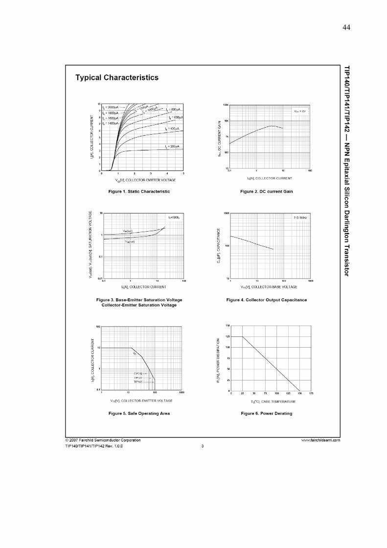
Figure 2.2. TIP142 safe operating area (VCE vs. IC) [4] ................................................... 6
Figure 2.3. TIP142 power derating (TC vs. PC) [4]........................................................... 7
Figure 2.4. Paralleling transistors [5]................................................................................ 9
Figure 2.5. The schematic of the control unit of the power supply unit ........................... 10
Figure 2.6. The schematic of the power unit of the power supply unit ............................ 11
Figure 2.7. Output voltage measurement circuit............................................................... 12
Figure 2.8. Output current shunt resistor .......................................................................... 14
Figure 2.9. Output current measurement circuit ............................................................... 14
Figure 2.10. Heatsink temperature measurement circuit .................................................. 16
Figure 2.11. AD5235 dual digital potentiometer connections.......................................... 19
Figure 2.12. The voltage setting block ............................................................................. 20
Figure 2.13. The microcontroller connections.................................................................. 22
Figure 2.14. The 4x4 keypad and functions...................................................................... 22
Figure 2.15. The keypad connections to the microcontroller ........................................... 23
Figure 2.16. The communication connections with the microcontroller .......................... 23
Figure 2.17. The LCD connections................................................................................... 24
ix
Figure 2.18. The ISP10 programming connector ............................................................. 25
Figure 2.19. The Buzzer Circuit ....................................................................................... 25
Figure 2.20. The power regulation part of the design....................................................... 26
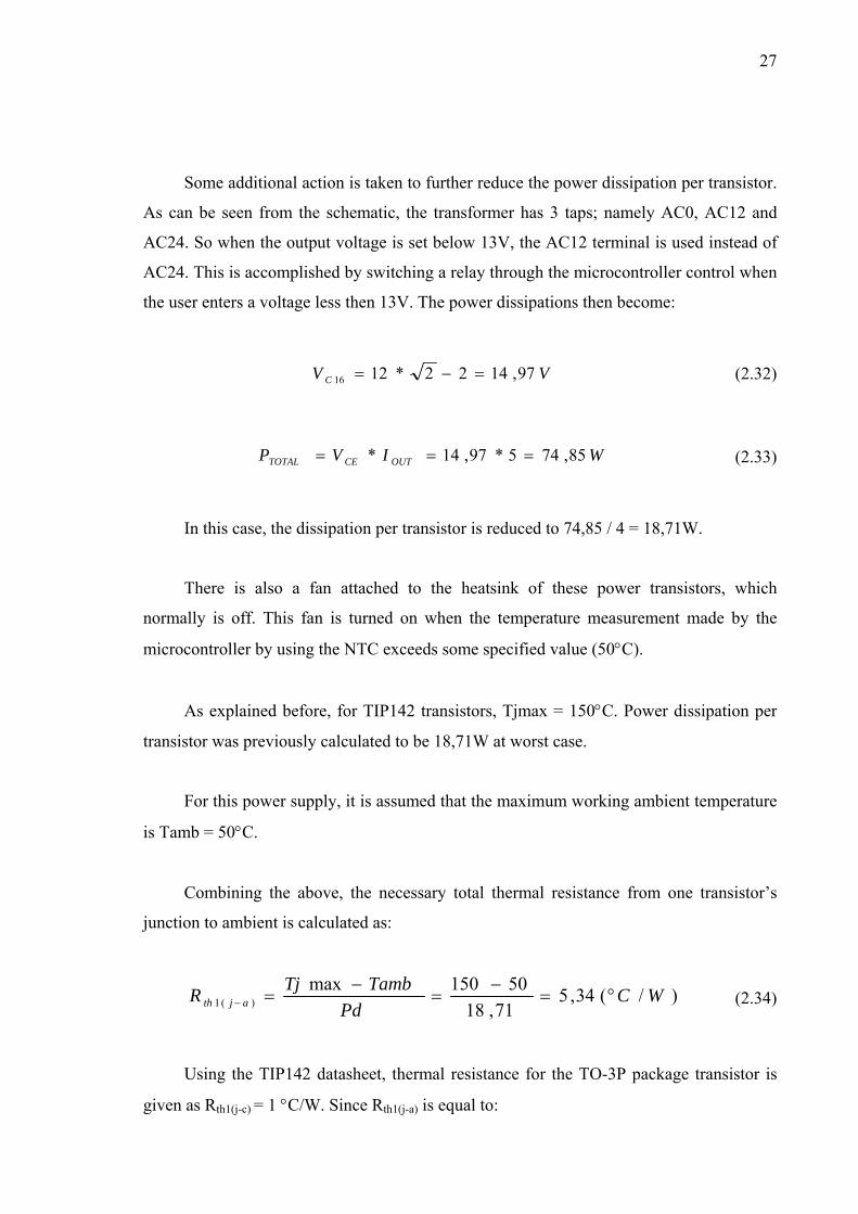
Figure 2.21. The heatsink simulation showing the power dissipations ............................ 28
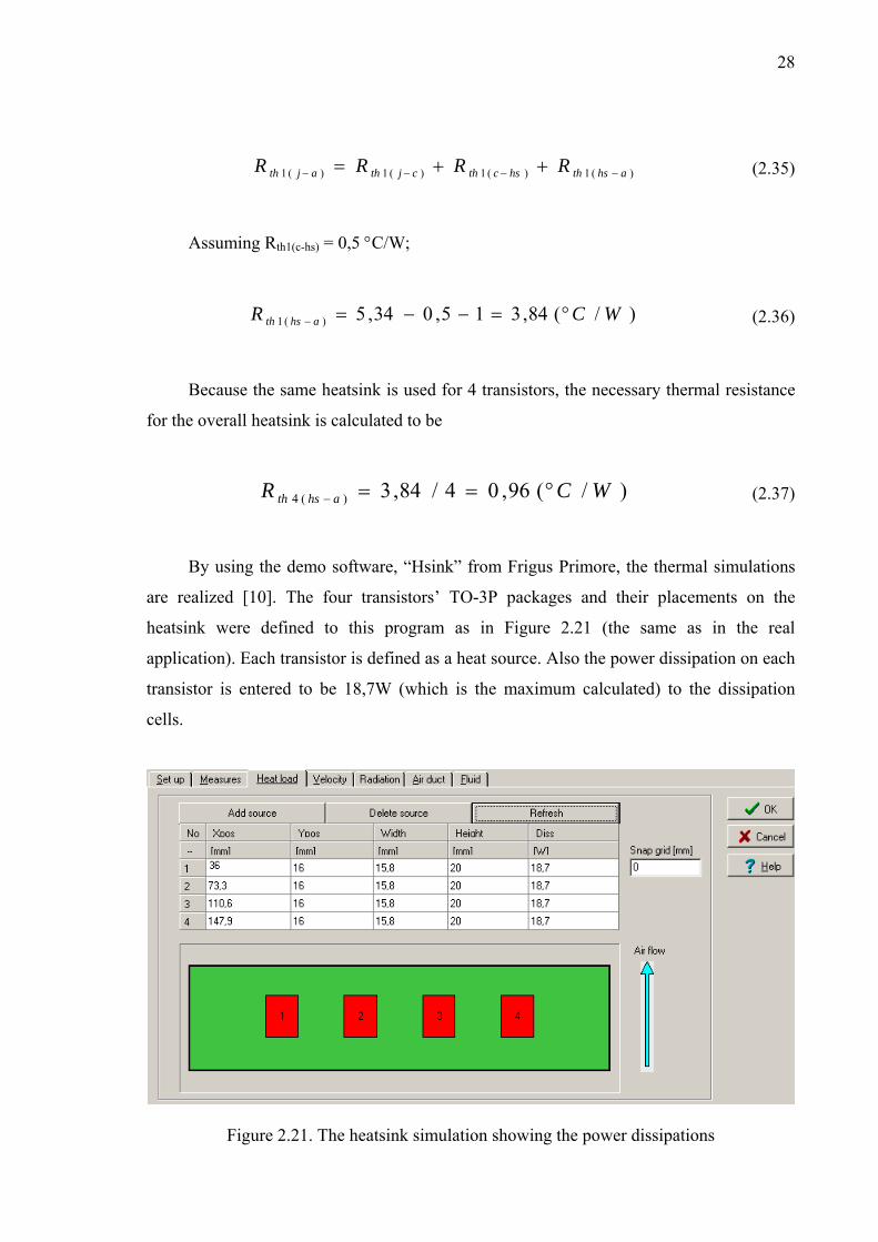
Figure 2.22. The heatsink simulation showing the heatsink dimensions.......................... 29
Figure 2.23. The 3D model for the heatsink and the transistors as heat sources.............. 29
Figure 2.24. The result of the heatsink simulation showing the heat distribution............ 30
Figure 2.25. The PCB design of the power supply........................................................... 31
Figure 2.26. The top placement of the PCB of the power supply..................................... 31
Figure 2.27. The top layer of the PCB of the power supply ............................................. 32
Figure 2.28. The bottom layer of the PCB of the power supply....................................... 32
Figure 3.1. The programming screen of the programmer................................................. 33
Figure 3.2. Computer control interface of the power supply............................................ 34
Figure 4.1. The completed power supply ......................................................................... 36
Figure 4.2. The power supply from various angles .......................................................... 37
Figure 4.3. The inside of the power supply box and testing............................................. 38
Figure 4.4. The power supply testing and computer connection ...................................... 38
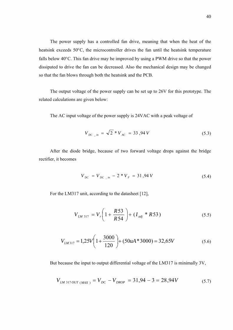
Figure 5.1. Digital potentiometer part .............................................................................. 41
x
LIST OF TABLES
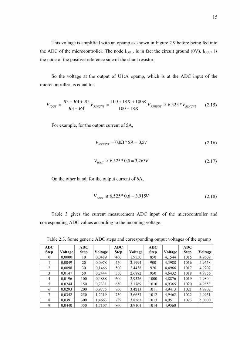
Table 2.1. Some generic ADC steps and corresponding voltages .................................... 13
Table 2.2. Corresponding output voltages to ADC steps of Table 1 ................................ 13
Table 2.3. Some generic ADC steps and corresponding output voltages of the opamp... 15
Table 2.4. The voltages on the NTC and corresponding ADC values and temperatures . 18
Table 4.1. Digital power supply efficiency calculator...................................................... 35
Table 4.2. Efficiency of the power supply for various output voltages and currents ....... 36
1
1. INTRODUCTION
All the electronic devices which are used in everyday life require some kind of
energy to operate. The kind of energy can be electrical, but it can also be mechanical,
chemical (gasoline, batteries, oil, natural gas, wood etc.), heat (thermal, steam etc.), kinetic
(sound, wind etc.), magnetic etc as well [1].
As for the most of the electronic devices require electrical power, especially DC
power, there are many kinds of DC power supplies designed for different purposes. Most
of these devices require not only DC voltage but voltage that is also well filtered and
regulated.
There are three types of electronic power conversion devices which are classified as
follows according to their input and output voltages: 1) DC/DC converter; 2) AC/DC
power supply; 3) DC/AC inverter. Each has its own area of use but the first two are the
most commonly used [2].
A power supply converting AC line voltage to DC power must perform the following
functions at high efficiency and at low cost:
1. Rectification: Convert the incoming AC line voltage to DC voltage.
2. Voltage transformation: Supply the correct DC voltage level(s).
3. Filtering: Smooth the ripple of the rectified voltage.
4. Regulation: Control the output voltage level to a constant value irrespective of
line, load and temperature changes.
5. Isolation: Separate electrically the output from the input voltage source.
2
6. Protection: Prevent damaging voltage surges from reaching the output; provide
back-up power or shut down during a brown-out.
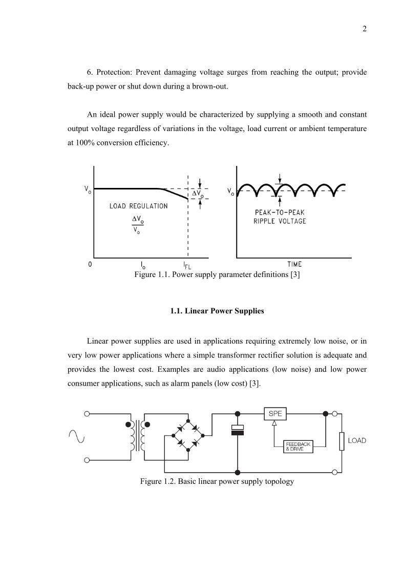
An ideal power supply would be characterized by supplying a smooth and constant
output voltage regardless of variations in the voltage, load current or ambient temperature
at 100% conversion efficiency.
Figure 1.1. Power supply parameter definitions [3]
1.1. Linear Power Supplies
Linear power supplies are used in applications requiring extremely low noise, or in
very low power applications where a simple transformer rectifier solution is adequate and
provides the lowest cost. Examples are audio applications (low noise) and low power
consumer applications, such as alarm panels (low cost) [3].
Figure 1.2. Basic linear power supply topology
3
The 50/60Hz mains transformer reduces the voltage to a usable low level, the
secondary AC voltage is peak-rectified and a series pass element (SPE) is employed to
provide the necessary regulation. The benefits of this solution are low noise, reliability and
low cost. On the downside, these units are large, heavy and inefficient with a limited input
voltage range.
1.2. Switch Mode Power Supplies
The use of switch mode topologies has reduced the size and improved the efficiency
of power supplies by increasing the frequency of operation, reducing the physical size of
transformers, inductors and capacitors, and utilizing an ‘on or off’ pulse width modulated
(PWM) switching element to increase efficiency. The compromises in adopting this
technique are increased ripple and noise on the output DC supply and the creation of both
conducted and radiated EMI, which have to be managed.
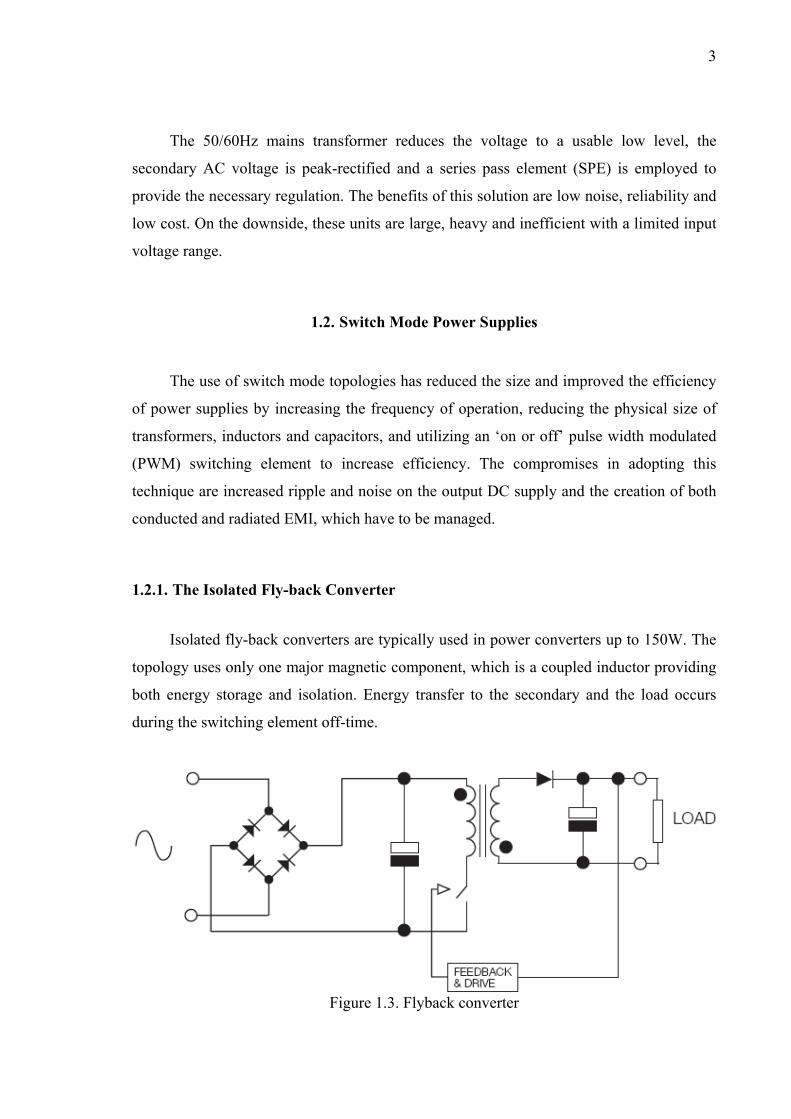
1.2.1. The Isolated Fly-back Converter
Isolated fly-back converters are typically used in power converters up to 150W. The
topology uses only one major magnetic component, which is a coupled inductor providing
both energy storage and isolation. Energy transfer to the secondary and the load occurs
during the switching element off-time.
Figure 1.3. Flyback converter
4
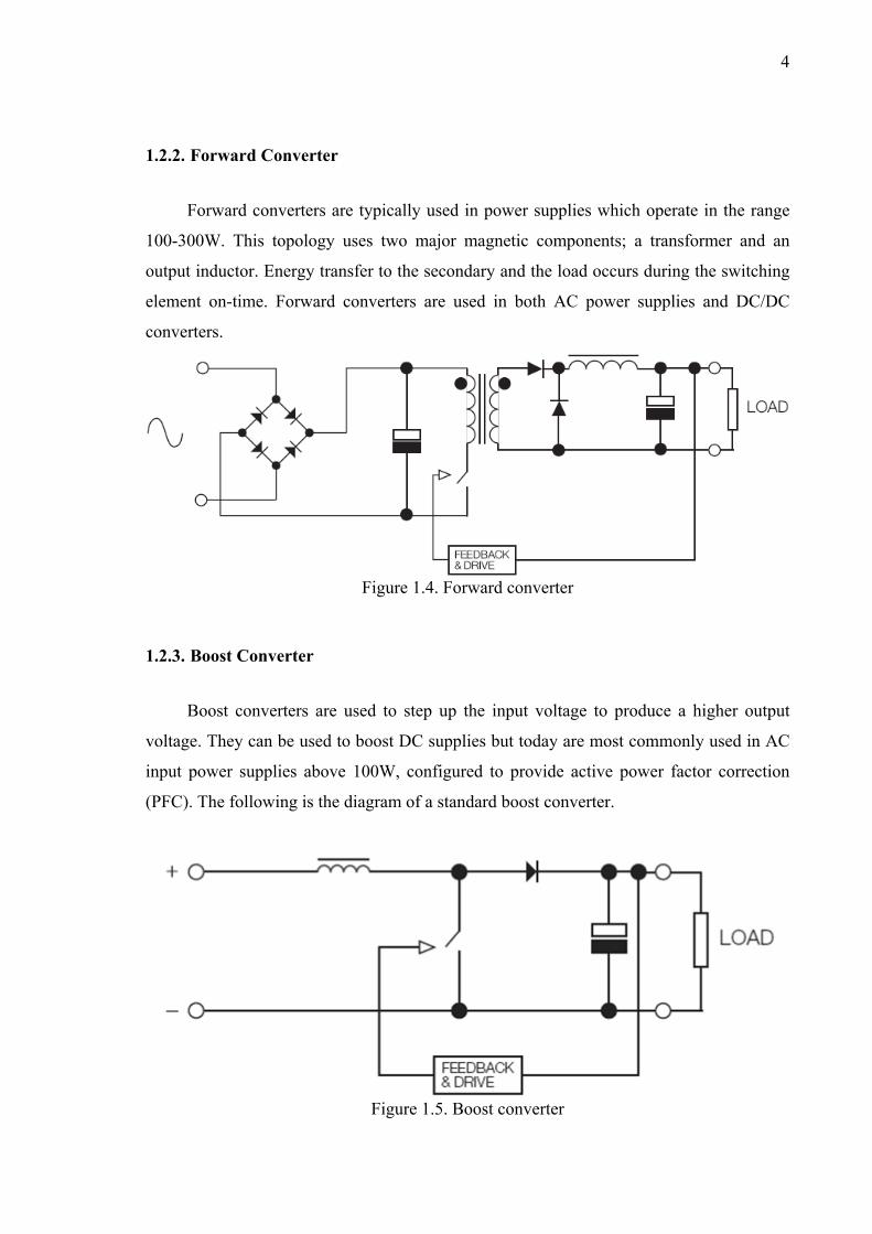
1.2.2. Forward Converter
Forward converters are typically used in power supplies which operate in the range
100-300W. This topology uses two major magnetic components; a transformer and an
output inductor. Energy transfer to the secondary and the load occurs during the switching
element on-time. Forward converters are used in both AC power supplies and DC/DC
converters.
Figure 1.4. Forward converter
1.2.3. Boost Converter
Boost converters are used to step up the input voltage to produce a higher output
voltage. They can be used to boost DC supplies but today are most commonly used in AC
input power supplies above 100W, configured to provide active power factor correction
(PFC). The following is the diagram of a standard boost converter.
Figure 1.5. Boost converter
5
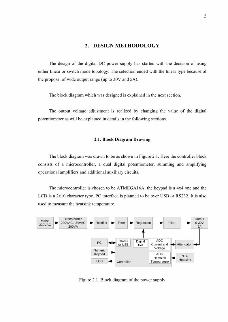
2. DESIGN METHODOLOGY
The design of the digital DC power supply has started with the decision of using
either linear or switch mode topology. The selection ended with the linear type because of
the proposal of wide output range (up to 30V and 5A).
The block diagram which was designed is explained in the next section.
The output voltage adjustment is realized by changing the value of the digital
potentiometer as will be explained in details in the following sections.
2.1. Block Diagram Drawing
The block diagram was drawn to be as shown in Figure 2.1. Here the controller block
consists of a microcontroller, a dual digital potentiometer, summing and amplifying
operational amplifiers and additional auxiliary circuits.
The microcontroller is chosen to be ATMEGA16A, the keypad is a 4x4 one and the
LCD is a 2x10 character type. PC interface is planned to be over USB or RS232. It is also
used to measure the heatsink temperature.
Figure 2.1. Block diagram of the power supply
Mains220VAC
Transformer220VAC / 24VAC
200VARectifier Filter Regulation
Numeric Keypad
Output0-30V
5A
PC
Filter
Controller
RS232 or USB
Digital Pot
LCD
ADCCurrent and
VoltageAttenuator
ADCHeatsink
Temperature
NTC Heatsink
6
2.2. Regulator Transistor Selection
The regulator transistors are chosen to be 4 x TIP142 NPN array. This transistor is a
darlington type and has a minimum DC current gain of hFE = 1000 @ VCE = 4V, IC = 5A
according to the Fairchild datasheet [4]. Four transistors are connected in parallel for load
current sharing, which will be explained in next sections.
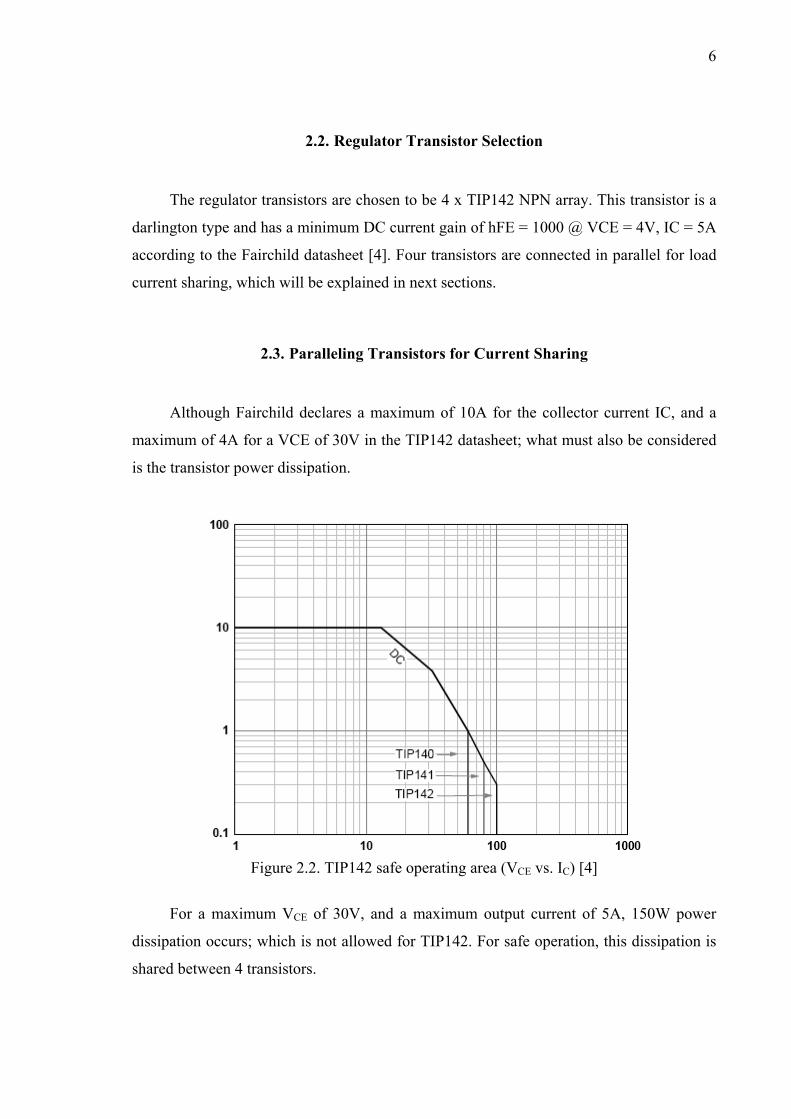
2.3. Paralleling Transistors for Current Sharing
Although Fairchild declares a maximum of 10A for the collector current IC, and a
maximum of 4A for a VCE of 30V in the TIP142 datasheet; what must also be considered
is the transistor power dissipation.
Figure 2.2. TIP142 safe operating area (VCE vs. IC) [4]
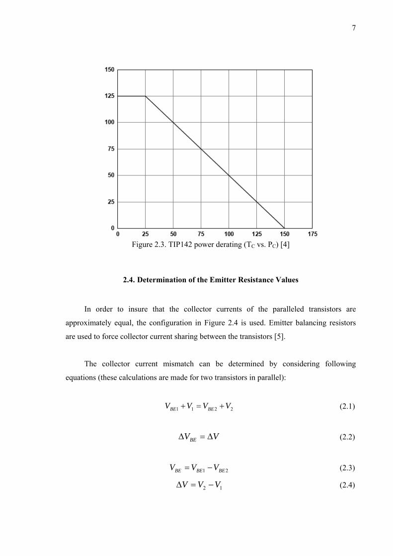
For a maximum VCE of 30V, and a maximum output current of 5A, 150W power
dissipation occurs; which is not allowed for TIP142. For safe operation, this dissipation is
shared between 4 transistors.
7
Figure 2.3. TIP142 power derating (TC vs. PC) [4]
2.4. Determination of the Emitter Resistance Values
In order to insure that the collector currents of the paralleled transistors are
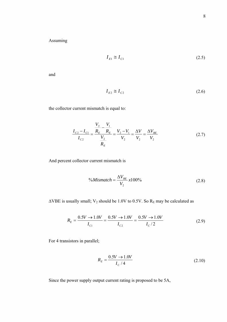
approximately equal, the configuration in Figure 2.4 is used. Emitter balancing resistors
are used to force collector current sharing between the transistors [5].
The collector current mismatch can be determined by considering following
equations (these calculations are made for two transistors in parallel):
2211 VVVV BEBE +=+ (2.1)
VVBE Δ=Δ (2.2)
21 BEBEBE VVV −= (2.3)
12 VVV −=Δ (2.4)
8
Assuming
11 CE II ≅ (2.5)
and
22 CE II ≅ (2.6)
the collector current mismatch is equal to:
222
12
2
12
2
12
VV
VV
VVV
RV
RV
RV
III BE
E
EE
C
CC Δ=
Δ=
−=
−=
− (2.7)
And percent collector current mismatch is
%100%2
xVVMismatch BEΔ
= (2.8)
ΔVBE is usually small; V2 should be 1.0V to 0.5V. So RE may be calculated as
2/0.15.00.15.00.15.0
21 CCCE I
VVI
VVI
VVR →=
→=
→= (2.9)
For 4 transistors in parallel;
4/0.15.0
CE I
VVR →= (2.10)
Since the power supply output current rating is proposed to be 5A,
9
Ω→Ω=→
= 8,04,04/5
0.15.0 VVRE (2.11)
The emitter resistors are chosen to be 0,47R / 2W.
Figure 2.4. Paralleling transistors [5]
2.4.1. The User Interface
The user interface is proposed to be simple. So a 4x4 keypad and a 2x20 LCD are
considered to be sufficient. The LCD is an easy to read, white over blue negative type [6].
A buzzer has been used to make hearable warnings. For the computer interface, a
USB/RS232 connector is placed on the power supply.
10
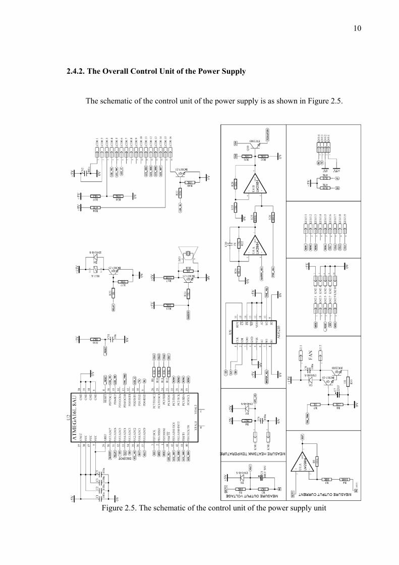
2.4.2. The Overall Control Unit of the Power Supply
The schematic of the control unit of the power supply is as shown in Figure 2.5.
Figure 2.5. The schematic of the control unit of the power supply unit
11
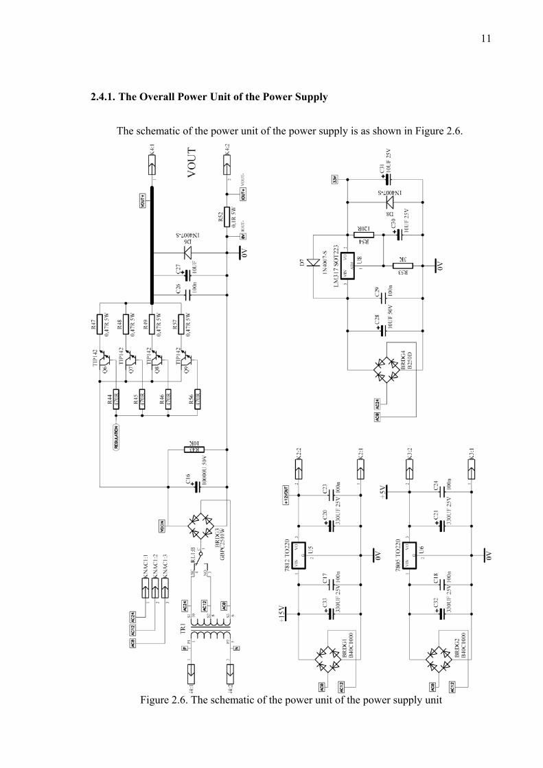
2.4.1. The Overall Power Unit of the Power Supply
The schematic of the power unit of the power supply is as shown in Figure 2.6.
Figure 2.6. The schematic of the power unit of the power supply unit
12
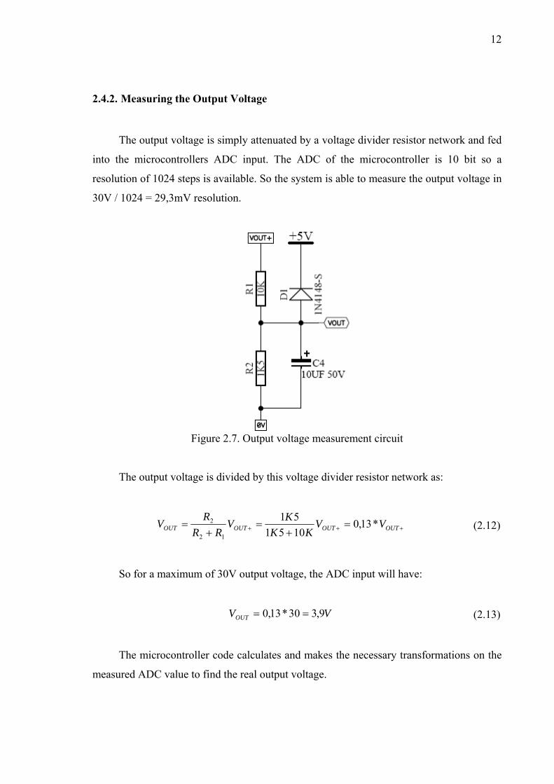
2.4.2. Measuring the Output Voltage
The output voltage is simply attenuated by a voltage divider resistor network and fed
into the microcontrollers ADC input. The ADC of the microcontroller is 10 bit so a
resolution of 1024 steps is available. So the system is able to measure the output voltage in
30V / 1024 = 29,3mV resolution.
Figure 2.7. Output voltage measurement circuit
The output voltage is divided by this voltage divider resistor network as:
+++ =+
=+
= OUTOUTOUTOUT VVKK
KVRR
RV *13,0105151
12
2 (2.12)
So for a maximum of 30V output voltage, the ADC input will have:
VVOUT 9,330*13,0 == (2.13)
The microcontroller code calculates and makes the necessary transformations on the
measured ADC value to find the real output voltage.
13
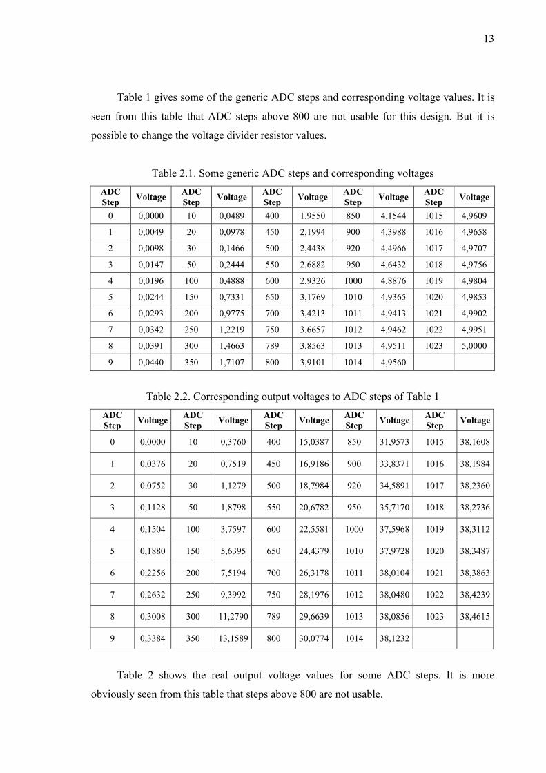
Table 1 gives some of the generic ADC steps and corresponding voltage values. It is
seen from this table that ADC steps above 800 are not usable for this design. But it is
possible to change the voltage divider resistor values.
Table 2.1. Some generic ADC steps and corresponding voltages ADC Step Voltage ADC
Step Voltage ADC Step Voltage ADC
Step Voltage ADC Step Voltage
0 0,0000 10 0,0489 400 1,9550 850 4,1544 1015 4,9609
1 0,0049 20 0,0978 450 2,1994 900 4,3988 1016 4,9658
2 0,0098 30 0,1466 500 2,4438 920 4,4966 1017 4,9707
3 0,0147 50 0,2444 550 2,6882 950 4,6432 1018 4,9756
4 0,0196 100 0,4888 600 2,9326 1000 4,8876 1019 4,9804
5 0,0244 150 0,7331 650 3,1769 1010 4,9365 1020 4,9853
6 0,0293 200 0,9775 700 3,4213 1011 4,9413 1021 4,9902
7 0,0342 250 1,2219 750 3,6657 1012 4,9462 1022 4,9951
8 0,0391 300 1,4663 789 3,8563 1013 4,9511 1023 5,0000
9 0,0440 350 1,7107 800 3,9101 1014 4,9560
Table 2.2. Corresponding output voltages to ADC steps of Table 1 ADC Step Voltage ADC
Step Voltage ADC Step Voltage ADC
Step Voltage ADC Step Voltage
0 0,0000 10 0,3760 400 15,0387 850 31,9573 1015 38,1608
1 0,0376 20 0,7519 450 16,9186 900 33,8371 1016 38,1984
2 0,0752 30 1,1279 500 18,7984 920 34,5891 1017 38,2360
3 0,1128 50 1,8798 550 20,6782 950 35,7170 1018 38,2736
4 0,1504 100 3,7597 600 22,5581 1000 37,5968 1019 38,3112
5 0,1880 150 5,6395 650 24,4379 1010 37,9728 1020 38,3487
6 0,2256 200 7,5194 700 26,3178 1011 38,0104 1021 38,3863
7 0,2632 250 9,3992 750 28,1976 1012 38,0480 1022 38,4239
8 0,3008 300 11,2790 789 29,6639 1013 38,0856 1023 38,4615
9 0,3384 350 13,1589 800 30,0774 1014 38,1232
Table 2 shows the real output voltage values for some ADC steps. It is more
obviously seen from this table that steps above 800 are not usable.
14
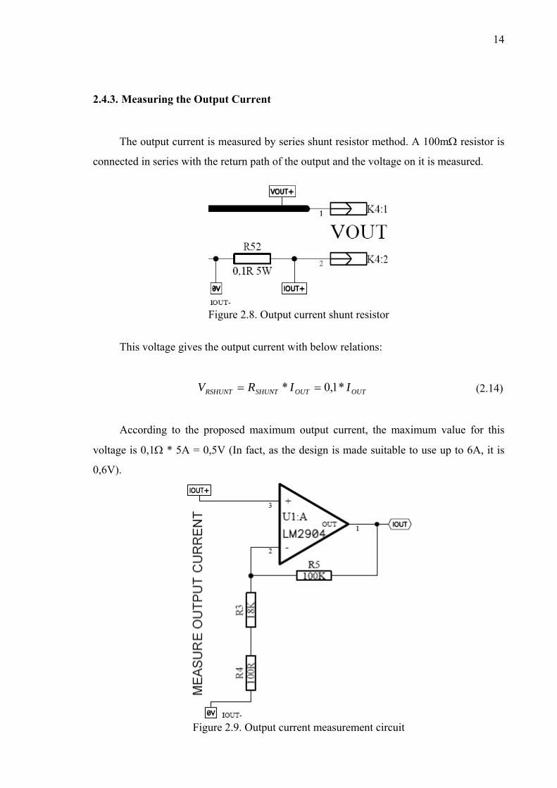
2.4.3. Measuring the Output Current
The output current is measured by series shunt resistor method. A 100mΩ resistor is
connected in series with the return path of the output and the voltage on it is measured.
Figure 2.8. Output current shunt resistor
This voltage gives the output current with below relations:
OUTOUTSHUNTRSHUNT IIRV *1,0* == (2.14)
According to the proposed maximum output current, the maximum value for this
voltage is 0,1Ω * 5A = 0,5V (In fact, as the design is made suitable to use up to 6A, it is
0,6V).
Figure 2.9. Output current measurement circuit
15
This voltage is amplified with an opamp as shown in Figure 2.9 before being fed into
the ADC of the microcontroller. The node IOUT- is in fact the circuit ground (0V). IOUT+ is
the node of the positive reference side of the shunt resistor.
So the voltage at the output of U1:A opamp, which is at the ADC input of the
microcontroller, is equal to:
RSHUNTRSHUNTRSHUNTIOUT VVK
KKVRR
RRRV *525,618100
1001810043
543≅
+++
=+++
= (2.15)
For example, for the output current of 5A,
VAVRSHUNT 5,05*1,0 =Ω= (2.16)
VVIOUT 263,35,0*525,6 =≅ (2.17)
On the other hand, for the output current of 6A,
VVIOUT 915,36,0*525,6 =≅ (2.18)
Table 3 gives the current measurement ADC input of the microcontroller and
corresponding ADC values according to the incoming voltage.
Table 2.3. Some generic ADC steps and corresponding output voltages of the opamp ADC Step Voltage
ADC Step Voltage
ADC Step Voltage
ADC Step Voltage
ADC Step Voltage
0 0,0000 10 0,0489 400 1,9550 850 4,1544 1015 4,9609 1 0,0049 20 0,0978 450 2,1994 900 4,3988 1016 4,9658 2 0,0098 30 0,1466 500 2,4438 920 4,4966 1017 4,9707 3 0,0147 50 0,2444 550 2,6882 950 4,6432 1018 4,9756 4 0,0196 100 0,4888 600 2,9326 1000 4,8876 1019 4,9804 5 0,0244 150 0,7331 650 3,1769 1010 4,9365 1020 4,9853 6 0,0293 200 0,9775 700 3,4213 1011 4,9413 1021 4,9902 7 0,0342 250 1,2219 750 3,6657 1012 4,9462 1022 4,9951 8 0,0391 300 1,4663 789 3,8563 1013 4,9511 1023 5,0000 9 0,0440 350 1,7107 800 3,9101 1014 4,9560
16
According to this table it can be seen that, the ADC value for 5A is between 650 and
700 (the actual value being equal to 667) and that for 6A is between 800 and 850 (the
actual value being equal to 801). These ADC values can be calculated by preparing a full
table containing all the ADC steps and corresponding voltages, not given here.
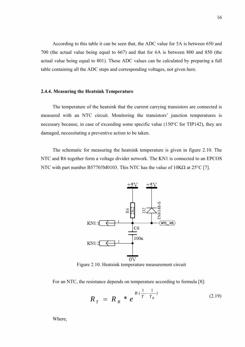
2.4.4. Measuring the Heatsink Temperature
The temperature of the heatsink that the current carrying transistors are connected is
measured with an NTC circuit. Monitoring the transistors’ junction temperatures is
necessary because, in case of exceeding some specific value (150°C for TIP142), they are
damaged, necessitating a preventive action to be taken.
The schematic for measuring the heatsink temperature is given in figure 2.10. The
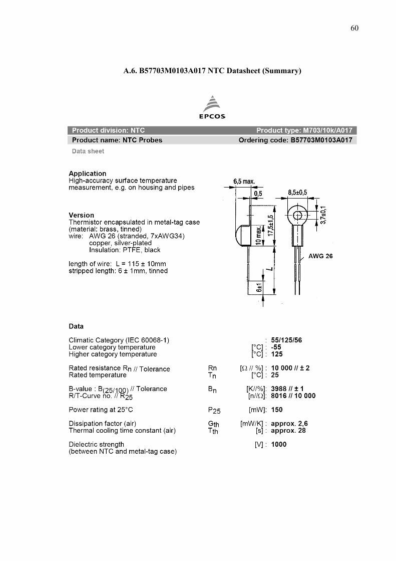
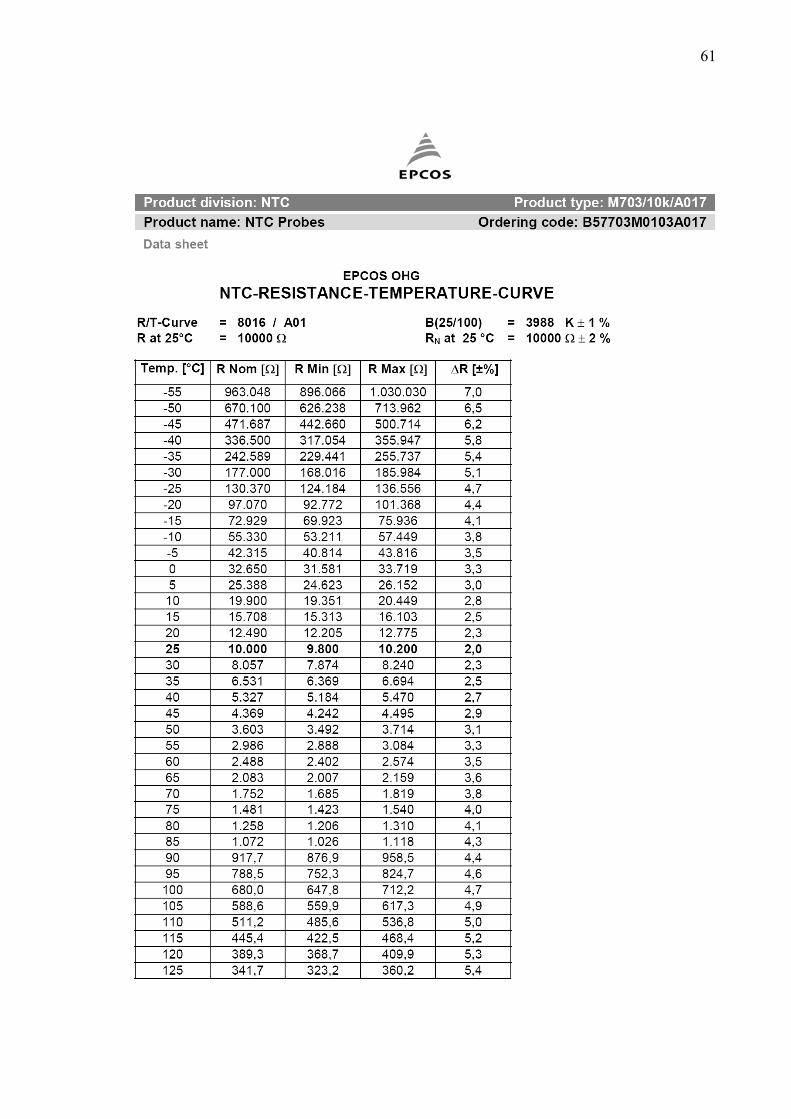
NTC and R6 together form a voltage divider network. The KN1 is connected to an EPCOS
NTC with part number B57703M0103. This NTC has the value of 10KΩ at 25°C [7].
Figure 2.10. Heatsink temperature measurement circuit
For an NTC, the resistance depends on temperature according to formula [8]:
)11(* RTT
B
RT eRR−
= (2.19)
Where,
17
RT: The resistance of NTC in Ω at temperature T in K°.
RR: The resistance of NTC in Ω at rated temperature T in K° ( 10KΩ for T=25°C).
T: Temperature in K°.
TR: Rated temperature in K°.
B: B value, material-specific constant of NTC thermistor.
RR
T
TRR
B
T 1)ln(11
+= (2.20)
For the NTC B57703M0103,
Ω= 10000RR (2.21)
KT R °=+= 29825273 (2.22)
3988=B (2.23)
So if RT is measured or calculated, T can also be calculated by using the above
formula and then converted to Celsius using (2.24).
273
2731)ln(1
1−
++
=
RR
TC
TRR
B
T (2.24)
The ADC input of the microcontroller is fed with the voltage which is set by the
value of the NTC and the series resistor R6.
18
6)( *
RRRVV
NTC
NTCCCNTCADC +
= (2.25)
The microcontroller receives this ADC value and calculates the voltage accordingly.
From this voltage value, the value of RNTC is calculated by the following formula:
)(6 *
NTCADCCC
CCNTC VV
VRR−
= (2.26)
VCC, which the microcontroller supply voltage, is equal to 5V and R6 is selected to be
2,2KΩ. After calculating this RNTC value, the temperature of the NTC and hence the
temperature of the heatsink are calculated according to the above formula.
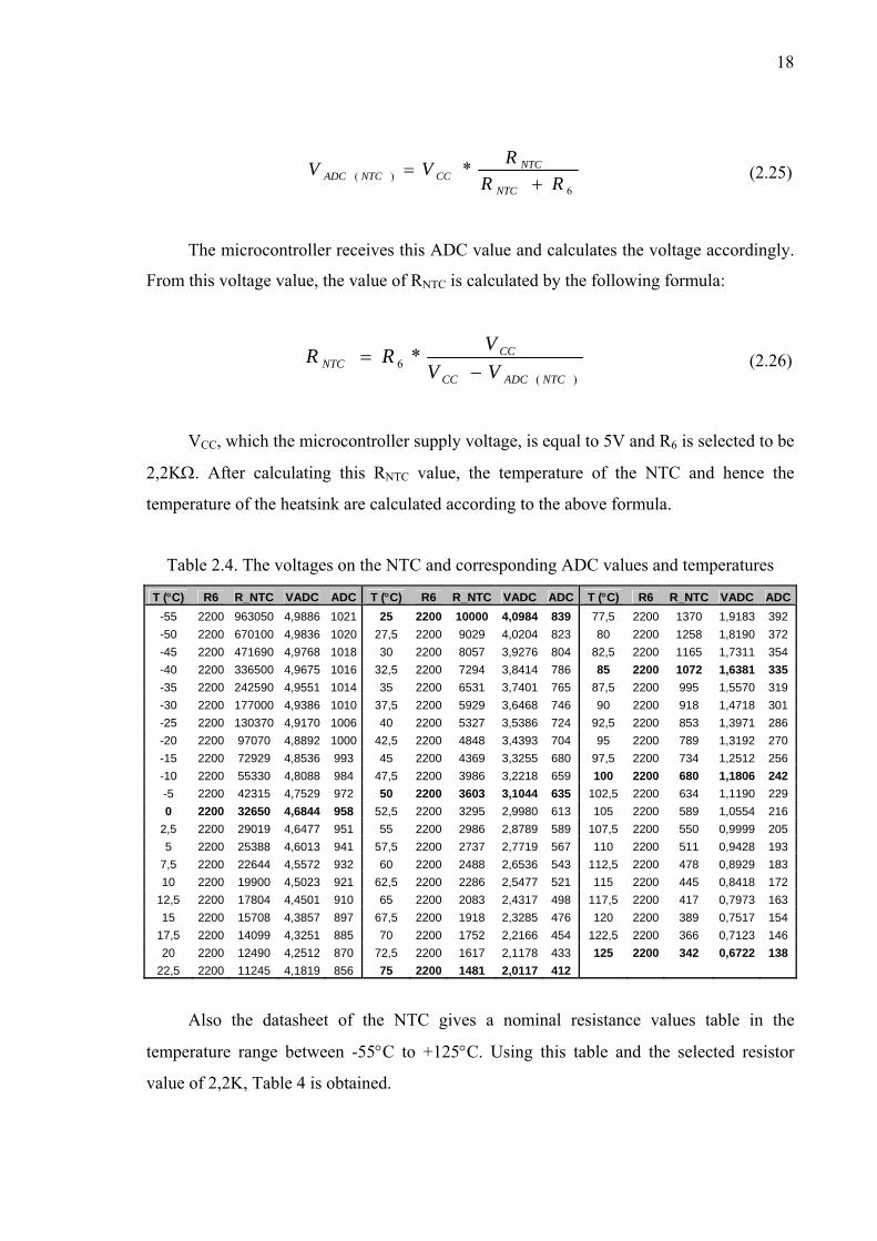
Table 2.4. The voltages on the NTC and corresponding ADC values and temperatures
T (°C) R6 R_NTC VADC ADC T (°C) R6 R_NTC VADC ADC T (°C) R6 R_NTC VADC ADC-55 2200 963050 4,9886 1021 25 2200 10000 4,0984 839 77,5 2200 1370 1,9183 392 -50 2200 670100 4,9836 1020 27,5 2200 9029 4,0204 823 80 2200 1258 1,8190 372 -45 2200 471690 4,9768 1018 30 2200 8057 3,9276 804 82,5 2200 1165 1,7311 354 -40 2200 336500 4,9675 1016 32,5 2200 7294 3,8414 786 85 2200 1072 1,6381 335 -35 2200 242590 4,9551 1014 35 2200 6531 3,7401 765 87,5 2200 995 1,5570 319 -30 2200 177000 4,9386 1010 37,5 2200 5929 3,6468 746 90 2200 918 1,4718 301 -25 2200 130370 4,9170 1006 40 2200 5327 3,5386 724 92,5 2200 853 1,3971 286 -20 2200 97070 4,8892 1000 42,5 2200 4848 3,4393 704 95 2200 789 1,3192 270 -15 2200 72929 4,8536 993 45 2200 4369 3,3255 680 97,5 2200 734 1,2512 256 -10 2200 55330 4,8088 984 47,5 2200 3986 3,2218 659 100 2200 680 1,1806 242 -5 2200 42315 4,7529 972 50 2200 3603 3,1044 635 102,5 2200 634 1,1190 229 0 2200 32650 4,6844 958 52,5 2200 3295 2,9980 613 105 2200 589 1,0554 216
2,5 2200 29019 4,6477 951 55 2200 2986 2,8789 589 107,5 2200 550 0,9999 205 5 2200 25388 4,6013 941 57,5 2200 2737 2,7719 567 110 2200 511 0,9428 193
7,5 2200 22644 4,5572 932 60 2200 2488 2,6536 543 112,5 2200 478 0,8929 183 10 2200 19900 4,5023 921 62,5 2200 2286 2,5477 521 115 2200 445 0,8418 172
12,5 2200 17804 4,4501 910 65 2200 2083 2,4317 498 117,5 2200 417 0,7973 163 15 2200 15708 4,3857 897 67,5 2200 1918 2,3285 476 120 2200 389 0,7517 154
17,5 2200 14099 4,3251 885 70 2200 1752 2,2166 454 122,5 2200 366 0,7123 146 20 2200 12490 4,2512 870 72,5 2200 1617 2,1178 433 125 2200 342 0,6722 138
22,5 2200 11245 4,1819 856 75 2200 1481 2,0117 412
Also the datasheet of the NTC gives a nominal resistance values table in the
temperature range between -55°C to +125°C. Using this table and the selected resistor
value of 2,2K, Table 4 is obtained.
19
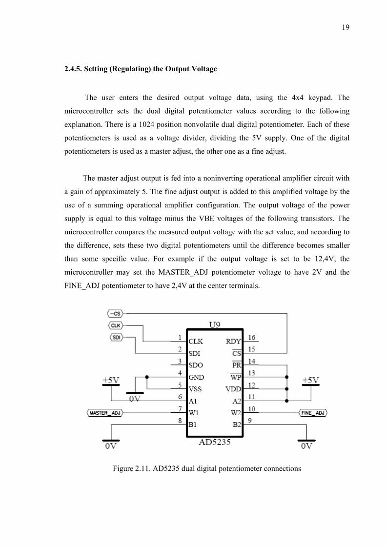
2.4.5. Setting (Regulating) the Output Voltage
The user enters the desired output voltage data, using the 4x4 keypad. The
microcontroller sets the dual digital potentiometer values according to the following
explanation. There is a 1024 position nonvolatile dual digital potentiometer. Each of these
potentiometers is used as a voltage divider, dividing the 5V supply. One of the digital
potentiometers is used as a master adjust, the other one as a fine adjust.
The master adjust output is fed into a noninverting operational amplifier circuit with
a gain of approximately 5. The fine adjust output is added to this amplified voltage by the
use of a summing operational amplifier configuration. The output voltage of the power
supply is equal to this voltage minus the VBE voltages of the following transistors. The
microcontroller compares the measured output voltage with the set value, and according to
the difference, sets these two digital potentiometers until the difference becomes smaller
than some specific value. For example if the output voltage is set to be 12,4V; the
microcontroller may set the MASTER_ADJ potentiometer voltage to have 2V and the
FINE_ADJ potentiometer to have 2,4V at the center terminals.
Figure 2.11. AD5235 dual digital potentiometer connections
20
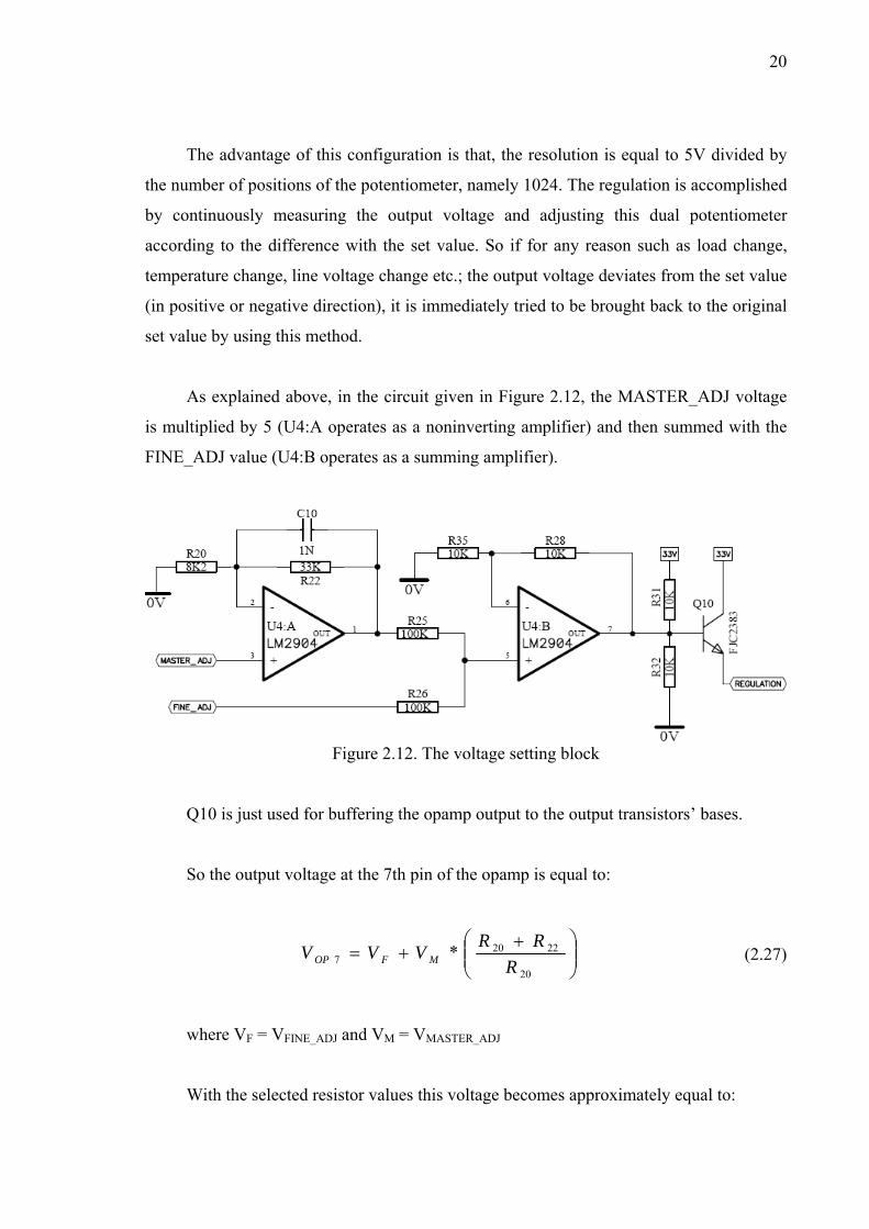
The advantage of this configuration is that, the resolution is equal to 5V divided by
the number of positions of the potentiometer, namely 1024. The regulation is accomplished
by continuously measuring the output voltage and adjusting this dual potentiometer
according to the difference with the set value. So if for any reason such as load change,
temperature change, line voltage change etc.; the output voltage deviates from the set value
(in positive or negative direction), it is immediately tried to be brought back to the original
set value by using this method.
As explained above, in the circuit given in Figure 2.12, the MASTER_ADJ voltage
is multiplied by 5 (U4:A operates as a noninverting amplifier) and then summed with the
FINE_ADJ value (U4:B operates as a summing amplifier).
Figure 2.12. The voltage setting block
Q10 is just used for buffering the opamp output to the output transistors’ bases.
So the output voltage at the 7th pin of the opamp is equal to:
⎟⎟⎠
⎞⎜⎜⎝
⎛ ++=
20
22207 *
RRRVVV MFOP (2.27)
where VF = VFINE_ADJ and VM = VMASTER_ADJ
With the selected resistor values this voltage becomes approximately equal to:
21
MFMFOP VVK
KKVVV *52,8
332,8*7 +≅⎟⎠
⎞⎜⎝
⎛ ++= (2.28)
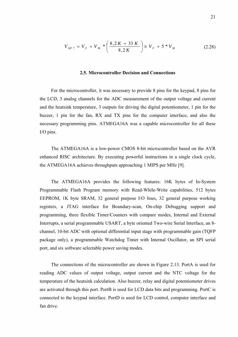
2.5. Microcontroller Decision and Connections
For the microcontroller, it was necessary to provide 8 pins for the keypad, 8 pins for
the LCD, 3 analog channels for the ADC measurement of the output voltage and current
and the heatsink temperature, 3 outputs for driving the digital potentiometer, 1 pin for the
buzzer, 1 pin for the fan, RX and TX pins for the computer interface, and also the
necessary programming pins. ATMEGA16A was a capable microcontroller for all these
I/O pins.
The ATMEGA16A is a low-power CMOS 8-bit microcontroller based on the AVR
enhanced RISC architecture. By executing powerful instructions in a single clock cycle,
the ATMEGA16A achieves throughputs approaching 1 MIPS per MHz [9].
The ATMEGA16A provides the following features: 16K bytes of In-System
Programmable Flash Program memory with Read-While-Write capabilities, 512 bytes
EEPROM, 1K byte SRAM, 32 general purpose I/O lines, 32 general purpose working
registers, a JTAG interface for Boundary-scan, On-chip Debugging support and
programming, three flexible Timer/Counters with compare modes, Internal and External
Interrupts, a serial programmable USART, a byte oriented Two-wire Serial Interface, an 8-
channel, 10-bit ADC with optional differential input stage with programmable gain (TQFP
package only), a programmable Watchdog Timer with Internal Oscillator, an SPI serial
port, and six software selectable power saving modes.
The connections of the microcontroller are shown in Figure 2.13. PortA is used for
reading ADC values of output voltage, output current and the NTC voltage for the
temperature of the heatsink calculation. Also buzzer, relay and digital potentiometer drives
are activated through this port. PortB is used for LCD data bits and programming. PortC is
connected to the keypad interface. PortD is used for LCD control, computer interface and
fan drive.
22
Figure 2.13. The microcontroller connections
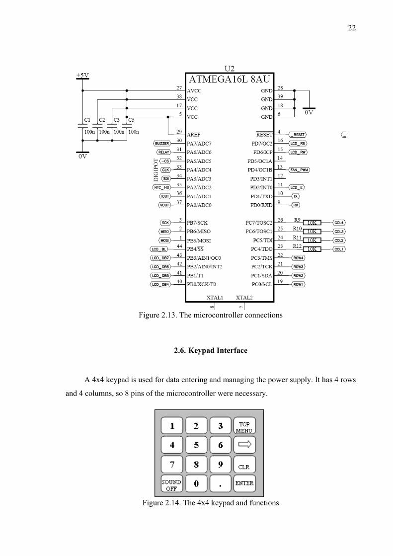
2.6. Keypad Interface
A 4x4 keypad is used for data entering and managing the power supply. It has 4 rows
and 4 columns, so 8 pins of the microcontroller were necessary.
Figure 2.14. The 4x4 keypad and functions
23
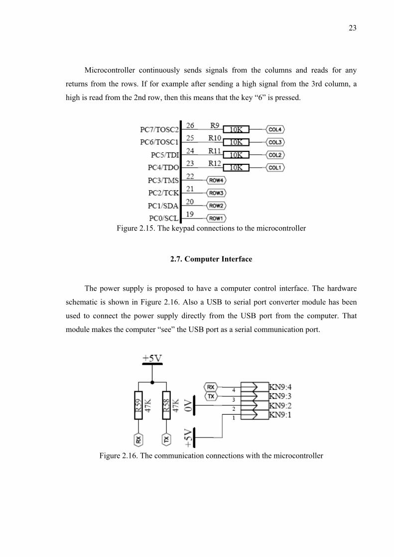
Microcontroller continuously sends signals from the columns and reads for any
returns from the rows. If for example after sending a high signal from the 3rd column, a
high is read from the 2nd row, then this means that the key “6” is pressed.
Figure 2.15. The keypad connections to the microcontroller
2.7. Computer Interface
The power supply is proposed to have a computer control interface. The hardware
schematic is shown in Figure 2.16. Also a USB to serial port converter module has been
used to connect the power supply directly from the USB port from the computer. That
module makes the computer “see” the USB port as a serial communication port.
Figure 2.16. The communication connections with the microcontroller
24
2.8. LCD Interface
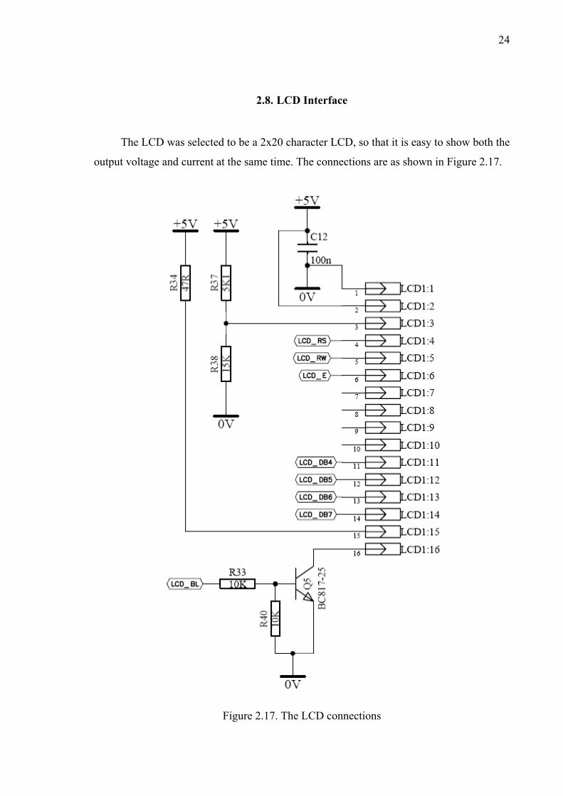
The LCD was selected to be a 2x20 character LCD, so that it is easy to show both the
output voltage and current at the same time. The connections are as shown in Figure 2.17.
Figure 2.17. The LCD connections
25
2.9. Microcontroller Programming
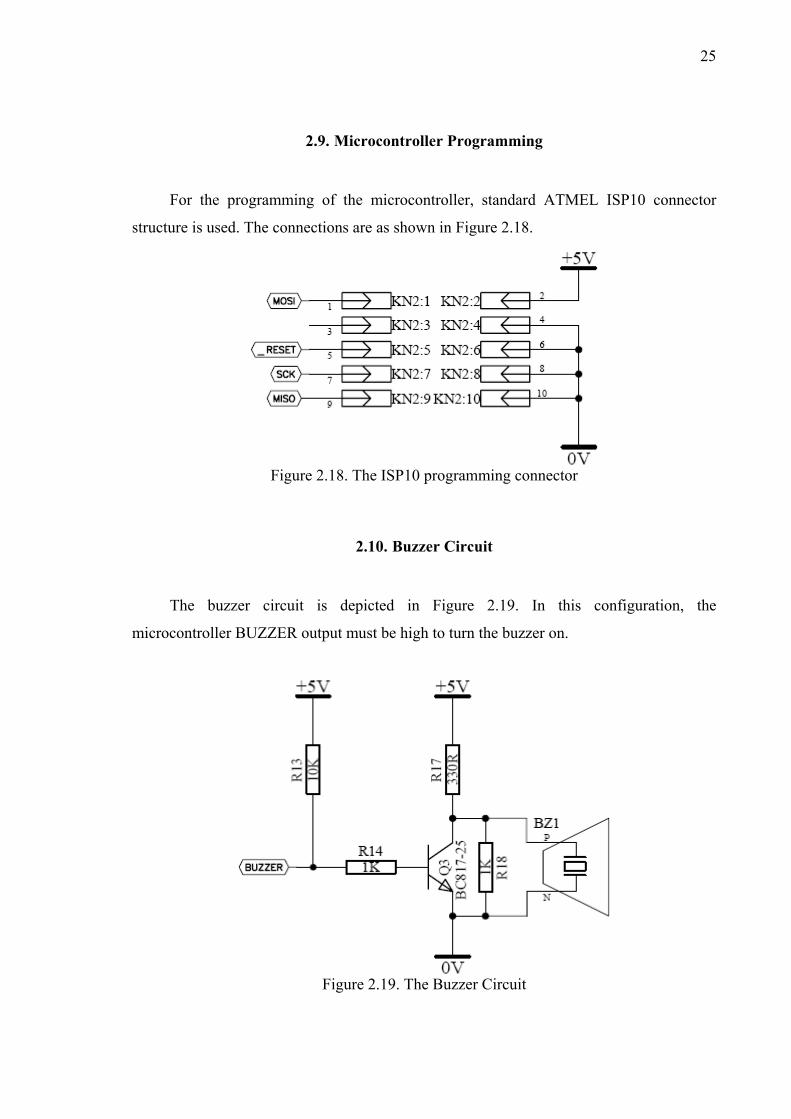
For the programming of the microcontroller, standard ATMEL ISP10 connector
structure is used. The connections are as shown in Figure 2.18.
Figure 2.18. The ISP10 programming connector
2.10. Buzzer Circuit
The buzzer circuit is depicted in Figure 2.19. In this configuration, the
microcontroller BUZZER output must be high to turn the buzzer on.
Figure 2.19. The Buzzer Circuit
26
2.11. Thermal (Heatsink) Considerations
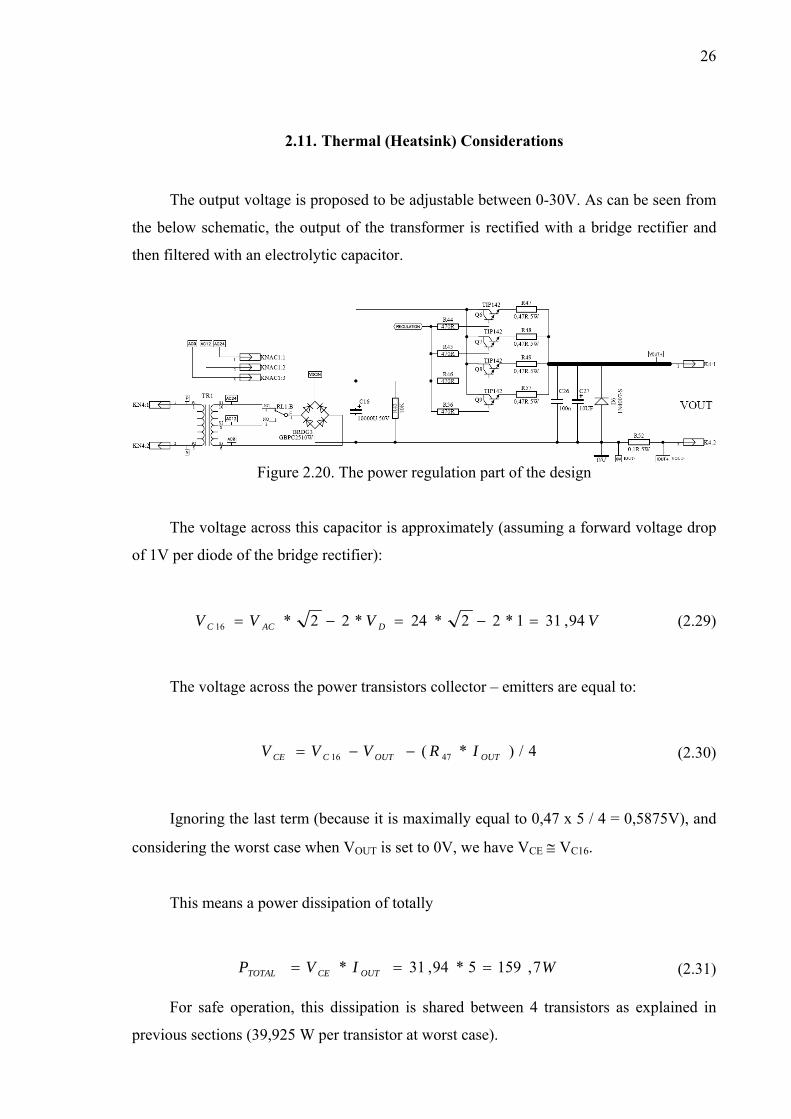
The output voltage is proposed to be adjustable between 0-30V. As can be seen from
the below schematic, the output of the transformer is rectified with a bridge rectifier and
then filtered with an electrolytic capacitor.
Figure 2.20. The power regulation part of the design
The voltage across this capacitor is approximately (assuming a forward voltage drop
of 1V per diode of the bridge rectifier):
VVVV DACC 94,311*22*24*22*16 =−=−= (2.29)
The voltage across the power transistors collector – emitters are equal to:
4/)*( 4716 OUTOUTCCE IRVVV −−= (2.30)
Ignoring the last term (because it is maximally equal to 0,47 x 5 / 4 = 0,5875V), and
considering the worst case when VOUT is set to 0V, we have VCE ≅ VC16.
This means a power dissipation of totally
WIVP OUTCETOTAL 7,1595*94,31* === (2.31)
For safe operation, this dissipation is shared between 4 transistors as explained in
previous sections (39,925 W per transistor at worst case).
27
Some additional action is taken to further reduce the power dissipation per transistor.
As can be seen from the schematic, the transformer has 3 taps; namely AC0, AC12 and
AC24. So when the output voltage is set below 13V, the AC12 terminal is used instead of
AC24. This is accomplished by switching a relay through the microcontroller control when
the user enters a voltage less then 13V. The power dissipations then become:
VV C 97,1422*1216 =−= (2.32)
WIVP OUTCETOTAL 85,745*97,14* === (2.33)
In this case, the dissipation per transistor is reduced to 74,85 / 4 = 18,71W.
There is also a fan attached to the heatsink of these power transistors, which
normally is off. This fan is turned on when the temperature measurement made by the
microcontroller by using the NTC exceeds some specified value (50°C).
As explained before, for TIP142 transistors, Tjmax = 150°C. Power dissipation per
transistor was previously calculated to be 18,71W at worst case.
For this power supply, it is assumed that the maximum working ambient temperature
is Tamb = 50°C.
Combining the above, the necessary total thermal resistance from one transistor’s
junction to ambient is calculated as:
)/(34,571,18
50150max)(1 WC
PdTambTjR ajth °=
−=
−=− (2.34)
Using the TIP142 datasheet, thermal resistance for the TO-3P package transistor is
given as Rth1(j-c) = 1 °C/W. Since Rth1(j-a) is equal to:
28
)(1)(1)(1)(1 ahsthhscthcjthajth RRRR −−−− ++= (2.35)
Assuming Rth1(c-hs) = 0,5 °C/W;
)/(84,315,034,5)(1 WCR ahsth °=−−=− (2.36)
Because the same heatsink is used for 4 transistors, the necessary thermal resistance
for the overall heatsink is calculated to be
)/(96,04/84,3)(4 WCR ahsth °==− (2.37)
By using the demo software, “Hsink” from Frigus Primore, the thermal simulations
are realized [10]. The four transistors’ TO-3P packages and their placements on the
heatsink were defined to this program as in Figure 2.21 (the same as in the real
application). Each transistor is defined as a heat source. Also the power dissipation on each
transistor is entered to be 18,7W (which is the maximum calculated) to the dissipation
cells.
Figure 2.21. The heatsink simulation showing the power dissipations
29
The dimensions and the fin counts were also entered in that program. (The demo
version allows 50mm for the depth, although the actual heatsink used was 70mm.
Figure 2.22. The heatsink simulation showing the heatsink dimensions
The simulations revealed a thermal resistance of 0,81°C/W for the heatsink defined
assuming 1m/s air velocity.
Figure 2.23. The 3D model for the heatsink and the transistors as heat sources
The distribution on the heatsink resulting from the simulation is depicted in Figure
2.24. It is seen that the transistors in the middle become the most heated. This is as
expected since it is easier for the outer transistors to radiate heat with the help of the
heatsink since they are able to use more fins. Using this result of the simulation, the fan is
directed to the part of the heatsink where these transistors are mounted.

30
Figure 2.24. The result of the heatsink simulation showing the heat distribution
2.12. Output Overcurrent Protection
The output current is continuously monitored and displayed. If is exceeds 6A, the
microcontroller immediately lowers the output voltage until the output current is below 6A
and turns the buzzer signal on.
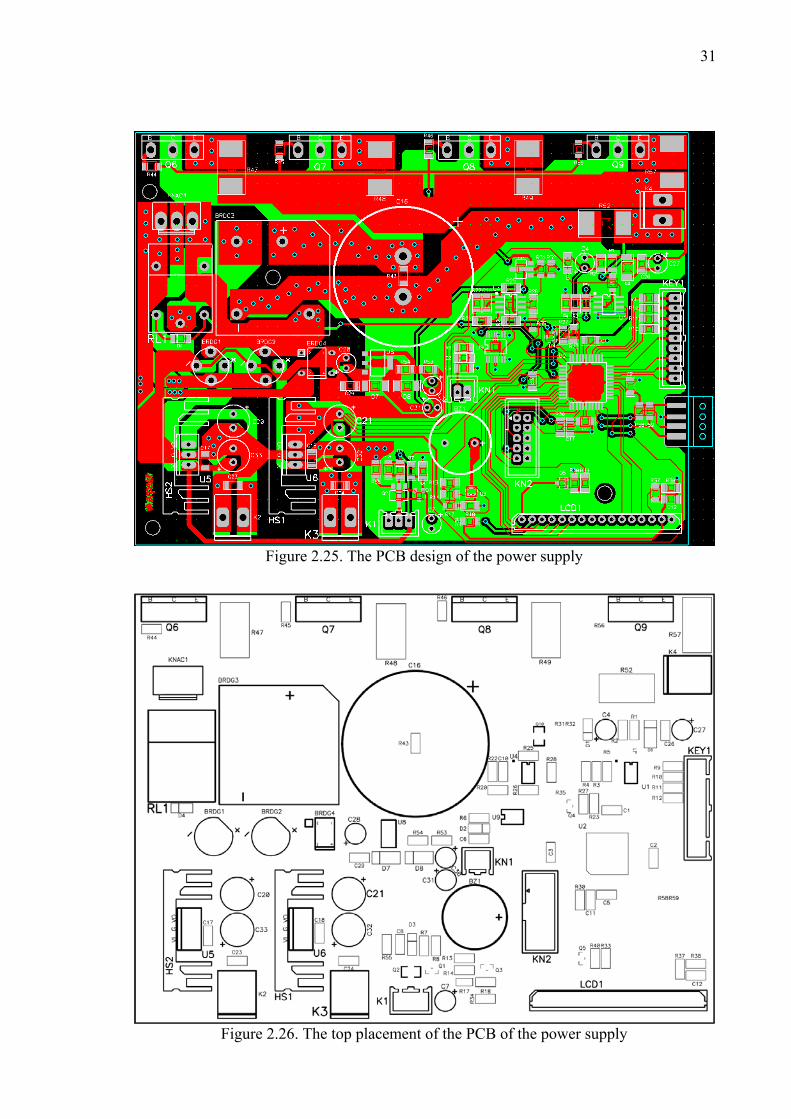
2.13. The PCB Design
The PCB design directly affects the proper operation of the power supply, therefore
it is very important
Utmost efficiency is aimed in the placement within the power supply box. The
approach was to place the power part and the controller parts as separate blocks and then to
combine them.
It was important for the routing of current carrying routes to be thick enough. Also
for the analog measurement paths, care was taken not to create long loops so that the
measurements were minimally affected.
31
Figure 2.25. The PCB design of the power supply
Figure 2.26. The top placement of the PCB of the power supply
32
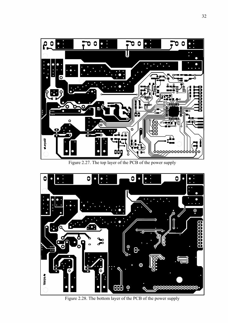
Figure 2.27. The top layer of the PCB of the power supply
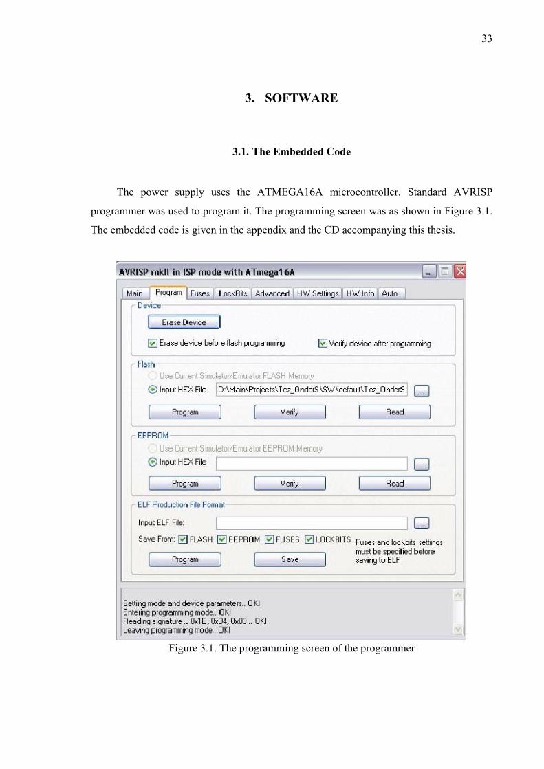
Figure 2.28. The bottom layer of the PCB of the power supply
33
3. SOFTWARE
3.1. The Embedded Code
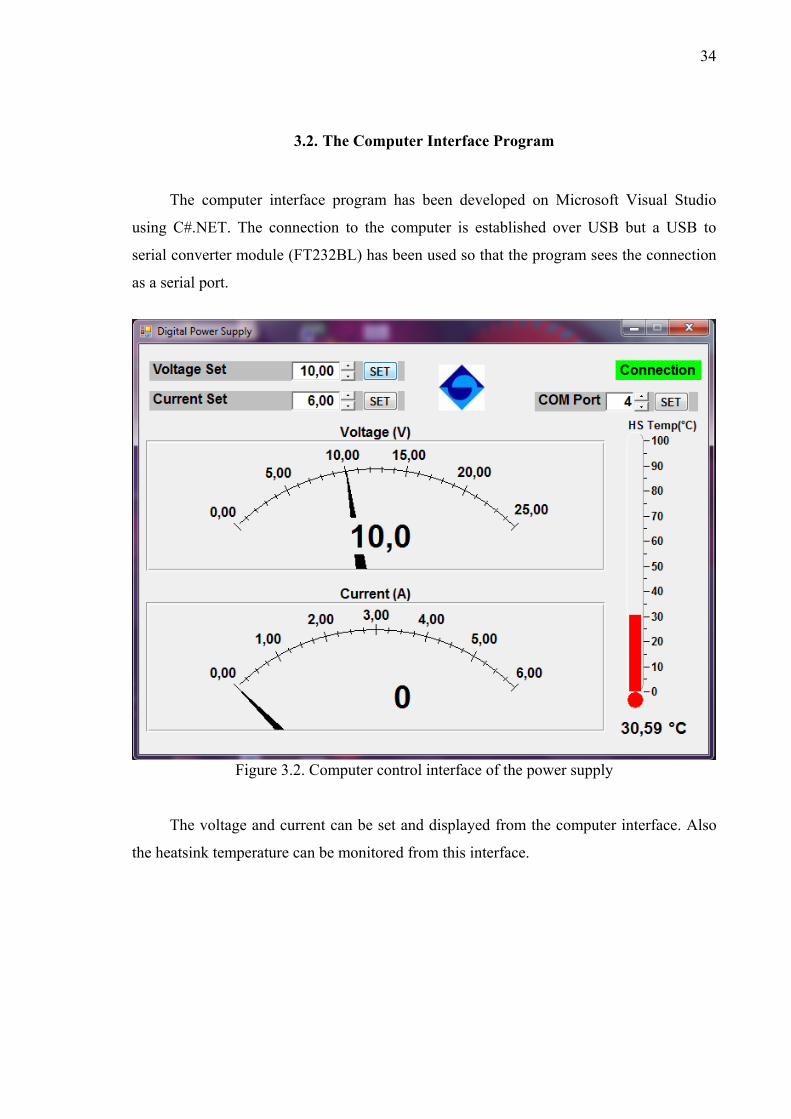
The power supply uses the ATMEGA16A microcontroller. Standard AVRISP
programmer was used to program it. The programming screen was as shown in Figure 3.1.
The embedded code is given in the appendix and the CD accompanying this thesis.
Figure 3.1. The programming screen of the programmer
34
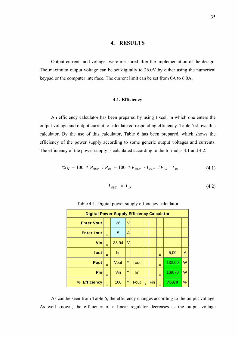
3.2. The Computer Interface Program
The computer interface program has been developed on Microsoft Visual Studio
using C#.NET. The connection to the computer is established over USB but a USB to
serial converter module (FT232BL) has been used so that the program sees the connection
as a serial port.
Figure 3.2. Computer control interface of the power supply
The voltage and current can be set and displayed from the computer interface. Also
the heatsink temperature can be monitored from this interface.
35
4. RESULTS
Output currents and voltages were measured after the implementation of the design.
The maximum output voltage can be set digitally to 26.0V by either using the numerical
keypad or the computer interface. The current limit can be set from 0A to 6.0A.
4.1. Efficiency
An efficiency calculator has been prepared by using Excel, in which one enters the
output voltage and output current to calculate corresponding efficiency. Table 5 shows this
calculator. By the use of this calculator, Table 6 has been prepared, which shows the
efficiency of the power supply according to some generic output voltages and currents.
The efficiency of the power supply is calculated according to the formulas 4.1 and 4.2.
ININOUTOUTINOUT IVIVPP ⋅⋅== /*100/*100%η (4.1)
INOUT II = (4.2)
Table 4.1. Digital power supply efficiency calculator
Digital Power Supply Efficiency Calculator
Enter Vout = 26 V
Enter Iout = 5 A
Vin = 33,94 V
Iout = Iin
= 5,00 A
Pout = Vout * Iout
= 130,00 W
Pin = Vin * Iin
= 169,70 W
% Efficiency = 100 * Pout
/ Pin = 76,60 %
As can be seen from Table 6, the efficiency changes according to the output voltage.
As well known, the efficiency of a linear regulator decreases as the output voltage
36
decreases due to the increase of the voltage drop on the series pass transistors. So with the
designed power supply, the maximum efficiency that can be achieved is equal to %76,60,
because the output cannot reach up to 30V as explained.
Table 4.2. Efficiency of the power supply for various output voltages and currents
Iout (A)
Vout (V) 1,00 2,00 3,00 4,00 5,00
5,00 14,73 14,73 14,73 14,73 14,73
10,00 29,46 29,46 29,46 29,46 29,46
15,00 44,19 44,19 44,19 44,19 44,19
20,00 58,93 58,93 58,93 58,93 58,93
25,00 73,66 73,66 73,66 73,66 73,66
26,00 76,60 76,60 76,60 76,60 76,60
30,00 88,39 88,39 88,39 88,39 88,39
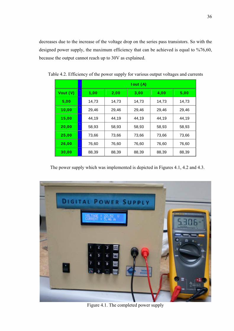
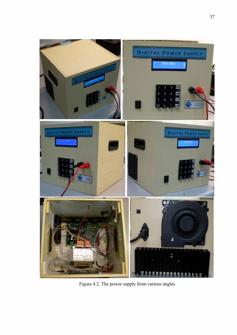
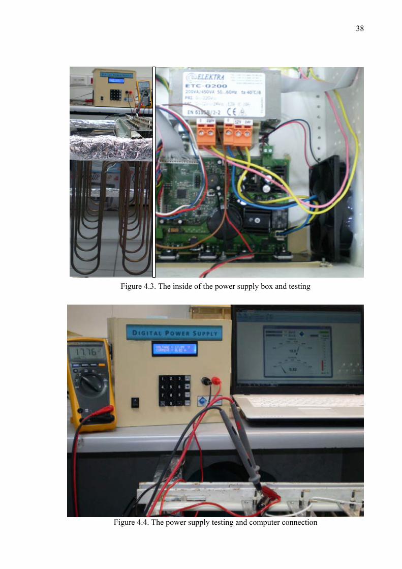
The power supply which was implemented is depicted in Figures 4.1, 4.2 and 4.3.
Figure 4.1. The completed power supply
37
Figure 4.2. The power supply from various angles
38
Figure 4.3. The inside of the power supply box and testing
Figure 4.4. The power supply testing and computer connection
39
5. CONCLUSION & FUTURE WORK
The digital power supply designed here accomplishes the tasks proposed to some
degree, but it may further be improved. Some of these improvements were mentioned in
the previous sections but discuses further in this section. Most of the improvements
explained in this section can be made easily to some degree, without making significant
changes or updates.
Current and voltage measurement topologies in this design are thought to be
sufficient for the tasks needed here. On the other hand, the resistor values, so the gains of
the measurement circuits may be optimized by considering the use of full scale of the ADC
resolution. To this end, first the operational amplifiers must be changed to rail-to-rail types.
Then for the output current, the measurements may be made with 5A / 1024 = 4,88mA
resolution, and for the output voltage with 30V / 1024 = 29,3mV resolution.
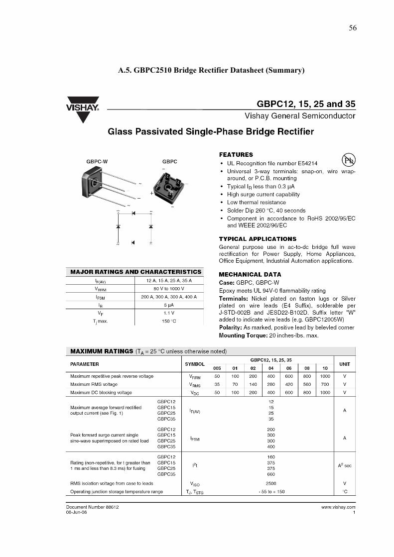
The main bridge rectifier of the design has power dissipation per leg (maximally)
WVAVfIfPLEG 51.5* === (5.1)
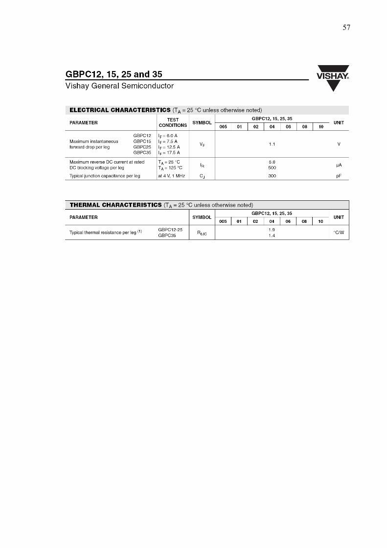
The datasheet gives RθJC = 1,9°C/W thermal resistance per leg [11], so this yields
CPLEGHeat LEG °=== 5,99,1*5R* JCθ (5.2)
For 4 legs, 9,5 x 4 = 38°C heat increase in total. Although a heatsink is attached to
this bridge rectifier, the reliability may further be improved by connecting this bridge
rectifier to the main heatsink.
Although it is proposed for the digital power supply to have maximally 5A output
current, with the current topology it may be easily upgraded to higher values, even without
making any changes to the number of power transistors. For the present prototype, it was
tested up to 6A without any problems.
40
The power supply has a controlled fan drive, meaning that when the heat of the
heatsink exceeds 50°C, the microcontroller drives the fan until the heatsink temperature
falls below 40°C. This fan drive may be improved by using a PWM drive so that the power
dissipated to drive the fan can be decreased. Also the mechanical design may be changed
so that the fan blows through both the heatsink and the PCB.
The output voltage of the power supply can be set up to 26V for this prototype. The
related calculations are given below:
The AC input voltage of the power supply is 24VAC with a peak voltage of
VVV ACinDC 94,33*2_ == (5.3)
After the diode bridge, because of two forward voltage drops against the bridge
rectifier, it becomes
VVVV FinDCDC 94,31*2_ =−= (5.4)
For the LM317 unit, according to the datasheet [12],
)53*(54531317 RI
RRVV adjrLM +⎟
⎠⎞
⎜⎝⎛ += (5.5)
VuAVVLM 65,32)3000*50(1203000125,1317 =+⎟
⎠⎞
⎜⎝⎛ += (5.6)
But because the input to output differential voltage of the LM317 is minimally 3V,
VVVV DROPDCMAXOUTLM 94,28394,31)(317 =−=−= (5.7)
41
So the voltage labeled as 33V in the power part schematic (output of the LM317) is
in fact maximally equal to 28,94V. This is the supply voltage of the opamp and transistor
of the control part of the circuit where the output of the digital potentiometer drives the
regulator transistors.
Figure 5.1. Digital potentiometer part
So the output of the U4:B can maximally be equal to
VVV CCBU 44,275,194,285,14 =−=−= (5.8)
Assuming the VBE of FJC2383 to be 0,7V, the maximum value of the control voltage
at the bases of the regulator transistors becomes equal to
VVVV QBEBUREGULATION 74,267,044,27)10(4 =−=−= (5.9)
According to these calculations and assumptions, the maximum DC output voltage is
)6(47__ )4/(* QBEOUTMAXREGULATIONMAXOUTDC VIRVV −−= (5.10)
VV MAXOUTDC 035,233)4/6(*47,074,26__ =−−= (5.11)
By using a transformer with 26VAC output instead of 24VAC output, a maximum of
26,17V can be achieved.
42
APPENDIX A: DATASHEETS
A.1. TIP142 Datasheet
43
44
45
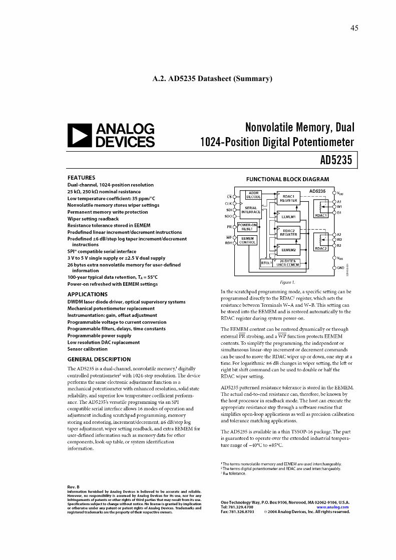
A.2. AD5235 Datasheet (Summary)
46
47

48
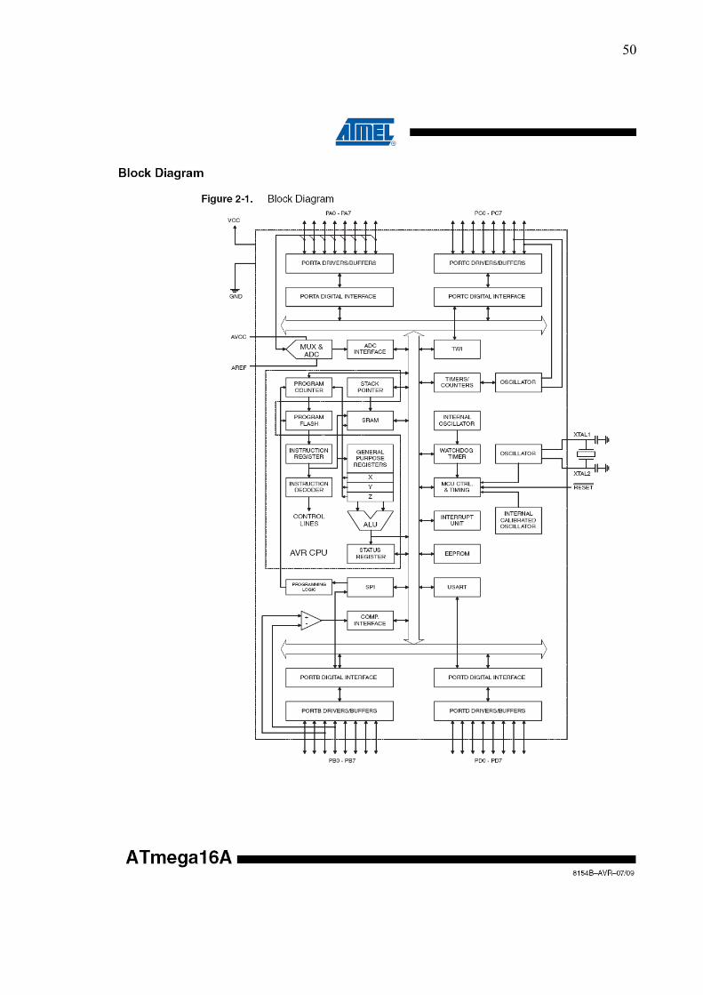
A.3. ATMEGA16 Datasheet (Summary)
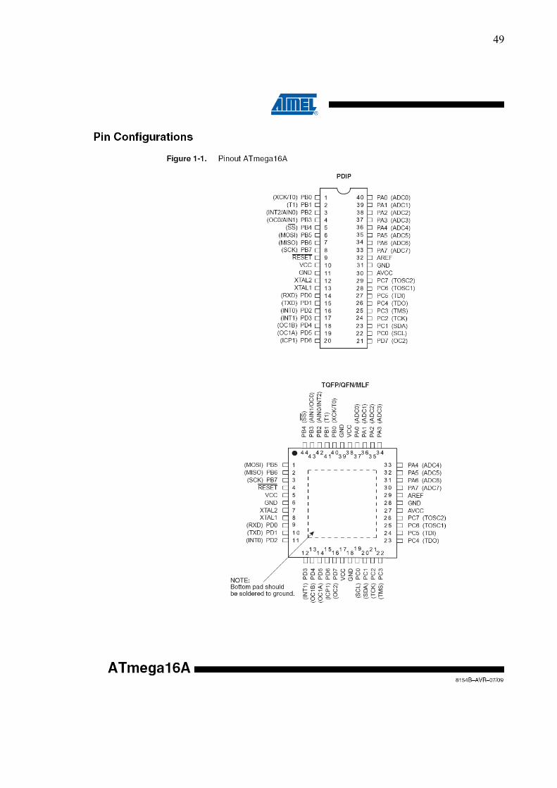
49
50

51
52
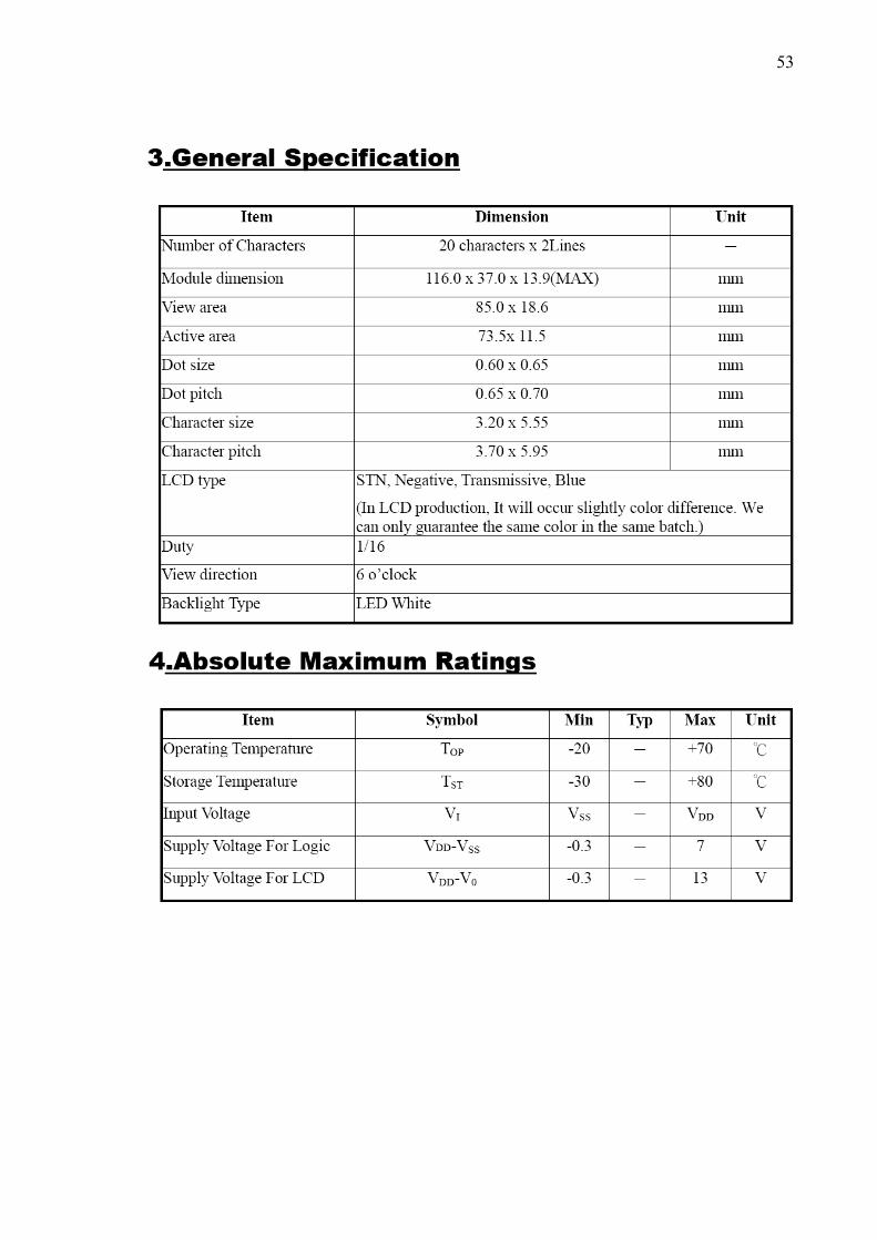
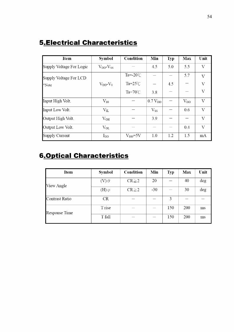
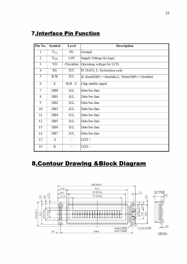
A.4. WH2002A-TMI-ET LCD Datasheet (Summary)
53
54
55
56
A.5. GBPC2510 Bridge Rectifier Datasheet (Summary)
57
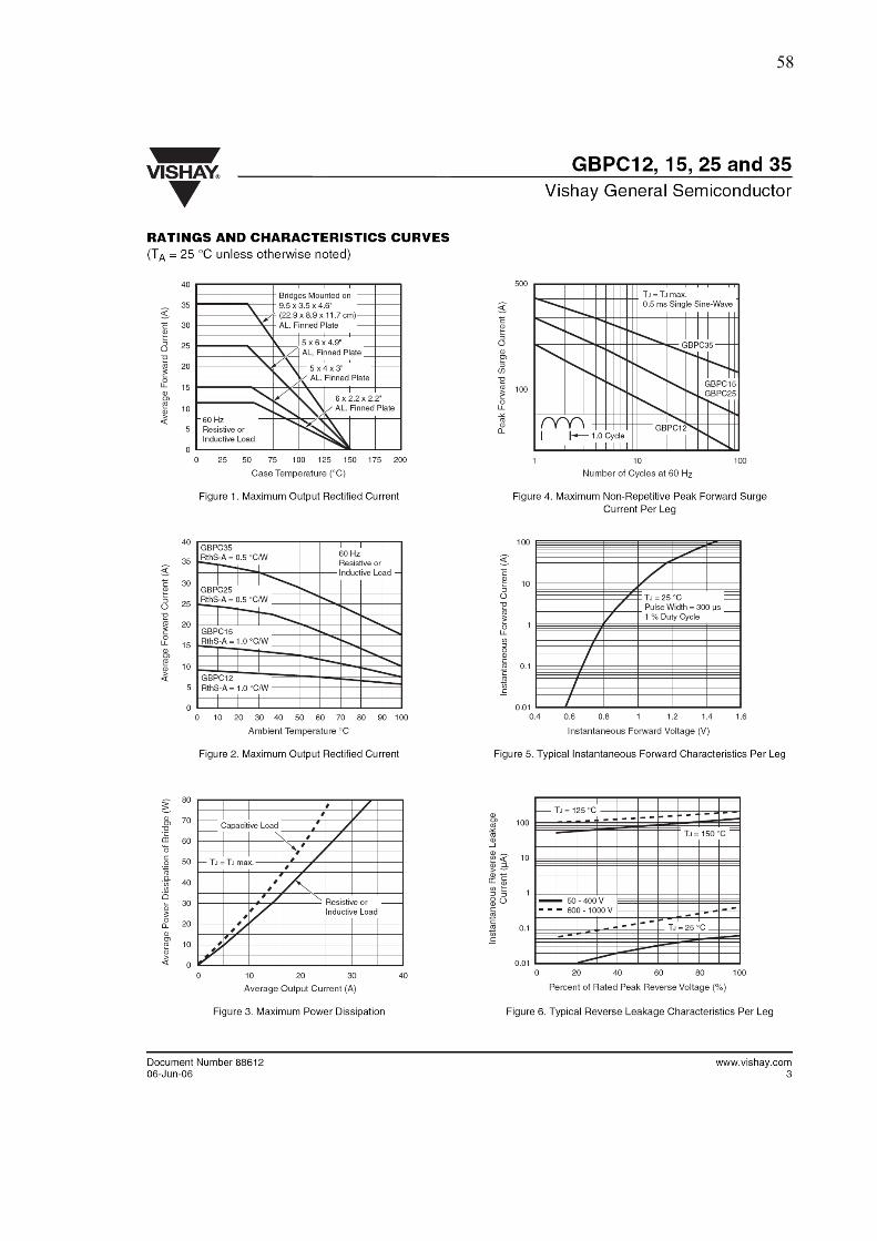
58
59
60
A.6. B57703M0103A017 NTC Datasheet (Summary)
61
62
APPENDIX B: EMBEDDED CODE
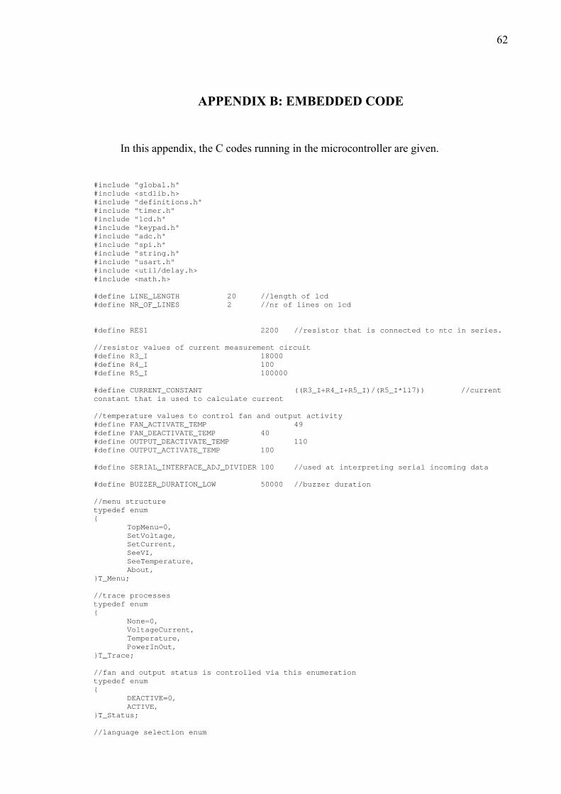
In this appendix, the C codes running in the microcontroller are given.
#include "global.h" #include <stdlib.h> #include "definitions.h" #include "timer.h" #include "lcd.h" #include "keypad.h" #include "adc.h" #include "spi.h" #include "string.h" #include "usart.h" #include <util/delay.h> #include <math.h> #define LINE_LENGTH 20 //length of lcd #define NR_OF_LINES 2 //nr of lines on lcd #define RES1 2200 //resistor that is connected to ntc in series. //resistor values of current measurement circuit #define R3_I 18000 #define R4_I 100 #define R5_I 100000 #define CURRENT_CONSTANT ((R3_I+R4_I+R5_I)/(R5_I*117)) //current constant that is used to calculate current //temperature values to control fan and output activity #define FAN_ACTIVATE_TEMP 49 #define FAN_DEACTIVATE_TEMP 40 #define OUTPUT_DEACTIVATE_TEMP 110 #define OUTPUT_ACTIVATE_TEMP 100 #define SERIAL_INTERFACE_ADJ_DIVIDER 100 //used at interpreting serial incoming data #define BUZZER_DURATION_LOW 50000 //buzzer duration //menu structure typedef enum { TopMenu=0, SetVoltage, SetCurrent, SeeVI, SeeTemperature, About, }T_Menu; //trace processes typedef enum { None=0, VoltageCurrent, Temperature, PowerInOut, }T_Trace; //fan and output status is controlled via this enumeration typedef enum { DEACTIVE=0, ACTIVE, }T_Status; //language selection enum
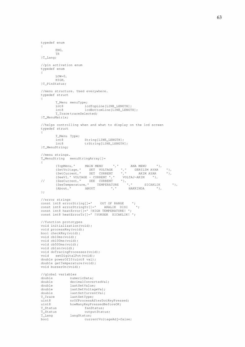
63
typedef enum { ENG, TR }T_Lang; //pin activation enum typedef enum { LOW=0, HIGH, }T_PinStatus; //menu structure. Used everywhere. typedef struct { T_Menu menuType; int8 lcdTopLine[LINE_LENGTH]; int8 lcdBottomLine[LINE_LENGTH]; T_Trace traceSelected; }T_MenuMatrix; //helps controlling when and what to display on the lcd screen typedef struct { T_Menu Type; int8 String[LINE_LENGTH]; int8 trString[LINE_LENGTH]; }T_MenuString; //menu strings. T_MenuString menuStringArray[]= { {TopMenu," MAIN MENU "," ANA MENU "}, {SetVoltage," SET VOLTAGE "," GERILIM AYAR "}, {SetCurrent," SET CURRENT "," AKIM AYAR "}, {SeeVI," VOLTAGE - CURRENT "," VOLTAJ-AKIM "}, // {SeeCurrent," SEE CURRENT "}, {SeeTemperature," TEMPERATURE "," SICAKLIK "}, {About," ABOUT "," HAKKINDA "}, }; //error strings const int8 errorString[]=" OUT OF RANGE "; const int8 errorStringTr[]=" ARALIK DISI "; const int8 heatError[]=" !HIGH TEMPERATURE! "; const int8 heatErrorTr[]=" !YUKSEK SICAKLIK! "; //function prototypes void initialization(void); void processKey(void); bool checkKey(void); void cb10ms(void); void cb100ms(void); void cb500ms(void); void cb1sn(void); void doTracingProcesses(void); void setDigitalPot(void); double powerOf10(uint8 val); double getTemperature(void); void buzzerOn(void); //global variables double numericData; double decimalConvertedVal; double lastSetValue; double lastSetVoltageVal; double lastSetCurrentVal; T_Trace lastSetType; uint8 nrOfProcessAfterDotKeyPressed; uint8 howManyKeyPressedBeforeOK; T_Status fanStatus; T_Status outputStatus; T_Lang langStatus; bool currentVoltageAdj=false;
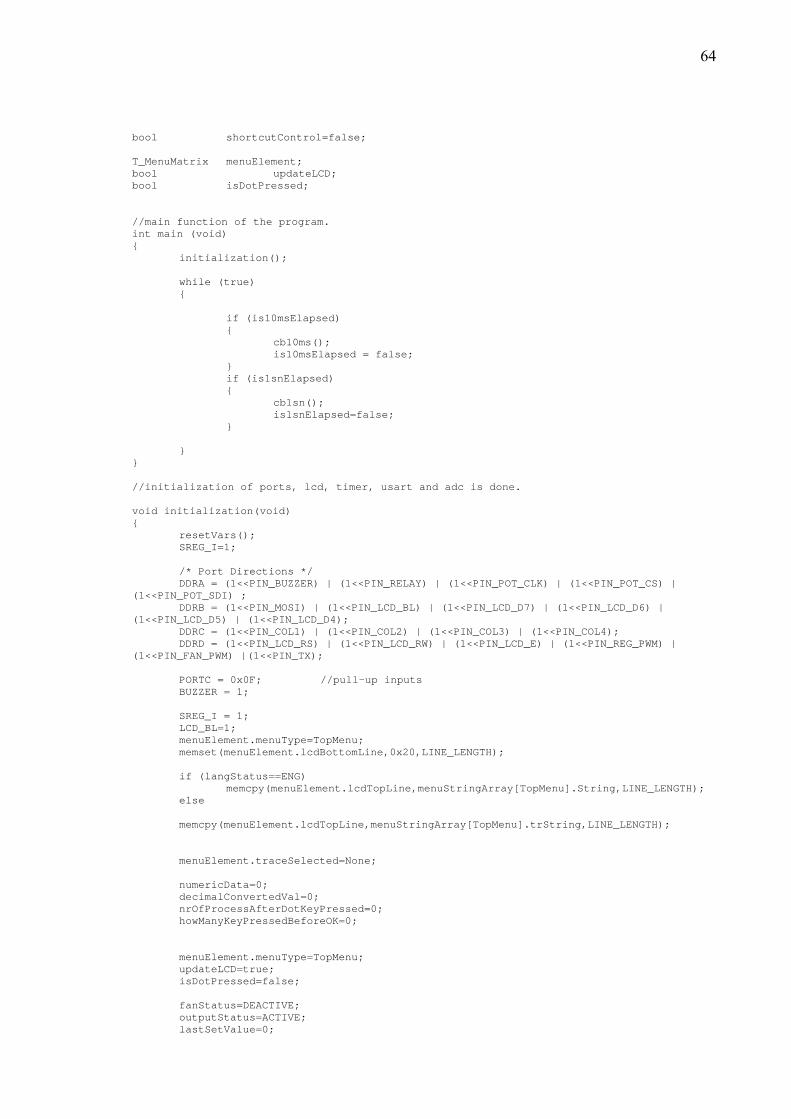
64
bool shortcutControl=false; T_MenuMatrix menuElement; bool updateLCD; bool isDotPressed; //main function of the program. int main (void) { initialization(); while (true) { if (is10msElapsed) { cb10ms(); is10msElapsed = false; } if (is1snElapsed) { cb1sn(); is1snElapsed=false; } } } //initialization of ports, lcd, timer, usart and adc is done. void initialization(void) { resetVars(); SREG_I=1; /* Port Directions */ DDRA = (1<<PIN_BUZZER) | (1<<PIN_RELAY) | (1<<PIN_POT_CLK) | (1<<PIN_POT_CS) | (1<<PIN_POT_SDI) ; DDRB = (1<<PIN_MOSI) | (1<<PIN_LCD_BL) | (1<<PIN_LCD_D7) | (1<<PIN_LCD_D6) | (1<<PIN_LCD_D5) | (1<<PIN_LCD_D4); DDRC = (1<<PIN_COL1) | (1<<PIN_COL2) | (1<<PIN_COL3) | (1<<PIN_COL4); DDRD = (1<<PIN_LCD_RS) | (1<<PIN_LCD_RW) | (1<<PIN_LCD_E) | (1<<PIN_REG_PWM) | (1<<PIN_FAN_PWM) |(1<<PIN_TX); PORTC = 0x0F; //pull-up inputs BUZZER = 1; SREG_I = 1; LCD_BL=1; menuElement.menuType=TopMenu; memset(menuElement.lcdBottomLine,0x20,LINE_LENGTH); if (langStatus==ENG) memcpy(menuElement.lcdTopLine,menuStringArray[TopMenu].String,LINE_LENGTH); else memcpy(menuElement.lcdTopLine,menuStringArray[TopMenu].trString,LINE_LENGTH); menuElement.traceSelected=None; numericData=0; decimalConvertedVal=0; nrOfProcessAfterDotKeyPressed=0; howManyKeyPressedBeforeOK=0; menuElement.menuType=TopMenu; updateLCD=true; isDotPressed=false; fanStatus=DEACTIVE; outputStatus=ACTIVE; lastSetValue=0;
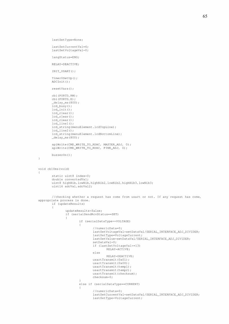
65
lastSetType=None; lastSetCurrentVal=6; lastSetVoltageVal=0; langStatus=ENG; RELAY=DEACTIVE; INIT_USART(); Timer0SetUp(); ADCInit(); resetVars(); cbi(PORTD,RW); cbi(PORTD,E); _delay_ms(800); lcd_busy(); lcd_init(); lcd_clear(); lcd_clear(); lcd_clear(); lcd_line1(); lcd_string(menuElement.lcdTopLine); lcd_line2(); lcd_string(menuElement.lcdBottomLine); _delay_ms(800); spiWrite(CMD_WRITE_TO_RDAC, MASTER_ADJ, 0); spiWrite(CMD_WRITE_TO_RDAC, FINE_ADJ, 0); buzzerOn(); } void cb10ms(void) { static uint8 index=0; double convertedVal; uint8 highNib,lowNib,highNib2,lowNib2,highNib3,lowNib3; uint16 adcVal,adcVal2; //checking whether a request has come from usart or not. If any request has come, appropriate process is done. if (updateResults) { updateResults=false; if (serialSendRcvStatus==SET) { if (serialDataType==VOLTAGE) { //numericData=0; lastSetVoltageVal=setDataVal/SERIAL_INTERFACE_ADJ_DIVIDER; lastSetType=VoltageCurrent; lastSetValue=setDataVal/SERIAL_INTERFACE_ADJ_DIVIDER; setDataVal=0; if (lastSetVoltageVal>=13) RELAY=ACTIVE; else RELAY=DEACTIVE; usartTransmit(0x01); usartTransmit(0x00); usartTransmit(temp1); usartTransmit(temp2); usartTransmit(checksum); checksum=0; } else if (serialDataType==CURRENT) { //numericData=0; lastSetCurrentVal=setDataVal/SERIAL_INTERFACE_ADJ_DIVIDER; lastSetType=VoltageCurrent;
66
lastSetValue=setDataVal/SERIAL_INTERFACE_ADJ_DIVIDER; setDataVal=0; usartTransmit(0x01); usartTransmit(0x01); usartTransmit(temp1); usartTransmit(temp2); usartTransmit(checksum); checksum=0; } } else if (serialSendRcvStatus==GET) { uint32 dene; adcVal = getValueOfADCChannel(ADC_V); adcVal2=getValueOfADCChannel(ADC_I); convertedVal=((((((double)adcVal*(double)1.31)/(26.5))*0.7948)+0.0515)*0.9419-0.0232)-(0.1*adcVal2*CURRENT_CONSTANT); convertedVal*=100; highNib=convertedVal/256; lowNib=(uint8)(((uint16)(convertedVal))&0x00FF); convertedVal=(double)(adcVal2)/117; convertedVal=convertedVal*((R3_I+R4_I+R5_I)/(R5_I)); convertedVal*=100; highNib2=convertedVal/256; lowNib2=(uint8)(((uint16)(convertedVal))&0x00FF); convertedVal=getTemperature(); convertedVal*=100; highNib3=convertedVal/256; lowNib3=(uint8)(((uint16)(convertedVal))&0x00FF); usartTransmit(2); usartTransmit(highNib); usartTransmit(lowNib); usartTransmit(highNib2); usartTransmit(lowNib2); usartTransmit(highNib3); usartTransmit(lowNib3); dene=((highNib3+lowNib3+highNib2+lowNib2+highNib+lowNib+2)%256); usartTransmit(255-(uint8)dene); } } //shortcut control by directly reading adc channel if (getValueOfADCChannel(ADC_I)>744) { spiWrite(CMD_WRITE_TO_RDAC, MASTER_ADJ, 0); spiWrite(CMD_WRITE_TO_RDAC, FINE_ADJ, 0); numericData=0; shortcutControl=true; } else { shortcutControl=false; } if (++index>=2) //every 20 ms, check keypad. { if (outputStatus == ACTIVE) { if (keypadPoll()) { buzzerOn(); processKey(); } }
67
else { memset(menuElement.lcdBottomLine,0x20,LINE_LENGTH); memset(menuElement.lcdTopLine,0x20,LINE_LENGTH); if (langStatus==ENG) strcpy(menuElement.lcdTopLine,heatError); else strcpy(menuElement.lcdTopLine,heatErrorTr); } index=0; } //update lcd if it is necessary if (updateLCD) { lcd_clear(); lcd_line1(); lcd_string(menuElement.lcdTopLine); lcd_line2(); lcd_string(menuElement.lcdBottomLine); updateLCD = false; } } //every 1 second, trace voltage and current values and adjust digital potentiometer according to user entered values. //Controlling fan activation and output status void cb1sn(void) { uint16 temp; doTracingProcesses(); if (checkTopMenuKey()) { initialization(); } temp=getTemperature(); if ((fanStatus==DEACTIVE) && (temp>FAN_ACTIVATE_TEMP)) { fanStatus=ACTIVE; FAN_PWM=HIGH; } else if ((fanStatus==ACTIVE) && (temp<FAN_DEACTIVATE_TEMP)) { fanStatus=DEACTIVE; FAN_PWM=LOW; } if ((outputStatus==ACTIVE) && (temp>OUTPUT_DEACTIVATE_TEMP)) { outputStatus=DEACTIVE; spiWrite(CMD_WRITE_TO_RDAC, MASTER_ADJ, 0); spiWrite(CMD_WRITE_TO_RDAC, FINE_ADJ, 0); } else if ((outputStatus==DEACTIVE) && (temp<OUTPUT_ACTIVATE_TEMP)) { outputStatus=ACTIVE; numericData=lastSetValue; setDigitalPot(); } } //according to read key, this function do the necessary processes. void processKey(void) { int8 tempStr[5]; uint16 tempVal=0; memset(tempStr,0x20,5); menuElement.traceSelected=None; memset(menuElement.lcdBottomLine,0x20,LINE_LENGTH); //reset top and bottom lines memset(menuElement.lcdTopLine,0x20,LINE_LENGTH);
68
if (pressedKey == KEY_CHANGE) { if (menuElement.menuType != TopMenu) { if (menuElement.menuType < About) { menuElement.menuType++; } else { menuElement.menuType = SetVoltage; } } numericData = 0; isDotPressed=false; menuElement.traceSelected=None; if (langStatus==ENG) memcpy(menuElement.lcdTopLine,menuStringArray[menuElement.menuType].String,LINE_LENGTH); else memcpy(menuElement.lcdTopLine,menuStringArray[menuElement.menuType].trString,LINE_LENGTH); memset(menuElement.lcdBottomLine,0x20,LINE_LENGTH); } else if (pressedKey == KEY_ESC) { menuElement.menuType = TopMenu; numericData=0; decimalConvertedVal=0; nrOfProcessAfterDotKeyPressed=0; howManyKeyPressedBeforeOK=0; isDotPressed=false; menuElement.traceSelected=None; if (langStatus==ENG) memcpy(menuElement.lcdTopLine,menuStringArray[menuElement.menuType].String,LINE_LENGTH); else memcpy(menuElement.lcdTopLine,menuStringArray[menuElement.menuType].trString,LINE_LENGTH); } else if (pressedKey==KEY_DEL) { numericData=0; decimalConvertedVal=0; nrOfProcessAfterDotKeyPressed=0; howManyKeyPressedBeforeOK=0; isDotPressed=false; menuElement.traceSelected=None; if (langStatus==ENG) memcpy(menuElement.lcdTopLine,menuStringArray[menuElement.menuType].String,LINE_LENGTH); else memcpy(menuElement.lcdTopLine,menuStringArray[menuElement.menuType].trString,LINE_LENGTH); } else if (pressedKey<KEY_OK) //numeric key is pressed { if (menuElement.menuType==SetVoltage || menuElement.menuType==SetCurrent) { howManyKeyPressedBeforeOK++; if ((howManyKeyPressedBeforeOK <= 4) && (nrOfProcessAfterDotKeyPressed<=1)) { if (isDotPressed) { nrOfProcessAfterDotKeyPressed++;
69
numericData += (double)(pressedKey)/powerOf10(nrOfProcessAfterDotKeyPressed); } else { numericData *= 10; numericData += pressedKey; } decimalConvertedVal = ((double)numericData)*100; itoa(numericData,menuElement.lcdBottomLine,10); if (isDotPressed) { strcat(menuElement.lcdBottomLine,"."); tempVal=decimalConvertedVal-(((uint16)numericData)*100); itoa(tempVal,tempStr,10); strcat(menuElement.lcdBottomLine,tempStr); } } else { itoa(numericData,menuElement.lcdBottomLine,10); if (isDotPressed) { strcat(menuElement.lcdBottomLine,"."); tempVal=decimalConvertedVal-(((uint16)numericData)*100); itoa(tempVal,tempStr,10); strcat(menuElement.lcdBottomLine,tempStr); } } } if (langStatus==ENG) memcpy(menuElement.lcdTopLine,menuStringArray[menuElement.menuType].String,LINE_LENGTH); else memcpy(menuElement.lcdTopLine,menuStringArray[menuElement.menuType].trString,LINE_LENGTH); } else if (pressedKey==KEY_DOT) { if (menuElement.menuType==SetVoltage || menuElement.menuType==SetCurrent) { itoa(numericData,menuElement.lcdBottomLine,10); if ((howManyKeyPressedBeforeOK<4) && (nrOfProcessAfterDotKeyPressed < 2)) { if (!isDotPressed) { isDotPressed=true; strcat(menuElement.lcdBottomLine,"."); } else { strcat(menuElement.lcdBottomLine,"."); tempVal=decimalConvertedVal-((uint16)(numericData)*100); itoa(tempVal,tempStr,10); strcat(menuElement.lcdBottomLine,tempStr); } } else { if (isDotPressed) { strcat(menuElement.lcdBottomLine,"."); tempVal=decimalConvertedVal-((uint16)(numericData)*100); itoa(tempVal,tempStr,10); strcat(menuElement.lcdBottomLine,tempStr);
70
} } } if (langStatus==ENG) memcpy(menuElement.lcdTopLine,menuStringArray[menuElement.menuType].String,LINE_LENGTH); else memcpy(menuElement.lcdTopLine,menuStringArray[menuElement.menuType].trString,LINE_LENGTH); } else if (pressedKey == KEY_OK) //according to current menu type, ok key do different process. { memset(tempStr,0x20,sizeof(tempStr)); if (langStatus==ENG) memcpy(menuElement.lcdTopLine,menuStringArray[menuElement.menuType].String,LINE_LENGTH); else memcpy(menuElement.lcdTopLine,menuStringArray[menuElement.menuType].trString,LINE_LENGTH); switch (menuElement.menuType) { case TopMenu : menuElement.menuType=SetVoltage; if (langStatus==ENG) memcpy(menuElement.lcdTopLine,menuStringArray[menuElement.menuType].String,LINE_LENGTH); else memcpy(menuElement.lcdTopLine,menuStringArray[menuElement.menuType].trString,LINE_LENGTH); memset(menuElement.lcdBottomLine,0x20,LINE_LENGTH); break; case SetVoltage : if ((numericData >= 0.6) && (numericData<=25)) { if (numericData<=13) RELAY=ACTIVE; else RELAY=DEACTIVE; double temp=0,temp2=0; buzzerOn(); temp=numericData; setDigitalPot(); temp2=numericData; numericData=temp; itoa(numericData,menuElement.lcdBottomLine,10); strcat(menuElement.lcdBottomLine,"."); if (isDotPressed) { itoa(((double)numericData*100)-((int16)(numericData))*100,tempStr,10); strcat(menuElement.lcdBottomLine,tempStr); } else { strcat(menuElement.lcdBottomLine,"00"); } lastSetType=VoltageCurrent; numericData=temp2; lastSetValue=numericData; lastSetVoltageVal=numericData;
71
} else { numericData=0; if (langStatus==ENG) strcpy(menuElement.lcdBottomLine,errorString); else strcpy(menuElement.lcdBottomLine,errorStringTr); } break; case SetCurrent : buzzerOn(); if ((numericData>0) && (numericData<=6)) { setDigitalPot(); itoa(numericData,menuElement.lcdBottomLine,10); strcat(menuElement.lcdBottomLine,"."); if (isDotPressed) { itoa(((double)numericData*100)-((int16)(numericData))*100,tempStr,10); strcat(menuElement.lcdBottomLine,tempStr); } else { strcat(menuElement.lcdBottomLine,"00"); } lastSetType=VoltageCurrent; lastSetValue=numericData; lastSetCurrentVal=numericData; } else { numericData=0; if (langStatus==ENG) strcpy(menuElement.lcdBottomLine,errorString); else strcpy(menuElement.lcdBottomLine,errorStringTr); } break; case SeeVI : menuElement.traceSelected=VoltageCurrent; doTracingProcesses(); break; case SeeTemperature : menuElement.traceSelected=Temperature; doTracingProcesses(); break; case About : { static uint8 aboutIndex=0; aboutIndex++; if ((aboutIndex%2)) memcpy(menuElement.lcdBottomLine," BOGAZICI UNI ",20); else memcpy(menuElement.lcdBottomLine," ONDER SUNETCI ",20); break; }
72
default : break; } isDotPressed=false; numericData=0; decimalConvertedVal=0; nrOfProcessAfterDotKeyPressed=0; howManyKeyPressedBeforeOK=0; } else if (pressedKey==KEY_BUZZER) { if (menuElement.menuType==TopMenu) { if (longPress==true) { if(langStatus==ENG) langStatus=TR; else langStatus=ENG; longPress=false; } else { if ((PINA & (1<<PIN_BUZZER))!=0) cbi(DDRA, PIN_BUZZER); else sbi(DDRA, PIN_BUZZER); } } if (langStatus==ENG) memcpy(menuElement.lcdTopLine,menuStringArray[menuElement.menuType].String,LINE_LENGTH); else memcpy(menuElement.lcdTopLine,menuStringArray[menuElement.menuType].trString,LINE_LENGTH); memset(menuElement.lcdBottomLine,0x20,LINE_LENGTH); } updateLCD=true; } //digital pot's adjustment takes place on this function void setDigitalPot(void) { static uint16 fineVal=0; uint16 adcVal=0; uint16 adcVal2=0; double convertedVal=0; uint16 quitCounter=0; double compVal; uint8 quitIndex=0; uint8 quitIndex2=0; if (!shortcutControl) //if there is not a shortcut { adcVal2=getValueOfADCChannel(ADC_I); convertedVal=(double)(adcVal2)/(117); convertedVal=convertedVal*((R3_I+R4_I+R5_I)/(R5_I)); compVal=lastSetCurrentVal; if (lastSetCurrentVal==0) compVal=6; if (convertedVal<compVal) { currentVoltageAdj=false; } //Voltage control part. Program reads the voltage value and then adjust the pot according to user entered voltage value if ((menuElement.menuType==SetVoltage) && (currentVoltageAdj==false)) {
73
adcVal=getValueOfADCChannel(ADC_V); adcVal2=getValueOfADCChannel(ADC_I); //convertedVal=((((double)adcVal*(double)1.31)/(26.5))*0.7948)+0.0515; convertedVal=((((((double)adcVal*(double)1.31)/(26.5))*0.7948)+0.0515)*0.9419-0.0232)-(0.1*adcVal2*CURRENT_CONSTANT); //convertedVal=(((double)adcVal*5/1023)*(double)7.96);/*-(0.1*adcVal2*((R3_I+R4_I+R5_I)/(R5_I*208)));*/ while ((convertedVal-numericData<-0.01) || (convertedVal-numericData>0.01)) { quitCounter++; adcVal=getValueOfADCChannel(ADC_V); adcVal2=getValueOfADCChannel(ADC_I); if (adcVal2>124*lastSetCurrentVal) break; convertedVal=((((((double)adcVal*(double)1.31)/(26.5))*0.7948)+0.0515)*0.9419-0.0232)-(0.1*adcVal2*CURRENT_CONSTANT); //convertedVal=(((double)adcVal*5/1023)*(double)7.96);/*-(0.1*adcVal2*((R3_I+R4_I+R5_I)/(R5_I*208)));*/ if (convertedVal > numericData) //if read value is higher than set value, decrease pot's register values { if ((convertedVal-numericData)>8) { spiWrite(CMD_DEC_6DB, MASTER_ADJ, 0); } else if (((convertedVal-numericData)<0.9)) { if (((convertedVal-numericData)<0.05)) { //if (++quitIndex>10); currentVoltageAdj=true; numericData=convertedVal; break; } if (fineVal != 0) { spiWrite(CMD_DEC_ONE_STEP, FINE_ADJ, 0); fineVal--; } else { spiWrite(CMD_DEC_ONE_STEP, MASTER_ADJ, 0); spiWrite(CMD_WRITE_TO_RDAC, FINE_ADJ, 5); fineVal=5; } } else { spiWrite(CMD_DEC_ONE_STEP, MASTER_ADJ, 0); spiWrite(CMD_DEC_ONE_STEP, FINE_ADJ, 0); fineVal--; } } else //if read value is lower than set value, increase pot's register values { if ((numericData-convertedVal)>8) { spiWrite(CMD_INC_6DB, MASTER_ADJ, 0); } else if ((numericData-convertedVal)<0.9) { if (((numericData-convertedVal)<0.05)) { //if (++quitIndex>10); currentVoltageAdj=true; numericData=convertedVal; break;
74
} if (fineVal <= 1020) { spiWrite(CMD_INC_ONE_STEP, FINE_ADJ, 0); fineVal++; } else { spiWrite(CMD_INC_ONE_STEP, MASTER_ADJ, 0); spiWrite(CMD_WRITE_TO_RDAC, FINE_ADJ, 1016); fineVal=1016; } } else { spiWrite(CMD_INC_ONE_STEP, MASTER_ADJ, 0); spiWrite(CMD_INC_ONE_STEP, FINE_ADJ, 0); fineVal++; } } if ((quitCounter>=1000) || (checkTopMenuKey())) //if top key is pressed while adjusting pot, it clears pot registers. { currentVoltageAdj=true; numericData=convertedVal; break; } } } //Current control part. Program reads the current value from ADC and adjusts the pot if read value is higher than entered current value else if (((menuElement.menuType==SetCurrent) || (menuElement.traceSelected==VoltageCurrent)) && (!currentVoltageAdj)) { adcVal = getValueOfADCChannel(ADC_I); convertedVal=(double)(adcVal)/(117); convertedVal=convertedVal*((R3_I+R4_I+R5_I)/(R5_I)); quitCounter=0; if (lastSetCurrentVal==0) compVal=6; else compVal=lastSetCurrentVal; if (convertedVal>6) { spiWrite(CMD_WRITE_TO_RDAC, MASTER_ADJ, 0); spiWrite(CMD_WRITE_TO_RDAC, FINE_ADJ, 0); } else { while (convertedVal>=compVal) { currentVoltageAdj=true; quitCounter++; if (quitCounter>10) { spiWrite(CMD_DEC_6DB, MASTER_ADJ, 0); spiWrite(CMD_DEC_6DB, FINE_ADJ, 0); } else { spiWrite(CMD_DEC_ONE_STEP, MASTER_ADJ, 0); spiWrite(CMD_DEC_ONE_STEP, FINE_ADJ, 0); } adcVal = getValueOfADCChannel(ADC_I); convertedVal=(double)(adcVal)/117; convertedVal=convertedVal*((R3_I+R4_I+R5_I)/(R5_I)); if ((quitCounter>=100) || (checkTopMenuKey())) //if top key is pressed while adjusting pot, it clears pot registers. { spiWrite(CMD_WRITE_TO_RDAC, MASTER_ADJ, 0); spiWrite(CMD_WRITE_TO_RDAC, FINE_ADJ, 0); break;
75
} } } } } } //this function is called once in a second. Inside this function, control of voltage current and temperature is done. void doTracingProcesses(void) { int8 tempStr[5]; uint16 adcVal=0; uint16 adcVal2=0; double convertedVal=0,tempVal=0; T_Menu tempMenuType; double tempData; memset(tempStr,0x20,5); tempData=numericData; if (!shortcutControl) { if (menuElement.traceSelected==VoltageCurrent) { memset(menuElement.lcdTopLine,0x20,LINE_LENGTH); memset(menuElement.lcdBottomLine,0x20,LINE_LENGTH); if (langStatus==ENG) { strcpy(menuElement.lcdTopLine,"VOLTAGE : "); strcpy(menuElement.lcdBottomLine,"CURRENT : "); } else { strcpy(menuElement.lcdTopLine,"GERILIM : "); strcpy(menuElement.lcdBottomLine,"AKIM : "); } adcVal = getValueOfADCChannel(ADC_V); adcVal2=getValueOfADCChannel(ADC_I); convertedVal=((((((double)adcVal*(double)1.31)/(26.5))*0.7948)+0.0515)*0.9419-0.0232)-(0.1*adcVal2*CURRENT_CONSTANT); //convertedVal=((((double)adcVal*(double)1.31)/(26.5))*0.7948)+0.0515; //convertedVal=(((double)adcVal*5/1023)*(double)7.96);/*-(0.1*adcVal2*((R3_I+R4_I+R5_I)/(R5_I*208)));*/ numericData=lastSetVoltageVal; menuElement.menuType=SetVoltage; setDigitalPot(); itoa(convertedVal,tempStr,10); strcat(menuElement.lcdTopLine,tempStr); strcat(menuElement.lcdTopLine,"."); tempVal=(uint16)(convertedVal*100)-((uint16)convertedVal)*100; if (tempVal<10) strcat(menuElement.lcdTopLine,"0"); itoa(tempVal,tempStr,10); strcat(menuElement.lcdTopLine,tempStr); strcat(menuElement.lcdTopLine," V"); adcVal = getValueOfADCChannel(ADC_I); convertedVal=(double)(adcVal)/117; convertedVal=convertedVal*((R3_I+R4_I+R5_I)/(R5_I)); numericData=lastSetCurrentVal; menuElement.menuType=SetCurrent; setDigitalPot(); itoa(convertedVal,tempStr,10); strcat(menuElement.lcdBottomLine,tempStr); strcat(menuElement.lcdBottomLine,"."); tempVal=(uint16)(convertedVal*100)-((uint16)convertedVal)*100; if (tempVal<10) strcat(menuElement.lcdBottomLine,"0"); itoa(tempVal,tempStr,10); strcat(menuElement.lcdBottomLine,tempStr); strcat(menuElement.lcdBottomLine," A");
76
menuElement.traceSelected=VoltageCurrent; menuElement.menuType=SeeVI; updateLCD=true; } else if (menuElement.traceSelected==Temperature) { convertedVal=getTemperature(); itoa(convertedVal,menuElement.lcdBottomLine,10); strcat(menuElement.lcdBottomLine,"."); itoa((convertedVal*100)-((int16)(convertedVal))*100,tempStr,10); strcat(menuElement.lcdBottomLine,tempStr); memset(tempStr,0,sizeof(tempStr)); tempStr[0]=0xB2; tempStr[1]='C'; strcat(menuElement.lcdBottomLine,tempStr); menuElement.traceSelected=Temperature; updateLCD=true; } else if (menuElement.traceSelected==None) { tempMenuType=menuElement.menuType; if (lastSetVoltageVal) { menuElement.menuType=SetVoltage; numericData=lastSetVoltageVal; setDigitalPot(); menuElement.menuType=SetCurrent; numericData=lastSetCurrentVal; setDigitalPot(); } menuElement.menuType=tempMenuType; } } numericData=tempData; } //returns current temperature double getTemperature(void) { uint16 adcVal; double tempVal, convertedVal; adcVal = getValueOfADCChannel(ADC_NTC); tempVal=(double)(adcVal)/205.62; convertedVal=(1/((0.000250752256770311)*log((RES1*tempVal/(4.98-tempVal))/10000)+0.00335570469798658))-273; return (convertedVal); } void buzzerOn(void) { BUZZER=LOW; is100msElapsed=false; while (!is100msElapsed); is100msElapsed=false; while (!is100msElapsed); BUZZER=HIGH; } double powerOf10(uint8 val) { double result=1; for (uint8 i=0;i<val;i++) result *= 10; return (result);
}

77
REFERENCES
1. http://www.fi.edu/guide/hughes/energytypes10.html
2. National Semiconductor Corporation, “Introduction to Power Supplies”, Application
Note 556, September 2002.
3. Bocock, G., “Power Supply Technical Guide”, XP Power, 2005.
4. Fairchild Semiconductor Corporation, “TIP140 / TIP141 / TIP142 NPN Epitaxial
Silicon Darlington Transistor”, Datasheet, October 2008.
5. On Semiconductor Corporation, “HB206/D Linear & Switching Voltage Regulator
Handbook”, Rev4, February 2002.
6. Winstar Display Corporation, “Specification for WH2002A-TMI-ET”, Datasheet,
October 2008.
7. Epcos Corporation, “NTC thermistors for temperature measurement, B57703 series”,
Datasheet, March 2006.
8. Epcos Corporation, “NTC thermistors, general technical information”, February 2009.
9. Atmel Corporation, “8-bit AVR Microcontroller with 16K Bytes In-System
Programmable Flash, ATMEGA16A”, Datasheet, 2009.
10. http://www.frigprim.com/frigus_hsink.html
11. Vishay Corporation, “GBPC12, 15, 25 Glass Passivated Single-Phase Bridge
Rectifier”, Datasheet, April 2005.

78
12. Texas Instruments Corporation, “LM317 3-TERMINAL ADJUSTABLE
REGULATOR”, Datasheet, April 2008.
Related Documents


