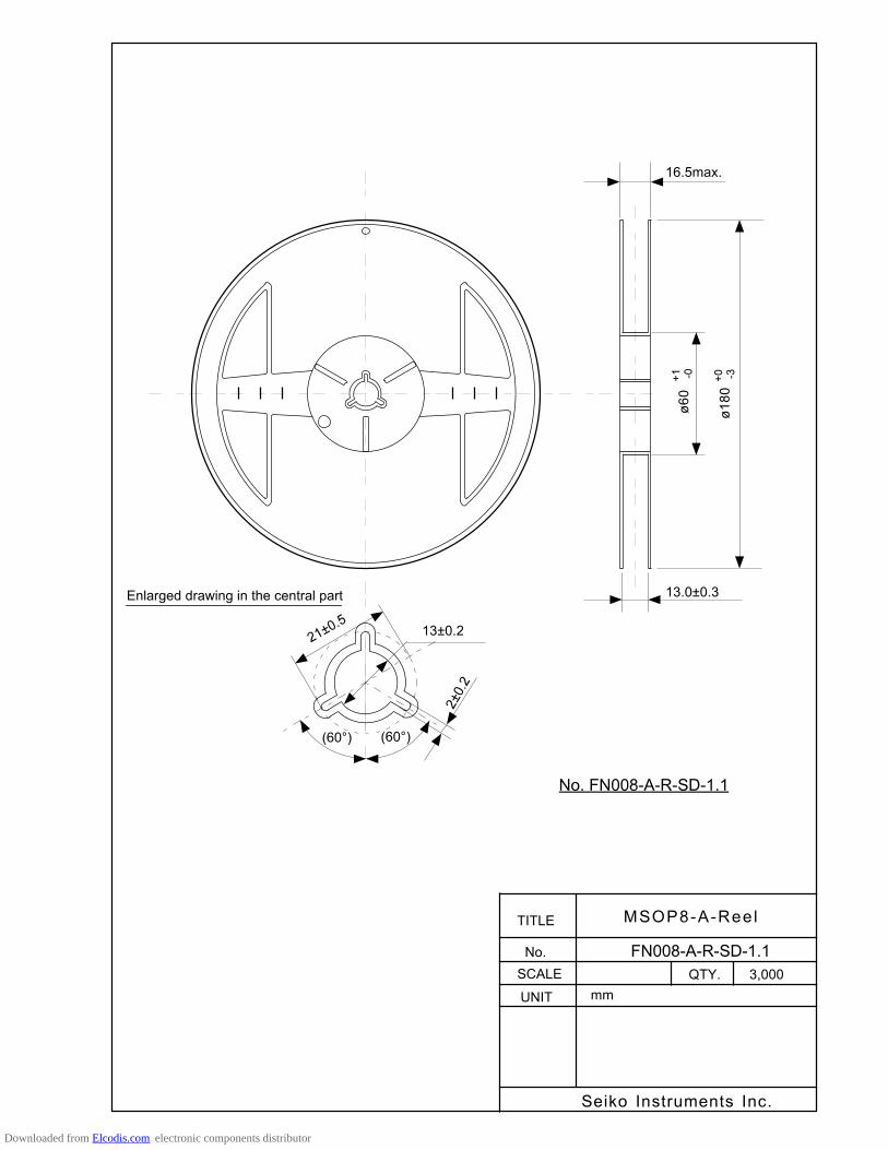
Rev.3.3_00 BATTERY PROTECTION IC FOR 1-SERIAL TO 4-SERIAL-CELL PACK (SECONDARY PROTECTION) S-8244 Series Seiko Instruments Inc. 1 The S-8244 Series is used for secondary protection of lithium-ion batteries with from one to four cells, and incorporates a high- precision voltage detector circuit and a delay circuit. Short-circuits between cells accommodate series connection of one to four cells. Features (1) Internal high-precision voltage detector circuit • Overcharge detection voltage range : 3.70 to 4.50 V : Accuracy of ± 25 mV (at +25 °C) (at a 5 mV/step) Accuracy of ± 50 mV (at -40 to +85 °C) • Hysteresis : 5 optional models available and selectable: 0.38±0.1 V, 0.25±0.07 V, 0.13±0.04 V, 0.045±0.02 V, None (2) High withstand voltage device : Absolute maximum rating : 26 V (3) Wide operating voltage range : 3.6 V to 24 V (refers to the range in which the delay circuit can operate normally after overvoltage is detected) (4) Delay time during detection : Can be set by an external capacitor. (5) Low current consumption : At 3.5 V for each cell : 3.0 µA max. (+25 °C) At 2.3 V for each cell : 2.4 µA max. (+25 °C) (6) Output logic and form : 4 types CMOS output active “H” CMOS output active “L” Pch open drain output active “L” Nch open drain output active “H” (only CMOS output for 0.045 V hysteresis models) (7) Lead-free products Applications • Lithium ion rechargeable battery packs (secondary protection) Packages Drawing code Package name Package Tape Reel Land SNT-8A PH008-A PH008-A PH008-A PH008-A 8-Pin MSOP FN008-A FN008-A FN008-A Downloaded from Elcodis.com electronic components distributor

Welcome message from author
This document is posted to help you gain knowledge. Please leave a comment to let me know what you think about it! Share it to your friends and learn new things together.
Transcript
Rev.3.3_00
BATTERY PROTECTION IC FOR 1-SERIAL TO 4-SERIAL-CELL PACK (SECONDARY PROTECTION) S-8244 Series
Seiko Instruments Inc. 1
The S-8244 Series is used for secondary protection of lithium-ion batteries with from one to four cells, and incorporates a high-precision voltage detector circuit and a delay circuit. Short-circuits between cells accommodate series connection of one to four cells.
Features (1) Internal high-precision voltage detector circuit
• Overcharge detection voltage range : 3.70 to 4.50 V : Accuracy of ± 25 mV (at +25 °C) (at a 5 mV/step) Accuracy of ± 50 mV (at -40 to +85 °C) • Hysteresis : 5 optional models available and selectable: 0.38±0.1 V, 0.25±0.07 V, 0.13±0.04 V, 0.045±0.02 V, None
(2) High withstand voltage device : Absolute maximum rating : 26 V (3) Wide operating voltage range : 3.6 V to 24 V (refers to the range in which the delay circuit can
operate normally after overvoltage is detected) (4) Delay time during detection : Can be set by an external capacitor. (5) Low current consumption : At 3.5 V for each cell : 3.0 µA max. (+25 °C)
At 2.3 V for each cell : 2.4 µA max. (+25 °C) (6) Output logic and form : 4 types
CMOS output active “H” CMOS output active “L” Pch open drain output active “L” Nch open drain output active “H” (only CMOS output for 0.045 V hysteresis models)
(7) Lead-free products
Applications • Lithium ion rechargeable battery packs (secondary protection)
Packages Drawing code Package name
Package Tape Reel Land SNT-8A PH008-A PH008-A PH008-A PH008-A
8-Pin MSOP FN008-A FN008-A FN008-A
Downloaded from Elcodis.com electronic components distributor
BATTERY PROTECTION IC FOR 1-SERIAL TO 4-SERIAL-CELL PACK (SECONDARY PROTECTION) S-8244 Series Rev.3.3_00
Seiko Instruments Inc. 2
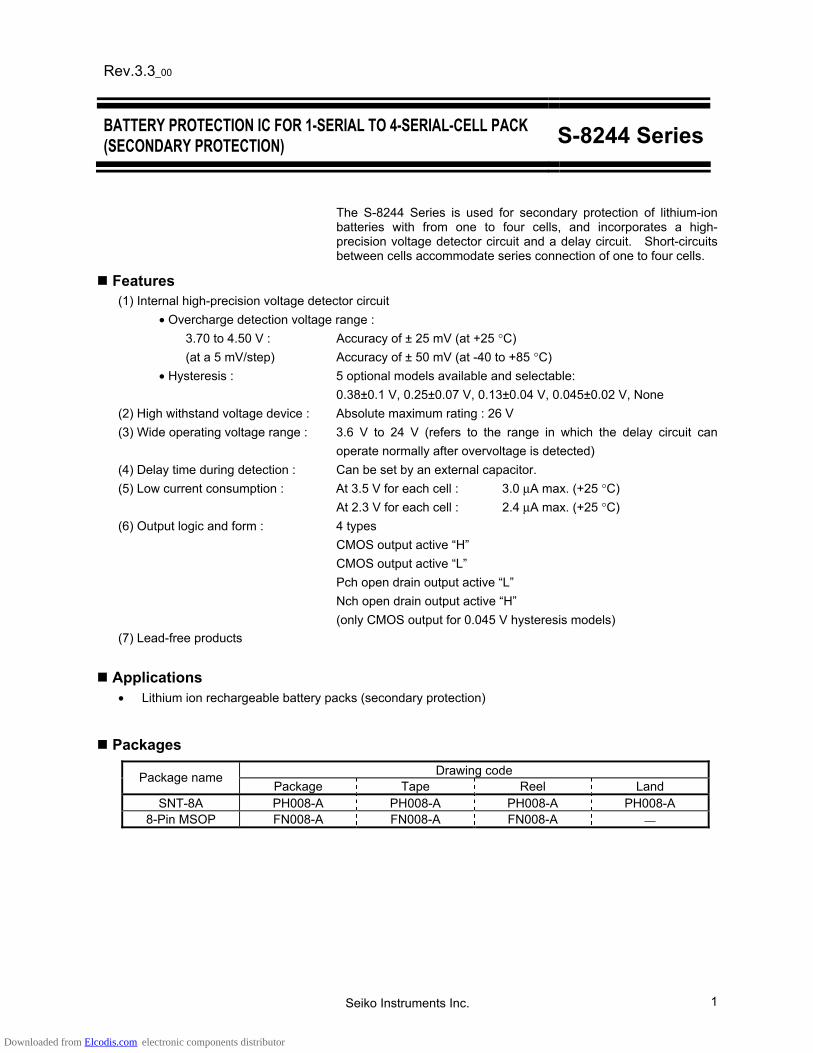
Block Diagram
VCC
ICT
VC2
VC1
-
+
CO
SENSE
VC3
Control logic
Overcharge detection comparator 4
Overcharge detection comparator 3
Overcharge detection comparator 2
Overcharge detection comparator 1
Reference voltage 4
Reference voltage 3
Reference voltage 2
Reference voltage 1
VSS
-
+
-
+
-
+
Overcharge detection delay circuit
Remark In the case of Nch open-drain output, only the Nch transistor will be
connected to the CO pin. In the case of Pch open-drain output, only the Pch transistor will be connected to the CO pin.
Figure 1
Downloaded from Elcodis.com electronic components distributor

BATTERY PROTECTION IC FOR 1-SERIAL TO 4-SERIAL-CELL PACK (SECONDARY PROTECTION) Rev.3.3_00 S-8244 Series
Seiko Instruments Inc. 3
Product Name Structure
1. Product Name
S-8244A xx xx - xxx xx G IC direction of tape specifications*1
TF: SNT-8A T2: 8-Pin MSOP
Product name (abbreviation)*2 Package abbreviation
PH: SNT-8A FN: 8-Pin MSOP
Serial code
Sequentially set from AA to ZZ
*1. Refer to the taping specifications at the end of this book. *2. Refer to the Product Name List.
Downloaded from Elcodis.com electronic components distributor

BATTERY PROTECTION IC FOR 1-SERIAL TO 4-SERIAL-CELL PACK (SECONDARY PROTECTION) S-8244 Series Rev.3.3_00
Seiko Instruments Inc. 4
2. Product Name List
(1) SNT-8A
Table 1
Product name/Item Overcharge
detection voltage [VCU]
Overcharge hysteresis voltage
[VCD] Output form
S-8244AAAPH-CEATFG 4.45 ± 0.025 V 0.38 ± 0.1 V CMOS output active “H” S-8244AABPH-CEBTFG 4.20 ± 0.025 V 0 V Nch open drain active “H” S-8244AAFPH-CEFTFG 4.35 ± 0.025 V 0.045 ± 0.02 V CMOS output active “H” S-8244AAGPH-CEGTFG 4.45 ± 0.025 V 0.045 ± 0.02 V CMOS output active “H” S-8244AAVPH-CEVTFG 4.275 ± 0.025 V 0.045 ± 0.02 V CMOS output active “H” S-8244AAYPH-CEYTFG 4.300 ± 0.025 V 0.25 ± 0.07 V CMOS output active “H” S-8244AAZPH-CEZTFG 4.280 ± 0.025 V 0.25 ± 0.07 V CMOS output active “H”
Remark Please contact our sales office for the products with the detection voltage value other than those specified above.
(2) 8-Pin MSOP
Table 2
Product name/Item Overcharge
detection voltage [VCU]
Overcharge hysteresis voltage
[VCD] Output form
S-8244AAAFN-CEAT2G 4.45 ± 0.025 V 0.38 ± 0.1 V CMOS output active “H” S-8244AABFN-CEBT2G 4.20 ± 0.025 V 0 V Nch open drain active “H” S-8244AACFN-CECT2G 4.115 ± 0.025 V 0.13 ± 0.04 V CMOS output active “H” S-8244AADFN-CEDT2G 4.20 ± 0.025 V 0 V Pch open drain active “L” S-8244AAEFN-CEET2G 4.225 ± 0.025 V 0 V Nch open drain active “H” S-8244AAFFN-CEFT2G 4.35 ± 0.025 V 0.045 ± 0.02 V CMOS output active “H” S-8244AAGFN-CEGT2G 4.45 ± 0.025 V 0.045 ± 0.02 V CMOS output active “H” S-8244AAHFN-CEHT2G 4.30 ± 0.025 V 0.25 ± 0.07 V CMOS output active “H” S-8244AAIFN-CEIT2G 4.40 ± 0.025 V 0.045 ± 0.02 V CMOS output active “H” S-8244AAJFN-CEJT2G 4.50 ± 0.025 V 0.38 ± 0.1 V CMOS output active “H” S-8244AAKFN-CEKT2G 4.475 ± 0.025 V 0.38 ± 0.1 V CMOS output active “H” S-8244AALFN-CELT2G 4.35 ± 0.025 V 0.25 ± 0.07 V CMOS output active “H” S-8244AAMFN-CEMT2G 4.30 ± 0.025 V 0.25 ± 0.07 V CMOS output active “L” S-8244AANFN-CENT2G 4.15 ± 0.025 V 0.25 ± 0.07 V CMOS output active “H” S-8244AAOFN-CEOT2G 4.25 ± 0.025 V 0.25 ± 0.07 V CMOS output active “H” S-8244AAPFN-CEPT2G 4.05 ± 0.025 V 0.25 ± 0.07 V CMOS output active “H” S-8244AAQFN-CEQT2G 4.15 ± 0.025 V 0 V Nch open drain active “H” S-8244AARFN-CERT2G 4.30 ± 0.025 V 0.25 ± 0.07 V Nch open drain active “H”
Remark Please contact our sales office department for the products with the detection voltage value other than those specified above.
Downloaded from Elcodis.com electronic components distributor

BATTERY PROTECTION IC FOR 1-SERIAL TO 4-SERIAL-CELL PACK (SECONDARY PROTECTION) Rev.3.3_00 S-8244 Series
Seiko Instruments Inc. 5
Pin Configurations
Table 3 Pin No. Symbol Description 1 CO FET gate connection pin for charge control
2 ICT Capacitor connection pin for overcharge detection delay
3 VSS Negative power input pin Negative voltage connection pin of Battery 4
4 VC3 Negative voltage connection pin of Battery 3 Positive voltage connection pin of Battery 4
5 VC2 Negative voltage connection pin of Battery 2 Positive voltage connection pin of Battery 3
6 VC1 Negative voltage connection pin of Battery 1 Positive voltage connection pin of Battery 2
SNT-8A Top view
1 2 3 4
COICT
VSSVC3
6
8 7
5
VCC SENSE VC1 VC2
7 SENSE Positive voltage connection pin of Battery 1 Figure 2 8 VCC Positive power input pin
Table 4 Pin No. Symbol Description 1 VCC Positive power input pin
2 SENSE Positive voltage connection pin of Battery 1
3 VC1 Negative voltage connection pin of Battery 1 Positive voltage connection pin of Battery 2
4 VC2 Negative voltage connection pin of Battery 2 Positive voltage connection pin of Battery 3
5 VC3 Negative voltage connection pin of Battery 3 Positive voltage connection pin of Battery 4
6 VSS Negative power input pin Negative voltage connection pin of Battery 4
8-Pin MSOP Top view
VCCSENSE
VC1VC2
CO ICT VSS
VC3 3
2
4
1 8
67
5
7 ICT Capacitor connection pin for overcharge detection delay
Figure 3 8 CO FET gate connection pin for charge control
Downloaded from Elcodis.com electronic components distributor
BATTERY PROTECTION IC FOR 1-SERIAL TO 4-SERIAL-CELL PACK (SECONDARY PROTECTION) S-8244 Series Rev.3.3_00
Seiko Instruments Inc. 6
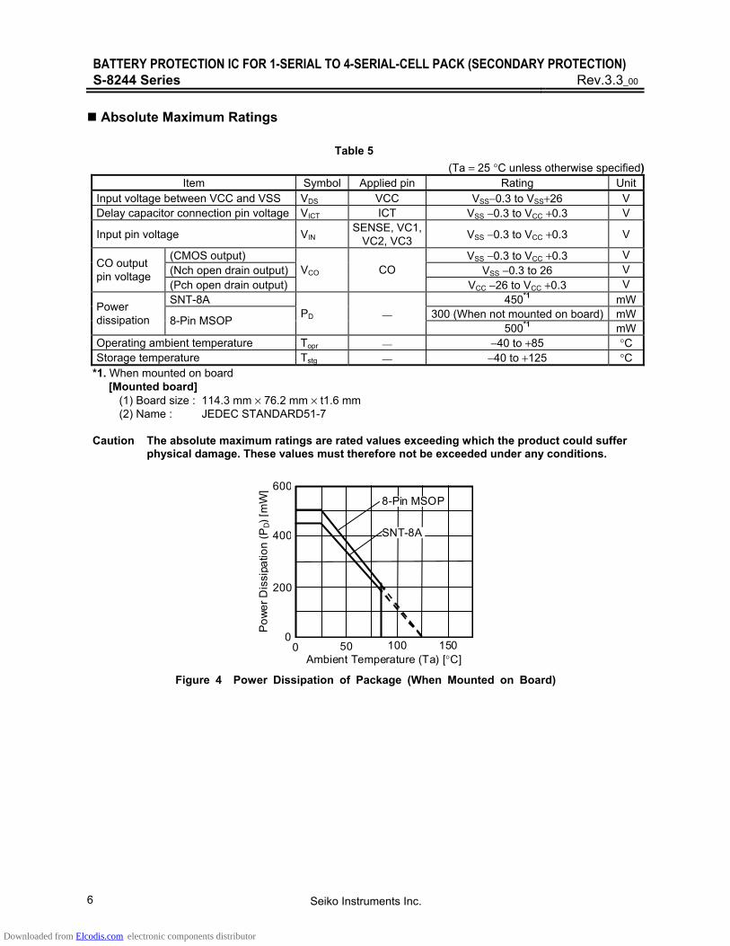
Absolute Maximum Ratings
Table 5 (Ta = 25 °C unless otherwise specified)
Item Symbol Applied pin Rating Unit Input voltage between VCC and VSS VDS VCC VSS−0.3 to VSS+26 V Delay capacitor connection pin voltage VICT ICT VSS −0.3 to VCC +0.3 V
Input pin voltage VIN SENSE, VC1, VC2, VC3 VSS −0.3 to VCC +0.3 V
(CMOS output) VSS −0.3 to VCC +0.3 V (Nch open drain output) VSS −0.3 to 26 V CO output
pin voltage (Pch open drain output)
VCO CO VCC −26 to VCC +0.3 V
SNT-8A 450*1 mW 300 (When not mounted on board) mW Power
dissipation 8-Pin MSOP PD 500*1 mW
Operating ambient temperature Topr −40 to +85 °C Storage temperature Tstg −40 to +125 °C
*1. When mounted on board [Mounted board] (1) Board size : 114.3 mm × 76.2 mm × t1.6 mm (2) Name : JEDEC STANDARD51-7
Caution The absolute maximum ratings are rated values exceeding which the product could suffer physical damage. These values must therefore not be exceeded under any conditions.
0 50 100 1500
Pow
er D
issi
patio
n (P
D) [m
W]
Ambient Temperature (Ta) [°C]
400
600
200
8-Pin MSOP
SNT-8A
Figure 4 Power Dissipation of Package (When Mounted on Board)
Downloaded from Elcodis.com electronic components distributor

BATTERY PROTECTION IC FOR 1-SERIAL TO 4-SERIAL-CELL PACK (SECONDARY PROTECTION) Rev.3.3_00 S-8244 Series
Seiko Instruments Inc. 7
Electrical Characteristics Table 6
(Ta = 25 °C unless otherwise specified)
Item Symbol Conditions Min. Typ. Max. Unit Test conditions
Test circuit
DETECTION VOLTAGE
Overcharge detection voltage 1 *1 VCU1 3.7 to 4.5 V Adjustment VCU1 −0.025 VCU1
VCU1 +0.025 V 1 1
Overcharge detection voltage 2 *1 VCU2 3.7 to 4.5 V Adjustment VCU2 −0.025 VCU2
VCU2 +0.025 V 2 1
Overcharge detection voltage 3 *1 VCU3 3.7 to 4.5 V Adjustment VCU3 −0.025 VCU3
VCU3 +0.025 V 3 1
Overcharge detection voltage 4 *1 VCU4 3.7 to 4.5 V Adjustment VCU4 −0.025 VCU4
VCU4 +0.025 V 4 1
Overcharge hysteresis voltage 1 *2 VCD1 0.28 0.38 0.48 V 1 1 Overcharge hysteresis voltage 2 *2 VCD2 0.28 0.38 0.48 V 2 1 Overcharge hysteresis voltage 3 *2 VCD3 0.28 0.38 0.48 V 3 1 Overcharge hysteresis voltage 4 *2 VCD4 0.28 0.38 0.48 V 4 1 Detection voltage temperature coefficient *3 TCOE Ta=−40 to +85 °C −0.4 0.0 +0.4 mV/°C
DELAY TIME Overcharge detection delay time tCU C=0.1 µF 1.0 1.5 2.0 s 5 2 OPERATING VOLTAGE Operating voltage between VCC and VSS *4 VDSOP 3.6 24 V
CURRENT CONSUMPTION Current consumption during normal operation IOPE V1=V2=V3=V4=3.5 V 1.5 3.0 µA 6 3
Current consumption at power down IPDN V1=V2=V3=V4=2.3 V 1.2 2.4 µA 6 3 VC1 sink current IVC1 V1=V2=V3=V4=3.5 V −0.3 0.3 µA 6 3 VC2 sink current IVC2 V1=V2=V3=V4=3.5 V −0.3 0.3 µA 6 3 VC3 sink current IVC3 V1=V2=V3=V4=3.5 V −0.3 0.3 µA 6 3 OUTPUT VOLTAGE*5
CO “H” voltage VCO(H) at IOUT = 10 µA VCC
−0.05 V 7 4
CO “L” voltage VCO(L) at IOUT = 10 µA VSS
+0.05 V 7 4
*1. ±50 mV when Ta = −40 to +85 °C. *2. 0.25±0.07 V, 0.13±0.04 V, 0.045±0.02 V except for 0.38 V hysteresis models. *3. Overcharge detection voltage or overcharge hysteresis voltage. *4. After detecting the overcharge, the delay circuit operates normally in the range of operating voltage. *5. Output logic and CMOS or open drain output can be selected.
Downloaded from Elcodis.com electronic components distributor

BATTERY PROTECTION IC FOR 1-SERIAL TO 4-SERIAL-CELL PACK (SECONDARY PROTECTION) S-8244 Series Rev.3.3_00
Seiko Instruments Inc. 8
Test Circuits
(1) Test Condition 1, Test Circuit 1
Conditions: • Set switches 1 and 2 to OFF for CMOS output models. • Set switch 1 to ON and switch 2 to OFF for Nch open drain models. • Set switch 1 to OFF and switch 2 to ON for Pch open drain models. Definitions: • Set V1, V2, V3 and V4 to 3.5 V and gradually increase V1:
Overcharge detection voltage 1 (VCU1) is defined as V1 voltage when CO is turned to “H” (for CMOS output active “H” or Nch open drain) or “L” (for CMOS output active “L” or Pch open drain).
• Next, gradually decrease V1: Overcharge hysteresis voltage (VCD1) is defined as a difference between VCU1 and V1 when CO is turned to “L” (for CMOS output active “H” or Nch open drain) or “H” (for CMOS output active “L” or Pch open drain).
(2) Test Condition 2, Test Circuit 1
Conditions: • Set switches 1 and 2 to OFF for CMOS output models. • Set switch 1 to ON and switch 2 to OFF for Nch open drain models. • Set switch 1 to OFF and switch 2 to ON for Pch open drain models. Definitions: • Set V1, V2, V3 and V4 to 3.5 V and gradually increase V2.
Overcharge detection voltage 2 (VCU2) is defined as V2 voltage when CO is turned to “H” (for CMOS output active “H” or Nch open drain) or “L” (for CMOS output active “L” or Pch open drain).
• Next, gradually decrease V2. Overcharge hysteresis voltage (VCD2) is defined as a difference between VCU2 and V2 when CO is turned to “L” (for CMOS output active “H” or Nch open drain) or “H” (for CMOS output active “L” or Pch open drain).
(3) Test Condition 3, Test Circuit 1
Conditions: • Set switches 1 and 2 to OFF for CMOS output models. • Set switch 1 to ON and switch 2 to OFF for Nch open drain models. • Set switch 1 to OFF and switch 2 to ON for Pch open drain models. Definitions: • Set V1, V2, V3 and V4 to 3.5 V and gradually increase V3.
Overcharge detection voltage 3 (VCU3) is defined as V3 voltage when CO is turned to “H” (for CMOS output active “H” or Nch open drain) or “L” (for CMOS output active “L” or Pch open drain).
• Next gradually decrease V3. Overcharge hysteresis voltage (VCD3) is defined as a difference between VCU3 and V3 when CO is turned to “L” (for CMOS output active “H” or Nch open drain) or “H” (for CMOS output active “L” or Pch open drain).
Downloaded from Elcodis.com electronic components distributor

BATTERY PROTECTION IC FOR 1-SERIAL TO 4-SERIAL-CELL PACK (SECONDARY PROTECTION) Rev.3.3_00 S-8244 Series
Seiko Instruments Inc. 9
(4) Test Condition 4, Test Circuit 1
Conditions: • Set switches 1 and 2 to OFF for CMOS output models. • Set switch 1 to ON and switch 2 to OFF for Nch open drain models. • Set switch 1 to OFF and switch 2 to ON for Pch open drain models. Definitions: • Set V1, V2, V3 and V4 to 3.5 V and gradually increase V4.
Overcharge detection voltage 4 (VCU4) is defined as V4 voltage when CO is turned to “H” (for CMOS output active “H” or Nch open drain) or “L” (for CMOS output active “L” or Pch open drain).
• Next, gradually decrease V4. Overcharge hysteresis voltage (VCD4) is defined as a difference between VCU4 and V4 when CO is turned to “L” (for CMOS output active “H” or Nch open drain) or “H” (for CMOS output active “L” or Pch open drain).
(5) Test Condition 5, Test Circuit 2
Conditions: • Set switches 1 and 2 to OFF for CMOS output models. • Set switch 1 to ON and switch 2 to OFF for Nch open drain models. • Set switch 1 to OFF and switch 2 to ON for Pch open drain models. Definition: • Set V1, V2, V3 and V4 to 3.5 V and momentarily rise V1 to 4.7 V within 10 µs.
Overcharge detection delay time (tCU) is the period from when V1 goes 4.7 V to when CO is turned to “H” (for CMOS output active “H” or Nch open drain) or “L” (for CMOS output active “L” or Pch open drain).
(6) Test Condition 6, Test Circuit 3
Conditions:
• Set V1, V2, V3 and V4 to 2.3 V. • Measure current consumption (I1). Definition:
• The current consumption (I1) is defined as current consumption at power down (IPDN). Conditions: • Set V1, V2, V3 and V4 to 3.5 V. • Measure current consumption I1, I2, I3, and I4. Definition: •The current consumption (I1) is defined as current consumption during normal operation (IOPE), the current consumption (I2) as VC1 sink current (IVC1), the current consumption (I3) as VC2 sink current (IVC2), and the current consumption (I4) as VC3 sink current (IVC3), respectively.
Downloaded from Elcodis.com electronic components distributor

BATTERY PROTECTION IC FOR 1-SERIAL TO 4-SERIAL-CELL PACK (SECONDARY PROTECTION) S-8244 Series Rev.3.3_00
Seiko Instruments Inc. 10
(7) Test Condition 7, Test Circuit 4
Conditions: • Set switch 1 to OFF and switch 2 to ON. Definitions: • Set V1, V2, V3 and V4 to 4.6 V and gradually decrease V6 from VCC (for CMOS output active “H”
models). V6 voltage is defined as VCO (H) when I2 (= -10 µA) flows.
• Set V1, V2, V3 and V4 to 3.5 V and gradually decrease V6 from VCC (for CMOS output active “L” or Pch open drain models). V6 voltage is defined as VCO (H) when I2 (= -10 µA) flows.
• Set V1, V2, V3 and V4 to 4.6 V and gradually increase V6 from 0 V (for CMOS output active “L” models). V6 voltage is defined as VCO (L) when I2 (= 10 µA) flows.
• Set V1, V2, V3 and V4 to 3.5 V and gradually increase V6 from 0 V (for CMOS output active “H” or Nch open drain models). V6 voltage is defined as VCO (L) when I2 (= 10 µA) flows.
10 MΩ
10 MΩ
V1
V2
V3
V4
SW2
SW1 S-8244
VCC
SENSE
VC1
VC2
CO
ICT
VSS
VC3
V
10 MΩ
10 MΩ
V1
V2
V3
V4
SW2
SW1 S-8244
VCC
SENSE
VC1
VC2
CO
ICT
VSS
VC3
0.1 µF V
Test Circuit 1
Test Circuit 2
V1
V2
V3
V4
S-8244 VCC
SENSE
VC1
VC2
CO
ICT
VSS
VC3
I1 I2
I3 I4
V5
V1
V2
V3
V4
SW2
SW1 S-8244
VCC
SENSE
VC1
VC2
CO
ICT
VSS
VC3 V6
I2
I1
V
Test Circuit 3
Test Circuit 4
Figure 5
Downloaded from Elcodis.com electronic components distributor

BATTERY PROTECTION IC FOR 1-SERIAL TO 4-SERIAL-CELL PACK (SECONDARY PROTECTION) Rev.3.3_00 S-8244 Series
Seiko Instruments Inc. 11
Operation
Overcharge Detection CO is turned to “H” (for CMOS output active “H” or Nch open drain models) or “L” (for CMOS output active “L” or Pch open drain models) when the voltage of one of the batteries exceeds the overcharge detection voltage (VCU) during charging under normal conditions beyond the overcharge detection delay time (tCU). This state is called “overcharge.” Attaching FET to the CO pin provides charge control and a second protection. At that time, the overcharge state is maintained until the voltage of all batteries decreases from the overcharge detection voltage (VCU) by the equivalent to the overcharge hysteresis voltage (VCD).
Delay Circuit The delay circuit rapidly charges the capacitor connected to the delay capacitor connection pin up to a specified voltage when the voltage of one of the batteries exceeds the overcharge detection voltage (VCU). Then, the delay circuit gradually discharges the capacitor at 100 nA and inverts the CO output when the voltage at the delay capacitor connection pin goes below a specified level. Overcharge detection delay time (tCU) varies depending upon the external capacitor.
Each delay time is calculated using the following equation.
Min. Typ. Max. tCU[s] = Delay Coefficient (10, 15, 20) × CICT [µF]
Because the delay capacitor is rapidly charged, the smaller the capacitance, the larger the difference between the maximum voltage and the specified value of delay capacitor pin (ICT pin). This will cause a deviation between the calculated delay time and the resultant delay time. Also, delay time is internally set in this IC to prevent the CO output from inverting until the charge to delay capacitor pin is reached to the specified voltage. If large capacitance is used, output may be enabled without delay time because charge is disabled within the internal delay time. Please note that the maximum capacitance connected to the delay capacitor pin (ICT pin) is 1 µF.
Downloaded from Elcodis.com electronic components distributor

BATTERY PROTECTION IC FOR 1-SERIAL TO 4-SERIAL-CELL PACK (SECONDARY PROTECTION) S-8244 Series Rev.3.3_00
Seiko Instruments Inc. 12
Timing Chart
VCU Battery voltage
VSS
CO pin voltage
VCC
CO pin voltage
VSS
Delay
VSS
ICT pin voltage
VCC
CMOS output active “H” and Nch open drain models
CMOS output active “L” and Pch open drain models
VCD V1 battery V2 battery V3 battery V4 battery
VSS
Figure 6
Downloaded from Elcodis.com electronic components distributor

BATTERY PROTECTION IC FOR 1-SERIAL TO 4-SERIAL-CELL PACK (SECONDARY PROTECTION) Rev.3.3_00 S-8244 Series
Seiko Instruments Inc. 13
Battery Protection IC Connection Example (1) Connection Example 1
SC PROTECTOR
EB-
CVCC
CICT
C1
C2
C3
C4
EB+
R1
R2
R3
R4
BAT1
BAT2
BAT3
BAT4
RVCC
FET
SENSE
VC1
VC2
VC3
VSS
VCC
ICT
CO
Figure 7
Table 7 Constants for External Components 1 Symbol Min. Typ. Max. Unit
R1 to R4 0 1 k 10 k Ω C1 to C4 0 0.1 1 µF
RVCC 0 100 1 k Ω CVCC 0 0.1 1 µF CICT 0 0.1 1 µF
Caution1. The above constants may be changed without notice.
2. It has not been confirmed whether the operation is normal or not in circuits other than the above example of connection. In addition, the example of connection shown above and the constant do not guarantee proper operation. Perform through evaluation using the actual application to set the constant.
3. In the case of Nch open drain output, pull up CO pin by external resistor.
[For SC PROTECTOR, contact] Sony Chemicals Corporation Electronic Devices Business Group 1-11-2 Osaki, Shinagawa-ku, Tokyo, 141-0032 Japan TEL: +81-3-5435-3943 FAX: +81-3-5435-3072
Downloaded from Elcodis.com electronic components distributor

BATTERY PROTECTION IC FOR 1-SERIAL TO 4-SERIAL-CELL PACK (SECONDARY PROTECTION) S-8244 Series Rev.3.3_00
Seiko Instruments Inc. 14
(2) Connection Example 2
SC PROTECTOR
EB-
CVCC
CICT
C1
C2
C3
C4
EB+
R1
R2
R3
R4
BAT1
BAT2
BAT3
BAT4
RVCC
FET
SENSE
VC1
VC2
VC3
VSS
VCC
ICT
CO
Figure 8
Table 8 Constants for External Components 2
Symbol Min. Typ. Max. Unit R1 to R4 0 1 k 10 k Ω C1 to C4 0 0.1 1 µF
RVCC 0 100 1 k Ω CVCC 0 0.1 1 µF CICT 0 0.1 1 µF
Caution1. The above constants may be changed without notice.
2. It has not been confirmed whether the operation is normal or not in circuits other than the above example of connection. In addition, the example of connection shown above and the constant do not guarantee proper operation. Perform through evaluation using the actual application to set the constant.
3. In the case of Nch open drain output, pull up CO pin by external resistor.
Downloaded from Elcodis.com electronic components distributor

BATTERY PROTECTION IC FOR 1-SERIAL TO 4-SERIAL-CELL PACK (SECONDARY PROTECTION) Rev.3.3_00 S-8244 Series
Seiko Instruments Inc. 15
(3) Connection Example 3 (for 3-cells)
SC PROTECTOR
EB-
CVCC
CICT
C1
C2
C3
EB+
R1
R2
R3
BAT1
BAT2
BAT3
RVCC
FET
SENSE
VC1
VC2
VC3
VSS
VCC
ICT
CO
Figure 9
Table 9 Constants for External Components 3 Symbol Min. Typ. Max. Unit
R1 to R3 0 1 k 10 k Ω C1 to C3 0 0.1 1 µF
RVCC 0 100 1 k Ω CVCC 0 0.1 1 µF CICT 0 0.1 1 µF
Caution1. The above constants may be changed without notice.
2. It has not been confirmed whether the operation is normal or not in circuits other than the above example of connection. In addition, the example of connection shown above and the constant do not guarantee proper operation. Perform through evaluation using the actual application to set the constant.
3. In the case of Nch open drain output, pull up CO pin by external resistor.
Downloaded from Elcodis.com electronic components distributor

BATTERY PROTECTION IC FOR 1-SERIAL TO 4-SERIAL-CELL PACK (SECONDARY PROTECTION) S-8244 Series Rev.3.3_00
Seiko Instruments Inc. 16
(4) Connection Example 4 (for 2-cells)
SC PROTECTOR
EB-
CVCC
CICT
C1
C2
EB+
R1
R2
BAT1
BAT2
RVCC
FET
SENSE
VC1
VC2
VC3
VSS
VCC
ICT
CO
Figure 10
Table 10 Constants for External Components 4 Symbol Min. Typ. Max. Unit R1, R2 0 1 k 10 k Ω C1, C2 0 0.1 1 µF RVCC 0 100 1 k Ω CVCC 0 0.1 1 µF CICT 0 0.1 1 µF
Caution1. The above constants may be changed without notice.
2. It has not been confirmed whether the operation is normal or not in circuits other than the above example of connection. In addition, the example of connection shown above and the constant do not guarantee proper operation. Perform through evaluation using the actual application to set the constant.
3. In the case of Nch open drain output, pull up CO pin by external resistor.
Downloaded from Elcodis.com electronic components distributor

BATTERY PROTECTION IC FOR 1-SERIAL TO 4-SERIAL-CELL PACK (SECONDARY PROTECTION) Rev.3.3_00 S-8244 Series
Seiko Instruments Inc. 17
(5) Connection Example 5 (for 1-cell)
EB-
CVCC
CICT
C1
EB+
R1 BAT1
RVCC
FET
SENSE
VC1
VC2
VC3
VSS
VCC
ICT
CO
SC PROTECTOR
Figure 11
Table 11 Constants for External Components 5 Symbol Min. Typ. Max. Unit
R1 0 1 k 10 k Ω C1 0 0.1 1 µF
RVCC 0 100 1 k Ω CVCC 0 0.1 1 µF CICT 0 0.1 1 µF
Caution1. The above constants may be changed without notice.
2. It has not been confirmed whether the operation is normal or not in circuits other than the above example of connection. In addition, the example of connection shown above and the constant do not guarantee proper operation. Perform through evaluation using the actual application to set the constant.
3. In the case of Nch open drain output, pull up CO pin by external resistor.
Downloaded from Elcodis.com electronic components distributor

BATTERY PROTECTION IC FOR 1-SERIAL TO 4-SERIAL-CELL PACK (SECONDARY PROTECTION) S-8244 Series Rev.3.3_00
Seiko Instruments Inc. 18
Precautions • This IC charges the delay capacitor through the delay capacitor pin (ICT pin) immediately when the
voltage of one of batteries V1 to V4 reaches the overcharge voltage. Therefore, setting the resistor connected to the VCC pin to any value greater than the recommended level causes a reduction in the IC power supply voltage because of charge current of the delay capacitor. This may lead to a malfunction. Set up the resistor NOT to exceed the typical value. If you change the resistance, please consult us.
• DO NOT connect any of overcharged batteries. Even if only one overcharged battery is connected to this IC, the IC detects overcharge, then charge current flows to the delay capacitor through the parasitic diode between pins where the battery is not connected yet. This may lead to a malfunction. Please perform sufficient evaluation in the case of use. Depending on an application circuit, even when the fault charge battery is not contained, the connection turn of a battery may be restricted in order to prevent the output of CO detection pulse at the time of battery connection.
VCU
Battery voltage
Setting voltage
VCC
CO pin voltage
VSS
VSS
ICT pin voltage
CMOS output active “H” and Nch open drain models
VCD V1 battery V2 battery V3 battery V4 battery
Internal delay
Delay
CICT low
CICT high
CICT low CICT high
VSS
• In this IC, the output logic of the CO pin is inverted after several milliseconds of internal delay if this IC is under the overcharge condition even ICT pin is either “VSS-short circuit,” “VDD-short circuit” or “Open” status.
• Any position from V1 to V4 can be used when applying this IC for a one to three-cell battery. However, be sure to short circuit between pins not in use (SENSE-VC1, VC1-VC2, VC2-VC3, or VC3-VSS).
• The application conditions for the input voltage, output voltage, and load current should not exceed the package power dissipation.
• Do not apply an electrostatic discharge to this IC that exceeds the performance ratings of the built-in electrostatic protection circuit.
• SII claims no responsibility for any and all disputes arising out of or in connection with any infringement of the products including this IC upon patents owned by a third party.
Downloaded from Elcodis.com electronic components distributor

BATTERY PROTECTION IC FOR 1-SERIAL TO 4-SERIAL-CELL PACK (SECONDARY PROTECTION) Rev.3.3_00 S-8244 Series
Seiko Instruments Inc. 19
Characteristics (Typical Data)
1. Detection Voltage vs. Temperature Overcharge Detection Voltage vs. Temperature
Overcharge Release Voltage vs. Temperature
4.35
4.45
4.55
-40 -20 0 20 40 60 80 100 Ta(°C)
V CU(V
)
S-8244AAAFN VCU = 4.45(V)
3.97
4.07
4.17
-40 -20 0 20 40 60 80 100Ta(°C)
V CU-V
CD(V
)
S-8244AAAFN VCD=0.38(V)
2. Current Consumption vs. Temperature Current Consumption during Normal Operation vs. Temperature
Current Consumption at Power Down vs. Temperature
I CP
E(µ
A)
0
1
2
3
-40 -20 0 20 40 60 80 100 Ta( ° C)
S-8244AAAFN VCC = 14.0(V)
0
1
2
3
-40 -20 0 20 40 60 80 100 Ta( ° C)
I PD
N(µ
A)
S-8244AAAFN VCC = 9.2(V)
3. Delay Time vs. Temperature Overcharge Detection Delay Time vs. Temperature
0
1
2
3
-40 -20 0 20 40 60 80 100 Ta( ° C)
t CU(s
)
S-8244AAAFN VCC = 15.2(V)
Caution Please design all applications of the S-8244 Series with safety in mind.
Downloaded from Elcodis.com electronic components distributor

!!!"#$%
"&!!"!%!
"&!!"!%!
'!
(
Downloaded from Elcodis.com electronic components distributor

"&!!!%!
!!!) )*
"&!!!%!
+,,
-'
!
-
(
(
.
Downloaded from Elcodis.com electronic components distributor

)/
-
0(.1 0(.1
2)3,,)435 )2*)
67
"&!!8!%!
!!!82
"&!!8!%!
9
Downloaded from Elcodis.com electronic components distributor

!!!),8 ,)
"&!!!%!
"&!!!%!
) :)354*),5*) )3* =2& 4@9 5)5*) )3)>=*),, 55 ),=>52 *3), <) 2, 5*)= )5*) )3, 5)@5), <<
Downloaded from Elcodis.com electronic components distributor

!"#$$#%&'
($$#$'$
($$#$'$
Downloaded from Elcodis.com electronic components distributor

!"#$$) )*
( ++
($$$'$
($$$'$
Downloaded from Elcodis.com electronic components distributor
),
-. /
012012
3)4 ++)546 )3*)
!"#$$7 3
($$7$'$
($$7$'$
Downloaded from Elcodis.com electronic components distributor

• The information described herein is subject to change without notice.• Seiko Instruments Inc. is not responsible for any problems caused by circuits or diagrams described herein
whose related industrial properties, patents, or other rights belong to third parties. The application circuitexamples explain typical applications of the products, and do not guarantee the success of any specificmass-production design.
• When the products described herein are regulated products subject to the Wassenaar Arrangement or otheragreements, they may not be exported without authorization from the appropriate governmental authority.
• Use of the information described herein for other purposes and/or reproduction or copying without theexpress permission of Seiko Instruments Inc. is strictly prohibited.
• The products described herein cannot be used as part of any device or equipment affecting the humanbody, such as exercise equipment, medical equipment, security systems, gas equipment, or any apparatusinstalled in airplanes and other vehicles, without prior written permission of Seiko Instruments Inc.
• Although Seiko Instruments Inc. exerts the greatest possible effort to ensure high quality and reliability, thefailure or malfunction of semiconductor products may occur. The user of these products should thereforegive thorough consideration to safety design, including redundancy, fire-prevention measures, andmalfunction prevention, to prevent any accidents, fires, or community damage that may ensue.
Downloaded from Elcodis.com electronic components distributor
Related Documents