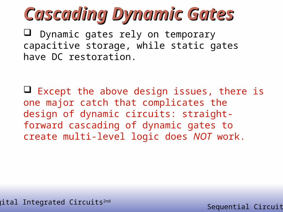
gital Integrated Circuits 2nd Sequential Circuit Cascading Dynamic Gates Cascading Dynamic Gates Dynamic gates rely on temporary capacitive storage, while static gates have DC restoration. Except the above design issues, there is one major catch that complicates the design of dynamic circuits: straight- forward cascading of dynamic gates to create multi-level logic does NOT work.

© Digital Integrated Circuits 2nd Sequential Circuits Cascading Dynamic Gates Dynamic gates rely on temporary capacitive storage, while static gates.
Dec 21, 2015
Welcome message from author
This document is posted to help you gain knowledge. Please leave a comment to let me know what you think about it! Share it to your friends and learn new things together.
Transcript
© Digital Integrated Circuits2nd
Sequential Circuits
Cascading Dynamic GatesCascading Dynamic Gates Dynamic gates rely on temporary capacitive storage, while static gates have DC restoration.
Except the above design issues, there is one major catch that complicates the design of dynamic circuits: straight-forward cascading of dynamic gates to create multi-level logic does NOT work.
© Digital Integrated Circuits2nd
Sequential Circuits
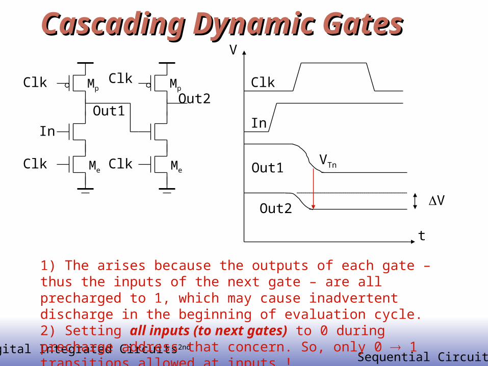
Cascading Dynamic GatesCascading Dynamic Gates
Clk
Clk
Out1
In
Mp
Me
Mp
Me
Clk
Clk
Out2
V
t
Clk
In
Out1
Out2V
VTn
1) The arises because the outputs of each gate – thus the inputs of the next gate – are all precharged to 1, which may cause inadvertent discharge in the beginning of evaluation cycle.2) Setting all inputs (to next gates) to 0 during precharge address that concern. So, only 0 1 transitions allowed at inputs !

© Digital Integrated Circuits2nd
Sequential Circuits
Domino Logic – NMOS dynamic gate Domino Logic – NMOS dynamic gate with static inverterwith static inverter
In1
In2 PDN
In3
Me
Mp
Clk
ClkOut1
In4 PDN
In5
Me
Mp
Clk
ClkOut2
Mkp
1 11 0
0 00 1
Additional advantage of introducing an inverter (low impedance of gate, smaller delay)
Bleeder device
© Digital Integrated Circuits2nd
Sequential Circuits
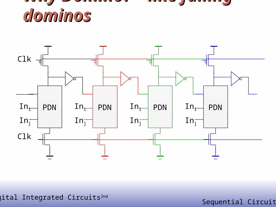
Why Domino? – like falling dominosWhy Domino? – like falling dominos
Clk
Clk
Ini PDN
Inj
Ini
Inj
PDN Ini PDN
Inj
Ini PDN
Inj
© Digital Integrated Circuits2nd
Sequential Circuits
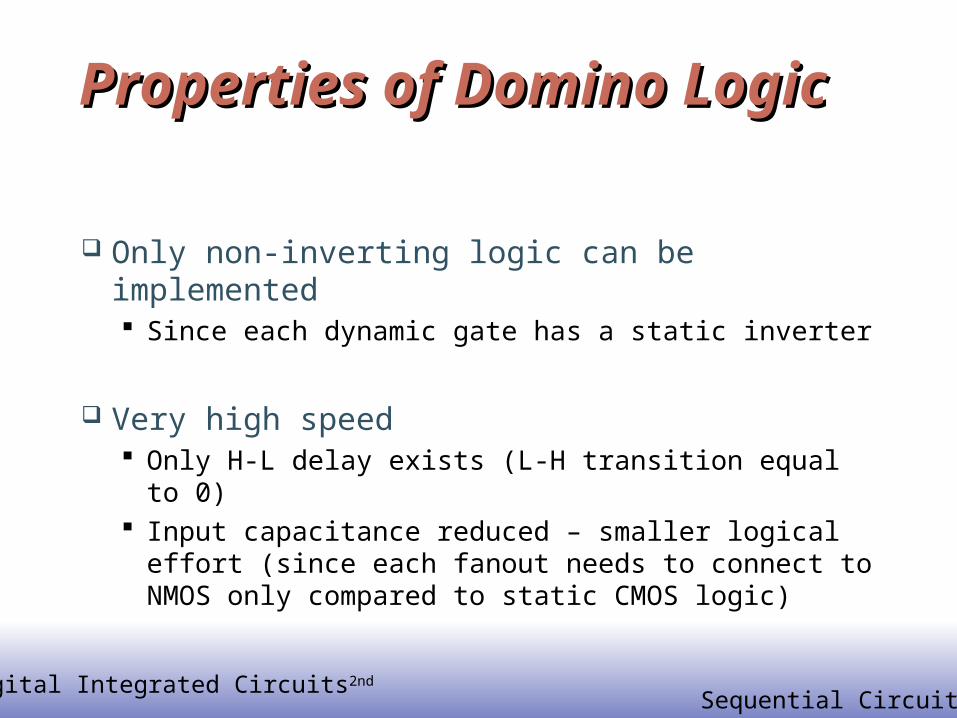
Properties of Domino LogicProperties of Domino Logic
Only non-inverting logic can be implemented Since each dynamic gate has a static inverter
Very high speed Only H-L delay exists (L-H transition equal to 0) Input capacitance reduced – smaller logical effort
(since each fanout needs to connect to NMOS only compared to static CMOS logic)
© Digital Integrated Circuits2nd
Sequential Circuits
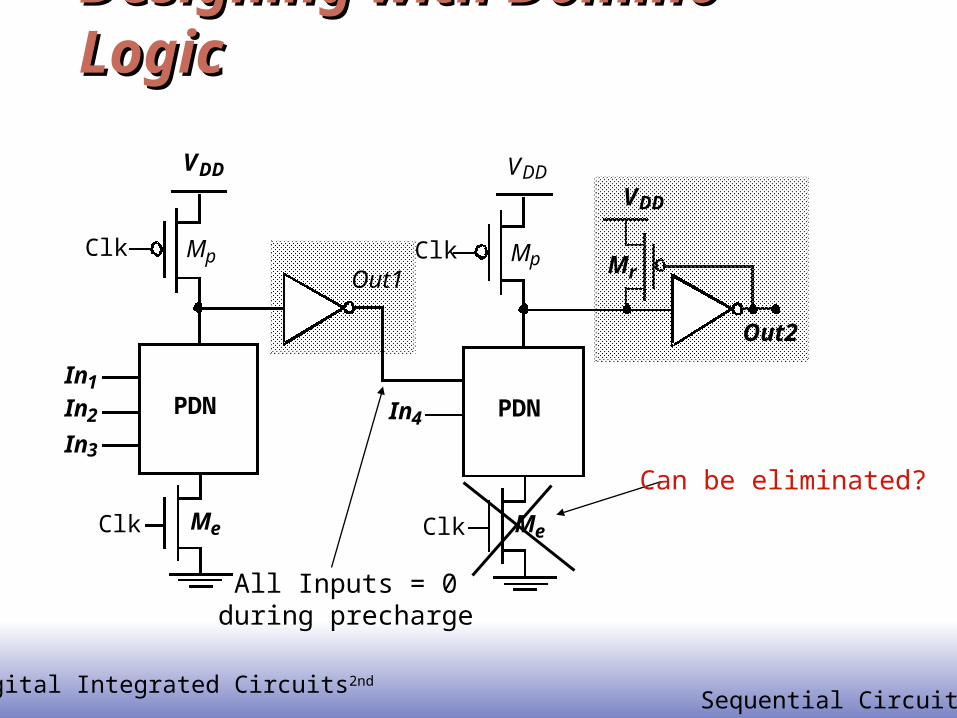
Designing with Domino LogicDesigning with Domino Logic
Mp
Me
VDD
PDN
Clk
In1In2In3
Out1
Clk
Mp
Me
VDD
PDN
Clk
In4
Clk
Out2
Mr
VDD
All Inputs = 0during precharge
Can be eliminated?

© Digital Integrated Circuits2nd
Sequential Circuits
Footless DominoFootless DominoVDD
Clk Mp
Out1
In1
1 0
VDD
Clk Mp
Out2
In2
VDD
Clk Mp
Outn
InnIn3
1 0
0 1 0 1 0 1
1) Without evaluation devices, when the first gate goes to precharge, the second gate has to wait for In2 to get to 0 since it fights against the precharge, which takes two inverter delays. More delay for later gates.
2) This also causes short circuit power consumption
© Digital Integrated Circuits2nd
Sequential Circuits
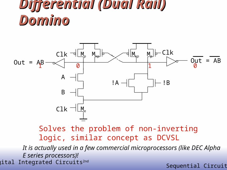
Differential (Dual Rail) DominoDifferential (Dual Rail) Domino
A
B
Me
Mp
Clk
ClkOut = AB
!A !B
MkpClk
Out = ABMkp Mp
Solves the problem of non-inverting logic, similar concept as DCVSL
1 0 1 0
It is actually used in a few commercial microprocessors (like DEC Alpha E series processors)!
© Digital Integrated Circuits2nd
Sequential Circuits
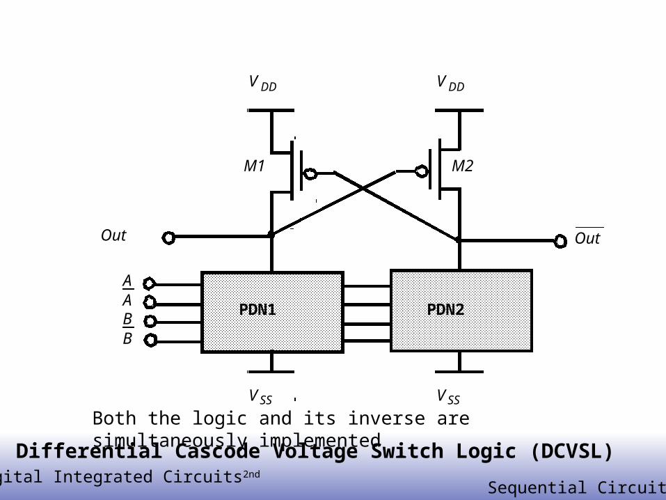
V DD
V SS
PDN1
Out
V DD
V SS
PDN2
Out
AABB
M1 M2
Differential Cascode Voltage Switch Logic (DCVSL)
Both the logic and its inverse are simultaneously implemented
© Digital Integrated Circuits2nd
Sequential Circuits
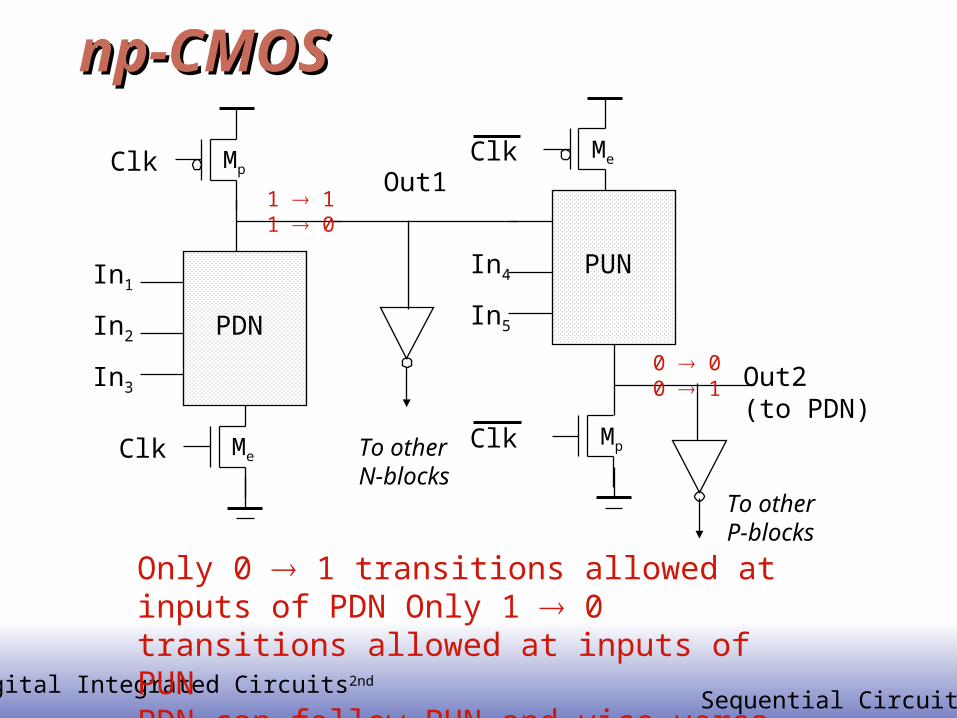
np-CMOSnp-CMOS
Only 0 1 transitions allowed at inputs of PDN Only 1 0 transitions allowed at inputs of PUNPDN can follow PUN and vice versa
In1
In2 PDN
In3
Me
Mp
Clk
ClkOut1
In4 PUN
In5
Me
MpClk
Clk
Out2(to PDN)
1 11 0
0 00 1
To other N-blocks
To other P-blocks
© Digital Integrated Circuits2nd
Sequential Circuits
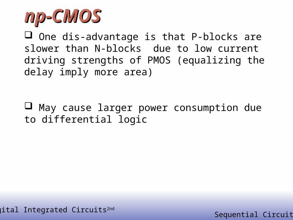
np-CMOSnp-CMOS One dis-advantage is that P-blocks are slower than N-blocks due to low current driving strengths of PMOS (equalizing the delay imply more area)
May cause larger power consumption due to differential logic
© Digital Integrated Circuits2nd
Sequential Circuits
Summary of logic stylesSummary of logic styles We have discussed Static complementary, Ratioed, Pass transistor and Dynamic logic styles
Which one to use strongly depends on the following factors: ease of design, robustness, area, power and speed.
No single style optimize all these metrics
Current trend is towards an increased use of complementary static CMOS logic style (somewhat due to the use of design automation tools at logic design level which requires that the logic be robust and complexity problem). Also, static CMOS is more amenable to voltage scaling.
© Digital Integrated Circuits2nd
Sequential Circuits
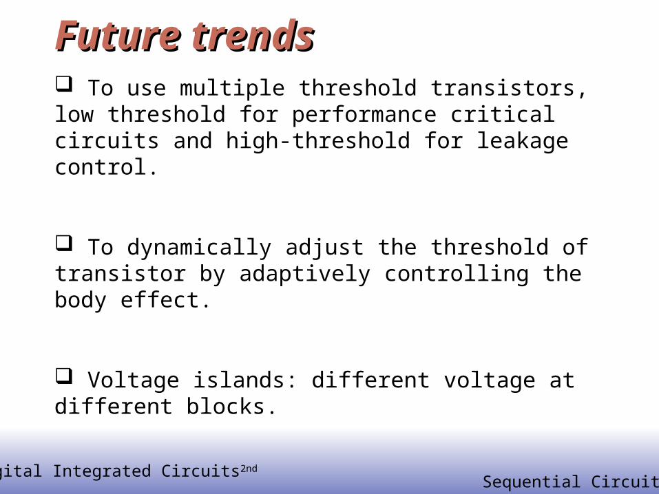
Future trendsFuture trends To use multiple threshold transistors, low threshold for performance critical circuits and high-threshold for leakage control.
To dynamically adjust the threshold of transistor by adaptively controlling the body effect.
Voltage islands: different voltage at different blocks.
© Digital Integrated Circuits2nd
Sequential Circuits
Layout techniques Layout techniques for complex gatesfor complex gates
© Digital Integrated Circuits2nd
Sequential Circuits
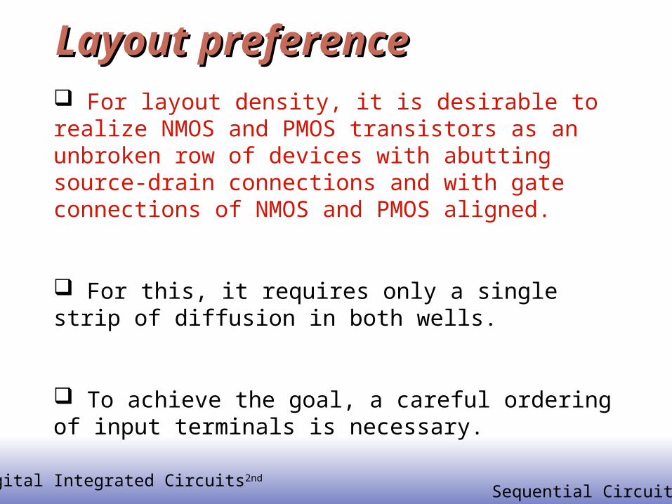
Layout preferenceLayout preference For layout density, it is desirable to realize NMOS and PMOS transistors as an unbroken row of devices with abutting source-drain connections and with gate connections of NMOS and PMOS aligned.
For this, it requires only a single strip of diffusion in both wells.
To achieve the goal, a careful ordering of input terminals is necessary.
© Digital Integrated Circuits2nd
Sequential Circuits
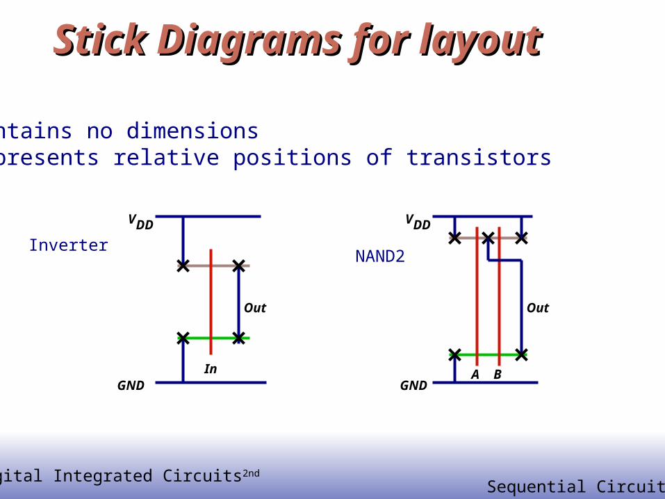
Stick Diagrams for layoutStick Diagrams for layout
Contains no dimensionsRepresents relative positions of transistors
In
Out
VDD
GND
Inverter
A
Out
VDD
GNDB
NAND2
© Digital Integrated Circuits2nd
Sequential Circuits
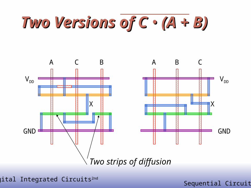
Two Versions of C Two Versions of C •• (A + B) (A + B)
X
CA B A B C
X
VDD
GND
VDD
GND
Two strips of diffusion
© Digital Integrated Circuits2nd
Sequential Circuits
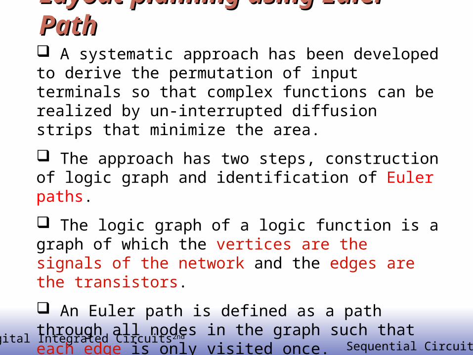
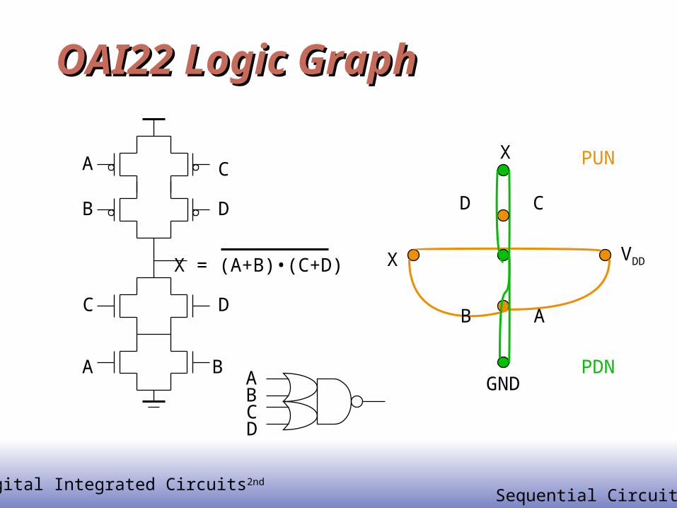
Layout planning using Euler PathLayout planning using Euler Path A systematic approach has been developed to derive the permutation of input terminals so that complex functions can be realized by un-interrupted diffusion strips that minimize the area.
The approach has two steps, construction of logic graph and identification of Euler paths.
The logic graph of a logic function is a graph of which the vertices are the signals of the network and the edges are the transistors.
An Euler path is defined as a path through all nodes in the graph such that each edge is only visited once.
The Euler paths for PDN and PUN must be the same in order to use a single poly for each input signal
© Digital Integrated Circuits2nd
Sequential Circuits
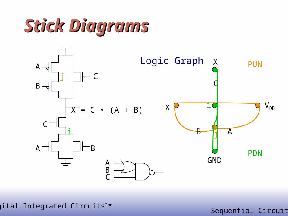
Stick DiagramsStick Diagrams
C
A B
X = C • (A + B)
B
AC
i
j
j
VDDX
X
i
GND
AB
C
PUN
PDNABC
Logic Graph
© Digital Integrated Circuits2nd
Sequential Circuits
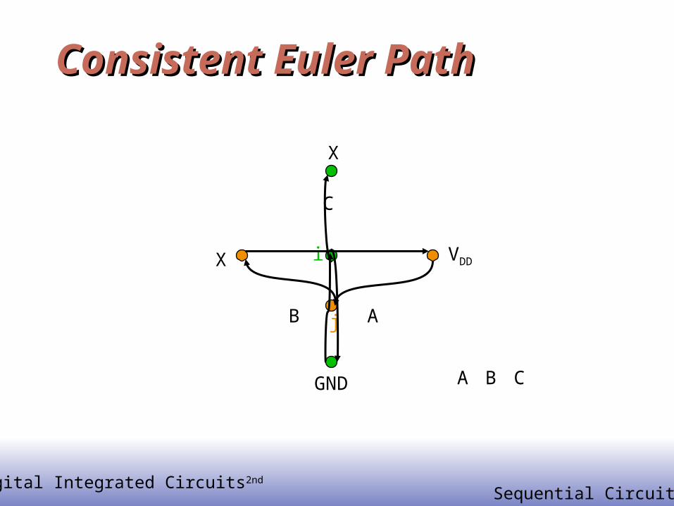
Consistent Euler PathConsistent Euler Path
j
VDDX
X
i
GND
AB
C
A B C
© Digital Integrated Circuits2nd
Sequential Circuits
OAI22 Logic GraphOAI22 Logic Graph
C
A B
X = (A+B)•(C+D)
B
A
D
VDDX
X
GND
AB
C
PUN
PDN
C
D
D
ABCD

© Digital Integrated Circuits2nd
Sequential Circuits
Example: x = ab+cdExample: x = ab+cd
GND
x
a
b c
d
VDDx
GND
x
a
b c
d
VDDx
(a) Logic graphs for (ab+cd) (b) Euler Paths {a b c d}
a c d
x
VDD
GND
(c) stick diagram for ordering {a b c d}
b
© Digital Integrated Circuits2nd
Sequential Circuits
NotesNotes The above layout technique is for single finger transistors.
When it comes to one strip of diffusion but with each transistor having multiple fingers, layout further complicate and you may still be able to do so.
© Digital Integrated Circuits2nd
Sequential Circuits
Digital Integrated Digital Integrated CircuitsCircuitsA Design PerspectiveA Design Perspective
Designing SequentialDesigning SequentialLogic CircuitsLogic Circuits
Jan M. RabaeyAnantha ChandrakasanBorivoje Nikolic
Revised from Digital Integrated Circuits, © Jan M. Rabaey el
© Digital Integrated Circuits2nd
Sequential Circuits
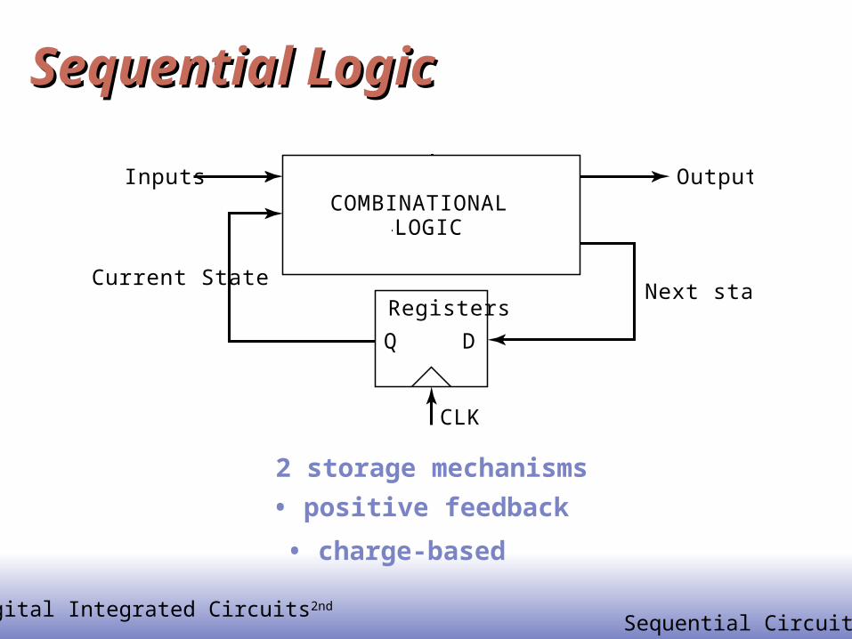
Sequential LogicSequential Logic
2 storage mechanisms
• positive feedback
• charge-based
COMBINATIONALLOGIC
Registers
Outputs
Next state
CLK
Q D
Current State
Inputs
© Digital Integrated Circuits2nd
Sequential Circuits
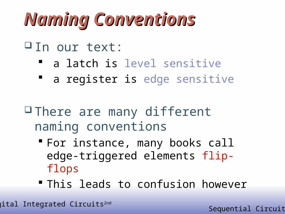
Naming ConventionsNaming Conventions In our text:
a latch is level sensitive a register is edge sensitive
There are many different naming conventions For instance, many books call edge-
triggered elements flip-flops This leads to confusion however
© Digital Integrated Circuits2nd
Sequential Circuits
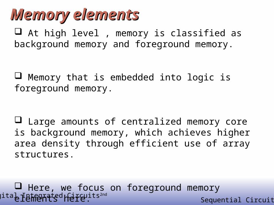
Memory elementsMemory elements At high level , memory is classified as background memory and foreground memory.
Memory that is embedded into logic is foreground memory.
Large amounts of centralized memory core is background memory, which achieves higher area density through efficient use of array structures.
Here, we focus on foreground memory elements here.

© Digital Integrated Circuits2nd
Sequential Circuits
Latch versus RegisterLatch versus Register Latch
stores data when clock is high or low
D
Clk
Q D
Clk
Q
Register
stores data when clock rises or falls
Clk Clk
D D
Q Q
© Digital Integrated Circuits2nd
Sequential Circuits
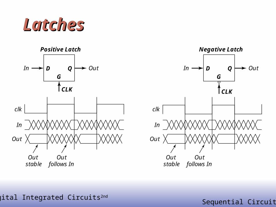
LatchesLatches
In
clk
In
Out
Positive Latch
CLK
DG
Q
Out
Outstable
Outfollows In
In
clk
In
Out
Negative Latch
CLK
DG
Q
Out
Outstable
Outfollows In
© Digital Integrated Circuits2nd
Sequential Circuits
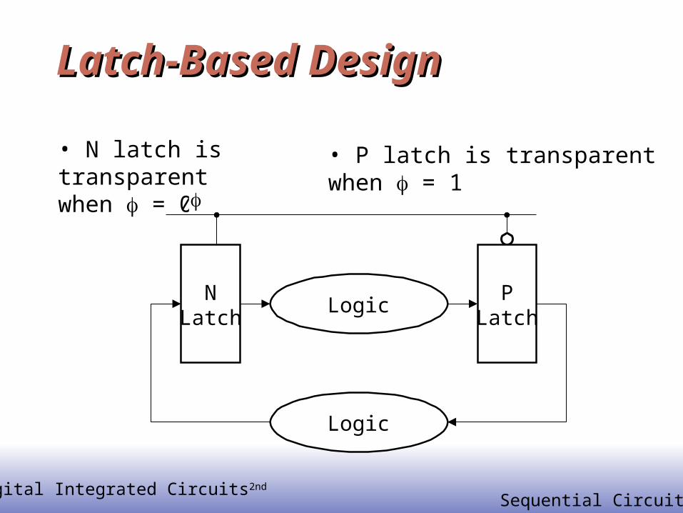
Latch-Based DesignLatch-Based Design
• N latch is transparentwhen = 0
• P latch is transparent when = 1
NLatch
Logic
Logic
PLatch
© Digital Integrated Circuits2nd
Sequential Circuits
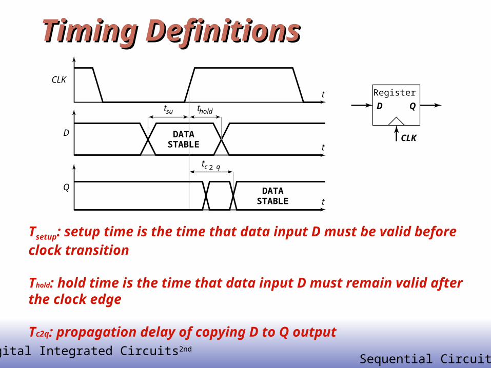
Timing DefinitionsTiming Definitions
t
CLK
t
D
tc2 q
tholdtsu
t
Q DATASTABLE
DATASTABLE
Register
CLK
D Q
Tsetup: setup time is the time that data input D must be valid before clock transition
Thold: hold time is the time that data input D must remain valid after the clock edge
Tc2q: propagation delay of copying D to Q output
© Digital Integrated Circuits2nd
Sequential Circuits
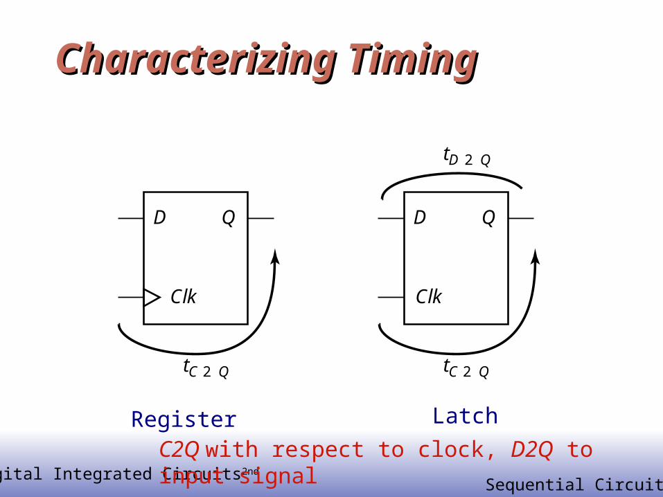
Characterizing TimingCharacterizing Timing
Clk
D Q
tC 2 Q
Clk
D Q
tC 2 Q
tD 2 Q
Register Latch
C2Q with respect to clock, D2Q to input signal

© Digital Integrated Circuits2nd
Sequential Circuits
Maximum Clock FrequencyMaximum Clock Frequency
FF
’s
LOGIC
tp,comb
Also another constraint: tcd,reg + tcd,logic > =thold
tcd: contamination delay = minimum delayThis constraint ensures the input data of the sequential circuits is held long enough after the clock edge and not modified too soon by the new coming-in data
tc2q + tp,comb + tsetup <= T
Clock period T must accommodate the longest possible delay
© Digital Integrated Circuits2nd
Sequential Circuits
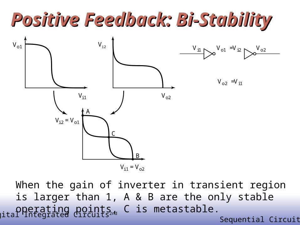
Positive Feedback: Bi-StabilityPositive Feedback: Bi-StabilityVi1 Vo2
Vo2 =Vi1
Vo1 =Vi2
Vi1
A
C
B
Vo2
Vi1=Vo2
Vo1 Vi2
Vi2=Vo1
When the gain of inverter in transient region is larger than 1, A & B are the only stable operating points, C is metastable.

© Digital Integrated Circuits2nd
Sequential Circuits
Meta-StabilityMeta-Stability
Gain should be larger than 1 in the transition region
A
C
d
B
Vi2
5V
o1
Vi1 5Vo2
A
C
d
B
Vi2
5V
o1
Vi1 5Vo2
Hence, cross coupling of two inverters results in a bistable circuit, that is a circuit with two stable states. The circuit serves as a memory, storing either a 1 or 0 (A or B)
© Digital Integrated Circuits2nd
Sequential Circuits
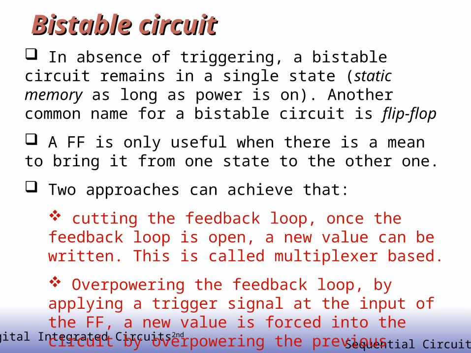
Bistable circuitBistable circuit In absence of triggering, a bistable circuit remains in a single state (static memory as long as power is on). Another common name for a bistable circuit is flip-flop
A FF is only useful when there is a mean to bring it from one state to the other one.
Two approaches can achieve that:
cutting the feedback loop, once the feedback loop is open, a new value can be written. This is called multiplexer based.
Overpowering the feedback loop, by applying a trigger signal at the input of the FF, a new value is forced into the circuit by overpowering the previous stored value.
© Digital Integrated Circuits2nd
Sequential Circuits
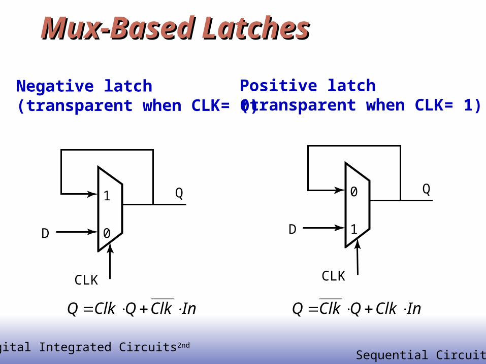
Mux-Based LatchesMux-Based Latches
Negative latch(transparent when CLK= 0)
Positive latch(transparent when CLK= 1)
CLK
1
0D
Q 0
CLK
1D
Q
InClkQClkQ InClkQClkQ
Related Documents