© 2016 IEEE. Personal use of this material is permitted. Permission from IEEE must be obtained for all other uses, in any current or future media, including reprinting/republishing this material for advertising or promotional purposes, creating new collective works, for resale or redistribution to servers or lists, or reuse of any copyrighted component of this work in other works. Digital Object Identifier (DOI): 10.1109/ECCE.2016.7854899 Energy Conversion Congress and Exposition Bidirectional Series-Resonant DC-DC Converter with Fault-Tolerance Capability for Smart Transformer Levy Ferreira Costa Giampaolo Buticchi Marco Liserre Suggested Citation L. F. Costa, G. Buticchi and M. Liserre, "Bidirectional Series-Resonant DC-DC Converter with Fault- Tolerance Capability for Smart Transformer," IEEE Energy Conversion Congress and Exposition (ECCE), Milwaukee, 2016.

Welcome message from author
This document is posted to help you gain knowledge. Please leave a comment to let me know what you think about it! Share it to your friends and learn new things together.
Transcript
© 2016 IEEE. Personal use of this material is permitted. Permission from IEEE must be obtained for
all other uses, in any current or future media, including reprinting/republishing this material for
advertising or promotional purposes, creating new collective works, for resale or redistribution to
servers or lists, or reuse of any copyrighted component of this work in other works.
Digital Object Identifier (DOI): 10.1109/ECCE.2016.7854899
Energy Conversion Congress and Exposition
Bidirectional Series-Resonant DC-DC Converter with Fault-Tolerance Capability for Smart
Transformer
Levy Ferreira Costa
Giampaolo Buticchi
Marco Liserre
Suggested Citation
L. F. Costa, G. Buticchi and M. Liserre, "Bidirectional Series-Resonant DC-DC Converter with Fault-
Tolerance Capability for Smart Transformer," IEEE Energy Conversion Congress and Exposition (ECCE),
Milwaukee, 2016.
Bidirectional Series-Resonant DC-DC Converter
with Fault-Tolerance Capability for Smart
Transformer
Levy Costa, Giampaolo Buticchi and Marco Liserre
Christian-Albrecht-University of Kiel (Uni-Kiel) / Power Electronics Chair (PE)
Kaiserstr. 2, 24143, Kiel, SH, Germany
Email: {lfc,gibu, ml}@tf.uni-kiel.de
Abstract—The Series-Resonant dc-dc converter (SRC) is widelyused in several application and it became very popular in SmartTransformer application. In this application, fault tolerance isa highly desired feature and it is obtained through redundancy.This paper proposes a reconfiguration scheme for the SRC forthe case of failure in one semiconductor, which could drasticallyreduce the need of redundancy. Using the proposed scheme,the full-bridge based SRC can be reconfigured in a half-bridgetopology, in order to keep the converter operational even withthe failure (open circuit or short circuit) of one switch. Thetheoretical analysis is carried out for the unidirectional SRCand then extended to the bidirectional topology, since bidirec-tionality is required in smart transformer application. To verifythe feasibility of the proposed scheme, the converter is testedexperimentally in a 700 V to 600 V prototype with 10 kW ofoutput power. A IGBT short-circuit fault is tested and the resultsconfirms the effectiveness of the proposed approach.
I. INTRODUCTION
The series-resonant dc-dc converter (SRC) has been very
used in wireless power transfer application for electrical ve-
hicle [1] - [4], battery charger [5] - [6], renewable energy
system [7]- [10] and high voltage power supply for specific
application, such as traveling-wave tube (TWT) for satellite
application [11]. Recently, this topology became very popular
in Smart Transformer (ST) [12]–[15], mainly because of its
characteristic of output voltage regulation in open loop asso-
ciate to its high efficiency. Fig. 1 shows a modular architecture
of the ST using the SRC as a building block of the dc-dc stage.
In ST applied in the smart grid context, the continuity
of operation is of paramount importance [12], [16]. For that
reason, a highly reliable system (preferable with redundancies)
is required. The fault tolerant feature contributes to increase
the availability of system and several fault tolerance methods
have been proposed in literature [17]–[20]. Most of these
methods includes a significant amount of extra hardware
(such as semiconductors/leg redundancy [17], [19] or series
connection of fuses/switches to isolate the fault [17], [18],
[20]), increasing the cost and compromising the efficiency
of the system. In this context, this paper proposes a fault
tolerance solution with minimum of additional hardware and
no impact on efficiency for the SRC converter, using the
advantage of inherent fault tolerant capability of this topology.
The investigated method have been introduced in [21] for
the unidirectional version. However, bidirectional feature is
Figure 1. Modular Smart Transformer architecture using the Series-Resonantconverter as a building block of the dc-dc stage of the system.
required for all converters in ST application and then, the fault
tolerance method is extended to the bidirectional SRC in this
work.
Independently from the mechanism, there are two possible
failures types for the semiconductor: open-circuit (OC) or
short-circuit (SC). According to [22], [23], the reasons that
implies a OC failure are: bond-wire lift off or rupture and
failure on the gate drive. Meanwhile, the SC failure might be
a result of an overvoltage, static or dynamic latch up, second
breakdown or energy shock. Since most of the failures result
in a SC condition [22], this work focuses on a SRC resilient
to SC failure.
The proposed reconfiguration scheme consists in re-
configuring the full-bridge SRC (FB-SRC) in a half-bridge
SRC (HB-SRC) converter. Nevertheless, the output voltage
generated by the HB-SRC is half of the output generated
by the FB-SRC, considering the same parameters. There-
fore, a novel re-configurable rectifier based on the voltage-
doubler topology is proposed in order to keep the same output
voltage. The operation principle of the FB-SRC and HB-
SRC operating in discontinuous conduction mode (dcm) are
presented in Section II. In Section III, the reconfiguration
scheme is described in detail for the unidirectional SRC and
the proposed fault-tolerant topology is presented. In section
IV, the proposed reconfiguration scheme is extended to the
bidirectional topology and a bidirectional fault-tolerant SRC
is proposed. Experimental results are provided in Section V,
in order to confirm the theoretical analysis developed in this
paper. Finally, the conclusion is presented in Section VI.
II. OPERATION PRINCIPLE OF THE SR CONVERTER
A. Full-Bridge SRC
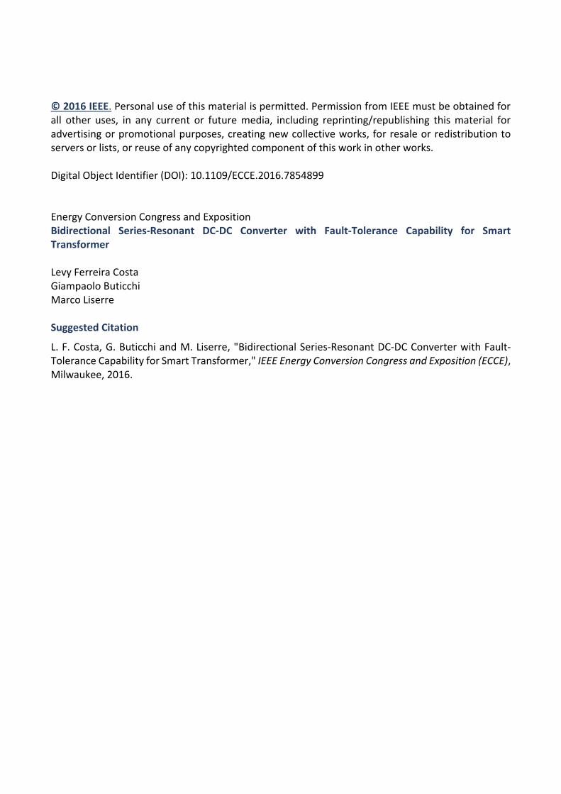
The topology of the SRC based on full-bridge configuration
(FB-SRC) is shown in Fig. 1 (a). To simplify the description,
a unidirectional topology is considered in this analysis and a
diode bridge rectifier is used in the secondary side. To support
the analysis, the variables resonant frequency ( fo), resonant
angular frequency (ω0) and characteristic impedance of the
resonant network (Z) are defined from (1) to (3), in terms
of the resonant inductor (Lr) and capacitor (Cr) of the tank
circuit.
f0 =1
2π√
LrCr
(1)
ω0 = 2π f0 (2)
Z =
√Lr
Cr
(3)
Fig. 1 (c) shows the main waveforms for the FB-SRC
operating at the resonant frequency ( fs = fo) and below
the resonant frequency ( fs < fo), where fs is the switching
frequency. For operation below the resonant frequency, the
current iLr reaches zero before half of the switching period, and
it remains zero until the primary bridge applies negative output
voltage, i.e. vp = −Vi. Since the commutations happen when
iLr = 0, all semiconductors switch at zero-current-switching
(ZCS), avoiding therefore switching losses. Because of the
soft-switching feature, this operation mode, named half-cycle
discontinuous-conduction mode (dcm), is very advantageous
and it will be considered for the analysis in this work. To
operate at half-cycle dcm, the converter parameters must
satisfy the following conditions [24]:
γ =ω0
2 fs
> π (4)
fs < f0 (5)
Io < 8 fsCrVo (6)
where, γ is the angular length of one half switching period
and Io is the load current. From these conditions is possible
to design Lr and Cr, considering the operation range of the
converter.
The relation between the amount of charge stored in the
capacitor (∆q) and its voltage (vCr) is given by (7). During
the period 0 < t < T0 (where T0 is the resonant period), the
capacitor voltage starts from −VCpk and reaches VCpk (see Fig.
2 (c)), thus ∆vCr = 2VCpk. Likewise, the charge that flows
Figure 2. Series Resonant dc-dc converter: (a) topology of the FB-SRC, (b)Topology of the HB-SRC, (c) main waveforms of the FB-SRC and (d) mainwaveforms of the HB-SRC.
through the capacitor during this period is defined as q, as
shown in Fig. 2 (c). This relation is described in (8).
∆q =C∆vCr (7)
q = 2 ·C ·VCpk (8)
The instantaneous average value of the input current (ii) is
calculated by (9). As highlighted in this equation, the integral
of the current during the time interval 0 to Ts/2 is the charge
accumulated in the capacitor (see Fig. 2 (c)). Thus, the relation
presented in (10) is found.
Ii = 〈i1(t)〉T s =2
Ts
Ts/2∫
0
i1(t)dt
︸ ︷︷ ︸
q
(9)
Ii = 2 fsq (10)
Replacing (10) in (8), (11) is obtained, and it can be
rearranged to obtain the peak voltage on the capacitor in
function of the load (represented in this equation by the input
current Ii), switching frequency and capacitance value, as
presented in (12).
Ii
2 fsq= 2 ·C ·VCpk (11)
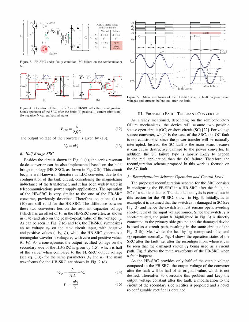
Figure 3. FB-SRC under faulty condition: SC failure on the semiconductors4.
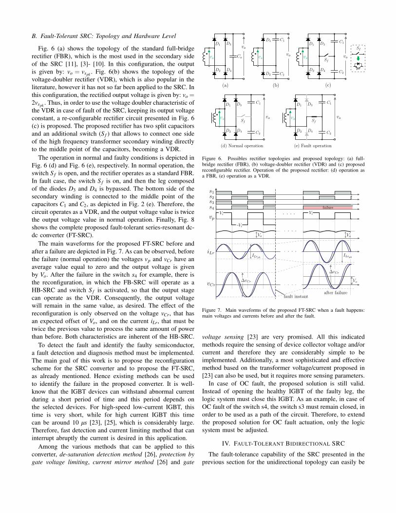
Figure 4. Operation of the FB-SRC as a HB-SRC after the reconfiguration.States operation of the SRC after the fault: (a) positive iL current (first state),(b) negative iL current(second state)
VCpk =Ii
8 fsC(12)
The output voltage of the converter is given by (13).
Vo = nVi (13)
B. Half-Bridge SRC
Besides the circuit shown in Fig. 1 (a), the series-resonant
dc-dc converter can be also implemented based on the half-
bridge topology (HB-SRC), as shown in Fig. 2 (b). This circuit
became well-known in literature as LLC converter, due to the
configuration of the tank circuit, considering the magnetizing
inductance of the transformer, and it has been widely used in
telecommunications power supply applications. The operation
of the HB-SRC is very similar to the one of the FB-SRC
converter, previously described. Therefore, equations (4) to
(10) are still valid for the HB-SRC. The difference between
these two converters lies on the resonant capacitor voltage
(which has an offset of Vo in the HB-SRC converter, as shown
in (14)) and also on the peak-to-peak value of the voltage vp.
As can be seen in Fig. 2 (c) and (d), the FB-SRC synthesizes
an ac voltage vp on the tank circuit input, with negative
and positive values (−Vi, Vi), while the HB-SRC generates a
rectangular waveform voltage vp with zero and positive values
(0, Vi). As a consequence, the output rectified voltage on the
secondary side of the HB-SRC is given by (15), which is half
of the value, when compared to the FB-SRC output voltage
(see eq. (13)) for the same parameters (Vi and n). The main
waveforms for the HB-SRC are shown in Fig. 2 (d).
VCp =Ii
8 fsC+Vo (14)
Vo =nVi
2(15)
Figure 5. Main waveforms of the FB-SRC when a fault happens: mainvoltages and currents before and after the fault.
III. PROPOSED FAULT TOLERANT CONVERTER
As already mentioned, depending on the semiconductors
failure mechanisms, the device will assume two possible
states: open-circuit (OC) or short-circuit (SC) [22]. For voltage
source converter, which is the case of the SRC, the OC fault
is not catastrophic, since the power transfer will be naturally
interrupted. Instead, the SC fault is the main issue, because
it can cause destructive damage to the power converter. In
addition, the SC failure type is mostly likely to happen
in the real application than the OC failure. Therefore, the
reconfiguration scheme proposed in this work is focused on
the SC fault.
A. Reconfiguration Scheme: Operation and Control Level
The proposed reconfiguration scheme for the SRC consists
in configuring the FB-SRC in a HB-SRC after the fault, i.e.
SC of a semiconductor. The detailed analysis is carried out in
this section for the FB-SRC shown in Fig. 3. Initially, as an
example, it is assumed that the switch s4 is damaged in SC (see
Fig. 3) and hence the switch s3 must remain open, avoiding
short-circuit of the input voltage source. Since the switch s4 is
short-circuited, the point b (highlighted in Fig. 3) is directly
connected to the primary side ground and the damaged device
is used as a circuit path, resulting in the same circuit of the
Fig. 2 (b). Meanwhile, the healthy leg (composed of s1 and
s2) operates normally. Fig. 4 shows the operation states of the
SRC after the fault, i.e. after the reconfiguration, where it can
be seen that the damaged switch s4 being used as a circuit
path. Fig. 5 shows the main waveforms of the FB-SRC when
a fault happens.
As the HB-SRC provides only half of the output voltage
compared to the FB-SRC, the output voltage of the converter
after the fault will be half of its original value, which is not
desired. Thereafter, to overcome this problem and keep the
output voltage constant after the fault, a modification to the
circuit of the secondary side rectifier is proposed and a novel
re-configurable rectifier is obtained.
B. Fault-Tolerant SRC: Topology and Hardware Level
Fig. 6 (a) shows the topology of the standard full-bridge
rectifier (FBR), which is the most used in the secondary side
of the SRC [11], [3]- [10]. In this configuration, the output
is given by: vo = vspk. Fig. 6(b) shows the topology of the
voltage-doubler rectifier (VDR), which is also popular in the
literature, however it has not so far been applied to the SRC. In
this configuration, the rectified output voltage is given by: vo =2vspk
. Thus, in order to use the voltage doubler characteristic of
the VDR in case of fault of the SRC, keeping its output voltage
constant, a re-configurable rectifier circuit presented in Fig. 6
(c) is proposed. The proposed rectifier has two split capacitors
and an additional switch (S f ) that allows to connect one side
of the high frequency transformer secondary winding directly
to the middle point of the capacitors, becoming a VDR.
The operation in normal and faulty conditions is depicted in
Fig. 6 (d) and Fig. 6 (e), respectively. In normal operation, the
switch S f is open, and the rectifier operates as a standard FBR.
In fault case, the switch S f is on, and then the leg composed
of the diodes D3 and D4 is bypassed. The bottom side of the
secondary winding is connected to the middle point of the
capacitors C1 and C2, as depicted in Fig. 2 (e). Therefore, the
circuit operates as a VDR, and the output voltage value is twice
the output voltage value in normal operation. Finally, Fig. 8
shows the complete proposed fault-tolerant series-resonant dc-
dc converter (FT-SRC).
The main waveforms for the proposed FT-SRC before and
after a failure are depicted in Fig. 7. As can be observed, before
the failure (normal operation) the voltages vp and vCr have an
average value equal to zero and the output voltage is given
by Vo. After the failure in the switch s4 for example, there is
the reconfiguration, in which the FB-SRC will operate as a
HB-SRC and switch S f is activated, so that the output stage
can operate as the VDR. Consequently, the output voltage
will remain in the same value, as desired. The effect of the
reconfiguration is only observed on the voltage vCr, that has
an expected offset of Vo, and on the current iLr, that must be
twice the previous value to process the same amount of power
than before. Both characteristics are inherent of the HB-SRC.
To detect the fault and identify the faulty semiconductor,
a fault detection and diagnosis method must be implemented.
The main goal of this work is to propose the reconfiguration
scheme for the SRC converter and to propose the FT-SRC,
as already mentioned. Hence existing methods can be used
to identify the failure in the proposed converter. It is well-
know that the IGBT devices can withstand abnormal current
during a short period of time and this period depends on
the selected devices. For high-speed low-current IGBT, this
time is very short, while for high current IGBT this time
can be around 10 µs [23], [25], which is considerably large.
Therefore, fast detection and current limiting method that can
interrupt abruptly the current is desired in this application.
Among the various methods that can be applied to this
converter, de-saturation detection method [26], protection by
gate voltage limiting, current mirror method [26] and gate
Figure 6. Possibles rectifier topologies and proposed topology: (a) full-bridge rectifier (FBR), (b) voltage-doubler rectifier (VDR) and (c) proposedreconfigurable rectifier. Operation of the proposed rectifier: (d) operation asa FBR, (e) operation as a VDR.
Figure 7. Main waveforms of the proposed FT-SRC when a fault happens:main voltages and currents before and after the fault.
voltage sensing [23] are very promised. All this indicated
methods require the sensing of device collector voltage and/or
current and therefore they are considerably simple to be
implemented. Additionally, a most sophisticated and effective
method based on the transformer voltage/current proposed in
[23] can also be used, but it requires more sensing parameters.
In case of OC fault, the proposed solution is still valid.
Instead of opening the healthy IGBT of the faulty leg, the
logic system must close this IGBT. As an example, in case of
OC fault of the switch s4, the switch s3 must remain closed, in
order to be used as a path of the circuit. Therefore, to extend
the proposed solution for OC fault actuation, only the logic
system must be adjusted.
IV. FAULT-TOLERANT BIDIRECTIONAL SRC
The fault-tolerance capability of the SRC presented in the
previous section for the unidirectional topology can easily be
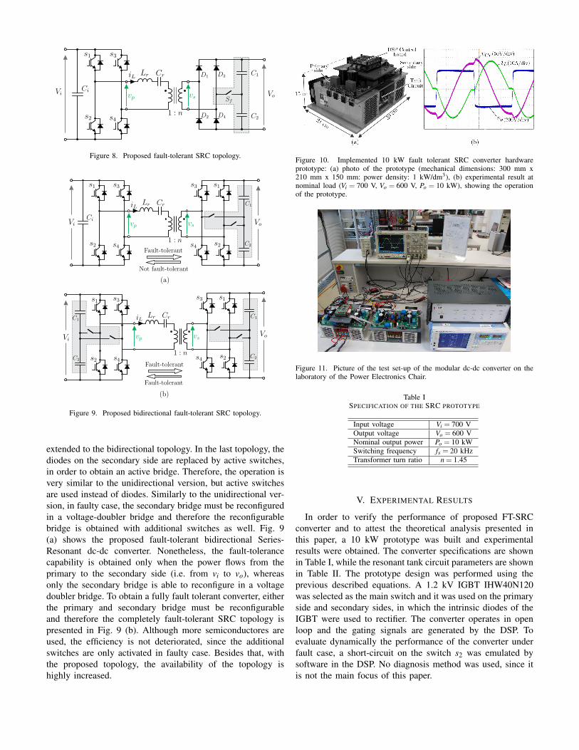
Figure 8. Proposed fault-tolerant SRC topology.
Figure 9. Proposed bidirectional fault-tolerant SRC topology.
extended to the bidirectional topology. In the last topology, the
diodes on the secondary side are replaced by active switches,
in order to obtain an active bridge. Therefore, the operation is
very similar to the unidirectional version, but active switches
are used instead of diodes. Similarly to the unidirectional ver-
sion, in faulty case, the secondary bridge must be reconfigured
in a voltage-doubler bridge and therefore the reconfigurable
bridge is obtained with additional switches as well. Fig. 9
(a) shows the proposed fault-tolerant bidirectional Series-
Resonant dc-dc converter. Nonetheless, the fault-tolerance
capability is obtained only when the power flows from the
primary to the secondary side (i.e. from vi to vo), whereas
only the secondary bridge is able to reconfigure in a voltage
doubler bridge. To obtain a fully fault tolerant converter, either
the primary and secondary bridge must be reconfigurable
and therefore the completely fault-tolerant SRC topology is
presented in Fig. 9 (b). Although more semiconductores are
used, the efficiency is not deteriorated, since the additional
switches are only activated in faulty case. Besides that, with
the proposed topology, the availability of the topology is
highly increased.
Figure 10. Implemented 10 kW fault tolerant SRC converter hardwareprototype: (a) photo of the prototype (mechanical dimensions: 300 mm x210 mm x 150 mm: power density: 1 kW/dm3), (b) experimental result atnominal load (Vi = 700 V, Vo = 600 V, Po = 10 kW), showing the operationof the prototype.
Figure 11. Picture of the test set-up of the modular dc-dc converter on thelaboratory of the Power Electronics Chair.
Table ISPECIFICATION OF THE SRC PROTOTYPE
Input voltage Vi = 700 V
Output voltage Vo = 600 V
Nominal output power Po = 10 kW
Switching frequency fs = 20 kHz
Transformer turn ratio n = 1.45
V. EXPERIMENTAL RESULTS
In order to verify the performance of proposed FT-SRC
converter and to attest the theoretical analysis presented in
this paper, a 10 kW prototype was built and experimental
results were obtained. The converter specifications are shown
in Table I, while the resonant tank circuit parameters are shown
in Table II. The prototype design was performed using the
previous described equations. A 1.2 kV IGBT IHW40N120
was selected as the main switch and it was used on the primary
side and secondary sides, in which the intrinsic diodes of the
IGBT were used to rectifier. The converter operates in open
loop and the gating signals are generated by the DSP. To
evaluate dynamically the performance of the converter under
fault case, a short-circuit on the switch s2 was emulated by
software in the DSP. No diagnosis method was used, since it
is not the main focus of this paper.
Figure 12. Experimental results of the FB-SRC (without the reconfigurable rectifier on the secondary side) under a fault on the switch s2: (a) dynamicbehavior of the converter during the fault, (b) steady-state operation before the fault and (c) steady-state operation after the fault. Experimental results of theproposed FT-SRC under a fault on the switch s2: (d) dynamic behavior of the converter during the fault, (e) steady-state operation before the fault and (f)steady-state operation after the fault.
Table IIMAIN PARAMETERS OF THE TANK CIRCUIT
Resonant capacitance Cr = 0.68µF
Resonant Inductor Lr = 79µH
Tank resonant angular frequency ω0 = 1.364 ·105 rad/s
Resonant frequency fo = 21.7 kHz
Angular length of half switching period γ = 0.577
Fig. 10 shows photo of the prototype and the main wave-
forms for the converter operating in steady-state at nominal
condition. The picture of the complete test set-up of the
modular prototype is depicted in Fig. 10, in which a modular
prototype composed by two dc-dc SRC is observed. The
results were obtained for the converter operating in steady-
state (before and after the fault) and also dynamically during
the fault and they are discussed herein. For safety reasons, the
dynamic results were obtained for reduced input and output
voltages.
Initially, the converter was tested considering only the
reconfiguration scheme in the primary bridge, without the
proposed re-configurable rectifier, in order to verify the inher-
ent capability to withstand a fault of the SRC. The test was
performed with input and output voltage of 200 V and 300
V, respectively, and the results for this condition are presented
in Fig. 12. The dynamic response of the FB-SRC during the
fault of the switch s2 is depicted in Fig. 12 (a), in which
is observed the converter remains operational after the fault,
proving its inherent ability to handle the fault, as described
in Section III.a. As expected the output voltage drops to half
of its value (from 300 V to 150 V) after the fault and the
capacitor voltage has an offset of Vo. The inductor current
is also reduced, because the test was performed with constant
resistance as load and therefore reduction on the output voltage
implies in reduction on power. The detailed waveforms before
and after the fault can observed in the Figs. 12 (b) and (c),
respectively.
Afterwards, the proposed unidirectional FT-SRC (including
the proposed rectifier) was tested, for an input voltage of 350 V
and output voltage of 500 V and the main results are presented
from Fig. 12 (c) to (f). The dynamic behavior during the fault
on switch s2 of the proposed FT-SRC is shown in Fig. 12
(c) and as can be seen in this figure, the converter remains
operational after the fault and it provides a constant output
voltage (500 V) even after the fault, attesting the effectiveness
of the proposed rectifier and the converter. As the output
voltage remains constant, the amount of processed power is
the same before and after the fault and therefore the amount of
current on the resonant tank is twice after the fault, because
of the HB configuration on the primary side. The detailed
waveforms before and after the fault can observed in the Figs.
12 (e) and (f), respectively. To summarize, the results have
shown that the proposed converter can handle a short-circuit
fault in one device and still provide the required output voltage
and power, keeping the continuity of operation.
VI. CONCLUSION
This paper has proposed a fault-tolerant series-resonant dc-
dc converter. The basic operation of the SRC based on the
full-bridge and half-bridge topologies was described. Then, a
semiconductor short-circuit fault case is evaluated for the full-
bridge series-resonant converter and a reconfiguration scheme,
in which the FB-SRC operates as a HB-SRC, is presented. As
a result of the reconfiguration, the output voltage is reduced.
To overcome this problem a modified rectifier that can be
reconfigured in a voltage doubler rectifier, keeping the output
voltage constant, is proposed.
The main advantages of the proposed converter are: post-
fault operation, simple implementation, reduced number of ad-
ditional component and no efficiency deterioration. However,
the resonant capacitor must be designed for higher voltage
and the current effort on the healthy devices in failure mode
operation is twice the than in normal mode operation.
Experimental results for a 10 kW prototype were obtained
and the effectiveness and advantages of the proposed fault
tolerant series resonant dc-dc converter has been demonstrated.
ACKNOWLEDGMENT
The research leading to these results has received funding
from the European Research Council under the European
Unions Seventh Framework Programme (FP/2007-2013) /
ERC Grant Agreement n. [616344] - Heart.
REFERENCES
[1] B. X. Nguyen, D. M. Vilathgamuwa, G. H. B. Foo, P. Wang, A. Ong,U. K. Madawala, and T. D. Nguyen, “An efficiency optimization schemefor bidirectional inductive power transfer systems,” IEEE Transactions
on Power Electronics, vol. 30, no. 11, pp. 6310–6319, Nov 2015.[2] A. Berger, M. Agostinelli, S. Vesti, J. A. Oliver, J. A. Cobos, and
M. Huemer, “A wireless charging system applying phase-shift andamplitude control to maximize efficiency and extractable power,” IEEE
Transactions on Power Electronics, vol. 30, no. 11, pp. 6338–6348, Nov2015.
[3] M. Petersen and F. Fuchs, “Load dependent power control in series-series compensated electric vehicle inductive power transfer systems,”in European Conference on Power Electronics and Applications (EPE-
ECCE Europe), Aug 2014, pp. 1–10.[4] N. Liu and T. G. Habetler, “Design of a universal inductive charger
for multiple electric vehicle models,” IEEE Transactions on Power
Electronics, vol. 30, no. 11, pp. 6378–6390, Nov 2015.[5] I. O. Lee, “Hybrid pwm-resonant converter for electric vehicle on-board
battery chargers,” IEEE Transactions on Power Electronics, vol. 31,no. 5, pp. 3639–3649, May 2016.
[6] N. Shafiei, M. Ordonez, M. Craciun, C. Botting, and M. Edington, “Burstmode elimination in high-power llc resonant battery charger for electricvehicles,” IEEE Transactions on Power Electronics, vol. 31, no. 2, pp.1173–1188, Feb 2016.
[7] D. Jovcic and B. Ooi, “High-power, resonant dc/dc converter forintegration of renewable sources,” in IEEE Bucharest PowerTech, June2009, pp. 1–6.
[8] D. Jovcic and L. Zhang, “Lcl dc/dc converter for dc grids,” IEEE
Transactions on Power Delivery, vol. 28, no. 4, pp. 2071–2079, Oct2013.
[9] X. Sun, Y. Shen, Y. Zhu, and X. Guo, “Interleaved boost-integrated llcresonant converter with fixed-frequency pwm control for renewable en-ergy generation applications,” IEEE Transactions on Power Electronics,vol. 30, no. 8, pp. 4312–4326, Aug 2015.
[10] C. Meyer and R. De Doncker, “Design of a three-phase series resonantconverter for offshore dc grids,” in 42nd IAS Annual Meeting. Confer-
ence Record of the 2007 IEEE Industry Applications Conference, Sept2007, pp. 216–223.
[11] T. Lazzarin, O. Custodio, C. Costa Motta, and I. Barbi, “An isolateddc-dc converter with high-output-voltage for a twta,” in International
Telecommunications Energy Conference (INTELEC), Sept 2014, pp. 1–7.
[12] M. Liserre, G. Buticchi, M. Andresen, G. D. Carne, L. F. Costa, andZ. X. Zou, “The smart transformer: Impact on the electric grid andtechnology challenges,” IEEE Industrial Electronics Magazine, vol. 10,no. 2, pp. 46–58, Summer 2016.
[13] D. Dujic, G. Steinke, E. Bianda, S. Lewdeni-Schmid, C. Zhao, andJ. Steinke, “Characterization of a 6.5kv igbt for medium-voltage high-power resonant dc-dc converter,” in Applied Power Electronics Confer-
ence and Exposition (APEC), March 2013, pp. 1438–1444.
[14] C. Zhao, D. Dujic, A. Mester, J. Steinke, M. Weiss, S. Lewdeni-Schmid, T. Chaudhuri, and P. Stefanutti, “Power electronic tractiontransformer:medium voltage prototype,” IEEE Transactions on Indus-
trial Electronics, vol. 61, no. 7, pp. 3257–3268, July 2014.
[15] D. Rothmund, J. Huber, and J. Kolar, “Operating behavior and design ofthe half-cycle discontinuous-conduction-mode series-resonant-converterwith small dc link capacitors,” in Workshop on Control and Modeling
for Power Electronics (COMPEL), June 2013, pp. 1–9.
[16] M. Liserre, M. Andresen, L. F. Costa, and G. Buticchi, “Power routingin modular smart transformers,” IEEE Industrial Electronics Magazine,2016 (in press).
[17] W. Zhang, D. Xu, P. N. Enjeti, H. Li, J. T. Hawke, and H. S. Krish-namoorthy, “Survey on fault-tolerant techniques for power electronicconverters,” IEEE Transactions on Power Electronics, vol. 29, no. 12,pp. 6319–6331, Dec 2014.
[18] Y. Song and B. Wang, “Survey on reliability of power electronicsystems,” IEEE Transactions on Power Electronics, vol. 28, no. 1, pp.591–604, Jan 2013.
[19] E. Ribeiro, A. Cardoso, and C. Boccaletti, “Fault-tolerant strategy for aphotovoltaic dc-dc converter,” IEEE Transactions on Power Electronics,vol. 28, no. 6, pp. 3008–3018, June 2013.
[20] X. Pei, S. Nie, Y. Chen, and Y. Kang, “Open-circuit fault diagnosisand fault-tolerant strategies for full-bridge dc-dc converters,” IEEE
Transactions on Power Electronics, vol. 27, no. 5, pp. 2550–2565, May2012.
[21] L. F. Costa, G. Buttichi, and M. Liserre, “Fault-tolerant series-resonantdc-dc converter,” IEEE Transactions on Power Electronics, 2016 (inpress).
[22] R. Wu, F. Blaabjerg, H. Wang, M. Liserre, and F. Iannuzzo, “Catas-trophic failure and fault-tolerant design of igbt power electronic con-verters - an overview,” in Conference of the IEEE Industrial Electronics
Society (IECON), Nov 2013, pp. 507–513.
[23] B. Lu and S. Sharma, “A literature review of igbt fault diagnostic andprotection methods for power inverters,” IEEE Transactions on Industry
Applications, vol. 45, no. 5, pp. 1770–1777, Sept 2009.
[24] K. Afridi, “Resonant and soft-switching techniques in power elec-tronics,” Department of Electrical, Computer and Energy, ColoradoUniversity, Colorado, USA, Lectures Note, 2014.
[25] I. T. AG, “Ikw40n120t2,” 2014. [Online].Available: www.infineon.com/dgdl/IKW40N120T2 2 4.pdf?fileId=db3a304412b407950112b426d87b3ad5
[26] F. Huang and F. Flett, “Igbt fault protection based on di/dt feedbackcontrol,” in Power Electronics Specialists Conference, June 2007, pp.
1478–1484.
Related Documents