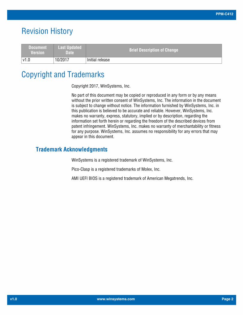
PPM-C412PC/104-Plus Single Board Computer
Based on DM&P Vortex DX3 CPU
Product Manual
WinSystems, Inc. | 715 Stadium Drive, Arlington, Texas 76011 | 817-274-7553 | [email protected] | www.winsystems.com
PPM-C412
v1.0
Revision History
Copyright and TrademarksCopyright 2017, WinSystems, Inc.
No part of this document may be copied or reproduced in any form or by any means without the prior written consent of WinSystems, Inc. The information in the document is subject to change without notice. The information furnished by WinSystems, Inc. in this publication is believed to be accurate and reliable. However, WinSystems, Inc. makes no warranty, express, statutory, implied or by description, regarding the information set forth herein or regarding the freedom of the described devices from patent infringement. WinSystems, Inc. makes no warranty of merchantability or fitness for any purpose. WinSystems, Inc. assumes no responsibility for any errors that may appear in this document.
Trademark Acknowledgments
WinSystems is a registered trademark of WinSystems, Inc.
Pico-Clasp is a registered trademarks of Molex, Inc.
AMI UEFI BIOS is a registered trademark of American Megatrends, Inc.
Document Version
Last Updated Date Brief Description of Change
v1.0 10/2017 Initial release
www.winsystems.com Page 2
PPM-C412
v1.0
Table of Contents
1 Before You Begin . . . . . . . . . . . . . . . . . . . . . . . . . . . . . . . . . . . . . . . . . 61.1 Warnings . . . . . . . . . . . . . . . . . . . . . . . . . . . . . . . . . . . . . . . . . . . . . . . . . . . . . . . . . . . . . . . . . . . . . . 6
2 Introduction. . . . . . . . . . . . . . . . . . . . . . . . . . . . . . . . . . . . . . . . . . . . . 6
3 Functionality . . . . . . . . . . . . . . . . . . . . . . . . . . . . . . . . . . . . . . . . . . . . 6
4 Features . . . . . . . . . . . . . . . . . . . . . . . . . . . . . . . . . . . . . . . . . . . . . . . 7
5 General Operation . . . . . . . . . . . . . . . . . . . . . . . . . . . . . . . . . . . . . . . . 95.1 System Block Diagram . . . . . . . . . . . . . . . . . . . . . . . . . . . . . . . . . . . . . . . . . . . . . . . . . . . . . . . . . . . . 9
6 Specifications . . . . . . . . . . . . . . . . . . . . . . . . . . . . . . . . . . . . . . . . . . 10
7 Configuration. . . . . . . . . . . . . . . . . . . . . . . . . . . . . . . . . . . . . . . . . . . 127.1 Component Layout . . . . . . . . . . . . . . . . . . . . . . . . . . . . . . . . . . . . . . . . . . . . . . . . . . . . . . . . . . . . . . 12
7.1.1 Top View. . . . . . . . . . . . . . . . . . . . . . . . . . . . . . . . . . . . . . . . . . . . . . . . . . . . . . . . . . . . . . 127.1.2 Bottom View . . . . . . . . . . . . . . . . . . . . . . . . . . . . . . . . . . . . . . . . . . . . . . . . . . . . . . . . . . . 147.1.3 Top View Indicators and Jumpers . . . . . . . . . . . . . . . . . . . . . . . . . . . . . . . . . . . . . . . . . . 15
7.2 I/O Port Map. . . . . . . . . . . . . . . . . . . . . . . . . . . . . . . . . . . . . . . . . . . . . . . . . . . . . . . . . . . . . . . . . . . 16
7.3 Interrupt Map . . . . . . . . . . . . . . . . . . . . . . . . . . . . . . . . . . . . . . . . . . . . . . . . . . . . . . . . . . . . . . . . . . 18
7.4 PCI Devices and Functions . . . . . . . . . . . . . . . . . . . . . . . . . . . . . . . . . . . . . . . . . . . . . . . . . . . . . . . . 19
7.5 DOS Legacy Memory Map . . . . . . . . . . . . . . . . . . . . . . . . . . . . . . . . . . . . . . . . . . . . . . . . . . . . . . . . 20
7.6 Memory Shadowing . . . . . . . . . . . . . . . . . . . . . . . . . . . . . . . . . . . . . . . . . . . . . . . . . . . . . . . . . . . . . 20
7.7 I/O Address Space . . . . . . . . . . . . . . . . . . . . . . . . . . . . . . . . . . . . . . . . . . . . . . . . . . . . . . . . . . . . . . 20
7.8 Digital I/O Register Definitions . . . . . . . . . . . . . . . . . . . . . . . . . . . . . . . . . . . . . . . . . . . . . . . . . . . . . 21
7.8.1 Port 0 through 5 I/O . . . . . . . . . . . . . . . . . . . . . . . . . . . . . . . . . . . . . . . . . . . . . . . . . . . . . 217.8.2 INT_PENDING. . . . . . . . . . . . . . . . . . . . . . . . . . . . . . . . . . . . . . . . . . . . . . . . . . . . . . . . . . 217.8.3 PAGE/LOCK . . . . . . . . . . . . . . . . . . . . . . . . . . . . . . . . . . . . . . . . . . . . . . . . . . . . . . . . . . . 217.8.4 POL0 through POL2 . . . . . . . . . . . . . . . . . . . . . . . . . . . . . . . . . . . . . . . . . . . . . . . . . . . . . 227.8.5 ENAB0 through ENAB2 . . . . . . . . . . . . . . . . . . . . . . . . . . . . . . . . . . . . . . . . . . . . . . . . . . . 227.8.6 INT_ID0 through INT_ID2. . . . . . . . . . . . . . . . . . . . . . . . . . . . . . . . . . . . . . . . . . . . . . . . . 22
7.9 Watchdog Timer. . . . . . . . . . . . . . . . . . . . . . . . . . . . . . . . . . . . . . . . . . . . . . . . . . . . . . . . . . . . . . . . 22
7.9.1 Advanced . . . . . . . . . . . . . . . . . . . . . . . . . . . . . . . . . . . . . . . . . . . . . . . . . . . . . . . . . . . . . 22
www.winsystems.com Page 3
PPM-C412
v1.0
7.9.2 Standard . . . . . . . . . . . . . . . . . . . . . . . . . . . . . . . . . . . . . . . . . . . . . . . . . . . . . . . . . . . . . . 237.9.3 Legacy . . . . . . . . . . . . . . . . . . . . . . . . . . . . . . . . . . . . . . . . . . . . . . . . . . . . . . . . . . . . . . . 23
7.10 Real-time Clock/Calendar . . . . . . . . . . . . . . . . . . . . . . . . . . . . . . . . . . . . . . . . . . . . . . . . . . . . . . . . . 24
7.11 SP1 Speaker. . . . . . . . . . . . . . . . . . . . . . . . . . . . . . . . . . . . . . . . . . . . . . . . . . . . . . . . . . . . . . . . . . . 24
7.12 Connectors . . . . . . . . . . . . . . . . . . . . . . . . . . . . . . . . . . . . . . . . . . . . . . . . . . . . . . . . . . . . . . . . . . . . 24
7.12.1 J1 SATA PWR SATA Power Connector . . . . . . . . . . . . . . . . . . . . . . . . . . . . . . . . . . . . . . . 247.12.2 J3 Power and Reset . . . . . . . . . . . . . . . . . . . . . . . . . . . . . . . . . . . . . . . . . . . . . . . . . . . . . 257.12.3 J4 External Battery Connector. . . . . . . . . . . . . . . . . . . . . . . . . . . . . . . . . . . . . . . . . . . . . . 257.12.4 J5/J6 PC104 PC/104 Bus . . . . . . . . . . . . . . . . . . . . . . . . . . . . . . . . . . . . . . . . . . . . . . . . . 267.12.5 J7 Multi I/O Connector . . . . . . . . . . . . . . . . . . . . . . . . . . . . . . . . . . . . . . . . . . . . . . . . . . . 287.12.6 J103 10/100/1000 Mbps Ethernet . . . . . . . . . . . . . . . . . . . . . . . . . . . . . . . . . . . . . . . . . . 337.12.7 J100 Gigabit Ethernet LEDs . . . . . . . . . . . . . . . . . . . . . . . . . . . . . . . . . . . . . . . . . . . . . . . 347.12.8 J8 CompactFlash Socket. . . . . . . . . . . . . . . . . . . . . . . . . . . . . . . . . . . . . . . . . . . . . . . . . . 357.12.9 J9 PC/104-Plus (PCI-104) Bus . . . . . . . . . . . . . . . . . . . . . . . . . . . . . . . . . . . . . . . . . . . . . 357.12.10 J101 SATA Serial ATA (SATA) . . . . . . . . . . . . . . . . . . . . . . . . . . . . . . . . . . . . . . . . . . . . . 377.12.11 J102 Digital Input/Output or GPIO . . . . . . . . . . . . . . . . . . . . . . . . . . . . . . . . . . . . . . . . . . 377.12.12 J104 LVDS/Audio Connector . . . . . . . . . . . . . . . . . . . . . . . . . . . . . . . . . . . . . . . . . . . . . . 387.12.13 J105 USB 2.0 Ports . . . . . . . . . . . . . . . . . . . . . . . . . . . . . . . . . . . . . . . . . . . . . . . . . . . . . 407.12.14 J106 Analog VGA Connector. . . . . . . . . . . . . . . . . . . . . . . . . . . . . . . . . . . . . . . . . . . . . . . 417.12.15 J107 Backlight Power Connector . . . . . . . . . . . . . . . . . . . . . . . . . . . . . . . . . . . . . . . . . . . 42
7.13 LED Indicators . . . . . . . . . . . . . . . . . . . . . . . . . . . . . . . . . . . . . . . . . . . . . . . . . . . . . . . . . . . . . . . . . 42
7.13.1 Vortex Fast Ethernet Indicators. . . . . . . . . . . . . . . . . . . . . . . . . . . . . . . . . . . . . . . . . . . . . 427.13.2 D6 Status LED . . . . . . . . . . . . . . . . . . . . . . . . . . . . . . . . . . . . . . . . . . . . . . . . . . . . . . . . . 437.13.3 i210T Gigabit Ethernet Indicator . . . . . . . . . . . . . . . . . . . . . . . . . . . . . . . . . . . . . . . . . . . . 43
8 BIOS. . . . . . . . . . . . . . . . . . . . . . . . . . . . . . . . . . . . . . . . . . . . . . . . . 438.1 General Information . . . . . . . . . . . . . . . . . . . . . . . . . . . . . . . . . . . . . . . . . . . . . . . . . . . . . . . . . . . . . 43
8.2 Entering Setup . . . . . . . . . . . . . . . . . . . . . . . . . . . . . . . . . . . . . . . . . . . . . . . . . . . . . . . . . . . . . . . . . 43
8.3 Navigating the Menus. . . . . . . . . . . . . . . . . . . . . . . . . . . . . . . . . . . . . . . . . . . . . . . . . . . . . . . . . . . . 43
8.4 BIOS Splash Screen . . . . . . . . . . . . . . . . . . . . . . . . . . . . . . . . . . . . . . . . . . . . . . . . . . . . . . . . . . . . . 43
8.5 BIOS Setting Storage Options . . . . . . . . . . . . . . . . . . . . . . . . . . . . . . . . . . . . . . . . . . . . . . . . . . . . . 53
8.5.1 CMOS Storage Locations . . . . . . . . . . . . . . . . . . . . . . . . . . . . . . . . . . . . . . . . . . . . . . . . . 538.5.2 Saving the CMOS Configuration . . . . . . . . . . . . . . . . . . . . . . . . . . . . . . . . . . . . . . . . . . . . 538.5.3 Updating the BIOS FLASH PROM . . . . . . . . . . . . . . . . . . . . . . . . . . . . . . . . . . . . . . . . . . . 53
9 Cables and Accessories . . . . . . . . . . . . . . . . . . . . . . . . . . . . . . . . . . . 53
www.winsystems.com Page 4
PPM-C412
v1.0
10 Software Drivers . . . . . . . . . . . . . . . . . . . . . . . . . . . . . . . . . . . . . . . . 54
A Best Practices . . . . . . . . . . . . . . . . . . . . . . . . . . . . . . . . . . . . . . . . . . 55
B Mechanical Drawings . . . . . . . . . . . . . . . . . . . . . . . . . . . . . . . . . . . . 58
C Power-on Self-Test (POST) Codes . . . . . . . . . . . . . . . . . . . . . . . . . . . . 60
D Warranty Information . . . . . . . . . . . . . . . . . . . . . . . . . . . . . . . . . . . . . 63
www.winsystems.com Page 5
PPM-C412/Before You Begin
v1.0
1. Before You BeginReview the warnings in this section and the best practice recommendations (see “Best Practices” on page 55) when using and handling the WinSystems PPM-C412. Following these recommendations provides an optimal user experience and prevents damage. Read through this document and become familiar with the PPM-C412 before proceeding.
1.1 Warnings
Only qualified personnel should configure and install the PPM-C412. While observing the best practices, pay particular attention to the following waning.
2. IntroductionThis manual provides configuration and usage information for the PPM-C412. If you still have questions, contact Technical Support at (817) 274-7553, Monday through Friday, between 8 AM and 5 PM Central Standard Time (CST).
Refer to the WinSystems website for other accessories (including cable drawings and pinouts) that can be used with your PPM-C412.
3. FunctionalityThe PPM-C412 is a single-board computer (SBC). It is a full-featured embedded system with a variety of on-board I/O options.
Two display interfaces (VGA and LVDS) are supported, along with stereo audio. Communication interfaces include one Fast Ethernet port, one Gigabit Ethernet port, four USB 2.0 ports, and four serial channels (two RS-232/422/485 and two RS-232). Twenty-four general-purpose I/O lines are individually programmable for input, output, or interrupt-driven applications, capable of fully latched event sensing with software-programmable polarity. For additional flexibility, the I/O lines can be paired with external isolation and relay modules.
FAILING TO COMPLY WITH THESE BEST PRACTICES MAY DAMAGE THE PPM-C412 AND VOID YOUR WARRANTY.
Avoid Electrostatic Discharge (ESD)Only handle the circuit board and other bare electronics when electrostatic discharge (ESD) protection is in place. Having a wrist strap and a fully grounded workstation is the minimum ESD protection required before the ESD seal on the product bag is broken.
www.winsystems.com Page 6
PPM-C412/Features
v1.0
The PPM-C412 provides an upgrade for existing PC/104-Plus compatible single board computers. Its designed for harsh environments and reliability, with an optional thermal solution for operating temperatures between -40 and +85°C (-40 and +185°F).
Linux and other x86 operating systems can be initialized from the SATA, CompactFlash, or USB interfaces. This provides flexible data storage options.
The PPM-C412 has an integrated display controller that interfaces to both VGA and LVDS panel displays. The video output mode is selected in the CMOS setup.
Simultaneous LVDS panel and VGA mode is also supported. The VGA connector is located at J106. The LVDS interface is located at J104. The mode is selected in the BIOS. The backlight power connector is located at J107.
Contact a WinSystems Applications Engineer for information about available cable kits and supported panels.
NOTE WinSystems can provide custom configurations for OEM clients. Please contact an Application Engineer for details.
4. FeaturesThe PPM-C412 provides the following features.
Processor
• DM&P 1 GHz Vortex DX3 SOC
Operating Systems (compatibility)
• Windows Embedded 7 (WES7)
• Linux
• DOS
• Other x86 RTOS
Memory
• Up to 2 GB of DDR3 SDRAM (soldered down)
BIOS
• AMI
Video
• VGA or LVDS (simultaneous operation supported)
• VGA resolutions up to 1920x1440
• LVDS resolutions up to 1600x1200 with 18-bits/pixel color panel support
www.winsystems.com Page 7
PPM-C412/Features
v1.0
Ethernet
• Intel® i210 10/100/1000 Mbps controller
• Vortex 10/100 Mbps controller
Storage
• 1 CompactFlash socket
• 1 SATA channel
General Purpose Input/Output (GPIO)
• 24 bidirectional 5V I/O lines capable of event sense and interrupt generation
Serial Interfaces
• Four USB 2.0 ports with ESD suppression
• Four serial COM ports
– Two RS232/422/485
– Two RS232 only
Bus Expansion
• PC/104-Plus (PC/104 and PCI-104)
Line Printer Port
• Bidirectional (SPP/ECP/EPP)
Watchdog Timer
• Up to 255 minute reset
Audio
• 2-channel line-level input
• 2-channel speaker-level output
• Stereo microphone input
Power
• +5V DC required, 1.2A typical
Industrial Operating Temperature
• -40 to +85°C (-40 to +185°F)
Form Factor
• 3.60” x 3.80” (90 mm x 96 mm)
Additional Features
• Real-time clock with optional battery backup
www.winsystems.com Page 8
PPM-C412/General Operation
v1.0
• Activity status LEDs on-board
• PS/2 keyboard and mouse supported
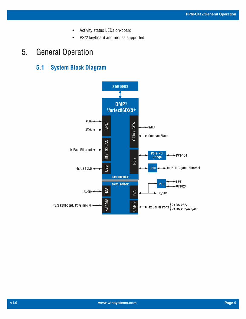
5. General Operation
5.1 System Block Diagram
www.winsystems.com Page 9
PPM-C412/Specifications
v1.0
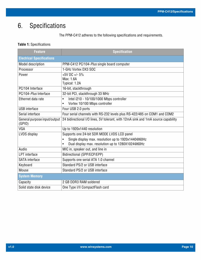
6. SpecificationsThe PPM-C412 adheres to the following specifications and requirements.
Table 1: Specifications
Feature Specification
Electrical Specifications
Model description PPM-C412 PC/104-Plus single board computerProcessor 1-GHz Vortex DX3 SOCPower +5V DC +/- 5%
Max: 1.6ATypical: 1.2A
PC/104 Interface 16-bit, stackthrough PC/104-Plus Interface 32-bit PCI, stackthrough 33 MHzEthernet data rate • Intel i210 - 10/100/1000 Mbps controller
• Vortex 10/100 Mbps controllerUSB interface Four USB 2.0 portsSerial interface Four serial channels with RS-232 levels plus RS-422/485 on COM1 and COM2General purpose input/output (GPIO)
24 bidirectional I/O lines, 5V tolerant, with 12mA sink and 1mA source capability
VGA Up to 1920x1440 resolutionLVDS display Supports one 24-bit SDR MODE LVDS LCD panel
• Single display max. resolution up to 1920x1440@60Hz• Dual display max. resolution up to 1280X1024@60Hz
Audio MIC in, speaker out, and line inLPT interface Bidirectional (SPP/ECP/EPP)SATA interface Supports one serial ATA 1.0 channelKeyboard Standard PS/2 or USB interfaceMouse Standard PS/2 or USB interface
System Memory
Capacity 2 GB DDR3 RAM solderedSolid state disk device One Type I/II CompactFlash card
www.winsystems.com Page 10
PPM-C412/Specifications
v1.0
Mechanical Specifications
Dimensions 3.6 x 3.8 inches (90 x 96 mm)Weight 5.8 oz (163 gm) with heat spreader / 8.98 oz (255 gm) with heatsinkBoard thickness 0.078 inches
Environmental Specifications
Temperature Operational from -40 to +65°C (-40 to +149°F) with heat spreader (still air)Operational from -40 to +85°C (-40 to +185°F) with heat spreader (300 LFM airflow)Operational from -40 to +80°C (-40 to +176°F) with additional heat sink (still air)Operational from -40 to +85°C (-40 to +185°F) with additional heat sink (200 LFM airflow)
Humidity (RH) 5% to 95% non-condensingMechanical shock testing MIL-STD-202G, Method 213B, Condition A 50g half-sine, 11 ms duration per axis, 3
axisRandom vibration testing MIL-STD-202G, Method 214A, Condition D .1g/Hz (11.95g rms), 20 minutes per
axis, 3 axisRoHS compliant YesMTBF 7.60 years, MIL-217 part count reliability method using manufacturer’s failure rate
data
Operating Systems
Runs Linux, DOS, Windows Embedded 7, and other x86-compatible operating systems
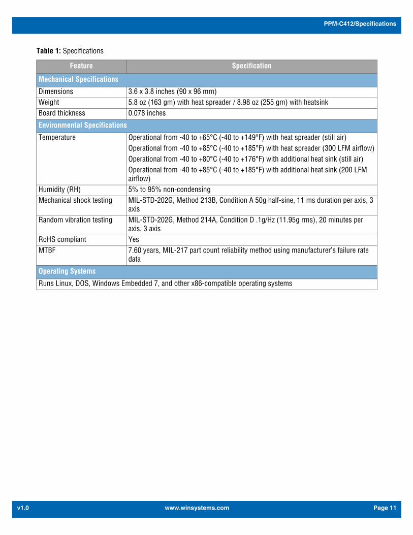
Table 1: Specifications
Feature Specification
www.winsystems.com Page 11
PPM-C412/Configuration
v1.0
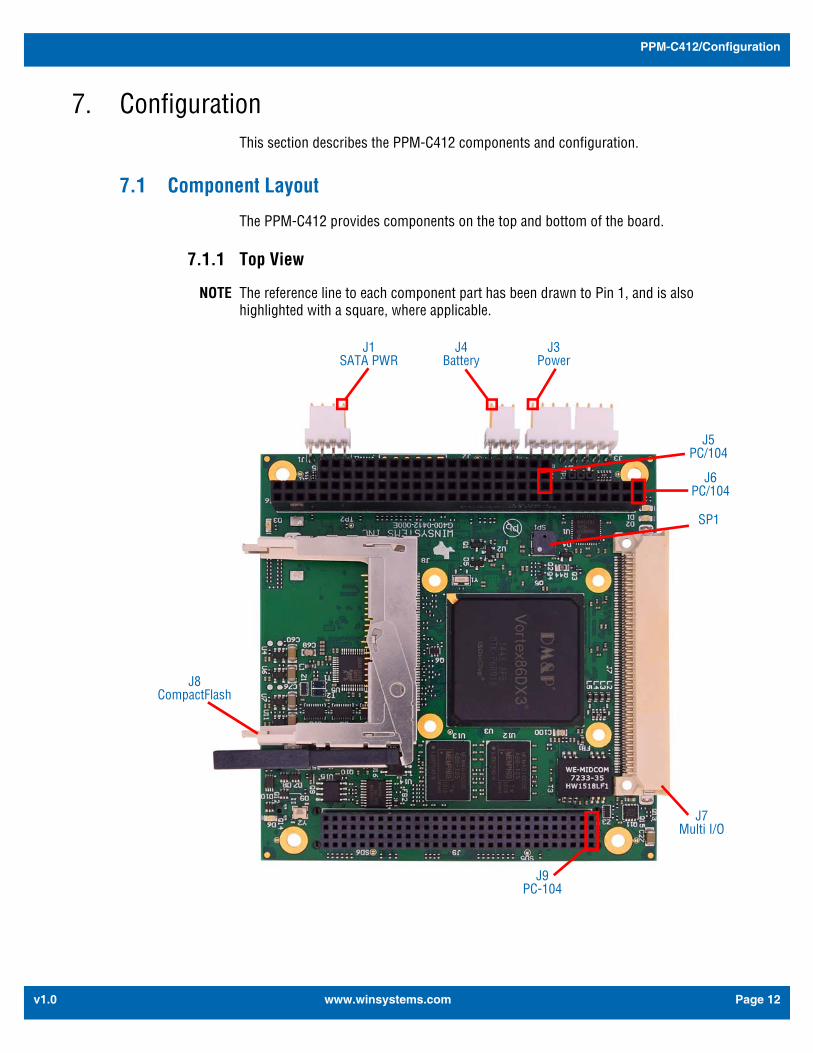
7. ConfigurationThis section describes the PPM-C412 components and configuration.
7.1 Component Layout
The PPM-C412 provides components on the top and bottom of the board.
7.1.1 Top View
NOTE The reference line to each component part has been drawn to Pin 1, and is also highlighted with a square, where applicable.
J4Battery
J7Multi I/O
J8CompactFlash
J1SATA PWR
J6PC/104
J9PC-104
J3Power
J5PC/104
SP1
www.winsystems.com Page 12
PPM-C412/Configuration
v1.0
Table 2: Top view components
Component Description Reference
J1 SATA power page 24J3 Power page 25J4 Battery page 25J5 PC/104 16 bit page 26J6 PC/104 8 bit page 26J7 Multi-I/O - PS/2 keyboard, PS/2 mouse, serial ports, 10/
100 ENET port, and LPTpage 28
J8 CompactFlash page 35J9 PCI-104 page 35
www.winsystems.com Page 13
PPM-C412/Configuration
v1.0
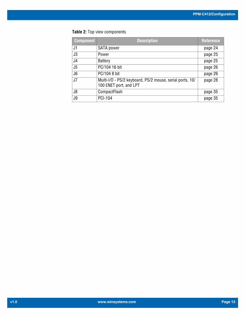
7.1.2 Bottom View
NOTE The reference line to each component part has been drawn to Pin 1, and is also highlighted with a square, where applicable.
J107LCD backlight
J101SATA
J106VGA
J105USB
J102GPIO
J104LVDS/audio
J100Gigabit Ethernet
LEDs
J103Gigabit
Ethernet
D100Gigabit
Ethernet LED
Table 3: Bottom view components
Component Description Reference
J100 Gigabit Ethernet LEDs page 34J101 SATA page 37J102 GPIO page 37J103 Gigabit Ethernet page 33J104 LVDS/audio page 38J105 4x USB 2.0 page 40J106 VGA page 41J107 LCD backlight page 42D100 Gigabit Ethernet activity (green) page 43
www.winsystems.com Page 14
PPM-C412/Configuration
v1.0
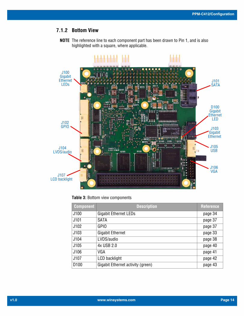
7.1.3 Top View Indicators and Jumpers
NOTE When installed in either position, the JP1 jumper causes a 6S boot delay. This must be installed to ensure proper boot when no external CMOS battery is connected.
D1 10/100 Ethernet speed
D2 10/100 Ethernet
link/activity
D3CFlashactivity
JP1battery
D6Status LED
Table 4: Top view LEDs
Component Description Color
D1 10/100 Ethernet speed Indicator RedD2 10/100 Ethernet link/activity indicator YellowD3 CFLASH activity RedD6 Status LED Green
Table 5: Jumper
Component Description
JP1 CMOS battery boot delay
www.winsystems.com Page 15
PPM-C412/Configuration
v1.0
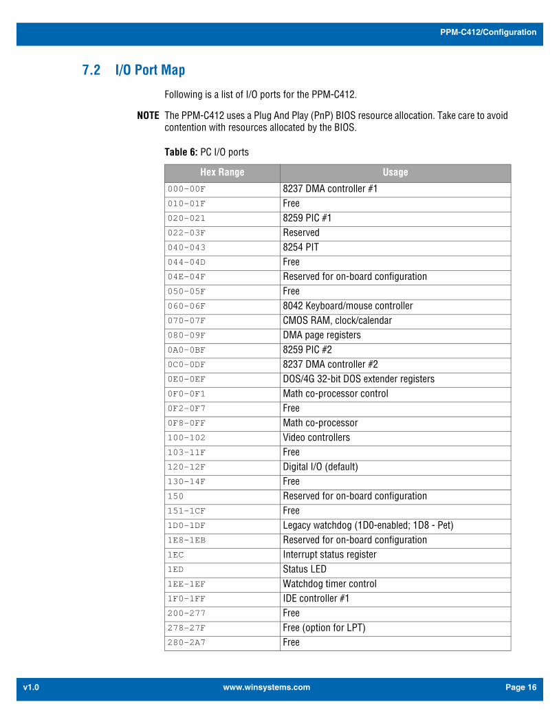
7.2 I/O Port Map
Following is a list of I/O ports for the PPM-C412.
NOTE The PPM-C412 uses a Plug And Play (PnP) BIOS resource allocation. Take care to avoid contention with resources allocated by the BIOS.
Table 6: PC I/O ports
Hex Range Usage
000-00F 8237 DMA controller #1010-01F Free020-021 8259 PIC #1022-03F Reserved040-043 8254 PIT044-04D Free04E-04F Reserved for on-board configuration050-05F Free060-06F 8042 Keyboard/mouse controller070-07F CMOS RAM, clock/calendar080-09F DMA page registers 0A0-0BF 8259 PIC #20C0-0DF 8237 DMA controller #20E0-0EF DOS/4G 32-bit DOS extender registers0F0-0F1 Math co-processor control0F2-0F7 Free0F8-0FF Math co-processor100-102 Video controllers103-11F Free120-12F Digital I/O (default)130-14F Free150 Reserved for on-board configuration151-1CF Free1D0-1DF Legacy watchdog (1D0-enabled; 1D8 - Pet)1E8-1EB Reserved for on-board configuration1EC Interrupt status register1ED Status LED1EE-1EF Watchdog timer control 1F0-1FF IDE controller #1200-277 Free278-27F Free (option for LPT)280-2A7 Free
www.winsystems.com Page 16
PPM-C412/Configuration
v1.0
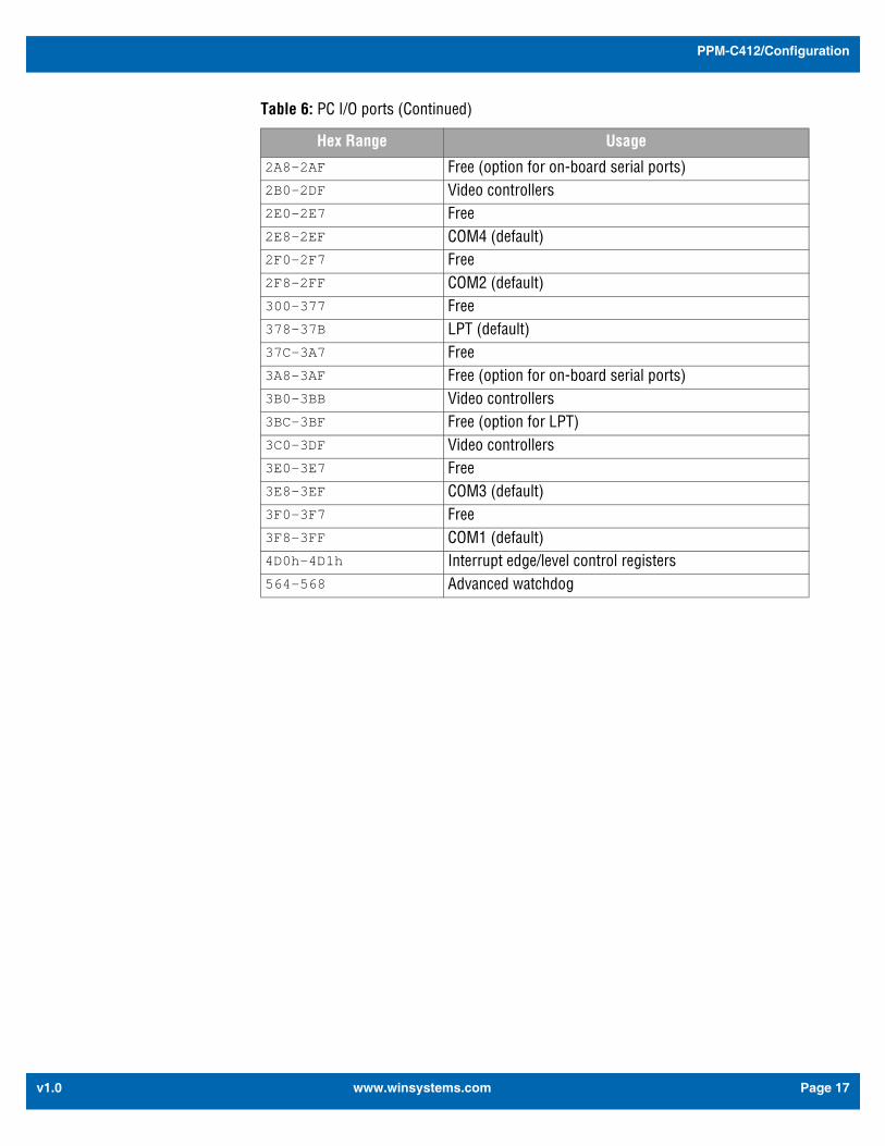
2A8-2AF Free (option for on-board serial ports) 2B0-2DF Video controllers2E0-2E7 Free2E8-2EF COM4 (default)2F0-2F7 Free2F8-2FF COM2 (default)300-377 Free378-37B LPT (default)37C-3A7 Free3A8-3AF Free (option for on-board serial ports)3B0-3BB Video controllers3BC-3BF Free (option for LPT) 3C0-3DF Video controllers3E0-3E7 Free3E8-3EF COM3 (default)3F0-3F7 Free3F8-3FF COM1 (default)4D0h-4D1h Interrupt edge/level control registers564-568 Advanced watchdog
Table 6: PC I/O ports (Continued)
Hex Range Usage
www.winsystems.com Page 17
PPM-C412/Configuration
v1.0
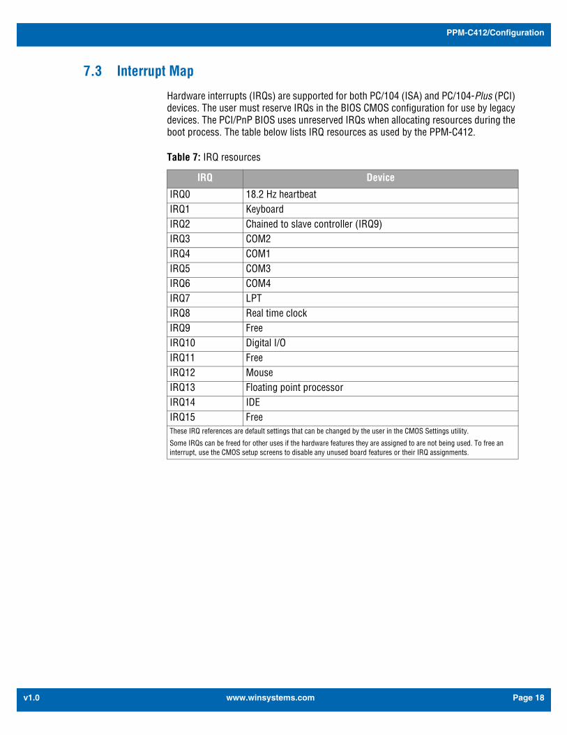
7.3 Interrupt Map
Hardware interrupts (IRQs) are supported for both PC/104 (ISA) and PC/104-Plus (PCI) devices. The user must reserve IRQs in the BIOS CMOS configuration for use by legacy devices. The PCI/PnP BIOS uses unreserved IRQs when allocating resources during the boot process. The table below lists IRQ resources as used by the PPM-C412.
Table 7: IRQ resources
IRQ Device
IRQ0 18.2 Hz heartbeat IRQ1 KeyboardIRQ2 Chained to slave controller (IRQ9) IRQ3 COM2IRQ4 COM1IRQ5 COM3IRQ6 COM4IRQ7 LPTIRQ8 Real time clockIRQ9 FreeIRQ10 Digital I/OIRQ11 FreeIRQ12 MouseIRQ13 Floating point processor IRQ14 IDEIRQ15 FreeThese IRQ references are default settings that can be changed by the user in the CMOS Settings utility.
Some IRQs can be freed for other uses if the hardware features they are assigned to are not being used. To free an interrupt, use the CMOS setup screens to disable any unused board features or their IRQ assignments.
www.winsystems.com Page 18
PPM-C412/Configuration
v1.0
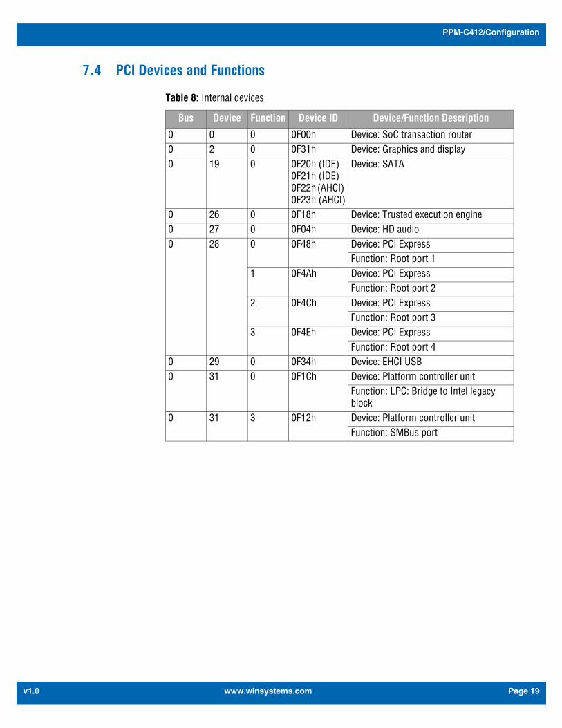
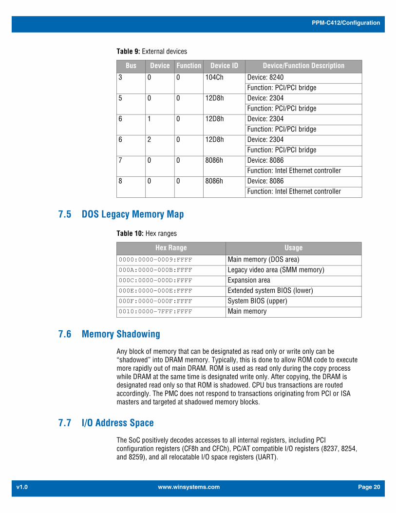
7.4 PCI Devices and Functions
Table 8: Internal devices
Bus Device Function Device ID Device/Function Description
0 0 0 0F00h Device: SoC transaction router0 2 0 0F31h Device: Graphics and display0 19 0 0F20h (IDE)
0F21h (IDE)0F22h (AHCI) 0F23h (AHCI)
Device: SATA
0 26 0 0F18h Device: Trusted execution engine0 27 0 0F04h Device: HD audio0 28 0 0F48h Device: PCI Express
Function: Root port 11 0F4Ah Device: PCI Express
Function: Root port 22 0F4Ch Device: PCI Express
Function: Root port 33 0F4Eh Device: PCI Express
Function: Root port 40 29 0 0F34h Device: EHCI USB0 31 0 0F1Ch Device: Platform controller unit
Function: LPC: Bridge to Intel legacy block
0 31 3 0F12h Device: Platform controller unitFunction: SMBus port
www.winsystems.com Page 19
PPM-C412/Configuration
v1.0
7.5 DOS Legacy Memory Map
7.6 Memory Shadowing
Any block of memory that can be designated as read only or write only can be “shadowed” into DRAM memory. Typically, this is done to allow ROM code to execute more rapidly out of main DRAM. ROM is used as read only during the copy process while DRAM at the same time is designated write only. After copying, the DRAM is designated read only so that ROM is shadowed. CPU bus transactions are routed accordingly. The PMC does not respond to transactions originating from PCI or ISA masters and targeted at shadowed memory blocks.
7.7 I/O Address Space
The SoC positively decodes accesses to all internal registers, including PCI configuration registers (CF8h and CFCh), PC/AT compatible I/O registers (8237, 8254, and 8259), and all relocatable I/O space registers (UART).
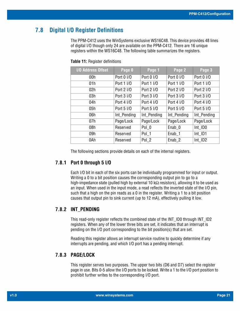
Table 9: External devices
Bus Device Function Device ID Device/Function Description
3 0 0 104Ch Device: 8240Function: PCI/PCI bridge
5 0 0 12D8h Device: 2304Function: PCI/PCI bridge
6 1 0 12D8h Device: 2304Function: PCI/PCI bridge
6 2 0 12D8h Device: 2304Function: PCI/PCI bridge
7 0 0 8086h Device: 8086Function: Intel Ethernet controller
8 0 0 8086h Device: 8086Function: Intel Ethernet controller
Table 10: Hex ranges
Hex Range Usage
0000:0000-0009:FFFF Main memory (DOS area)000A:0000-000B:FFFF Legacy video area (SMM memory)000C:0000-000D:FFFF Expansion area000E:0000-000E:FFFF Extended system BIOS (lower)000F:0000-000F:FFFF System BIOS (upper)0010:0000-7FFF:FFFF Main memory
www.winsystems.com Page 20
PPM-C412/Configuration
v1.0
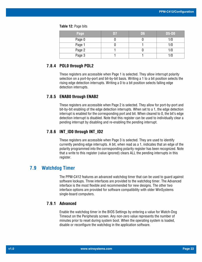
7.8 Digital I/O Register Definitions
The PPM-C412 uses the WinSystems exclusive WS16C48. This device provides 48 lines of digital I/O though only 24 are available on the PPM-C412. There are 16 unique registers within the WS16C48. The following table summarizes the registers.
The following sections provide details on each of the internal registers.
7.8.1 Port 0 through 5 I/O
Each I/O bit in each of the six ports can be individually programmed for input or output. Writing a 0 to a bit position causes the corresponding output pin to go to a high-impedance state (pulled high by external 10 kΩ resistors), allowing it to be used as an input. When used in the input mode, a read reflects the inverted state of the I/O pin, such that a high on the pin reads as a 0 in the register. Writing a 1 to a bit position causes that output pin to sink current (up to 12 mA), effectively pulling it low.
7.8.2 INT_PENDING
This read-only register reflects the combined state of the INT_ID0 through INT_ID2 registers. When any of the lower three bits are set, it indicates that an interrupt is pending on the I/O port corresponding to the bit position(s) that are set.
Reading this register allows an interrupt service routine to quickly determine if any interrupts are pending, and which I/O port has a pending interrupt.
7.8.3 PAGE/LOCK
This register serves two purposes. The upper two bits (D6 and D7) select the register page in use. Bits 0-5 allow the I/O ports to be locked. Write a 1 to the I/O port position to prohibit further writes to the corresponding I/O port.
Table 11: Register definitions
I/O Address Offset Page 0 Page 1 Page 2 Page 3
00h Port 0 I/O Port 0 I/O Port 0 I/O Port 0 I/O01h Port 1 I/O Port 1 I/O Port 1 I/O Port 1 I/O02h Port 2 I/O Port 2 I/O Port 2 I/O Port 2 I/O03h Port 3 I/O Port 3 I/O Port 3 I/O Port 3 I/O04h Port 4 I/O Port 4 I/O Port 4 I/O Port 4 I/O05h Port 5 I/O Port 5 I/O Port 5 I/O Port 5 I/O06h Int_Pending Int_Pending Int_Pending Int_Pending07h Page/Lock Page/Lock Page/Lock Page/Lock08h Reserved Pol_0 Enab_0 Int_ID009h Reserved Pol_1 Enab_1 Int_ID10Ah Reserved Pol_2 Enab_2 Int_ID2
www.winsystems.com Page 21
PPM-C412/Configuration
v1.0
7.8.4 POL0 through POL2
These registers are accessible when Page 1 is selected. They allow interrupt polarity selection on a port-by-port and bit-by-bit basis. Writing a 1 to a bit position selects the rising edge detection interrupts. Writing a 0 to a bit position selects falling edge detection interrupts.
7.8.5 ENAB0 through ENAB2
These registers are accessible when Page 2 is selected. They allow for port-by-port and bit-by-bit enabling of the edge detection interrupts. When set to a 1, the edge detection interrupt is enabled for the corresponding port and bit. When cleared to 0, the bit’s edge detection interrupt is disabled. Note that this register can be used to individually clear a pending interrupt by disabling and re-enabling the pending interrupt.
7.8.6 INT_ID0 through INT_ID2
These registers are accessible when Page 3 is selected. They are used to identify currently pending edge interrupts. A bit, when read as a 1, indicates that an edge of the polarity programmed into the corresponding polarity register has been recognized. Note that a write to this register (value ignored) clears ALL the pending interrupts in this register.
7.9 Watchdog Timer
The PPM-C412 features an advanced watchdog timer that can be used to guard against software lockups. Three interfaces are provided to the watchdog timer. The Advanced interface is the most flexible and recommended for new designs. The other two interface options are provided for software compatibility with older WinSystems single-board computers.
7.9.1 Advanced
Enable the watchdog timer in the BIOS Settings by entering a value for Watch-Dog Timeout on the Peripherals screen. Any non-zero value represents the number of minutes prior to reset during system boot. When the operating system is loaded, disable or reconfigure the watchdog in the application software.
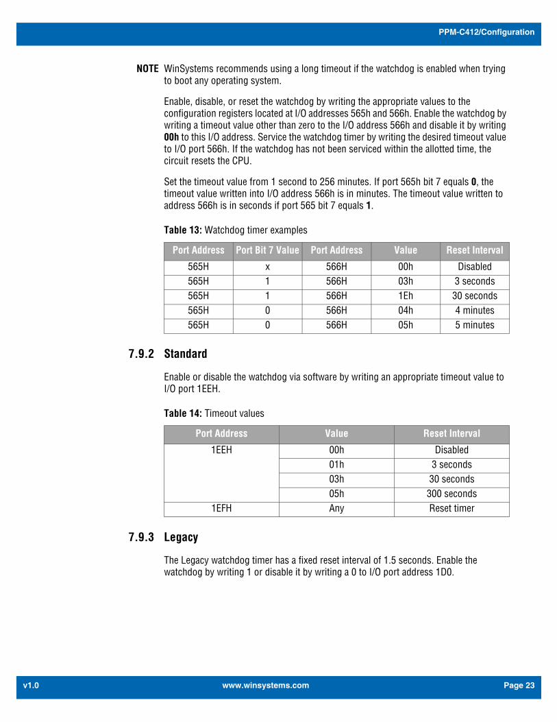
Table 12: Page bits
Page D7 D6 D5-D0
Page 0 0 0 1/0 Page 1 0 1 1/0 Page 2 1 0 1/0 Page 3 1 1 1/0
www.winsystems.com Page 22
PPM-C412/Configuration
v1.0
NOTE WinSystems recommends using a long timeout if the watchdog is enabled when trying to boot any operating system.
Enable, disable, or reset the watchdog by writing the appropriate values to the configuration registers located at I/O addresses 565h and 566h. Enable the watchdog by writing a timeout value other than zero to the I/O address 566h and disable it by writing 00h to this I/O address. Service the watchdog timer by writing the desired timeout value to I/O port 566h. If the watchdog has not been serviced within the allotted time, the circuit resets the CPU.
Set the timeout value from 1 second to 256 minutes. If port 565h bit 7 equals 0, the timeout value written into I/O address 566h is in minutes. The timeout value written to address 566h is in seconds if port 565 bit 7 equals 1.
7.9.2 Standard
Enable or disable the watchdog via software by writing an appropriate timeout value to I/O port 1EEH.
7.9.3 Legacy
The Legacy watchdog timer has a fixed reset interval of 1.5 seconds. Enable the watchdog by writing 1 or disable it by writing a 0 to I/O port address 1D0.
Table 13: Watchdog timer examples
Port Address Port Bit 7 Value Port Address Value Reset Interval
565H x 566H 00h Disabled565H 1 566H 03h 3 seconds565H 1 566H 1Eh 30 seconds565H 0 566H 04h 4 minutes565H 0 566H 05h 5 minutes
Table 14: Timeout values
Port Address Value Reset Interval
1EEH 00h Disabled01h 3 seconds03h 30 seconds05h 300 seconds
1EFH Any Reset timer
www.winsystems.com Page 23
PPM-C412/Configuration
v1.0
7.10 Real-time Clock/Calendar
A real-time clock is used as the AT-compatible clock/calendar. It supports a number of features including periodic and alarm interrupt capabilities. In addition to the time and date-keeping functions, the system configuration is kept in CMOS RAM contained within the clock section. A battery must be enabled for the real-time clock to retain time and date during a power down.
7.11 SP1 Speaker
An on-board speaker, SP1, is available for sound generation.
7.12 Connectors
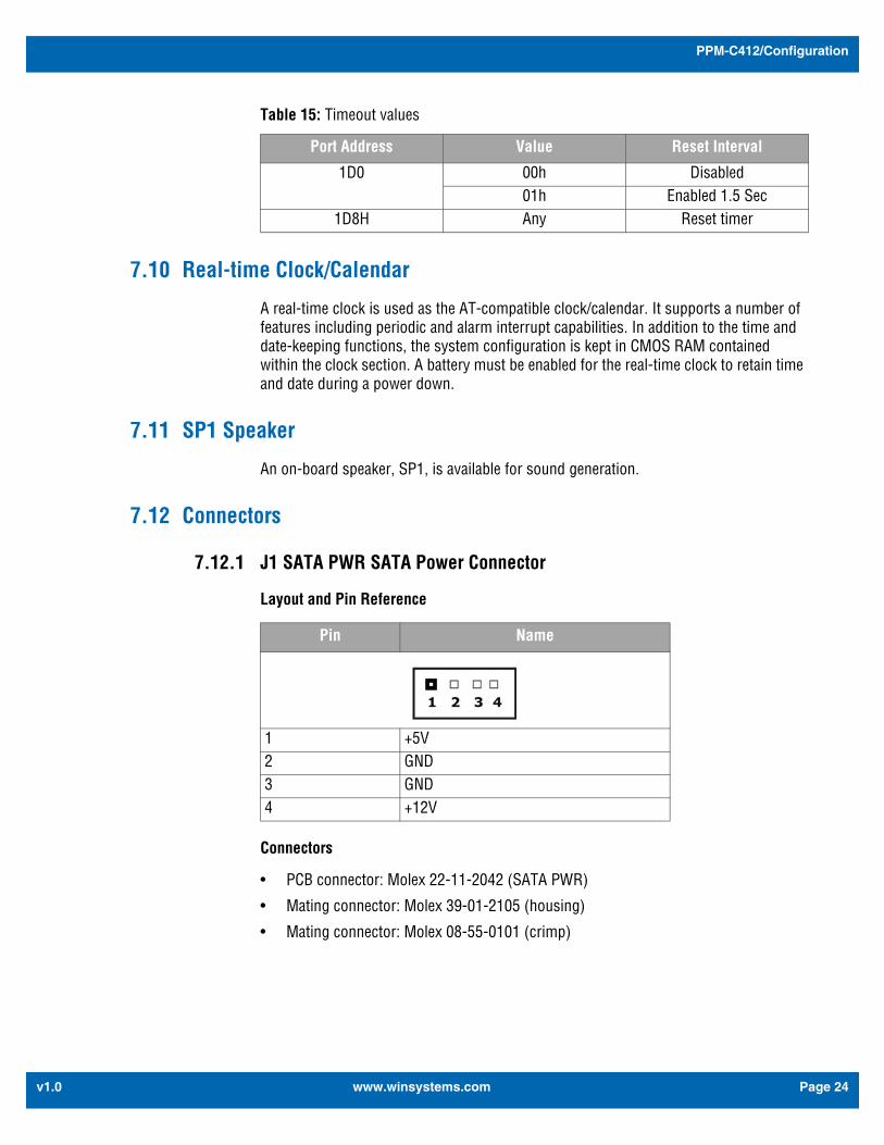
7.12.1 J1 SATA PWR SATA Power Connector
Layout and Pin Reference
Connectors
• PCB connector: Molex 22-11-2042 (SATA PWR)
• Mating connector: Molex 39-01-2105 (housing)
• Mating connector: Molex 08-55-0101 (crimp)
Table 15: Timeout values
Port Address Value Reset Interval
1D0 00h Disabled01h Enabled 1.5 Sec
1D8H Any Reset timer
Pin Name
1 +5V2 GND3 GND4 +12V
www.winsystems.com Page 24
PPM-C412/Configuration
v1.0
7.12.2 J3 Power and Reset
Power is applied to the PPM-C412 through the 8-pin Molex connector at J3. The definitions for J3 are listed in the table below.
An optional reset button can be connected between pin 8 and ground. Momentary contact between pin 8 and ground causes the PPM-C412 to reset. There is also a reset push-button supplied on the CBL-251-G-1-1.5 Multi-I/O cable. This cable is includes in the cable set CBL-SET-412-1.
Power Fail Reset
A precision voltage comparator monitors the +5V status. Upon detection of an out-of-tolerance condition, the board is reset. This action is critically important in the event of brown-out or power fail conditions. The reset circuit also ensures that the power is nominal before releasing reset. A reset condition occurs when VCC drops between 4.6V and 4.75V for more than 150 ms.
Layout and Pin Reference
Connectors
• PCB connector: Molex 22-12-2084 (PWR)
• Mating connector: Molex 10-11-2083 (housing)
• Mating connector: Molex 08-55-0124 (crimp)
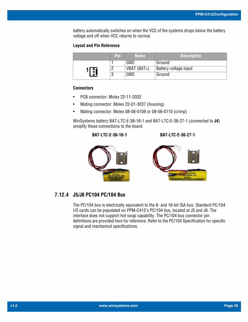
7.12.3 J4 External Battery Connector
An optional external battery, connected to J4, supplies the PPM-C412 board with standby power for the real-time clock and CMOS setup RAM. Extended temperature lithium batteries are available from WinSystems, part numbers:
• BAT-LTC-E-36-16-1
• BAT-LTC-E-36-27-1
A power supervisory circuit contains the voltage sensing circuit and an internal power switch to route the battery or standby voltage to the circuits selected for backup. The
Pin Name Pin Name
1 -12V 5 GND2 +12V 6 GND3 +5V 7 GND4 +5V 8 RESET
www.winsystems.com Page 25
PPM-C412/Configuration
v1.0
battery automatically switches on when the VCC of the systems drops below the battery voltage and off when VCC returns to normal.
Layout and Pin Reference
Connectors
• PCB connector: Molex 22-11-2032
• Mating connector: Molex 22-01-3037 (housing)
• Mating connector: Molex 08-56-0109 or 08-56-0110 (crimp)
WinSystems battery BAT-LTC-E-36-16-1 and BAT-LTC-E-36-27-1 (connected to J4) simplify these connections to the board.
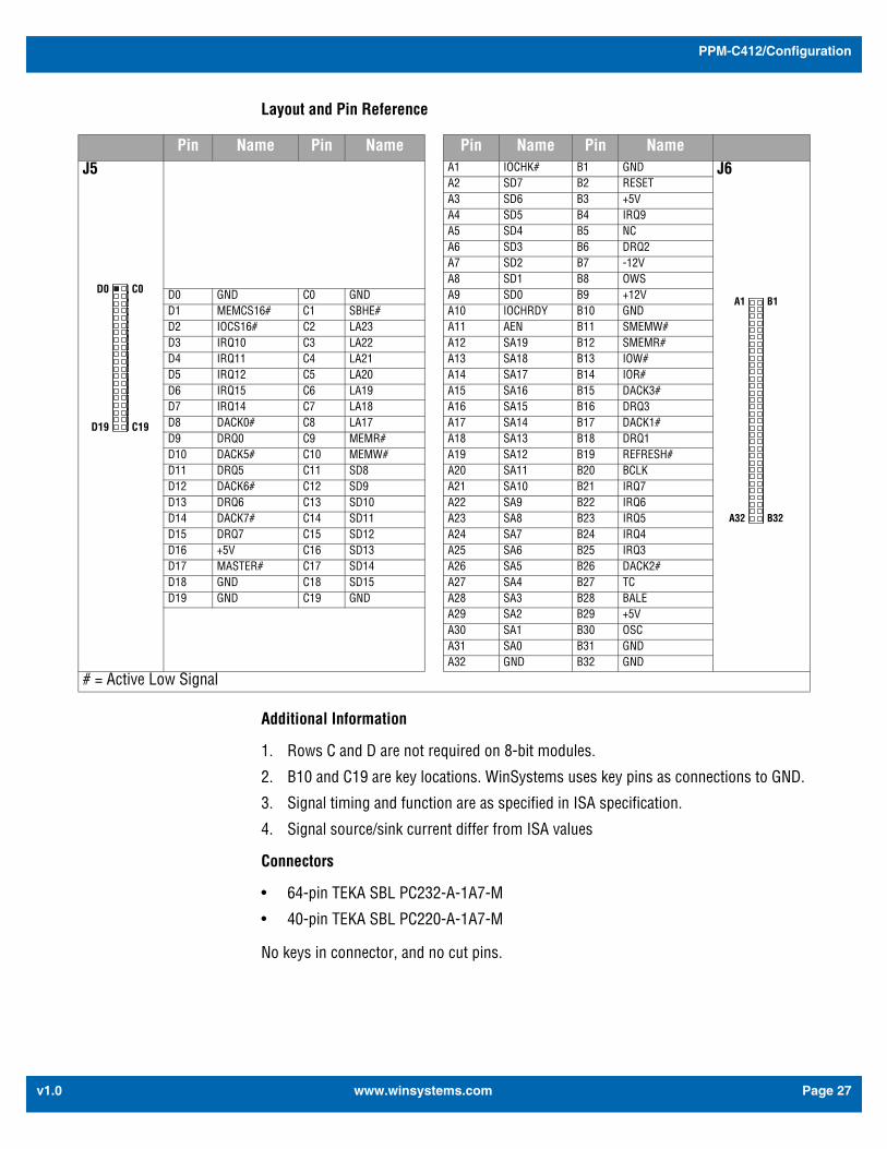
7.12.4 J5/J6 PC104 PC/104 Bus
The PC/104 bus is electrically equivalent to the 8- and 16-bit ISA bus. Standard PC/104 I/O cards can be populated on PPM-C412’s PC/104 bus, located at J5 and J6. The interface does not support hot swap capability. The PC/104 bus connector pin definitions are provided here for reference. Refer to the PC/104 Specification for specific signal and mechanical specifications.
Pin Name Description1 GND Ground2 VBAT (BAT+) Battery voltage input3 GND Ground
BAT-LTC-E-36-27-1BAT-LTC-E-36-16-1
www.winsystems.com Page 26
PPM-C412/Configuration
v1.0
Layout and Pin Reference
Additional Information
1. Rows C and D are not required on 8-bit modules.
2. B10 and C19 are key locations. WinSystems uses key pins as connections to GND.
3. Signal timing and function are as specified in ISA specification.
4. Signal source/sink current differ from ISA values
Connectors
• 64-pin TEKA SBL PC232-A-1A7-M
• 40-pin TEKA SBL PC220-A-1A7-M
No keys in connector, and no cut pins.
Pin Name Pin Name Pin Name Pin NameJ5 A1 IOCHK# B1 GND J6
A2 SD7 B2 RESETA3 SD6 B3 +5VA4 SD5 B4 IRQ9A5 SD4 B5 NCA6 SD3 B6 DRQ2A7 SD2 B7 -12VA8 SD1 B8 OWS
D0 GND C0 GND A9 SD0 B9 +12VD1 MEMCS16# C1 SBHE# A10 IOCHRDY B10 GNDD2 IOCS16# C2 LA23 A11 AEN B11 SMEMW#D3 IRQ10 C3 LA22 A12 SA19 B12 SMEMR#D4 IRQ11 C4 LA21 A13 SA18 B13 IOW#D5 IRQ12 C5 LA20 A14 SA17 B14 IOR#D6 IRQ15 C6 LA19 A15 SA16 B15 DACK3#D7 IRQ14 C7 LA18 A16 SA15 B16 DRQ3D8 DACK0# C8 LA17 A17 SA14 B17 DACK1#D9 DRQ0 C9 MEMR# A18 SA13 B18 DRQ1D10 DACK5# C10 MEMW# A19 SA12 B19 REFRESH#D11 DRQ5 C11 SD8 A20 SA11 B20 BCLKD12 DACK6# C12 SD9 A21 SA10 B21 IRQ7D13 DRQ6 C13 SD10 A22 SA9 B22 IRQ6D14 DACK7# C14 SD11 A23 SA8 B23 IRQ5D15 DRQ7 C15 SD12 A24 SA7 B24 IRQ4D16 +5V C16 SD13 A25 SA6 B25 IRQ3D17 MASTER# C17 SD14 A26 SA5 B26 DACK2#D18 GND C18 SD15 A27 SA4 B27 TCD19 GND C19 GND A28 SA3 B28 BALE
A29 SA2 B29 +5VA30 SA1 B30 OSCA31 SA0 B31 GNDA32 GND B32 GND
# = Active Low Signal
D0
D19
C0
C19
A1
A32
B1
B32
www.winsystems.com Page 27
PPM-C412/Configuration
v1.0
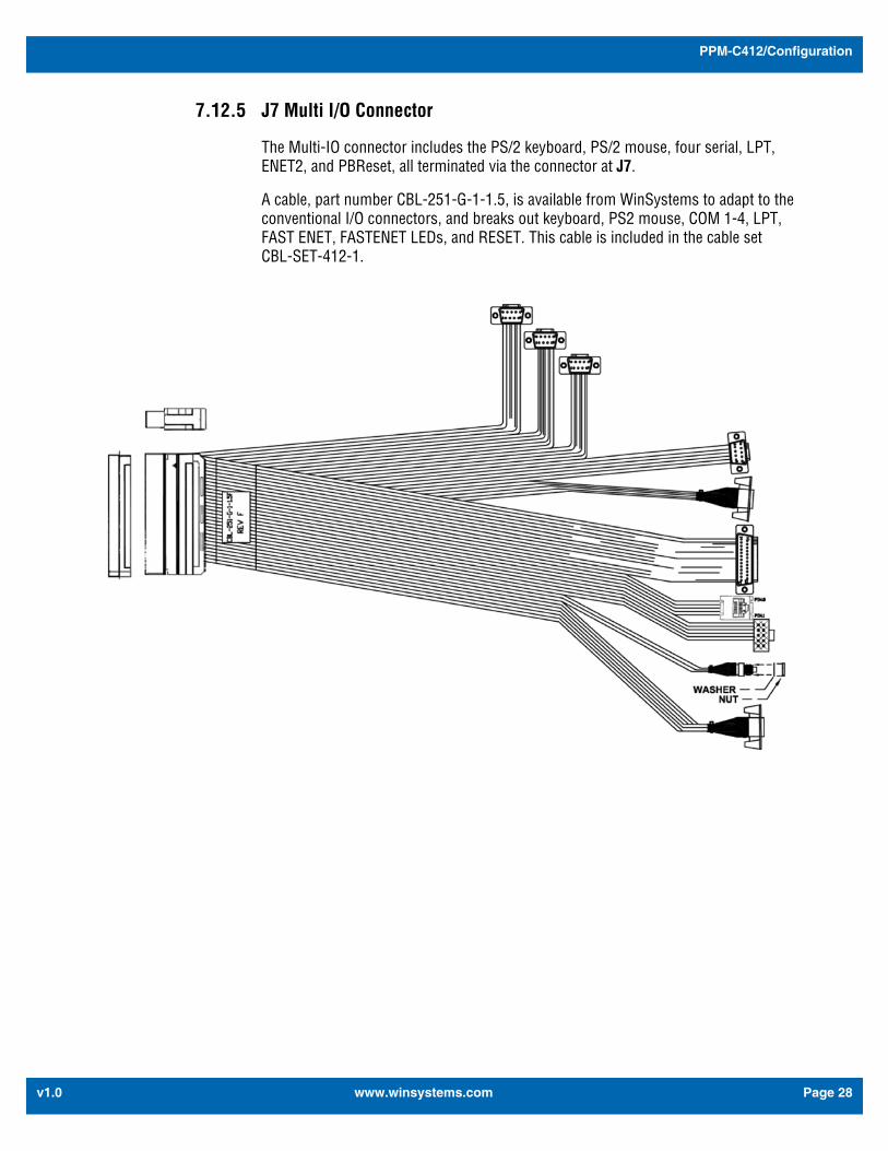
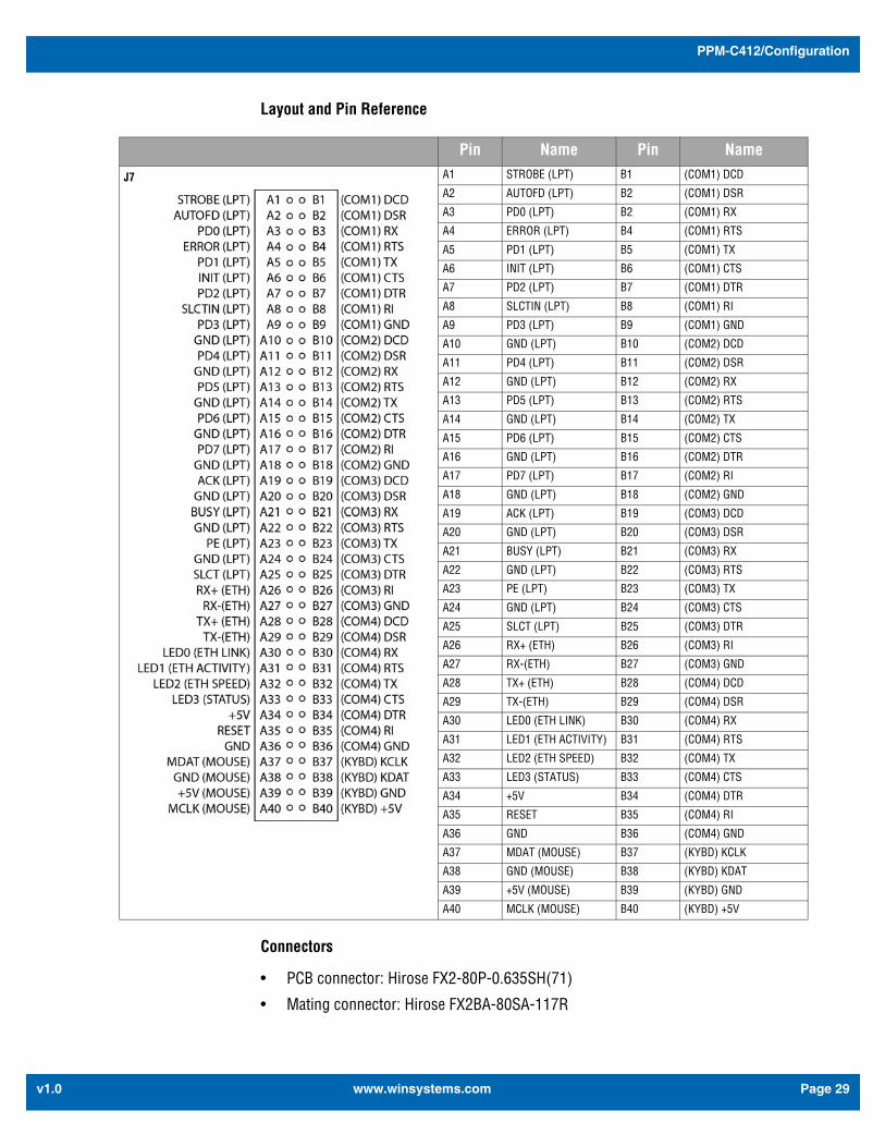
7.12.5 J7 Multi I/O Connector
The Multi-IO connector includes the PS/2 keyboard, PS/2 mouse, four serial, LPT, ENET2, and PBReset, all terminated via the connector at J7.
A cable, part number CBL-251-G-1-1.5, is available from WinSystems to adapt to the conventional I/O connectors, and breaks out keyboard, PS2 mouse, COM 1-4, LPT, FAST ENET, FASTENET LEDs, and RESET. This cable is included in the cable set CBL-SET-412-1.
www.winsystems.com Page 28
PPM-C412/Configuration
v1.0
Layout and Pin Reference
Connectors
• PCB connector: Hirose FX2-80P-0.635SH(71)
• Mating connector: Hirose FX2BA-80SA-117R
Pin Name Pin Name
J7 A1 STROBE (LPT) B1 (COM1) DCD
A2 AUTOFD (LPT) B2 (COM1) DSR
A3 PD0 (LPT) B2 (COM1) RX
A4 ERROR (LPT) B4 (COM1) RTS
A5 PD1 (LPT) B5 (COM1) TX
A6 INIT (LPT) B6 (COM1) CTS
A7 PD2 (LPT) B7 (COM1) DTR
A8 SLCTIN (LPT) B8 (COM1) RI
A9 PD3 (LPT) B9 (COM1) GND
A10 GND (LPT) B10 (COM2) DCD
A11 PD4 (LPT) B11 (COM2) DSR
A12 GND (LPT) B12 (COM2) RX
A13 PD5 (LPT) B13 (COM2) RTS
A14 GND (LPT) B14 (COM2) TX
A15 PD6 (LPT) B15 (COM2) CTS
A16 GND (LPT) B16 (COM2) DTR
A17 PD7 (LPT) B17 (COM2) RI
A18 GND (LPT) B18 (COM2) GND
A19 ACK (LPT) B19 (COM3) DCD
A20 GND (LPT) B20 (COM3) DSR
A21 BUSY (LPT) B21 (COM3) RX
A22 GND (LPT) B22 (COM3) RTS
A23 PE (LPT) B23 (COM3) TX
A24 GND (LPT) B24 (COM3) CTS
A25 SLCT (LPT) B25 (COM3) DTR
A26 RX+ (ETH) B26 (COM3) RI
A27 RX-(ETH) B27 (COM3) GND
A28 TX+ (ETH) B28 (COM4) DCD
A29 TX-(ETH) B29 (COM4) DSR
A30 LED0 (ETH LINK) B30 (COM4) RX
A31 LED1 (ETH ACTIVITY) B31 (COM4) RTS
A32 LED2 (ETH SPEED) B32 (COM4) TX
A33 LED3 (STATUS) B33 (COM4) CTS
A34 +5V B34 (COM4) DTR
A35 RESET B35 (COM4) RI
A36 GND B36 (COM4) GND
A37 MDAT (MOUSE) B37 (KYBD) KCLK
A38 GND (MOUSE) B38 (KYBD) KDAT
A39 +5V (MOUSE) B39 (KYBD) GND
A40 MCLK (MOUSE) B40 (KYBD) +5V
www.winsystems.com Page 29
PPM-C412/Configuration
v1.0
Keyboard
An integrated 80C42 equivalent keyboard controller supports a PS/2 keyboard which is terminated at connector J7. Optionally, a USB keyboard can be connected in addition to, or instead of the standard PS/2 keyboard.
Mouse Interface
A PS/2 mouse port provides connection for a compatible mouse and is terminated at connector J7. Optionally, a USB mouse can be connected in addition to, or instead of the standard PS/2 mouse.
Serial Connectors
Four independent, asynchronous serial channels are on-board. The interface is provided at connector J7, which is an 80-pin, high-density connector. WinSystems offers the cable CBL-251-G-1-1.5 to simplify the connection. This cable is included in the cable set CBL-SET-412-1. Configuration options for RS-232, RS-422, and RS-485 are listed below.
All serial channels are configured as data terminal equipment (DTE). Both the send and receive registers of each channel have a 16-byte FIFO. All serial ports have 16C550-compatible UARTs.
Independent control of transmit, receive, line status, and data set interrupts are on all channels. Each channel is setup to provide internal diagnostics such as loopback and echo mode on the data stream. An independent, software programmable baud rate generator is selectable from 50 to 115.2 kbps. Individual modem handshake control signals are supported for all channels.
RS-232 interface levels are supported on all four serial ports. The RS-232 drivers have a charge pump to generate the plus and minus voltages so that the PPM-C412 only requires +5V to operate.
All COM ports support RS-232 and can be enabled in the BIOS. COM1 and COM2 also have RS-422/RS-485 support. RS-422/485 provides separate balanced transmit and receive signal pairs. For RS-485 multidrop lines, one signal pair can be used for “party line” network structures.
See “BIOS” on page 43 for further details.
COM1 and COM2 Configuration Options
1. Internal loopback
2. RS-422 mode
3. RS-422 mode with auto transmitter enable - (TX Direction = TXD)
4. RS-485 mode with auto transmitter enable - (TX Direction = TXD)
www.winsystems.com Page 30
PPM-C412/Configuration
v1.0
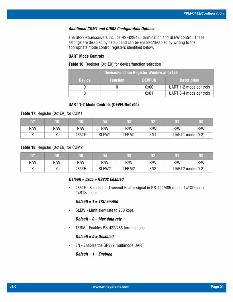
Additional COM1 and COM2 Configuration Options
The SP339 transceivers include RS-422/485 termination and SLEW control. These settings are disabled by default and can be enabled/disabled by writing to the appropriate mode control registers identified below.
UART Mode Controls
UART 1-2 Mode Controls (DEVFUN=0x00)
Default = 0x05 = RS232 Enabled
• 485TE - Selects the Transmit Enable signal in RS-422/485 mode; 1=TXD enable, 0=RTS enable
Default = 1 = TXD enable
• SLEW - Limit slew rate to 250 kbps
Default = 0 = Max data rate
• TERM - Enables RS-422/485 terminations
Default = 0 = Disabled
• EN - Enables the SP339 multimode UART
Default = 1 = Enabled
Table 16: Register (0x1E9) for device/function selection
Device/Function Register Window at 0x1E9
Device Function DEVFUN Description
0 0 0x00 UART 1-2 mode controls0 1 0x01 UART 3-4 mode controls
Table 17: Register (0x1EA) for COM1
D7 D6 D5 D4 D3 D2 D1 D0
R/W R/W R/W R/W R/W R/W R/W R/WX X 485TE SLEW1 TERM1 EN1 UART1 mode (0-3)
Table 18: Register (0x1EB) for COM2
D7 D6 D5 D4 D3 D2 D1 D0
R/W R/W R/W R/W R/W R/W R/W R/WX X 485TE SLEW2 TERM2 EN2 UART2 mode (0-3)
www.winsystems.com Page 31
PPM-C412/Configuration
v1.0
MODE - Selects the communication mode of the serial port (set in BIOS and should be maintained).
Example: Set COM1 to RS-485 Auto with termination and COM2 RS-422 Auto with SKEW:
Write 0x00 to 0x1E9 Points to COM1-2 Mode controls
Write 0x2E to 0x1EA COM1 - 485TE, TERM2, EN1, MODE 2
Write 0x37 to 0x1EB COM2 - 485TE, SLEW2, EN2, MODE 3
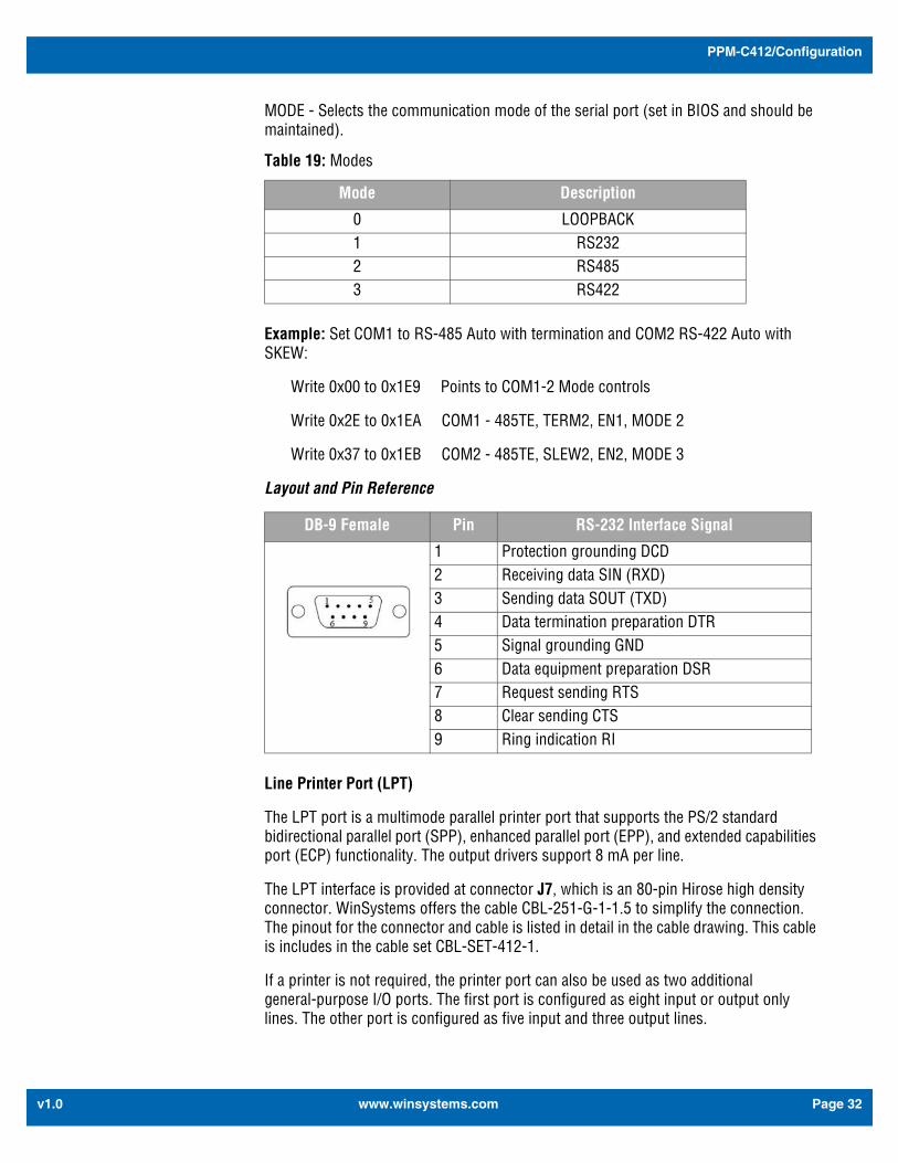
Layout and Pin Reference
Line Printer Port (LPT)
The LPT port is a multimode parallel printer port that supports the PS/2 standard bidirectional parallel port (SPP), enhanced parallel port (EPP), and extended capabilities port (ECP) functionality. The output drivers support 8 mA per line.
The LPT interface is provided at connector J7, which is an 80-pin Hirose high density connector. WinSystems offers the cable CBL-251-G-1-1.5 to simplify the connection. The pinout for the connector and cable is listed in detail in the cable drawing. This cable is includes in the cable set CBL-SET-412-1.
If a printer is not required, the printer port can also be used as two additional general-purpose I/O ports. The first port is configured as eight input or output only lines. The other port is configured as five input and three output lines.
Table 19: Modes
Mode Description
0 LOOPBACK1 RS2322 RS4853 RS422
DB-9 Female Pin RS-232 Interface Signal
1 Protection grounding DCD2 Receiving data SIN (RXD)3 Sending data SOUT (TXD)4 Data termination preparation DTR5 Signal grounding GND6 Data equipment preparation DSR7 Request sending RTS8 Clear sending CTS9 Ring indication RI
www.winsystems.com Page 32
PPM-C412/Configuration
v1.0
Layout and Pin Reference
Fast Ethernet
A DMP Vortex Ethernet controller chip is used for high-speed data transfer. It has auto-negotiation capability for speed, duplex and flow control. It supports IEEE 802.3 10Base-T and 100Base-T.
The Ethernet interface is provided at Multi-I/O connector J7, which is an 80-pin high density connector. WinSystems offers the cable CBL-251-G-1-1.5 to simplify the connection. This cable is included in the cable set CBL-SET-412-1.
The D1 and D2 LEDs provide a visual indication of the link status, network activity and network speed. The yellow Link/Activity LED at D1 is lit when a valid connection is detected and blinks when activity is detected on the wire.The red LED at D2 is on if a 100Base-T link is detected and off if a 10Base-T link is detected.
Ethernet activity signals are also provided at connector J7 to allow optional status LEDs to be mounted off-board. The Ethernet activity signals are active low and require an external resistor to limit current to 12-16 mA.
7.12.6 J103 10/100/1000 Mbps Ethernet
An Intel I210 32-bit PCIe Gigabit Ethernet controller chip is used for high-speed data transfer. It has auto-negotiation capability for speed, duplex and flow control. It supports IEEE 802.3 10Base-T, 100Base-T, and 1000Base-T.
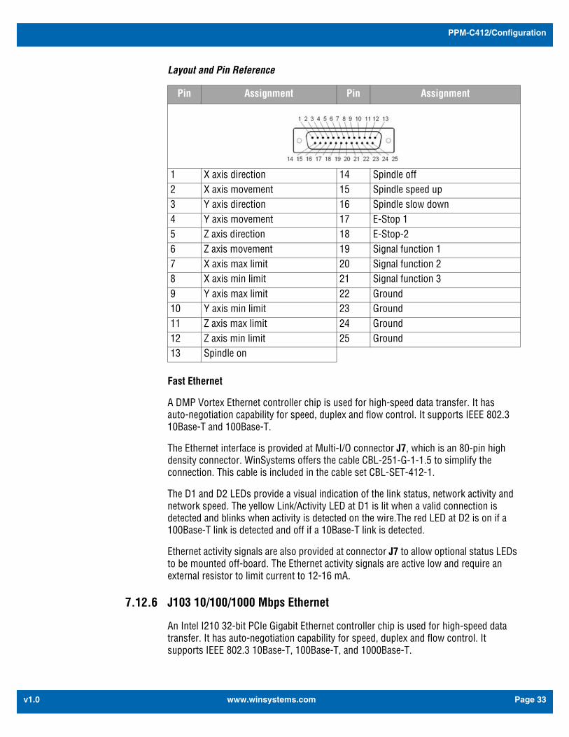
Pin Assignment Pin Assignment
1 X axis direction 14 Spindle off2 X axis movement 15 Spindle speed up3 Y axis direction 16 Spindle slow down4 Y axis movement 17 E-Stop 15 Z axis direction 18 E-Stop-26 Z axis movement 19 Signal function 17 X axis max limit 20 Signal function 28 X axis min limit 21 Signal function 39 Y axis max limit 22 Ground10 Y axis min limit 23 Ground11 Z axis max limit 24 Ground12 Z axis min limit 25 Ground13 Spindle on
www.winsystems.com Page 33
PPM-C412/Configuration
v1.0
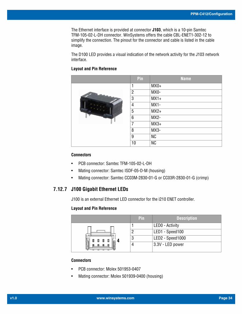
The Ethernet interface is provided at connector J103, which is a 10-pin Samtec TFM-105-02-L-DH connector. WinSystems offers the cable CBL-ENET1-302-12 to simplify the connection. The pinout for the connector and cable is listed in the cable image.
The D100 LED provides a visual indication of the network activity for the J103 network interface.
Layout and Pin Reference
Connectors
• PCB connector: Samtec TFM-105-02-L-DH
• Mating connector: Samtec ISDF-05-D-M (housing)
• Mating connector: Samtec CC03M-2830-01-G or CC03R-2830-01-G (crimp)
7.12.7 J100 Gigabit Ethernet LEDs
J100 is an external Ethernet LED connector for the i210 ENET controller.
Layout and Pin Reference
Connectors
• PCB connector: Molex 501953-0407
• Mating connector: Molex 501939-0400 (housing)
Pin Name
1 MX0+2 MX0-3 MX1+4 MX1-5 MX2+6 MX2-7 MX3+8 MX3-9 NC10 NC
Pin Description
1 LED0 - Activity2 LED1 - Speed1003 LED2 - Speed10004 3.3V - LED power
4
www.winsystems.com Page 34
PPM-C412/Configuration
v1.0
• Mating connector: Molex 501334 (terminal)
7.12.8 J8 CompactFlash Socket
The PPM-C412 supports solid state CompactFlash storage devices for applications where the environment is too harsh for mechanical hard disks.
The CompactFlash socket at J8 supports modules with TrueIDE support. WinSystems offers industrial grade CompactFlash modules that provide high performance and extended temperature operation (-40 to +85°C). An IDE activity LED is present at D3.
7.12.9 J9 PC/104-Plus (PCI-104) Bus
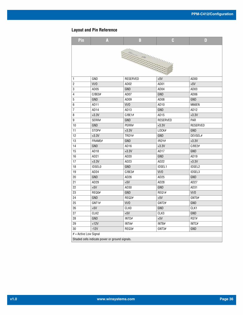
The PPM-C412 supports peripheral expansion using the PC/104-Plus expansion (PC/104 in addition to PCI-104). The PCI-104 connector at J9 supports up to three PCI-104 or PC/104-Plus modules stacked onto the PPM-C412. PCI-104 modules should be attached and configured beginning at slot 1. The PCI-104 bus pin definitions are shown here for reference purposes only. Refer to the PC/104 Specification for signal definitions, timing, and mechanical details.
www.winsystems.com Page 35
PPM-C412/Configuration
v1.0
Layout and Pin Reference
Pin A B C D
1 GND RESERVED +5V AD00
2 VI/O AD02 AD01 +5V
3 AD05 GND AD04 AD03
4 C/BE0# AD07 GND AD06
5 GND AD09 AD08 GND
6 AD11 VI/O AD10 M66EN
7 AD14 AD13 GND AD12
8 +3.3V C/BE1# AD15 +3.3V
9 SERR# GND RESERVED PAR
10 GND PERR# +3.3V RESERVED
11 STOP# +3.3V LOCK# GND
12 +3.3V TRDY# GND DEVSEL#
13 FRAME# GND IRDY# +3.3V
14 GND AD16 +3.3V C/BE2#
15 AD18 +3.3V AD17 GND
16 AD21 AD20 GND AD19
17 +3.3V AD23 AD22 +3.3V
18 IDSEL0 GND IDSEL1 IDSEL2
19 AD24 C/BE3# VI/O IDSEL3
20 GND AD26 AD25 GND
21 AD29 +5V AD28 AD27
22 +5V AD30 GND AD31
23 REQ0# GND REQ1# VI/O
24 GND REQ2# +5V GNT0#
25 GNT1# VI/O GNT2# GND
26 +5V CLK0 GND CLK1
27 CLK2 +5V CLK3 GND
28 GND INTD# +5V RST#
29 +12V INTA# INTB# INTC#
30 -12V REQ3# GNT3# GND
# = Active Low Signal
Shaded cells indicate power or ground signals.
www.winsystems.com Page 36
PPM-C412/Configuration
v1.0
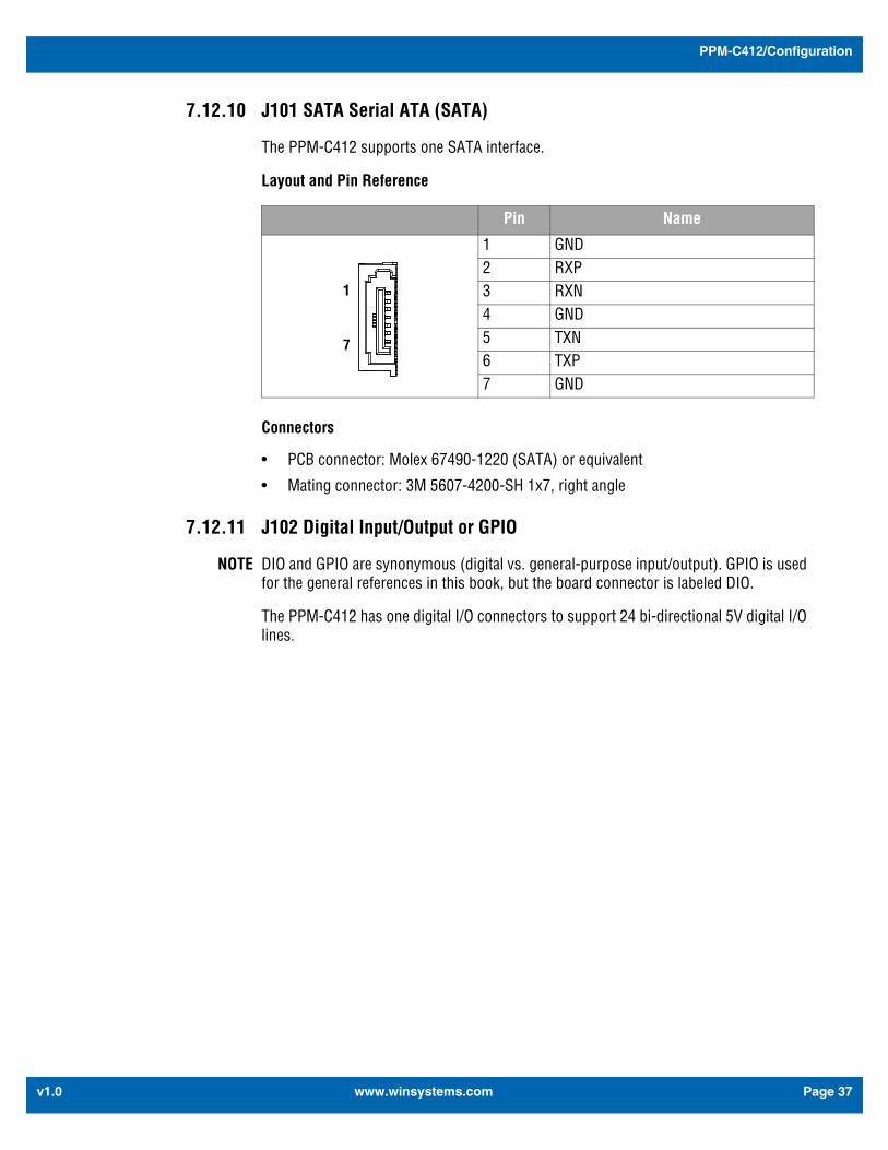
7.12.10 J101 SATA Serial ATA (SATA)
The PPM-C412 supports one SATA interface.
Layout and Pin Reference
Connectors
• PCB connector: Molex 67490-1220 (SATA) or equivalent
• Mating connector: 3M 5607-4200-SH 1x7, right angle
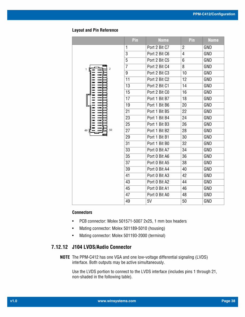
7.12.11 J102 Digital Input/Output or GPIO
NOTE DIO and GPIO are synonymous (digital vs. general-purpose input/output). GPIO is used for the general references in this book, but the board connector is labeled DIO.
The PPM-C412 has one digital I/O connectors to support 24 bi-directional 5V digital I/O lines.
Pin Name
1 GND2 RXP3 RXN4 GND5 TXN6 TXP7 GND
7
1
www.winsystems.com Page 37
PPM-C412/Configuration
v1.0
Layout and Pin Reference
Connectors
• PCB connector: Molex 501571-5007 2x25, 1 mm box headers
• Mating connector: Molex 501189-5010 (housing)
• Mating connector: Molex 501193-2000 (terminal)
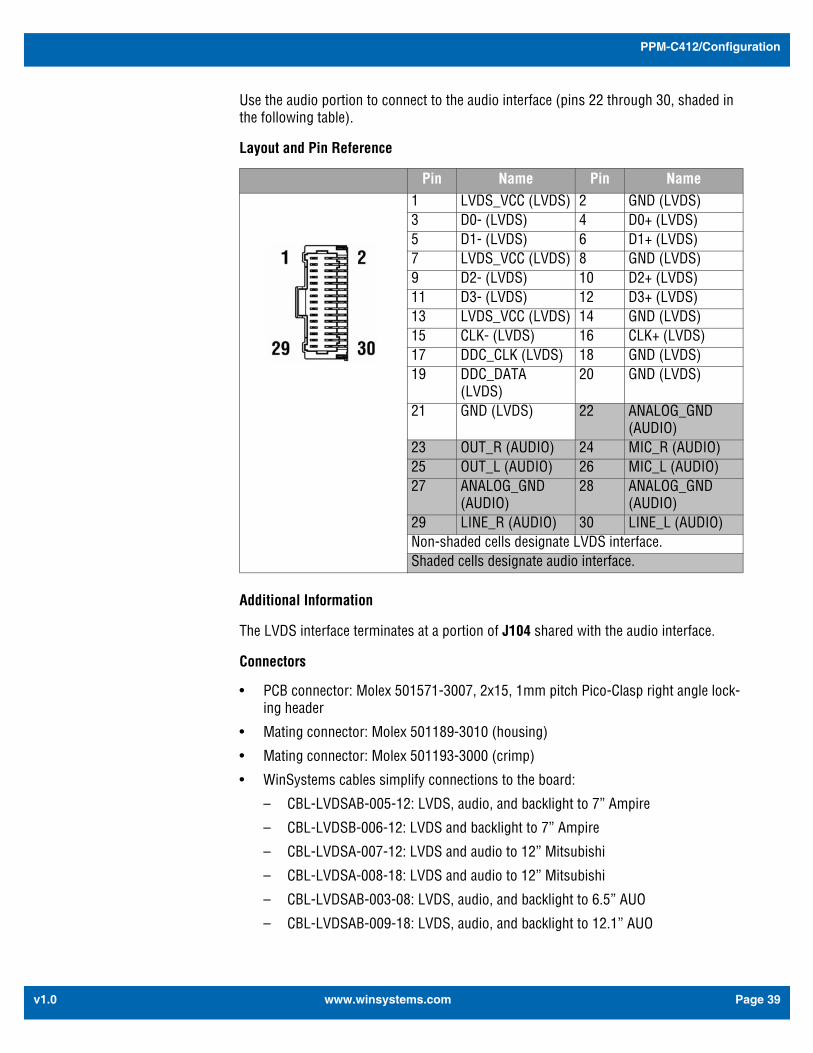
7.12.12 J104 LVDS/Audio Connector
NOTE The PPM-C412 has one VGA and one low-voltage differential signaling (LVDS) interface. Both outputs may be active simultaneously.
Use the LVDS portion to connect to the LVDS interface (includes pins 1 through 21, non-shaded in the following table).
Pin Name Pin Name
1 Port 2 Bit C7 2 GND3 Port 2 Bit C6 4 GND5 Port 2 Bit C5 6 GND7 Port 2 Bit C4 8 GND9 Port 2 Bit C3 10 GND11 Port 2 Bit C2 12 GND13 Port 2 Bit C1 14 GND15 Port 2 Bit C0 16 GND17 Port 1 Bit B7 18 GND19 Port 1 Bit B6 20 GND21 Port 1 Bit B5 22 GND23 Port 1 Bit B4 24 GND25 Port 1 Bit B3 26 GND27 Port 1 Bit B2 28 GND29 Port 1 Bit B1 30 GND31 Port 1 Bit B0 32 GND33 Port 0 Bit A7 34 GND35 Port 0 Bit A6 36 GND37 Port 0 Bit A5 38 GND39 Port 0 Bit A4 40 GND41 Port 0 Bit A3 42 GND43 Port 0 Bit A2 44 GND45 Port 0 Bit A1 46 GND47 Port 0 Bit A0 48 GND49 5V 50 GND
49 50
21
www.winsystems.com Page 38
PPM-C412/Configuration
v1.0
Use the audio portion to connect to the audio interface (pins 22 through 30, shaded in the following table).
Layout and Pin Reference
Additional Information
The LVDS interface terminates at a portion of J104 shared with the audio interface.
Connectors
• PCB connector: Molex 501571-3007, 2x15, 1mm pitch Pico-Clasp right angle lock-ing header
• Mating connector: Molex 501189-3010 (housing)
• Mating connector: Molex 501193-3000 (crimp)
• WinSystems cables simplify connections to the board:
– CBL-LVDSAB-005-12: LVDS, audio, and backlight to 7” Ampire
– CBL-LVDSB-006-12: LVDS and backlight to 7” Ampire
– CBL-LVDSA-007-12: LVDS and audio to 12” Mitsubishi
– CBL-LVDSA-008-18: LVDS and audio to 12” Mitsubishi
– CBL-LVDSAB-003-08: LVDS, audio, and backlight to 6.5” AUO
– CBL-LVDSAB-009-18: LVDS, audio, and backlight to 12.1” AUO
Pin Name Pin Name1 LVDS_VCC (LVDS) 2 GND (LVDS)3 D0- (LVDS) 4 D0+ (LVDS)5 D1- (LVDS) 6 D1+ (LVDS)7 LVDS_VCC (LVDS) 8 GND (LVDS)9 D2- (LVDS) 10 D2+ (LVDS)11 D3- (LVDS) 12 D3+ (LVDS)13 LVDS_VCC (LVDS) 14 GND (LVDS)15 CLK- (LVDS) 16 CLK+ (LVDS)17 DDC_CLK (LVDS) 18 GND (LVDS)19 DDC_DATA
(LVDS)20 GND (LVDS)
21 GND (LVDS) 22 ANALOG_GND (AUDIO)
23 OUT_R (AUDIO) 24 MIC_R (AUDIO)25 OUT_L (AUDIO) 26 MIC_L (AUDIO)27 ANALOG_GND
(AUDIO)28 ANALOG_GND
(AUDIO)29 LINE_R (AUDIO) 30 LINE_L (AUDIO)Non-shaded cells designate LVDS interface.Shaded cells designate audio interface.
www.winsystems.com Page 39
PPM-C412/Configuration
v1.0
– CBL-SPL-001-14: LVDS and audio to unterminated LVDS with audio jacks (shown)
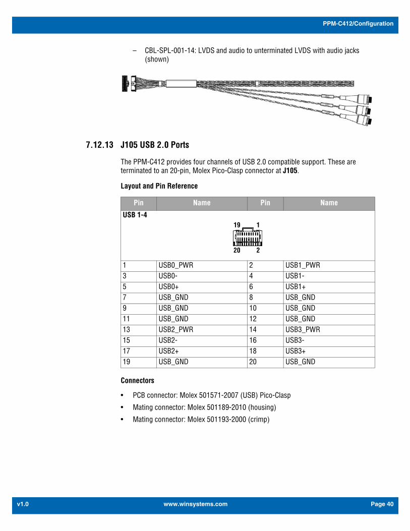
7.12.13 J105 USB 2.0 Ports
The PPM-C412 provides four channels of USB 2.0 compatible support. These are terminated to an 20-pin, Molex Pico-Clasp connector at J105.
Layout and Pin Reference
Connectors
• PCB connector: Molex 501571-2007 (USB) Pico-Clasp
• Mating connector: Molex 501189-2010 (housing)
• Mating connector: Molex 501193-2000 (crimp)
Pin Name Pin Name
USB 1-4
1 USB0_PWR 2 USB1_PWR3 USB0- 4 USB1-5 USB0+ 6 USB1+7 USB_GND 8 USB_GND9 USB_GND 10 USB_GND11 USB_GND 12 USB_GND13 USB2_PWR 14 USB3_PWR15 USB2- 16 USB3-17 USB2+ 18 USB3+19 USB_GND 20 USB_GND
19 1
20 2
www.winsystems.com Page 40
PPM-C412/Configuration
v1.0
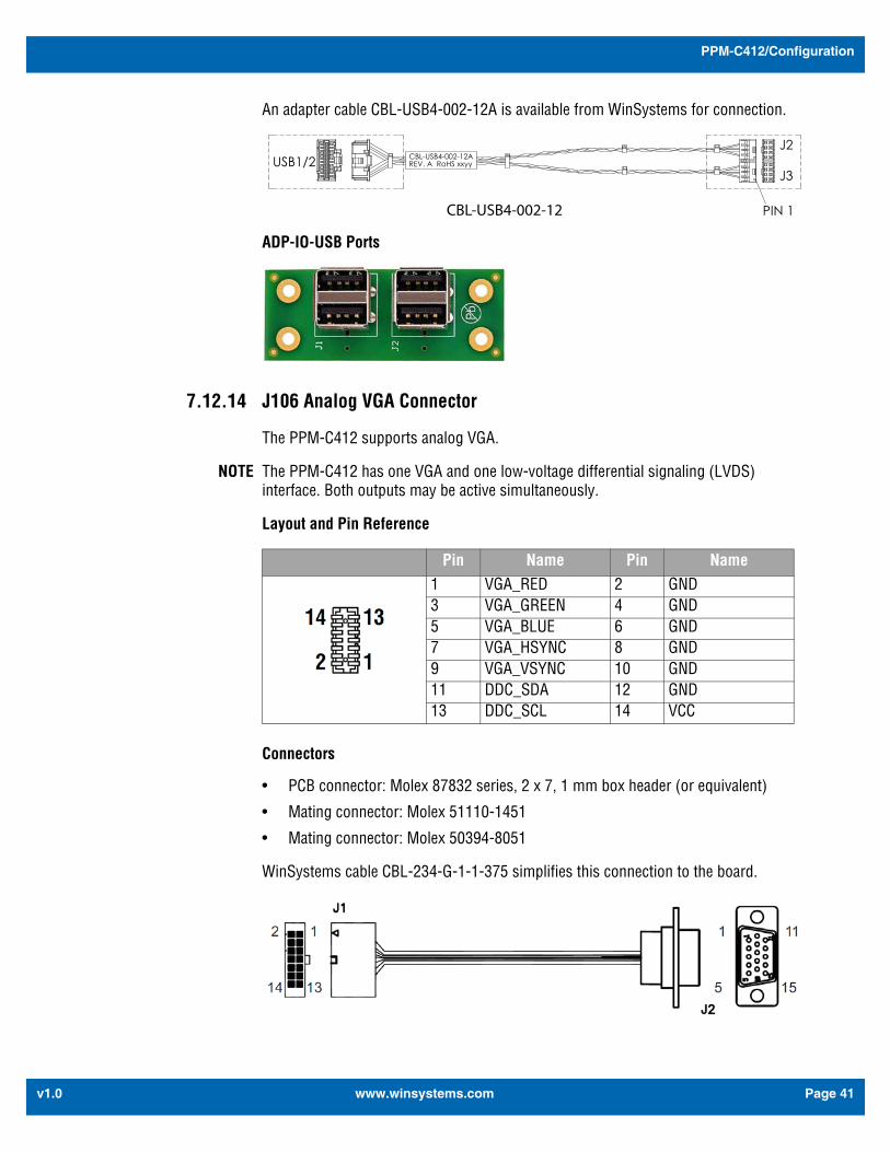
An adapter cable CBL-USB4-002-12A is available from WinSystems for connection.
ADP-IO-USB Ports
7.12.14 J106 Analog VGA Connector
The PPM-C412 supports analog VGA.
NOTE The PPM-C412 has one VGA and one low-voltage differential signaling (LVDS) interface. Both outputs may be active simultaneously.
Layout and Pin Reference
Connectors
• PCB connector: Molex 87832 series, 2 x 7, 1 mm box header (or equivalent)
• Mating connector: Molex 51110-1451
• Mating connector: Molex 50394-8051
WinSystems cable CBL-234-G-1-1-375 simplifies this connection to the board.
USB1/2J2
J3CBL-USB4-002-12AREV. A RoHS xxyy
PIN 1CBL-USB4-002-12
Pin Name Pin Name1 VGA_RED 2 GND3 VGA_GREEN 4 GND5 VGA_BLUE 6 GND7 VGA_HSYNC 8 GND9 VGA_VSYNC 10 GND11 DDC_SDA 12 GND13 DDC_SCL 14 VCC
www.winsystems.com Page 41
PPM-C412/Configuration
v1.0
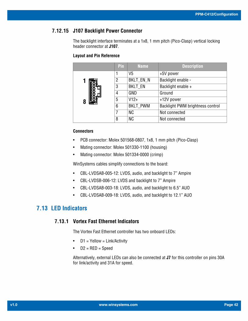
7.12.15 J107 Backlight Power Connector
The backlight interface terminates at a 1x8, 1 mm pitch (Pico-Clasp) vertical locking header connector at J107.
Layout and Pin Reference
Connectors
• PCB connector: Molex 501568-0807, 1x8, 1 mm pitch (Pico-Clasp)
• Mating connector: Molex 501330-1100 (housing)
• Mating connector: Molex 501334-0000 (crimp)
WinSystems cables simplify connections to the board:
• CBL-LVDSAB-005-12: LVDS, audio, and backlight to 7” Ampire
• CBL-LVDSB-006-12: LVDS and backlight to 7” Ampire
• CBL-LVDSAB-003-18: LVDS, audio, and backlight to 6.5” AUO
• CBL-LVDSAB-009-18: LVDS, audio, and backlight to 12.1” AUO
7.13 LED Indicators
7.13.1 Vortex Fast Ethernet Indicators
The Vortex Fast Ethernet controller has two onboard LEDs:
• D1 = Yellow = Link/Activity
• D2 = RED = Speed
Alternatively, external LEDs can also be connected at J7 for this controller on pins 30A for link/activity and 31A for speed.
Pin Name Description
1 V5 +5V power2 BKLT_EN_N Backlight enable -3 BKLT_EN Backlight enable +4 GND Ground5 V12+ +12V power6 BKLT_PWM Backlight PWM brightness control7 NC Not connected8 NC Not connected
www.winsystems.com Page 42
PPM-C412/BIOS
v1.0
7.13.2 D6 Status LED
A green status LED is populated on the board at D6 which can be used for any application specific purpose. The LED can be turned on in software by writing a 1 to I/O port 1EDH. The LED can be turned off by writing a 0 to 1EDH.
7.13.3 i210T Gigabit Ethernet Indicator
The i210T Gigabit Ethernet controller has one onboard LED:
• D100 = Green = Link/activity
Alternatively, external LEDs can also be connected at J100 for this controller.
8. BIOS
8.1 General Information
The PPM-C412 includes BIOS from AMI Software, Inc. to ensure full compatibility with PC operating systems and software. The basic system configuration is stored in battery backed CMOS RAM within the clock/calendar. As an alternative, the CMOS configuration may be stored in EEPROM for operation without a battery. For more information of CMOS configuration, see “BIOS Setting Storage Options” on page 53. Access to this setup information is via the Setup Utility in the BIOS.
8.2 Entering Setup
To enter setup, power up the computer and press Delete when either the splash screen is displayed or when the Press DELETE for Setup message is displayed. It may take a few seconds before the main setup menu screen is displayed.
8.3 Navigating the Menus
Use the Up and Down arrow keys to move among the selections and press Enter when a selection is highlighted to enter a sub-menu or to see a list of choices. Pressing the letter corresponding to each menu option is a shortcut that opens the next dialogue box with one key press.
Following are images of each menu screen in the default configuration along with a brief description of each option where applicable. Available options are listed in reference tables. Menu values shown in bold typeface are factory defaults.
8.4 BIOS Splash Screen
Custom BIOS splash screens can be accommodated for OEM customers. Contact an Application Engineer for details.
www.winsystems.com Page 43
PPM-C412/BIOS
v1.0
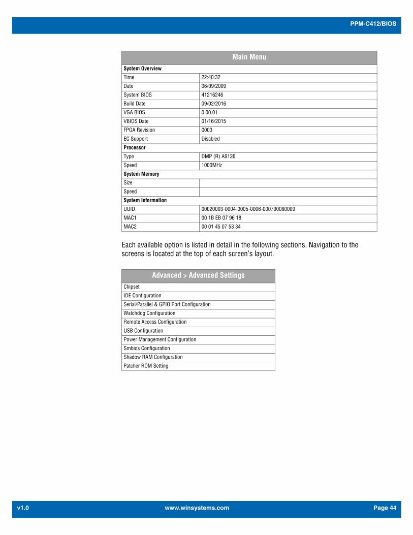
Each available option is listed in detail in the following sections. Navigation to the screens is located at the top of each screen’s layout.
Main MenuSystem Overview
Time 22:40:32
Date 06/09/2009
System BIOS 41216246
Build Date 09/02/2016
VGA BIOS 0.00.01
VBIOS Date 01/16/2015
FPGA Revision 0003
EC Support Disabled
Processor
Type DMP (R) A9126
Speed 1000MHz
System Memory
Size
Speed
System Information
UUID 00020003-0004-0005-0006-000700080009
MAC1 00 1B EB 07 96 18
MAC2 00 01 45 07 53 34
Advanced > Advanced SettingsChipset
IDE Configuration
Serial/Parallel & GPIO Port Configuration
Watchdog Configuration
Remote Access Configuration
USB Configuration
Power Management Configuration
Smbios Configuration
Shadow RAM Configuration
Patcher ROM Setting
www.winsystems.com Page 44
PPM-C412/BIOS
v1.0
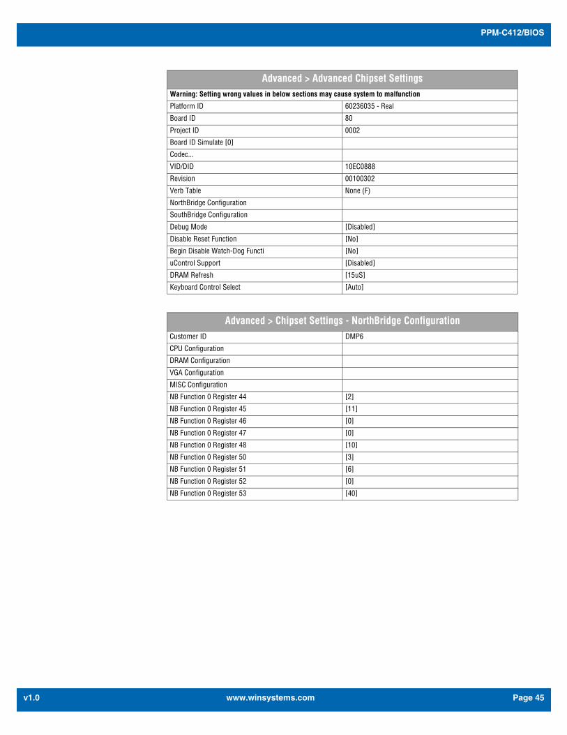
Advanced > Advanced Chipset SettingsWarning: Setting wrong values in below sections may cause system to malfunction
Platform ID 60236035 - Real
Board ID 80
Project ID 0002
Board ID Simulate [0]
Codec...
VID/DID 10EC0888
Revision 00100302
Verb Table None (F)
NorthBridge Configuration
SouthBridge Configuration
Debug Mode [Disabled]
Disable Reset Function [No]
Begin Disable Watch-Dog Functi [No]
uControl Support [Disabled]
DRAM Refresh [15uS]
Keyboard Control Select [Auto]
Advanced > Chipset Settings - NorthBridge ConfigurationCustomer ID DMP6
CPU Configuration
DRAM Configuration
VGA Configuration
MISC Configuration
NB Function 0 Register 44 [2]
NB Function 0 Register 45 [11]
NB Function 0 Register 46 [0]
NB Function 0 Register 47 [0]
NB Function 0 Register 48 [10]
NB Function 0 Register 50 [3]
NB Function 0 Register 51 [6]
NB Function 0 Register 52 [0]
NB Function 0 Register 53 [40]
www.winsystems.com Page 45
PPM-C412/BIOS
v1.0
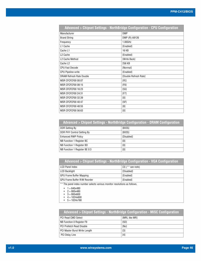
Advanced > Chipset Settings - NorthBridge Configuration - CPU ConfigurationManufacturer DMP
Brand String DMP (R) A9126
Frequency 1.00GHz
L1 Cache [Enabled]
Cache L1 16 KB
L2 Cache [Enabled]
L2 Cache Method [Write Back]
Cache L2 256 KB
CPU Fast Decode [Normal]
CPU Pipeline-write [Enabled]
DRAM Refresh Rate Double [Double Refresh Rate]
MSR CFCFCF00 00:07 [FE]
MSR CFCFCF00 08:15 [F0]
MSR CFCFCF00 16:23 [55]
MSR CFCFCF00 24:31 [F7]
MSR CFCFCF00 32;39 [0]
MSR CFCFCF00 40:47 [5F]
MSR CFCFCF00 48:55 [8]
MSR CFCFCF00 56:63 [0]
Advanced > Chipset Settings - NorthBridge Configuration - DRAM ConfigurationDDR Setting By [BIOS]
DDR PHY Control Setting By [BIOS]
Enhanced RWP Policy [Disabled]
NB Function 1 Register BC [0]
NB Function 1 Register BD [0]
NB Function 1 Register BE 0:3 [0]
Advanced > Chipset Settings - NorthBridge Configuration - VGA ConfigurationLCD Panel Index [3] (** see note)
LCD Backlight [Disabled]
GPU Frame Buffer Mapping [Enabled]
GPU Frame Buffer R/W Reorder [Enabled]
** The panel index number selects various monitor resolutions as follows.
• 1 = 640x480• 2 = 800x480• 3 = 800x600• 4 = 1024x600• 5 = 1024x768
Advanced > Chipset Settings - NorthBridge Configuration - MISC ConfigurationPCI Read CMD Select [MRL like MR]
NB Function 0 Register F9 [5D]
PCI Prefetch Read Disable [No]
PCI Master Burst Write Length [3]
PCI Delay Line [4]
www.winsystems.com Page 46
PPM-C412/BIOS
v1.0
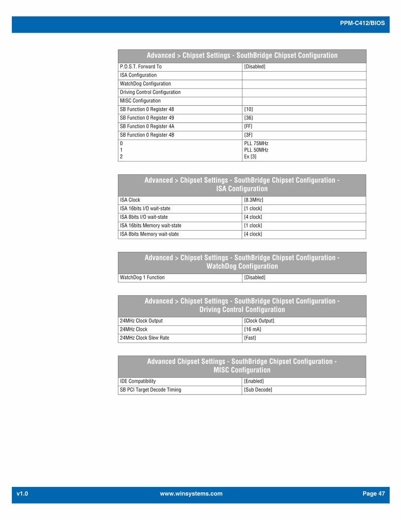
Advanced > Chipset Settings - SouthBridge Chipset ConfigurationP.O.S.T. Forward To [Disabled]
ISA Configuration
WatchDog Configuration
Driving Control Configuration
MISC Configuration
SB Function 0 Register 48 [10]
SB Function 0 Register 49 [36]
SB Function 0 Register 4A [FF]
SB Function 0 Register 4B [3F]
0 12
PLL 75MHz PLL 50MHz Ex [3]
Advanced > Chipset Settings - SouthBridge Chipset Configuration - ISA Configuration
ISA Clock [8.3MHz]
ISA 16bits I/O wait-state [1 clock]
ISA 8bits I/O wait-state [4 clock]
ISA 16bits Memory wait-state [1 clock]
ISA 8bits Memory wait-state [4 clock]
Advanced > Chipset Settings - SouthBridge Chipset Configuration - WatchDog Configuration
WatchDog 1 Function [Disabled]
Advanced > Chipset Settings - SouthBridge Chipset Configuration - Driving Control Configuration
24MHz Clock Output [Clock Output]
24MHz Clock [16 mA]
24MHz Clock Slew Rate [Fast]
Advanced Chipset Settings - SouthBridge Chipset Configuration - MISC Configuration
IDE Compatibility [Enabled]
SB PCI Target Decode Timing [Sub Decode]
www.winsystems.com Page 47
PPM-C412/BIOS
v1.0
Advanced > IDE ConfigurationOnBoard PCI IDE Controller [Both]
Primary IDE Master [Hard Disk]
Secondary IDE Master [Not Detected]
Hard Disk Write Protect [Disabled]
IDE Detect Timeout (Sec) [35]
Hard Disk Delay [Disabled]
OnBoard IDE Operate Mode [Native Mode]
Not program PIO mode [Disabled]
SATA PHY Speed [Auto]
Advanced > Serial/Parallel & GPIO Port ConfigurationSB Serial Port 1 [3F8]
Serial Port IRQ 1 [IRQ4]
Serial Port Baud Rate [115200 BPS]
Serial Port 1 Mode [RS232]
SB Serial Port 2 [2F8]
Serial Port IRQ 2 [IRQ3]
Serial Port Baud Rate [115200 BPS]
Serial Port 2 Mode [RS232]
SB Serial Port 3 [3E8]
Serial Port IRQ 3 [IRQ5]
Serial Port Baud Rate [115200 BPS]
SB Serial Port 4 [2E8]
Serial Port IRQ 4 [IRQ5]
Serial Port Baud Rate [115200 BPS]
Parallel Port Address [3F8]
Parallel Port IRQ [IRQ7]
Digital I/O [120]
Digital I/O IRQ [IRQ10]
Advanced > Watchdog Timer ConfigurationWatchdog Timer [0 sec]
Advanced > Remote Access ConfigurationRemote Access [Disabled]
www.winsystems.com Page 48
PPM-C412/BIOS
v1.0
Advanced > USB ConfigurationModule Version - 3.0.0-14.4
USB Devices Enabled [None]
USB Support [Enabled]
USB port 1/2 Power Enable [Enabled]
USB port 3/4 Power Enable [Enabled]
Legacy USB Support [Enabled]
USB 2.0 Controller Mode [HiSpeed]
BIOS EHC Hand-off [Enabled]
USB Beep Message [Disabled]
Support USB Device Wakeup [Disabled]
Advanced > Power Management Configuration
APM Configuration
ACPI Configuration
Advanced > Power Management Configuration-APM ConfigurationAPM Support [Disabled]
Advanced > Power Management Configuration-ACPI ConfigurationACPI Aware O/S [Yes]
General ACPI Configuration
Advanced ACPI Configuration
Advanced > Power Management Configuration-ACPI Configuration-General ACPI Configuration
Suspend Mode [S3 (STR)]
Repost Video on S3 Resume [No]
Advanced > Power Management Configuration-ACPI Configuration-Advanced ACPI Configuration
ACPI Version Feature [ACPI v3.0]
ACPI APIC Support [Enabled]
AMI OEMB Table [Enabled]
Headless Mode [Disabled]
SLIC Table support [Disabled]
Advanced > Smbios ConfigurationSmbios Support [Enabled]
www.winsystems.com Page 49
PPM-C412/BIOS
v1.0
Advanced > Shadow RAM ConfigurationE000,32k Shadow [Unchanged]
E800,32k Shadow [Unchanged]
Advanced > Patcher ROM SettingPatcher ROM 1 Patcher ROM - Version 2.00
Build Date 08/01/2011
Patcher ROM 2 OSW Pro - Version 1.24
Build Date 03/31/2009
Patcher ROM Message Display [Enabled]
Patcher ROM Trigger1 [Disabled]
Patcher ROM Trigger1 Position [End of POST]
Patcher ROM Trigger2 [Disabled]
Patcher ROM Trigger2 Position [End of POST]
PCIPnP > Advanced PCI/PnP Settings Warning: Setting the wrong values in these sections may cause the system to malfunction
Clear NVRAM [No]
Plug & Play O/S [No]
PLI Latency Timer [64]
Allocate IRQ to PCI VGA [Yes]
Palette Snooping [Disabled]
PCI IDE BusMaster [Enabled]
OffBoard PCI/ISA IDE Card [Auto]
IRQ3 [Reserved]
IRQ4 [Reserved]
IRQ5 [Available]
IRQ6 [Available]
IRQ7 [Available]
IRQ9 [Reserved]
IRQ10 [Available]
IRQ11 [Available]
IRQ12 [Available]
IRQ14 [Available]
IRQ15 [Available]
DMA Channel 0 [Available]
DMA Channel 1 [Available]
DMA Channel 3 [Available]
DMA Channel 5 [Available]
DMA Channel 6 [Available]
DMA Channel 7 [Available]
Reserved Memory Size [Disabled]
www.winsystems.com Page 50
PPM-C412/BIOS
v1.0
Boot > Boot SettingsBoot Settings Configuration
Boot Device Priority
Hard Disk Drives
Boot > Boot Settings-Boot Settings ConfigurationQuick Boot [Enabled]
Fast Boot [Disabled]
Quiet Boot [Enabled]
AddOn ROM Display Mode [Force BIOS]
Bootup Num-Lock [Off]
PS/2 Mouse Support [Auto]
Wait For 'F1' If Error [Enabled]
Hit 'DEL' Message Display [Enabled]
Interrupt 19 Capture [Enabled]
Onboard VGA (GPUP) [Enabled]
Onboard VGA (GPURST [Enabled]
VGA Share Memory [64 MB]
Boot Display Device [CRT]
Beep Function [Disabled]
Boot Menu Hot-Key [Enabled]
Boot From LAN Hot-Key [Enabled]
Boot From LAN [Disabled]
Boot > Boot Settings-Boot Device Priority1st Boot Device [Hard Drive]
2nd Boot Device [CD/DVD]
3rd Boot Device [USB]
4th Boot Device [Removable Dev.]
5th Boot Device [Network]
Boot > Boot Settings-Hard Disk Drives1st Drive [HDD:PM-CF 32GB]
www.winsystems.com Page 51
PPM-C412/BIOS
v1.0
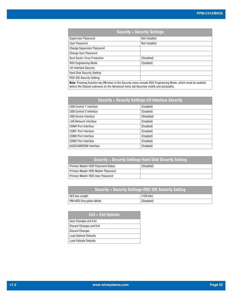
Security > Security SettingsSupervisor Password Not Installed
User Password Not Installed
Change Supervisor Password
Change User Password
Boot Sector Virus Protection [Disabled]
RDC Engineering Mode [Enabled]
I/O Interface Security
Hard Disk Security Setting
RDC IDE Security Setting
Note: Pressing function key F4 when in the Security menu reveals RDC Engineering Mode, which must be enabled before the Chipset submenu on the Advanced menu tab becomes visible and accessible.
Security > Security Settings-I/O Interface SecurityUSB Control 1 Interface [Enabled]
USB Control 2 Interface [Enabled]
USB Device Interface [Disabled]
LAN Network Interface [Enabled]
COM4 Port Interface [Enabled]
COM1 Port Interface [Enabled]
COM3 Port Interface [Enabled]
COM2 Port Interface [Enabled]
AUDIO/MODEM Interface [Enabled]
Security > Security Settings-Hard Disk Security SettingPrimary Master HDD Password Status [Disabled]
Primary Master HDD Master Password
Primary Master HDD User Password
Security > Security Settings-RDC IDE Security SettingAES key Length [128 bits]
PM-HDD Encryption Mode [Disabled]
Exit > Exit OptionsSave Changes and Exit
Discard Changes and Exit
Discard Changes
Load Optimal Defaults
Load Failsafe Defaults
www.winsystems.com Page 52
PPM-C412/Cables and Accessories
v1.0
8.5 BIOS Setting Storage Options
8.5.1 CMOS Storage Locations
The PPM-C412’s BIOS configuration is stored in two locations:
• CMOS RAM (nonvolatile if battery backed)
• FLASH PROM (nonvolatile storage for factory defaults)
8.5.2 Saving the CMOS Configuration
The real-time clock and the CMOS RAM settings can be maintained by an optional battery when the board is powered off. A battery is always required to maintain time and date functions when the board is powered off.
8.5.3 Updating the BIOS FLASH PROM
The most recent PPM-C412 BIOS is available on the WinSystems website at www.winsystems.com. However, it is highly recommended that an Applications Engineer be consulted prior to any BIOS FLASH ROM update.
9. Cables and AccessoriesWinSystems cables and batteries simplify connection to the PPM-C412. The following table contains a partial list of available items. For additional cables and accessories along with technical details, visit www.winsystems.com.
Table 20: Cable and battery specifications
Part Number Description
CBL-SET-412-1 Set of cables for the PPM-C412 CBL-SATA-701-20 SATA cableCBL-251-G-1-1.5 1-ft. multi-I/O cableCBL-174-G-1-1.5 18-in. 8-wire power cableCBL-234-G-1-1.375 1-ft VGA adapter cable
www.winsystems.com Page 53
PPM-C412/Software Drivers
v1.0
Standoff kits are available and recommended for use with the PPM-C412. The following table lists the items contained in each kit.
10. Software DriversGo to www.winsystems.com for information on available software drivers.
CBL-USB4-002-12 4x USB ports to two, 2-mm 2x4 connectorsADP-IO-USB-002 Dual 8-pin, 2-mm to 4x Type A USB connectorsCBL-ENET1-302-12 Gigabit Ethernet cableCBL-DIO24-001-12 Digital I/O adapter cable to Pico-ClaspCBL-DIO24-002-12 Digital I/O adapter cable to 0.1” centersCBL-LED3-000-14 Unterminated LED extension cableCBL-LED3-001-12 Same terminated LED extension cableCBL-SPL-001-14 LVDS and audio to unterminated LVDS with audio jacksBAT-LTC-E-36-16-1 External 3.6V, 1600 mAH battery with plug-in connector BAT-LTC-E-36-27-1 External 3.6V, 2700 mAH battery with plug-in connector
Table 20: Cable and battery specifications (Continued)
Part Number Description
Table 21: Standoff kits
Kit Component Description Qty
KIT-PCM-STANDOFF-44 pc. nylon hex PC/104 standoff kit
Standoff Nylon 0.25” hex, 0.600” long male/female 4-40 4Hex nut Hex nylon 4-40 4Screw Phillips-pan head (PPH) 4-40 x 1/4” stainless steel 4
KIT-PCM-STANDOFF-B-44 pc. brass hex PC/104 standoff kit
Standoff Brass 5 mm hex, 0.600” long male/female 4-40 4Hex nut 4-40 x 0.095 thick, nickel finish 4Screw Phillips-pan head (PPH) 4-40 x 1/4” stainless steel 4
www.winsystems.com Page 54
PPM-C412/Best Practices
v1.0
Appendix A. Best Practices
The following paragraphs outline the best practices for operating the PPM-C412 in a safe, effective manner, that does not damage the board. Please read this section carefully.
Power Supply
Power Supply Budget
Evaluate your power supply budget. It is usually good practice to budget twice the typical power requirement for all of your devices.
Zero-load Power Supply
Use a zero-load power supply whenever possible. A zero-load power supply does not require a minimum power load to regulate. If a zero-load power supply is not appropriate for your application, then verify that the single board computer’s typical load is not lower than the power supply’s minimum load. If the single board computer does not draw enough power to meet the power supply’s minimum load, then the power supply does not regulate properly and can cause damage to the PPM-C412.
Power Down
Make sure that power has been removed from the system before making or breaking any connections.
Avoid Electrostatic Discharge (ESD)—Only handle the circuit board and other bare electronics when electrostatic discharge (ESD) protection is in place. Having a wrist strap and a fully grounded workstation is the minimum ESD protection required before the ESD seal on the product bag is broken.
Use Proper Power Connections (Voltage)—When verifying the voltage, measure it at the power connector on the PPM-C412. Measuring it at the power supply does not account for voltage drop through the wire and connectors.
The PPM-C412 requires +5V (±5%) to operate. Verify the power connections. Incorrect voltages can cause catastrophic damage.
Populate all of the +5V and ground connections. Most single board computers have multiple power and ground pins, and all of them should be populated. The more copper connecting the power supply to the PPM-C412, the better.
Power Supply OFF—The power supply should always be off before it is connected to the I/O Module. Do not hot-plug the PPM-C412 on a host platform that is already powered.
www.winsystems.com Page 55
PPM-C412/Best Practices
v1.0
I/O Connections OFF—I/O Connections should also be off before connecting them to the embedded computer modules or any I/O cards. Connecting hot signals can cause damage whether the embedded system is powered or not.
Mounting and Protecting the I/O Module
The PPM-C412 must be mounted properly to avoid damage. Standoff kits are available and recommended for use with the PPM-C412. See Table 21 on page 54 for details.
Placing the PPM-C412 on Mounting Standoffs—Be careful when placing the PPM-C412 on the mounting standoffs. Sliding the board around until the standoffs are visible from the top can cause component damage on the bottom of the board.
Do Not Bend or Flex the PPM-C412—Bending or flexing can cause irreparable damage. Embedded computer modules are especially sensitive to flexing or bending around Ball Grid Array (BGA) devices. BGA devices are extremely rigid by design and flexing or bending the embedded computer module can cause the BGA to tear away from the printed circuit board.
Mounting Holes—The mounting holes are plated on the top, bottom and through the barrel of the hole and are connected to the embedded computer module’s ground plane. Traces are often routed in the inner layers right below, above or around the mounting holes.
• Never use a drill or any other tool in an attempt to make the holes larger.
• Never use screws with oversized heads. The head could come in contact with nearby components causing a short or physical damage.
• Never use self-tapping screws; they compromise the walls of the mounting hole.
• Never use oversized screws that cut into the walls of the mounting holes.
• Always use all of the mounting holes. By using all of the mounting holes, you pro-vide the support the embedded computer module needs to prevent bending or flex-ing.
Plug or Unplug Connectors Only on Fully Mounted Boards—Never plug or unplug connectors on a board that is not fully mounted. Many of the connectors fit rather tightly and the force needed to plug or unplug them could cause the embedded computer module to be flexed.
Avoid Cutting the PPM-C412—Never use star washers or any fastening hardware that cut into the PPM-C412.
Avoid Over-tightening of Mounting Hardware—Causing the area around the mounting holes to compress could damage interlayer traces around the mounting holes.
Use Appropriate Tools—Always use tools that are appropriate for working with small hardware. Large tools can damage components around the mounting holes.
www.winsystems.com Page 56
PPM-C412/Best Practices
v1.0
Avoid Conductive Surfaces—Never allow the embedded computer module to be placed on a conductive surface. Many embedded systems use a battery to back up the clock-calendar and CMOS memory. A conductive surface such as a metal bench can short the battery causing premature failure.
Adding PC/104 Boards to Your Stack
Be careful when adding PC/104 boards to your stack—Never allow the power to be turned on when a PC/104 board has been improperly plugged onto the stack. It is possible to misalign the PC/104 card and leave a row of pins on the end or down the long side hanging out of the connector. If power is applied with these pins misaligned, it causes the I/O board to be damaged beyond repair.
Conformal Coating
Applying conformal coating to a WinSystems product does not in itself void the product warranty, if it is properly removed prior to return. Coating may change thermal characteristics and impedes our ability to test, diagnose, and repair products. Any coated product sent to WinSystems for repair will be returned at customer expense and no service will be performed.
WinSystems offers conformal coating services. Please contact an Applications Engineer for details.
Operations/Product Manuals
Every single board computer has an Operations manual or Product manual.
Periodic Updates—Operations/Product manuals are updated often. Periodically check the WinSystems website (http://www.winsystems.com) for revisions.
Check Pinouts—Always check the pinout and connector locations in the manual before plugging in a cable. Many I/O modules have identical headers for different functions and plugging a cable into the wrong header can have disastrous results.
Contact an Applications Engineer—If a diagram or chart in a manual does not seem to match your board, or if you have additional questions, contact a WinSystems Applications Engineer at: +1-817-274-7553.
www.winsystems.com Page 57
PPM-C412/Mechanical Drawings
v1.0
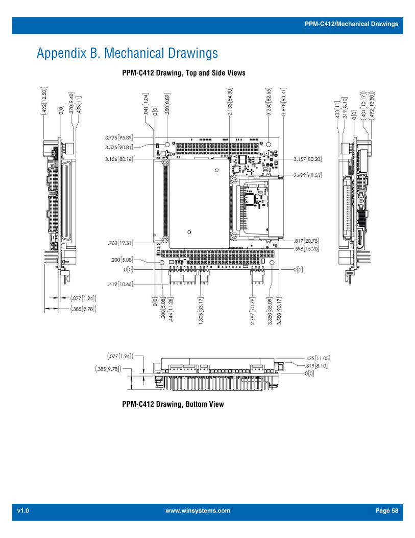
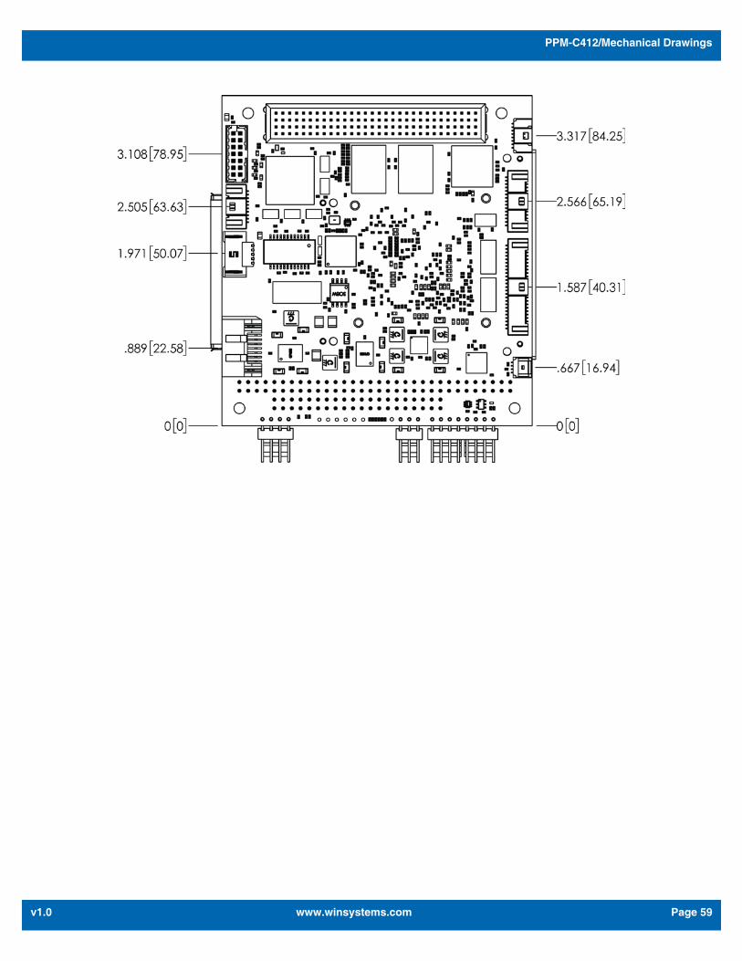
Appendix B. Mechanical DrawingsPPM-C412 Drawing, Top and Side Views
PPM-C412 Drawing, Bottom View
www.winsystems.com Page 58
PPM-C412/Mechanical Drawings
v1.0
www.winsystems.com Page 59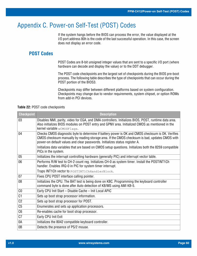
PPM-C412/Power-on Self-Test (POST) Codes
v1.0
Appendix C. Power-on Self-Test (POST) CodesIf the system hangs before the BIOS can process the error, the value displayed at the I/O port address 80h is the code of the last successful operation. In this case, the screen does not display an error code.
POST Codes
POST Codes are 8-bit unsigned integer values that are sent to a specific I/O port (where hardware can decode and display the value) or to the DDT debugger.
The POST code checkpoints are the largest set of checkpoints during the BIOS pre-boot process. The following table describes the type of checkpoints that can occur during the POST portion of the BIOS3.
Checkpoints may differ between different platforms based on system configuration. Checkpoints may change due to vendor requirements, system chipset, or option ROMs from add-in PCI devices.
Table 22: POST code checkpoints
Checkpoint Description
03 Disables NMI, parity, video for EGA, and DMA controllers. Initializes BIOS, POST, runtime data area. Also initializes BIOS modules on POST entry and GPNV area. Initialized CMOS as mentioned in the kernel variable wCMOSFlags.
04 Checks CMOS diagnostic byte to determine if battery power is OK and CMOS checksum is OK. Verifies CMOS checksum manually by reading storage area. If the CMOS checksum is bad, updates CMOS with power-on default values and clear passwords. Initializes status register A.Initializes data variables that are based on CMOS setup questions. Initializes both the 8259 compatible PICs in the system.
05 Initializes the interrupt controlling hardware (generally PIC) and interrupt vector table.06 Performs R/W test to CH-2 count reg. Initializes CH-0 as system timer. Install the POSTINT1Ch
handler. Enables IRQ-0 in PIC for system timer interrupt. Traps INT1Ch vector to POSTINT1ChHandlerBlock.
07 Fixes CPU POST interface calling pointer.08 Initializes the CPU. The BAT test is being done on KBC. Programming the keyboard controller
command byte is done after Auto detection of KB/MS using AMI KB-5.C0 Early CPU Init Start – Disable Cache – Init Local APICC1 Sets up boot strap processor information.C2 Sets up boot strap processor for POST.C5 Enumerates and sets up application processors.C6 Re-enables cache for boot strap processor.C7 Early CPU Init Exit0A Initializes the 8042 compatible keyboard controller.0B Detects the presence of PS/2 mouse.
www.winsystems.com Page 60
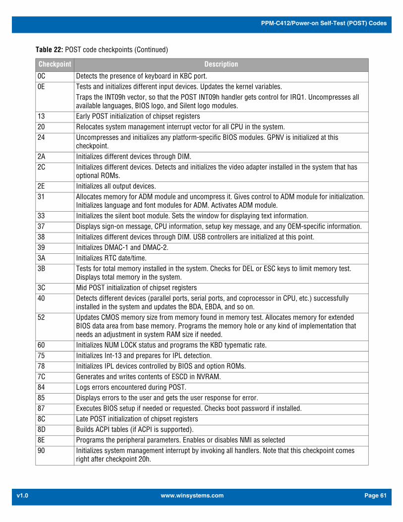
PPM-C412/Power-on Self-Test (POST) Codes
v1.0
0C Detects the presence of keyboard in KBC port.0E Tests and initializes different input devices. Updates the kernel variables.
Traps the INT09h vector, so that the POST INT09h handler gets control for IRQ1. Uncompresses all available languages, BIOS logo, and Silent logo modules.
13 Early POST initialization of chipset registers20 Relocates system management interrupt vector for all CPU in the system.24 Uncompresses and initializes any platform-specific BIOS modules. GPNV is initialized at this
checkpoint.2A Initializes different devices through DIM.2C Initializes different devices. Detects and initializes the video adapter installed in the system that has
optional ROMs.2E Initializes all output devices.31 Allocates memory for ADM module and uncompress it. Gives control to ADM module for initialization.
Initializes language and font modules for ADM. Activates ADM module.33 Initializes the silent boot module. Sets the window for displaying text information.37 Displays sign-on message, CPU information, setup key message, and any OEM-specific information.38 Initializes different devices through DIM. USB controllers are initialized at this point.39 Initializes DMAC-1 and DMAC-2.3A Initializes RTC date/time.3B Tests for total memory installed in the system. Checks for DEL or ESC keys to limit memory test.
Displays total memory in the system.3C Mid POST initialization of chipset registers40 Detects different devices (parallel ports, serial ports, and coprocessor in CPU, etc.) successfully
installed in the system and updates the BDA, EBDA, and so on.52 Updates CMOS memory size from memory found in memory test. Allocates memory for extended
BIOS data area from base memory. Programs the memory hole or any kind of implementation that needs an adjustment in system RAM size if needed.
60 Initializes NUM LOCK status and programs the KBD typematic rate.75 Initializes Int-13 and prepares for IPL detection.78 Initializes IPL devices controlled by BIOS and option ROMs.7C Generates and writes contents of ESCD in NVRAM.84 Logs errors encountered during POST.85 Displays errors to the user and gets the user response for error.87 Executes BIOS setup if needed or requested. Checks boot password if installed.8C Late POST initialization of chipset registers8D Builds ACPI tables (if ACPI is supported).8E Programs the peripheral parameters. Enables or disables NMI as selected90 Initializes system management interrupt by invoking all handlers. Note that this checkpoint comes
right after checkpoint 20h.
Table 22: POST code checkpoints (Continued)
Checkpoint Description
www.winsystems.com Page 61
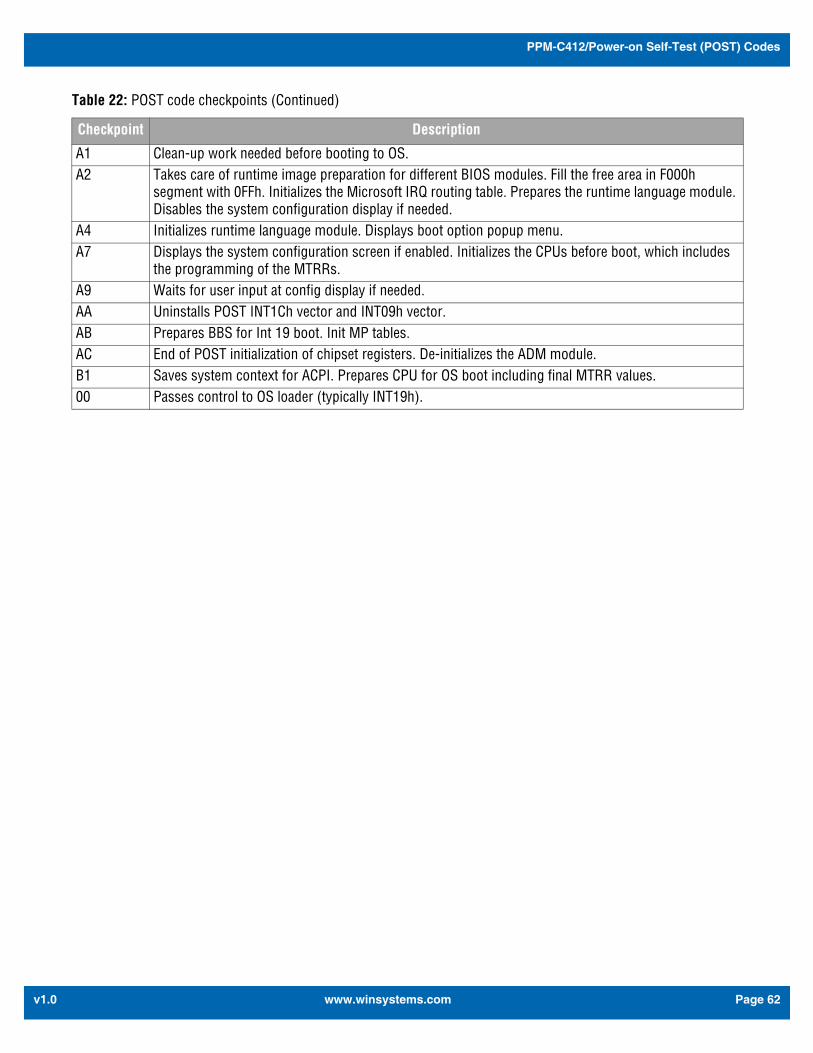
PPM-C412/Power-on Self-Test (POST) Codes
v1.0
A1 Clean-up work needed before booting to OS.A2 Takes care of runtime image preparation for different BIOS modules. Fill the free area in F000h
segment with 0FFh. Initializes the Microsoft IRQ routing table. Prepares the runtime language module. Disables the system configuration display if needed.
A4 Initializes runtime language module. Displays boot option popup menu.A7 Displays the system configuration screen if enabled. Initializes the CPUs before boot, which includes
the programming of the MTRRs.A9 Waits for user input at config display if needed.AA Uninstalls POST INT1Ch vector and INT09h vector.AB Prepares BBS for Int 19 boot. Init MP tables.AC End of POST initialization of chipset registers. De-initializes the ADM module.B1 Saves system context for ACPI. Prepares CPU for OS boot including final MTRR values.00 Passes control to OS loader (typically INT19h).
Table 22: POST code checkpoints (Continued)
Checkpoint Description
www.winsystems.com Page 62
PPM-C412/Warranty Information
v1.0
Appendix D. Warranty InformationWARRANTY
(http://www.winsystems.com/company/warranty.cfm)
WinSystems warrants to Customer that for a period of two (2) years from the date of shipment any Products and Software purchased or licensed hereunder which have been developed or manufactured by WinSystems shall be free of any material defects and shall perform substantially in accordance with WinSystems' specifications therefore. With respect to any Products or Software purchased or licensed hereunder which have been developed or manufactured by others, WinSystems shall transfer and assign to Customer any warranty
of such manufacturer or developer held by WinSystems, provided that the warranty, if any, may be assigned. Notwithstanding anything herein to the contrary, this warranty granted by WinSystems to the Customer shall be for the sole benefit of the Customer, and may not be assigned, transferred or conveyed to any third party. The sole obligation of WinSystems for any breach of warranty contained herein shall be, at its option, either (i) to repair or replace at its expense any materially defective Products or Software, or (ii) to take back such Products and Software and refund the Customer the purchase price and any license fees paid for the same. Customer shall pay all freight, duty, broker's fees, insurance charges for the return of any Products or Software to WinSystems under this warranty. WinSystems shall pay freight and insurance charges for any repaired or replaced Products or Software thereafter delivered to Customer within the United States. All fees and costs for shipment outside of the United States shall be paid by Customer. The foregoing warranty shall not apply to any Products of Software which have been subject to abuse, misuse, vandalism, accidents, alteration, neglect, unauthorized repair or improper installations.
THERE ARE NO WARRANTIES BY WINSYSTEMS EXCEPT AS STATED HEREIN, THERE ARE NO OTHER WARRANTIES EXPRESS OR IMPLIED INCLUDING, BUT NOT LIMITED TO, THE IMPLIED WARRANTIES OF MERCHANTABILITY AND FITNESS FOR A PARTICULAR PURPOSE, IN NO EVENT SHALL WINSYSTEMS BE LIABLE FOR CONSEQUENTIAL, INCIDENTIAL OR SPECIAL DAMAGES INCLUDING, BUT NOT LIMITED TO, DAMAGES FOR LOSS OF DATA, PROFITS OR GOODWILL. WINSYSTEMS' MAXIMUM LIABILITY FOR ANY BREACH OF THIS AGREEMENT OR OTHER CLAIM RELATED TO ANY PRODUCTS, SOFTWARE, OR THE SUBJECT MATTER HEREOF, SHALL NOT EXCEED THE PURCHASE PRICE OR LICENSE FEE PAID BY CUSTOMER TO WINSYSTEMS FOR THE PRODUCTS OR SOFTWARE OR PORTION THEREOF TO WHICH SUCH BREACH OR CLAIM PERTAINS.
Warranty Service
1. To obtain service under this warranty, obtain a return authorization number. In the United States, contact the WinSystems' Service Center for a return authorization number. Outside the United States, contact your local sales agent for a return authorization number.
2. You must send the product postage prepaid and insured. You must enclose the products in an anti-static bag to protect from damage by static electricity. WinSystems is not responsible for damage to the product due to static electricity.
www.winsystems.com Page 63