Zynq UltraScale+ MPSoC Packaging and Pinouts Product Specification User Guide UG1075 (v1.0.2) January 20, 2016

Welcome message from author
This document is posted to help you gain knowledge. Please leave a comment to let me know what you think about it! Share it to your friends and learn new things together.
Transcript
Zynq UltraScale+ MPSoC Packaging and Pinouts
Product Specification User Guide
UG1075 (v1.0.2) January 20, 2016
Zynq UltraScale+ Packaging and Pinouts www.xilinx.com 2UG1075 (v1.0.2) January 20, 2016
Revision HistoryThe following table shows the revision history for this document.
Date Version Revision
01/20/2016 1.0.2 Replaced the missing graphics in Chapter 1.
12/18/2015 1.0.1 Updated the package file links in Chapter 2.
11/24/2015 1.0 Initial Xilinx release.
Send Feedback
Table of ContentsRevision History . . . . . . . . . . . . . . . . . . . . . . . . . . . . . . . . . . . . . . . . . . . . . . . . . . . . . . . . . . . . . . . . . . . . 2
Chapter 1: Packaging OverviewIntroduction to the UltraScale Architecture . . . . . . . . . . . . . . . . . . . . . . . . . . . . . . . . . . . . . . . . . . . . 5Zynq UltraScale+ MPSoC Packaging and Pinouts. . . . . . . . . . . . . . . . . . . . . . . . . . . . . . . . . . . . . . . . . 6Differences from Previous Generations . . . . . . . . . . . . . . . . . . . . . . . . . . . . . . . . . . . . . . . . . . . . . . . . 6Device/Package Combinations . . . . . . . . . . . . . . . . . . . . . . . . . . . . . . . . . . . . . . . . . . . . . . . . . . . . . . . 7Gigabit Transceiver Channels by Device/Package . . . . . . . . . . . . . . . . . . . . . . . . . . . . . . . . . . . . . . . . 7User I/O Pins by Device/Package . . . . . . . . . . . . . . . . . . . . . . . . . . . . . . . . . . . . . . . . . . . . . . . . . . . . . 9Pin Definitions . . . . . . . . . . . . . . . . . . . . . . . . . . . . . . . . . . . . . . . . . . . . . . . . . . . . . . . . . . . . . . . . . . . 10Footprint Compatibility between Packages . . . . . . . . . . . . . . . . . . . . . . . . . . . . . . . . . . . . . . . . . . . . 16Die Level Bank Numbering Overview . . . . . . . . . . . . . . . . . . . . . . . . . . . . . . . . . . . . . . . . . . . . . . . . . 22
Chapter 2: Package FilesAbout ASCII Package Files . . . . . . . . . . . . . . . . . . . . . . . . . . . . . . . . . . . . . . . . . . . . . . . . . . . . . . . . . . 46ASCII Pinout Files . . . . . . . . . . . . . . . . . . . . . . . . . . . . . . . . . . . . . . . . . . . . . . . . . . . . . . . . . . . . . . . . . 47
Chapter 3: Device DiagramsSummary. . . . . . . . . . . . . . . . . . . . . . . . . . . . . . . . . . . . . . . . . . . . . . . . . . . . . . . . . . . . . . . . . . . . . . . . 48SBVA484 Package–XCZU2EG and XCZU3EG . . . . . . . . . . . . . . . . . . . . . . . . . . . . . . . . . . . . . . . . . . . . 49SFVA625 Package–XCZU2EG and XCZU3EG . . . . . . . . . . . . . . . . . . . . . . . . . . . . . . . . . . . . . . . . . . . . 51SFVC784 Package–XCZU2EG and XCZU3EG . . . . . . . . . . . . . . . . . . . . . . . . . . . . . . . . . . . . . . . . . . . . 53FFVC900 Package–XCZU6EG and XCZU9EG . . . . . . . . . . . . . . . . . . . . . . . . . . . . . . . . . . . . . . . . . . . . 55FFVB1156 Package–XCZU6EG and XCZU9EG . . . . . . . . . . . . . . . . . . . . . . . . . . . . . . . . . . . . . . . . . . . 57FBVB900 Package–XCZU15EG . . . . . . . . . . . . . . . . . . . . . . . . . . . . . . . . . . . . . . . . . . . . . . . . . . . . . . . 59FFVB1156 Package–XCZU15EG . . . . . . . . . . . . . . . . . . . . . . . . . . . . . . . . . . . . . . . . . . . . . . . . . . . . . . 61
Chapter 4: Mechanical DrawingsSummary. . . . . . . . . . . . . . . . . . . . . . . . . . . . . . . . . . . . . . . . . . . . . . . . . . . . . . . . . . . . . . . . . . . . . . . . 63FFVC900 Flip-Chip, Fine-Pitch BGA
(XCZU6EG, XCZU9EG, and XCZU15EG) . . . . . . . . . . . . . . . . . . . . . . . . . . . . . . . . . . . . . . . . . . . . . 64FFVB1156 Flip-Chip, Fine-Pitch BGA
(XCZU6EG, XCZU9EG, and XCZU15EG) . . . . . . . . . . . . . . . . . . . . . . . . . . . . . . . . . . . . . . . . . . . . . 65
Zynq UltraScale+ Packaging and Pinouts www.xilinx.com 3UG1075 (v1.0.2) January 20, 2016
Send Feedback
Chapter 5: Package MarkingIntroduction . . . . . . . . . . . . . . . . . . . . . . . . . . . . . . . . . . . . . . . . . . . . . . . . . . . . . . . . . . . . . . . . . . . . . 66
Chapter 6: Packing and ShippingIntroduction . . . . . . . . . . . . . . . . . . . . . . . . . . . . . . . . . . . . . . . . . . . . . . . . . . . . . . . . . . . . . . . . . . . . . 68
Chapter 7: Soldering GuidelinesSoldering Guidelines . . . . . . . . . . . . . . . . . . . . . . . . . . . . . . . . . . . . . . . . . . . . . . . . . . . . . . . . . . . . . . 69
Chapter 8: Recommended PCB Design Rules for BGA PackagesBGA Packages . . . . . . . . . . . . . . . . . . . . . . . . . . . . . . . . . . . . . . . . . . . . . . . . . . . . . . . . . . . . . . . . . . . . 73
Chapter 9: Thermal SpecificationsIntroduction . . . . . . . . . . . . . . . . . . . . . . . . . . . . . . . . . . . . . . . . . . . . . . . . . . . . . . . . . . . . . . . . . . . . . 75Thermal Resistance Data . . . . . . . . . . . . . . . . . . . . . . . . . . . . . . . . . . . . . . . . . . . . . . . . . . . . . . . . . . . 75Support for Thermal Models . . . . . . . . . . . . . . . . . . . . . . . . . . . . . . . . . . . . . . . . . . . . . . . . . . . . . . . . 77
Chapter 10: Thermal Management StrategyIntroduction . . . . . . . . . . . . . . . . . . . . . . . . . . . . . . . . . . . . . . . . . . . . . . . . . . . . . . . . . . . . . . . . . . . . . 78Thermal Interface Material . . . . . . . . . . . . . . . . . . . . . . . . . . . . . . . . . . . . . . . . . . . . . . . . . . . . . . . . . 79Heat Sink Removal Procedure. . . . . . . . . . . . . . . . . . . . . . . . . . . . . . . . . . . . . . . . . . . . . . . . . . . . . . . 82
Chapter 11: Heat Sink Guidelines for Lidless Flip-Chip PackagesHeat Sink Attachments for Lidless FB Packages. . . . . . . . . . . . . . . . . . . . . . . . . . . . . . . . . . . . . . . . . 83Types of Heat Sink Attachments . . . . . . . . . . . . . . . . . . . . . . . . . . . . . . . . . . . . . . . . . . . . . . . . . . . . . 84
Appendix A: Additional Resources and Legal NoticesXilinx Resources . . . . . . . . . . . . . . . . . . . . . . . . . . . . . . . . . . . . . . . . . . . . . . . . . . . . . . . . . . . . . . . . . . 89Solution Centers. . . . . . . . . . . . . . . . . . . . . . . . . . . . . . . . . . . . . . . . . . . . . . . . . . . . . . . . . . . . . . . . . . 89References . . . . . . . . . . . . . . . . . . . . . . . . . . . . . . . . . . . . . . . . . . . . . . . . . . . . . . . . . . . . . . . . . . . . . . 89Please Read: Important Legal Notices . . . . . . . . . . . . . . . . . . . . . . . . . . . . . . . . . . . . . . . . . . . . . . . . 91
Zynq UltraScale+ Packaging and Pinouts www.xilinx.com 4UG1075 (v1.0.2) January 20, 2016
Send Feedback
Chapter 1
Packaging Overview
Introduction to the UltraScale ArchitectureThe Xilinx® UltraScale™ architecture is the first ASIC-class All Programmable architecture to enable multi-hundred gigabit-per-second levels of system performance with smart processing, while efficiently routing and processing data on-chip. UltraScale architecture-based devices address a vast spectrum of high-bandwidth, high-utilization system requirements by using industry-leading technical innovations, including next-generation routing, ASIC-like clocking, 3D-on-3D ICs, multiprocessor SoC (MPSoC) technologies, and new power reduction features. The devices share many building blocks, providing scalability across process nodes and product families to leverage system-level investment across platforms.
Virtex® UltraScale+™ devices provide the highest performance and integration capabilities in a FinFET node, including both the highest serial I/O and signal processing bandwidth, as well as the highest on-chip memory density. As the industry's most capable FPGA family, the Virtex UltraScale+ devices are ideal for applications including 1+Tb/s networking and data center and fully integrated radar/early-warning systems.
Virtex UltraScale devices provide the greatest performance and integration at 20 nm, including serial I/O bandwidth and logic capacity. As the industry's only high-end FPGA at the 20 nm process node, this family is ideal for applications including 400G networking, large scale ASIC prototyping, and emulation.
Kintex® UltraScale+ devices provide the best price/performance/watt balance in a FinFET node, delivering the most cost-effective solution for high-end capabilities, including transceiver and memory interface line rates as well as 100G connectivity cores. Our newest mid-range family is ideal for both packet processing and DSP-intensive functions and is well suited for applications including wireless MIMO technology, Nx100G networking, and data center.
Kintex UltraScale devices provide the best price/performance/watt at 20 nm and include the highest signal processing bandwidth in a mid-range device, next-generation transceivers, and low-cost packaging for an optimum blend of capability and cost-effectiveness. The family is ideal for packet processing in 100G networking and data centers applications as well as DSP-intensive processing needed in next-generation medical imaging, 8k4k video, and heterogeneous wireless infrastructure.
Zynq UltraScale+ Packaging and Pinouts www.xilinx.com 5UG1075 (v1.0.2) January 20, 2016
Send Feedback
Chapter 1: Packaging Overview
Zynq® UltraScale+ MPSoC devices provide 64-bit processor scalability while combining real-time control with soft and hard engines for graphics, video, waveform, and packet processing. Integrating an ARM®-based system for advanced analytics and on-chip programmable logic for task acceleration creates unlimited possibilities for applications including 5G Wireless, next generation ADAS, and Industrial Internet-of-Things.
This user guide is part of the Zynq UltraScale+ MPSoC documentation suite.
Zynq UltraScale+ MPSoC Packaging and PinoutsThis section describes the packages and pinouts for the in various organic flip-chip 0.8 mm and 1.0 mm pitch BGA packages.
IMPORTANT: All standard packages are lead-free (signified by an additional V in the package name). All devices supported in a particular package are footprint compatible. Each device is split into I/O banks to allow for flexibility in the choice of I/O standards. See the UltraScale Architecture SelectIO Resources User Guide (UG571) [Ref 3].
The flip-chip assembly materials for the Zynq UltraScale+ MPSoCs are manufactured using ultra-low alpha (ULA) materials defined as <0.002 cph/cm2 or materials that emit less than 0.002 alpha-particles per square centimeter per hour.
Differences from Previous GenerationsThe packaging and pinout specifications for Zynq UltraScale+ MPSoCs differ from past generations, including the Zynq-7000 AP SoCs. These details are outlined in this section.
• All package and die components, including flip-chip solder bumps, are lead-free.
• Package names contain a single-character alphabetic designator followed by the exact number of pins found on the package.
• VCCAUX_IO pins are not divided into bank groups. VCCAUX_IO must be connected to VCCAUX at the board level.
• Internal logic is separated from I/O logic by the addition of the VCCINT_IO power pins. VCCINT_IO must be connected to VCCBRAM (depending on the device speed grade and voltage settings) at the board level.
• Groups of gigabit serial transceiver (GT) power pins are separated by column for each column of GT Quads.
• Standard HP I/O banks each have a total of 52 SelectIO™ pins, optionally configurable as (up to) 24 differential pairs.
Zynq UltraScale+ Packaging and Pinouts www.xilinx.com 6UG1075 (v1.0.2) January 20, 2016
Send Feedback
Chapter 1: Packaging Overview
• Standard HD I/O banks each have a total of 24 SelectIO pins, optionally configurable as (up to) 12 differential pairs.
• Each bank has one dedicated VREF pin. These pins cannot be used as user I/Os.
• Four differential clock pin pairs per bank consist of a single type of global clock (GC or HDGC) input.
• Four memory byte groups per HP I/O bank are each separated into an upper and a lower memory byte group.
• Multiple PL configuration pins are removed.
• A POR_OVERRIDE pin is used to override the default power-on-reset delay. See Table 1-4.
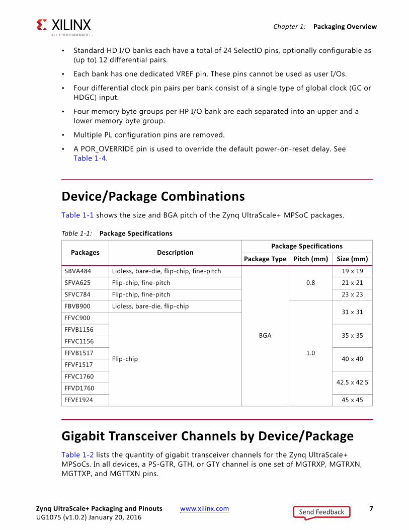
Device/Package CombinationsTable 1-1 shows the size and BGA pitch of the Zynq UltraScale+ MPSoC packages.
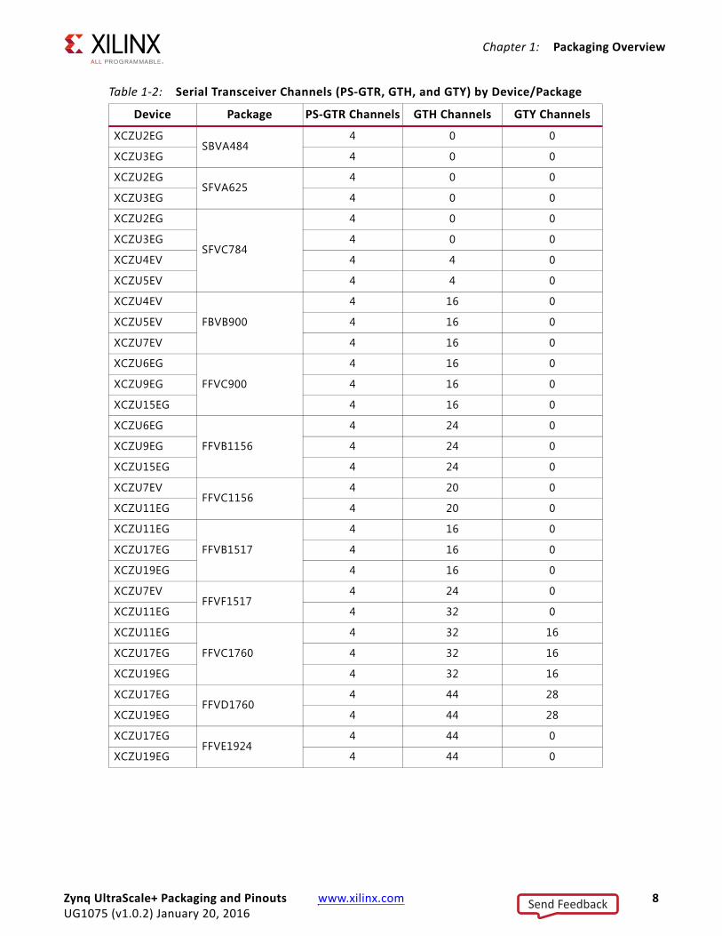
Gigabit Transceiver Channels by Device/PackageTable 1-2 lists the quantity of gigabit transceiver channels for the Zynq UltraScale+ MPSoCs. In all devices, a PS-GTR, GTH, or GTY channel is one set of MGTRXP, MGTRXN, MGTTXP, and MGTTXN pins.
Table 1-1: Package Specifications
Packages DescriptionPackage Specifications
Package Type Pitch (mm) Size (mm)
SBVA484 Lidless, bare-die, flip-chip, fine-pitch
BGA
0.8
19 x 19
SFVA625 Flip-chip, fine-pitch 21 x 21
SFVC784 Flip-chip, fine-pitch 23 x 23
FBVB900 Lidless, bare-die, flip-chip
1.0
31 x 31FFVC900
Flip-chip
FFVB115635 x 35
FFVC1156
FFVB151740 x 40
FFVF1517
FFVC176042.5 x 42.5
FFVD1760
FFVE1924 45 x 45
Zynq UltraScale+ Packaging and Pinouts www.xilinx.com 7UG1075 (v1.0.2) January 20, 2016
Send Feedback
Chapter 1: Packaging Overview
Table 1-2: Serial Transceiver Channels (PS-GTR, GTH, and GTY) by Device/Package
Device Package PS-GTR Channels GTH Channels GTY Channels
XCZU2EGSBVA484
4 0 0
XCZU3EG 4 0 0
XCZU2EGSFVA625
4 0 0
XCZU3EG 4 0 0
XCZU2EG
SFVC784
4 0 0
XCZU3EG 4 0 0
XCZU4EV 4 4 0
XCZU5EV 4 4 0
XCZU4EV
FBVB900
4 16 0
XCZU5EV 4 16 0
XCZU7EV 4 16 0
XCZU6EG
FFVC900
4 16 0
XCZU9EG 4 16 0
XCZU15EG 4 16 0
XCZU6EG
FFVB1156
4 24 0
XCZU9EG 4 24 0
XCZU15EG 4 24 0
XCZU7EVFFVC1156
4 20 0
XCZU11EG 4 20 0
XCZU11EG
FFVB1517
4 16 0
XCZU17EG 4 16 0
XCZU19EG 4 16 0
XCZU7EVFFVF1517
4 24 0
XCZU11EG 4 32 0
XCZU11EG
FFVC1760
4 32 16
XCZU17EG 4 32 16
XCZU19EG 4 32 16
XCZU17EGFFVD1760
4 44 28
XCZU19EG 4 44 28
XCZU17EGFFVE1924
4 44 0
XCZU19EG 4 44 0
Zynq UltraScale+ Packaging and Pinouts www.xilinx.com 8UG1075 (v1.0.2) January 20, 2016
Send Feedback
Chapter 1: Packaging Overview
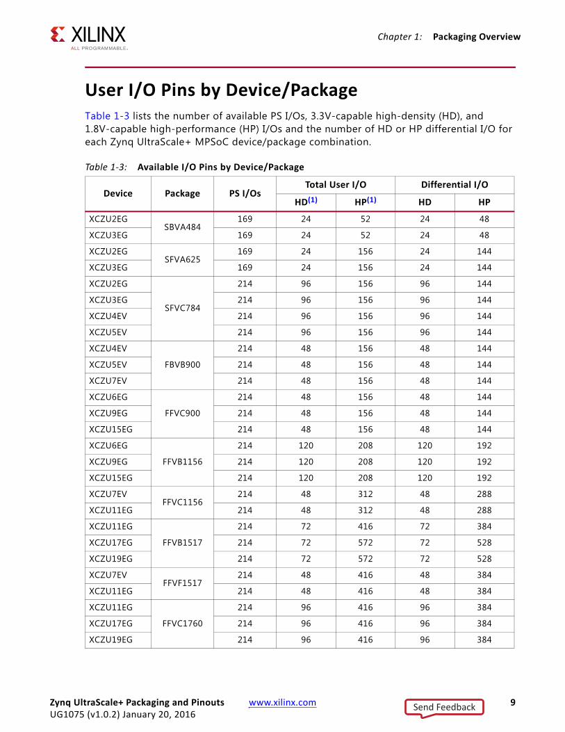
User I/O Pins by Device/PackageTable 1-3 lists the number of available PS I/Os, 3.3V-capable high-density (HD), and 1.8V-capable high-performance (HP) I/Os and the number of HD or HP differential I/O for each Zynq UltraScale+ MPSoC device/package combination.
Table 1-3: Available I/O Pins by Device/Package
Device Package PS I/OsTotal User I/O Differential I/O
HD(1) HP(1) HD HP
XCZU2EGSBVA484
169 24 52 24 48
XCZU3EG 169 24 52 24 48
XCZU2EGSFVA625
169 24 156 24 144
XCZU3EG 169 24 156 24 144
XCZU2EG
SFVC784
214 96 156 96 144
XCZU3EG 214 96 156 96 144
XCZU4EV 214 96 156 96 144
XCZU5EV 214 96 156 96 144
XCZU4EV
FBVB900
214 48 156 48 144
XCZU5EV 214 48 156 48 144
XCZU7EV 214 48 156 48 144
XCZU6EG
FFVC900
214 48 156 48 144
XCZU9EG 214 48 156 48 144
XCZU15EG 214 48 156 48 144
XCZU6EG
FFVB1156
214 120 208 120 192
XCZU9EG 214 120 208 120 192
XCZU15EG 214 120 208 120 192
XCZU7EVFFVC1156
214 48 312 48 288
XCZU11EG 214 48 312 48 288
XCZU11EG
FFVB1517
214 72 416 72 384
XCZU17EG 214 72 572 72 528
XCZU19EG 214 72 572 72 528
XCZU7EVFFVF1517
214 48 416 48 384
XCZU11EG 214 48 416 48 384
XCZU11EG
FFVC1760
214 96 416 96 384
XCZU17EG 214 96 416 96 384
XCZU19EG 214 96 416 96 384
Zynq UltraScale+ Packaging and Pinouts www.xilinx.com 9UG1075 (v1.0.2) January 20, 2016
Send Feedback
Chapter 1: Packaging Overview
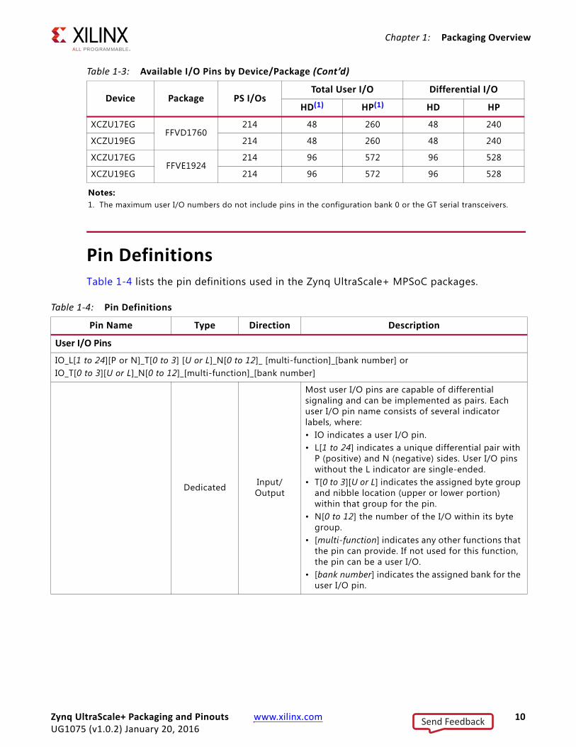
Pin DefinitionsTable 1-4 lists the pin definitions used in the Zynq UltraScale+ MPSoC packages.
XCZU17EGFFVD1760
214 48 260 48 240
XCZU19EG 214 48 260 48 240
XCZU17EGFFVE1924
214 96 572 96 528
XCZU19EG 214 96 572 96 528
Notes: 1. The maximum user I/O numbers do not include pins in the configuration bank 0 or the GT serial transceivers.
Table 1-3: Available I/O Pins by Device/Package (Cont’d)
Device Package PS I/OsTotal User I/O Differential I/O
HD(1) HP(1) HD HP
Table 1-4: Pin Definitions
Pin Name Type Direction Description
User I/O Pins
IO_L[1 to 24][P or N]_T[0 to 3] [U or L]_N[0 to 12]_ [multi-function]_[bank number] orIO_T[0 to 3][U or L]_N[0 to 12]_[multi-function]_[bank number]
Dedicated Input/Output
Most user I/O pins are capable of differential signaling and can be implemented as pairs. Each user I/O pin name consists of several indicator labels, where:• IO indicates a user I/O pin.• L[1 to 24] indicates a unique differential pair with
P (positive) and N (negative) sides. User I/O pins without the L indicator are single-ended.
• T[0 to 3][U or L] indicates the assigned byte group and nibble location (upper or lower portion) within that group for the pin.
• N[0 to 12] the number of the I/O within its byte group.
• [multi-function] indicates any other functions that the pin can provide. If not used for this function, the pin can be a user I/O.
• [bank number] indicates the assigned bank for the user I/O pin.
Zynq UltraScale+ Packaging and Pinouts www.xilinx.com 10UG1075 (v1.0.2) January 20, 2016
Send Feedback
Chapter 1: Packaging Overview
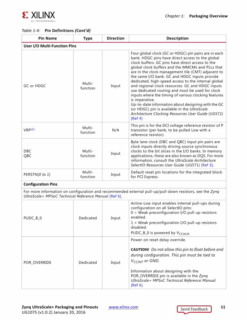
User I/O Multi-Function Pins
GC or HDGC Multi-function Input
Four global clock (GC or HDGC) pin pairs are in each bank. HDGC pins have direct access to the global clock buffers. GC pins have direct access to the global clock buffers and the MMCMs and PLLs that are in the clock management tile (CMT) adjacent to the same I/O bank. GC and HDGC inputs provide dedicated, high-speed access to the internal global and regional clock resources. GC and HDGC inputs use dedicated routing and must be used for clock inputs where the timing of various clocking features is imperative.Up-to-date information about designing with the GC (or HDGC) pin is available in the UltraScale Architecture Clocking Resources User Guide (UG572) [Ref 4]
VRP(1) Multi-function N/A
This pin is for the DCI voltage reference resistor of P transistor (per bank, to be pulled Low with a reference resistor).
DBCQBC
Multi-function Input
Byte lane clock (DBC and QBC) input pin pairs are clock inputs directly driving source synchronous clocks to the bit slices in the I/O banks. In memory applications, these are also known as DQS. For more information, consult the UltraScale Architecture SelectIO Resources User Guide (UG571) [Ref 3].
PERSTN[0 to 1] Multi-function Input Default reset pin locations for the integrated block
for PCI Express.
Configuration Pins
For more information on configuration and recommended external pull-up/pull-down resistors, see the Zynq UltraScale+ MPSoC Technical Reference Manual [Ref 6].
PUDC_B_0 Dedicated Input
Active-Low input enables internal pull-ups during configuration on all SelectIO pins: 0 = Weak preconfiguration I/O pull-up resistors enabled.1 = Weak preconfiguration I/O pull-up resistors disabled.PUDC_B_0 is powered by VCCAUX.
POR_OVERRIDE Dedicated Input
Power-on reset delay override.
CAUTION! Do not allow this pin to float before and during configuration. This pin must be tied to VCCINT or GND.
Information about designing with the POR_OVERRIDE pin is available in the Zynq UltraScale+ MPSoC Technical Reference Manual [Ref 6].
Table 1-4: Pin Definitions (Cont’d)
Pin Name Type Direction Description
Zynq UltraScale+ Packaging and Pinouts www.xilinx.com 11UG1075 (v1.0.2) January 20, 2016
Send Feedback
Chapter 1: Packaging Overview
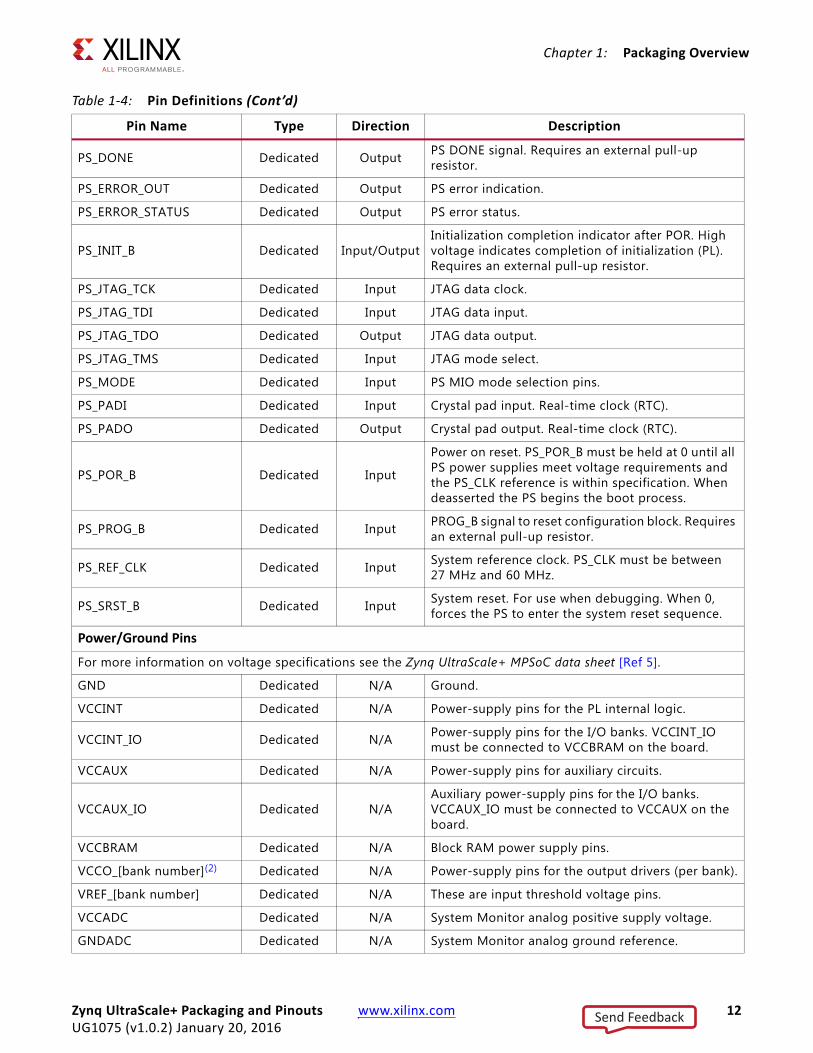
PS_DONE Dedicated Output PS DONE signal. Requires an external pull-up resistor.
PS_ERROR_OUT Dedicated Output PS error indication.
PS_ERROR_STATUS Dedicated Output PS error status.
PS_INIT_B Dedicated Input/OutputInitialization completion indicator after POR. High voltage indicates completion of initialization (PL). Requires an external pull-up resistor.
PS_JTAG_TCK Dedicated Input JTAG data clock.
PS_JTAG_TDI Dedicated Input JTAG data input.
PS_JTAG_TDO Dedicated Output JTAG data output.
PS_JTAG_TMS Dedicated Input JTAG mode select.
PS_MODE Dedicated Input PS MIO mode selection pins.
PS_PADI Dedicated Input Crystal pad input. Real-time clock (RTC).
PS_PADO Dedicated Output Crystal pad output. Real-time clock (RTC).
PS_POR_B Dedicated Input
Power on reset. PS_POR_B must be held at 0 until all PS power supplies meet voltage requirements and the PS_CLK reference is within specification. When deasserted the PS begins the boot process.
PS_PROG_B Dedicated Input PROG_B signal to reset configuration block. Requires an external pull-up resistor.
PS_REF_CLK Dedicated Input System reference clock. PS_CLK must be between 27 MHz and 60 MHz.
PS_SRST_B Dedicated Input System reset. For use when debugging. When 0, forces the PS to enter the system reset sequence.
Power/Ground Pins
For more information on voltage specifications see the Zynq UltraScale+ MPSoC data sheet [Ref 5].
GND Dedicated N/A Ground.
VCCINT Dedicated N/A Power-supply pins for the PL internal logic.
VCCINT_IO Dedicated N/A Power-supply pins for the I/O banks. VCCINT_IO must be connected to VCCBRAM on the board.
VCCAUX Dedicated N/A Power-supply pins for auxiliary circuits.
VCCAUX_IO Dedicated N/AAuxiliary power-supply pins for the I/O banks. VCCAUX_IO must be connected to VCCAUX on the board.
VCCBRAM Dedicated N/A Block RAM power supply pins.
VCCO_[bank number](2) Dedicated N/A Power-supply pins for the output drivers (per bank).
VREF_[bank number] Dedicated N/A These are input threshold voltage pins.
VCCADC Dedicated N/A System Monitor analog positive supply voltage.
GNDADC Dedicated N/A System Monitor analog ground reference.
Table 1-4: Pin Definitions (Cont’d)
Pin Name Type Direction Description
Zynq UltraScale+ Packaging and Pinouts www.xilinx.com 12UG1075 (v1.0.2) January 20, 2016
Send Feedback
Chapter 1: Packaging Overview
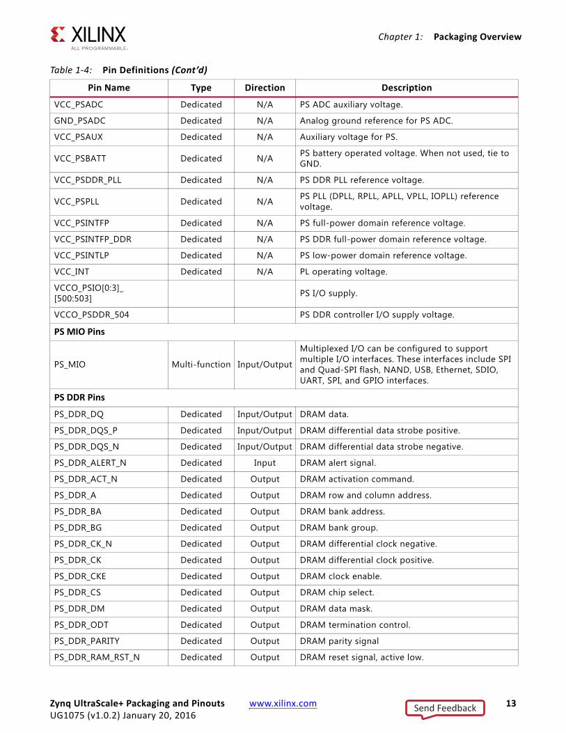
VCC_PSADC Dedicated N/A PS ADC auxiliary voltage.
GND_PSADC Dedicated N/A Analog ground reference for PS ADC.
VCC_PSAUX Dedicated N/A Auxiliary voltage for PS.
VCC_PSBATT Dedicated N/A PS battery operated voltage. When not used, tie to GND.
VCC_PSDDR_PLL Dedicated N/A PS DDR PLL reference voltage.
VCC_PSPLL Dedicated N/A PS PLL (DPLL, RPLL, APLL, VPLL, IOPLL) reference voltage.
VCC_PSINTFP Dedicated N/A PS full-power domain reference voltage.
VCC_PSINTFP_DDR Dedicated N/A PS DDR full-power domain reference voltage.
VCC_PSINTLP Dedicated N/A PS low-power domain reference voltage.
VCC_INT Dedicated N/A PL operating voltage.
VCCO_PSIO[0:3]_[500:503] PS I/O supply.
VCCO_PSDDR_504 PS DDR controller I/O supply voltage.
PS MIO Pins
PS_MIO Multi-function Input/Output
Multiplexed I/O can be configured to support multiple I/O interfaces. These interfaces include SPI and Quad-SPI flash, NAND, USB, Ethernet, SDIO, UART, SPI, and GPIO interfaces.
PS DDR Pins
PS_DDR_DQ Dedicated Input/Output DRAM data.
PS_DDR_DQS_P Dedicated Input/Output DRAM differential data strobe positive.
PS_DDR_DQS_N Dedicated Input/Output DRAM differential data strobe negative.
PS_DDR_ALERT_N Dedicated Input DRAM alert signal.
PS_DDR_ACT_N Dedicated Output DRAM activation command.
PS_DDR_A Dedicated Output DRAM row and column address.
PS_DDR_BA Dedicated Output DRAM bank address.
PS_DDR_BG Dedicated Output DRAM bank group.
PS_DDR_CK_N Dedicated Output DRAM differential clock negative.
PS_DDR_CK Dedicated Output DRAM differential clock positive.
PS_DDR_CKE Dedicated Output DRAM clock enable.
PS_DDR_CS Dedicated Output DRAM chip select.
PS_DDR_DM Dedicated Output DRAM data mask.
PS_DDR_ODT Dedicated Output DRAM termination control.
PS_DDR_PARITY Dedicated Output DRAM parity signal
PS_DDR_RAM_RST_N Dedicated Output DRAM reset signal, active low.
Table 1-4: Pin Definitions (Cont’d)
Pin Name Type Direction Description
Zynq UltraScale+ Packaging and Pinouts www.xilinx.com 13UG1075 (v1.0.2) January 20, 2016
Send Feedback
Chapter 1: Packaging Overview
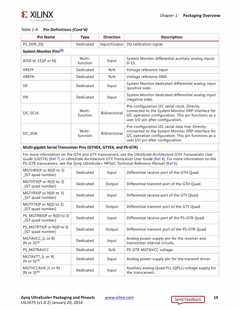
PS_DDR_ZQ Dedicated Input/Output ZQ calibration signal.
System Monitor Pins(3)
AD[0 to 15][P or N] Multi-function Input System Monitor differential auxiliary analog inputs
0–15.
VREFP Dedicated N/A Voltage reference input.
VREFN Dedicated N/A Voltage reference GND.
VP Dedicated Input System Monitor dedicated differential analog input (positive side).
VN Dedicated Input System Monitor dedicated differential analog input (negative side).
I2C_SCLK Multi-function Bidirectional
Pre-configuration I2C serial clock. Directly connected to the System Monitor DRP interface for I2C operation configuration. This pin functions as a user I/O pin after configuration.
I2C_SDA Multi-function Bidirectional
Pre-configuration I2C serial data line. Directly connected to the System Monitor DRP interface for I2C operation configuration. This pin functions as a user I/O pin after configuration.
Multi-gigabit Serial Transceiver Pins (GTHE4, GTYE4, and PS-GTR)
For more information on the GTH and GTY transceivers, see the UltraScale Architecture GTH Transceivers User Guide (UG576) [Ref 7] or UltraScale Architecture GTY Transceiver User Guide [Ref 8]. For more information on the PS-GTR transceivers, see the Zynq UltraScale+ MPSoC Technical Reference Manual [Ref 6].
MGTHRX[P or N][0 to 3]_[GT quad number] Dedicated Input Differential receive port of the GTH Quad.
MGTHTX[P or N][0 to 3]_[GT quad number] Dedicated Output Differential transmit port of the GTH Quad.
MGTYRX[P or N][0 to 3]_[GT quad number] Dedicated Input Differential receive port of the GTY Quad.
MGTYTX[P or N][0 to 3]_[GT quad number] Dedicated Output Differential transmit port of the GTY Quad.
PS_MGTRRX[P or N][0 to 3]_[GT quad number] Dedicated Input Differential receive port of the PS-GTR Quad.
PS_MGTRTX[P or N][0 to 3] _[GT quad number] Dedicated Output Differential transmit port of the PS-GTR Quad.
MGTAVCC_[L or R][N or S](4) Dedicated Input Analog power-supply pin for the receiver and
transmitter internal circuits.
PS_MGTRAVCC Dedicated N/A PS-GTR MGTAVCC voltage.
MGTAVTT_[L or R][N or S](4) Dedicated Input Analog power-supply pin for the transmit driver.
MGTVCCAUX_[L or R][N or S](4) Dedicated Input Auxiliary analog Quad PLL (QPLL) voltage supply for
the transceivers.
Table 1-4: Pin Definitions (Cont’d)
Pin Name Type Direction Description
Zynq UltraScale+ Packaging and Pinouts www.xilinx.com 14UG1075 (v1.0.2) January 20, 2016
Send Feedback
Chapter 1: Packaging Overview
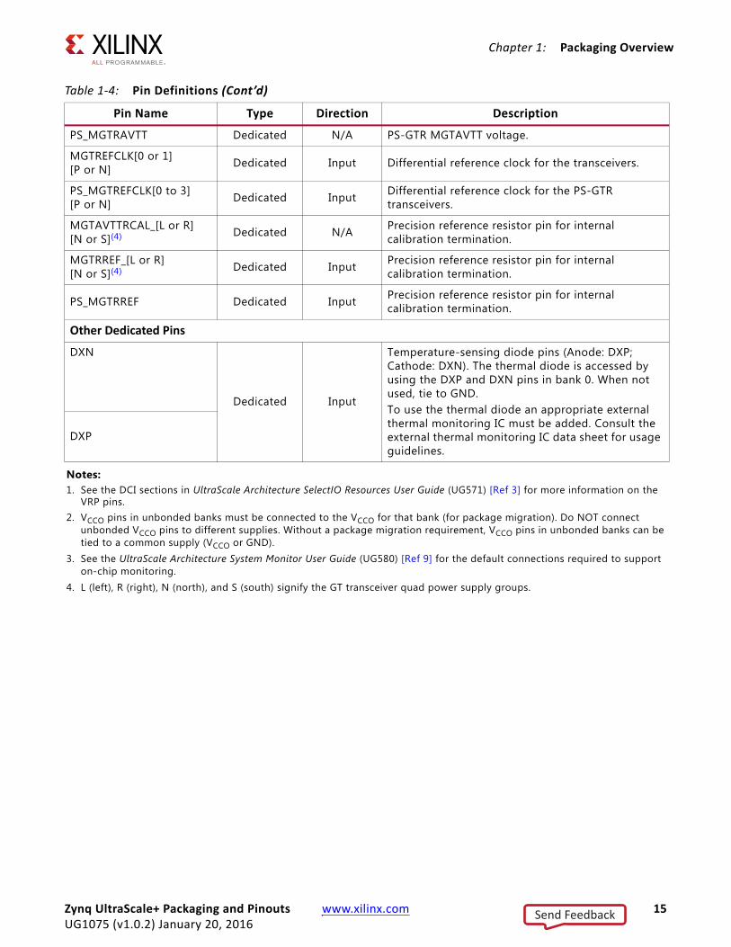
PS_MGTRAVTT Dedicated N/A PS-GTR MGTAVTT voltage.
MGTREFCLK[0 or 1][P or N] Dedicated Input Differential reference clock for the transceivers.
PS_MGTREFCLK[0 to 3][P or N] Dedicated Input Differential reference clock for the PS-GTR
transceivers.
MGTAVTTRCAL_[L or R][N or S](4) Dedicated N/A Precision reference resistor pin for internal
calibration termination.
MGTRREF_[L or R][N or S](4) Dedicated Input Precision reference resistor pin for internal
calibration termination.
PS_MGTRREF Dedicated Input Precision reference resistor pin for internal calibration termination.
Other Dedicated Pins
DXN
Dedicated Input
Temperature-sensing diode pins (Anode: DXP; Cathode: DXN). The thermal diode is accessed by using the DXP and DXN pins in bank 0. When not used, tie to GND.To use the thermal diode an appropriate external thermal monitoring IC must be added. Consult the external thermal monitoring IC data sheet for usage guidelines.
DXP
Notes: 1. See the DCI sections in UltraScale Architecture SelectIO Resources User Guide (UG571) [Ref 3] for more information on the
VRP pins.2. VCCO pins in unbonded banks must be connected to the VCCO for that bank (for package migration). Do NOT connect
unbonded VCCO pins to different supplies. Without a package migration requirement, VCCO pins in unbonded banks can be tied to a common supply (VCCO or GND).
3. See the UltraScale Architecture System Monitor User Guide (UG580) [Ref 9] for the default connections required to support on-chip monitoring.
4. L (left), R (right), N (north), and S (south) signify the GT transceiver quad power supply groups.
Table 1-4: Pin Definitions (Cont’d)
Pin Name Type Direction Description
Zynq UltraScale+ Packaging and Pinouts www.xilinx.com 15UG1075 (v1.0.2) January 20, 2016
Send Feedback
Chapter 1: Packaging Overview
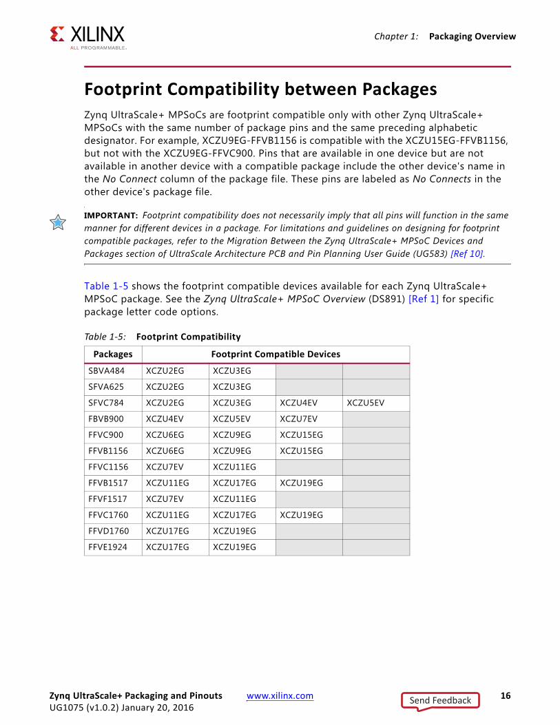
Footprint Compatibility between PackagesZynq UltraScale+ MPSoCs are footprint compatible only with other Zynq UltraScale+ MPSoCs with the same number of package pins and the same preceding alphabetic designator. For example, XCZU9EG-FFVB1156 is compatible with the XCZU15EG-FFVB1156, but not with the XCZU9EG-FFVC900. Pins that are available in one device but are not available in another device with a compatible package include the other device's name in the No Connect column of the package file. These pins are labeled as No Connects in the other device's package file.
IMPORTANT: Footprint compatibility does not necessarily imply that all pins will function in the same manner for different devices in a package. For limitations and guidelines on designing for footprint compatible packages, refer to the Migration Between the Zynq UltraScale+ MPSoC Devices and Packages section of UltraScale Architecture PCB and Pin Planning User Guide (UG583) [Ref 10].
Table 1-5 shows the footprint compatible devices available for each Zynq UltraScale+ MPSoC package. See the Zynq UltraScale+ MPSoC Overview (DS891) [Ref 1] for specific package letter code options.
Table 1-5: Footprint Compatibility
Packages Footprint Compatible Devices
SBVA484 XCZU2EG XCZU3EG
SFVA625 XCZU2EG XCZU3EG
SFVC784 XCZU2EG XCZU3EG XCZU4EV XCZU5EV
FBVB900 XCZU4EV XCZU5EV XCZU7EV
FFVC900 XCZU6EG XCZU9EG XCZU15EG
FFVB1156 XCZU6EG XCZU9EG XCZU15EG
FFVC1156 XCZU7EV XCZU11EG
FFVB1517 XCZU11EG XCZU17EG XCZU19EG
FFVF1517 XCZU7EV XCZU11EG
FFVC1760 XCZU11EG XCZU17EG XCZU19EG
FFVD1760 XCZU17EG XCZU19EG
FFVE1924 XCZU17EG XCZU19EG
Zynq UltraScale+ Packaging and Pinouts www.xilinx.com 16UG1075 (v1.0.2) January 20, 2016
Send Feedback
Chapter 1: Packaging Overview
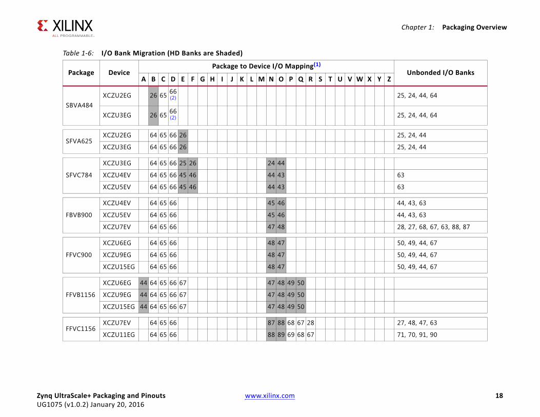
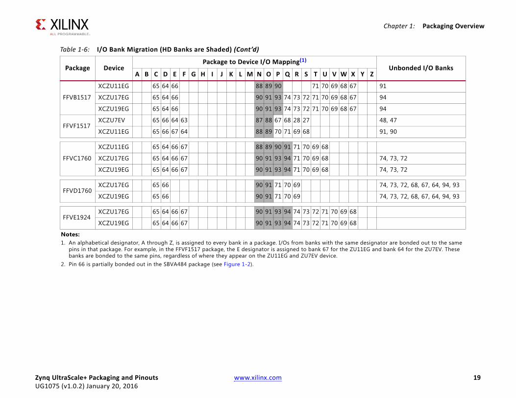
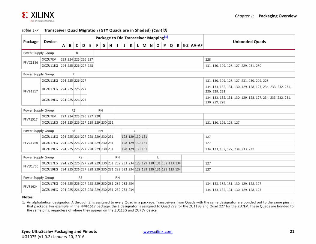
Many Zynq UltraScale+ MPSoCs that are footprint compatible in a package have different I/O bank and transceiver quad numbers connected to the same package pins. Due to these differences, when migrating between devices in a specific package, the type of bank (HD vs. HP) or quad (PS-GTR, GTH, or GTY), whether a bank is connected or NC at the package pins, and where the bank or quad is located on the die must be taken into consideration. Table 1-6 and Table 1-7 show how the banks and transceiver quads are numbered between devices in each package.
For all grouped-together footprint-compatible packages, the bank and quad numbers in the same column (indicated by the letters A through Z) for each device are connected to the same package pins. For example, in the FFVB1517 packages, bank 88 for the XCZU11EG is connected to the same pins as bank 90 for the XCZU17EG and XCZU19EG.
A limited number of HP I/O banks have fewer than 52 SelectIO pins. For a visual representation of all of this information, see the Die Level Bank Numbering Overview section.
Zynq UltraScale+ Packaging and Pinouts www.xilinx.com 17UG1075 (v1.0.2) January 20, 2016
Send Feedback
Chapter 1: Packaging Overview
Zy 18UG
Unbonded I/O BanksY Z
25, 24, 44, 64
25, 24, 44, 64
25, 24, 44
25, 24, 44
63
63
44, 43, 63
44, 43, 63
28, 27, 68, 67, 63, 88, 87
50, 49, 44, 67
50, 49, 44, 67
50, 49, 44, 67
27, 48, 47, 63
71, 70, 91, 90
nq UltraScale+ Packaging and Pinouts www.xilinx.com1075 (v1.0.2) January 20, 2016
Table 1-6: I/O Bank Migration (HD Banks are Shaded)
Package DevicePackage to Device I/O Mapping(1)
A B C D E F G H I J K L M N O P Q R S T U V W X
SBVA484XCZU2EG 26 65 66
(2)
XCZU3EG 26 65 66(2)
SFVA625XCZU2EG 64 65 66 26
XCZU3EG 64 65 66 26
SFVC784
XCZU3EG 64 65 66 25 26 24 44
XCZU4EV 64 65 66 45 46 44 43
XCZU5EV 64 65 66 45 46 44 43
FBVB900
XCZU4EV 64 65 66 45 46
XCZU5EV 64 65 66 45 46
XCZU7EV 64 65 66 47 48
FFVC900
XCZU6EG 64 65 66 48 47
XCZU9EG 64 65 66 48 47
XCZU15EG 64 65 66 48 47
FFVB1156
XCZU6EG 44 64 65 66 67 47 48 49 50
XCZU9EG 44 64 65 66 67 47 48 49 50
XCZU15EG 44 64 65 66 67 47 48 49 50
FFVC1156XCZU7EV 64 65 66 87 88 68 67 28
XCZU11EG 64 65 66 88 89 69 68 67
Chapter 1: Packaging Overview
Zy 19UG
91
94
94
48, 47
91, 90
74, 73, 72
74, 73, 72
74, 73, 72, 68, 67, 64, 94, 93
74, 73, 72, 68, 67, 64, 94, 93
designator are bonded out to the same 1EG and bank 64 for the ZU7EV. These
Unbonded I/O BanksY Z
nq UltraScale+ Packaging and Pinouts www.xilinx.com1075 (v1.0.2) January 20, 2016
FFVB1517
XCZU11EG 65 64 66 88 89 90 71 70 69 68 67
XCZU17EG 65 64 66 90 91 93 74 73 72 71 70 69 68 67
XCZU19EG 65 64 66 90 91 93 74 73 72 71 70 69 68 67
FFVF1517XCZU7EV 65 66 64 63 87 88 67 68 28 27
XCZU11EG 65 66 67 64 88 89 70 71 69 68
FFVC1760
XCZU11EG 65 64 66 67 88 89 90 91 71 70 69 68
XCZU17EG 65 64 66 67 90 91 93 94 71 70 69 68
XCZU19EG 65 64 66 67 90 91 93 94 71 70 69 68
FFVD1760XCZU17EG 65 66 90 91 71 70 69
XCZU19EG 65 66 90 91 71 70 69
FFVE1924XCZU17EG 65 64 66 67 90 91 93 94 74 73 72 71 70 69 68
XCZU19EG 65 64 66 67 90 91 93 94 74 73 72 71 70 69 68
Notes: 1. An alphabetical designator, A through Z, is assigned to every bank in a package. I/Os from banks with the same
pins in that package. For example, in the FFVF1517 package, the E designator is assigned to bank 67 for the ZU1banks are bonded to the same pins, regardless of where they appear on the ZU11EG and ZU7EV device.
2. Pin 66 is partially bonded out in the SBVA484 package (see Figure 1-2).
Table 1-6: I/O Bank Migration (HD Banks are Shaded) (Cont’d)
Package DevicePackage to Device I/O Mapping(1)
A B C D E F G H I J K L M N O P Q R S T U V W X

Chapter 1: Packaging Overview
Zy 20UG
etailing the power supply group for upply pins, as listed in the ASCII
information, see the Die Level Bank
Ta
P Unbonded Quads
SB
SF
P
SF223
223
P
FB
P
FF
127
127
127
P
FF
nq UltraScale+ Packaging and Pinouts www.xilinx.com1075 (v1.0.2) January 20, 2016
For each grouped set of footprint compatible packages listed in Table 1-7, there is a row deach Quad. These groups are labeled according to the regions for the transceiver power sPinout Files linked from Chapter 2, Package Files. For a visual representation of all of thisNumbering Overview section.
ble 1-7: Transceiver Quad Migration (GTY Quads are in Shaded)
ackage DevicePackage to Die Transceiver Mapping(1)
A B C D E F G H I J K L M N O P Q R S-Z AA-AF
VA484XCZU2EG
XCZU3EG
VA625XCZU2EG
XCZU3EG
ower Supply Group R
VC784
XCZU2EG
XCZU3EG
XCZU4EV 224 226, 225,
XCZU5EV 224 226, 225,
ower Supply Group R
VB900
XCZU4EV 223 224 225 226
XCZU5EV 223 224 225 226
XCZU7EV 223 224 225 226 228, 227
ower Supply Group R L
VC900
XCZU6EG 228 229 230 128 130, 129,
XCZU9EG 228 229 230 128 130, 129,
XCZU15EG 228 229 230 128 130, 129,
ower Supply Group R L
VB1156
XCZU6EG 228 229 230 128 129 130 127
XCZU9EG 228 229 230 128 129 130 127
XCZU15EG 228 229 230 128 129 130 127
Chapter 1: Packaging Overview
Zy 21UG
P
FF129, 128, 127, 229, 231, 230
P
FF
129, 128, 127, 231, 230, 229, 228
132, 131, 130, 129, 128, 127, 234, 233, 232, 231, 228
132, 131, 130, 129, 128, 127, 234, 233, 232, 231, 228
P
FF129, 128, 127
P
FF
132, 127, 234, 233, 232
P
FF
P
FF132, 131, 130, 129, 128, 127
132, 131, 130, 129, 128, 127
No1. designator are bonded out to the same pins in
227 for the ZU7EV. These Quads are bonded to
Ta
P Unbonded Quads
nq UltraScale+ Packaging and Pinouts www.xilinx.com1075 (v1.0.2) January 20, 2016
ower Supply Group R
VC1156XCZU7EV 223 224 225 226 227 228
XCZU11EG 224 225 226 227 228 131, 130,
ower Supply Group R
VB1517
XCZU11EG 224 225 226 227 131, 130,
XCZU17EG 224 225 226 227134, 133, 230, 229,
XCZU19EG 224 225 226 227134, 133, 230, 229,
ower Supply Group RS RN
VF1517XCZU7EV 223 224 225 226 227 228
XCZU11EG 224 225 226 227 228 229 230 231 131, 130,
ower Supply Group RS RN L
VC1760
XCZU11EG 224 225 226 227 228 229 230 231 128 129 130 131 127
XCZU17EG 224 225 226 227 228 229 230 231 128 129 130 131 127
XCZU19EG 224 225 226 227 228 229 230 231 128 129 130 131 134, 133,
ower Supply Group RS RN L
VD1760XCZU17EG 224 225 226 227 228 229 230 231 232 233 234 128 129 130 131 132 133 134 127
XCZU19EG 224 225 226 227 228 229 230 231 232 233 234 128 129 130 131 132 133 134 127
ower Supply Group RS RN
VE1924XCZU17EG 224 225 226 227 228 229 230 231 232 233 234 134, 133,
XCZU19EG 224 225 226 227 228 229 230 231 232 233 234 134, 133,
tes: An alphabetical designator, A through Z, is assigned to every Quad in a package. Transceivers from Quads with the same that package. For example, in the FFVF1517 package, the E designator is assigned to Quad 228 for the ZU11EG and Quad the same pins, regardless of where they appear on the ZU11EG and ZU7EV device.
ble 1-7: Transceiver Quad Migration (GTY Quads are in Shaded) (Cont’d)
ackage DevicePackage to Die Transceiver Mapping(1)
A B C D E F G H I J K L M N O P Q R S-Z AA-AF

Chapter 1: Packaging Overview
Die Level Bank Numbering OverviewBanking and Clocking Summary
• For each device, not all banks are bonded out in every package.
GTH/GTY Columns
• One GT Quad = Four transceivers = Four GTHE4 or GTYE4 primitives.
• Not all GT Quads are bonded out in every package.
• Also shown are quads labeled with RCAL. This specifies the location of the RCAL masters for each device. With respect to the package, the RCAL masters are located on the same package pin for each package, regardless of the device.
I/O Banks
• Each user HP I/O bank has a total of 52 I/Os where 48 can be used as differential (24 differential pairs) or single-ended I/Os. The remaining four function only as single-ended I/Os. All 52 pads of a bank are not always bonded out to pins.
• A limited number of HP I/O banks have fewer than 52 SelectIO pins. These banks are signified by the notation partial.
• Each user HD I/O bank has a total of 24 I/Os that can be used as differential (12 differential pairs) or single-ended I/Os.
• Adjacent to each bank is a physical layer (PHY) containing a CMT and other clock resources.
• Adjacent to each bank and PHY is a tile of logic resources that makes up a clock region.
• Banks are arranged in columns and separated into rows which are pitch-matched with adjacent PHY, clock regions, and GT blocks.
Clocking
• Each bank has four pairs of global clock (GC or HDGC) inputs for four differential or four single-ended clock inputs. Single-ended clock inputs should be connected to the P-side of the differential pair.
• Clock signals are distributed through global buffers driving routing and distribution networks to reach any clock region, I/O, or GT.
• Global clock inputs can connect to an MMCM and two PLLs within the horizontally adjacent CMT.
Zynq UltraScale+ Packaging and Pinouts www.xilinx.com 22UG1075 (v1.0.2) January 20, 2016
Send Feedback
Chapter 1: Packaging Overview
Bank Locations of Dedicated and Multi-Function Pins
• In all Zynq UltraScale+ MPSoCs, bank 0 contains the dedicated PUDC_B configuration pin.
• All dedicated configuration I/Os (bank 0) and HD I/Os are 3.3V capable.
Processor (PS) Blocks
• MIO pins are shared between banks 500, 501, and 502.
• Configuration pins are in bank 503.
• DDR memory pins are in bank 504.
• Transceiver pins are in the PS-GTR quad 505.
SYSMON, Configuration, PCIe, Interlaken, and 100GE Integrated Blocks
• Configuration: Configuration block.
• SYSMON/Configuration: Block shared between the SYSMONE4 and configuration.
• PCIe: Integrated block for PCIe.
Note: PCIe blocks with an additional (Tandem) label support tandem configuration.
• ILKN: Interlaken block.
• CMAC: 100G Ethernet block.
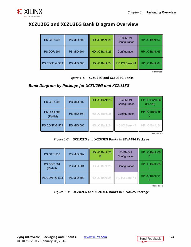
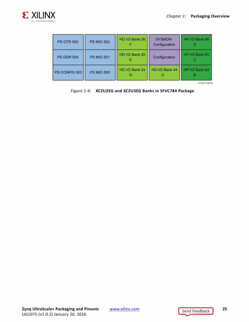
Device DiagramsFigure 1-1 through Figure 1-27 visually describe a die view of each device bank numbering. The first figure in the series is not package specific and shows all resources. The following figures in the series show the resources available by package. The available resources by device and package are detailed in the Zynq UltraScale+ MPSoC Overview (DS891) [Ref 1].
Zynq UltraScale+ Packaging and Pinouts www.xilinx.com 23UG1075 (v1.0.2) January 20, 2016
Send Feedback
Chapter 1: Packaging Overview
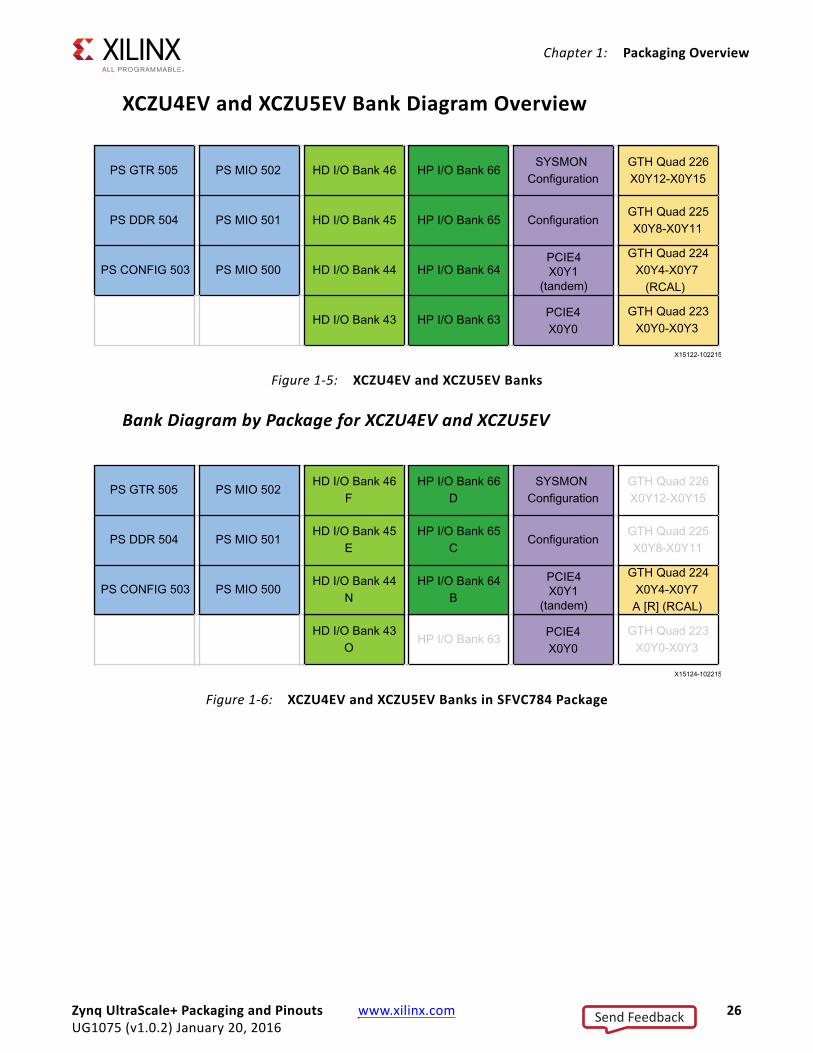
XCZU2EG and XCZU3EG Bank Diagram Overview
Bank Diagram by Package for XCZU2EG and XCZU3EG
X-Ref Target - Figure 1-1
Figure 1-1: XCZU2EG and XCZU3EG Banks
X-Ref Target - Figure 1-2
Figure 1-2: XCZU2EG and XCZU3EG Banks in SBVA484 Package
X-Ref Target - Figure 1-3
Figure 1-3: XCZU2EG and XCZU3EG Banks in SFVA625 Package
Zynq UltraScale+ Packaging and Pinouts www.xilinx.com 24UG1075 (v1.0.2) January 20, 2016
Send Feedback
Chapter 1: Packaging Overview
X-Ref Target - Figure 1-4
Figure 1-4: XCZU2EG and XCZU3EG Banks in SFVC784 Package
Zynq UltraScale+ Packaging and Pinouts www.xilinx.com 25UG1075 (v1.0.2) January 20, 2016
Send Feedback
Chapter 1: Packaging Overview
XCZU4EV and XCZU5EV Bank Diagram Overview
Bank Diagram by Package for XCZU4EV and XCZU5EV
X-Ref Target - Figure 1-5
Figure 1-5: XCZU4EV and XCZU5EV Banks
X-Ref Target - Figure 1-6
Figure 1-6: XCZU4EV and XCZU5EV Banks in SFVC784 Package
Zynq UltraScale+ Packaging and Pinouts www.xilinx.com 26UG1075 (v1.0.2) January 20, 2016
Send Feedback
Chapter 1: Packaging Overview
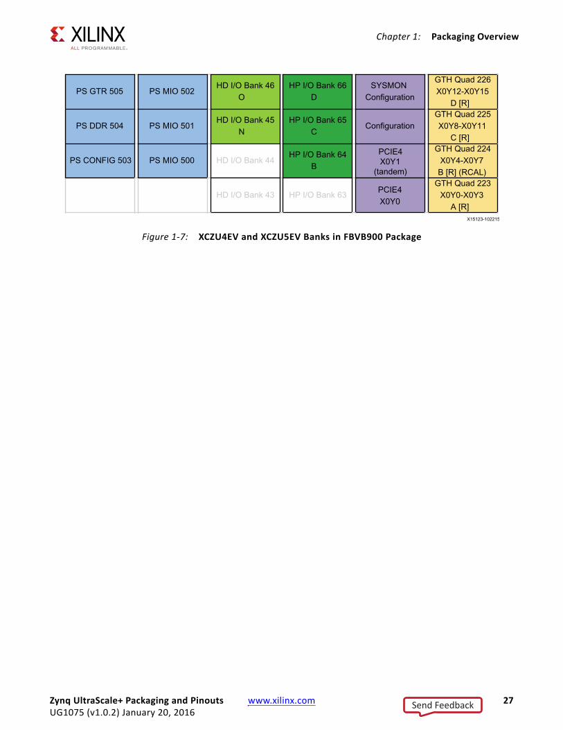
X-Ref Target - Figure 1-7
Figure 1-7: XCZU4EV and XCZU5EV Banks in FBVB900 Package
Zynq UltraScale+ Packaging and Pinouts www.xilinx.com 27UG1075 (v1.0.2) January 20, 2016
Send Feedback
Chapter 1: Packaging Overview
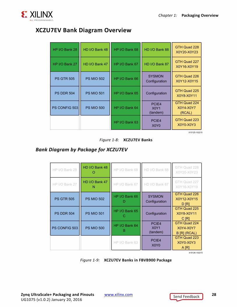
XCZU7EV Bank Diagram Overview
Bank Diagram by Package for XCZU7EV
X-Ref Target - Figure 1-8
Figure 1-8: XCZU7EV Banks
X-Ref Target - Figure 1-9
Figure 1-9: XCZU7EV Banks in FBVB900 Package
Zynq UltraScale+ Packaging and Pinouts www.xilinx.com 28UG1075 (v1.0.2) January 20, 2016
Send Feedback
Chapter 1: Packaging Overview
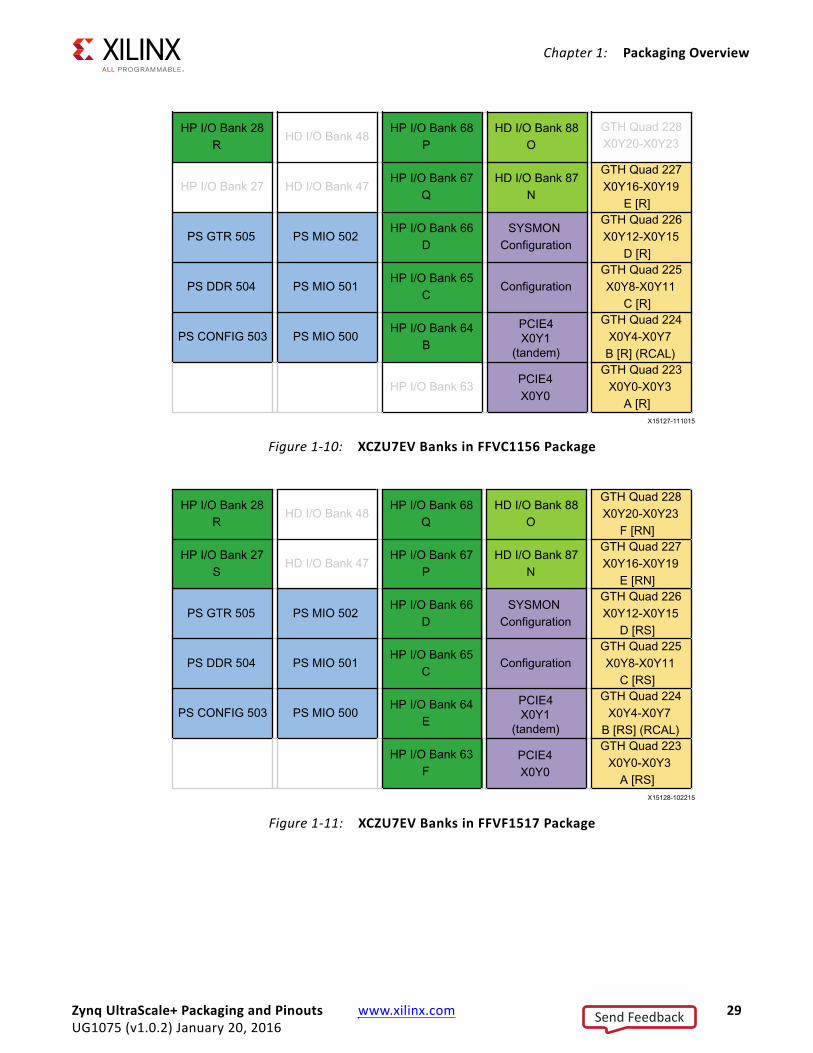
X-Ref Target - Figure 1-10
Figure 1-10: XCZU7EV Banks in FFVC1156 Package
X-Ref Target - Figure 1-11
Figure 1-11: XCZU7EV Banks in FFVF1517 Package
Zynq UltraScale+ Packaging and Pinouts www.xilinx.com 29UG1075 (v1.0.2) January 20, 2016
Send Feedback
Chapter 1: Packaging Overview
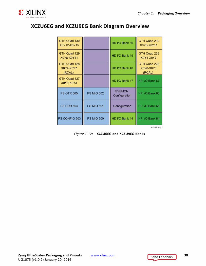
XCZU6EG and XCZU9EG Bank Diagram OverviewX-Ref Target - Figure 1-12
Figure 1-12: XCZU6EG and XCZU9EG Banks
Zynq UltraScale+ Packaging and Pinouts www.xilinx.com 30UG1075 (v1.0.2) January 20, 2016
Send Feedback
Chapter 1: Packaging Overview
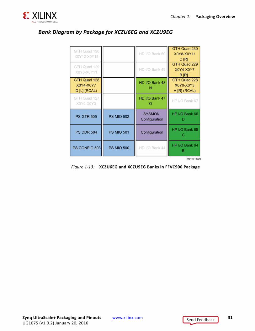
Bank Diagram by Package for XCZU6EG and XCZU9EGX-Ref Target - Figure 1-13
Figure 1-13: XCZU6EG and XCZU9EG Banks in FFVC900 Package
Zynq UltraScale+ Packaging and Pinouts www.xilinx.com 31UG1075 (v1.0.2) January 20, 2016
Send Feedback
Chapter 1: Packaging Overview
X-Ref Target - Figure 1-14
Figure 1-14: XCZU6EG and XCZU9EG Banks in FFVB1156 Package
Zynq UltraScale+ Packaging and Pinouts www.xilinx.com 32UG1075 (v1.0.2) January 20, 2016
Send Feedback
Chapter 1: Packaging Overview
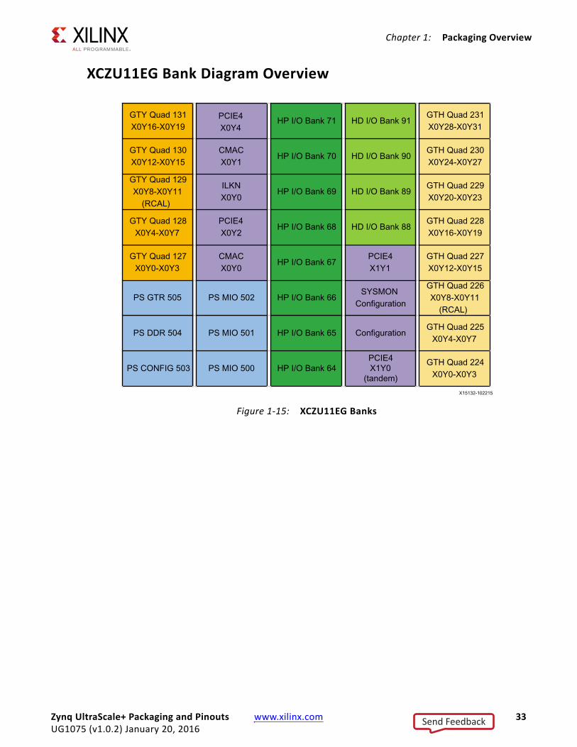
XCZU11EG Bank Diagram OverviewX-Ref Target - Figure 1-15
Figure 1-15: XCZU11EG Banks
Zynq UltraScale+ Packaging and Pinouts www.xilinx.com 33UG1075 (v1.0.2) January 20, 2016
Send Feedback
Chapter 1: Packaging Overview
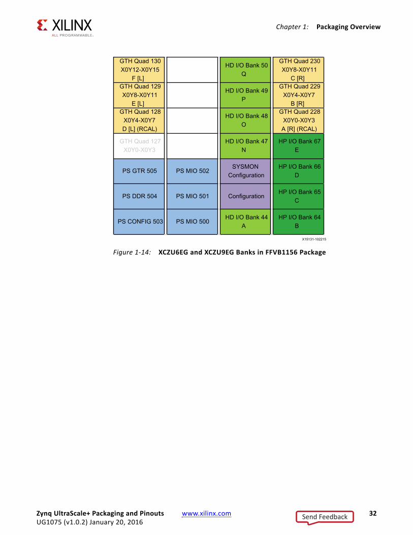
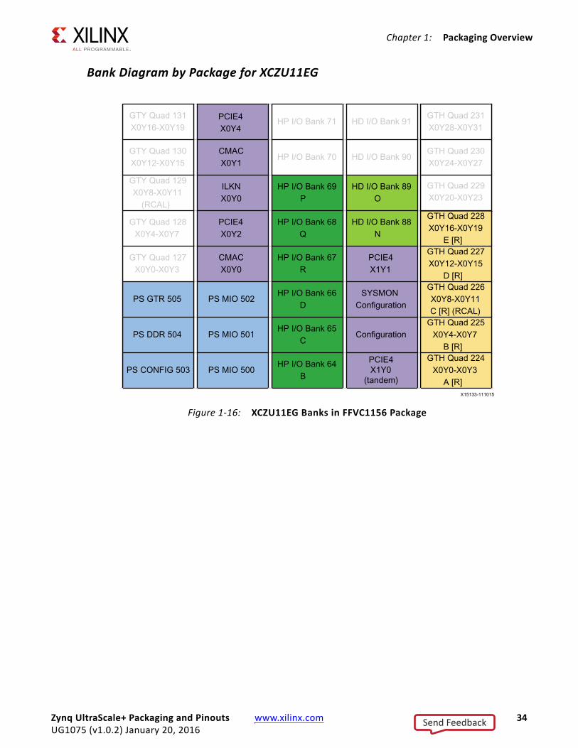
Bank Diagram by Package for XCZU11EGX-Ref Target - Figure 1-16
Figure 1-16: XCZU11EG Banks in FFVC1156 Package
Zynq UltraScale+ Packaging and Pinouts www.xilinx.com 34UG1075 (v1.0.2) January 20, 2016
Send Feedback
Chapter 1: Packaging Overview
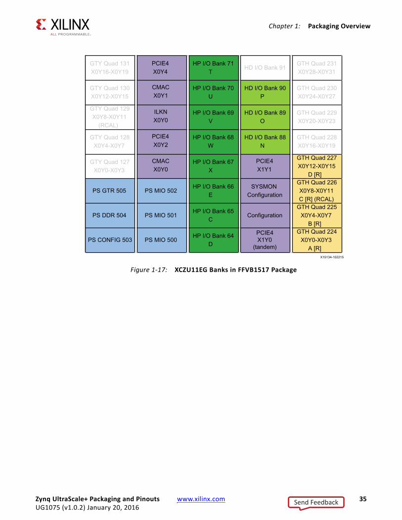
X-Ref Target - Figure 1-17
Figure 1-17: XCZU11EG Banks in FFVB1517 Package
Zynq UltraScale+ Packaging and Pinouts www.xilinx.com 35UG1075 (v1.0.2) January 20, 2016
Send Feedback
Chapter 1: Packaging Overview
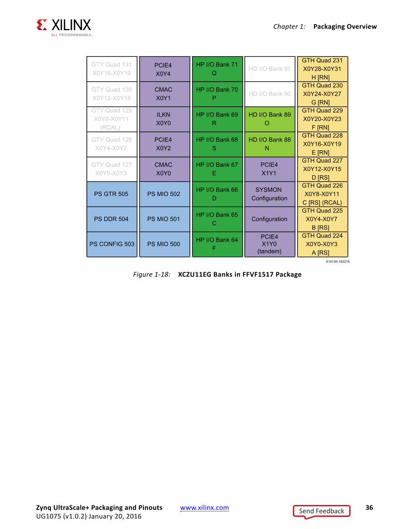
X-Ref Target - Figure 1-18
Figure 1-18: XCZU11EG Banks in FFVF1517 Package
Zynq UltraScale+ Packaging and Pinouts www.xilinx.com 36UG1075 (v1.0.2) January 20, 2016
Send Feedback
Chapter 1: Packaging Overview
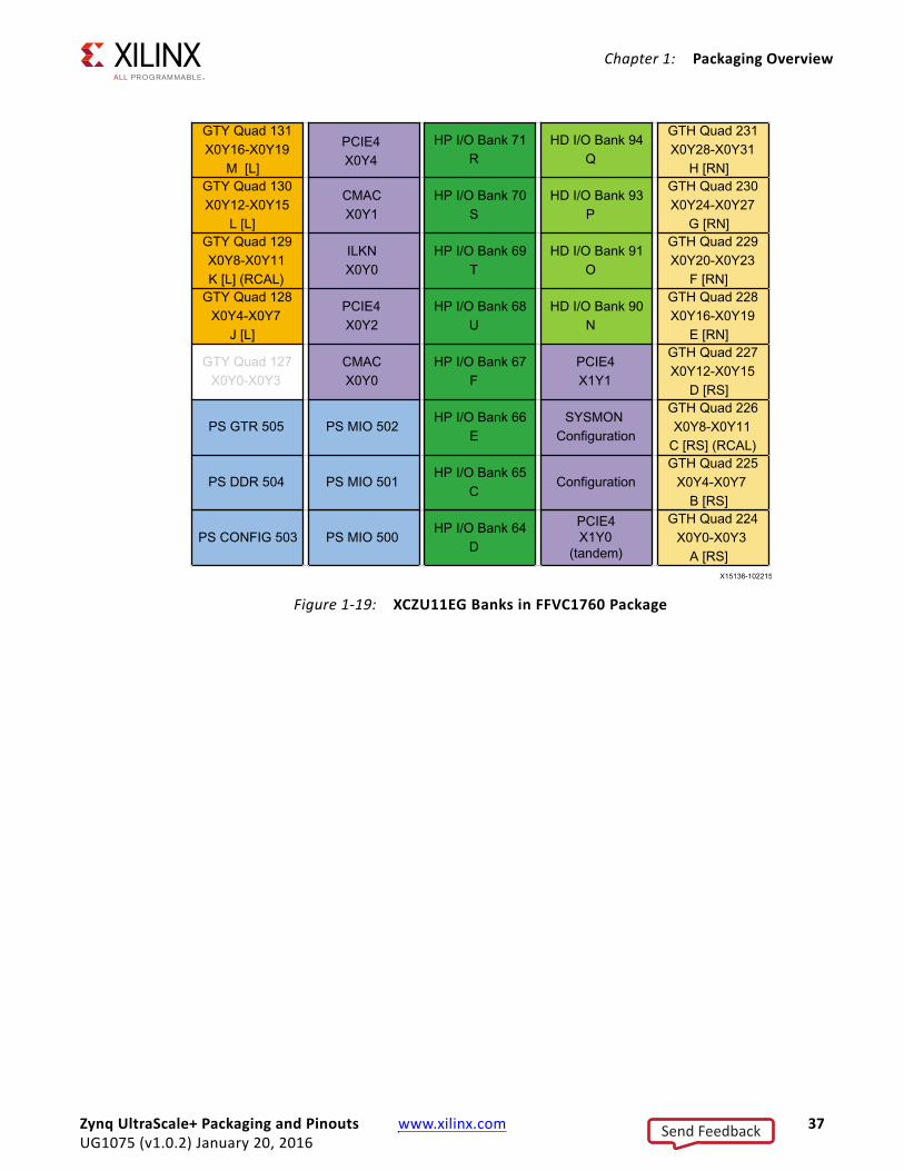
X-Ref Target - Figure 1-19
Figure 1-19: XCZU11EG Banks in FFVC1760 Package
Zynq UltraScale+ Packaging and Pinouts www.xilinx.com 37UG1075 (v1.0.2) January 20, 2016
Send Feedback
Chapter 1: Packaging Overview
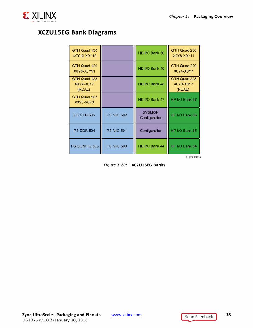
XCZU15EG Bank DiagramsX-Ref Target - Figure 1-20
Figure 1-20: XCZU15EG Banks
Zynq UltraScale+ Packaging and Pinouts www.xilinx.com 38UG1075 (v1.0.2) January 20, 2016
Send Feedback
Chapter 1: Packaging Overview
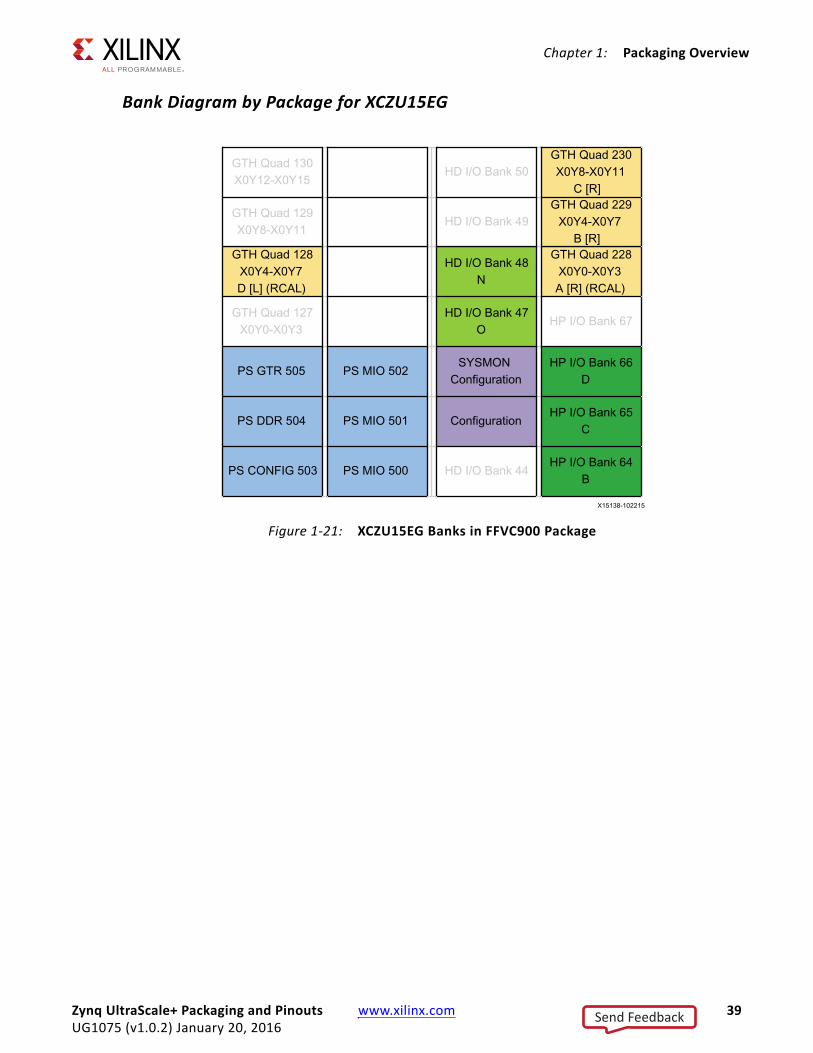
Bank Diagram by Package for XCZU15EGX-Ref Target - Figure 1-21
Figure 1-21: XCZU15EG Banks in FFVC900 Package
Zynq UltraScale+ Packaging and Pinouts www.xilinx.com 39UG1075 (v1.0.2) January 20, 2016
Send Feedback

Chapter 1: Packaging Overview
X-Ref Target - Figure 1-22
Figure 1-22: XCZU15EG Banks in FFVB1156 Package
Zynq UltraScale+ Packaging and Pinouts www.xilinx.com 40UG1075 (v1.0.2) January 20, 2016
Send Feedback
Chapter 1: Packaging Overview
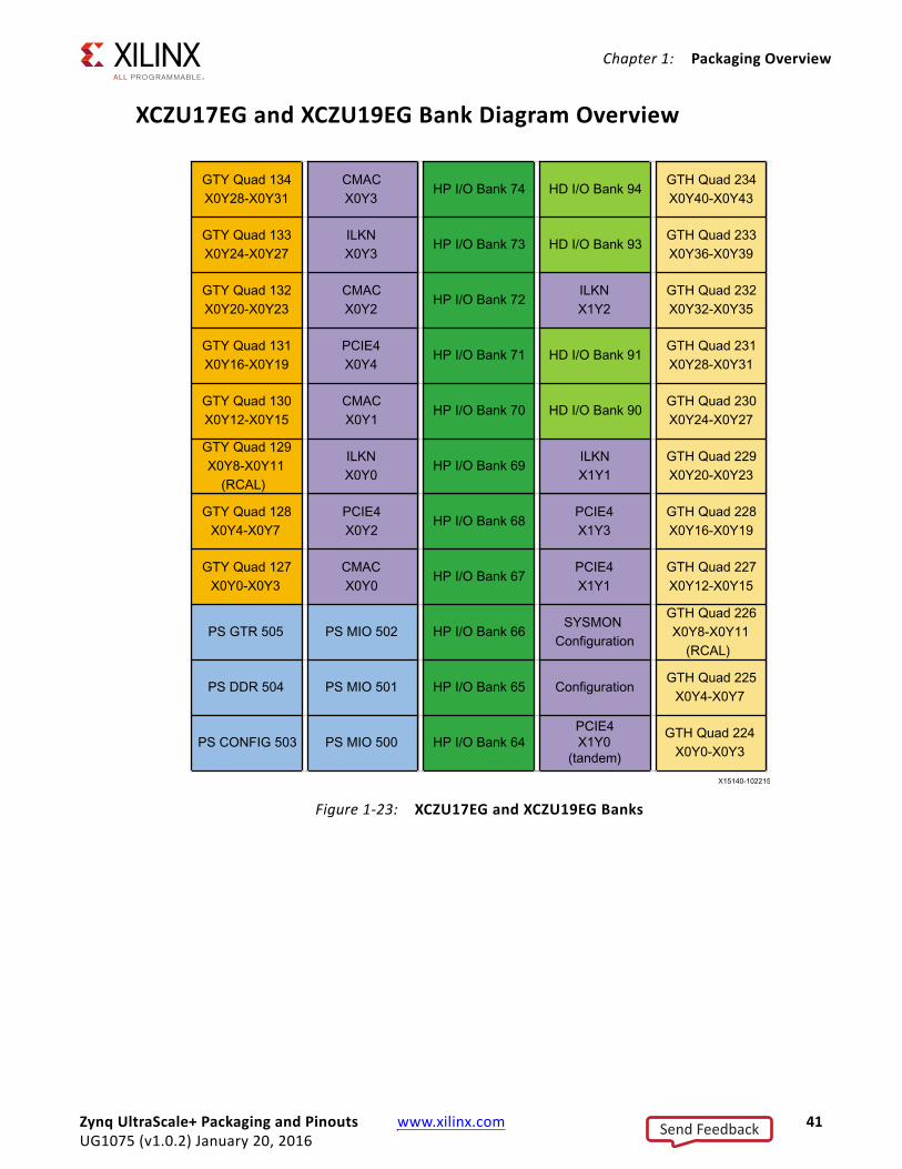
XCZU17EG and XCZU19EG Bank Diagram OverviewX-Ref Target - Figure 1-23
Figure 1-23: XCZU17EG and XCZU19EG Banks
Zynq UltraScale+ Packaging and Pinouts www.xilinx.com 41UG1075 (v1.0.2) January 20, 2016
Send Feedback
Chapter 1: Packaging Overview
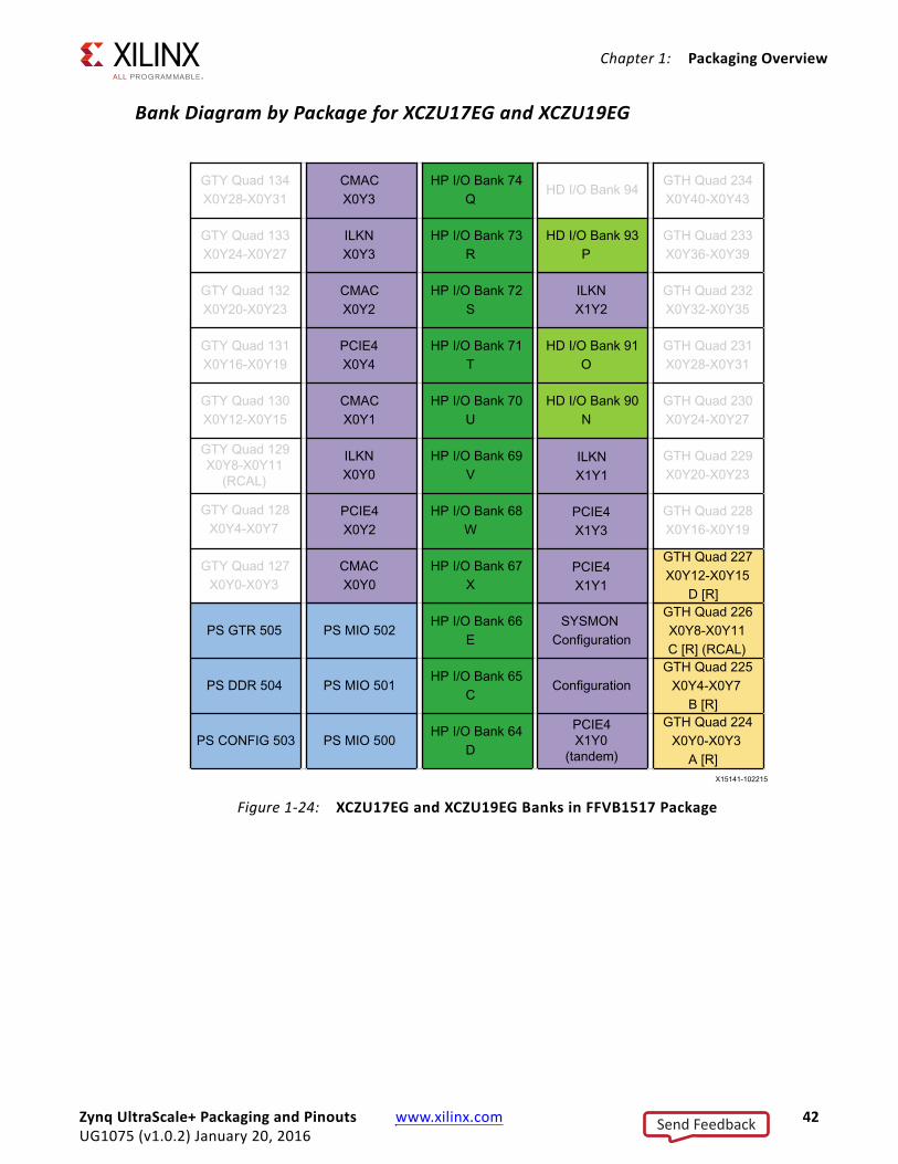
Bank Diagram by Package for XCZU17EG and XCZU19EGX-Ref Target - Figure 1-24
Figure 1-24: XCZU17EG and XCZU19EG Banks in FFVB1517 Package
Zynq UltraScale+ Packaging and Pinouts www.xilinx.com 42UG1075 (v1.0.2) January 20, 2016
Send Feedback
Chapter 1: Packaging Overview
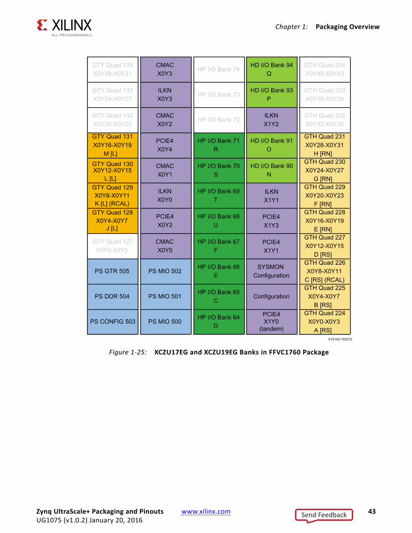
X-Ref Target - Figure 1-25
Figure 1-25: XCZU17EG and XCZU19EG Banks in FFVC1760 Package
Zynq UltraScale+ Packaging and Pinouts www.xilinx.com 43UG1075 (v1.0.2) January 20, 2016
Send Feedback
Chapter 1: Packaging Overview
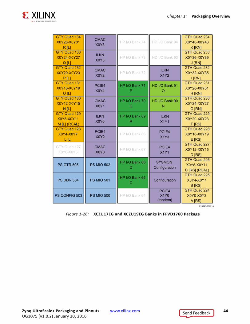
X-Ref Target - Figure 1-26
Figure 1-26: XCZU17EG and XCZU19EG Banks in FFVD1760 Package
Zynq UltraScale+ Packaging and Pinouts www.xilinx.com 44UG1075 (v1.0.2) January 20, 2016
Send Feedback
Chapter 1: Packaging Overview
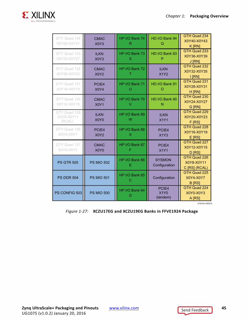
X-Ref Target - Figure 1-27
Figure 1-27: XCZU17EG and XCZU19EG Banks in FFVE1924 Package
Zynq UltraScale+ Packaging and Pinouts www.xilinx.com 45UG1075 (v1.0.2) January 20, 2016
Send Feedback
Chapter 2
Package Files
About ASCII Package FilesThe ASCII package files for each package include a comma-separated-values (CSV) version and a text version optimized for a browser or text editor in fixed-width fonts. The information in each of the files includes:
• Device/Package name (family-device-package), with date and time of creation
• Seven columns containing data for each pin:
° Pin—Pin location on the package.
° Pin Name—The name of the assigned pin.
° Memory Byte Group—Memory byte group between 0 and 3 split into upper (U) and lower (L) halves. For more information on the memory byte group, see the UltraScale Architecture-Based Memory Interface Solutions Product Guide (PG150) [Ref 11].
° Bank—Bank number.
° I/O Type—CONFIG, HD, HP, GTH, GTY, PS-GTR, PSMIO, PSDDR, or PSCONFIG depends on the I/O type. For more information on the I/O type, see the UltraScale Architecture SelectIO Resources User Guide (UG571) [Ref 3].
° No-Connect—This list of devices is used for migration between devices that have the same package size and are not connected at that specific pin.
• Total number of pins in the package.
Zynq UltraScale+ Packaging and Pinouts www.xilinx.com 46UG1075 (v1.0.2) January 20, 2016
Send Feedback
Chapter 2: Package Files
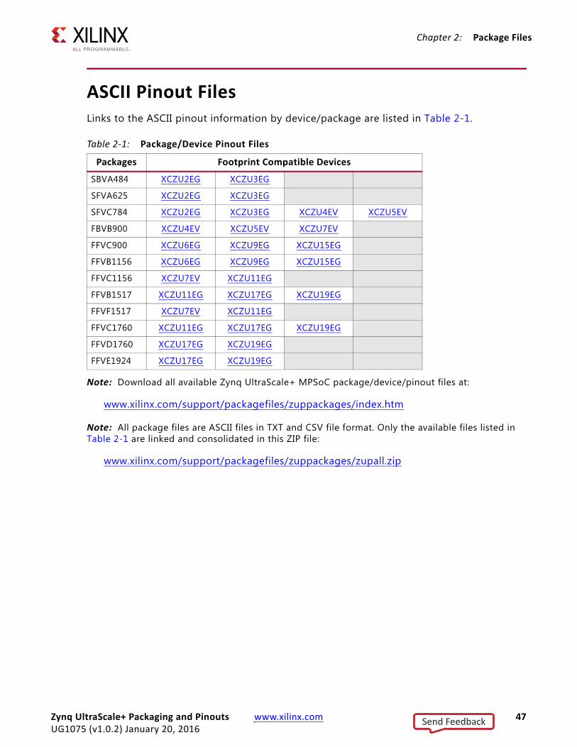
ASCII Pinout FilesLinks to the ASCII pinout information by device/package are listed in Table 2-1.
Note: Download all available Zynq UltraScale+ MPSoC package/device/pinout files at:
www.xilinx.com/support/packagefiles/zuppackages/index.htm
Note: All package files are ASCII files in TXT and CSV file format. Only the available files listed in Table 2-1 are linked and consolidated in this ZIP file:
www.xilinx.com/support/packagefiles/zuppackages/zupall.zip
Table 2-1: Package/Device Pinout Files
Packages Footprint Compatible Devices
SBVA484 XCZU2EG XCZU3EG
SFVA625 XCZU2EG XCZU3EG
SFVC784 XCZU2EG XCZU3EG XCZU4EV XCZU5EV
FBVB900 XCZU4EV XCZU5EV XCZU7EV
FFVC900 XCZU6EG XCZU9EG XCZU15EG
FFVB1156 XCZU6EG XCZU9EG XCZU15EG
FFVC1156 XCZU7EV XCZU11EG
FFVB1517 XCZU11EG XCZU17EG XCZU19EG
FFVF1517 XCZU7EV XCZU11EG
FFVC1760 XCZU11EG XCZU17EG XCZU19EG
FFVD1760 XCZU17EG XCZU19EG
FFVE1924 XCZU17EG XCZU19EG
Zynq UltraScale+ Packaging and Pinouts www.xilinx.com 47UG1075 (v1.0.2) January 20, 2016
Send Feedback
Chapter 3
Device Diagrams
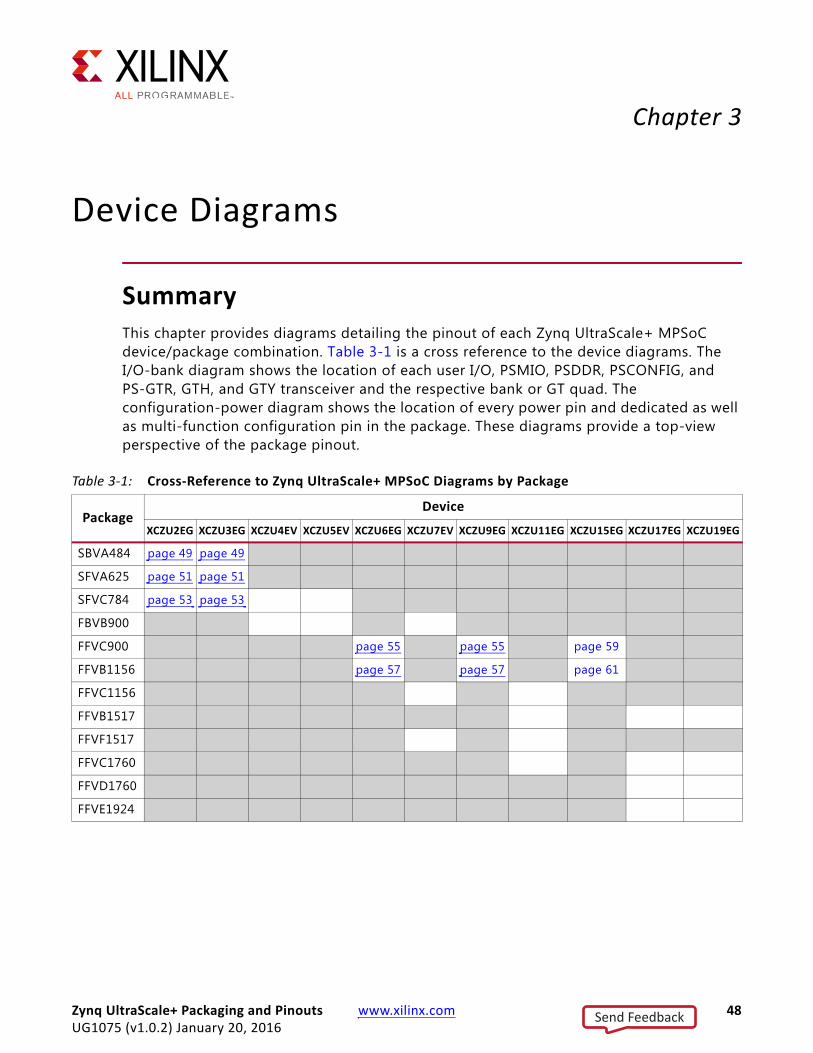
SummaryThis chapter provides diagrams detailing the pinout of each Zynq UltraScale+ MPSoC device/package combination. Table 3-1 is a cross reference to the device diagrams. The I/O-bank diagram shows the location of each user I/O, PSMIO, PSDDR, PSCONFIG, and PS-GTR, GTH, and GTY transceiver and the respective bank or GT quad. The configuration-power diagram shows the location of every power pin and dedicated as well as multi-function configuration pin in the package. These diagrams provide a top-view perspective of the package pinout.
Table 3-1: Cross-Reference to Zynq UltraScale+ MPSoC Diagrams by Package
PackageDevice
XCZU2EG XCZU3EG XCZU4EV XCZU5EV XCZU6EG XCZU7EV XCZU9EG XCZU11EG XCZU15EG XCZU17EG XCZU19EG
SBVA484 page 49 page 49
SFVA625 page 51 page 51
SFVC784 page 53 page 53
FBVB900
FFVC900 page 55 page 55 page 59
FFVB1156 page 57 page 57 page 61
FFVC1156
FFVB1517
FFVF1517
FFVC1760
FFVD1760
FFVE1924
Zynq UltraScale+ Packaging and Pinouts www.xilinx.com 48UG1075 (v1.0.2) January 20, 2016
Send Feedback

Chapter 3: Device Diagrams
SBVA484 Package–XCZU2EG and XCZU3EGX-Ref Target - Figure 3-1
Figure 3-1: SBVA484 Package—XCZU2EG and XCZU3EG I/O Bank Diagram
121211 1110 10 9
98 87
7 66
5 5
4 43 3
221 1
S 12 1211 11
2424
23 23
222221
21 20 201919
S
S1818
1717 16
161515 14 14
13 13
12 1211 1110 10 9 9
8 87
7 S
66
55
44
3 3
22
1 10 1
10 11
12 13 14 15 16
17 18 19
2
20 21
22 23 24 25
3 4 5 6
7 8 9
26 27 28 29
30 31 32 33
34 35 36 37
38 39 40 41
42 43 44 45
46 47 48
49 50 51
52 53 54 55
56 57 58 59
60 61 62
63 64 65 66
67 68 69
70 71 72 73
74 75 76
77
DN
EO ESIN
CKDI
DOMS MD
MD
MD
MDPI
PO
PR PG
RC
SR
A
A
A
AA AAA
A
A
A A AA
AA
A
A
AC
AL
BA
BA
BG
BG
CC
CECE
CN
CN CS
CS
DM DM
DM
DM
DM
0
1
10
11
12
13
14
15
1617
18 19
2
20
21
22
23
24 25
2627
28
29
3 30
31
4
5
6
64
65
66
67
68
69
7
70 71
8
9
N N
N N
N
P P
P P
P
ODOD
PA
RS ZQ
0505
1505
2505
3505
0
1
2
3
0505
1505
2505
3505
0
1
2
3
0505
0
1505
1
2505
2
3505
3
G
VCCO500
VCCO500
VCCO501
VCCO501
VCCO502VCCO502
VCCO503VCCO503
VCCO504
VCCO504
VCCO504
VCCO504
VCCO504
VCCO504
VCCO504
VCCO26
VCCO26
VCCO65
VCCO65
VCCO65
VCCO65
1
1
2
2
3
3
4
4
5
5
6
6
7
7
8
8
9
9
10
10
11
11
12
12
13
13
14
14
15
15
16
16
17
17
18
18
19
19
20
20
21
21
22
22
A AB BC CD DE EF FG GH HJ JK KL LM MN NP PR RT TU UV VW WY Y
AA AAAB AB
Bank 26Bank 65Bank 66PS Bank 500PS Bank 501PS Bank 502PS Bank 503PS Bank 504
PS Quad 505
SelectIO Pins
# IO_L#P
# IO_L#N
S IO (single−ended)
# IO_L#P_GC
# IO_L#N_GC
VRP
Dedicated Pins
VREF
V
MGTAVTTRCAL
G MGTRREF
Transceiver Pins# MGT[R, H or Y]RXP#
# MGT[R, H or Y]RXN## MGT[R, H or Y]TXP#
# MGT[R, H or Y]TXN## MGTREFCLK#P
# MGTREFCLK#N
PS Pins
# PS_MIO
# PS_DDR_DQP PS_DDR_DQS_PN PS_DDR_DQS_NAL PS_DDR_ALERT_NAC PS_DDR_ACT_NA PS_DDR_A
BA PS_DDR_BABG PS_DDR_BGCN PS_DDR_CK_NC PS_DDR_CK
CE PS_DDR_CKECS PS_DDR_CSDM PS_DDR_DMOD PS_DDR_ODTPA PS_DDR_PARITYRS PS_DDR_RAM_RST_NZQ PS_DDR_ZQ
DN PS_DONEEO PS_ERROR_OUTES PS_ERROR_STATUSIN PS_INIT_BCK PS_JTAG_TCKDI PS_JTAG_TDIDO PS_JTAG_TDOMS PS_JTAG_TMSMD PS_MODEPI PS_PADIPO PS_PADOPR PS_POR_BPG PS_PROG_BRC PS_REF_CLKSR PS_SRST_B
Zynq UltraScale+ Packaging and Pinouts www.xilinx.com 49UG1075 (v1.0.2) January 20, 2016
Send Feedback
Chapter 3: Device Diagrams
X-Ref Target - Figure 3-2
Figure 3-2: SBVA484 Package—XCZU2EG and XCZU3EG Configuration/Power Diagram
8 723
24 2122
1513
3534
33
AD
E
E
E
VV
V
AD
AU AU
AU AU
BT
DP DP
F P
F P F P
F P F P F P F P
D D
D D
D D
L P L P
L P L P
L P L P
PL PL
PL
1
1
2
2
3
3
4
4
5
5
6
6
7
7
8
8
9
9
10
10
11
11
12
12
13
13
14
14
15
15
16
16
17
17
18
18
19
19
20
20
21
21
22
22
A AB BC CD DE EF FG GH HJ JK KL LM MN NP PR RT TU UV VW WY Y
AA AAAB AB
Power Pins
GND
VBATT
VCCAUX_IO
VCCAUX
VCCINT
VCCINT_IO
VCCO_[bank number]
VCCBRAM
VCCADC
GNDADC
n NC
E MGTAVCC_[R or L]
V MGTAVTT_[R or L]
V
MGTVCCAUX_[R or L]
Dedicated Pins
7 DXP
8 DXN
13 POR_OVERRIDE
15 PUDC_B_0
21 VP
22 VN
23 VREFP
24 VREFN
Multi−Function I/O Pins
33 I2C_SCLK
34 I2C_SDA
35 PERSTN[0 to 1]
PS Pins
AD VCC_PSADC
AD GND_PSADC
AU VCC_PSAUX
E PS_MGTRAVCC
V PS_MGTRAVTT
BT VCC_PSBATT
DP VCC_PSDDR_PLL
PL VCC_PSPLL
F P VCC_PSINTFP
D D VCC_PSINTFP_DDR
L P VCC_PSINTLP
Zynq UltraScale+ Packaging and Pinouts www.xilinx.com 50UG1075 (v1.0.2) January 20, 2016
Send Feedback

Chapter 3: Device Diagrams
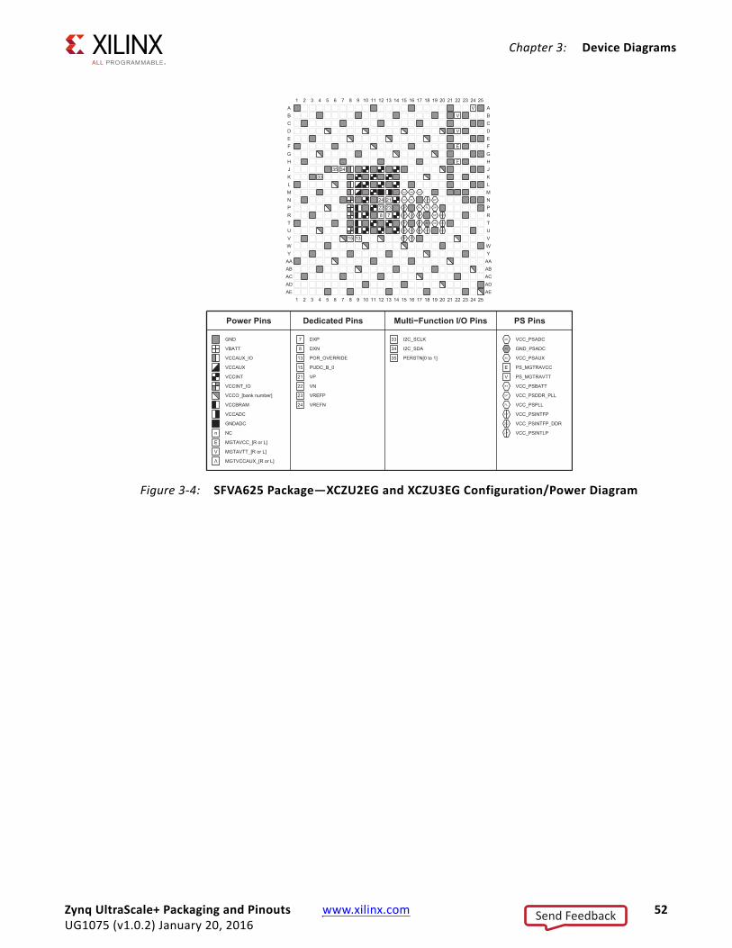
SFVA625 Package–XCZU2EG and XCZU3EGX-Ref Target - Figure 3-3
Figure 3-3: SFVA625 Package—XCZU2EG and XCZU3EG I/O Bank Diagram
121211
11
1010
9 9
8 877
66
55
44
33
22
11
242423
23
22 222121
2020
19 19
SS181817
17
1616
1515
14 1413 13
12 1211 11
10 10
9 9
8 877
S
6 6
55
44
3 3 22
11
24 242323 22
2221 21
2020
1919 S
S1818
17 17
16 16
1515
14 14
1313
12 121111 10 10
9 9 88
7 7 S66
5 5
44
33
22
1 1
24 242323
2222
21 21
20 20
1919
S
S
18 181717 16 16
1515
1414
1313
1212
1111
10 10
9 988
7 7
S
6 65 5
44
3 32 2
11
0
1 10
11
12
13
14
15
16
17
18
19
2
20
21
22
23
24
25
3
4
5
6 7
8
9
26
27
28
29
30
31
32
33
34
35
36
37
38
39
40
41
42
43
44
45
46
47
48
49
50
51
52
53
54
55
56
57 58
59
60
61 62
63
64
65
66
67
68
69
70
71 72
73
74
75
7677
DN
EO
ESIN
CK
DI DO MS
MDMD MD
MDPI PO
PRPG
RC
SR
A
A
A
A
A
A
A
A
A
A
A
A
A
A
A
A
A
A
AC
AL
BA
BABG BG
C
C
CE
CE
CNCN
CS
CS
DM
DM
DM
DM
DM
0
1
10
11 12
13
14
15
16
17
18
19
2
2021
2223
24
25
26
27
28
29
3 30
314
5
6
64
65 66
67
68
69
7
70
71
8
9
N
N
N
N
N
P
P
P
P
P
OD
OD
PA
RS ZQ
0505
1505
2505
3505
0
1
2
3
0505
1505
2505
3505
0
1
2
3
0505
0
1505
1
2505
2
3505
3
G
VCCO26
VCCO26
VCCO64VCCO64
VCCO64
VCCO65
VCCO65
VCCO65
VCCO66VCCO66
VCCO66
VCCO500VCCO500
VCCO500
VCCO501VCCO501
VCCO501
VCCO502VCCO502
VCCO502
VCCO503VCCO503
VCCO504VCCO504
VCCO504VCCO504
VCCO504
VCCO504
VCCO504
1
1
2
2
3
3
4
4
5
5
6
6
7
7
8
8
9
9
10
10
11
11
12
12
13
13
14
14
15
15
16
16
17
17
18
18
19
19
20
20
21
21
22
22
23
23
24
24
25
25
A AB BC CD DE EF FG GH HJ JK KL LM MN NP PR RT TU UV VW WY Y
AA AAAB ABAC ACAD ADAE AE
Bank 26Bank 64Bank 65Bank 66PS Bank 500PS Bank 501PS Bank 502PS Bank 503
PS Bank 504PS Quad 505
SelectIO Pins
# IO_L#P
# IO_L#N
S IO (single−ended)
# IO_L#P_GC
# IO_L#N_GC
VRP
Dedicated Pins
VREF
V
MGTAVTTRCAL
G MGTRREF
Transceiver Pins# MGT[R, H or Y]RXP#
# MGT[R, H or Y]RXN## MGT[R, H or Y]TXP#
# MGT[R, H or Y]TXN## MGTREFCLK#P
# MGTREFCLK#N
PS Pins
# PS_MIO
# PS_DDR_DQP PS_DDR_DQS_PN PS_DDR_DQS_NAL PS_DDR_ALERT_NAC PS_DDR_ACT_NA PS_DDR_A
BA PS_DDR_BABG PS_DDR_BGCN PS_DDR_CK_NC PS_DDR_CK
CE PS_DDR_CKECS PS_DDR_CSDM PS_DDR_DMOD PS_DDR_ODTPA PS_DDR_PARITYRS PS_DDR_RAM_RST_NZQ PS_DDR_ZQ
DN PS_DONEEO PS_ERROR_OUTES PS_ERROR_STATUSIN PS_INIT_BCK PS_JTAG_TCKDI PS_JTAG_TDIDO PS_JTAG_TDOMS PS_JTAG_TMSMD PS_MODEPI PS_PADIPO PS_PADOPR PS_POR_BPG PS_PROG_BRC PS_REF_CLKSR PS_SRST_B
Zynq UltraScale+ Packaging and Pinouts www.xilinx.com 51UG1075 (v1.0.2) January 20, 2016
Send Feedback
Chapter 3: Device Diagrams
X-Ref Target - Figure 3-4
Figure 3-4: SFVA625 Package—XCZU2EG and XCZU3EG Configuration/Power Diagram
8 723
24 2122
15 13
35 3433
AD
E
E
VV
V
AD
AU AU AU
AU BT
DP
DP
F P
F P F P F P F P
F P F P
D D
D D
D D
L P
L P
L P L P L P
L P
PL
PL PL
1
1
2
2
3
3
4
4
5
5
6
6
7
7
8
8
9
9
10
10
11
11
12
12
13
13
14
14
15
15
16
16
17
17
18
18
19
19
20
20
21
21
22
22
23
23
24
24
25
25
A AB BC CD DE EF FG GH HJ JK KL LM MN NP PR RT TU UV VW WY Y
AA AAAB ABAC ACAD ADAE AE
Power Pins
GND
VBATT
VCCAUX_IO
VCCAUX
VCCINT
VCCINT_IO
VCCO_[bank number]
VCCBRAM
VCCADC
GNDADC
n NC
E MGTAVCC_[R or L]
V MGTAVTT_[R or L]
V
MGTVCCAUX_[R or L]
Dedicated Pins
7 DXP
8 DXN
13 POR_OVERRIDE
15 PUDC_B_0
21 VP
22 VN
23 VREFP
24 VREFN
Multi−Function I/O Pins
33 I2C_SCLK
34 I2C_SDA
35 PERSTN[0 to 1]
PS Pins
AD VCC_PSADC
AD GND_PSADC
AU VCC_PSAUX
E PS_MGTRAVCC
V PS_MGTRAVTT
BT VCC_PSBATT
DP VCC_PSDDR_PLL
PL VCC_PSPLL
F P VCC_PSINTFP
D D VCC_PSINTFP_DDR
L P VCC_PSINTLP
Zynq UltraScale+ Packaging and Pinouts www.xilinx.com 52UG1075 (v1.0.2) January 20, 2016
Send Feedback

Chapter 3: Device Diagrams
SFVC784 Package–XCZU2EG and XCZU3EGX-Ref Target - Figure 3-5
Figure 3-5: SFVC784 Package—XCZU2EG and XCZU3EG I/O Bank Diagram
1212111110
109
988
7
7
66
5
54
4
3
3
2211
12
121111
10109988 7
7
665
5 4
43
322
11
1212
11111010
9
9
8
87
7
6 6
5
5
4
4
3
3
2
2
11
1212
11
11
10
109
98
8
7 7
6
65
5443
3
2211
2424232322222121202019
19
SS1818171716161515
14
14
13
131212111110109
9
8877 S6655
4
4
33
2211
242423
23222221212020 19
19
SS1818171716161515
14
1413 131212111110109
9
8877S
6
65
5
44
33
2211
2424232322 22
2121202019
19
SS
18
181717161615
15
14
1413131212
1111
10109
9
8877S6 6
5
544
33
221
1
0
1
1011
12
1314
1516
17
18
19
2
20
21
2223
2425
3
4
5
6
789
26
27
28
29
30
31
32
33
34
35
36
37
38
39 40
41
42
43
44
45
46
47
48
49
50
51
52
53
545556
57
585960
61
62
63
64
656667
6869
70 7172
737475
7677
DN
PGEO
ES
IN
CKDIDO
MS
MD MD MD
MD
PI PO
PR
RC
SR A
A
AAAAAA
AAAA
A
A
AAAA
ACALBABA
BG
BG
CCCECE
CNCN
CSCSDM
DM
DM
DMDMDM
DM
DM
DM
0
1
10
11
12
13141516
17
18
19220
21
222324
2526272829
330
31
3233343536
37
3839440
41
4243
44
4546474849
5
50
51
525354555657
5859660
61
62
6364
6566676869
7
70
71
89NNN
NN
NNN
N
P
P
P
PPPPPP
ODOD
PA
RS
ZQ
0505
1505
2505
3505
0
1
2
3
0505
1505
2505
3505
0
1
2
3
0505
0
1505
1
2505
2
3505
3
G
VCCO24
VCCO24
VCCO25
VCCO25
VCCO26
VCCO26
VCCO44
VCCO44
VCCO64VCCO64
VCCO64
VCCO65
VCCO65VCCO65
VCCO66VCCO66
VCCO66
VCCO500VCCO500
VCCO500
VCCO501VCCO501
VCCO501
VCCO502
VCCO502VCCO502
VCCO503
VCCO503
VCCO504
VCCO504
VCCO504
VCCO504
VCCO504
VCCO504
VCCO504
1
1
2
2
3
3
4
4
5
5
6
6
7
7
8
8
9
9
10
10
11
11
12
12
13
13
14
14
15
15
16
16
17
17
18
18
19
19
20
20
21
21
22
22
23
23
24
24
25
25
26
26
27
27
28
28
A AB BC CD DE EF FG GH HJ JK KL LM MN NP PR RT TU UV VW WY Y
AA AAAB ABAC ACAD ADAE AEAF AFAG AGAH AH
Bank 24Bank 25Bank 26Bank 44Bank 64Bank 65Bank 66PS Bank 500
PS Bank 501PS Bank 502PS Bank 503PS Bank 504PS Quad 505
SelectIO Pins
# IO_L#P
# IO_L#N
S IO (single−ended)
# IO_L#P_GC
# IO_L#N_GC
VRP
Dedicated Pins
VREF
V
MGTAVTTRCAL
G MGTRREF
Transceiver Pins# MGT[R, H or Y]RXP#
# MGT[R, H or Y]RXN## MGT[R, H or Y]TXP#
# MGT[R, H or Y]TXN## MGTREFCLK#P
# MGTREFCLK#N
PS Pins
# PS_MIO
# PS_DDR_DQP PS_DDR_DQS_PN PS_DDR_DQS_NAL PS_DDR_ALERT_NAC PS_DDR_ACT_NA PS_DDR_A
BA PS_DDR_BABG PS_DDR_BGCN PS_DDR_CK_NC PS_DDR_CK
CE PS_DDR_CKECS PS_DDR_CSDM PS_DDR_DMOD PS_DDR_ODTPA PS_DDR_PARITYRS PS_DDR_RAM_RST_NZQ PS_DDR_ZQ
DN PS_DONEEO PS_ERROR_OUTES PS_ERROR_STATUSIN PS_INIT_BCK PS_JTAG_TCKDI PS_JTAG_TDIDO PS_JTAG_TDOMS PS_JTAG_TMSMD PS_MODEPI PS_PADIPO PS_PADOPR PS_POR_BPG PS_PROG_BRC PS_REF_CLKSR PS_SRST_B
Zynq UltraScale+ Packaging and Pinouts www.xilinx.com 53UG1075 (v1.0.2) January 20, 2016
Send Feedback
Chapter 3: Device Diagrams
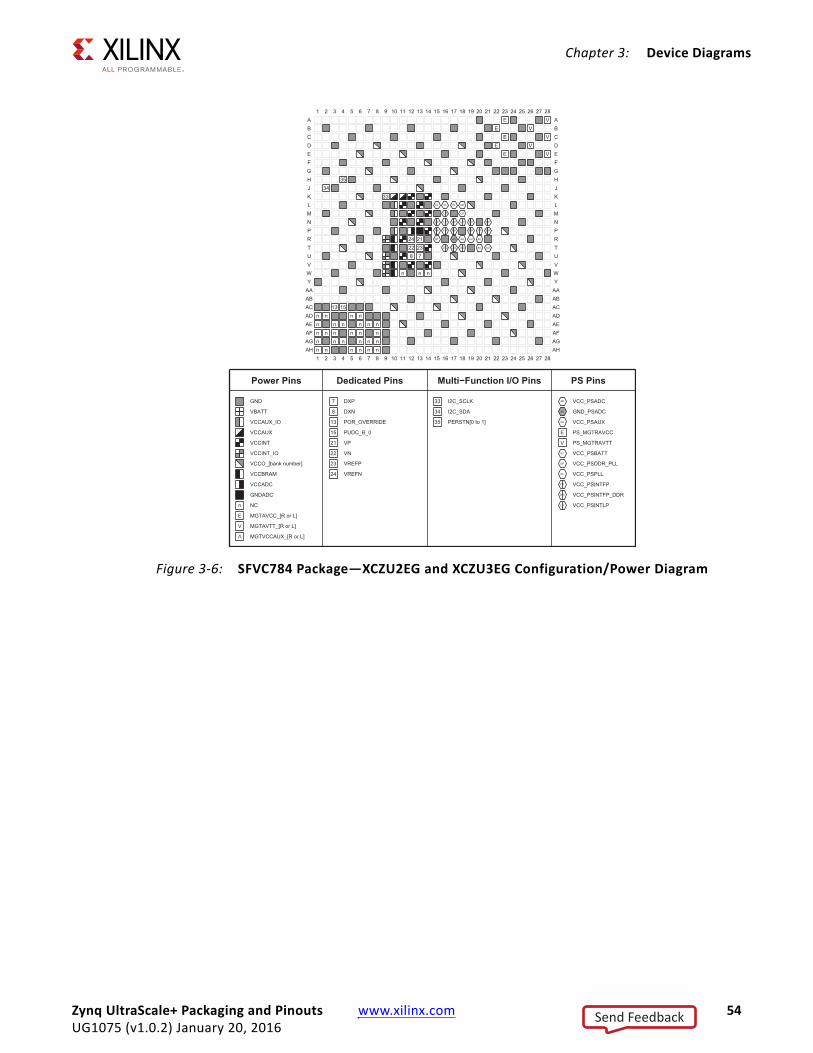
X-Ref Target - Figure 3-6
Figure 3-6: SFVC784 Package—XCZU2EG and XCZU3EG Configuration/Power Diagram
8 723
24 2122
1513
3534
33
n n n
nn n n
nn
n n nn n nn n n n nn n n n nn n n n n n
AD
EE
EE
E
VV
VV
V
AD AU AU
AU AU
BT
DP
DP
F P
F P F P F P F P F P F P
D D D D D D
L P
L P L P L P L P L P
PL PL PL
1
1
2
2
3
3
4
4
5
5
6
6
7
7
8
8
9
9
10
10
11
11
12
12
13
13
14
14
15
15
16
16
17
17
18
18
19
19
20
20
21
21
22
22
23
23
24
24
25
25
26
26
27
27
28
28
A AB BC CD DE EF FG GH HJ JK KL LM MN NP PR RT TU UV VW WY Y
AA AAAB ABAC ACAD ADAE AEAF AFAG AGAH AH
Power Pins
GND
VBATT
VCCAUX_IO
VCCAUX
VCCINT
VCCINT_IO
VCCO_[bank number]
VCCBRAM
VCCADC
GNDADC
n NC
E MGTAVCC_[R or L]
V MGTAVTT_[R or L]
V
MGTVCCAUX_[R or L]
Dedicated Pins
7 DXP
8 DXN
13 POR_OVERRIDE
15 PUDC_B_0
21 VP
22 VN
23 VREFP
24 VREFN
Multi−Function I/O Pins
33 I2C_SCLK
34 I2C_SDA
35 PERSTN[0 to 1]
PS Pins
AD VCC_PSADC
AD GND_PSADC
AU VCC_PSAUX
E PS_MGTRAVCC
V PS_MGTRAVTT
BT VCC_PSBATT
DP VCC_PSDDR_PLL
PL VCC_PSPLL
F P VCC_PSINTFP
D D VCC_PSINTFP_DDR
L P VCC_PSINTLP
Zynq UltraScale+ Packaging and Pinouts www.xilinx.com 54UG1075 (v1.0.2) January 20, 2016
Send Feedback
Chapter 3: Device Diagrams
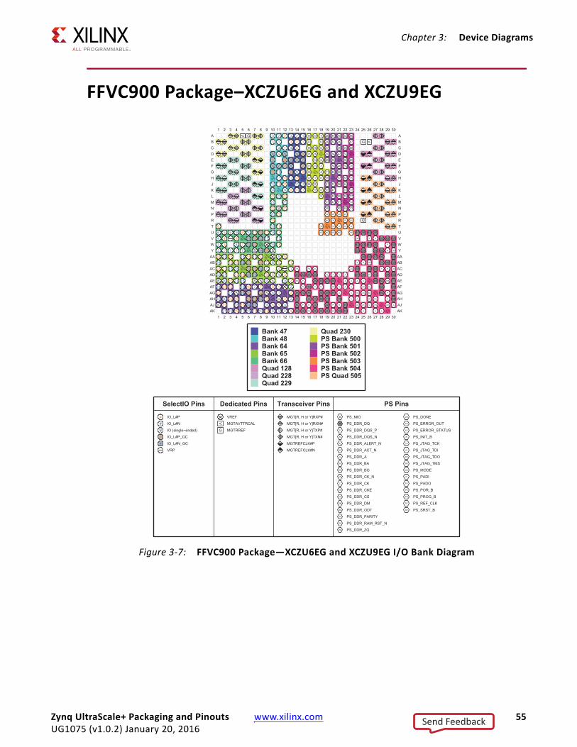
FFVC900 Package–XCZU6EG and XCZU9EGX-Ref Target - Figure 3-7
Figure 3-7: FFVC900 Package—XCZU6EG and XCZU9EG I/O Bank Diagram
12 1211
11
1010
9 9
88
7 7
66
55
44
33
2 21
1
12 121111
1010
9 988
77
6 65 5
4 4
33
22
11
2424 23 232222
2121
20 20
1919
S
S
1818
1717
16 161515
14 14
1313
12 1211 1110 109 9
88
77
S
66
554 43 32 2 1 1
2424 23 23
2222
2121
20 20
1919
S S
1818
1717
1616
15 15
1414
13 131212
1111
10 10
99
88
77
S
6 65 5
44
33
22
11
24 242323
2222
212120 20
19 19S
S
1818
1717
16 16
15 151414
13 131212
1111
10 1099
887 7
S
66
55
4 433 2
211
0128
1128
2128
3128
0
1
2
3
0128
1128
2128
3128
0
1
2
3
0128
0
1128
1
G
V
0228
1228
2228
3228
0
1
2
3
0228
1228
2228
3228
0
1
2
3
0228
0
1228
1
G
V
0229
1229
2229
3229
0
1
2
3
0229
1229
2229
3229
0
1
2
3
0229
0
1229
1
0230
1230
2230
3230
0
1
2
3
0230
1230
2230
3230
0
1
2
3
0230
0
1230
1
0
1
10
11
12
13
14
15
16
17
18
19
2
20
21
22
23
24
25
3
4
5
6
7
8
9
26
27
28
29
30
31
32
33
34
35
36
37
38
39
40
41
42
43
44 45
46
47
48
49
50
51
52
53
54
55
56
57
58
59
60
61
62
63
64
65
66
67
68
69
70
71
72
73
74
75
76 77
DN
EO ES
IN
CK
DIDO
MS
MD MD MD MD
PI PO
PR
PG
RCSR
A A
A
A
A
A
A A
AA
A
A
A
A
A AA A
AC
AL
BA
BA BG
BG
CN
CN
C
C
CE
CE
CS
CS
DM DM
DM
DM
DM
DM
DM
DM
DM
0
1
10
11
12 13
14
15
16 17 18
19
2
20 2122 23
24 25 2627
28
293
30 31
32 33
34 35
36
37 38
39
4
404142 43
44 454647
48
49
5
5051
52
53 54 55
5657
5859
6
60
6162 63
64
65
66
67
68
69
7
70
71
89
N N
N N
N
N
N
N
N
P P
P
P
P
P
P
P
P
OD
OD
PA RS ZQ
0505
1505
2505
3505
0
1
2
3
0505
1505
2505
3505
0
1
2
3
0505
0
1505
1
2505
2
3505
3
G
VCCO47VCCO47
VCCO48
VCCO48
VCCO64VCCO64
VCCO64
VCCO65
VCCO65VCCO65
VCCO66VCCO66
VCCO66
VCCO500
VCCO500
VCCO500
VCCO501
VCCO501
VCCO501
VCCO502
VCCO502
VCCO502
VCCO503VCCO503
VCCO504
VCCO504
VCCO504
VCCO504
VCCO504
VCCO504VCCO504
1
1
2
2
3
3
4
4
5
5
6
6
7
7
8
8
9
9
10
10
11
11
12
12
13
13
14
14
15
15
16
16
17
17
18
18
19
19
20
20
21
21
22
22
23
23
24
24
25
25
26
26
27
27
28
28
29
29
30
30
A AB BC CD DE EF FG GH HJ JK KL LM MN NP PR RT TU UV VW WY Y
AA AAAB ABAC ACAD ADAE AEAF AFAG AGAH AHAJ AJAK AK
SelectIO Pins
# IO_L#P
# IO_L#N
S IO (single−ended)
# IO_L#P_GC
# IO_L#N_GC
VRP
Dedicated Pins
VREF
V
MGTAVTTRCAL
G MGTRREF
Transceiver Pins# MGT[R, H or Y]RXP#
# MGT[R, H or Y]RXN## MGT[R, H or Y]TXP#
# MGT[R, H or Y]TXN## MGTREFCLK#P
# MGTREFCLK#N
PS Pins
# PS_MIO
# PS_DDR_DQP PS_DDR_DQS_PN PS_DDR_DQS_NAL PS_DDR_ALERT_NAC PS_DDR_ACT_NA PS_DDR_A
BA PS_DDR_BABG PS_DDR_BGCN PS_DDR_CK_NC PS_DDR_CK
CE PS_DDR_CKECS PS_DDR_CSDM PS_DDR_DMOD PS_DDR_ODTPA PS_DDR_PARITYRS PS_DDR_RAM_RST_NZQ PS_DDR_ZQ
DN PS_DONEEO PS_ERROR_OUTES PS_ERROR_STATUSIN PS_INIT_BCK PS_JTAG_TCKDI PS_JTAG_TDIDO PS_JTAG_TDOMS PS_JTAG_TMSMD PS_MODEPI PS_PADIPO PS_PADOPR PS_POR_BPG PS_PROG_BRC PS_REF_CLKSR PS_SRST_B
Bank 47Bank 48Bank 64Bank 65Bank 66Quad 128Quad 228Quad 229
Quad 230PS Bank 500PS Bank 501PS Bank 502PS Bank 503PS Bank 504PS Quad 505
Zynq UltraScale+ Packaging and Pinouts www.xilinx.com 55UG1075 (v1.0.2) January 20, 2016
Send Feedback
Chapter 3: Device Diagrams
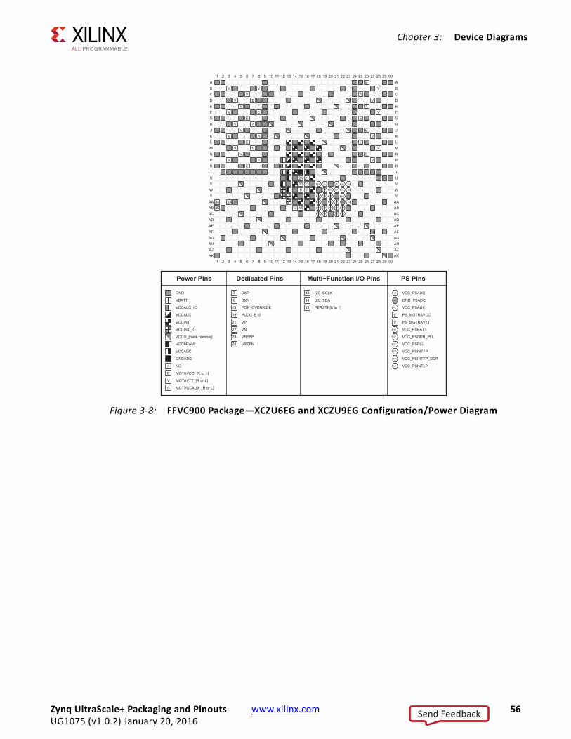
X-Ref Target - Figure 3-8
Figure 3-8: FFVC900 Package—XCZU6EG and XCZU9EG Configuration/Power Diagram
8 723
24 2122
15133534 33
AD
AD
AU
AU
AU
AU
E
E
E
V
V
V
BT
DP DP
F P
F P F P F P F P
F P F P
D D
D D D D
L P
L P L P L P
L P L P
PL PL PL
E
E
E
EE
EE
EE
V VV
VV
V
VV
V
VV
V
V
V
V
V
V
V
V
1
1
2
2
3
3
4
4
5
5
6
6
7
7
8
8
9
9
10
10
11
11
12
12
13
13
14
14
15
15
16
16
17
17
18
18
19
19
20
20
21
21
22
22
23
23
24
24
25
25
26
26
27
27
28
28
29
29
30
30
A AB BC CD DE EF FG GH HJ JK KL LM MN NP PR RT TU UV VW WY Y
AA AAAB ABAC ACAD ADAE AEAF AFAG AGAH AHAJ AJAK AK
Power Pins
GND
VBATT
VCCAUX_IO
VCCAUX
VCCINT
VCCINT_IO
VCCO_[bank number]
VCCBRAM
VCCADC
GNDADC
n NC
E MGTAVCC_[R or L]
V MGTAVTT_[R or L]
V
MGTVCCAUX_[R or L]
Dedicated Pins
7 DXP
8 DXN
13 POR_OVERRIDE
15 PUDC_B_0
21 VP
22 VN
23 VREFP
24 VREFN
Multi−Function I/O Pins
33 I2C_SCLK
34 I2C_SDA
35 PERSTN[0 to 1]
PS Pins
AD VCC_PSADC
AD GND_PSADC
AU VCC_PSAUX
E PS_MGTRAVCC
V PS_MGTRAVTT
BT VCC_PSBATT
DP VCC_PSDDR_PLL
PL VCC_PSPLL
F P VCC_PSINTFP
D D VCC_PSINTFP_DDR
L P VCC_PSINTLP
Zynq UltraScale+ Packaging and Pinouts www.xilinx.com 56UG1075 (v1.0.2) January 20, 2016
Send Feedback
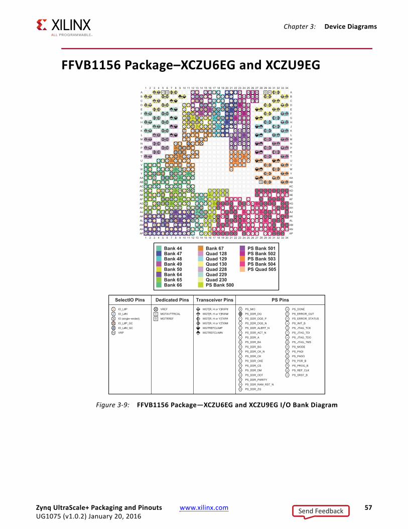
Chapter 3: Device Diagrams
FFVB1156 Package–XCZU6EG and XCZU9EGX-Ref Target - Figure 3-9
Figure 3-9: FFVB1156 Package—XCZU6EG and XCZU9EG I/O Bank Diagram
12 12
111110
10
9 9887
7
6 655
4 433221 1
1212
1111
1010
9 988
7766
55
44
3322
1 1
1212
11111010
99
8877
6655
44
33
22
11
1212
11111010 998
877
66
55
4433
22
11
12 12
1111
10 1099
8 87 7
66 5 5
44
33 2
2
11
2424
2323222221
21
20 20
1919
SS 181817
1716 16
1515
14 141313
1212
11 1110 10
9 988 7 7 S
665 5
443
3
22
1 124 2423 23
22 2221 21
2020
19 19S
S
18 1817 17
1616
15 15
141413 13
12 1211 11
10 10
9 9
88
7 7
S6 6
55
44
3 32 2
1 1
24 2423 23
2222
21 21
2020
1919
S
S1818
1717
16 16151514 14
1313
1212
1111 10
109 9
88
7 7 S
66
5 5 44 3
3
2 2
11
24 242323
22 22
2121
2020
1919
S
S
18 18
1717
1616
15 15
14 1413 13 12 12
11 11
1010
99
8 8
77
S66
55
4 4
33
22
11
0128
1128
2128
3128
0
1
2
3
0128
1128
2128
3128
0
1
2
3
1128
1
0128
0
G
V0
129
1129
2129
3129
0
1
2
3
0129
1129
2129
3129
0
1
2
3
1129
1
0129
0
0130
1130
2130
3130
0
1
2
3
0130
1130
2130
3130
0
1
2
3
0130
0
1130
1
0228
1228
2228
3228
0
1
2
3
0228
1228
2228
3228
0
1
2
3
1228
1
0228
0
G
V
0229
1229
2229
3229
0
1
2
3
0229
1229
2229
3229
0
1
2
3
1229
1
0229
0
0230
1230
2230
3230
0
1
2
3
0230
1230
2230
3230
0
1
2
3
0230
0
1230
1
0
1
2
3
4
5
6
7
8
9
10
11
12
13
14
15
16
17
18
19
20
21
2223
2425
26
27
28
29
30
31
32 33
34
35
36
37
38
39
40
41
42
43
44
45
46
47
48
49
50
51
52
53
54
55
56
57
58
59
60
61
62
63
64 65 66
67 68 69
70 71
72
73
74
75
76
77
DN
EO
ES
IN
CK
DI
DO
MS
MD
MD
MD
MD
PI PO PR
PG RCSR
A A
A
A
A
A
AA
A
A
A AA
A
AAAA
AC
AL
BA
BA
BG
BG
CN
CN
C
C
CE
CE
CS
CS
DM
DM
DM
DM DM
DM
DM
DM
DM
01 23
456
7
89 10
11
12 13
14
1516
17
18
19
20
21
2223 24
25
2627
28
29 30
31
32333435
36
37 38
39
40
41 42 43
4445 46 47
48
49
5051
5253
5455
56 57
58 59
60 61 6263
64
65 66 67
68 69 70
71
N N
N
N N
N
N
N
NP P
P P P
P
P
P
P
OD
OD
PA RS ZQ
0505
1505
2505
3505
0
1
2
3
0505
1505
2505
3505
0
1
2
3
0505
0
1505
1
2505
23
505
3
G
VCCO44
VCCO44
VCCO47
VCCO47
VCCO48
VCCO48
VCCO49VCCO49
VCCO50
VCCO50
VCCO64VCCO64
VCCO64
VCCO65
VCCO65VCCO65
VCCO66
VCCO66VCCO66
VCCO67
VCCO67VCCO67
VCCO500
VCCO500
VCCO500
VCCO501VCCO501
VCCO502
VCCO502VCCO502
VCCO503VCCO503
VCCO504
VCCO504
VCCO504
VCCO504
VCCO504
VCCO504
VCCO504
1
1
2
2
3
3
4
4
5
5
6
6
7
7
8
8
9
9
10
10
11
11
12
12
13
13
14
14
15
15
16
16
17
17
18
18
19
19
20
20
21
21
22
22
23
23
24
24
25
25
26
26
27
27
28
28
29
29
30
30
31
31
32
32
33
33
34
34
A AB BC CD DE EF FG GH HJ JK KL LM MN NP PR RT TU UV VW WY Y
AA AAAB ABAC ACAD ADAE AEAF AFAG AGAH AHAJ AJAK AKAL ALAM AMAN ANAP AP
Bank 44Bank 47Bank 48Bank 49Bank 50Bank 64Bank 65Bank 66
Bank 67Quad 128Quad 129Quad 130Quad 228Quad 229Quad 230PS Bank 500
PS Bank 501PS Bank 502PS Bank 503PS Bank 504PS Quad 505
SelectIO Pins
# IO_L#P
# IO_L#N
S IO (single−ended)
# IO_L#P_GC
# IO_L#N_GC
VRP
Dedicated Pins
VREF
V
MGTAVTTRCAL
G MGTRREF
Transceiver Pins# MGT[R, H or Y]RXP#
# MGT[R, H or Y]RXN## MGT[R, H or Y]TXP#
# MGT[R, H or Y]TXN## MGTREFCLK#P
# MGTREFCLK#N
PS Pins
# PS_MIO
# PS_DDR_DQP PS_DDR_DQS_PN PS_DDR_DQS_NAL PS_DDR_ALERT_NAC PS_DDR_ACT_NA PS_DDR_A
BA PS_DDR_BABG PS_DDR_BGCN PS_DDR_CK_NC PS_DDR_CK
CE PS_DDR_CKECS PS_DDR_CSDM PS_DDR_DMOD PS_DDR_ODTPA PS_DDR_PARITYRS PS_DDR_RAM_RST_NZQ PS_DDR_ZQ
DN PS_DONEEO PS_ERROR_OUTES PS_ERROR_STATUSIN PS_INIT_BCK PS_JTAG_TCKDI PS_JTAG_TDIDO PS_JTAG_TDOMS PS_JTAG_TMSMD PS_MODEPI PS_PADIPO PS_PADOPR PS_POR_BPG PS_PROG_BRC PS_REF_CLKSR PS_SRST_B
Zynq UltraScale+ Packaging and Pinouts www.xilinx.com 57UG1075 (v1.0.2) January 20, 2016
Send Feedback
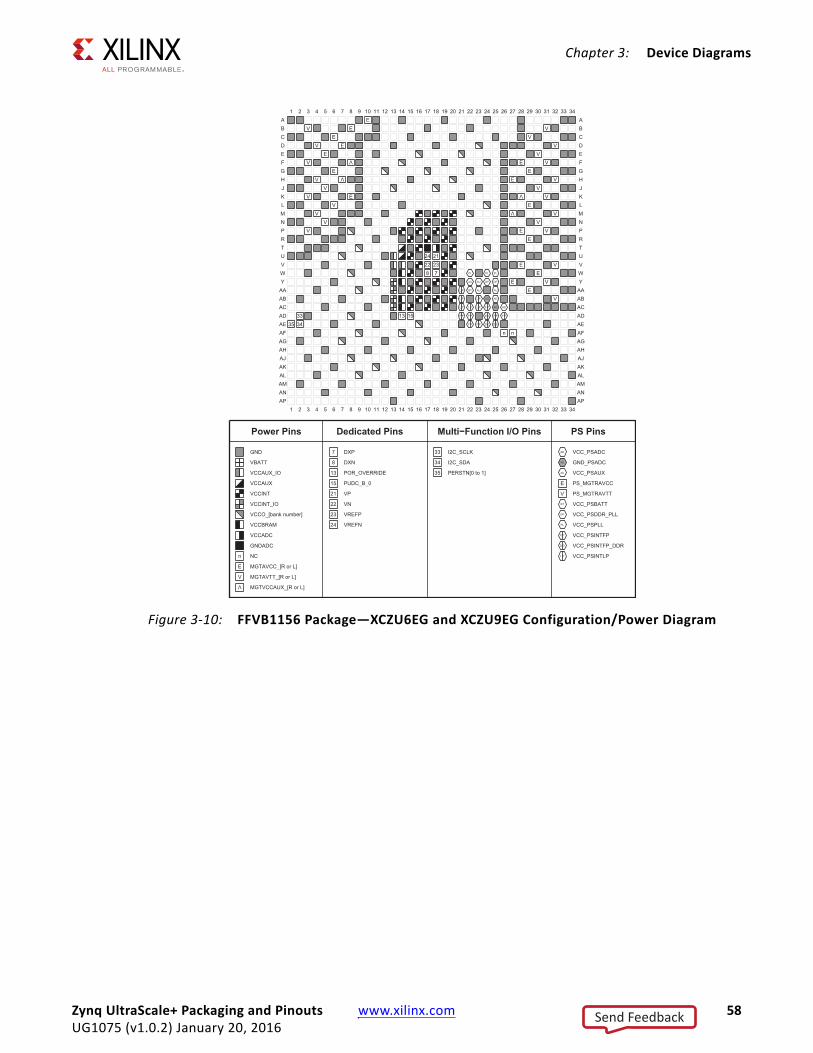
Chapter 3: Device Diagrams
X-Ref Target - Figure 3-10
Figure 3-10: FFVB1156 Package—XCZU6EG and XCZU9EG Configuration/Power Diagram
Power Pins
GND
VBATT
VCCAUX_IO
VCCAUX
VCCINT
VCCINT_IO
VCCO_[bank number]
VCCBRAM
VCCADC
GNDADC
n NC
E MGTAVCC_[R or L]
V MGTAVTT_[R or L]
V
MGTVCCAUX_[R or L]
Dedicated Pins
7 DXP
8 DXN
13 POR_OVERRIDE
15 PUDC_B_0
21 VP
22 VN
23 VREFP
24 VREFN
Multi−Function I/O Pins
33 I2C_SCLK
34 I2C_SDA
35 PERSTN[0 to 1]
PS Pins
AD VCC_PSADC
AD GND_PSADC
AU VCC_PSAUX
E PS_MGTRAVCC
V PS_MGTRAVTT
BT VCC_PSBATT
DP VCC_PSDDR_PLL
PL VCC_PSPLL
F P VCC_PSINTFP
D D VCC_PSINTFP_DDR
L P VCC_PSINTLP
8 723
24 2122
151335 34
33
AD
AD
AD
AD
AU AU
AU AU
EE
E
E
EE
EE
EE
E
E
E
VV
VV
V
VV
V
VV
V
V
V
V
VV
VV
VV
V
V
V
V
V
E
EE
E
V
V
VBT
DP DP
F P
F P F P F P F P
F P F P
D D
D D D D
L P
L P L P
L P L P L P
PL PL PL
nn
1
1
2
2
3
3
4
4
5
5
6
6
7
7
8
8
9
9
10
10
11
11
12
12
13
13
14
14
15
15
16
16
17
17
18
18
19
19
20
20
21
21
22
22
23
23
24
24
25
25
26
26
27
27
28
28
29
29
30
30
31
31
32
32
33
33
34
34
A AB BC CD DE EF FG GH HJ JK KL LM MN NP PR RT TU UV VW WY Y
AA AAAB ABAC ACAD ADAE AEAF AFAG AGAH AHAJ AJAK AKAL ALAM AMAN ANAP AP
Zynq UltraScale+ Packaging and Pinouts www.xilinx.com 58UG1075 (v1.0.2) January 20, 2016
Send Feedback
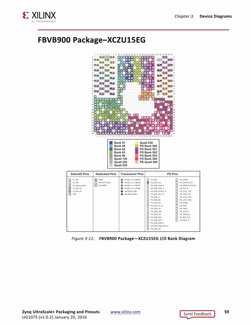
Chapter 3: Device Diagrams
FBVB900 Package–XCZU15EGX-Ref Target - Figure 3-11
Figure 3-11: FBVB900 Package—XCZU15EG I/O Bank Diagram
12 1211
11
1010
9 9
88
7 7
66
55
44
33
2 21
1
12 121111
1010
9 988
77
6 65 5
4 4
33
22
11
2424 23 232222
2121
20 20
1919
S
S
1818
1717
16 161515
14 14
1313
12 1211 1110 109 9
88
77
S
66
554 43 32 2 1 1
2424 23 23
2222
2121
20 20
1919
S S
1818
1717
1616
15 15
1414
13 131212
1111
10 10
99
88
77
S
6 65 5
44
33
22
11
24 242323
2222
212120 20
19 19S
S
1818
1717
16 16
15 151414
13 131212
1111
10 1099
887 7
S
66
55
4 433 2
211
0128
1128
2128
3128
0
1
2
3
0128
1128
2128
3128
0
1
2
3
0128
0
1128
1
G
V
0228
1228
2228
3228
0
1
2
3
0228
1228
2228
3228
0
1
2
3
0228
0
1228
1
G
V
0229
1229
2229
3229
0
1
2
3
0229
1229
2229
3229
0
1
2
3
0229
0
1229
1
0230
1230
2230
3230
0
1
2
3
0230
1230
2230
3230
0
1
2
3
0230
0
1230
1
0
1
10
11
12
13
14
15
16
17
18
19
2
20
21
22
23
24
25
3
4
5
6
7
8
9
26
27
28
29
30
31
32
33
34
35
36
37
38
39
40
41
42
43
44 45
46
47
48
49
50
51
52
53
54
55
56
57
58
59
60
61
62
63
64
65
66
67
68
69
70
71
72
73
74
75
76 77
DN
EO ES
IN
CK
DIDO
MS
MD MD MD MD
PI PO
PR
PG
RCSR
A A
A
A
A
A
A A
AA
A
A
A
A
A AA A
AC
AL
BA
BA BG
BG
CN
CN
C
C
CE
CE
CS
CS
DM DM
DM
DM
DM
DM
DM
DM
DM
0
1
10
11
12 13
14
15
16 17 18
19
2
20 2122 23
24 25 2627
28
293
30 31
32 33
34 35
36
37 38
39
4
404142 43
44 454647
48
49
5
5051
52
53 54 55
5657
5859
6
60
6162 63
64
65
66
67
68
69
7
70
71
89
N N
N N
N
N
N
N
N
P P
P
P
P
P
P
P
P
OD
OD
PA RS ZQ
0505
1505
2505
3505
0
1
2
3
0505
1505
2505
3505
0
1
2
3
0505
0
1505
1
2505
2
3505
3
G
VCCO47VCCO47
VCCO48
VCCO48
VCCO64VCCO64
VCCO64
VCCO65
VCCO65VCCO65
VCCO66VCCO66
VCCO66
VCCO500
VCCO500
VCCO500
VCCO501
VCCO501
VCCO501
VCCO502
VCCO502
VCCO502
VCCO503VCCO503
VCCO504
VCCO504
VCCO504
VCCO504
VCCO504
VCCO504VCCO504
1
1
2
2
3
3
4
4
5
5
6
6
7
7
8
8
9
9
10
10
11
11
12
12
13
13
14
14
15
15
16
16
17
17
18
18
19
19
20
20
21
21
22
22
23
23
24
24
25
25
26
26
27
27
28
28
29
29
30
30
A AB BC CD DE EF FG GH HJ JK KL LM MN NP PR RT TU UV VW WY Y
AA AAAB ABAC ACAD ADAE AEAF AFAG AGAH AHAJ AJAK AK
Bank 47Bank 48Bank 64Bank 65Bank 66Quad 128Quad 228Quad 229
Quad 230PS Bank 500PS Bank 501PS Bank 502PS Bank 503PS Bank 504PS Quad 505
SelectIO Pins
# IO_L#P
# IO_L#N
S IO (single−ended)
# IO_L#P_GC
# IO_L#N_GC
VRP
Dedicated Pins
VREF
V
MGTAVTTRCAL
G MGTRREF
Transceiver Pins# MGT[R, H or Y]RXP#
# MGT[R, H or Y]RXN## MGT[R, H or Y]TXP#
# MGT[R, H or Y]TXN## MGTREFCLK#P
# MGTREFCLK#N
PS Pins
# PS_MIO
# PS_DDR_DQP PS_DDR_DQS_PN PS_DDR_DQS_NAL PS_DDR_ALERT_NAC PS_DDR_ACT_NA PS_DDR_A
BA PS_DDR_BABG PS_DDR_BGCN PS_DDR_CK_NC PS_DDR_CK
CE PS_DDR_CKECS PS_DDR_CSDM PS_DDR_DMOD PS_DDR_ODTPA PS_DDR_PARITYRS PS_DDR_RAM_RST_NZQ PS_DDR_ZQ
DN PS_DONEEO PS_ERROR_OUTES PS_ERROR_STATUSIN PS_INIT_BCK PS_JTAG_TCKDI PS_JTAG_TDIDO PS_JTAG_TDOMS PS_JTAG_TMSMD PS_MODEPI PS_PADIPO PS_PADOPR PS_POR_BPG PS_PROG_BRC PS_REF_CLKSR PS_SRST_B
Zynq UltraScale+ Packaging and Pinouts www.xilinx.com 59UG1075 (v1.0.2) January 20, 2016
Send Feedback
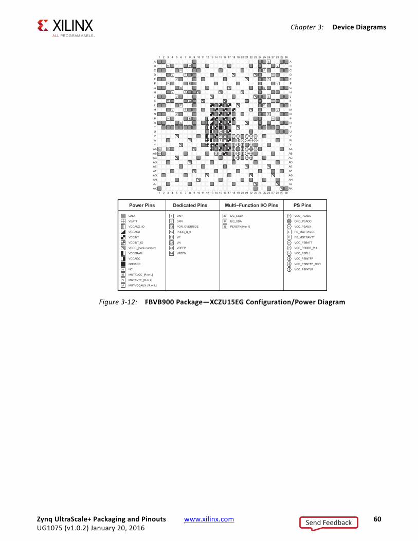
Chapter 3: Device Diagrams
X-Ref Target - Figure 3-12
Figure 3-12: FBVB900 Package—XCZU15EG Configuration/Power Diagram
8 723
24 2122
15133534 33
AD
AD
AU
AU
AU
AU
E
E
E
V
V
V
BT
DP DP
F P
F P F P F P F P
F P F P
D D
D D D D
L P
L P L P L P
L P L P
PL PL PL
E
E
E
EE
EE
EE
V VV
VV
V
VV
V
VV
V
V
V
V
V
V
V
V
1
1
2
2
3
3
4
4
5
5
6
6
7
7
8
8
9
9
10
10
11
11
12
12
13
13
14
14
15
15
16
16
17
17
18
18
19
19
20
20
21
21
22
22
23
23
24
24
25
25
26
26
27
27
28
28
29
29
30
30
A AB BC CD DE EF FG GH HJ JK KL LM MN NP PR RT TU UV VW WY Y
AA AAAB ABAC ACAD ADAE AEAF AFAG AGAH AHAJ AJAK AK
Power Pins
GND
VBATT
VCCAUX_IO
VCCAUX
VCCINT
VCCINT_IO
VCCO_[bank number]
VCCBRAM
VCCADC
GNDADC
n NC
E MGTAVCC_[R or L]
V MGTAVTT_[R or L]
V
MGTVCCAUX_[R or L]
Dedicated Pins
7 DXP
8 DXN
13 POR_OVERRIDE
15 PUDC_B_0
21 VP
22 VN
23 VREFP
24 VREFN
Multi−Function I/O Pins
33 I2C_SCLK
34 I2C_SDA
35 PERSTN[0 to 1]
PS Pins
AD VCC_PSADC
AD GND_PSADC
AU VCC_PSAUX
E PS_MGTRAVCC
V PS_MGTRAVTT
BT VCC_PSBATT
DP VCC_PSDDR_PLL
PL VCC_PSPLL
F P VCC_PSINTFP
D D VCC_PSINTFP_DDR
L P VCC_PSINTLP
Zynq UltraScale+ Packaging and Pinouts www.xilinx.com 60UG1075 (v1.0.2) January 20, 2016
Send Feedback
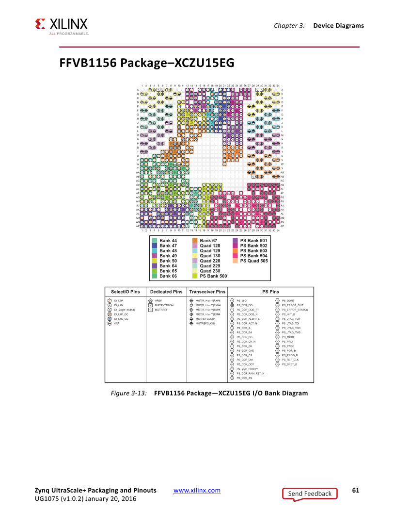
Chapter 3: Device Diagrams
FFVB1156 Package–XCZU15EGX-Ref Target - Figure 3-13
Figure 3-13: FFVB1156 Package—XCZU15EG I/O Bank Diagram
12 12
111110
10
9 9887
7
6 655
4 433221 1
1212
1111
1010
9 988
7766
55
44
3322
1 1
1212
11111010
99
8877
6655
44
33
22
11
1212
11111010 998
877
66
55
4433
22
11
12 12
1111
10 1099
8 87 7
66 5 5
44
33 2
2
11
2424
2323222221
21
20 20
1919
SS 181817
1716 16
1515
14 141313
1212
11 1110 10
9 988 7 7 S
665 5
443
3
22
1 124 2423 23
22 2221 21
2020
19 19S
S
18 1817 17
1616
15 15
141413 13
12 1211 11
10 10
9 9
88
7 7
S6 6
55
44
3 32 2
1 1
24 2423 23
2222
21 21
2020
1919
S
S1818
1717
16 16151514 14
1313
1212
1111 10
109 9
88
7 7 S
66
5 5 44 3
3
2 2
11
24 242323
22 22
2121
2020
1919
S
S
18 18
1717
1616
15 15
14 1413 13 12 12
11 11
1010
99
8 8
77
S66
55
4 4
33
22
11
0128
1128
2128
3128
0
1
2
3
0128
1128
2128
3128
0
1
2
3
1128
1
0128
0
G
V0
129
1129
2129
3129
0
1
2
3
0129
1129
2129
3129
0
1
2
3
1129
1
0129
0
0130
1130
2130
3130
0
1
2
3
0130
1130
2130
3130
0
1
2
3
0130
0
1130
1
0228
1228
2228
3228
0
1
2
3
0228
1228
2228
3228
0
1
2
3
1228
1
0228
0
G
V
0229
1229
2229
3229
0
1
2
3
0229
1229
2229
3229
0
1
2
3
1229
1
0229
0
0230
1230
2230
3230
0
1
2
3
0230
1230
2230
3230
0
1
2
3
0230
0
1230
1
0
1
2
3
4
5
6
7
8
9
10
11
12
13
14
15
16
17
18
19
20
21
2223
2425
26
27
28
29
30
31
32 33
34
35
36
37
38
39
40
41
42
43
44
45
46
47
48
49
50
51
52
53
54
55
56
57
58
59
60
61
62
63
64 65 66
67 68 69
70 71
72
73
74
75
76
77
DN
EO
ES
IN
CK
DI
DO
MS
MD
MD
MD
MD
PI PO PR
PG RCSR
A A
A
A
A
A
AA
A
A
A AA
A
AAAA
AC
AL
BA
BA
BG
BG
CN
CN
C
C
CE
CE
CS
CS
DM
DM
DM
DM DM
DM
DM
DM
DM
01 23
456
7
89 10
11
12 13
14
1516
17
18
19
20
21
2223 24
25
2627
28
29 30
31
32333435
36
37 38
39
40
41 42 43
4445 46 47
48
49
5051
5253
5455
56 57
58 59
60 61 6263
64
65 66 67
68 69 70
71
N N
N
N N
N
N
N
NP P
P P P
P
P
P
P
OD
OD
PA RS ZQ
0505
1505
2505
3505
0
1
2
3
0505
1505
2505
3505
0
1
2
3
0505
0
1505
1
2505
23
505
3
G
VCCO44
VCCO44
VCCO47
VCCO47
VCCO48
VCCO48
VCCO49VCCO49
VCCO50
VCCO50
VCCO64VCCO64
VCCO64
VCCO65
VCCO65VCCO65
VCCO66
VCCO66VCCO66
VCCO67
VCCO67VCCO67
VCCO500
VCCO500
VCCO500
VCCO501VCCO501
VCCO502
VCCO502VCCO502
VCCO503VCCO503
VCCO504
VCCO504
VCCO504
VCCO504
VCCO504
VCCO504
VCCO504
1
1
2
2
3
3
4
4
5
5
6
6
7
7
8
8
9
9
10
10
11
11
12
12
13
13
14
14
15
15
16
16
17
17
18
18
19
19
20
20
21
21
22
22
23
23
24
24
25
25
26
26
27
27
28
28
29
29
30
30
31
31
32
32
33
33
34
34
A AB BC CD DE EF FG GH HJ JK KL LM MN NP PR RT TU UV VW WY Y
AA AAAB ABAC ACAD ADAE AEAF AFAG AGAH AHAJ AJAK AKAL ALAM AMAN ANAP AP
Bank 44Bank 47Bank 48Bank 49Bank 50Bank 64Bank 65Bank 66
Bank 67Quad 128Quad 129Quad 130Quad 228Quad 229Quad 230PS Bank 500
PS Bank 501PS Bank 502PS Bank 503PS Bank 504PS Quad 505
SelectIO Pins
# IO_L#P
# IO_L#N
S IO (single−ended)
# IO_L#P_GC
# IO_L#N_GC
VRP
Dedicated Pins
VREF
V
MGTAVTTRCAL
G MGTRREF
Transceiver Pins# MGT[R, H or Y]RXP#
# MGT[R, H or Y]RXN## MGT[R, H or Y]TXP#
# MGT[R, H or Y]TXN## MGTREFCLK#P
# MGTREFCLK#N
PS Pins
# PS_MIO
# PS_DDR_DQP PS_DDR_DQS_PN PS_DDR_DQS_NAL PS_DDR_ALERT_NAC PS_DDR_ACT_NA PS_DDR_A
BA PS_DDR_BABG PS_DDR_BGCN PS_DDR_CK_NC PS_DDR_CK
CE PS_DDR_CKECS PS_DDR_CSDM PS_DDR_DMOD PS_DDR_ODTPA PS_DDR_PARITYRS PS_DDR_RAM_RST_NZQ PS_DDR_ZQ
DN PS_DONEEO PS_ERROR_OUTES PS_ERROR_STATUSIN PS_INIT_BCK PS_JTAG_TCKDI PS_JTAG_TDIDO PS_JTAG_TDOMS PS_JTAG_TMSMD PS_MODEPI PS_PADIPO PS_PADOPR PS_POR_BPG PS_PROG_BRC PS_REF_CLKSR PS_SRST_B
Zynq UltraScale+ Packaging and Pinouts www.xilinx.com 61UG1075 (v1.0.2) January 20, 2016
Send Feedback

Chapter 3: Device Diagrams
X-Ref Target - Figure 3-14
Figure 3-14: FFVB1156 Package—XCZU15EG Configuration/Power Diagram
8 723
24 2122
151335 34
33
AD
AD
AD
AD
AU AU
AU AU
EE
E
E
EE
EE
EE
E
E
E
VV
VV
V
VV
V
VV
V
V
V
V
VV
VV
VV
V
V
V
V
V
E
EE
E
V
V
VBT
DP DP
F P
F P F P F P F P
F P F P
D D
D D D D
L P
L P L P
L P L P L P
PL PL PL
nn
1
1
2
2
3
3
4
4
5
5
6
6
7
7
8
8
9
9
10
10
11
11
12
12
13
13
14
14
15
15
16
16
17
17
18
18
19
19
20
20
21
21
22
22
23
23
24
24
25
25
26
26
27
27
28
28
29
29
30
30
31
31
32
32
33
33
34
34
A AB BC CD DE EF FG GH HJ JK KL LM MN NP PR RT TU UV VW WY Y
AA AAAB ABAC ACAD ADAE AEAF AFAG AGAH AHAJ AJAK AKAL ALAM AMAN ANAP AP
Power Pins
GND
VBATT
VCCAUX_IO
VCCAUX
VCCINT
VCCINT_IO
VCCO_[bank number]
VCCBRAM
VCCADC
GNDADC
n NC
E MGTAVCC_[R or L]
V MGTAVTT_[R or L]
V
MGTVCCAUX_[R or L]
Dedicated Pins
7 DXP
8 DXN
13 POR_OVERRIDE
15 PUDC_B_0
21 VP
22 VN
23 VREFP
24 VREFN
Multi−Function I/O Pins
33 I2C_SCLK
34 I2C_SDA
35 PERSTN[0 to 1]
PS Pins
AD VCC_PSADC
AD GND_PSADC
AU VCC_PSAUX
E PS_MGTRAVCC
V PS_MGTRAVTT
BT VCC_PSBATT
DP VCC_PSDDR_PLL
PL VCC_PSPLL
F P VCC_PSINTFP
D D VCC_PSINTFP_DDR
L P VCC_PSINTLP
Zynq UltraScale+ Packaging and Pinouts www.xilinx.com 62UG1075 (v1.0.2) January 20, 2016
Send Feedback
Chapter 4
Mechanical Drawings
SummaryThis chapter provides mechanical drawings (package specifications) of the Zynq UltraScale+ MPSoC packages. Table 4-1 is a cross-reference to the mechanical drawings by device and package combination.
Table 4-1: Cross-Reference to Mechanical Drawings by Package
PackageDevice
XCZU2EG XCZU3EG XCZU4EV XCZU5EV XCZU6EG XCZU7EV XCZU9EG XCZU11EG XCZU15EG XCZU17EG XCZU19EG
SBVA484
SFVA625
SFVC784
FBVB900
FFVC900 Figure 4-1 Figure 4-1 Figure 4-1
FFVB1156 Figure 4-2 Figure 4-2 Figure 4-2
FFVC1156
FFVB1517
FFVF1517
FFVC1760
FFVD1760
FFVE1924
Zynq UltraScale+ Packaging and Pinouts www.xilinx.com 63UG1075 (v1.0.2) January 20, 2016
Send Feedback
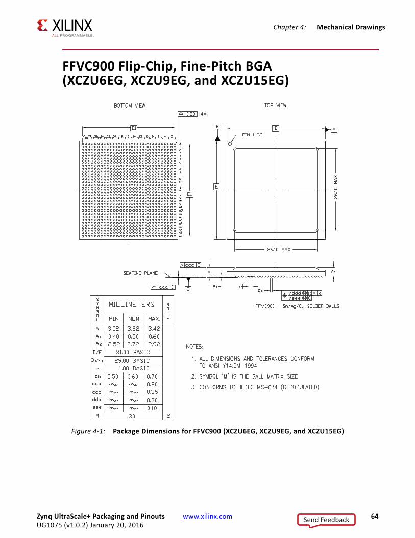
Chapter 4: Mechanical Drawings
FFVC900 Flip-Chip, Fine-Pitch BGA (XCZU6EG, XCZU9EG, and XCZU15EG)
X-Ref Target - Figure 4-1
Figure 4-1: Package Dimensions for FFVC900 (XCZU6EG, XCZU9EG, and XCZU15EG)
Zynq UltraScale+ Packaging and Pinouts www.xilinx.com 64UG1075 (v1.0.2) January 20, 2016
Send Feedback
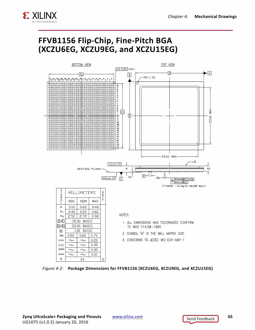
Chapter 4: Mechanical Drawings
FFVB1156 Flip-Chip, Fine-Pitch BGA (XCZU6EG, XCZU9EG, and XCZU15EG)
X-Ref Target - Figure 4-2
Figure 4-2: Package Dimensions for FFVB1156 (XCZU6EG, XCZU9EG, and XCZU15EG)
Zynq UltraScale+ Packaging and Pinouts www.xilinx.com 65UG1075 (v1.0.2) January 20, 2016
Send Feedback
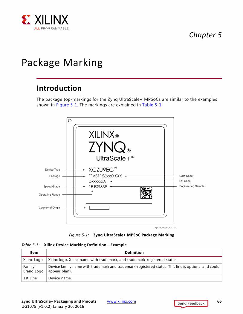
Chapter 5
Package Marking
IntroductionThe package top-markings for the Zynq UltraScale+ MPSoCs are similar to the examples shown in Figure 5-1. The markings are explained in Table 5-1.
X-Ref Target - Figure 5-1
Figure 5-1: Zynq UltraScale+ MPSoC Package Marking
XILINX®
ZYNQ®UltraScale+ TM
XCZU9EGTM
FFVB1156xxxXXXXDxxxxxxA1E ES9839
ug1075_c5_01_101315
Device Type
Package
Speed Grade
Operating Range
Country of Origin
Engineering Sample
Lot Code
Date Code
Table 5-1: Xilinx Device Marking Definition—Example
Item Definition
Xilinx Logo Xilinx logo, Xilinx name with trademark, and trademark-registered status.
Family Brand Logo
Device family name with trademark and trademark-registered status. This line is optional and could appear blank.
1st Line Device name.
Zynq UltraScale+ Packaging and Pinouts www.xilinx.com 66UG1075 (v1.0.2) January 20, 2016
Send Feedback
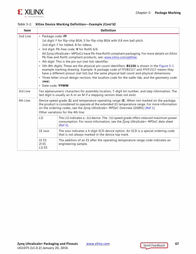
Chapter 5: Package Marking
2nd Line • Package code: FF1st digit: F for flip-chip BGA, S for flip-chip BGA with 0.8 mm ball pitch.2nd digit: F for lidded, B for lidless.
• 3rd digit: Pb-free code: V for RoHS 6/6.All Zynq UltraScale+ MPSoCs have Pb-free RoHS compliant packaging. For more details on Xilinx Pb-free and RoHS compliant products, see: www.xilinx.com/pbfree.
• 4th digit: This is the pin out (net list) identifier.• 5th–8th digits: These are the physical pin count identifiers: B1156 is shown in the Figure 5-1
example marking drawing. Example: A package code of FFVB1517 and FFVF1517 means they have a different pinout (net list) but the same physical ball count and physical dimensions.
• Three letter circuit design revision, the location code for the wafer fab, and the geometry code (xxx).
• Date code: YYWW
3rd Line Ten alphanumeric characters for assembly location, 7-digit lot number, and step information. The last digit is usually an A or an M if a stepping version does not exist.
4th Line Device speed grade (1) and temperature operating range (E). When not marked on the package, the product is considered to operate at the extended (E) temperature range. For more information on the ordering codes, see the Zynq UltraScale+ MPSoC Overview (DS891) [Ref 1].Other variations for the 4th line:
L1I The L1I indicates a -1LI device. The -1LI speed grade offers reduced maximum power consumption. For more information, see the Zynq UltraScale+ MPSoC data sheet [Ref 5].
1E xxxx The xxxx indicates a 4-digit SCD device option. An SCD is a special ordering code that is not always marked in the device top mark.
1E ES2I ESL1I ES
The addition of an ES after the operating temperature range code indicates an engineering sample.
Table 5-1: Xilinx Device Marking Definition—Example (Cont’d)
Item Definition
Zynq UltraScale+ Packaging and Pinouts www.xilinx.com 67UG1075 (v1.0.2) January 20, 2016
Send Feedback
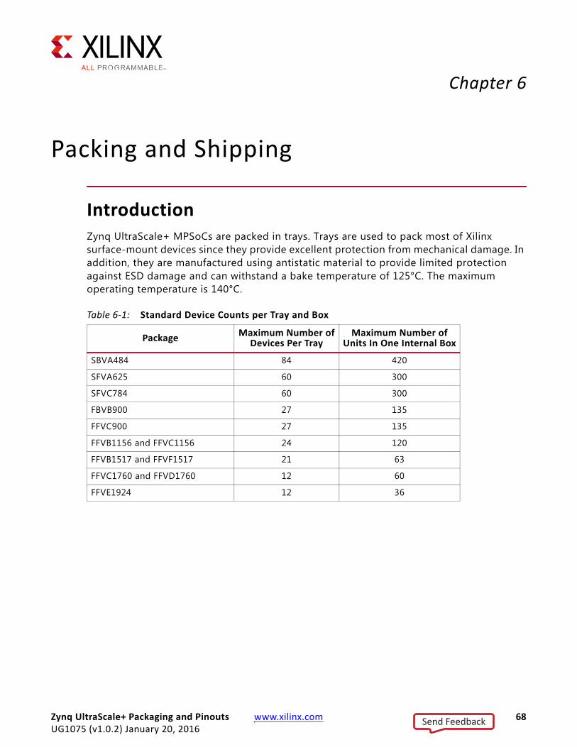
Zynq UltraScale+ Packaging and Pinouts www.xilinx.com 68UG1075 (v1.0.2) January 20, 2016
Chapter 6
Packing and Shipping
IntroductionZynq UltraScale+ MPSoCs are packed in trays. Trays are used to pack most of Xilinx surface-mount devices since they provide excellent protection from mechanical damage. In addition, they are manufactured using antistatic material to provide limited protection against ESD damage and can withstand a bake temperature of 125°C. The maximum operating temperature is 140°C.
Table 6-1: Standard Device Counts per Tray and Box
Package Maximum Number of Devices Per Tray
Maximum Number of Units In One Internal Box
SBVA484 84 420
SFVA625 60 300
SFVC784 60 300
FBVB900 27 135
FFVC900 27 135
FFVB1156 and FFVC1156 24 120
FFVB1517 and FFVF1517 21 63
FFVC1760 and FFVD1760 12 60
FFVE1924 12 36
Send Feedback
Chapter 7
Soldering Guidelines
Soldering GuidelinesTo implement and control the production of surface-mount assemblies, the dynamics of the Pb-free solder reflow process and how each element of the process is related to the end result must be thoroughly understood.
RECOMMENDED: Xilinx recommends that customers qualify their custom PCB assembly processes using package samples.
The primary phases of the Pb-free reflow process are:
• Melting the particles in the solder paste
• Wetting the surfaces to be joined
• Solidifying the solder into a strong metallurgical bond
The peak reflow temperature of a plastic surface-mount component (PSMC) body should not be more than 250°C maximum (260°C for dry rework only) for Pb-free packages (220°C for eutectic packages), and is package size dependent. For multiple BGAs in a single board and because of surrounding component differences, Xilinx recommends checking all BGA sites for varying temperatures.
The infrared reflow (IR) process is strongly dependent on equipment and loading. Components might overheat due to lack of thermal constraints. Unbalanced loading can lead to significant temperature variation on the board. These guidelines are intended to assist users in avoiding damage to the components; the actual profile should be determined by those using these guidelines. For complete information on package moisture / reflow classification and package reflow conditions, refer to the Joint IPC/JEDEC Standard J-STD-020C.
Pb-Free Reflow SolderingXilinx uses SnAgCu solder balls for BGA packages. In addition, suitable material are qualified for the higher reflow temperatures (250°C maximum, 260°C for dry rework only) required by Pb-free soldering processes.
Zynq UltraScale+ Packaging and Pinouts www.xilinx.com 69UG1075 (v1.0.2) January 20, 2016
Send Feedback
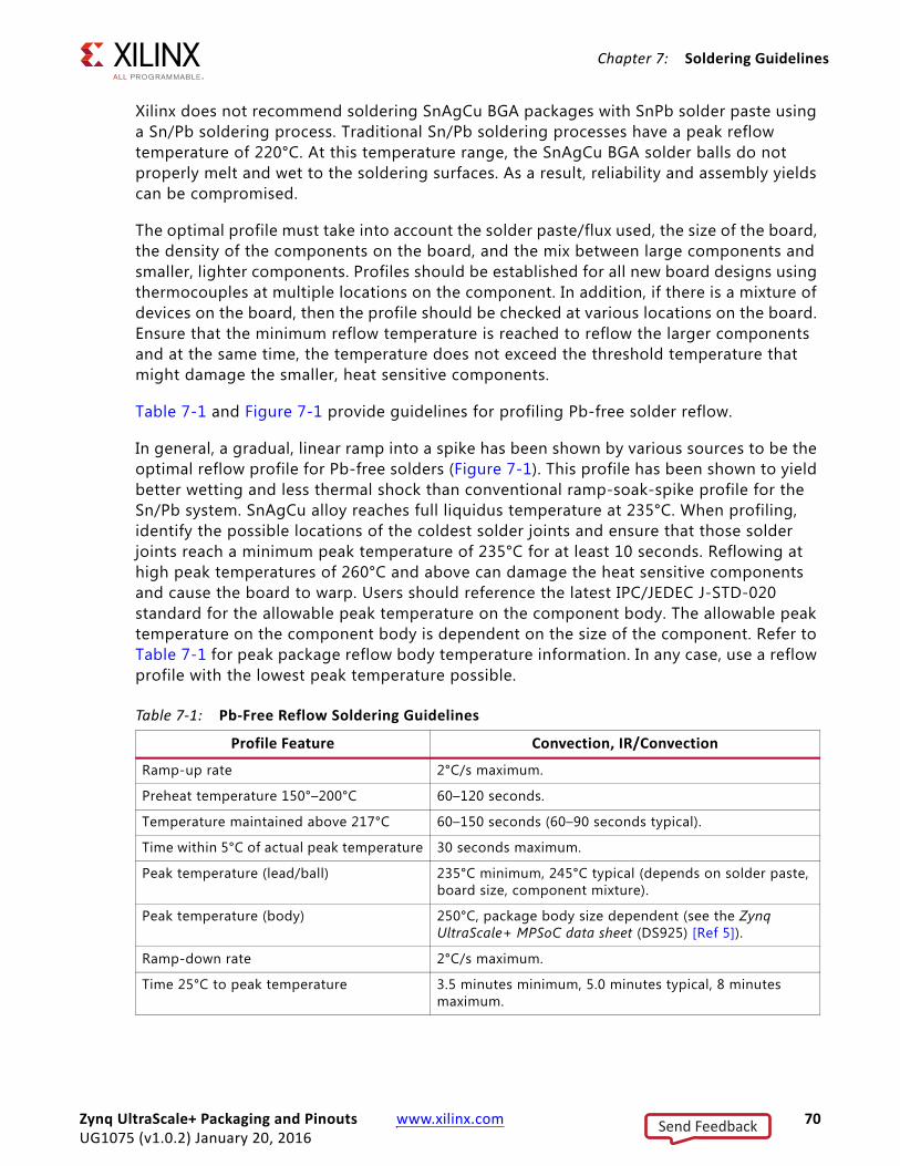
Chapter 7: Soldering Guidelines
Xilinx does not recommend soldering SnAgCu BGA packages with SnPb solder paste using a Sn/Pb soldering process. Traditional Sn/Pb soldering processes have a peak reflow temperature of 220°C. At this temperature range, the SnAgCu BGA solder balls do not properly melt and wet to the soldering surfaces. As a result, reliability and assembly yields can be compromised.
The optimal profile must take into account the solder paste/flux used, the size of the board, the density of the components on the board, and the mix between large components and smaller, lighter components. Profiles should be established for all new board designs using thermocouples at multiple locations on the component. In addition, if there is a mixture of devices on the board, then the profile should be checked at various locations on the board. Ensure that the minimum reflow temperature is reached to reflow the larger components and at the same time, the temperature does not exceed the threshold temperature that might damage the smaller, heat sensitive components.
Table 7-1 and Figure 7-1 provide guidelines for profiling Pb-free solder reflow.
In general, a gradual, linear ramp into a spike has been shown by various sources to be the optimal reflow profile for Pb-free solders (Figure 7-1). This profile has been shown to yield better wetting and less thermal shock than conventional ramp-soak-spike profile for the Sn/Pb system. SnAgCu alloy reaches full liquidus temperature at 235°C. When profiling, identify the possible locations of the coldest solder joints and ensure that those solder joints reach a minimum peak temperature of 235°C for at least 10 seconds. Reflowing at high peak temperatures of 260°C and above can damage the heat sensitive components and cause the board to warp. Users should reference the latest IPC/JEDEC J-STD-020 standard for the allowable peak temperature on the component body. The allowable peak temperature on the component body is dependent on the size of the component. Refer to Table 7-1 for peak package reflow body temperature information. In any case, use a reflow profile with the lowest peak temperature possible.
Table 7-1: Pb-Free Reflow Soldering Guidelines
Profile Feature Convection, IR/Convection
Ramp-up rate 2°C/s maximum.
Preheat temperature 150°–200°C 60–120 seconds.
Temperature maintained above 217°C 60–150 seconds (60–90 seconds typical).
Time within 5°C of actual peak temperature 30 seconds maximum.
Peak temperature (lead/ball) 235°C minimum, 245°C typical (depends on solder paste, board size, component mixture).
Peak temperature (body) 250°C, package body size dependent (see the Zynq UltraScale+ MPSoC data sheet (DS925) [Ref 5]).
Ramp-down rate 2°C/s maximum.
Time 25°C to peak temperature 3.5 minutes minimum, 5.0 minutes typical, 8 minutes maximum.
Zynq UltraScale+ Packaging and Pinouts www.xilinx.com 70UG1075 (v1.0.2) January 20, 2016
Send Feedback
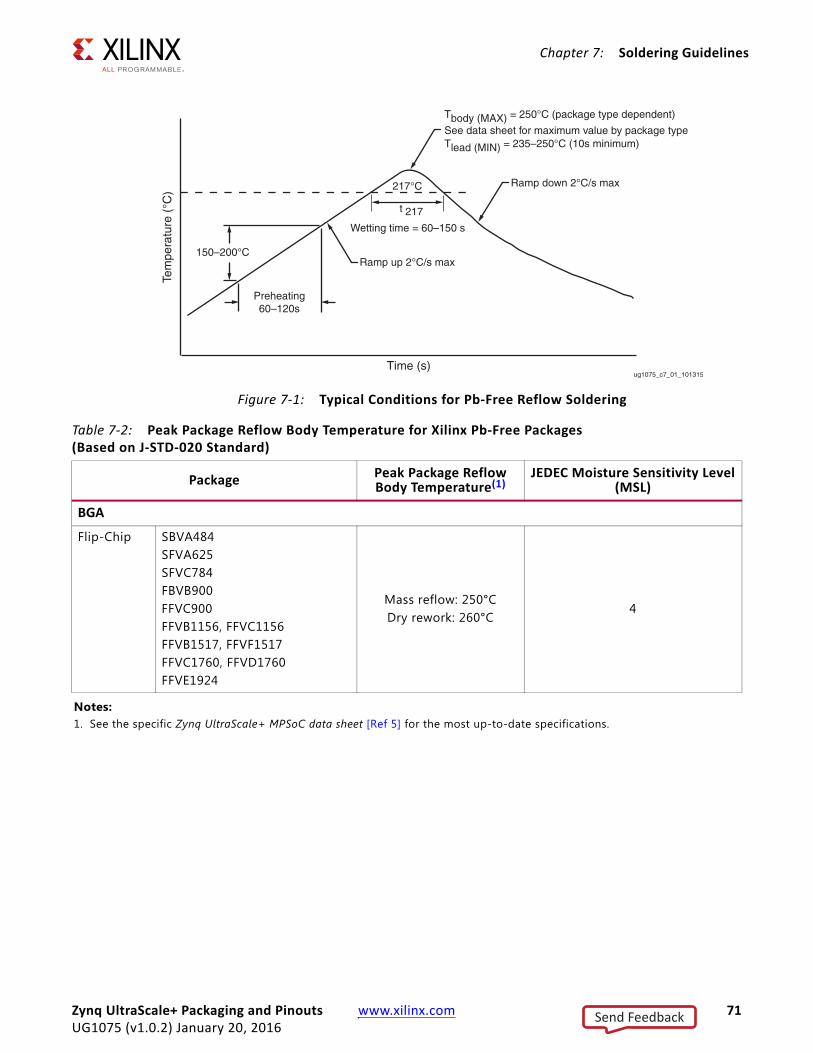
Chapter 7: Soldering Guidelines
X-Ref Target - Figure 7-1
Figure 7-1: Typical Conditions for Pb-Free Reflow Soldering
Wetting time = 60–150 s
217t
217°C
Ramp up 2°C/s max150–200°C
Time (s)
Preheating60–120s
Ramp down 2°C/s max
Tem
pera
ture
(°C
)
ug1075_c7_01_101315
Tbody (MAX) = 250°C (package type dependent)
Tlead (MIN) = 235–250°C (10s minimum)See data sheet for maximum value by package type
Table 7-2: Peak Package Reflow Body Temperature for Xilinx Pb-Free Packages (Based on J-STD-020 Standard)
Package Peak Package Reflow Body Temperature(1)
JEDEC Moisture Sensitivity Level (MSL)
BGA
Flip-Chip SBVA484SFVA625SFVC784FBVB900FFVC900FFVB1156, FFVC1156FFVB1517, FFVF1517FFVC1760, FFVD1760FFVE1924
Mass reflow: 250°CDry rework: 260°C
4
Notes: 1. See the specific Zynq UltraScale+ MPSoC data sheet [Ref 5] for the most up-to-date specifications.
Zynq UltraScale+ Packaging and Pinouts www.xilinx.com 71UG1075 (v1.0.2) January 20, 2016
Send Feedback

Chapter 7: Soldering Guidelines
For sophisticated boards with a substantial mix of large and small components, it is critical to minimize the ΔT across the board (<10°C) to minimize board warpage and thus, attain higher assembly yields. Minimizing the ΔT is accomplished by using a slower rate in the warm-up and preheating stages. Xilinx recommends a heating rate of less than 1°C/s during the preheating and soaking stages, in combination with a heating rate of not more than 3°C/s throughout the rest of the profile.
It is also important to minimize the temperature gradient on the component, between top surface and bottom side, especially during the cooling down phase. The key is to optimize cooling while maintaining a minimal temperature differential between the top surface of the package and the solder joint area. The temperature differential between the top surface of the component and the solder balls should be maintained at less than 7°C during the critical region of the cooling phase of the reflow process. This critical region is in the part of the cooling phase where the balls are not completely solidified to the board yet, usually between the 200°C–217°C range. To efficiently cool the parts, divide the cooling section into multiple zones, with each zone operating at different temperatures.
Post Reflow/Cleaning/Washing
Many PCB assembly subcontractors use a no-clean process in which no post-assembly washing is required. Although a no-clean process is recommended, if cleaning is required, Xilinx recommends a water-soluble paste and a washer using a deionized-water. Baking after the water wash is recommended to prevent fluid accumulation.
Cleaning solutions or solvents are not recommended because some solutions contain chemicals that can compromise the lid adhesive, thermal compound, or components inside the package.
Conformal Coating
Xilinx has no information about the reliability of flip-chip BGA packages on a board after exposure to conformal coating. Any process using conformal coating should be qualified for the specific use case to cover the materials and process steps.
RECOMMENDED: Xilinx does not recommend using Toluene-based conformal coatings because they can weaken the lid adhesive used in Xilinx packages.
Zynq UltraScale+ Packaging and Pinouts www.xilinx.com 72UG1075 (v1.0.2) January 20, 2016
Send Feedback
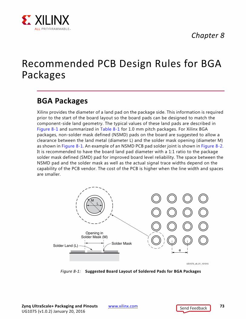
Chapter 8
Recommended PCB Design Rules for BGA Packages
BGA PackagesXilinx provides the diameter of a land pad on the package side. This information is required prior to the start of the board layout so the board pads can be designed to match the component-side land geometry. The typical values of these land pads are described in Figure 8-1 and summarized in Table 8-1 for 1.0 mm pitch packages. For Xilinx BGA packages, non-solder mask defined (NSMD) pads on the board are suggested to allow a clearance between the land metal (diameter L) and the solder mask opening (diameter M) as shown in Figure 8-1. An example of an NSMD PCB pad solder joint is shown in Figure 8-2. It is recommended to have the board land pad diameter with a 1:1 ratio to the package solder mask defined (SMD) pad for improved board level reliability. The space between the NSMD pad and the solder mask as well as the actual signal trace widths depend on the capability of the PCB vendor. The cost of the PCB is higher when the line width and spaces are smaller.
X-Ref Target - Figure 8-1
Figure 8-1: Suggested Board Layout of Soldered Pads for BGA Packages
Solder Mask
e
Opening inSolder Mask (M)
ML
Solder Land (L)
UG1075_c8_01_101315
Zynq UltraScale+ Packaging and Pinouts www.xilinx.com 73UG1075 (v1.0.2) January 20, 2016
Send Feedback
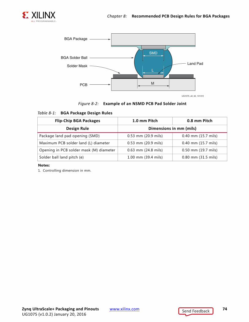
Chapter 8: Recommended PCB Design Rules for BGA Packages
X-Ref Target - Figure 8-2
Figure 8-2: Example of an NSMD PCB Pad Solder Joint
Table 8-1: BGA Package Design Rules
Flip-Chip BGA Packages 1.0 mm Pitch 0.8 mm Pitch
Design Rule Dimensions in mm (mils)
Package land pad opening (SMD) 0.53 mm (20.9 mils) 0.40 mm (15.7 mils)
Maximum PCB solder land (L) diameter 0.53 mm (20.9 mils) 0.40 mm (15.7 mils)
Opening in PCB solder mask (M) diameter 0.63 mm (24.8 mils) 0.50 mm (19.7 mils)
Solder ball land pitch (e) 1.00 mm (39.4 mils) 0.80 mm (31.5 mils)
Notes: 1. Controlling dimension in mm.
Land Pad
SMD
M
BGA Package
BGA Solder Ball
Solder Mask
PCB
UG1075_c8_02_101315
L
Zynq UltraScale+ Packaging and Pinouts www.xilinx.com 74UG1075 (v1.0.2) January 20, 2016
Send Feedback
Chapter 9
Thermal Specifications
IntroductionZynq UltraScale+ MPSoCs are offered exclusively in thermally efficient flip-chip BGA packages. These flip-chip packages range in pin-count from the smaller 19 x 19 mm SBVA484 to the 45 x 45 mm FFVE1924. This suite of packages is used to address the various power requirements of the Zynq UltraScale+ MPSoCs. Zynq UltraScale+ MPSoCs are implemented in the 16 nm process technology.
Unlike features in an ASIC, the combination of MPSoC features used in a user application is not known to the component supplier. Therefore, it remains a challenge for Xilinx to predict the power requirements of a given MPSoC when it leaves the factory. Accurate estimates are obtained when the board design takes shape. For this purpose, Xilinx offers and supports a suite of integrated device power analysis tools to help users quickly and accurately estimate their design power requirements. Zynq UltraScale+ MPSoCs are supported similarly to previous products. The uncertainty of design power requirements makes it difficult to apply canned thermal solutions to fit all users. Therefore, Xilinx devices do not come with preset thermal solutions. Your design’s operating conditions dictate the appropriate solution.
Thermal Resistance DataTable 9-1 shows the thermal resistance data for Zynq UltraScale+ MPSoCs (grouped in the packages offered). The data includes junction-to-ambient in still air, junction-to-case, and junction-to-board data based on standard JEDEC four-layer measurements.
IMPORTANT: The data in Table 9-1 is for device/package comparison purposes only. Attempts to recreate this data are only valid using the transient 2-phase measurement techniques outlined in JESD51-14.
TIP: The thermal data query for all available devices by package is available on the Xilinx website: www.xilinx.com/cgi-bin/thermal/thermal.pl.
Zynq UltraScale+ Packaging and Pinouts www.xilinx.com 75UG1075 (v1.0.2) January 20, 2016
Send Feedback
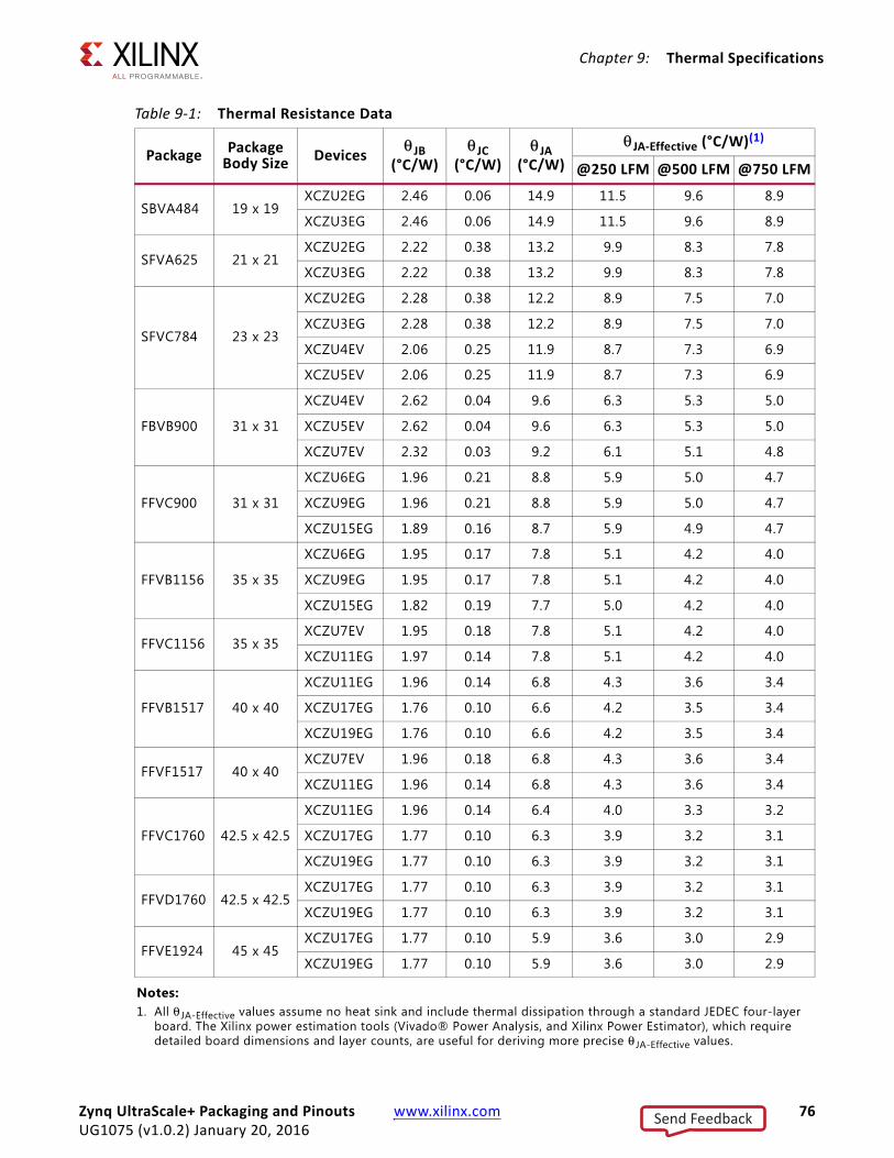
Chapter 9: Thermal Specifications
Table 9-1: Thermal Resistance Data
Package PackageBody Size Devices θ JB
(°C/W)θ JC
(°C/W)θ JA
(°C/W)θ JA-Effective (°C/W)(1)
@250 LFM @500 LFM @750 LFM
SBVA484 19 x 19XCZU2EG 2.46 0.06 14.9 11.5 9.6 8.9
XCZU3EG 2.46 0.06 14.9 11.5 9.6 8.9
SFVA625 21 x 21XCZU2EG 2.22 0.38 13.2 9.9 8.3 7.8
XCZU3EG 2.22 0.38 13.2 9.9 8.3 7.8
SFVC784 23 x 23
XCZU2EG 2.28 0.38 12.2 8.9 7.5 7.0
XCZU3EG 2.28 0.38 12.2 8.9 7.5 7.0
XCZU4EV 2.06 0.25 11.9 8.7 7.3 6.9
XCZU5EV 2.06 0.25 11.9 8.7 7.3 6.9
FBVB900 31 x 31
XCZU4EV 2.62 0.04 9.6 6.3 5.3 5.0
XCZU5EV 2.62 0.04 9.6 6.3 5.3 5.0
XCZU7EV 2.32 0.03 9.2 6.1 5.1 4.8
FFVC900 31 x 31
XCZU6EG 1.96 0.21 8.8 5.9 5.0 4.7
XCZU9EG 1.96 0.21 8.8 5.9 5.0 4.7
XCZU15EG 1.89 0.16 8.7 5.9 4.9 4.7
FFVB1156 35 x 35
XCZU6EG 1.95 0.17 7.8 5.1 4.2 4.0
XCZU9EG 1.95 0.17 7.8 5.1 4.2 4.0
XCZU15EG 1.82 0.19 7.7 5.0 4.2 4.0
FFVC1156 35 x 35XCZU7EV 1.95 0.18 7.8 5.1 4.2 4.0
XCZU11EG 1.97 0.14 7.8 5.1 4.2 4.0
FFVB1517 40 x 40
XCZU11EG 1.96 0.14 6.8 4.3 3.6 3.4
XCZU17EG 1.76 0.10 6.6 4.2 3.5 3.4
XCZU19EG 1.76 0.10 6.6 4.2 3.5 3.4
FFVF1517 40 x 40XCZU7EV 1.96 0.18 6.8 4.3 3.6 3.4
XCZU11EG 1.96 0.14 6.8 4.3 3.6 3.4
FFVC1760 42.5 x 42.5
XCZU11EG 1.96 0.14 6.4 4.0 3.3 3.2
XCZU17EG 1.77 0.10 6.3 3.9 3.2 3.1
XCZU19EG 1.77 0.10 6.3 3.9 3.2 3.1
FFVD1760 42.5 x 42.5XCZU17EG 1.77 0.10 6.3 3.9 3.2 3.1
XCZU19EG 1.77 0.10 6.3 3.9 3.2 3.1
FFVE1924 45 x 45XCZU17EG 1.77 0.10 5.9 3.6 3.0 2.9
XCZU19EG 1.77 0.10 5.9 3.6 3.0 2.9
Notes: 1. All θ JA-Effective values assume no heat sink and include thermal dissipation through a standard JEDEC four-layer
board. The Xilinx power estimation tools (Vivado® Power Analysis, and Xilinx Power Estimator), which require detailed board dimensions and layer counts, are useful for deriving more precise θ JA-Effective values.
Zynq UltraScale+ Packaging and Pinouts www.xilinx.com 76UG1075 (v1.0.2) January 20, 2016
Send Feedback
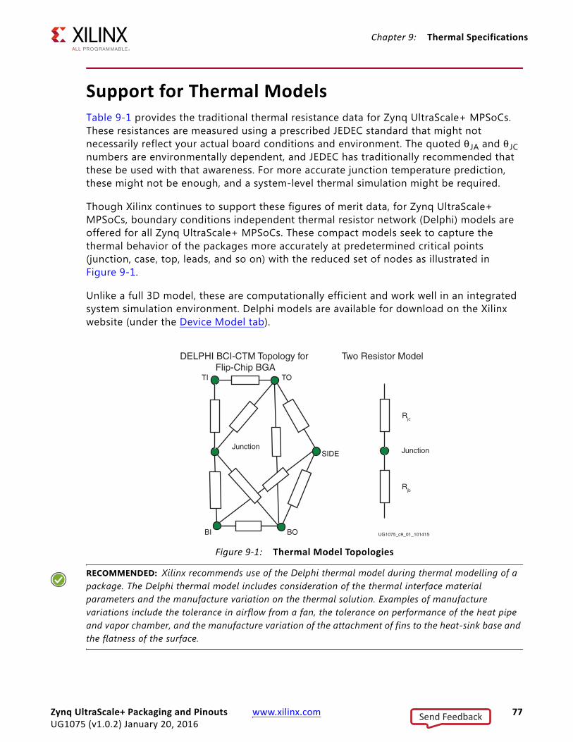
Chapter 9: Thermal Specifications
Support for Thermal ModelsTable 9-1 provides the traditional thermal resistance data for Zynq UltraScale+ MPSoCs. These resistances are measured using a prescribed JEDEC standard that might not necessarily reflect your actual board conditions and environment. The quoted θ JA and θ JC numbers are environmentally dependent, and JEDEC has traditionally recommended that these be used with that awareness. For more accurate junction temperature prediction, these might not be enough, and a system-level thermal simulation might be required.
Though Xilinx continues to support these figures of merit data, for Zynq UltraScale+ MPSoCs, boundary conditions independent thermal resistor network (Delphi) models are offered for all Zynq UltraScale+ MPSoCs. These compact models seek to capture the thermal behavior of the packages more accurately at predetermined critical points (junction, case, top, leads, and so on) with the reduced set of nodes as illustrated in Figure 9-1.
Unlike a full 3D model, these are computationally efficient and work well in an integrated system simulation environment. Delphi models are available for download on the Xilinx website (under the Device Model tab).
RECOMMENDED: Xilinx recommends use of the Delphi thermal model during thermal modelling of a package. The Delphi thermal model includes consideration of the thermal interface material parameters and the manufacture variation on the thermal solution. Examples of manufacture variations include the tolerance in airflow from a fan, the tolerance on performance of the heat pipe and vapor chamber, and the manufacture variation of the attachment of fins to the heat-sink base and the flatness of the surface.
X-Ref Target - Figure 9-1
Figure 9-1: Thermal Model Topologies
TI
Junction
BI BO
TO
SIDE
UG1075_c9_01_101415
DELPHI BCI-CTM Topology for Flip-Chip BGA
Junction
Rjc
Rjb
Two Resistor Model
Zynq UltraScale+ Packaging and Pinouts www.xilinx.com 77UG1075 (v1.0.2) January 20, 2016
Send Feedback

Chapter 10
Thermal Management Strategy
IntroductionAs described in this section, Xilinx relies on a multi-pronged approach to consuming less power and dissipating heat for systems using Zynq UltraScale+ MPSoCs.
Flip-Chip PackagesZynq UltraScale+ MPSoCs are offered in flip-chip BGA packages, which present a low thermal path. With the exception of the bare-die packages, the flip-chip BGA packages incorporate a heat spreader with an additional thermal interface material (TIM), as shown in Figure 10-1.
Materials with better thermal conductivity and consistent process deliver low thermal resistance to the heat spreader.
A parallel effort to ensure optimized package electrical return paths produces the added benefit of enhanced power and ground plane arrangement in the packages. A boost in copper density on the planes improves the overall thermal conductivity through the laminate. In addition, the extra dense and distributed via fields in the package increase the vertical thermal conductivity.
X-Ref Target - Figure 10-1
Figure 10-1: Heat Spreader with Thermal Interface Material
Die
Lid-Heat Spreader
Substrate
Thermal Interface Material (TIM)
UG1075_c10_01_101415
Zynq UltraScale+ Packaging and Pinouts www.xilinx.com 78UG1075 (v1.0.2) January 20, 2016
Send Feedback
Chapter 10: Thermal Management Strategy
System Level Heat Sink SolutionsTo complete a comprehensive thermal management strategy, an overall thermal budget that includes custom or OEM heat sink solutions depends on the physical and mechanical constraints of the system. A heat-sink solution, managed by the system-level designer, should be tailored to the design and specific system constraints. This includes understanding the inherent device capabilities for delivering heat to the surface.
Thermal Interface MaterialWhen installing heat sinks for Zynq UltraScale+ MPSoCs, a suitable thermal interface material (TIM) must be used. This thermal material significantly aids the transfer of heat from the component to the heat sink.
For lidless flip-chip BGAs, the surface of the silicon contacts the heat sink. For lidded flip-chip BGAs, the lid contacts the heat sink. The surface size of the lidless flip-chip BGA and lidded flip-chip BGAs are different. Xilinx recommends a different type of thermal material for long-term use with each type of flip-chip BGAs package.
Thermal interface material is needed because even the largest heat sink and fan cannot effectively cool an Zynq UltraScale+ MPSoC unless there is good physical contact between the base of the heat sink and the top of the Zynq UltraScale+ MPSoC. The surfaces of both the heat sink and the Zynq UltraScale+ MPSoC silicon are not absolutely smooth. This surface roughness is observed when examined at a microscopic level. Because surface roughness reduces the effective contact area, attaching a heat sink without a thermal interface material is not sufficient due to inadequate surface contact.
A thermal interface material such as phase-change material, thermal grease, or thermal pads fills these gaps and allows effective transference of heat between the Zynq UltraScale+ MPSoC die and the heat sink.
The selection of the thermal interface (TIM) between the package and the thermal management solution is critical to ensure the lowest thermal contact resistance. Therefore, the following parameters must be considered.
1. The flatness of the lid and the flatness of the contact surface of the thermal solution.
2. The applied pressure of the thermal solution on the package, which must be within the allowable maximum pressure that can be applied on the package.
3. The total thermal contact of the thermal interface material. This value is determined based on the parameters in step 1 and step 2, which are published in the data sheet of the thermal interface supplier.
Zynq UltraScale+ Packaging and Pinouts www.xilinx.com 79UG1075 (v1.0.2) January 20, 2016
Send Feedback
Chapter 10: Thermal Management Strategy
Types of TIMThere are many type of TIM available for sale. The most commonly used thermal interface materials are listed.
• Thermal grease
• Thermal pads
• Phase change material
• Thermal paste
• Thermal adhesives
• Thermal tape
Guidelines for Thermal Interface MaterialsFive factors affect the choice, use, and performance of the interface material used between the processor and the heat sink:
• Thermal Conductivity of the Material
• Electrical Conductivity of the Material
• Spreading Characteristics of the Material
• Long-Term Stability and Reliability of the Material
• Ease of Application
• Applied Pressure from Heat Sink to the Package via Thermal Interface Materials
Thermal Conductivity of the Material
Thermal conductivity is the quantified ability of any material to transfer heat. The thermal conductivity of the interface material has a significant impact on its thermal performance. The higher the thermal conductivity, the more efficient the material is at transferring heat. Materials that have a lower thermal conductivity are less efficient at transferring heat, causing a higher temperature differential to exist across the interface. To overcome this less efficient heat transfer, a better cooling solution (typically, a more costly solution) must be used to achieve the desired heat dissipation.
Electrical Conductivity of the Material
Some metal-based TIM compounds are electrically conductive. Ceramic-based compounds are typically not electrically conductive. Manufacturers produce metal-based compounds with low-electrical conductivity, but some of these materials are not completely electrically inert. Metal-based thermal compounds are not hazardous to the Zynq UltraScale+ MPSoC die itself, but other elements on the Zynq UltraScale+ MPSoC or motherboard can be at risk
Zynq UltraScale+ Packaging and Pinouts www.xilinx.com 80UG1075 (v1.0.2) January 20, 2016
Send Feedback
Chapter 10: Thermal Management Strategy
if they become contaminated by the compound. For this reason, Xilinx does not recommend the use of electrically conductive thermal interface material.
Spreading Characteristics of the Material
The spreading characteristics of the thermal interface material determines its ability, under the pressure of the mounted heat sink, to spread and fill in or eliminate the air gaps between the Zynq UltraScale+ MPSoC and the heat sink. Because air is a very poor thermal conductor, the more completely the interface material fills the gaps, the greater the heat transference.
Long-Term Stability and Reliability of the Material
The long-term stability and reliability of the thermal interface material is described as the ability to provide a sufficient thermal conductance even after an extended time or extensive. Low-quality compounds can harden or leak out over time (the pump-out effect), leading to overheating or premature failure of the Zynq UltraScale+ MPSoC. High-quality compounds provide a stable and reliable thermal interface material throughout the lifetime of the device. Thermal greases with higher viscosities are typically more resistant to pump out effects on lidless devices.
Ease of Application
A spreadable thermal grease requires the surface mount supplier to carefully use the appropriate amount of material. Too much or too little material can cause problems. The thermal pad is a fixed size and is therefore easier to apply in a consistent manner.
Applied Pressure from Heat Sink to the Package via Thermal Interface Materials
RECOMMENDED: Xilinx recommends that the applied pressure on the package be in the range of 20 to 40 PSI for optimum performance of the thermal interface material (TIM) between the package and the heat sink. Thermocouples should not be present between the package and the heat sink, as their presence will degrade the thermal contact and result in incorrect thermal measurements.
Zynq UltraScale+ Packaging and Pinouts www.xilinx.com 81UG1075 (v1.0.2) January 20, 2016
Send Feedback

Chapter 10: Thermal Management Strategy
RECOMMENDED: Xilinx recommends using dynamic mounting around the four corners of the device package. On the PCB, use a bracket clip as part of the heat sink attachment to provide mechanical package support. See Figure 10-2.
Heat Sink Removal ProcedureThe heat spreader on the package provides mechanical protection for the die and serves as the primary heat dissipation path. It is attached with an epoxy adhesive to provide the necessary adhesion strength to hold the package together. For an application in which an external heat sink subjects the lid adhesion joint to continuous tension or shear, extra support might be required.
In addition, if the removal of an attached external heat sink subjects the joint to tension, torque, or shear, care should be exercised to ensure that the lid itself does not come off. In such cases, it has been found useful to use a small metal blade or metal wire to break the lid to heat sink joint from the corners and carefully pry the heat sink off. The initial cut should reach far in enough so that the blade has leverage to exert upward pressure against the heat sink. Contact the heat sink and heat sink adhesive manufacturer for more specific recommendations on heat sink removal.
X-Ref Target - Figure 10-2
Figure 10-2: Dynamic Mounting and Bracket Clips on Heat Sink Attachment
PKG
Heat SinkHS Base
Zynq UltraScale+ Packaging and Pinouts www.xilinx.com 82UG1075 (v1.0.2) January 20, 2016
Send Feedback
Chapter 11
Heat Sink Guidelines for Lidless Flip-Chip Packages
Heat Sink Attachments for Lidless FB PackagesHeat sinks can be attached to the package in multiple ways. For heat to dissipate effectively, the advantages and disadvantages of each heat sink attachment method must be considered. Factors influencing the selection of the heat sink attachment method include the package type, contact area of the heat source, and the heat sink type.
Silicon and Decoupling Capacitors Height ConsiderationWhen designing heat sink attachments for lidless flip-chip BGA packages, the height of the die above the substrate and also the height of decoupling capacitors must be considered (Figure 11-1). This is to prevent electrical shorting between the heat sink (metal) and the decoupling capacitors.
X-Ref Target - Figure 11-1
Figure 11-1: Cross Section of Lidless Flip-chip BGA
Silicon Underfill SubstrateDecouplingCapacitor
UG1075_c11_01_101415
Zynq UltraScale+ Packaging and Pinouts www.xilinx.com 83UG1075 (v1.0.2) January 20, 2016
Send Feedback

Chapter 11: Heat Sink Guidelines for Lidless Flip-Chip Packages
Types of Heat Sink AttachmentsThere are six main methods for heat sink attachment. Table 11-1 lists their advantages and disadvantages.
• Thermal tape
• Thermally conductive adhesive or glue
• Wire form Z-clips
• Plastic clip-ons
• Threaded stand-offs (PEMs) and compression springs
• Push-pins and compression springs
Table 11-1: Heat Sink Attachment Methods
Attachment Method Advantages Disadvantages
Thermal tape • Generally easy to attach and is inexpensive.• Lowest cost approach for aluminum heat
sink attachment.• No additional space required on the PCB.
• The surfaces of the heat sink and the chip must be very clean to allow the tape to bond correctly.
• Because of the small contact area, the tape might not provide sufficient bond strength.
• Tape is a moderate to low thermal conductor that could affect the thermal performance.
Thermally conductive adhesive or glue
• Outstanding mechanical adhesion.• Fairly inexpensive, costs a little more than
tape.• No additional space required on the PCB.
• Adhesive application process is challenging and it is difficult to control the amount of adhesive to use.
• Difficult to rework.• Because of the small contact area, the
adhesive might not provide sufficient bond strength.
Wire form Z-clips • It provides a strong and secure mechanical attachment. In environments that require shock and vibration testing, this type of strong mechanical attachment is necessary.
• Easy to apply and remove. Does not cause the semiconductors to be destroyed (epoxy and occasionally tape can destroy the device).
• It applies a preload onto the thermal interface material (TIM). Pre-loads actually improve thermal performance.
• Requires additional space on the PCB for anchor locations.
Zynq UltraScale+ Packaging and Pinouts www.xilinx.com 84UG1075 (v1.0.2) January 20, 2016
Send Feedback

Chapter 11: Heat Sink Guidelines for Lidless Flip-Chip Packages
Heat Sink Attachment
Component Pick-up Tool Consideration
For pick-and-place machines to place lidless flip-chip BGAs onto PCBs, Xilinx recommends using soft tips or suction cups for the nozzles. This prevents chipping, scratching, or even cracking of the bare die (Figure 11-2).
Plastic clip-ons • Suitable for designs where space on the PCB is limited.
• Easy to rework by allowing heat sinks to be easily removed and reapplied without damaging the PCB board.
• Can provide a strong enough mechanical attachment to pass shock and vibration test.
• Needs a keep out area around the silicon devices to use the clip.
• Caution is required when installing or removing clip-ons because localized stress can damage the solder balls or chip substrate.
Threaded stand-offs (PEMs) and compression springs
• Provides stable attachments to heat source and transfers load to the PCB, backing plate, or chassis.
• Suitable for high mass heat sinks.• Allows for tight control over mounting
force and load placed on chip and solder balls.
• Holes are required in the PCB taking valuable space that can be used for trace lines.
• Tends to be expensive, especially since holes need to be drilled or predrilled onto the PCB board to use stand-offs.
Push-pins and compression springs
• Provides a stable attachment to a heat source and transfers load to the PCB.
• Allows for tight control over mounting force and load placed on chip and solder balls.
• Requires additional space on the PCB for push-pin locations.
Table 11-1: Heat Sink Attachment Methods (Cont’d)
Attachment Method Advantages Disadvantages
X-Ref Target - Figure 11-2
Figure 11-2: Recommended Method For Using Pick-up Tools
UG1075_c11_02_101415
Silicon Substrate
MetalTip
Nozzle
Metal Pick Up Tip Nozzle with Soft Tips orSuction Cups is Preferred
Soft Tips
DecouplingCapacitor
Preferred
Silicon Substrate
MetalTip
Nozzle
Metal Pick Up Tip Nozzle Can Damagethe Exposed Silicon
DecouplingCapacitor
Incorrect Pickup Method
Zynq UltraScale+ Packaging and Pinouts www.xilinx.com 85UG1075 (v1.0.2) January 20, 2016
Send Feedback
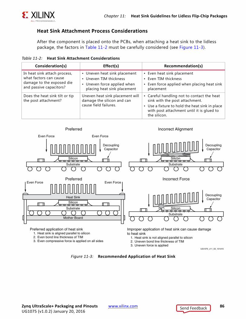
Chapter 11: Heat Sink Guidelines for Lidless Flip-Chip Packages
Heat Sink Attachment Process Considerations
After the component is placed onto the PCBs, when attaching a heat sink to the lidless package, the factors in Table 11-2 must be carefully considered (see Figure 11-3).
Table 11-2: Heat Sink Attachment Considerations
Consideration(s) Effect(s) Recommendation(s)
In heat sink attach process, what factors can cause damage to the exposed die and passive capacitors?
• Uneven heat sink placement• Uneven TIM thickness• Uneven force applied when
placing heat sink placement
• Even heat sink placement• Even TIM thickness• Even force applied when placing heat sink
placement
Does the heat sink tilt or tip the post attachment?
Uneven heat sink placement will damage the silicon and can cause field failures.
• Careful handling not to contact the heat sink with the post attachment.
• Use a fixture to hold the heat sink in place with post attachment until it is glued to the silicon.
X-Ref Target - Figure 11-3
Figure 11-3: Recommended Application of Heat Sink
UG1075_c11_03_101415
Silicon
Substrate
DecouplingCapacitor
Even ForceEven Force
Silicon
Heat Sink
Mother Board
Substrate
Even ForceEven Force
Preferred
Preferred
Incorrect Alignment
Silicon
Substrate
DecouplingCapacitor
Incorrect Force
Silicon
Substrate
DecouplingCapacitor
Preferred application of heat sink 1. Heat sink is aligned parallel to silicon 2. Even bond line thickness of TIM 3. Even compressive force is applied on all sides
Improper application of heat sink can cause damage to heat sink 1. Heat sink is not aligned parallel to silicon 2. Uneven bond line thickness of TIM 3. Uneven force is applied
Zynq UltraScale+ Packaging and Pinouts www.xilinx.com 86UG1075 (v1.0.2) January 20, 2016
Send Feedback
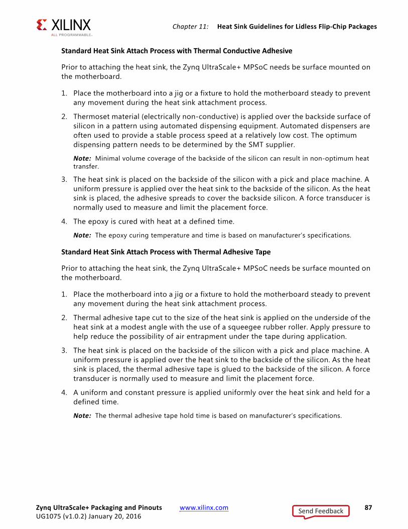
Chapter 11: Heat Sink Guidelines for Lidless Flip-Chip Packages
Standard Heat Sink Attach Process with Thermal Conductive Adhesive
Prior to attaching the heat sink, the Zynq UltraScale+ MPSoC needs be surface mounted on the motherboard.
1. Place the motherboard into a jig or a fixture to hold the motherboard steady to prevent any movement during the heat sink attachment process.
2. Thermoset material (electrically non-conductive) is applied over the backside surface of silicon in a pattern using automated dispensing equipment. Automated dispensers are often used to provide a stable process speed at a relatively low cost. The optimum dispensing pattern needs to be determined by the SMT supplier.
Note: Minimal volume coverage of the backside of the silicon can result in non-optimum heat transfer.
3. The heat sink is placed on the backside of the silicon with a pick and place machine. A uniform pressure is applied over the heat sink to the backside of the silicon. As the heat sink is placed, the adhesive spreads to cover the backside silicon. A force transducer is normally used to measure and limit the placement force.
4. The epoxy is cured with heat at a defined time.
Note: The epoxy curing temperature and time is based on manufacturer’s specifications.
Standard Heat Sink Attach Process with Thermal Adhesive Tape
Prior to attaching the heat sink, the Zynq UltraScale+ MPSoC needs be surface mounted on the motherboard.
1. Place the motherboard into a jig or a fixture to hold the motherboard steady to prevent any movement during the heat sink attachment process.
2. Thermal adhesive tape cut to the size of the heat sink is applied on the underside of the heat sink at a modest angle with the use of a squeegee rubber roller. Apply pressure to help reduce the possibility of air entrapment under the tape during application.
3. The heat sink is placed on the backside of the silicon with a pick and place machine. A uniform pressure is applied over the heat sink to the backside of the silicon. As the heat sink is placed, the thermal adhesive tape is glued to the backside of the silicon. A force transducer is normally used to measure and limit the placement force.
4. A uniform and constant pressure is applied uniformly over the heat sink and held for a defined time.
Note: The thermal adhesive tape hold time is based on manufacturer’s specifications.
Zynq UltraScale+ Packaging and Pinouts www.xilinx.com 87UG1075 (v1.0.2) January 20, 2016
Send Feedback

Chapter 11: Heat Sink Guidelines for Lidless Flip-Chip Packages
Push-Pin and Shoulder Screw Heat Sink Attachment Process with Phase Change Material (PCM) Application
Prior to attaching the heat sink, the Zynq UltraScale+ MPSoC needs be surface mounted on the motherboard.
1. Place the motherboard into a jig or a fixture to hold the motherboard steady to prevent any movement during the heat sink attachment process.
Note: The jig or fixture needs to account for the push pin depth of the heat sink.
2. PCM tape, cut to the size of the heat sink, is applied on the underside of the heat sink at a modest angle with the use of a squeegee rubber roller. Apply pressure to help reduce the possibility of air entrapment under the tape during application.
3. Using the push-pin tool, heat sinks are applied over the packages ensuring a pin locking action with the PCB holes. The compression load from springs applies the appropriate mounting pressure required for proper thermal interface material performance.
Note: Heat sinks must not tilt during installation. This process cannot be automated due to the mechanical locking action which requires manual handling. The PCB drill hole tolerances need to be close enough to eliminate any issues concerning the heat sink attachment.
Zynq UltraScale+ Packaging and Pinouts www.xilinx.com 88UG1075 (v1.0.2) January 20, 2016
Send Feedback
Appendix A
Additional Resources and Legal Notices
Xilinx ResourcesFor support resources such as Answers, Documentation, Downloads, and Forums, see Xilinx Support.
Solution CentersSee the Xilinx Solution Centers for support on devices, software tools, and intellectual property at all stages of the design cycle. Topics include design assistance, advisories, and troubleshooting tips.
References1. Zynq UltraScale+ MPSoC Overview (DS891)
2. Zynq UltraScale+ MPSoC Packaging Specifications
3. UltraScale Architecture SelectIO Resources User Guide (UG571)
4. UltraScale Architecture Clocking Resources User Guide (UG572)
5. Zynq UltraScale+ MPSoC Data Sheet: DC and AC Switching Characteristics (DS925)
6. Zynq UltraScale+ MPSoC Technical Reference Manual (UG1085)
7. UltraScale Architecture GTH Transceiver User Guide (UG576)
8. UltraScale Architecture GTY Transceiver User Guide (UG578)
9. UltraScale Architecture System Monitor User Guide (UG580)
10. UltraScale Architecture PCB and Pin Planning User Guide (UG583)
11. UltraScale Architecture-Based Memory Interface Solutions Product Guide (PG150)
Zynq UltraScale+ Packaging and Pinouts www.xilinx.com 89UG1075 (v1.0.2) January 20, 2016
Send Feedback
Appendix A: Additional Resources and Legal Notices
12. The following websites contain additional information on heat management and contact information.
° Wakefield: www.wakefield-vette.com
° Aavid: www.aavid.com
° Advanced Thermal Solutions: www.qats.com
° Radian Thermal Products: www.radianheatsinks.com
° Thermo Cool: www.thermocoolcorp.com
° CTS: www.ctscorp.com
13. Refer to the following websites for interface material sources:
° Henkel: www.henkel.com
° Bergquist Company: www.bergquistcompany.com
° AOS Thermal Compound: www.aosco.com
° Chomerics: www.chomerics.com
° Kester: www.kester.com
14. Refer to the following websites for CFD tools Xilinx supports with thermal models.
° Mentor Flotherm: www.mentor.com/products/mechanical/flotherm/flotherm/
° ANSYS Icepak: www.ansys.com
15. Refer to the thermal device models on xilinx.com.
16. The following papers are referenced for more information on thermal modelling.
° Lemczyk, T.F., Mack, B., Culham, J.R. and Yovanovich, M.M., 1992, “Printed Circuit Board Trace Thermal Analysis and Effective Conductivity”, ASME J. Electronic Packaging, Vol. 114, pp. 413 - 419.50.
° Refai-Ahmed, G. and Karimanal, K., 2003, “Validation of Compact Conduction Models of BGA Under Realistic Boundary,” J. of Components and Packaging Technology, Vol. 26, No. 3, pp. 610-615.
° Sansoucy, E, Refai-Ahmed, G., and Karimanal, K., 2002, “Thermal Characterization of TBGA Package for an integration in Board Level Analysis,” Eighth Intersociety on Thermal Conference Phenomena in Electronic Systems, San Diego., USA.
° Karimanal,K and Refai-Ahmed, G., and., 2002, “Validation of Compact Conduction Models of BGA Under Realistic Boundary Conditions,” Eighth Intersociety on Thermal Conference Phenomena in Electronic Systems, San Diego, USA.
° "Karminal, K. and Refai-Ahmed, G., 2001, ``Compact conduction Model (CCM) of Microelectronic Packages- A BGA Validation Study,'' APACK Conference on Advance in Packaging, Singapore.
Zynq UltraScale+ Packaging and Pinouts www.xilinx.com 90UG1075 (v1.0.2) January 20, 2016
Send Feedback
Appendix A: Additional Resources and Legal Notices
Please Read: Important Legal NoticesThe information disclosed to you hereunder (the “Materials”) is provided solely for the selection and use of Xilinx products. To the maximum extent permitted by applicable law: (1) Materials are made available "AS IS" and with all faults, Xilinx hereby DISCLAIMS ALL WARRANTIES AND CONDITIONS, EXPRESS, IMPLIED, OR STATUTORY, INCLUDING BUT NOT LIMITED TO WARRANTIES OF MERCHANTABILITY, NON-INFRINGEMENT, OR FITNESS FOR ANY PARTICULAR PURPOSE; and (2) Xilinx shall not be liable (whether in contract or tort, including negligence, or under any other theory of liability) for any loss or damage of any kind or nature related to, arising under, or in connection with, the Materials (including your use of the Materials), including for any direct, indirect, special, incidental, or consequential loss or damage (including loss of data, profits, goodwill, or any type of loss or damage suffered as a result of any action brought by a third party) even if such damage or loss was reasonably foreseeable or Xilinx had been advised of the possibility of the same. Xilinx assumes no obligation to correct any errors contained in the Materials or to notify you of updates to the Materials or to product specifications. You may not reproduce, modify, distribute, or publicly display the Materials without prior written consent. Certain products are subject to the terms and conditions of Xilinx’s limited warranty, please refer to Xilinx’s Terms of Sale which can be viewed at www.xilinx.com/legal.htm#tos; IP cores may be subject to warranty and support terms contained in a license issued to you by Xilinx. Xilinx products are not designed or intended to be fail-safe or for use in any application requiring fail-safe performance; you assume sole risk and liability for use of Xilinx products in such critical applications, please refer to Xilinx’s Terms of Sale which can be viewed at www.xilinx.com/legal.htm#tos.Automotive Applications DisclaimerXILINX PRODUCTS ARE NOT DESIGNED OR INTENDED TO BE FAIL-SAFE, OR FOR USE IN ANY APPLICATION REQUIRING FAIL-SAFE PERFORMANCE, SUCH AS APPLICATIONS RELATED TO: (I) THE DEPLOYMENT OF AIRBAGS, (II) CONTROL OF A VEHICLE, UNLESS THERE IS A FAIL-SAFE OR REDUNDANCY FEATURE (WHICH DOES NOT INCLUDE USE OF SOFTWARE IN THE XILINX DEVICE TO IMPLEMENT THE REDUNDANCY) AND A WARNING SIGNAL UPON FAILURE TO THE OPERATOR, OR (III) USES THAT COULD LEAD TO DEATH OR PERSONAL INJURY. CUSTOMER ASSUMES THE SOLE RISK AND LIABILITY OF ANY USE OF XILINX PRODUCTS IN SUCH APPLICATIONS.© Copyright 2015–2016 Xilinx, Inc. Xilinx, the Xilinx logo, Artix, ISE, Kintex, Spartan, Virtex, Vivado, Zynq, and other designated brands included herein are trademarks of Xilinx in the United States and other countries. AMBA, AMBA Designer, ARM, ARM1176JZ-S, CoreSight, Cortex, and PrimeCell are trademarks of ARM in the EU and other countries. PCI, PCI Express, PCIe, and PCI-X are trademarks of PCI-SIG. All other trademarks are the property of their respective owners.
Zynq UltraScale+ Packaging and Pinouts www.xilinx.com 91UG1075 (v1.0.2) January 20, 2016
Send Feedback
Related Documents