SERVICE MANUAL Model Name Using Similar Mechanism CFD-S01 Optical Pick-up Mechanism Type KSM-213CDP PERSONAL AUDIO SYSTEM SPECIFICATIONS ZS-H10CP/H20CP Photo: ZS-H10CP Ver. 1.0 2006.03 9-887-131-01 2006C05-1 © 2006.03 Sony Corporation Personal Audio Division Published by Sony Techno Create Corporation US Model Canadian Model ZS-H10CP E Model ZS-H20CP AUDIO POWER SPECIFICATIONS P (H10CP: US model only) OWER OUTPUT AND TOTAL HARMONIC DISTORTION: With 3.2-ohm loads, both channels driven from 150 - 10 000 Hz; rated 1.4 W per channel-minimum RMS power, with no more than 10 % total harmonic distortion in AC operation. Other specifications CD player section System Compact disc digital audio system Laser diode properties Emission duration: Continuous Laser output: Less than 44.6 µW (This output is the value measured at a distance of about 200 mm from the objective lens surface on the optical pick-up block with 7 mm aperture.) Number of channels 2 Frequency response 20 - 20 000 Hz 1 dB Wow and flutter Below measurable limit Radio section Frequency range FM: 87.5 - 108 MHz – H10CP/H20CP: Mexican model – – H20CP: E model – AM: 530 - 1 710 kHz AM: 531 - 1 611 kHz (9 kHz step) 530 - 1 610 kHz (10 kHz step) Antennas FM: Telescopic antenna AM: Built-in ferrite bar antenna General Speaker Full range: 10 cm (3 7 /8 inches) dia., 3.2 Ω, cone type (2) (H10CP) Full range: 10 cm (3 7 /8 inches) dia., 6 Ω, cone type (2) (H20CP) Dimensions 1 /2 7 /8 Mass Approx. 6.4 kg (14 lb) (incl. batteries) Approx. 558 × 292 × 275 mm (w/h/d) (22 × 11 × 10 inches) (incl. projecting parts) Supplied accessories AC power adaptor (1) Design and specifications are subject to change without notice. Battery life CD playback Sony R20P: approx. 3 h (H10CP), approx. 1 h (H20CP) Sony alkaline LR20: approx. 10 h (H10CP), approx. 6 h (H20CP) Radio reception Sony R20P: approx. 14 h (H10CP), approx. 4 h (H20CP) Sony alkaline LR20: approx. 28 h (H10CP), approx. 13 h (H20CP) Outputs Headphones jack (stereo minijack): For 16 - 68 Ω impedance headphones Power output 2.3 W + 2.3 W (at 3.2 Ω, 10 % harmonic distortion) (H10CP) 4.5 W + 4.5 W (at 6 Ω, 10 % harmonic distortion) (H20CP) Power requirements DC IN 9 V jack accepts: Supplied AC power adaptor for use with 120 V AC, 60 Hz (H10CP/H20CP: Mexican model) 9 V DC, 6 R20 (size D) batteries Supplied AC power adaptor for use with 230 V AC, 50 Hz (H20CP: E model) Inputs AUDIO IN jack (stereo minijack): minimum input level 245 mV

Welcome message from author
This document is posted to help you gain knowledge. Please leave a comment to let me know what you think about it! Share it to your friends and learn new things together.
Transcript
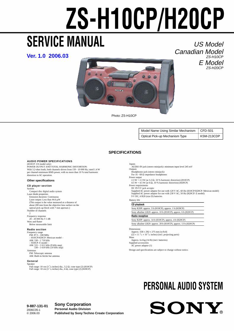
SERVICE MANUAL
Model Name Using Similar Mechanism CFD-S01
Optical Pick-up Mechanism Type KSM-213CDP
PERSONAL AUDIO SYSTEM
SPECIFICATIONS
ZS-H10CP/H20CP
Photo: ZS-H10CP
Ver. 1.0 2006.03
9-887-131-012006C05-1© 2006.03
Sony CorporationPersonal Audio DivisionPublished by Sony Techno Create Corporation
US ModelCanadian Model
ZS-H10CP
E ModelZS-H20CP
AUDIO POWER SPECIFICATIONS
P(H10CP: US model only)
OWER OUTPUT AND TOTAL HARMONIC DISTORTION:With 3.2-ohm loads, both channels driven from 150 - 10 000 Hz; rated 1.4 W per channel-minimum RMS power, with no more than 10 % total harmonic distortion in AC operation.
Other specifications
CD player sectionSystem
Compact disc digital audio systemLaser diode properties
Emission duration: ContinuousLaser output: Less than 44.6 µW(This output is the value measured at a distance of about 200 mm from the objective lens surface on the optical pick-up block with 7 mm aperture.)
Number of channels2
Frequency response20 - 20 000 Hz 1 dB
Wow and flutter Below measurable limit
Radio sectionFrequency range
FM: 87.5 - 108 MHz– H10CP/H20CP: Mexican model –
– H20CP: E model –AM: 530 - 1 710 kHz
AM: 531 - 1 611 kHz (9 kHz step) 530 - 1 610 kHz (10 kHz step)
AntennasFM: Telescopic antennaAM: Built-in ferrite bar antenna
GeneralSpeaker
Full range: 10 cm (3 7/8 inches) dia., 3.2 Ω, cone type (2) (H10CP)Full range: 10 cm (3 7/8 inches) dia., 6 Ω, cone type (2) (H20CP)
Dimensions
1/2 7/8Mass
Approx. 6.4 kg (14 lb) (incl. batteries)
Approx. 558 × 292 × 275 mm (w/h/d)(22 × 11 × 10 inches) (incl. projecting parts)
Supplied accessoriesAC power adaptor (1)
Design and specifications are subject to change without notice.
Battery life
CD playback Sony R20P: approx. 3 h (H10CP), approx. 1 h (H20CP)
Sony alkaline LR20: approx. 10 h (H10CP), approx. 6 h (H20CP)
Radio receptionSony R20P: approx. 14 h (H10CP), approx. 4 h (H20CP)
Sony alkaline LR20: approx. 28 h (H10CP), approx. 13 h (H20CP)
OutputsHeadphones jack (stereo minijack):For 16 - 68 Ω impedance headphones
Power output2.3 W + 2.3 W (at 3.2 Ω, 10 % harmonic distortion) (H10CP)4.5 W + 4.5 W (at 6 Ω, 10 % harmonic distortion) (H20CP)
Power requirementsDC IN 9 V jack accepts:Supplied AC power adaptor for use with 120 V AC, 60 Hz (H10CP/H20CP: Mexican model)
9 V DC, 6 R20 (size D) batteriesSupplied AC power adaptor for use with 230 V AC, 50 Hz (H20CP: E model)
InputsAUDIO IN jack (stereo minijack): minimum input level 245 mV
2
ZS-H10CP/H20CP
Notes on chip component replacement• Never reuse a disconnected chip component.• Notice that the minus side of a tantalum capacitor may be
damaged by heat.
Flexible Circuit Board Repairing• Keep the temperature of the soldering iron around 270 ˚C
during repairing.• Do not touch the soldering iron on the same conductor of the
circuit board (within 3 times).• Be careful not to apply force on the conductor when soldering
or unsoldering.
SAFETY-RELATED COMPONENT WARNING!!
COMPONENTS IDENTIFIED BY MARK 0 OR DOTTED LINEWITH MARK 0 ON THE SCHEMATIC DIAGRAMS AND INTHE PARTS LIST ARE CRITICAL TO SAFE OPERATION.REPLACE THESE COMPONENTS WITH SONY PARTS WHOSEPART NUMBERS APPEAR AS SHOWN IN THIS MANUAL ORIN SUPPLEMENTS PUBLISHED BY SONY.
CAUTIONUse of controls or adjustments or performance of proceduresother than those specified herein may result in hazardous radiationexposure.
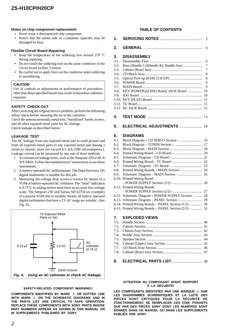
SAFETY CHECK-OUTAfter correcting the original service problem, perform the followingsafety check before releasing the set to the customer:Check the antenna terminals, metal trim, “metallized” knobs, screws,and all other exposed metal parts for AC leakage.Check leakage as described below.
LEAKAGE TESTThe AC leakage from any exposed metal part to earth ground andfrom all exposed metal parts to any exposed metal part having areturn to chassis, must not exceed 0.5 mA (500 microamperes.).Leakage current can be measured by any one of three methods.
1. A commercial leakage tester, such as the Simpson 229 or RCAWT-540A. Follow the manufacturers’ instructions to use theseinstruments.
2. A battery-operated AC milliammeter. The Data Precision 245digital multimeter is suitable for this job.
3. Measuring the voltage drop across a resistor by means of aVOM or battery-operated AC voltmeter. The “limit” indicationis 0.75 V, so analog meters must have an accurate low-voltagescale. The Simpson 250 and Sanwa SH-63Trd are examplesof a passive VOM that is suitable. Nearly all battery operateddigital multimeters that have a 2 V AC range are suitable. (SeeFig. A)
Fig. A. Using an AC voltmeter to check AC leakage.
1.5 kΩ0.15 µFACvoltmeter(0.75 V)
To Exposed MetalParts on Set
Earth Ground
ATTENTION AU COMPOSANT AYANT RAPPORTÀ LA SÉCURITÉ!
LES COMPOSANTS IDENTIFIÉS PAR UNE MARQUE 0 SURLES DIAGRAMMES SCHÉMATIQUES ET LA LISTE DESPIÈCES SONT CRITIQUES POUR LA SÉCURITÉ DEFONCTIONNEMENT. NE REMPLACER CES COM- POSANTSQUE PAR DES PIÈCES SONY DONT LES NUMÉROS SONTDONNÉS DANS CE MANUEL OU DANS LES SUPPLÉMENTSPUBLIÉS PAR SONY.
TABLE OF CONTENTS
1. SERVICING NOTES ................................................ 3
2. GENERAL ................................................................... 4
3. DISASSEMBLY3-1. Disassembly Flow ........................................................... 63-2. Base (Handle L)/(Handle R), Handle Assy ..................... 73-3. Cabinet (Rear) Assy ......................................................... 73-4. CD Block Assy ................................................................ 83-5. Optical Pick-up (KSM-213CDP) .................................... 83-6. POWER Board ................................................................ 93-7. MAIN Board .................................................................... 93-8. KEY (POWER)/(LINE) Board, JACK Board ................. 103-9. JOG Board ....................................................................... 103-10. KEY (PLAY) Board ........................................................ 113-11. TU Board ......................................................................... 113-12. DC JACK Board .............................................................. 12
4. TEST MODE ............................................................... 13
5. ELECTRICAL ADJUSTMENTS .......................... 14
6. DIAGRAMS6-1. Block Diagram – CD SERVO Section – ......................... 166-2. Block Diagram – TUNER Section – ............................... 176-3. Block Diagram – MAIN Section – .................................. 186-4. Printed Wiring Board – CD Board – ............................... 206-5. Schematic Diagram – CD Board – .................................. 216-6. Printed Wiring Board – TU Board – ................................ 226-7. Schematic Diagram – TU Board – .................................. 236-8. Printed Wiring Boards – MAIN Section – ...................... 246-9. Schematic Diagram – MAIN Section – ........................... 256-10. Printed Wiring Board
– POWER SUPPLY Section (1/2) – ................................ 266-11. Printed Wiring Boards
– POWER SUPPLY Section (2/2) – ................................ 276-12. Schematic Diagram – POWER SUPPLY Section – ........ 286-13. Schematic Diagram – PANEL Section – ......................... 296-14. Printed Wiring Boards – PANEL Section (1/2) – ............ 306-15. Printed Wiring Boards – PANEL Section (2/2) – ............ 31
7. EXPLODED VIEWS7-1. Handle Section ................................................................ 407-2. Cabinet Section ................................................................ 417-3. Chassis Assy Section ....................................................... 427-4. Holder Assy Section ........................................................ 437-5. Speaker Section ............................................................... 447-6. Cabinet (Upper) Assy Section ......................................... 457-7. CD Block Assy Section ................................................... 467-8. Cabinet (Rear) Assy Section ............................................ 47
8. ELECTRICAL PARTS LIST .................................. 48
3
ZS-H10CP/H20CPSECTION 1
SERVICING NOTES
The laser diode in the optical pick-up block may suffer electrostaticbreak-down because of the potential difference generated by thecharged electrostatic load, etc. on clothing and the human body.During repair, pay attention to electrostatic break-down and alsouse the procedure in the printed matter which is included in therepair parts.The flexible board is easily damaged and should be handled withcare.
NOTES ON LASER DIODE EMISSION CHECKThe laser beam on this model is concentrated so as to be focused onthe disc reflective surface by the objective lens in the optical pick-up block. Therefore, when checking the laser diode emission,observe from more than 30 cm away from the objective lens.
NOTES ON HANDLING THE OPTICAL PICK-UPBLOCK OR BASE UNIT
UNLEADED SOLDERBoards requiring use of unleaded solder are printed with the lead-free mark (LF) indicating the solder contains no lead.(Caution: Some printed circuit boards may not come printed with
the lead free mark due to their particular size)
: LEAD FREE MARKUnleaded solder has the following characteristics.
• Unleaded solder melts at a temperature about 40 °C higherthan ordinary solder.Ordinary soldering irons can be used but the iron tip has to beapplied to the solder joint for a slightly longer time.Soldering irons using a temperature regulator should be set toabout 350 °C.Caution: The printed pattern (copper foil) may peel away if
the heated tip is applied for too long, so be careful!• Strong viscosity
Unleaded solder is more viscou-s (sticky, less prone to flow)than ordinary solder so use caution not to let solder bridgesoccur such as on IC pins, etc.
• Usable with ordinary solderIt is best to use only unleaded solder but unleaded solder mayalso be added to ordinary solder.
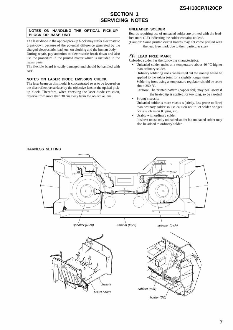
speaker (R-ch) speaker (L-ch)cabinet (front)
cabinet (rear)chassis
holder (DC)
MAIN board
HARNESS SETTING
4
ZS-H10CP/H20CPSECTION 2GENERAL
This section is extracted frominstruction manual.
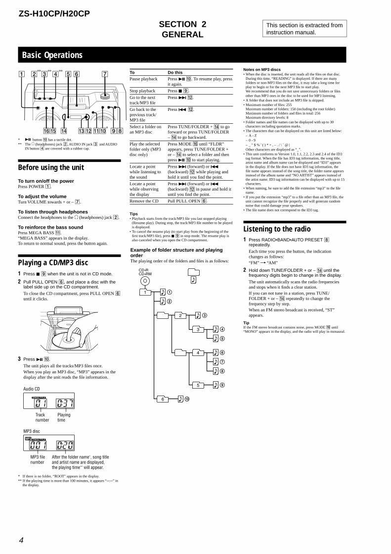
Basic Operations
* button has a tactile dot.** The (headphones) jack , AUDIO IN jack and AUDIO
IN button are covered with a rubber cap.
Before using the unit
To turn on/off the powerPress POWER .
To adjust the volumeTurn VOLUME towards + or – .
To listen through headphonesConnect the headphones to the (headphones) jack .
To reinforce the bass soundPress MEGA BASS .“MEGA BASS” appears in the display.To return to normal sound, press the button again.
Playing a CD/MP3 disc1 Press when the unit is not in CD mode.
2 Pull PULL OPEN , and place a disc with the label side up on the CD compartment.
To close the CD compartment, press PULL OPEN until it clicks.
3 Press .
The unit plays all the tracks/MP3 files once.When you play an MP3 disc, “MP3” appears in the display after the unit reads the file information.
Audio CD
Track number
Playing time
MP3 disc
MP3 file number
After the folder name*, song title and artist name are displayed, the playing time** will appear.
* If there is no folder, “ROOT” appears in the display.** If the playing time is more than 100 minutes, it appears “--:--” in
the display.
To Do thisPause playback Press . To resume play, press
it again.
Stop playback Press .
Go to the next track/MP3 file
Press .
Go back to the previous track/MP3 file
Press .
Select a folder on an MP3 disc
Press TUNE/FOLDER + to go forward or press TUNE/FOLDER – to go backward.
Play the selected folder only (MP3 disc only)
Press MODE until “FLDR” appears, press TUNE/FOLDER + or – to select a folder and then press to start playing.
Locate a point while listening to the sound
Press (forward) or (backward) while playing and hold it until you find the point.
Locate a point while observing the display
Press (forward) or (backward) in pause and hold it until you find the point.
Remove the CD Pull PULL OPEN .
Tips• Playback starts from the track/MP3 file you last stopped playing
(Resume play). During stop, the track/MP3 file number to be played is displayed.
• To cancel the resume play (to start play from the beginning of the first track/MP3 file), press in stop mode. The resume play is also canceled when you open the CD compartment.
Example of folder structure and playing orderThe playing order of the folders and files is as follows:
Notes on MP3 discs• When the disc is inserted, the unit reads all the files on that disc.
During this time, “READING” is displayed. If there are many folders or non-MP3 files on the disc, it may take a long time for play to begin or for the next MP3 file to start play. We recommend that you do not save unnecessary folders or files other than MP3 ones in the disc to be used for MP3 listening.
• A folder that does not include an MP3 file is skipped.• Maximum number of files: 255
Maximum number of folders: 150 (including the root folder) Maximum number of folders and files in total: 256 Maximum directory levels: 8
• Folder names and file names can be displayed with up to 30 characters including quotation marks.
• The characters that can be displayed on this unit are listed below:– A - Z– 0 - 9– _ " $ % ' ( ) * + , – . / \ ` @ |
Other characters are displayed as “_”.• This unit conforms to Version 1.0, 1.1, 2.2, 2.3 and 2.4 of the ID3
tag format. When the file has ID3 tag information, the song title, artist name and album name can be displayed and “ID3” appears in the display. If the file does not have ID3 tag information, the file name appears instead of the song title, the folder name appears instead of the album name and “NO ARTIST” appears instead of the artist name. ID3 tag information can be displayed with up to 15 characters.
• When naming, be sure to add the file extension “mp3” to the file name.
• If you put the extension “mp3” to a file other than an MP3 file, the unit cannot recognize the file properly and will generate random noise that could damage your speakers.
• The file name does not correspond to the ID3 tag.
Listening to the radio1 Press RADIO•BAND•AUTO PRESET
repeatedly.
Each time you press the button, the indication changes as follows:“FM” “AM”
2 Hold down TUNE/FOLDER + or – until the frequency digits begin to change in the display.
The unit automatically scans the radio frequencies and stops when it finds a clear station.If you can not tune in a station, press TUNE/FOLDER + or – repeatedly to change the frequency step by step.When an FM stereo broadcast is received, “ST” appears.
TipIf the FM stereo broadcast contains noise, press MODE until “MONO” appears in the display, and the radio will play in monaural.
5
ZS-H10CP/H20CP
Using the displayYou can check information about the CD using the display.
Checking information of an audio CD
To check the total track number and playing time of the CDPress while the CD is stopped, and you can check them in the display.
Total track number
Total playing time
Checking information of an MP3 disc
To check the total folder number and total file number on the CDPress while the CD is stopped, and you can check them in the display.
Total file number
Total folder number
To check file informationPress DSPL/ENTER while playing an MP3 disc. The display changes as follows:
The current file number and playing time
The song title and artist name
The album name*
* If there is no folder, “ROOT” appears.
Playing tracks/MP3 files repeatedly (Repeat Play)You can play tracks/MP3 files repeatedly in normal, shuffle or program play modes.
1 Press when the unit is not in CD mode.
2 Proceed as follows:
To repeat Do this
A single track/MP3 file
1 Press REPEAT until “ 1” appears.
2 Press or to select the track/MP3 file that you want to repeat.
3 Press .
All tracks/MP3 files on the CD
1 Press REPEAT until “ ” appears.2 Press .
A selected folder (MP3 disc only)
1 Press MODE to display “FLDR” and then press REPEAT until “ ” appears.
2 Select the folder by pressing TUNE/FOLDER + or – .
3 Press .
Tracks/MP3 files in random order
1 Start Shuffle Play (see “Playing tracks/MP3 files in random order”).
2 Press REPEAT until “SHUF” and “ ” appear.
3 Press .
Files in a selected folder in random order (MP3 disc only)
1 Start Folder Shuffle Play (see “Playing tracks/MP3 files in random order”).
2 Press REPEAT until “FLDR”, “SHUF” and “ ” appear.
3 Press .
Other Operations
Playing tracks/MP3 files in random order (Shuffle Play)You can play tracks/MP3 files in random order. When playing an MP3 disc, you can also play MP3 files in a selected folder in random order (Folder Shuffle Play).
1 Press when the unit is not in CD mode.
2 Press MODE until “SHUF” appears in the display.
When you select Folder Shuffle Play (MP3 disc only), press MODE until “FLDR” and “SHUF” appear in the display. Then press TUNE/FOLDER + or – to select a folder you want.
3 Press to start Shuffle Play.
To cancel Shuffle PlayStop play first. Then press MODE until “SHUF” disappears from the display.
Tips• During Shuffle Play, you cannot select the previous track/MP3 file
by pressing .• The resume function does not work during Shuffle Play.
Creating your own program (Program Play)You can arrange the playing order of up to 15 tracks/MP3 files on a CD.
1 Press when the unit is not in CD mode.
2 Press MODE until “PGM” appears in the display.
3 Press or then press DSPL/ENTER for the tracks you want to program in the
order you want.
For MP3 files, press TUNE/FOLDER + or – first and then press or and DSPL/ENTER
.
Audio CD
Programmed track number
Playing order
MP3 disc
Programmed file number
Playing order
4 Press to start Program Play.
To cancel Program PlayStop play first. Then press MODE until “PGM” disappears from the display.
To check the order of tracks/MP3 files before playPress DSPL/ENTER .Every time you press the button, the track/MP3 file number appears in the programmed order.
To change the current programPress once if the CD is stopped and twice if the CD is playing. The current program will be erased. Then create a new program following the programing procedure.
Presetting radio stationsYou can store radio stations into the unit’s memory. You can preset up to 30 radio stations, 20 for FM and 10 for AM in any order.
1 Press RADIO•BAND•AUTO PRESET to select the band.
2 Hold down RADIO•BAND•AUTO PRESET for 2 seconds until “AUTO” flashes in the display.
3 Press DSPL/ENTER .
The stations are stored in memory from the lower frequencies to the higher ones.
If a station cannot be preset automaticallyYou need to preset a station with a weak signal manually.
1 Press RADIO•BAND•AUTO PRESET to select the band.
2 Tune in the station you want.
3 Hold down DSPL/ENTER for 2 seconds until the preset number flashes in the display.
4 Press PRESET + or – until the preset number you want for the station flashes in the display.
5 Press DSPL/ENTER .
The new station replaces the old one.
TipThe preset radio stations remain in memory even if you unplug the AC power adaptor or remove the batteries.
Playing preset radio stations1 Press RADIO•BAND•AUTO PRESET to
select the band.
2 Press PRESET + or – to tune in the stored station.
Connecting an optional componentYou can enjoy the sound from a PC, TV, VCR, portable digital music player, etc. through the speakers of this unit.Be sure to turn off the power of each component before making any connections.For details, refer to the instruction manual of the component to be connected.
1 Connect AUDIO IN to the line output jack of the portable digital music player or other components using an audio connecting cable* (not supplied).* For a PC: use a cable which fills the connector of your PC.
For a TV or VCR: use a cable with a stereo-mini plug on one end and two phono plugs on the other end. For a portable digital music player: use a cable with a stereo-mini plug on both ends.
2 Turn the unit and the connected component on.
3 Press AUDIO IN and start playing sound on the connected component.
The sound from the connected component is output from the speakers.
NoteConnect the cables securely to avoid any malfunction.
To cancel Repeat PlayPress REPEAT until “ ” disappears from the display.
Tips • If you try to program 16 tracks/MP3 files or more, “FULL” will
appear in the display.• You can play the same program again, since the program is saved
until you open the CD compartment.• The resume function does not work during Program Play.
Programmed tracks/MP3 files
1 Program tracks/MP3 files (see “Creating your own program”).
2 Press REPEAT until “ ” and “PGM” appear.
3 Press .
ZS-H10CP/H20CP
6
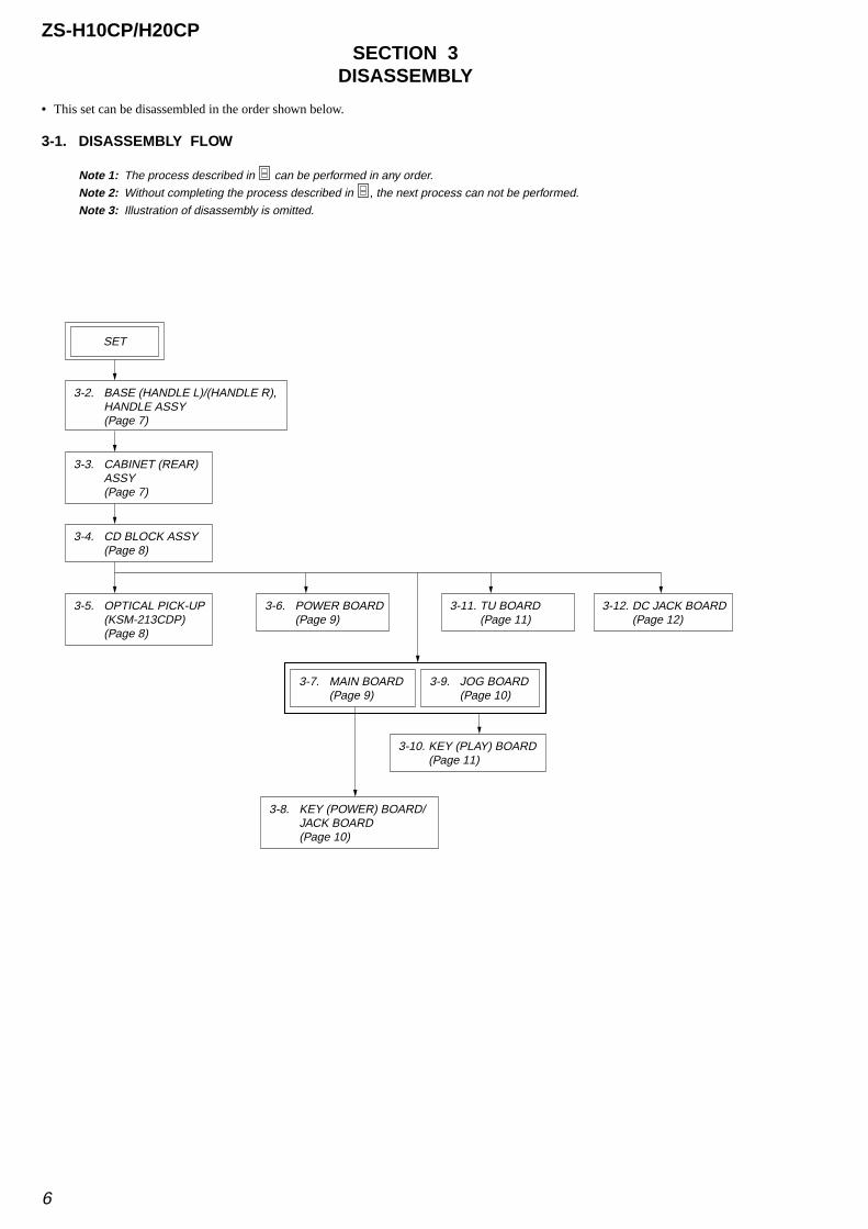
• This set can be disassembled in the order shown below.
3-1. DISASSEMBLY FLOW
Note 1: The process described in can be performed in any order.
Note 2: Without completing the process described in , the next process can not be performed.
Note 3: Illustration of disassembly is omitted.
SECTION 3DISASSEMBLY
3-5. OPTICAL PICK-UP(KSM-213CDP)(Page 8)
3-8. KEY (POWER) BOARD/JACK BOARD(Page 10)
3-7. MAIN BOARD(Page 9)
3-9. JOG BOARD(Page 10)
3-6. POWER BOARD(Page 9)
3-11. TU BOARD(Page 11)
3-12. DC JACK BOARD(Page 12)
3-4. CD BLOCK ASSY(Page 8)
3-3. CABINET (REAR) ASSY(Page 7)
3-10. KEY (PLAY) BOARD(Page 11)
3-2. BASE (HANDLE L)/(HANDLE R), HANDLE ASSY(Page 7)
SET
ZS-H10CP/H20CP
7
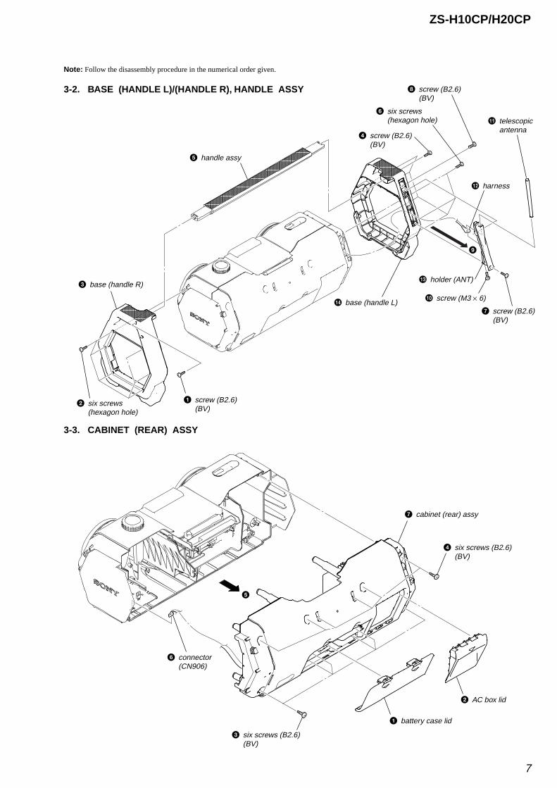
3-3. CABINET (REAR) ASSY
Note: Follow the disassembly procedure in the numerical order given.
3-2. BASE (HANDLE L)/(HANDLE R), HANDLE ASSY
5 handle assy
3 base (handle R)
2 six screws(hexagon hole)
1 screw (B2.6)(BV)
qf base (handle L)7 screw (B2.6)
(BV)
4 screw (B2.6)(BV)
6 six screws(hexagon hole)
8 screw (B2.6)(BV)
qa telescopic antenna
qs harness
9
q; screw (M3 × 6)
qd holder (ANT)
6 connector(CN906)
7 cabinet (rear) assy
5
4 six screws (B2.6)(BV)
3 six screws (B2.6)(BV)
1 battery case lid
2 AC box lid

ZS-H10CP/H20CP
8
3-4. CD BLOCK ASSY
3-5. OPTICAL PICK-UP(KSM-213CDP)
4
3 two screws (B2.6) (BV)
6 CD block assy
5 four screws (B2.6) (PWH)
1 connector (CN803)
2 flexible flat cable(23core) (CN802)
1 CD cover
3 two vibration proof rubbers(green)
2 two vibration proof rubbers(red)
6 CD board
7 optical pick-up(KSM-213CDP)
4 Remove four solders. 5 screw (BVTT2 × 6)
ZS-H10CP/H20CP
9
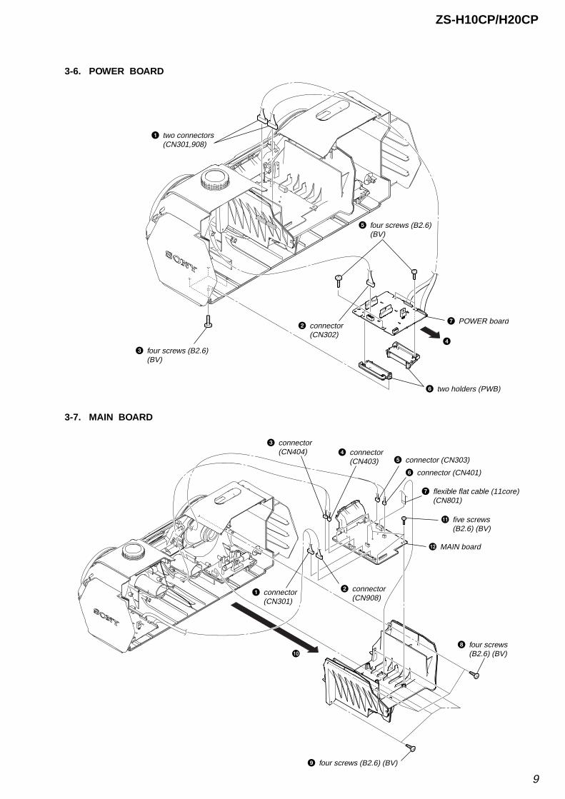
3-6. POWER BOARD
3-7. MAIN BOARD
1 two connectors(CN301,908)
3 four screws (B2.6) (BV)
5 four screws (B2.6) (BV)
2 connector(CN302)
7 POWER board
6 two holders (PWB)
4
qa five screws(B2.6) (BV)
qs MAIN board
1 connector(CN301)
2 connector(CN908)
3 connector(CN404) 4 connector
(CN403) 5 connector (CN303)
6 connector (CN401)
7 flexible flat cable (11core)(CN801)
8 four screws(B2.6) (BV)
9 four screws (B2.6) (BV)
0
ZS-H10CP/H20CP
10
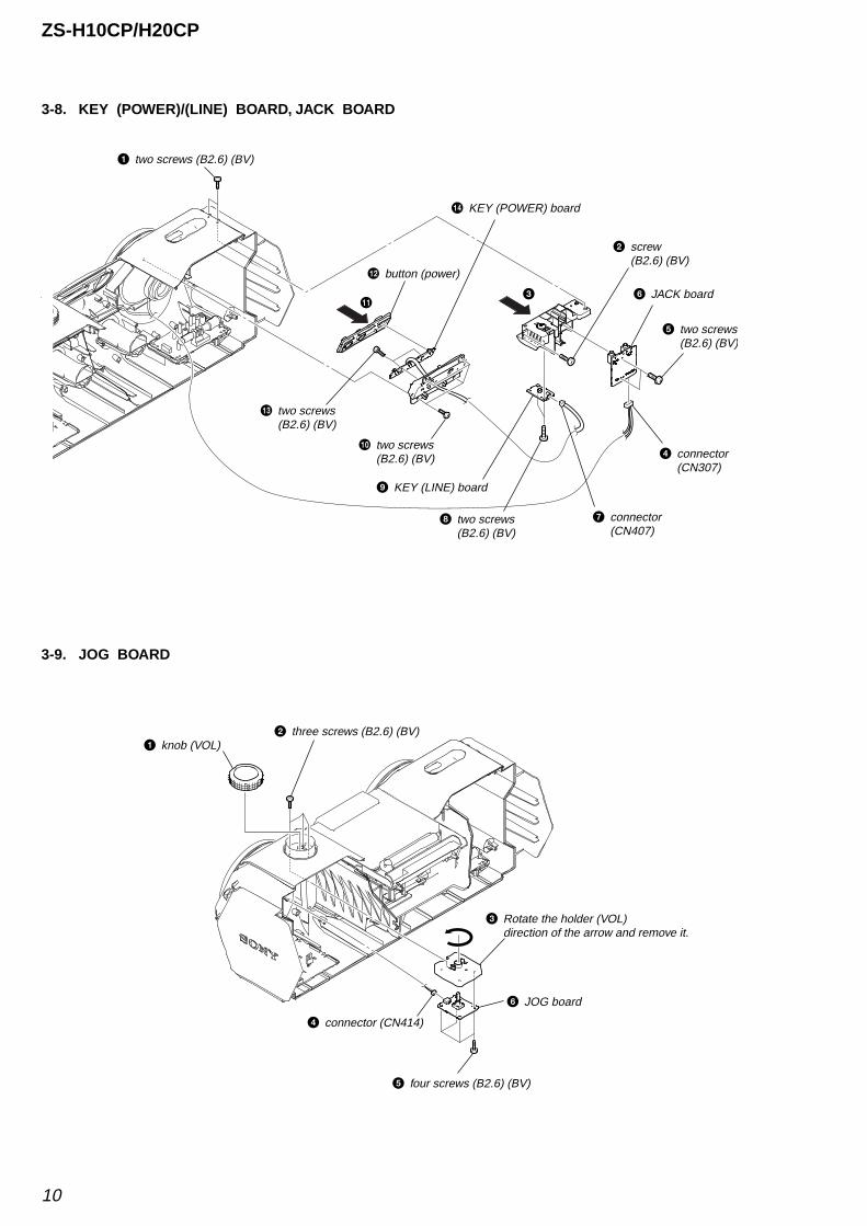
3-8. KEY (POWER)/(LINE) BOARD, JACK BOARD
3-9. JOG BOARD
1 two screws (B2.6) (BV)
2 screw(B2.6) (BV)
5 two screws(B2.6) (BV)
6 JACK board
4 connector(CN307)
7 connector(CN407)
3qa
qs button (power)
qf KEY (POWER) board
8 two screws(B2.6) (BV)
0 two screws(B2.6) (BV)
qd two screws(B2.6) (BV)
9 KEY (LINE) board
1 knob (VOL)2 three screws (B2.6) (BV)
5 four screws (B2.6) (BV)
6 JOG board
3 Rotate the holder (VOL)direction of the arrow and remove it.
4 connector (CN414)

ZS-H10CP/H20CP
11
3-10. KEY (PLAY) BOARD
3-11. TU BOARD
1 four screws (B2.6) (BV)
3 button (function)
4 two screws (B2.6) (BV)
5 KEY (PLAY) board
2
6 TU board
1 flexible flat cable (11core)(CNP1)
2 four screws (B2.6) (BV)
3 four screws(B2.6) (BV)
5 holder (PWB)
4 holder (PWB)

ZS-H10CP/H20CP
12
3-12. DC JACK BOARD
7 two screws(B2.6) (BV)
8
0 DC JACK board
6
5 four screws(B2.6) (BV)
3 connector (CN903)
1 sheet (blind D)
2 sheet (blind D)
4 connector(CN902)
9 connector(CN904)

13
ZS-H10CP/H20CP
COLD RESETProcedure:
1. In the standby mode or power on status, press three buttons of[POWER], [TUNE/FOLDER -], x simultaneously.
2. The set is reset and display “RESET”, then becomes standbystatus.
PANEL TEST MODEProcedure:
1. In the standby mode or power on status, press three buttons of[AUDIO IN], [TUNE/FOLDER +], x simultaneously.
2. When enter this mode, it turns on all segments of the LCD.3. In this mode, it displays as follows.
[AUDIO IN] button: Version display[REPEAT] button : Destination display
CHANGE OF THE AM TUNING INTERVAL(H20CP: E model only)
• The AM tuning interval can be changed to 9 kHz or 10 kHzProcedure:
1. Press the [POWER] button to turn the power on.2. Press the [RADIO, BAND, AUTO PRESET] button to select “AM”.3. Keep pressing the [DSP/ENTER] button unit “AM-**” is
displayed (2 seconds), and then keep pressing the [RADIO,
BAND, AUTO PRESET] button unit “9K STEP” or “10K STEP”is displayed (2 seconds).
4. Press the . / > button to change the AM tuning interval.
SECTION 4TEST MODE

14
ZS-H10CP/H20CPSECTION 5
ELECTRICAL ADJUSTMENTS
TUNER SECTION 0 dB=1 µV
[AM]Setting:Function: RADIOBand: AM
[FM]Setting:Function: RADIOBand: FM
• Repeat the procedures in each adjustment several times, andthe tracking adjustments should be finally done by the trimmercapacitors.
• Remove FM antenna in FM adjustment.
AM RF signal generator
30% amplitudemodulation by400 Hz signalOutput level: as low as possible
Put the lead-wireantenna close to the set.
+–
level meter
set
32 Ω
JACK Boardi jack (J302)
FM RF signalgenerator
75 kHz frequencydeviation by 1 kHzsignalOutput level: as low as possible
+–
level meter 0.01 µF
TUNER boardTP (GND)
TUNER boardTP (ANT)
set
32 Ω
JACK Boardi jack (J302)
digital voltmeter
TP (VT)TP (GND)
100 kΩTU board
AM IF ADJUSTMENT
Adjust for a maximum reading on level meter
T1 450 kHz
( ): H20CP: E model
AM FREQUENCY COVERAGE ADJUSTMENT
Adjustment Part Frequency Display Reading on Digital Voltmeter
L4 530 kHz (531 kHz) 1.0 ± 0.1 V
Confirmation1,710 kHz
5.1 ± 0.4 V (5.0 ± 0.4 V) (1,611 kHz)
( ): H20CP: E model
AM TRACKING ADJUSTMENT
Adjust for a maximum reading on level meter
L3 620 kHz (621 kHz)
CT3 1,400 kHz (1,404 kHz)
FM IF ADJUSTMENT
Adjust for a minimum reading on level meter
T2 10.7 MHz
FM FREQUENCY COVERAGE ADJUSTMENT
Adjustment Part Frequency Display Reading on Digital Voltmeter
L2 108 MHz 3.0 ± 0.2 V
Confirmation 87.5 MHz 1.3 ± 0.3 V
FM TRACKING ADJUSTMENT
Adjust for a maximum reading on level meter
L1 87.5 MHz
CT1 108 MHz
Adjustment and Connecting Location: TU board(See page 15)

ZS-H10CP/H20CP
1515ZS-H10CP/H20CP
Adjustment and Connecting Location:
L4AM Frequency Coverage Adjustment
L2FM Frequency Coverage Adjustment
AM Tracking Adjustment CT3L3
FM Tracking Adjustment
T1 AM IF Adjustment
T2 FM IF Adjustment
L1CT1
– TU Board (Component Side) –
TP(VT)
TP(GND)
TP(ANT)
– TU Board (Conductor Side) –
Checking Location:
+–
CD board
TP (RFACO)TP (VC)
oscilloscope(DC range)
Procedure :1. Connect oscilloscope to TP (RFACO) and TP (VC) on the CD
board.2. Press the [POWER] button to turn the power on.3. Set the disc (PATD-012) and press the u button to playback.4. Confirm that oscilloscope waveform is as shown in the figure
below. (eye pattern)A good eye pattern means that the diamond shape (◊) in thecenter of the waveform can be clearly distinguished.
VOLT/DIV: 200 mVTIME/DIV: 500 ns
level:0.8 to 1.4 Vp-p
CD SECTION
Note:1. CD Block is basically constructed to operate without adjustment.2. Use PATD-012 disc (Part No. 4-225-203-01) unless otherwise
indicated.3. Use an oscilloscope with more than 10 MΩ impedance.4. Clean the object lens by an applicator with neutral detergent when the
signal level is low than specified value with the following checks.5. Check the focus bias check when optical pick-up block is replaced.
FOCUS BIAS CHECK
TP(VC)
TP(RFACO)
IC201
– CD Board (Conductor Side) –
ZS-H10CP/H20CP
1616ZS-H10CP/H20CP
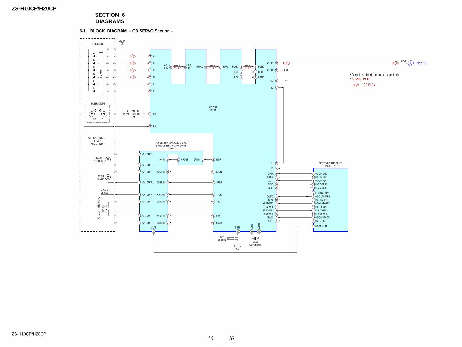
SECTION 6DIAGRAMS
6-1. BLOCK DIAGRAM – CD SERVO Section –
CD DSPIC201
CH2RIN
MUTE
2-AXISDEVICE
(TRA
CKIN
G)(F
OCUS
)
57
64
A
A+3.3V(CD)DETECTOR
A
AC_SUM
58 B65 EG_
IN 70RFACO 71 RFACI 3PCMD112AOUT1
117AOUT24 PCMDI
5BCK
55FEO
53TEO
52TEI
54FEI
6 BCKIR-CH
1LRCK 2 LRCKI
59 C
60 D
50 E
51 F
66 LD
67 PD
16 CH4OUTF
15 CH4OUTR
27 OPOUT 38 MDP
AUTOMATICPOWER CONTROL
Q321LDPD
LASER DIODE
OPTICAL PICK-UPBLOCK
(KSM-213CDP)
B
C
D
E
F
41 SFDR
42 SRDR
43 TFDR
44 TRDR
45 FFDR
46 FRDR
DATA
I-V A
MP
M401(SPINDLE)
M402(SLED)
17 CH3OUTF
18 CH3OUTR
14 CH1OUTF
13 CH1OUTR
12 CH2OUTF
11 7
20
89
SSTP
39
CH2FIN 6
CH1RIN 5
CH1FIN 4
CH3RIN 22
CH3FIN 23
CH4IN 24 OPIN+ 2
CH2OUTR
M
M
FOCUS/TRACKING COIL DRIVE,SPINDLE/SLED MOTOR DRIVE
IC402
S201(LIMIT)
D+3.3V(CD)
108
XTAO
109
XTAI
X20116.9344MHz
CLOCK 11XLAT 16SENS 20SCOR 26
DATA2 12CLK2 90
XLAT-MP3 13REQ-MP3 14
IREQ-MP3 10ACK-MP3 15
XTACN 7XRST 8
31 O-CD-CMD30 O-CD-CLK8 O-CD-XLAT
43 I-CD-SCOR
7 I-DATA-MP35 O-DATA-MP36 O-CLK-MP310 O-XLAT-MP312 O-RQ-MP327 I-RQ-MP328 I-ACK-MP326 O-CD-XTACN4 CD-XRST
11 O-M-MUTE
29 I-CD-SENS
ACD-L
SYSTEM CONTROLLERIC801 (1/2)
: CD PLAY
SIGNAL PATHR-ch is omitted due to same as L-ch.
(Page 18)
ZS-H10CP/H20CP
1717ZS-H10CP/H20CP
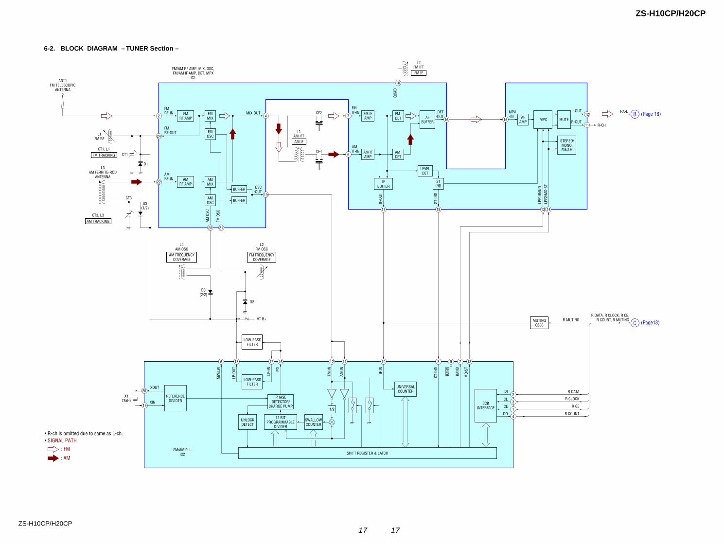
6-2. BLOCK DIAGRAM – TUNER Section –
R COUNT
2
24
4 7
20 21
FMRF AMP
FMMIX
FMOSC
FM IFAMP
IFBUFFER
AFBUFFER
AFAMP MPX MUTE
STEREO/MONO,FM/AMAM IF
AMP
FM DET
AM DET6
FMRF-IN
22AM
RF AMPAMMIX
AMRF-IN
MIX-OUT
OSC-OUT
CF2
FM/AM PLLIC2
CF4
FMRF-OUT
10
QUAD
FMIF-IN 12
1511
L-OUTMPX-IN
R-OUT
13
AMIF-IN
LPF1
/BAN
D
AM O
SC
FM O
SC
FM/AM RF AMP, MIX, OSC,FM/AM IF AMP, DET, MPX
IC1
FM FREQUENCYCOVERAGE
CT1, L1
FM TRACKING
CT3, L3
AM TRACKING
T1AM IFT
LOW-PASSFILTER
LOW-PASSFILTER
• SIGNAL PATH
: FM
: AM
X175kHz
CT3
L1FM RF
XOUT
XIN
AM IN
IF IN
ST-IN
D
LP-O
UT
LP-IN
FM IN
20
19
111218
MW
/LW
6
CT1
D1
L4AM OSC
L2FM OSC
LEVELDET
STIND
14
LPF2
/MO-
ST
AMOSC BUFFER
BUFFER
SWALLOWCOUNTER
UNIVERSALCOUNTER
CCBINTERFACE
REFERENCEDIVIDER
UNLOCKDETECT
12 BITPROGRAMMABLE
DIVIDER
PHASEDETECTOR/
CHARGE PUMP
SHIFT REGISTER & LATCH
1/2
MUTINGQ803
BAND
DI
CL
CE
DO
DET-OUT
ANT1FM TELESCOPIC
ANTENNA
PD
IF-O
UT
ST-IN
D
2
3
1
4
10 9
BAND
7
MO/
ST
13817 16
17 18
16
19
D2
VT B+
D3(1/2)
D3(2/2)
AM IF
• R-ch is omitted due to same as L-ch.
R DATA
R CLOCK
R CE
R-CH
CR MUTING
RA-L B
T2FM IFTFM IF
L3AM FERRITE-ROD
ANTENNA
R DATA, R CLOCK, R CE,R COUNT, R MUTING
AM FREQUENCYCOVERAGE
(Page 18)
(Page18)

ZS-H10CP/H20CP
1818ZS-H10CP/H20CP
6-3. BLOCK DIAGRAM – MAIN Section –
MUTINGQ102
POWER AMPIC101
POWER AMPIC201
WAKE UPSWITCH
Q402
1 –
2930
– 3
3
62 –
59
97
– 94
,89
– 6
7, 6
4, 6
3
O-TU-DATA21
O-FM/AM-SHIFT
SEG01 – SEG29
COM01 – COM04
39 –
41
I-KEY0 – I-KEY2
S401 – 404,S407 – 415
S420
SEG01 – SEG29
COM01 – COM04
2
I-WAKE-UP42
O-AM-SHIFT9
O-TU-CLK20
O-VOL-DATA33O-VOL-CLK34
O-TU-CE19I-TU-COUNT22O-TU-MUTU
R DATAR DATA, R CLOCK, R CE,R COUNT, R MUTING
R CLOCKR CER COUNTR MUTING
23
J301AUDIO IN
S419VOLUME
• SIGNAL PATH
: CD PLAY
: TUNER
: AUX IN
• R-ch is omitted due to same as L-ch.
3CD-L SELL
8
O-A-
MUT
E
3
SI
14
SC
13
O-TU-ON
POWER ONMUTING
Q811
56
I-VM 47
O-LOAD 46
+6VREGULATOR
Q953
DRY BATTERYSIZE "D"
(IEC DESIGNATION R20)6PCS. 9V
F901
RADIO 6V
D+3.3V (CD),A+3.3V (CD)
D402 – 404LCD BACK LIGHT
+1.8V (CD)
D803
D802
D303
J901
DC IN 9V
– +
TUNER B+SWITCH
Q804, 805
AMP B+
B+ 9V
B+ 6V
+3.3VREGULATOR
Q954
CD POWERON/OFF
Q955, 956
+1.8VREGULATOR
IC203EEPROMIC804
B+ 3.3V+3.3V
REGULATORIC806
RESET SIGNALGENERATOR
IC803
LIN2
RA-L
CD-L
RA-L6
LI-L
R-CH
R-CH
10
VOLTAGEDETECT
Q812DUMMY LOAD
CONTROLQ810
VOLTAGEDETECT
Q813
SYSTEM CONTROLLERIC801 (2/2)
O-CD-ON 55
I-REG 3.3V-CHK 36
POWERON/OFFQ952
O-POWER 1
B+ SWITCHQ950, 951
SHIFT CLOCKQ806, 807
LCD401LIQUID
CRYSTALDISPLAY
VT B+
+
I-REG 6.0V-CHK 38I-REG 9.0V-CHK 37
EEPROM-SCL 25EEPROM-SDA 24
I-RESET 54
(H10CP)
(H10CP)
(H20CP)
(H10CP)
(H10CP)(H20CP)
D401OPR/BATT
B(Page 17)
C(Page 17)
A(Page 16) ELECTRICALVOLUME
SOUNDCONTROL
SP101(L)
SP201(R)
J302
BOL
20
BNFL
21
16LCH
92
93X801
4.19MHzX1
X0
I-LID-OPEN45
49, 5
0 I-ENCODER +,I-ENCODER –
CD LID OPENDETECT
ROTARYENCODER
JOG ACTIVESWITCH
Q808, 809
MEGA BASSCONTROL
Q160
INPUT SELECT,ELECTRICAL VOLUME
IC301
R-CH
R-CH
R-CH
(H10CP)
+ R-CH+
i

ZS-H10CP/H20CP
1919ZS-H10CP/H20CP
• A : B+ Line.• H : adjustment for repair.• Power voltage is dc 9V and fed with regulated dc power
supply from battery terminal.• Voltages and waveforms are dc with respect to ground
under no-signal (detuned) conditions.– CD Board –no mark :CD PLAY– Other Boards –no mark : FM( ) : AM[ ] : CD PLAY
• Voltages are taken with a VOM (Input impedance 10 MΩ).Voltage variations may be noted due to normal produc-tion tolerances.
• Waveform are taken with a oscilloscope.Voltage variations may be noted due to normal produc-tion tolerances.
• Circled numbers refer to waveform.• Signal path.
F : FMf : AMJ : CD PLAYE : AUX IN
• Note for Printed Wiring Boards and Schematic Diagrams
Note on Schematic Diagram:• All capacitors are in µF unless otherwise noted. (p: pF)
50 WV or less are not indicated except for electrolyticsand tantalums.
• All resistors are in Ω and 1/4 W or less unless otherwise
specified.• f : internal component.• C : panel designation.
Note on Printed Wiring Board:• X : parts extracted from the component side.• Y : parts extracted from the conductor side.• W : indicates side identified with part number.• f : internal component.• : Pattern from the side which enables seeing.(The other layers' patterns are not indicated.)
• Circuit Boards Location
Note:The components identi-fied by mark 0 or dottedline with mark 0 are criti-cal for safety.Replace only with partnumber specified.
Note:Les composants identifiés parune marque 0 sont critiquespour la sécurité.Ne les remplacer que par unepièce por tant le numérospécifié.
BATTERY (2)board
BATTERY (1)board
DETECTION board
DC JACK board
CD Board
JOG board
KEY (LINE) boardJACK board
KEY (POWER) board
KEY (PLAY) board
TU board
POWER board
MAIN board
KEY (PRESET) board
LED board(H10CP only)
KEY (TUNE) board
ZS-H10CP/H20CP
2020ZS-H10CP/H20CP
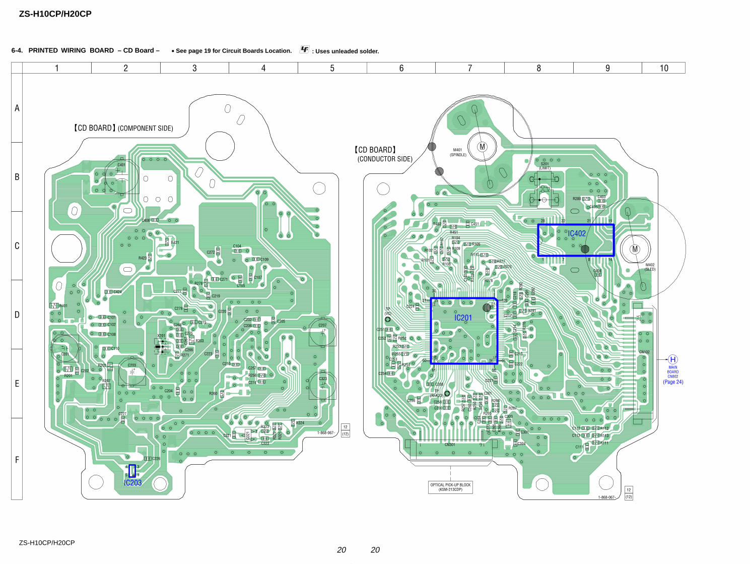
6-4. PRINTED WIRING BOARD – CD Board – • See page 19 for Circuit Boards Location. : Uses unleaded solder.
R256
C257
R260
C206C205
C322
R323
R322
R321
R324
C223
C321
C268
C267
R271
R203
C226
R201
C227
C110
C108
C102
C203
C204
C101
C274
C202
R207
C215
R202
C201
R423
R421
C424
C276
C210
Q321
C207
C266
C275
C323
C277
C406
R401
C401
C219
R276C271
C272
C104
C105
C107
C109
C232
C220
X201
IC203
C403
R257
C258
C260
C261
R258
C304
C208
R101
R265
R266
R267
C264
C265
R278
C111
C214 R2
70
C221
C292
C291
R292
R291
IC201 C217
C218
C224
R451
R102
R103
R104
R105R107
R108
R109
R110
R111
C451
IC402
C256
C251
C252
C254
C253R254
R255
R252
R253
CN301
C213
C222
C405
R113
C404
R452
C112
R275R277
C103
R112C301
C303
C273
R268
C113
CN102
C230 R250
R280
M401
M402
S201
E 1-868-067-12
(12)
CD BOARD (COMPONENT SIDE)
1
3
5
4
1-868-067-
12
(12)
CD BOARD (CONDUCTOR SIDE)
M
M
1
1 7 14
28 22
8
21 15
30
90
91
120
60
31
61
(SPINDLE)
(LIMIT)
(SLED)
HMAIN
BOARDCN802
TP(RFACO)
TP(VC)
OPTICAL PICK-UP BLOCK(KSM-213CDP)
A
B
C
D
E
F
1 2 3 4 5 6 7 8 9 10
(Page 24)
ZS-H10CP/H20CP
2121ZS-H10CP/H20CP
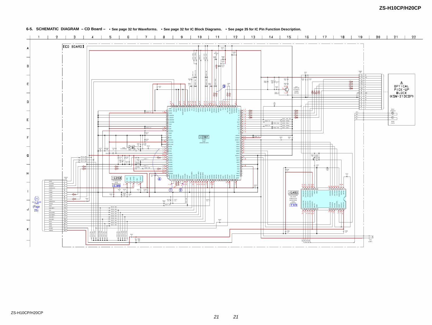
6-5. SCHEMATIC DIAGRAM – CD Board – • See page 32 for Waveforms. • See page 32 for IC Block Diagrams. • See page 35 for IC Pin Function Description.
C208
C205
R324
R101
R292
C1
10
R451
R102
R103
R104
R105
R107
R108
R109
R110
R111
R255
R253
C406
R254
R252
R2
50
R2
68
R322
R321
C2
64
CN301
C222
C213
R291C201
C219
R112
R113
C203
C1
08
C1
02
C1
01
C1
03
C1
05
C1
11
C1
04
C1
09
C1
07
C1
13
C1
12
R275
R277
R276 C271
C221
C2
73
C2
61
C2
60
R2
65
R266
R267
R2
58
C2
58
R2
60
C256
C207
C254
C253
C252
C251
C232C206
C224R
27
8
C272
C204
C218
C291
C292
C217
C202
R401
C303
C322
C321
R323
R421
C404
R207 C226
C2
65
C210
R256
C257
C323
C424
R423
C405
M402
M401
IC402
TP
C230
TP
C220
C274
R257
C304
IC201
C401
R202
C268 C215
C276
C277
R201
CN102
C266C267
R203
C275
C214
X201
R270
R271
C223
R280
R452 C451
Q321
S201
C227
IC203
C301
0.1
0.1
100k
100
100
22
0p
22k
100
100
100
100
100
100
100
100
100
1k
1k
0.1
10k
10k
1M
10
k
2.2
2.2
10
00
p
16P
0.1
0.1
10010010V
0.1
100
100
10010V
22
0p
22
p
22
p
22
p
22
p
22
0p
22
0p
22
0p
22
0p
22
p
22
p
100
100
47k 0.1
0.1
47
0p
0.0
1
0.4
7
4.7
k
1k
4.7k
22
0k
22
0p
0
0.1
100 10V
4700p
470p
4700p
470p
0.1
0.1
0.11
00
0.1
0.1
0.1
470p
470p
0.1
0.1
0
10
1
1000p
0
0
0.1
0 1
0.1
0.1
22k
0.1
10010V
0.1
10k
0.1
BA5947FM
100p
0.1
0.1
100k
1
CXD3014A-201R
22010V
0
10p 0.1
1
1
0
23P
10p5p
5p
0.1
16.9344MHz
1k
1M
0.1
0
10k 0.047
2SA2119K
1
BH18LB1WG-TR
0.1
SP
-
SP
+
SP+
SP-
SL+
SL-
SL
+
SL-
OP
IN-
OP
IN+
CH
1FIN
CH
1R
IN
CH
2FIN
CH
2R
IN
GN
D
CN
F4
PO
WV
CC
CH
2O
UT
R
CH
2O
UT
F
CH
1O
UT
R
CH
10
UT
FC
H4
OU
TR
CH
4O
UT
F
CH
3O
UT
F
CH
3O
UT
R
PO
WV
CC
MU
TE
GN
D
CH
3R
IN
CH
3FIN
CH
4IN
CH
4C
AP
A
OP
OU
T
PR
EV
CC
VR
EF
GA
IN-S
W
MIRR
DFCT
FOK
VSS
LOCK
MDP
SSTP
IOVSS1
SFDR
SRDR
TFDR
TRDR
FFDR
FRDR
IOVDD1
AVDD0
AVSS0
E
F
TEI
TEO
FEI
FEO
VC
A
B
C
D
AV
DD
4
RFD
CO
PD
SE
NS
AC
_S
UM
EG
_INLD
PD
RFC
AV
SS
4
RFA
CO
RFA
CI
AV
DD
3
BIA
S
AS
YI
AS
YO
VP
CO
VC
TL
AV
SS
3
CL
TV
FIL
O
FIL
I
PC
O
BC
KI
LR
CK
I
LR
CK
VSS
PC
MD
BC
K
VDD
IOVDD2
DOUT
TEST
IOVSS2
XVSS
XTAO
XTAI
XVDD
AVDD1
AOUT1
VREFL
AVSS1
AVSS2
VREFR
AOUT2
AVDD2
IOVDD0
IOV
SS
0
XT
AC
N
XR
ST
VS
S
VD
D
SE
NS
WFC
K
XU
GF
XP
CK
GFS
C2P
O
SC
OR
VD
D
CO
UT
PC
MD
I
CL
OK
SV
SS
SV
DD
SV
SS
SVDD
VSS
SV
DD
VD
D
VS
S
TE
ST
1
SV
SS
SVSS
SVDD
JTAGTCK
JTAGTDI
JTAGTDO
JTAGTMS
TRST
VDD
TES1
PLLVDD
PLLVSS
AC
K-M
P3
RE
Q-M
P3
IRE
Q-M
P3
SS
TB
-MP
3
XLA
T-M
P3
XL
AT
CLK2
DA
TA
DA
TA
2
T+
VC
GND
LD
PD
F+
T-
F-
VCC
D-OUT
E
D
A
B
C
F
VR
GN
D
(LIMIT)
AUTOMATIC
POWER
CONTROL
CD DSP
FOCUS/TRUCKING
(SPINDLE)
(SLED)
(VC)
(RFACO)
+1.8V REGULATOR
D-GND
L-OUT
A-GND
R-OUT
M-GND
VM(6V)
COIL DRIVE,
SPINDLE/SLED
MOTOR DRIVE
M-MUTE
XATCN
NC
VO
UT
VIN
ST
BY
DATA
CLK-MP3
DVDD(3.3V)
AVDD(3.3V)
XRST
IREQ-MP3
CLK
DATA-MP3
XLAT-MP3
REQ-MP3
ACK-MP3
XLAT
SENS
SCOR
(Page25)
ZS-H10CP/H20CP
2222ZS-H10CP/H20CP
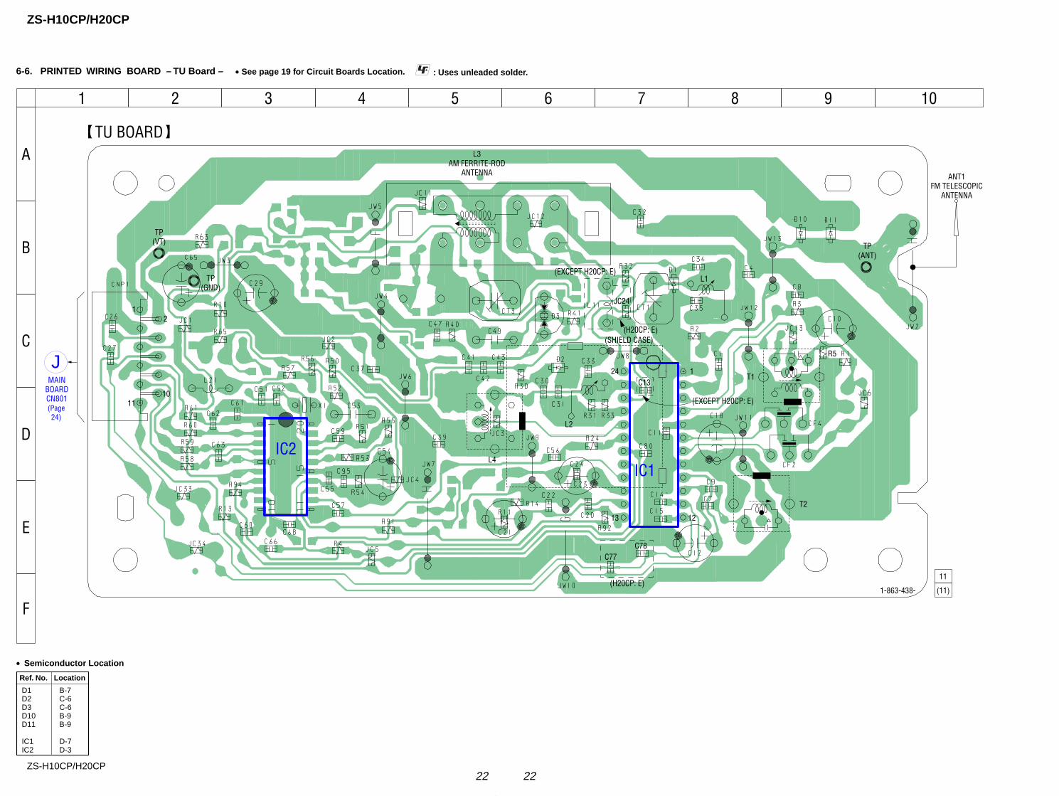
6-6. PRINTED WIRING BOARD – TU Board – • See page 19 for Circuit Boards Location. : Uses unleaded solder.
IC2IC1
TU BOARD
1-863-438-
11
(11)
L4
L3AM FERRITE-ROD
ANTENNA
L2
T2
T1
L1
(SHIELD CASE)
TP(VT)
TP(GND)
TP(ANT)
ANT1FM TELESCOPIC
ANTENNA
1 2 3 4 5 6 7 8 9 10
A
B
C
D
1
11
C13
JC24
R5
E
F
(EXCEPT H20CP: E)
C78C77
(H20CP: E)
(H20CP: E)
(EXCEPT H20CP: E)
2
10
13
24
12
1MAIN
BOARDCN801
J
(Page24)
Ref. No. Location
D1 B-7D2 C-6D3 C-6D10 B-9D11 B-9
IC1 D-7IC2 D-3
• Semiconductor Location

ZS-H10CP/H20CP
2323ZS-H10CP/H20CP
6-7. SCHEMATIC DIAGRAM – TU Board – • See page 32 for Waveforms. • See page 32 for IC Block Diagrams.
CNP1
C20
R30
R31
C34
D2C33C35
C31C30
C24 C22
C23
C37
R52 C53 C65
R91
R50
R10
C29 C27 C26
R61 R60 R59 R58
R92
C61 C62 C63
C66 C68
R94
C51 C52 R51
C59 R53 C95
C55
R54
C54 C56
C57
R65 R63
R4
R13
C1
C11C4
CF4
CF2
C8C10
C12
C9
C47 C39R40R41 C49
C41
C42
C43
R32
D1
C32
D1
1D
10
C60
C80
R24
TP
JC5
JC1
JC4
JC33
JC2
JC6R1
JC13
JC3
JC12 JC11
L2L1
L3L4
IC1
TP
ANT1
TP
T2
C18
D3
IC2
T1
CT1
CT3
R11
C21
R3
X1
R2
L11
C7
JC34
R56
L21
11P
0.1
22k
4.7kR3310k
0.01
KV1471E0.01C130.010.01
22p0.01
220p 0.1
150V
0.01
0 0.22 4.750V
220
1k
47
10010V 100p 100p
2.2k 2.2k 2.2k 2.2k
220
100p 100p 100p
100p 100p
1k
22p 10p 10k
100p 4.7k 1000p
100p
470
22010V 1000p
1000p
10k 10k
10k
1k
47p
0.11000p1000p150V
4.750V
10p
10p 0.1220k10kJC24
0 0.01
220p
100p
22p
100k
KV
14
71
E
1000p
1S
S3
55
1S
S3
55
1000p
0.01
220
(GND)
0
0
0
0
0
0470
R51K
0
0
0 0
TA2149BN
(ANT)
(VT)
22010V
KV1520NT
LC72137M-TLM
C14∗
C15∗
∗C14, 150.01 (H20CP:E)0.022 (EXCEPT H20CP:E)
C784700p
C774700p
2.2k
150V
10k
75KHz
470
5p
0
220
GND
VT
AM
OS
C
FM
OS
C
VC
C1
IF-O
UT
DE
T-O
UT
MP
X-I
N
R-O
UT
L-O
UT
ST
-IN
D
QU
AD
GN
D2
IF-I
N
AM
IF-I
N
FM
VC
C2
AG
C
LP
F1
/BA
ND
LP
F2
/MO
-ST
GN
D1
FM
RF-I
N
RF-O
UT
AM
RF-I
N
FM
OS
C-
OU
T
OU
T
MIX
-
CU
T
AM
LO
W
CE
DI
CL
DO
BA
ND
ST
-IN
D
IF I
N
XO
UT
XIN
LP
-OU
T
LP
-IN
PD
VS
S
VD
D
MO
/ST
FM
IN
AM
IN
MU
TE
AM IFT
FM
OSCFM
RF
ANTENNA AM OSC
FM/AM RF AMP,MIX,OSC,
FM/AM IF AMP,DET,MPX
FM TELESCOPIC
ANTENNA
FM/AM PLL
IFT
FM
AM FERRITE-ROD
R-MUTE
R-COUNT
R-CLOCK
R-DATA
R-CE
L-CH
RADIO 6V
R-CH
S-GND
BA
ND
MW
/LW
1µH
10µH
(EX
CEP
T H
20C
P:E
)
(EXCEPT H20CP:E)
(H20
CP
:E)
(H20CP:E)
JMAIN
BOARDCN801
AM FREQUENCYCOVERAGE
FM FREQUENCYCOVERAGE
R141k R55
10K
R57100
11
TU
(Page 25)
ZS-H10CP/H20CP
2424ZS-H10CP/H20CP
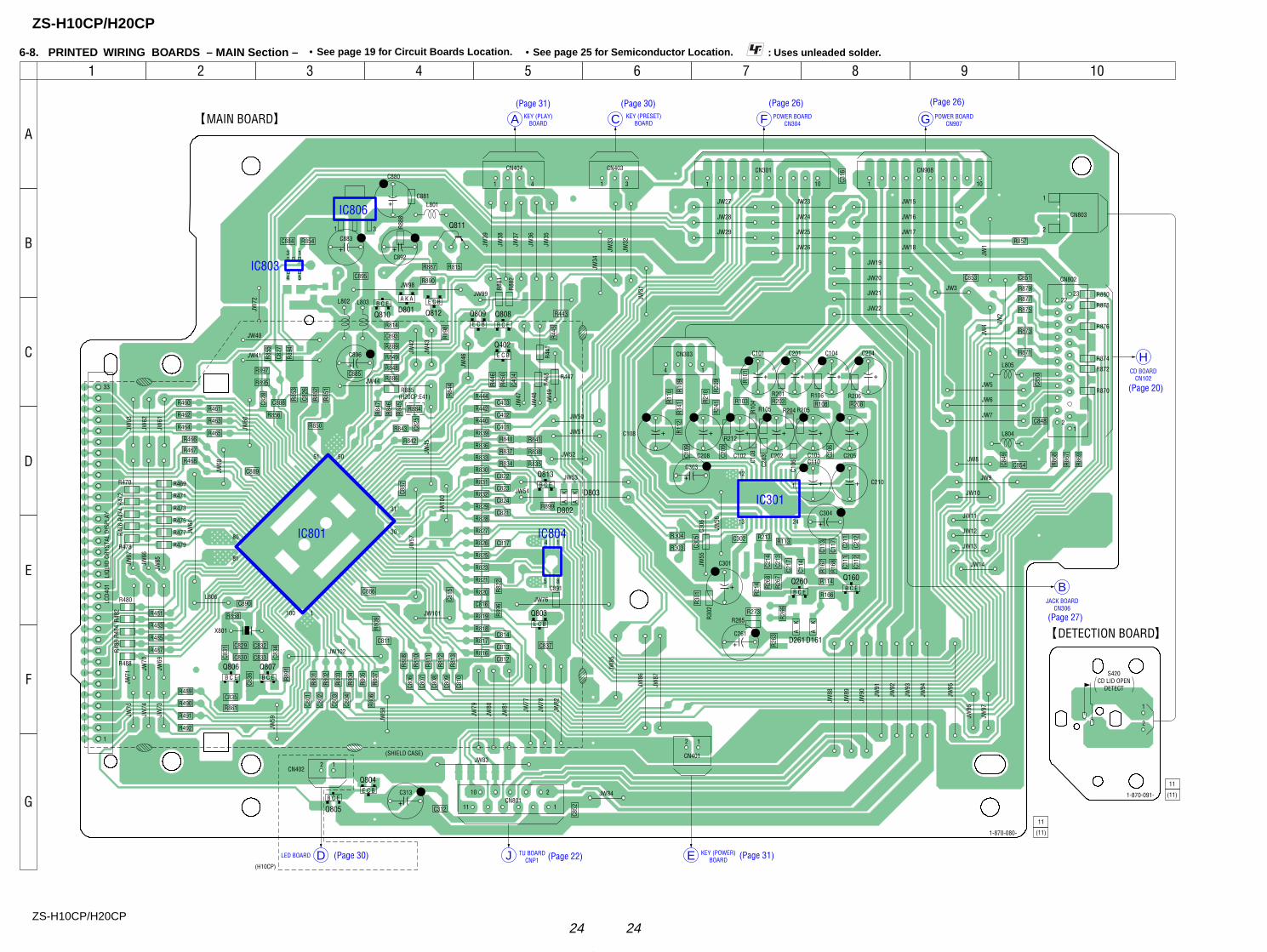
6-8. PRINTED WIRING BOARDS – MAIN Section – • See page 19 for Circuit Boards Location. : Uses unleaded solder.
Q808B C E
Q810B C E
E C B
Q809
E C B
Q402
E C BA K A
Q812D801
R885
R847
R846
R852
R851
R853
R850
R856
R460
R462
R464
R469
R471
R473
R475
R477
R470
R472
R474
R476
R478
R480
R482
R484
R486
R481 R858
C890
R483
R485
R487
R489
R490C835
C830 C833
C829 C832
C834
C836
C831
R891
R861R491
R492
R488
R479
R461
R463
R465R466
R467
R468
C889
R895
R897
C888C828 C8
26
R894
C884 R854
C895
C881
R855
C827
R845
C825
R884
R843
R842
R886C885
R848
R849
R889
C893
R814
R890
R887
R888
R815
JW60
JW61
JW62
JW63
JW67
JW66
JW70
JW71
JW69
JW65
JW68
JW75
JW74
JW73
JW59 JW
58 JW79
JW102
JW80
JW81 JW
77
JW78
JW82
JW86
JW76
JW87
JW88
JW89
JW90 JW
91
JW92
JW93
JW94
JW95
JW85
JW101
Q807B C E
Q806B C E
R801
R802
R803
R804
R805
R807
C801
C802
C803
C804
R806
Q805B C E
E C B
Q804
R808
R809
R810
R811
R812
R813
C806
C811
C886
C887
C807
C808
C809
C810
C815
C814
C837
C891
C305
C109
C209
C103
C203
C106
C206
C306
C813
C812
C312
C852
R820
C816
R822
R896
R819
R818
R817
R816
R828
R827
R826
R825
R823
R821
R836
R833
R830
R831
R832
R829
R444R844
R898
R442
R440
C403
C402
C401
C823
C822
C824
C821
C817
R839
R837
R834
R840
R838
R835
R899
R841
R448 R447
R445
R443
R446
R450
C404
R441
R882
R881
JW52
JW51
JW50
JW49
JW48
JW47
JW99
JW39
JW38
JW37
JW36
JW35
JW34
JW29
JW28
JW27
JW25
JW26
JW24
JW23
JW17
JW18
JW16
JW15
JW21
JW22
JW20
JW6
JW7
JW5
JW19
JW31
JW33
JW32
D802
KA
D803KA
JW10
0
JW45
JW64
JW41
JW40
JW44
JW98
JW42
JW43
JW46
JW72
JW57
JW53
JW54
Q813B C E
R304
R112
R141
R110
R109
R210
R241
R212
R104
R105 R204 R205
R209 R1
01
R201 R106 R206R103 R203 R108 R208
R303
E C B
Q803
R301
R302
JW55
JW56
D261
KA
D161
KA
JW84
JW83
R266
R214
R273
R114
R166
C114
R167
R168
C113R113
R213C302
C117 C2
11
C212
C111
C112
R265
R263
R268
R267
C214
C213
C217
Q160B C E
Q260B C E
JW96
JW97
JW14
JW13
JW12
JW11
JW10
JW9
JW8
JW3
JW1
JW2
JW4
C849
C850
C854
C848
R868
R867
R869
R874
R872
R870
R880
R878
R876R873
R871
C851C853
R879
R857
R877
R875
31
IC806
IC803
30
31
5051
80
81
1100
IC801
C316C880
+
C883
+
C896
+
C892+
L801
L802 L803
L806
X801
L805
L804
CN401
12
CN8011
2
11
10
33
1
LCD4
01
4 1
85
IC804
Q811
1 4
CN404
1 10
CN301
1 10
CN908
1 3
CN403
CN803
1
2
CN802
12
2322
C303
+
C261
+
C304
+
C110
+ C210+
C104
+
C204
+
C101
+
C201
+
C105
+
C205
+
C102
+
C202
+C108 +
C301
+
C208
+
4 1
CN303
CN40212
1-870-080- (11)
11
MAIN BOARD
C313
+
13
1
24
12
IC301
1
2
S420
DETECTION BOARD
1-870-091- (11)
11
A
B
C
D
E
F
G
1 2 3 4 5 6 7 8 9 10
KEY (PLAY)BOARDA KEY (PRESET)
BOARDC POWER BOARDCN304F POWER BOARD
CN907G
CD BOARDCN102
H
JACK BOARDCN306
B
3 1
4 5
KEY (POWER)BOARDELED BOARD D TU BOARD
CNP1J
LIQU
ID C
RYST
AL D
ISPL
AY
(H20CP:E41)
(H10CP)
(SHIELD CASE)
CD LID OPENDETECT
(Page 31) (Page 30) (Page 26) (Page 26)
(Page 20)
(Page 27)
(Page 30) (Page 22) (Page 31)
• See page 25 for Semiconductor Location.

ZS-H10CP/H20CP
2525ZS-H10CP/H20CP
6-9. SCHEMATIC DIAGRAM – MAIN Section – • See page 32 for Waveforms. • See page 32 for IC Block Diagrams. • See page 35 for IC Pin Function Description.
R801
R802
R803
R804
R805
R807
R809
R811
R812
C801
C802
C803
C804
C806
C807
C808
C809
C811
R813C810
C886
R816
R817
R818
R819
C812
C813
C814
C815
R820
R823
R825
R826
R827
R821
C816
C817
C821
R806
IC804
R8
30
R8
31
R8
32
R4
40
R4
42
R4
44
R4
46
R8
45
R8
46
R8
47
C887
C8
23
C8
24
C4
01
C4
02
C4
03
R849
R848
R885
R886
R4
50
R447
R448
R441
R443
R445
R8
34
R8
37
R8
40
R835 R841
CN802
C822
R842
C848
C853
C850
C854
L80410µH
L805 10µH
R867
R868
R869
R870
R871
R872
R873
R875
R878
R879
R880
CN803
R857
R844
R890
R887
R889
R898
D802C892
R850
R851
R852
R853
R855
R856
R460
R461
R462
R463
R464
R465
R466
R467
R468
R469
R470
R471
R472
R473
R474
R475
R476
R477
R478
R479
C888
R895
R897
C827
C828
R4
80
R4
81
R4
82
R4
83
R4
84
R4
85
R4
86
R4
87
R4
88
R4
89
R4
90
R4
91
R4
92
C890
R8
58
X801
Q809
R881
R882
S420
C835
C829C830
R861
C836
C834
C831
C833 C832
R815
L80247µH
R894
C896
C885
C884 C883 C895 C881 C880
R265
R273
C261
R263
L801
C3
04
C2
11
C1
11
C2
12
C1
12
C1
13
C1
17
C2
13
C2
17
R168 R167
D161
R166
Q160
R214 R267 R268
D261 R266
C302
C301
R3
03
R3
04
C303
C109
C209
C103
C203
C106
C206
C110 C210
R2
08
R1
08
C208 C108
R141
R241
R212R2
04
R2
05
R1
04
R1
05
R103R203
C105C205 C202 C102
R206
R106
R201
R101
C204
C104
C201
C101
R110
R210
R109
R209
R3
01
R3
02
C837
CN801
C312
CN908
CN301
C313
CN303
CN403
CN404
C851
R888
R884
D801
R899
R112
CN402
IC301
C114 C214
R113 R213
C316
C3
05
C3
06
R114
C852
Q805
Q804
IC806IC803
R854
C826
L8030.22µH
Q812
Q811
C893 Q810
R8
14
R8
33
R8
36
R8
39
IC801
L806
LCD401
R808
R810
R828
R829
R896
C891
C404
Q402
D803
R838
Q813
C849
Q808
R874
R876
R877
CN401
Q260
Q803
R891
Q807 Q806
R843
C825
C889
R822
1k
1k
1k
1k
1k
1k
1k
1k
1k
100p
100p
100p
100p
100p
100p
100p
100p
100p
1k100p
1
1k
1k
1k
1k
100p
100p
100p
100p
1k
1k
1k
1k
1k
1k
100p
100p
100p
220
S-24CS02AFT
1k
1k
1k
1k
1k
1k
1k
1k
1k
1k
0.01
10
0p
10
0p
0.0
1
0.0
1
0.0
1
1k
1k
10
0k
220k
220k
4.7k
4.7k
4.7k
10
k
10
k
10
k
10k 10k
23P
100p
1k
0.1
0.1
0.1
0.1
1k
1k
1k
1k
1k
1k
1k
1k
1k
1k
1k
2P
0
470k
4.7k
2.2k
10k
47k
UDZSTE-173.9B10010V
10k
10k
10k
1k
1k
1k
10k
10k
10k
10k
10k
10k
10k
10k
10k
10k
10k
10k
10k
10k
10k
10k
10k
10k
10k
10k
0.01
22k
47k
100p
100p
10
k
10
k
10
k
10
k
10
k
10
k
10
k
10
k
10
k
10
k
10
k
10
k
10
k
0.1
1k
4.19MHz
RT1N144C-TP-1
10k
10k
0.01
47p3p
10k
0.01
47p
47p
3p 47p
100k
0
0.01
22010V
0.01 10010V
0.01 0.01 100 10µH16V
470k
47k
150V
4.7k
0.4
75
0V
10
00
p
10
00
p
47
0p
47
0p
0.0
47
0.0
47
0.0
47
0.0
47
22k 4.7k
1SS355TE-17
1k
2SC3052EF-T1-LEF
220k 4.7k 22k
1SS355TE-17 1k
0.1
10010V
1k
1k
4710V
100p
100p
1000p
1000p
1000p
1000p
4.750V
4.750V
22
0k
22
0k
4.7k
4.7k 22k
10
k
10
k
10
k
10
k
100100
4.750V
4.750V
4.750V
4.750V
1k
1k
10k
10k
10k
10k
22k
22k
10
0
10
0
100p
11P
0.01
10P
10P
22010V
4P
3P
4P
0.1
220
47k
MC2838
10k
22k
2P
BD3870FS-E2
0.22 0.22
470k 470k
0.01
10
0p
10
0p
220k
0.1
RT1N144C-TP-1
RT1P144C-TP-1
XC6202P332FRS-80828CNMC
100k
100p
2SA1235
KTA1271
0.01 2SC3052EF-T1-LEF4.7
k
0 0 0
MB90802NPF-G-117E1
220
220
220
220
22k
0.1
0.01
2SA1235
UDZSTE-177.5B
47k
RT1N141C-TP-1
0.1
RT1P144C-TP-1
2.2k
2.2k
2.2k
2P
2SC3052EF-T1-LEF
RT1N144C-TP-1
10k
2SC3052EF-T1-LEF
2SC3052EF-T1-LEF
1k
100p
0.1
47k
XRST
DATA-MP3
CLK-MP3
XLAT-CD
XLAT-MP3
STBY-MP3
REQ-MP3
ACK
SENS
CLK
E-SDA
E-SCL
R COUNT
R DATA
R CLOCK
R CE
R MUTE
CMD
SCOR
CMD
KEY0
KEY1
KEY2
V-D
AT
A
V-C
LK
CD-ON
TU-ON
SEG14
SEG15
SEG16
SEG17
SEG18
SEG19
SEG20
SEG21
SEG22
SEG23
SEG24
SEG25
SEG26
SEG27
SEG28
SEG29
COM01
COM02
COM03
COM04
SCOR
SENS
XLAT-CD
ACK
REQ-MP3
XLAT-MP3
DATA-MP3
CLK
XRST
XTACNS
EG
01
SE
G0
2
SE
G0
3
SE
G0
4
SE
G0
5
SE
G0
6
SE
G0
7
SE
G0
8
SE
G0
9
SE
G1
0
SE
G1
1
SEG
12
SE
G1
3
POWER
MUTE
SE
G0
1
SE
G0
2
SE
G0
3
SE
G0
4
SE
G0
5
SE
G0
6
SE
G0
7
SE
G0
8
SE
G0
9
SE
G1
0
SE
G1
1
SEG
12
SE
G1
3
SEG
14
SE
G1
5
SE
G1
6
SEG
17
SE
G1
8
SE
G1
9
SE
G2
0
SE
G2
1
SE
G2
2
SE
G2
3
SE
G2
4
SE
G2
5
SE
G2
6
SE
G2
7
SE
G2
8
SE
G2
9
CO
M01
CO
M0
2
CO
M0
3
49
50
LID
OP
EN
LID OPEN
49
50
KEY1
VM
CO
M0
4
V-D
AT
A
V-C
LK
R CE
R DATA
R CLOCK
R COUNT
R MUTE
CD-ON
VM
MEGA-BASS
MEGA-BASS
MUTE
TU-ON
E-SDA
E-SCL
XTACN
IREQ-MP3
IREQ-MP3
POWER
KEY0
KEY2
CD-L
CD-R
TU-L
TU-R
TU-R
TU-L
STBY-MP3
CLK-MP3
CD-L
CD-R
∗
∗
∗ ∗
∗
∗
∗
∗
O-POWER
O-FM/AM-SHIFT
O-A-MUTE
CD-XRST
O-DATA-MP3
O-CLK-MP3
I-DATA-MP3
O-CD-XLAT
O-AM-SHIFT
O-XLAT-MP3
O-M-MUTE
O-RQ-MP3
NC
NC
VCC
VSS
O-TU-CE
O-TU-CLK
O-TU-DATA
I-TU-COUNT
O-TU-MUTE
EEPROM-SDA
EEPROM-SCL
O-CD-XTACN
I-RQ-MP3
I-ACK-MP3
I-CD-SENS
O-C
D-C
MD
AV
CC
O-V
OL
-DA
TA
O-V
OL
-CL
K
AV
SS
I-K
EY
0
I-K
EY
1
I-K
EY
2
I-W
AK
E-U
P
I-C
D-S
CO
R
VS
S
I-L
ID-O
PE
N
O-L
OA
D
I-V
M
I-S
HIM
UK
E
I-R
EG
3.3
V-C
HK
I-R
EG
9.0
V-C
HK
I-R
EG
6.0
V-C
HK
I-E
NC
OD
ER
+
I-E
NC
OD
ER
-
SEG14
SEG15
SEG16
SEG17
SEG18
SEG19
SEG20
SEG21
SEG22
SEG23
SEG24
SEG25
SEG26
SEG27
VSS
VCC
SEG28
SEG29
COM01
COM02
COM03
COM04
VLCD
NC
O-TU-ON
O-CD-ON
I-RESET
NC
NC
NC
SEG
01
SEG
02
SEG
03
SEG
04
X0
X1
VS
S
VC
C
SEG
05
SEG
06
SEG
07
SEG
08
SEG
09
SE
G1
0
SE
G1
1
SEG
12
SE
G1
3
O-CD-CLK
R-MUTE
GND
VT
S-GND
R COUNT
R CLOCK
R DATA
R CE
L CH
RADIO 6V
R CH
DATA
CLK-MP3
M-MUTE
DVDD(3.3V)
D-OUT
D-GND
L-OUT
A-GND
R-OUT
AVDD(3.3V)
XTACN
XRST
IREQ-MP3
CLK
DATA-MP3
XLAT-MP3
REQ-MP3
ACK-MP3
XLAT
SENS
SCOR
M-GND
VM(6V)
LIQUID CRYSTAL DISPLAY
POWER
9V
CD-ON
6V
GND
GND
3.3V
GND
VT
GND
AGND
RCH
LCH
6V
AGC
MUTE
MEGA-BASS
VM
U-VCC
U-GND
CA
P
TN
FR
TN
FL
BO
L
BN
FR
BO
R
RC
H
LC
H
VC
C
SI
SC
LIN
RIN
SE
LR
SELL
RA
-R
RA
-L
CD
-R
CD
-L
LI-
R
LI-
L
FIL
TER
GN
D
SDA
SCL
WP
VDD
GND
A2
A1
A0
∗ C101,201
0.47 50V(H20CP)
4.7 50V(H10CP)
∗ C104,204
0.1 50V(H20CP)
0.47 50V(H10CP)
4.7 50V(H10CP)
0.1 50V(H20CP)
∗ C108,208
(H20CP:E41)
∗ R885
0(EXCEPT H20CP:E41)
10k(H20CP:E41)
4.7k(H20CP:E41)
0(EXCEPT H20CP:E41)
∗ R886
(H10CP)
BN
FL
ELECTRICAL
VOLUME
INPUT
SELECT,
Q160,260
MEGA BASS CONTROL
MUTING
+3.3V
REGULATOR
RESET SIGNAL
GENERATORRES
ET
VC
C
GN
D
O G I
Q804,805
TUNER B+ SWITCH
VOLTAGE DETECT
POWER ON
MUTING
DUMMY LOAD CONTROL
MD0
MD1
MD2
SYSTEM CONTROLLER
Q806,807
SHIFT CLOCK
MEGA BASS
NC
EEPROM
WAKE UP SWITCH
VOLTAGE DETECT
Q808,809
JOG ACTIVE SWITCH
1
2
CD LID OPEN
DETECT
NC
NC
(Page29)
(Page21)
(Page 28)
(Page 29)
(Page 29)
(Page 29)
(Page28)
(Page28)
(Page23)
Ref. No. LocationRef. No. Location
D161 E-8D261 E-7D801 C-4D802 D-5D803 D-5
IC301 D-7IC801 E-3IC803 B-3
• Semiconductor Location
Ref. No. Location
IC804 E-5IC806 B-3
Q160 E-8Q260 E-7Q402 C-5Q803 E-5Q804 G-4Q805 G-3
Q806 F-2Q807 F-3Q808 C-5Q809 C-5Q810 C-4Q811 B-4Q812 C-4Q813 D-5
ZS-H10CP/H20CP
2626ZS-H10CP/H20CP
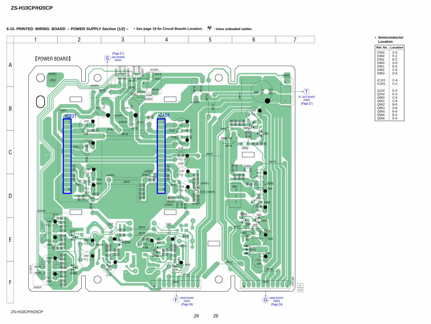
6-10. PRINTED WIRING BOARD – POWER SUPPLY Section (1/2) – • See page 19 for Circuit Boards Location. : Uses unleaded solder.
Q955
BC
E
R963
R965
C958
C956
C954
C960
R128R308
R132
R131
C134
C126
R239
R238
C227
C228
C130
C131
R130
R309
R137
R136
C138
C310
C136
R126
R129
R307
R122
JC313
R135
R156
JC304
R149 R134
R133
R157
R158
R127
C122
R964
R960
R959
R962
R310
R955R954
R957R956
R958
R950
C951
R951
R952
R953
R311
R961
D951AK
D953A K
D303A K
D952K A
D950AK
EC
B Q956
EC
B Q951
EC
BQ952
EC
B
Q102
Q202
BC
E
D361
KA
K
D360
KA
K
R227
C222
R220
R226
R229
R222
R314
R228
R161
R160
C160
R162
C260
R262
R261
R260
R270
R269
C265
R271R272
R172
C165
R171
R233
R234
R235
R230
C238R237
R170
R169
C226
C230
C231
C236
JC31
2
JC31
1
JC31
0
JC30
9
JC305 JC306
JC315
JC314
R236
C234
R231
1
5
CN906
C952+
C950
+
Q950
C137+
C135
+
C309+
C132+
C133+
C957
+
C959
+
C961
+
C308
+
C216
+
C362+
C361+
C225
+
C125
+
C116
+
C162
+
C262+
C264
+
C164+
C233
+
C232+
C235
+
C237+
C241+
C141
+
JW13
4
JW11
4
JW11
3
JW11
1
JW11
2
1 6
CN302JW133JW132
JW131
JW130
JW127
JW129
IC2011
15
IC1011
15
JW115
JW110
JW124
JW123
JW120
CN304
110
CN907
110
JW12
6
JW118
JW119
JW117
Q954
C311+
C955
+
POWER BOARD
Q953
1-87
0-08
1-(11)
11
JW12
8
JW139
JW138
JW116
R120
A
B
C
D
E
F
1 2 3 4 5 6 7
LP901
JACK BOARDCN305S
(H10CP)
(H10CP)
DC JACK BOARDCN905
T
B
C
E
E
BC
MAIN BOARDCN908GMAIN BOARD
CN301F
(H10CP)
(H20CP)
(H10CP)(H10CP)
(H10CP)
(H20CP)
(H10CP)
(H10CP)
(H20CP)
(H20CP)
(H20CP)
(H20CP)
(H10
CP)
(H10CP)
(H20CP)
(H10
CP)
(H20
CP)
(H10CP)
(H20
CP)
(H20CP)
(H20CP)
(H10CP)
(Page 27)
(Page 27)
(Page 24) (Page 24)
• SemiconductorLocation
Ref. No. Location
D303 C-6D360 F-2D361 E-2D950 D-6D951 E-6D952 C-6D953 D-6
IC101 C-4IC201 C-2
Q102 E-4Q202 E-3Q950 C-5Q951 C-6Q952 B-6Q953 D-6Q954 E-6Q955 E-6Q956 E-6
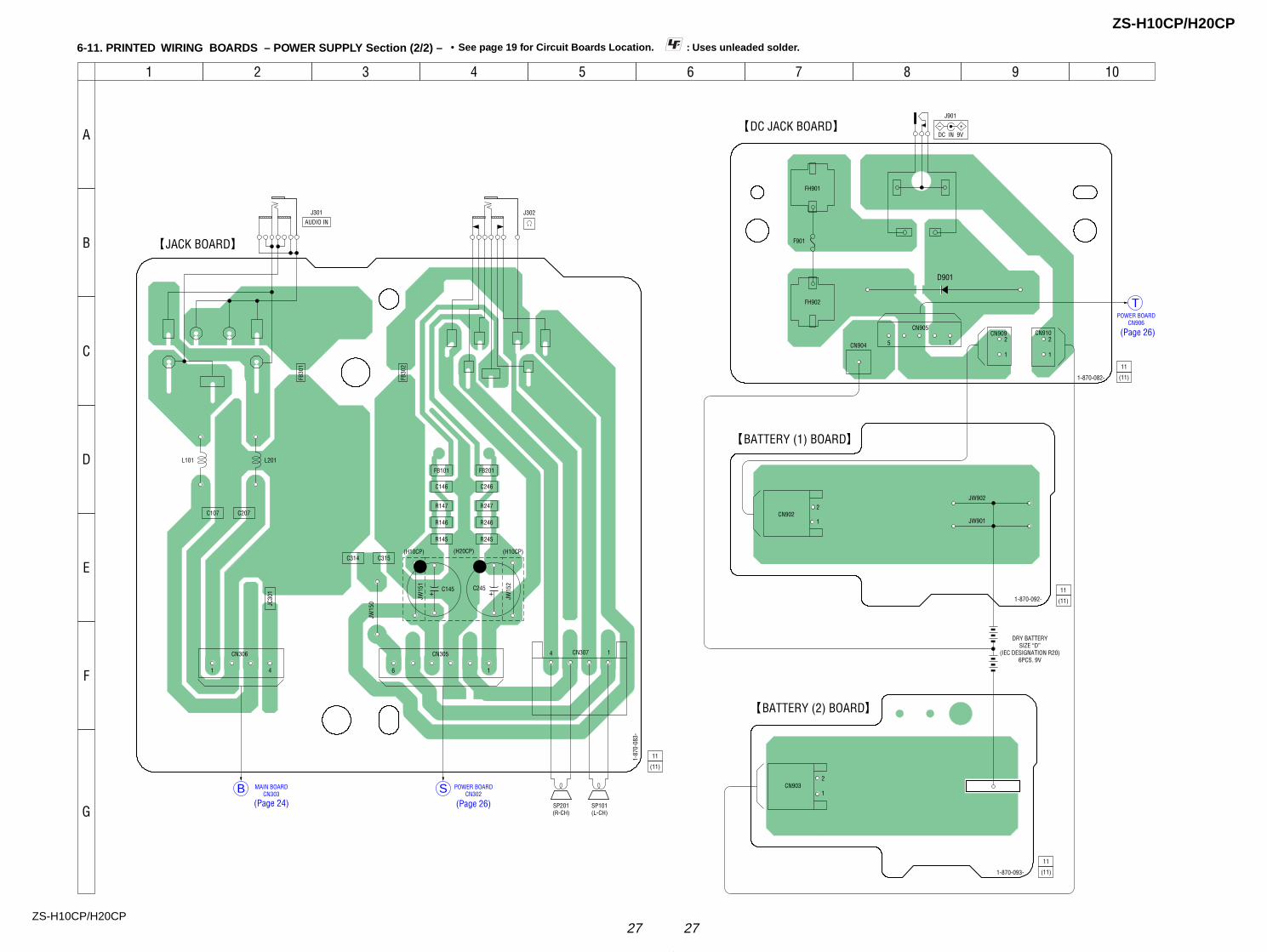
ZS-H10CP/H20CP
2727ZS-H10CP/H20CP
6-11. PRINTED WIRING BOARDS – POWER SUPPLY Section (2/2) – • See page 19 for Circuit Boards Location. : Uses unleaded solder.
FB30
1
FB30
2
L101 L201
FB101
C146
C314
JC30
1
C315
C107 C207R147
R146
R145
FB201
C246
R247
R246
R245
C145+ C245 +
16
CN305
41
CN306 14 CN307
JW15
2
JW15
1
JW15
0
JACK BOARD
J302J301
1-87
0-08
3-
(11)
11
BATTERY (2) BOARD
1-870-093- (11)
11
1
2CN903
JW902
JW9011
2CN902
BATTERY (1) BOARD
1-870-092- (11)
11
J901
F901
D901
1
1
25
CN905
CN904
CN909
1
2CN910
DC JACK BOARD
1-870-082- (11)
11
A
B
C
D
E
F
G
1 2 3 4 5 6 7 8 9 10
FH901
FH902
POWER BOARDCN302SMAIN BOARD
CN303B
iAUDIO IN
SP101(L-CH)
SP201(R-CH)
(H20CP)(H10CP) (H10CP)
DRY BATTERYSIZE “D”
(IEC DESIGNATION R20)6PCS. 9V
DC IN 9V– +
POWER BOARDCN906
T
(Page 24) (Page 26)
(Page 26)

ZS-H10CP/H20CP
2828ZS-H10CP/H20CP
6-12. SCHEMATIC DIAGRAM – POWER SUPPLY Section –
C138
R137
C136
R136
C137C135R130
JW131
JW130
C133
R134
R157
C132
R133
R135
R132R131
C126
R158
R156
R149
R238 R239
C228C227
R127
R129
Q102
R128
R122
C122
C116
C237
C238
R237
C235
C236
R236
C310
R233
R234
R230
C233
C234
C226
R231
JW129
R227
R308
R228
Q202
R229
C308
C222
R222
C216
R307
JW132
JW139
R260 R261
JW138
R161 R160
JW133JW134
C262
C260 C160
R262 R162
R270 R269 R170 R169
D361
C361C362
C265R271
R272
C165R171
R172
C162
R309
R314
CN302
JW127
CN907
CN304
C960C961
R965
C958
D951
R963
R964
Q956
C957
R962
R961 R960 R959R310 R311
D303
R956
R957R958
Q951
R955C955C956
R954
D952 D953
R950R951R952R953
C952
C950
C951
CN906
CN305
C230
JW152C245
JW151
R145
R245
C145
R147 R146 R246 R247
C246C146
C315
C314
SP101
SP201
CN307
CN306
C207
C107
L20110µH
L10110µH
FB301
CN905
CN909CN904 CN910
D901
JW901 JW902
CN903
D360
Q952
CN902
JC301
FB101FB201
FB302
J301
J302
F901
J901
C164C264
C231C232
R235
C141
C241
JC305
JC306
JC314
JC315
JC309
JC310
JC312
JC311
C225
C125
C309
C134
JC313
C131C130
JC304
R126
R120
R220 R226
IC201
IC101
Q950
Q953
C954
C311
D950
Q955
C959
Q954
0.1
2.2
0.1
2.2
10010V
10010V
1k
4710V
220
470
4710V
4.7k2.2k
2200p
470
220
1k
2.2k 4.7k
1000p2200p
100k
47k
2SC5938-T112
1k
0
4700p
150V
10010V
0.1
2.2
10010V
0.1
2.2
0.1
100
220
1k
47p10V
1000p
2200p
2.2k
100k
470k
1k
2SC5938-T112
47k
4710V
4700p
0
150
1k
47k 4.7k 4.7k 47k
1050V
0.22 0.22
10k 10k
4.7k 10k 4.7k 10k
MC2836
1050V
1050V
0.2210k
0
0.2210k
0
1050V
1k
1k
6P
10P
10P
0.122010V
100
0.01
UDZSTE-173.9B
470
1k
RT1N144C-TP-1
22010V
100
1k 1k 1k1k 1k
1SS355TE-17
47k
2.2k2.2k
2SC3052EF-T1-LEF
10k47010V0.1
10k
1SS355 1SS355
2.2k2.2k2.2k2.2k
4.750V
220016V
0.01
5P
6P
100p
4710V
1k
1k
4710V
220 220 220 220
100p100p
0.1
0.1
(L-CH)
(R-CH)
4P
4P
1000p
1000p
5P
2P1P 2P
1N5402
2P
MC2836
RT1N144C-TP-1
2P
0
1050V
1050V
100p47p10V
1k
100010V
100010V
0
0
0
0
0
0
0
0
1000p
0
100p100p
0
BA5417
BA5417
KTA1273-Y-AT
2SD2394-F
0.01
22016V
UDZSTE-176.8B
RT1P144C-TP-1
22010V
2SD999
∗
∗
PR
EG
ND
2
PR
EG
ND
1
FIL
TER
ST
BY
VC
C
NC
PO
WER
GN
D
BS
R
BS
L
NC
BS
L
VC
C
BS
R
GN
DP
OW
ER
ST
BY
FIL
TER
PR
EG
ND
1
PR
EG
ND
2
(H20CP)
(H10CP)
(H20CP)
(H10CP)
(H20CP)
(H10CP)
(H10CP)
(H10CP)
(H20C
P)
(H10C
P)
(H10CP)
∗R133
∗R135
0(H10CP)
1k(H20CP)
47 10V(H10CP)
100 10V(H20CP)
(H10CP)
100
(H20CP)
0
(H10CP)
4.7k(H10CP)
2.2k(H20CP)
2.2k(H10CP)
1k(H20CP)
4.7k(H10CP)
2.2k(H20CP) 1k(H20CP)
2.2k(H10CP)
(H10CP)
(H10CP)
(H10CP)
(H20CP)
(H20CP)
(H10CP) (H10CP)
AGND
RCH
LCH
6V
AGC
MUTE
MEGA-BASS
VM
U-VCC
U-GND
POWER
9V
CD-ON
6V
GND
GND
3.3V
GND
VT
GND
(H10CP)(H20CP)(H10CP)
2.5A 125V(H10CP)
5A 125V(H20CP:MX)
(H20CP)
(H20CP)
2.2 50V(H10CP)
1 50V(H20CP)
2.2 50V(H10CP)
1 50V(H20CP)
AUDIO IN
DC IN 9V
DRY BATTERY
SIZE"D"
(IEC DESIGNATION R20)
6PCS. 9V
MUTING
MUTING
POWER AMP
POWER AMP
Q950,951
B+ SWITCH
POWER
ON/OFF
+6V REGULATOR
Q955,956
CD POWER ON/OFF+3.3V REGULATOR
T3.15A 250V(H20CP:E)
(Page25)
(Page25)
(Page 25)
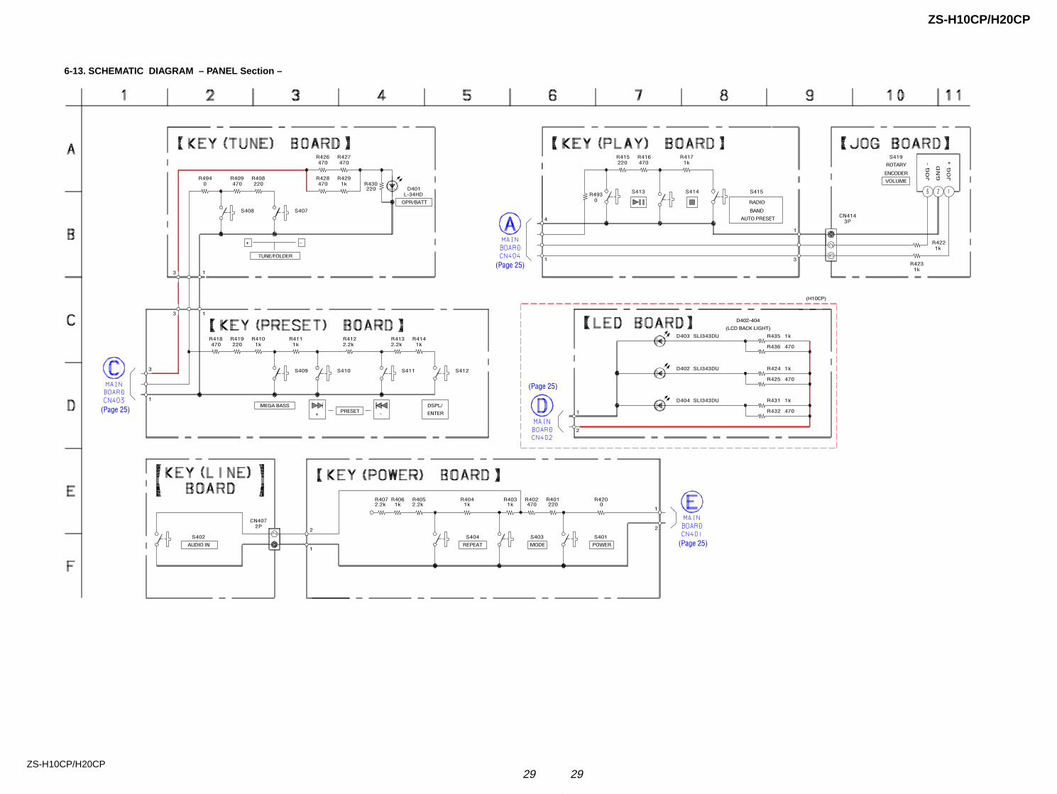
ZS-H10CP/H20CP
2929ZS-H10CP/H20CP
6-13. SCHEMATIC DIAGRAM – PANEL Section –
R401R402R403R404R405R406R407
R418 R419 R410
S410 S411 S412
R411 R412 R413 R414
R494
S408
R409 R408
S407
R428
R426 R427
R429R430
R493 S414
R415 R416 R417
R422
R423
R435
R424
R436
R425
R431
R432
CN414
S419
S415S413
D404
D402
D403
D401
S409
S402 S404 S403 S401
R420
CN407
2204701k1k2.2k1k2.2k
470 220 1k 1k 2.2k 2.2k 1k
0 470 220 470
470 470
1k220
0
220 470 1k
1k
1k
1k
1k
470
470
1k
470
3P
SLI343DU
SLI343DU
SLI343DU
L-34HD
0
2P
GN
D
JO
G -
JO
G +
(H10CP)
ROTARY
ENCODER
VOLUME
RADIO
BAND
AUTO PRESET
D402-404
OPR/BATT
+ -
TUNE/FOLDER
MEGA BASS
+ -PRESET ENTER
AUDIO IN REPEAT MODE POWER
DSPL/
(LCD BACK LIGHT)
2
1
1
2
1
3
1
1
3
3
1
2
1
4
1
3
(Page 25)
(Page 25)
(Page 25)
(Page 25)

ZS-H10CP/H20CP
3030ZS-H10CP/H20CP
6-14. PRINTED WIRING BOARDS – PANEL Section (1/2) – : Uses unleaded solder.• See page 19 for Circuit Boards Location.
R430
R427
R426
R429
R428
R494
R409 R408
S407
S408
TUNE/FOLDER+
TUNE/FOLDER–
13
KEY (TUNE) BOARD
1-870-088- (11)
11
R435
R436
R431
R432
R425
R424
12
D403 D402D404
1-870-085- (11)
11
LED BOARD
R410
R419
R418
R411
S409
S410
PRESET
S412DSPL/ENTER
S411
MEGA BASS
31
3
1
R414
R413
R412
1-870-089- (11)
11
KEY (PRESET) BOARD
.
–
>
+
A
B
C
D
E
1 2 3 4 5 6 7 8 9 10
D401OPR/BATT
D402 – 404(LCD BACK LIGHT)
MAIN BOARDCN402D
MAIN BOARDCN403C
(Page 24)
(Page 24)

ZS-H10CP/H20CP
3131ZS-H10CP/H20CP
6-15. PRINTED WIRING BOARDS – PANEL Section (2/2) – : Uses unleaded solder.• See page 19 for Circuit Boards Location.
R417
R416
R415
1 3S415
RADIOBAND
AUTO PRESETS414 S413
R493
1 4
KEY (PLAY) BOARD
1-870-087- (11)
11
1
2
CN407
S402
AUDIO IN
KEY (LINE) BOARD
1-870-090- (11)
11
1
3
CN414
R423
R422
S419ROTARY ENCODER
VOLUME
JOG BOARD
1-870-084- (11)
11
S404 S403MODEREPEAT
S401POWER
R401
R420
R402
R404
R403
R405
R406
R407 12 12
KEY (POWER) BOARD
1-870-086- (11)
11
A
B
C
D
E
F
1 2 3 4 5 6 7 8 9 10 11 12 13
MAIN BOARDCN404
A
xu
1
3
MAIN BOARDCN401
E
(Page 24)
(Page 24)
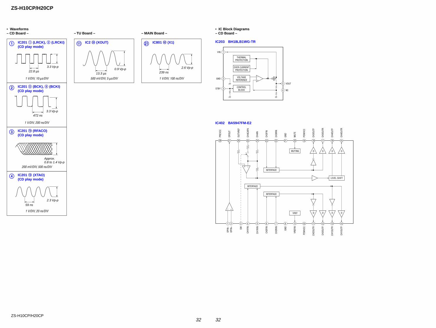
ZS-H10CP/H20CP
3232ZS-H10CP/H20CP
• Waveforms– CD Board –
3 IC201 u; (RFACO)(CD play mode)
200 mV/DIV, 500 ns/DIV
Approx.0.8 to 1.4 Vp-p
22.8 µs
3.3 Vp-p
1 IC201 1 (LRCK), 2 (LRCKI)(CD play mode)
1 V/DIV, 10 µs/DIV
2 IC201 5 (BCK), 6 (BCKI)(CD play mode)
1 V/DIV, 200 ns/DIV
472 ns3.3 Vp-p
4 IC201 <z/, (XTAO)(CD play mode)
1 V/DIV, 20 ns/DIV
59 ns
2.3 Vp-p
qa IC2 w; (XOUT)
500 mV/DIV, 5 µs/DIV
13.3 µs0.9 Vp-p
wa IC801 os (X1)
1 V/DIV, 100 ns/DIV
239 ns
2.6 Vp-p
– TU Board – – MAIN Board –• IC Block Diagrams– CD Board –
IC203 BH18LB1WG-TR
THERMALPROTECTION
VOLTAGEREFERENCE
CONTROLBLOCK
OVER CURRENTPROTECTION
VIN 1
GND 2
STBY 3NC4
VOUT5+–
1
LEVEL SHIFT
MUTING D
1516
+ –
+–
DD
1718
D
1920
VREF
2122232425262728
PREV
CC
OPOU
T
OUTV
REF
CH4C
APA
CH4I
N
CH3F
IN
CH3R
IN
GND
MUT
E
POW
VCC
CH3O
UTF
CH3O
UTR
CH4O
UTF
CH4O
UTR
OPIN
–
2
OPIN
+
INTERFACE
1413
D
1211
D
109876
CH2F
IN
CH2R
IN
GND
54
CH1F
IN
CH1R
IN
VREF
IN
POW
VCC
CH2O
UTR
CH2O
UTF
CH1O
UTR
CH1O
UTF
INTERFACE
D D
3
SW
INTERFACE
IC402 BA5947FM-E2
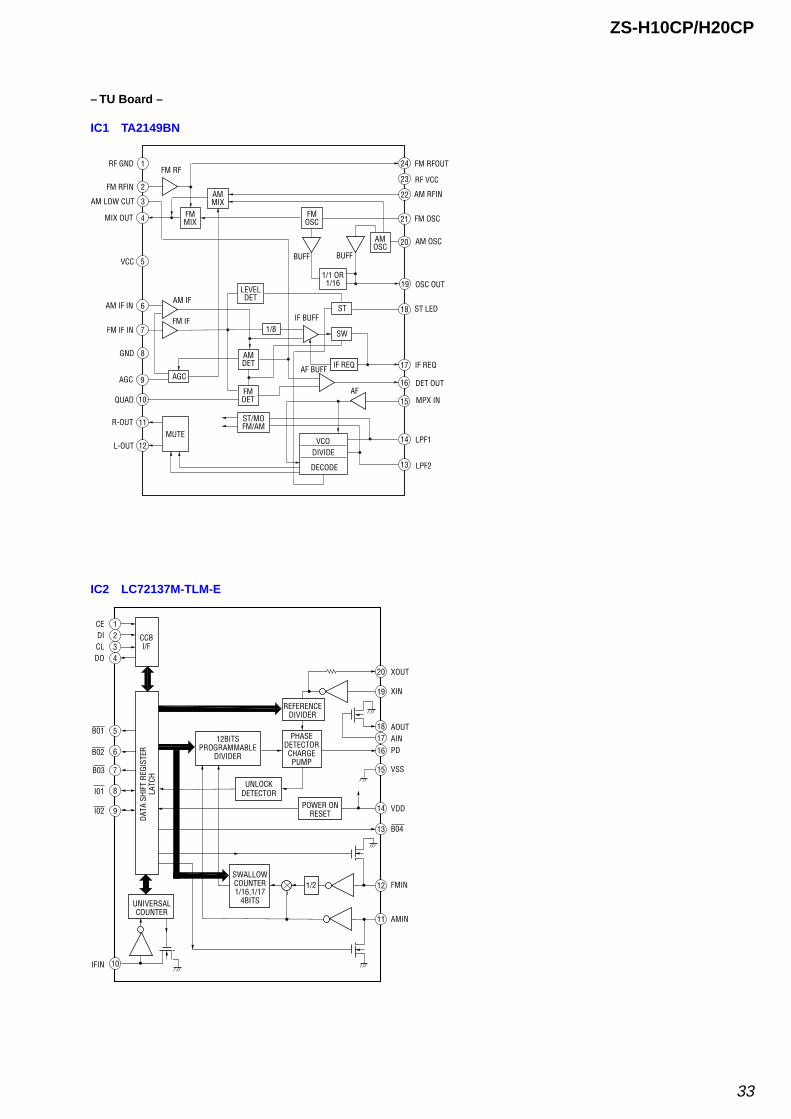
33
ZS-H10CP/H20CP
– TU Board –
IC1 TA2149BN
RF GND
3
2
1
IF REQ
AMMIX
FM RFIN
AM LOW CUT
5
4MIX OUT
VCC
AM IF IN
8
7
6
FM IF IN
GND
10
9AGC
QUAD
12
11R-OUT
L-OUT
FM RFOUT
22
23
24
20
21
17
18
19
15
16
13
14
AM RFIN
RF VCC
FM OSC
ST LED
OSC OUT
AM OSC
IF REQ
LPF1
MPX IN
DET OUT
LPF2
FMMIX
FMOSC
LEVELDET
AMDET
MUTE
FMDET
ST/MOFM/AM
AMOSC
AGC
SW
ST
1/8
BUFFBUFF
DIVIDE
DECODE
VCO
IF BUFF
AF BUFF
AF
FM RF
AM IF
FM IF
1/1 OR1/16
IC2 LC72137M-TLM-E
11
10
9
8
7
6
5
4321
12
13
14
15
16
19
20
UNLOCKDETECTOR
POWER ONRESET
UNIVERSALCOUNTER
CCBI/F
CEDICLDO
XOUT
AOUT
XIN
AINPD
VSS
VDD
B04
FMIN
AMIN
B01
B02
B03
I01
I02
IFIN
PHASEDETECTORCHARGEPUMP
REFERENCEDIVIDER
SWALLOWCOUNTER1/16,1/17
4BITS
12BITSPROGRAMMABLE
DIVIDER
DATA
SHI
FT R
EGIS
TER
LATC
H
1/2
1718
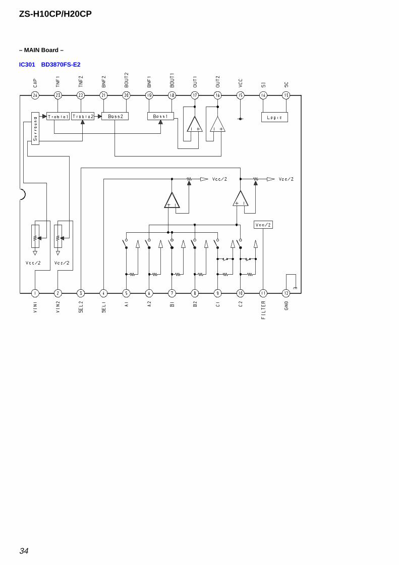
34
ZS-H10CP/H20CP
– MAIN Board –
IC301 BD3870FS-E2
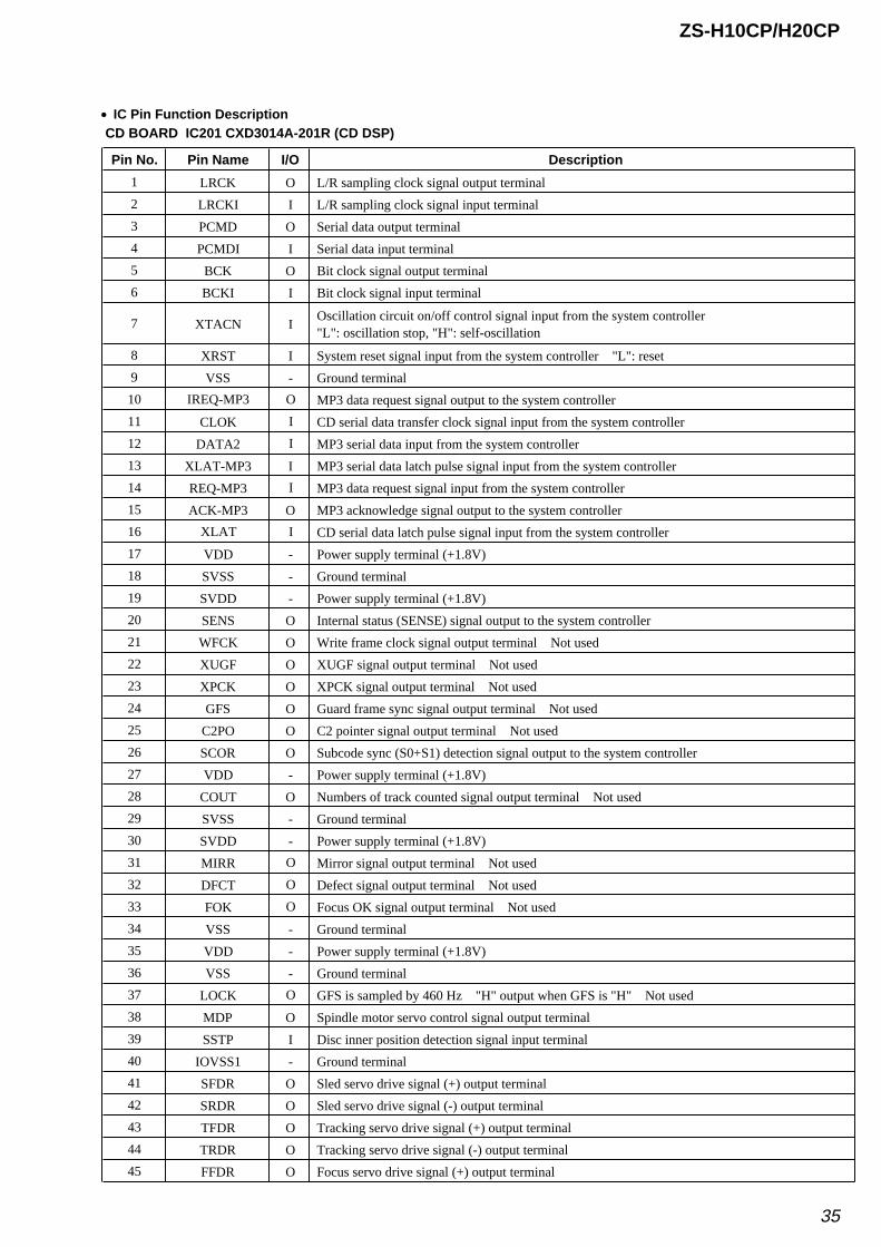
35
ZS-H10CP/H20CP
• IC Pin Function DescriptionCD BOARD IC201 CXD3014A-201R (CD DSP)
Pin No. Pin Name I/O Description
1 LRCK O L/R sampling clock signal output terminal
2 LRCKI I L/R sampling clock signal input terminal
3 PCMD O Serial data output terminal
4 PCMDI I Serial data input terminal
5 BCK O Bit clock signal output terminal
6 BCKI I Bit clock signal input terminal
7 XTACN IOscillation circuit on/off control signal input from the system controller"L": oscillation stop, "H": self-oscillation
8 XRST I System reset signal input from the system controller "L": reset
9 VSS - Ground terminal
10 IREQ-MP3 O MP3 data request signal output to the system controller
11 CLOK I CD serial data transfer clock signal input from the system controller
12 DATA2 I MP3 serial data input from the system controller
13 XLAT-MP3 I MP3 serial data latch pulse signal input from the system controller
14 REQ-MP3 I MP3 data request signal input from the system controller
15 ACK-MP3 O MP3 acknowledge signal output to the system controller
16 XLAT I CD serial data latch pulse signal input from the system controller
17 VDD - Power supply terminal (+1.8V)
18 SVSS - Ground terminal
19 SVDD - Power supply terminal (+1.8V)
20 SENS O Internal status (SENSE) signal output to the system controller
21 WFCK O Write frame clock signal output terminal Not used
22 XUGF O XUGF signal output terminal Not used
23 XPCK O XPCK signal output terminal Not used
24 GFS O Guard frame sync signal output terminal Not used
25 C2PO O C2 pointer signal output terminal Not used
26 SCOR O Subcode sync (S0+S1) detection signal output to the system controller
27 VDD - Power supply terminal (+1.8V)
28 COUT O Numbers of track counted signal output terminal Not used
29 SVSS - Ground terminal
30 SVDD - Power supply terminal (+1.8V)
31 MIRR O Mirror signal output terminal Not used
32 DFCT O Defect signal output terminal Not used
33 FOK O Focus OK signal output terminal Not used
34 VSS - Ground terminal
35 VDD - Power supply terminal (+1.8V)
36 VSS - Ground terminal
37 LOCK O GFS is sampled by 460 Hz "H" output when GFS is "H" Not used
38 MDP O Spindle motor servo control signal output terminal
39 SSTP I Disc inner position detection signal input terminal
40 IOVSS1 - Ground terminal
41 SFDR O Sled servo drive signal (+) output terminal
42 SRDR O Sled servo drive signal (-) output terminal
43 TFDR O Tracking servo drive signal (+) output terminal
44 TRDR O Tracking servo drive signal (-) output terminal
45 FFDR O Focus servo drive signal (+) output terminal
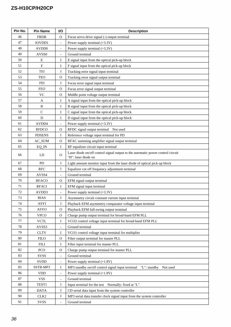
36
ZS-H10CP/H20CP
Pin No. Pin Name I/O Description
46 FRDR O Focus servo drive signal (-) output terminal
47 IOVDD1 - Power supply terminal (+3.3V)
48 AVDD0 - Power supply terminal (+3.3V)
49 AVSS0 - Ground terminal
50 E I E signal input from the optical pick-up block
51 F I F signal input from the optical pick-up block
52 TEI I Tracking error signal input terminal
53 TEO O Tracking error signal output terminal
54 FEI I Focus error signal input terminal
55 FEO O Focus error signal output terminal
56 VC O Middle point voltage output terminal
57 A I A signal input from the optical pick-up block
58 B I B signal input from the optical pick-up block
59 C I C signal input from the optical pick-up block
60 D I D signal input from the optical pick-up block
61 AVDD4 - Power supply terminal (+3.3V)
62 RFDCO O RFDC signal output terminal Not used
63 PDSENS I Reference voltage input terminal for PD
64 AC_SUM O RFAC summing amplifier signal output terminal
65 EQ_IN I RF equalizer circuit input terminal
66 LD OLaser diode on/off control signal output to the automatic power control circuit"H": laser diode on
67 PD I Light amount monitor input from the laser diode of optical pick-up block
68 RFC I Equalizer cut off frequency adjustment terminal
69 AVSS4 - Ground terminal
70 RFACO O EFM signal output terminal
71 RFACI I EFM signal input terminal
72 AVDD3 - Power supply terminal (+3.3V)
73 BIAS I Asymmetry circuit constant current input terminal
74 ASYI I Playback EFM asymmetry comparator voltage input terminal
75 ASYO O Playback EFM full-swing output terminal
76 VPCO O Charge pump output terminal for broad-band EFM PLL
77 VCTL I VCO2 control voltage input terminal for broad-band EFM PLL
78 AVSS3 - Ground terminal
79 CLTV I VCO1 control voltage input terminal for multiplier
80 FILO O Filter output terminal for master PLL
81 FILI I Filter input terminal for master PLL
82 PCO O Charge pump output terminal for master PLL
83 SVSS - Ground terminal
84 SVDD - Power supply terminal (+1.8V)
85 SSTB-MP3 I MP3 standby on/off control signal input terminal "L": standby Not used
86 VDD - Power supply terminal (+1.8V)
87 VSS - Ground terminal
88 TEST1 I Input terminal for the test Normally: fixed at "L"
89 DATA I CD serial data input from the system controller
90 CLK2 I MP3 serial data transfer clock signal input from the system controller
91 SVSS - Ground terminal
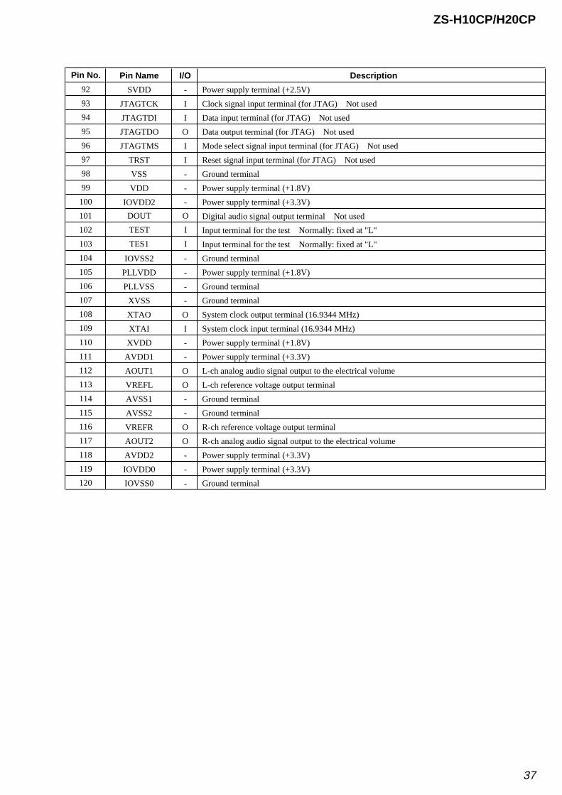
37
ZS-H10CP/H20CP
Pin No. Pin Name I/O Description
92 SVDD - Power supply terminal (+2.5V)
93 JTAGTCK I Clock signal input terminal (for JTAG) Not used
94 JTAGTDI I Data input terminal (for JTAG) Not used
95 JTAGTDO O Data output terminal (for JTAG) Not used
96 JTAGTMS I Mode select signal input terminal (for JTAG) Not used
97 TRST I Reset signal input terminal (for JTAG) Not used
98 VSS - Ground terminal
99 VDD - Power supply terminal (+1.8V)
100 IOVDD2 - Power supply terminal (+3.3V)
101 DOUT O Digital audio signal output terminal Not used
102 TEST I Input terminal for the test Normally: fixed at "L"
103 TES1 I Input terminal for the test Normally: fixed at "L"
104 IOVSS2 - Ground terminal
105 PLLVDD - Power supply terminal (+1.8V)
106 PLLVSS - Ground terminal
107 XVSS - Ground terminal
108 XTAO O System clock output terminal (16.9344 MHz)
109 XTAI I System clock input terminal (16.9344 MHz)
110 XVDD - Power supply terminal (+1.8V)
111 AVDD1 - Power supply terminal (+3.3V)
112 AOUT1 O L-ch analog audio signal output to the electrical volume
113 VREFL O L-ch reference voltage output terminal
114 AVSS1 - Ground terminal
115 AVSS2 - Ground terminal
116 VREFR O R-ch reference voltage output terminal
117 AOUT2 O R-ch analog audio signal output to the electrical volume
118 AVDD2 - Power supply terminal (+3.3V)
119 IOVDD0 - Power supply terminal (+3.3V)
120 IOVSS0 - Ground terminal

38
ZS-H10CP/H20CP
MAIN BOARD IC801 MB90802NPF-G-117E1 (SYSTEM CONTROLLER)
Pin No. Pin Name I/O Description
1 O-POWER O System power on/off control signal output terminal "H": power on
2 O-FM/AM-SHIFT O Oscillation frequency selection on/off control signal output terminal "H": selection on
3 O-A-MUTE O Audio muting on/off control signal output terminal "H": muting on
4 CD-XRST O System reset signal output to the CD DSP "L": reset
5 O-DATA-MP3 O MP3 serial data output to the CD DSP
6 O-CLK-MP3 O MP3 serial data transfer clock signal output to the CD DSP
7 I-DATA-MP3 I MP3 serial data input terminal
8 O-CD-XLAT O CD serial data latch pulse signal output to the CD DSP
9 O-AM-SHIFT O Oscillation frequency selection on/off control signal output terminal "H": selection on
10 O-XLAT-MP3 O MP3 serial data latch pulse signal output to the CD DSP
11 O-M-MUTE OMuting on/off control signal output to the motor/coil driver"L": except CD mode (muting on), "H": CD mode
12 O-RQ-MP3 O MP3 data request signal output to the CD DSP
13 NC I Not used
14 NC O Not used
15 VCC - Power supply terminal (+3.3V)
16 VSS - Ground terminal
17 MEFA BASS O Megabass on/off control signal output terminal Not used
18 NC O Not used
19 O-TU-CE O Chip enable signal output to the FM/AM PLL "L" active
20 O-TU-CLK O Serial data transfer clock signal output to the FM/AM PLL
21 O-TU-DATA O Serial data output to the FM/AM PLL
22 I-TU-COUNT I Serial count data input from the FM/AM PLL
23 O-TU-MUTE O Tuner muting on/off control signal output to the FM/AM PLL "H": muting on
24 EEPROM-SDA I/O Two-way data bus with the EEPROM
25 EEPROM-SCL O Serial data transfer clock signal output to the EEPROM
26 O-CD-XTACN OOscillation circuit on/off control signal output to the CD DSP"L": oscillation stop, "H": self-oscillation
27 I-RQ-MP3 I MP3 data request signal input from the CD DSP
28 I-ACK-MP3 I MP3 acknowledge signal input from the CD DSP
29 I-CD-SENS I Internal status (SENSE) signal input from the CD DSP
30 O-CD-CLK O CD serial data transfer clock signal output to the CD DSP
31 O-CD-CMD O CD serial data output to the CD DSP
32 AVCC - Power supply terminal (+3.3V) (for A/D converter)
33 O-VOL-DATA O Serial data output to the electrical volume
34 O-VOL-CLK O Serial data transfer clock signal output to the electrical volume
35 AVSS - Ground terminal (for A/D converter)
36 I-REG 3.3V-CHK I Input terminal for CD +3.3V power supply voltage detection
37 I-REG 9.0V-CHK I Input terminal for +9V power supply voltage detection and battery voltage detection
38 I-REG 6.0V-CHK I Input terminal for +6V power supply voltage detection
39 to 41 I-KEY0 to I-KEY2 I Front panel key input terminal (A/D input)
42 I-WAKE-UP I Wake-up signal input terminal
43 I-CD-SCOR I Subcode sync (S0+S1) detection signal input from the CD DSP
44 VSS - Ground terminal
45 I-LID-OPEN I CD lid detection signal input terminal "L": CD lid is closed, "H": CD lid is opened
46 O-LOAD O Dummy load control signal output terminal
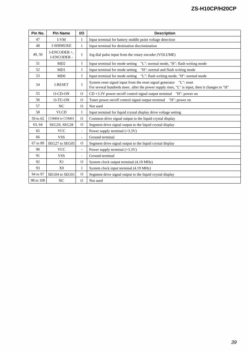
39
ZS-H10CP/H20CP
Pin No. Pin Name I/O Description
47 I-VM I Input terminal for battery middle point voltage detection
48 I-SHIMUKE I Input terminal for destination discrimination
49, 50I-ENCODER +,I-ENCODER -
I Jog dial pulse input from the rotary encoder (VOLUME)
51 MD2 I Input terminal for mode setting "L": normal mode, "H": flash writing mode
52 MD1 I Input terminal for mode setting "H": normal and flash writing mode
53 MD0 I Input terminal for mode setting "L": flash writing mode, "H": normal mode
54 I-RESET ISystem reset signal input from the reset signal generator "L": resetFor several hundreds msec. after the power supply rises, "L" is input, then it changes to "H"
55 O-CD-ON O CD +3.3V power on/off control signal output terminal "H": power on
56 O-TU-ON O Tuner power on/off control signal output terminal "H": power on
57 NC O Not used
58 VLCD I Input terminal for liquid crystal display drive voltage setting
59 to 62 COM04 to COM01 O Common drive signal output to the liquid crystal display
63, 64 SEG29, SEG28 O Segment drive signal output to the liquid crystal display
65 VCC - Power supply terminal (+3.3V)
66 VSS - Ground terminal
67 to 89 SEG27 to SEG05 O Segment drive signal output to the liquid crystal display
90 VCC - Power supply terminal (+3.3V)
91 VSS - Ground terminal
92 X1 O System clock output terminal (4.19 MHz)
93 X0 I System clock input terminal (4.19 MHz)
94 to 97 SEG04 to SEG01 O Segment drive signal output to the liquid crystal display
98 to 100 NC O Not used
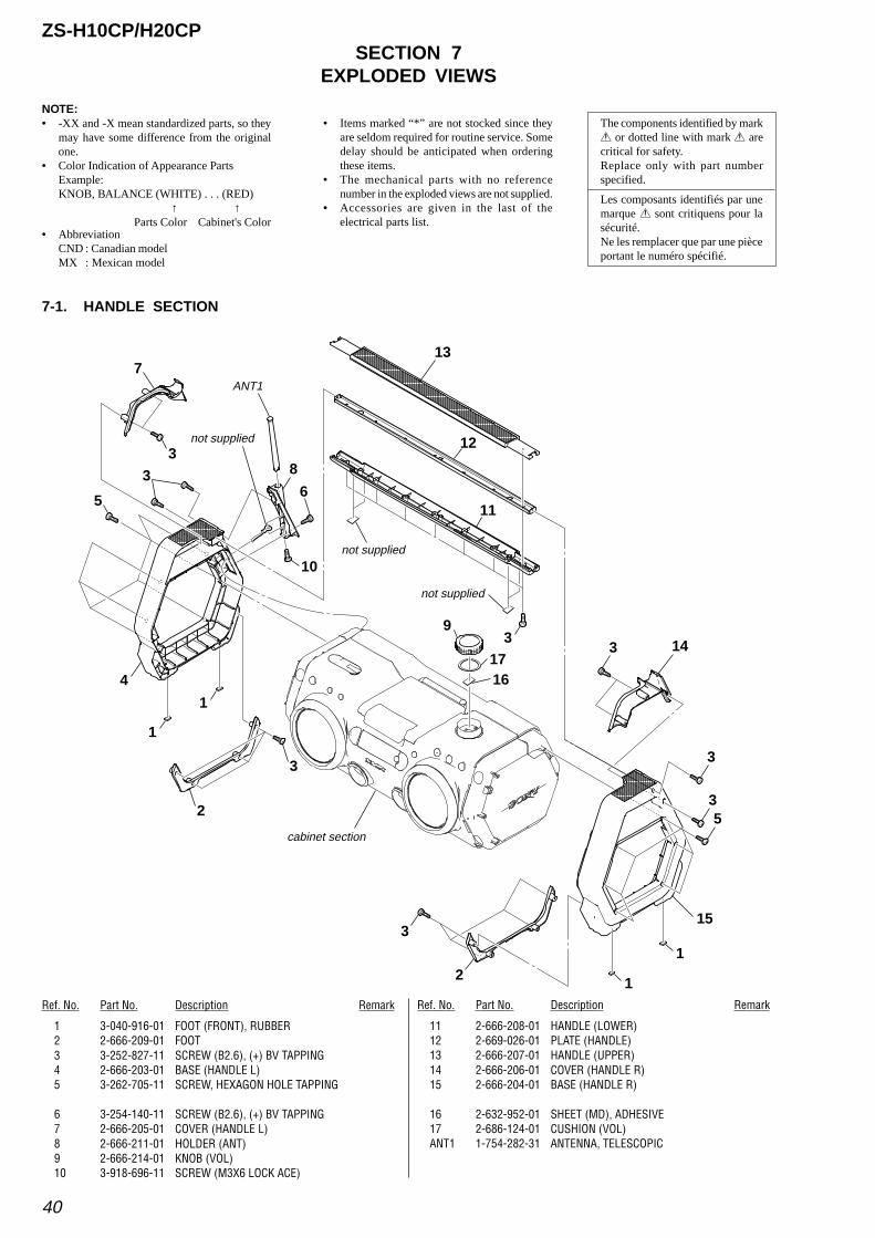
40
ZS-H10CP/H20CPSECTION 7
EXPLODED VIEWS
Ref. No. Part No. Description Remark Ref. No. Part No. Description Remark
1 3-040-916-01 FOOT (FRONT), RUBBER2 2-666-209-01 FOOT3 3-252-827-11 SCREW (B2.6), (+) BV TAPPING4 2-666-203-01 BASE (HANDLE L)5 3-262-705-11 SCREW, HEXAGON HOLE TAPPING
6 3-254-140-11 SCREW (B2.6), (+) BV TAPPING7 2-666-205-01 COVER (HANDLE L)8 2-666-211-01 HOLDER (ANT)9 2-666-214-01 KNOB (VOL)10 3-918-696-11 SCREW (M3X6 LOCK ACE)
11 2-666-208-01 HANDLE (LOWER)12 2-669-026-01 PLATE (HANDLE)13 2-666-207-01 HANDLE (UPPER)14 2-666-206-01 COVER (HANDLE R)15 2-666-204-01 BASE (HANDLE R)
16 2-632-952-01 SHEET (MD), ADHESIVE17 2-686-124-01 CUSHION (VOL)ANT1 1-754-282-31 ANTENNA, TELESCOPIC
7-1. HANDLE SECTION
• Items marked “*” are not stocked since theyare seldom required for routine service. Somedelay should be anticipated when orderingthese items.
• The mechanical parts with no referencenumber in the exploded views are not supplied.
• Accessories are given in the last of theelectrical parts list.
NOTE:• -XX and -X mean standardized parts, so they
may have some difference from the originalone.
• Color Indication of Appearance PartsExample:KNOB, BALANCE (WHITE) . . . (RED)
↑ ↑Parts Color Cabinet's Color
Les composants identifiés par unemarque 0 sont critiquens pour lasécurité.Ne les remplacer que par une pièceportant le numéro spécifié.
The components identified by mark0 or dotted line with mark 0 arecritical for safety.Replace only with part numberspecified.
• AbbreviationCND : Canadian modelMX : Mexican model
13
ANT17
3 8
3
3
35
6
10
9
1716
312
14
115
4
1
1
1
3
15
cabinet section
1
2
3
3
2
not supplied
not supplied
not supplied
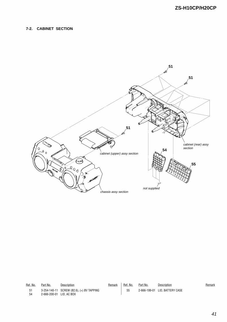
41
ZS-H10CP/H20CP
7-2. CABINET SECTION
Ref. No. Part No. Description Remark Ref. No. Part No. Description Remark
51 3-254-140-11 SCREW (B2.6), (+) BV TAPPING54 2-666-200-01 LID, AC BOX
cabinet (rear) assysection
chassis assy section
cabinet (upper) assy section
51
51
54
51
55
not supplied
55 2-666-199-01 LID, BATTERY CASE
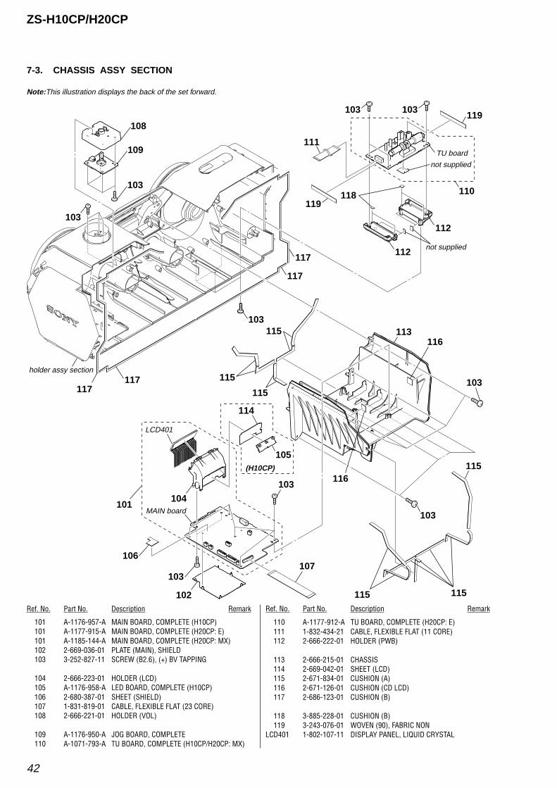
42
ZS-H10CP/H20CP
7-3. CHASSIS ASSY SECTION
Note:This illustration displays the back of the set forward.
Ref. No. Part No. Description Remark Ref. No. Part No. Description Remark
101 A-1176-957-A MAIN BOARD, COMPLETE (H10CP)101 A-1177-915-A MAIN BOARD, COMPLETE (H20CP: E)101 A-1185-144-A MAIN BOARD, COMPLETE (H20CP: MX)102 2-669-036-01 PLATE (MAIN), SHIELD103 3-252-827-11 SCREW (B2.6), (+) BV TAPPING
104 2-666-223-01 HOLDER (LCD)105 A-1176-958-A LED BOARD, COMPLETE (H10CP)106 2-680-387-01 SHEET (SHIELD)107 1-831-819-01 CABLE, FLEXIBLE FLAT (23 CORE)108 2-666-221-01 HOLDER (VOL)
109 A-1176-950-A JOG BOARD, COMPLETE110 A-1071-793-A TU BOARD, COMPLETE (H10CP/H20CP: MX)
110 A-1177-912-A TU BOARD, COMPLETE (H20CP: E)111 1-832-434-21 CABLE, FLEXIBLE FLAT (11 CORE)112 2-666-222-01 HOLDER (PWB)
113 2-666-215-01 CHASSIS114 2-669-042-01 SHEET (LCD)115 2-671-834-01 CUSHION (A)116 2-671-126-01 CUSHION (CD LCD)117 2-686-123-01 CUSHION (B)
118 3-885-228-01 CUSHION (B)119 3-243-076-01 WOVEN (90), FABRIC NON
LCD401 1-802-107-11 DISPLAY PANEL, LIQUID CRYSTAL
TU board
not supplied
holder assy section
LCD401
(H10CP)
MAIN board
108
103103
110
112
112
103
117117
117
117
103
113
103
105
104
114
101
107
109
103
103
111
118
103
103
102
not supplied
115
116
116
115
115
115 115
115
119
119
106
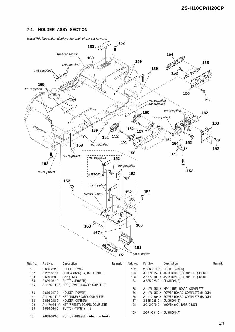
43
ZS-H10CP/H20CP
7-4. HOLDER ASSY SECTION
Note:This illustration displays the back of the set forward.
Ref. No. Part No. Description Remark Ref. No. Part No. Description Remark
151 2-666-222-01 HOLDER (PWB)152 3-252-827-11 SCREW (B2.6), (+) BV TAPPING153 2-669-029-01 CAP (LINE)154 2-669-031-01 BUTTON (POWER)155 A-1176-948-A KEY (POWER) BOARD, COMPLETE
156 2-666-217-01 HOLDER (POWER)157 A-1176-942-A KEY (TUNE) BOARD, COMPLETE158 2-666-218-01 HOLDER (CENTER)159 A-1176-944-A KEY (PRESET) BOARD, COMPLETE160 2-669-034-01 BUTTON (TUNE) (+, –)
161 2-669-033-01 BUTTON (PRESET) (>, +, –, .)
162 2-666-219-01 HOLDER (JACK)163 A-1176-952-A JACK BOARD, COMPLETE (H10CP)163 A-1177-805-A JACK BOARD, COMPLETE (H20CP)164 3-885-228-01 CUSHION (B)
165 A-1176-954-A KEY (LINE) BOARD, COMPLETE166 A-1176-959-A POWER BOARD, COMPLETE (H10CP)166 A-1177-807-A POWER BOARD, COMPLETE (H20CP)167 3-885-228-01 CUSHION (B)168 3-243-076-01 WOVEN (90), FABRIC NON
169 2-671-834-01 CUSHION (A)
163
165not supplied
not supplied
not supplied
(H20CP)
POWER board
speaker section
152153
155
162160
152157
152
156
154
152
152
152
151
166
151
152152
158
152
152
152161
152
159 164
152
152
152
167
168
168
not supplied
not supplied
not supplied
not supplied
169
169
not supplied
not supplied
not supplied
not supplied
not supplied
not supplied
169
169169
169
not supplied
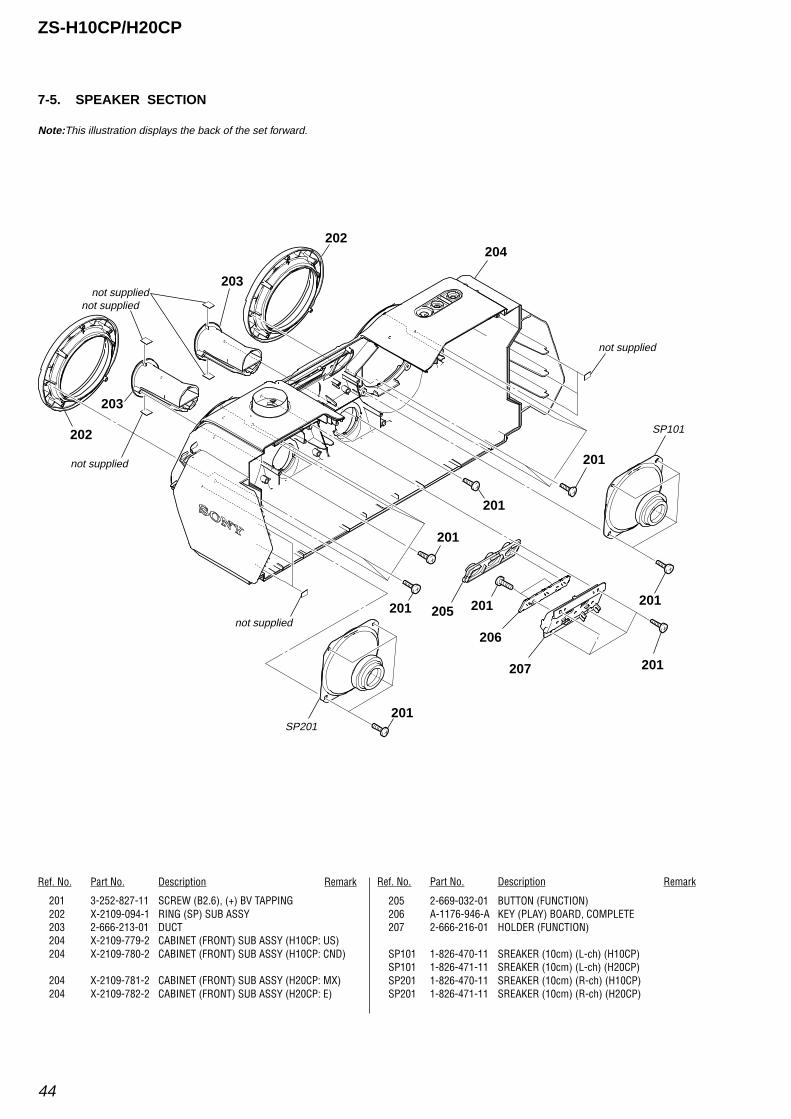
44
ZS-H10CP/H20CP
7-5. SPEAKER SECTION
Note:This illustration displays the back of the set forward.
Ref. No. Part No. Description Remark Ref. No. Part No. Description Remark
201 3-252-827-11 SCREW (B2.6), (+) BV TAPPING202 X-2109-094-1 RING (SP) SUB ASSY203 2-666-213-01 DUCT204 X-2109-779-2 CABINET (FRONT) SUB ASSY (H10CP: US)204 X-2109-780-2 CABINET (FRONT) SUB ASSY (H10CP: CND)
204 X-2109-781-2 CABINET (FRONT) SUB ASSY (H20CP: MX)204 X-2109-782-2 CABINET (FRONT) SUB ASSY (H20CP: E)
205 2-669-032-01 BUTTON (FUNCTION)206 A-1176-946-A KEY (PLAY) BOARD, COMPLETE207 2-666-216-01 HOLDER (FUNCTION)
SP101 1-826-470-11 SREAKER (10cm) (L-ch) (H10CP)SP101 1-826-471-11 SREAKER (10cm) (L-ch) (H20CP)SP201 1-826-470-11 SREAKER (10cm) (R-ch) (H10CP)SP201 1-826-471-11 SREAKER (10cm) (R-ch) (H20CP)
204
201
201
201
201207
SP101
202
202
203
203
201
206
201201
201
205
SP201
not supplied
not supplied
not suppliednot supplied
not supplied

45
ZS-H10CP/H20CP
7-6. CABINET (UPPER) ASSY SECTION
Ref. No. Part No. Description Remark Ref. No. Part No. Description Remark
251 3-252-828-01 SCREW (B2.6), (+) PWH TAPPING252 3-252-827-11 SCREW (B2.6), (+) BV TAPPING253 3-047-468-11 DAMPER254 2-669-040-01 SPRING (CD LID)255 2-666-198-01 CABINET (UPPER)
256 2-669-028-01 PACKING (CD LID)257 2-669-038-01 SHAFT (CD LID)258 3-253-143-01 SCREW (B2.6), (+) P TAPPING259 3-019-395-01 PLATE, CHUCKING260 1-452-899-11 MAGNET
261 2-669-039-01 SHAFT (BUCKLE)262 2-666-202-01 LID, CD263 2-666-224-01 PLATE (LOCK)264 2-666-210-01 BUCKLE (CD LID)265 2-669-041-01 SPRING (BUCKLE)
266 2-675-701-01 SHEET (UPPER)268 A-1176-963-A DETECTION BOARD, COMPLETE269 2-671-834-01 CUSHION (A)270 2-686-123-01 CUSHION (B)271 2-686-125-01 CUSHION (DC)
262
266
CD block assy section
251
257
265
258
268
252
264
256
263259
254
255
253
252
257
260
261
270
269
269
269
269
269
not supplied
not supplied
not supplied
271
271
not supplied
not supplied

46
ZS-H10CP/H20CP
7-7. CD BLOCK ASSY SECTION
Ref. No. Part No. Description Remark Ref. No. Part No. Description Remark
301 A-1134-279-A CD BOARD, COMPLETE302 3-931-379-21 RUBBER, VIBRATION PROOF (GREEN)
0303 8-820-126-02 OPTICAL PICK-UP (KSM-213CDP/C2NP)304 3-923-736-01 COVER, CD305 3-931-379-31 RUBBER, VIBRATION PROOF (RED)
306 1-832-404-21 CABLE, FLEXIBLE FLAT (16 CORE)S201 1-771-853-11 SWITCH, DETECTION (LIMIT)#1 7-685-853-04 SCREW +BVTT 2X6 (S)
304
305
306
301
302
302
#1
303
S201
305
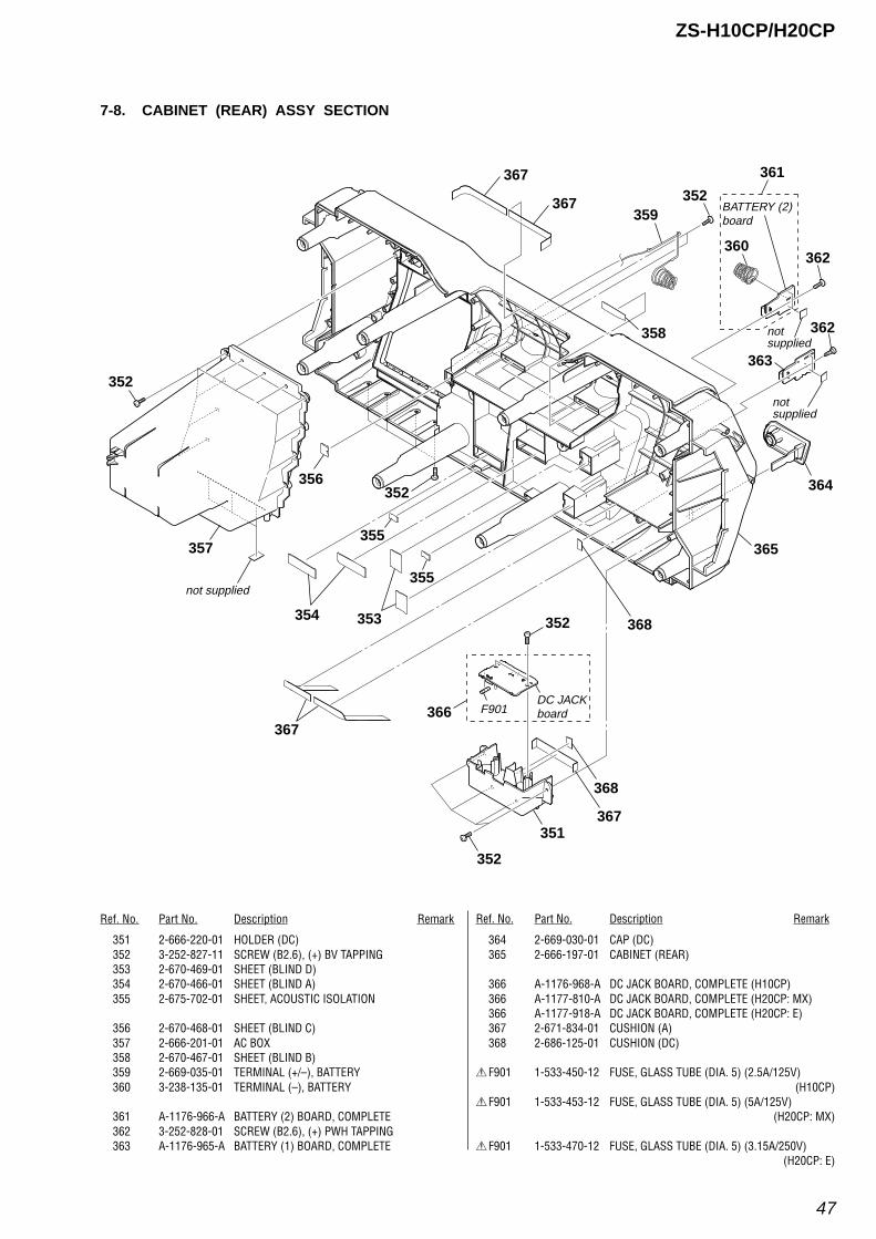
47
ZS-H10CP/H20CP
7-8. CABINET (REAR) ASSY SECTION
Ref. No. Part No. Description Remark Ref. No. Part No. Description Remark
351 2-666-220-01 HOLDER (DC)352 3-252-827-11 SCREW (B2.6), (+) BV TAPPING353 2-670-469-01 SHEET (BLIND D)354 2-670-466-01 SHEET (BLIND A)355 2-675-702-01 SHEET, ACOUSTIC ISOLATION
356 2-670-468-01 SHEET (BLIND C)357 2-666-201-01 AC BOX358 2-670-467-01 SHEET (BLIND B)359 2-669-035-01 TERMINAL (+/–), BATTERY360 3-238-135-01 TERMINAL (–), BATTERY
361 A-1176-966-A BATTERY (2) BOARD, COMPLETE362 3-252-828-01 SCREW (B2.6), (+) PWH TAPPING363 A-1176-965-A BATTERY (1) BOARD, COMPLETE
364 2-669-030-01 CAP (DC)365 2-666-197-01 CABINET (REAR)
366 A-1176-968-A DC JACK BOARD, COMPLETE (H10CP)366 A-1177-810-A DC JACK BOARD, COMPLETE (H20CP: MX)366 A-1177-918-A DC JACK BOARD, COMPLETE (H20CP: E)367 2-671-834-01 CUSHION (A)368 2-686-125-01 CUSHION (DC)
0F901 1-533-450-12 FUSE, GLASS TUBE (DIA. 5) (2.5A/125V)(H10CP)
0F901 1-533-453-12 FUSE, GLASS TUBE (DIA. 5) (5A/125V)(H20CP: MX)
0F901 1-533-470-12 FUSE, GLASS TUBE (DIA. 5) (3.15A/250V)(H20CP: E)
359
358
352
363
BATTERY (2)board
360
365
351
355
355
353
352
352
352
366
352
362
361
364
notsupplied
362
notsupplied
F901DC JACK board
356
357
354
not supplied
367
367
367
368
368
367
48
ZS-H10CP/H20CPSECTION 8
ELECTRICAL PARTS LISTBATTERY (1)
Ref. No. Part No. Description Remark Ref. No. Part No. Description Remark
A-1176-965-A BATTERY (1) BOARD, COMPLETE***************************
< CONNECTOR >
CN902 1-815-550-21 PIN, CONNECTOR (PWB) 2P************************************************************
A-1176-966-A BATTERY (2) BOARD, COMPLETE***************************
3-238-135-01 TERMINAL (–), BATTERY
< CONNECTOR >
CN903 1-815-550-11 PIN, CONNECTOR (PWB) 2P************************************************************
A-1134-279-A CD BOARD, COMPLETE*******************
< CAPACITOR >
C101 1-162-919-11 CERAMIC CHIP 22PF 5% 50VC102 1-162-919-11 CERAMIC CHIP 22PF 5% 50VC103 1-162-919-11 CERAMIC CHIP 22PF 5% 50VC104 1-164-230-11 CERAMIC CHIP 220PF 5% 50VC105 1-162-919-11 CERAMIC CHIP 22PF 5% 50V
C107 1-164-230-11 CERAMIC CHIP 220PF 5% 50VC108 1-164-230-11 CERAMIC CHIP 220PF 5% 50VC109 1-164-230-11 CERAMIC CHIP 220PF 5% 50VC110 1-164-230-11 CERAMIC CHIP 220PF 5% 50VC111 1-164-230-11 CERAMIC CHIP 220PF 5% 50V
C112 1-162-919-11 CERAMIC CHIP 22PF 5% 50VC113 1-162-919-11 CERAMIC CHIP 22PF 5% 50VC201 1-128-995-21 ELECT CHIP 100uF 20% 10VC202 1-164-360-11 CERAMIC CHIP 0.1uF 16VC203 1-128-995-21 ELECT CHIP 100uF 20% 10V
C204 1-164-360-11 CERAMIC CHIP 0.1uF 16VC205 1-164-360-11 CERAMIC CHIP 0.1uF 16VC206 1-164-360-11 CERAMIC CHIP 0.1uF 16VC207 1-128-995-21 ELECT CHIP 100uF 20% 10VC208 1-164-360-11 CERAMIC CHIP 0.1uF 16V
C210 1-164-360-11 CERAMIC CHIP 0.1uF 16VC213 1-164-360-11 CERAMIC CHIP 0.1uF 16VC214 1-164-360-11 CERAMIC CHIP 0.1uF 16VC215 1-164-360-11 CERAMIC CHIP 0.1uF 16VC217 1-164-360-11 CERAMIC CHIP 0.1uF 16V
C218 1-164-360-11 CERAMIC CHIP 0.1uF 16VC219 1-164-360-11 CERAMIC CHIP 0.1uF 16VC220 1-164-360-11 CERAMIC CHIP 0.1uF 16VC221 1-164-360-11 CERAMIC CHIP 0.1uF 16VC222 1-164-360-11 CERAMIC CHIP 0.1uF 16V
C223 1-164-360-11 CERAMIC CHIP 0.1uF 16VC224 1-164-360-11 CERAMIC CHIP 0.1uF 16VC226 1-165-908-11 CERAMIC CHIP 1uF 10% 10VC227 1-165-908-11 CERAMIC CHIP 1uF 10% 10VC230 1-162-927-11 CERAMIC CHIP 100PF 5% 50V
C232 1-164-360-11 CERAMIC CHIP 0.1uF 16VC251 1-164-315-11 CERAMIC CHIP 470PF 5% 50VC252 1-162-968-11 CERAMIC CHIP 0.0047uF 10% 50VC253 1-164-315-11 CERAMIC CHIP 470PF 5% 50VC254 1-162-968-11 CERAMIC CHIP 0.0047uF 10% 50V
C256 1-107-826-11 CERAMIC CHIP 0.1uF 10% 16VC257 1-107-826-11 CERAMIC CHIP 0.1uF 10% 16VC258 1-164-230-11 CERAMIC CHIP 220PF 5% 50VC260 1-117-863-11 CERAMIC CHIP 0.47uF 10% 6.3VC261 1-162-970-11 CERAMIC CHIP 0.01uF 10% 25V
C264 1-162-964-11 CERAMIC CHIP 0.001uF 10% 50VC265 1-107-826-11 CERAMIC CHIP 0.1uF 10% 16VC266 1-162-915-11 CERAMIC CHIP 10PF 0.5PF 50VC267 1-162-910-11 CERAMIC CHIP 5PF 0.25PF 50VC268 1-162-915-11 CERAMIC CHIP 10PF 0.5PF 50V
C271 1-107-826-11 CERAMIC CHIP 0.1uF 10% 16VC272 1-164-360-11 CERAMIC CHIP 0.1uF 16VC273 1-164-315-11 CERAMIC CHIP 470PF 5% 50VC274 1-107-826-11 CERAMIC CHIP 0.1uF 10% 16VC275 1-162-910-11 CERAMIC CHIP 5PF 0.25PF 50V
C276 1-165-908-11 CERAMIC CHIP 1uF 10% 10VC277 1-165-908-11 CERAMIC CHIP 1uF 10% 10VC291 1-164-315-11 CERAMIC CHIP 470PF 5% 50VC292 1-164-315-11 CERAMIC CHIP 470PF 5% 50VC301 1-164-360-11 CERAMIC CHIP 0.1uF 16V
C303 1-137-710-11 CERAMIC CHIP 10uF 20% 6.3VC304 1-165-908-11 CERAMIC CHIP 1uF 10% 10VC321 1-162-964-11 CERAMIC CHIP 0.001uF 10% 50VC322 1-165-908-11 CERAMIC CHIP 1uF 10% 10VC323 1-128-995-21 ELECT CHIP 100uF 20% 10V
C401 1-128-394-11 ELECT CHIP 220uF 20% 10VC404 1-164-360-11 CERAMIC CHIP 0.1uF 16VC405 1-164-360-11 CERAMIC CHIP 0.1uF 16V
NOTE:• Due to standardization, replacements in the
parts list may be different from the partsspecified in the diagrams or the componentsused on the set.
• -XX and -X mean standardized parts, so theymay have some difference from the originalone.
• RESISTORSAll resistors are in ohms.METAL: Metal-film resistor.METAL OXIDE: Metal oxide-film resistor.F: nonflammable
• Items marked “*” are not stocked since theyare seldom required for routine service.Some delay should be anticipated whenordering these items.
• SEMICONDUCTORSIn each case, u: µ, for example:uA... : µA... uPA... : µPA...uPB... : µPB... uPC... : µPC...uPD... : µPD...
• CAPACITORSuF: µF
• COILSuH: µH• Abbreviation
CND : Canadian modelMX : Mexican model
Les composants identifiés par unemarque 0 sont critiquens pour lasécurité.Ne les remplacer que par une pièceportant le numéro spécifié.
The components identified by mark0 or dotted line with mark 0 arecritical for safety.Replace only with part numberspecified.
When indicating parts by referencenumber, please include the board.
CD
BATTERY (2)
Ref. No. Part No. Description Remark Ref. No. Part No. Description Remark
49
ZS-H10CP/H20CP
JACK
C406 1-164-360-11 CERAMIC CHIP 0.1uF 16VC424 1-164-360-11 CERAMIC CHIP 0.1uF 16V
C451 1-165-176-11 CERAMIC CHIP 0.047uF 10% 16V
< CONNECTOR >
CN102 1-770-706-21 CONNECTOR, FFC/FPC 23PCN301 1-770-425-51 CONNECTOR, FFC/FPC 16P
< IC >
IC201 8-753-246-30 IC CXD3014A-201RIC203 6-709-050-01 IC BH18LB1WG-TRIC402 6-705-808-01 IC BA5947FM-E2
< TRANSISTOR >
Q321 6-551-120-01 TRANSISTOR 2SA2119K
< RESISTOR/FERRITE BEAD >
R101 1-216-809-11 METAL CHIP 100 5% 1/10WR102 1-216-809-11 METAL CHIP 100 5% 1/10WR103 1-216-809-11 METAL CHIP 100 5% 1/10WR104 1-216-809-11 METAL CHIP 100 5% 1/10WR105 1-216-809-11 METAL CHIP 100 5% 1/10W
R107 1-216-809-11 METAL CHIP 100 5% 1/10WR108 1-216-809-11 METAL CHIP 100 5% 1/10WR109 1-216-809-11 METAL CHIP 100 5% 1/10WR110 1-216-809-11 METAL CHIP 100 5% 1/10WR111 1-216-809-11 METAL CHIP 100 5% 1/10W
R112 1-216-809-11 METAL CHIP 100 5% 1/10WR113 1-216-809-11 METAL CHIP 100 5% 1/10WR201 1-216-295-00 SHORT CHIP 0R202 1-216-295-00 SHORT CHIP 0R203 1-500-445-21 FERRITE, EMI (SMD) (2012)
R207 1-216-295-00 SHORT CHIP 0R250 1-216-857-11 METAL CHIP 1M 5% 1/10WR252 1-216-833-11 METAL CHIP 10K 5% 1/10WR253 1-216-821-11 METAL CHIP 1K 5% 1/10WR254 1-216-833-11 METAL CHIP 10K 5% 1/10W
R255 1-216-821-11 METAL CHIP 1K 5% 1/10WR256 1-216-837-11 METAL CHIP 22K 5% 1/10WR257 1-216-845-11 METAL CHIP 100K 5% 1/10WR258 1-216-849-11 METAL CHIP 220K 5% 1/10WR260 1-216-864-11 SHORT CHIP 0
R265 1-216-829-11 METAL CHIP 4.7K 5% 1/10WR266 1-216-821-11 METAL CHIP 1K 5% 1/10WR267 1-216-829-11 METAL CHIP 4.7K 5% 1/10WR268 1-216-833-11 METAL CHIP 10K 5% 1/10WR270 1-216-821-11 METAL CHIP 1K 5% 1/10W
R271 1-216-857-11 METAL CHIP 1M 5% 1/10WR275 1-216-809-11 METAL CHIP 100 5% 1/10WR276 1-216-841-11 METAL CHIP 47K 5% 1/10WR277 1-216-809-11 METAL CHIP 100 5% 1/10WR278 1-216-809-11 METAL CHIP 100 5% 1/10W
R280 1-216-864-11 SHORT CHIP 0R291 1-216-809-11 METAL CHIP 100 5% 1/10WR292 1-216-809-11 METAL CHIP 100 5% 1/10WR321 1-216-789-11 METAL CHIP 2.2 5% 1/10WR322 1-216-789-11 METAL CHIP 2.2 5% 1/10W
R323 1-216-864-11 SHORT CHIP 0R324 1-216-845-11 METAL CHIP 100K 5% 1/10WR401 1-216-295-00 SHORT CHIP 0R421 1-216-864-11 SHORT CHIP 0R423 1-216-833-11 METAL CHIP 10K 5% 1/10W
R451 1-216-837-11 METAL CHIP 22K 5% 1/10WR452 1-216-833-11 METAL CHIP 10K 5% 1/10W
< VIBRATOR >
X201 1-795-101-21 VIBRATOR, CERAMIC (16.9344MHz)************************************************************
A-1176-968-A DC JACK BOARD, COMPLETE (H10CP)A-1177-810-A DC JACK BOARD, COMPLETE (H20CP: MX)A-1177-918-A DC JACK BOARD, COMPLETE (H20CP: E)
************************
< CONNECTOR >
* CN904 1-564-187-00 PIN, CONNECTOR
< DIODE >
D901 6-501-046-01 DIODE 1N5402-F46
< FUSE >
0F901 1-533-450-12 FUSE, GLASS TUBE (DIA. 5) (2.5A/125V)(H10CP)
0F901 1-533-453-12 FUSE, GLASS TUBE (DIA. 5) (5A/125V)(H20CP: MX)
0F901 1-533-470-12 FUSE, GLASS TUBE (DIA. 5) (3.15A/250V)(H20CP: E)
< FUSE HOLDER >
FH901 1-533-233-31 FUSE HOLDERFH902 1-533-233-31 FUSE HOLDER
< JACK >
J901 1-778-380-11 JACK, DC (POLARITY UNIFIED TYPE)(DC IN 9V)
************************************************************
A-1176-963-A DETECTION BOARD, COMPLETE**************************
< SWITCH >
S420 1-572-085-21 SWITCH, LEAF (CD LID OPEN DETECT)************************************************************
A-1176-952-A JACK BOARD, COMPLETE (H10CP)A-1177-805-A JACK BOARD, COMPLETE (H20CP)
*********************
< CAPACITOR >
C107 1-162-964-11 CERAMIC CHIP 0.001uF 10% 50VC145 1-126-947-11 ELECT 47uF 20% 35V
(H20CP)C146 1-162-927-11 CERAMIC CHIP 100PF 5% 50VC207 1-162-964-11 CERAMIC CHIP 0.001uF 10% 50VC245 1-126-947-11 ELECT 47uF 20% 35V
(H20CP)
DETECTIONDC JACKCD

Ref. No. Part No. Description Remark Ref. No. Part No. Description Remark
50
ZS-H10CP/H20CP
JACK
C246 1-162-927-11 CERAMIC CHIP 100PF 5% 50VC314 1-107-826-11 CERAMIC CHIP 0.1uF 10% 16VC315 1-107-826-11 CERAMIC CHIP 0.1uF 10% 16V
< CONNECTOR >
CN307 1-815-552-11 PIN, CONNECTOR (PWB) 4P
< FERRITE BEAD >
FB101 1-414-760-21 FERRITE, EMI (SMD) (1608)FB201 1-414-760-21 FERRITE, EMI (SMD) (1608)FB301 1-414-760-21 FERRITE, EMI (SMD) (1608)FB302 1-414-760-21 FERRITE, EMI (SMD) (1608)
< JACK >
J301 1-566-891-11 JACK (AUDIO IN)J302 1-815-325-11 JACK (i)
< JUMPER RESISTOR >
JC301 1-216-864-11 SHORT CHIP 0
< COIL >
L101 1-410-509-11 INDUCTOR 10uHL201 1-410-509-11 INDUCTOR 10uH
< RESISTOR >
R145 1-216-821-11 METAL CHIP 1K 5% 1/10WR146 1-216-813-11 METAL CHIP 220 5% 1/10WR147 1-216-813-11 METAL CHIP 220 5% 1/10WR245 1-216-821-11 METAL CHIP 1K 5% 1/10WR246 1-216-813-11 METAL CHIP 220 5% 1/10W
R247 1-216-813-11 METAL CHIP 220 5% 1/10W************************************************************
A-1176-950-A JOG BOARD, COMPLETE********************
< CONNECTOR >
CN414 1-815-551-11 PIN, CONNECTOR (PWB) 3P
< RESISTOR >
R422 1-216-821-11 METAL CHIP 1K 5% 1/10WR423 1-216-821-11 METAL CHIP 1K 5% 1/10W
< ROTARY ENCODER >
S419 1-477-823-11 ENCODER, ROTARY (VOLUME)************************************************************
A-1176-954-A KEY (LINE) BOARD, COMPLETE*************************
< CONNECTOR >
CN407 1-815-550-11 PIN, CONNECTOR (PWB) 2P
< SWITCH >
S402 1-771-410-21 SWITCH, TACTILE (AUDIO IN)************************************************************
A-1176-946-A KEY (PLAY) BOARD, COMPLETE**************************
< RESISTOR >
R415 1-216-813-11 METAL CHIP 220 5% 1/10WR416 1-216-817-11 METAL CHIP 470 5% 1/10WR417 1-216-821-11 METAL CHIP 1K 5% 1/10WR493 1-216-864-11 SHORT CHIP 0
< SWITCH >
S413 1-771-410-21 SWITCH, TACTILE (u)S414 1-771-410-21 SWITCH, TACTILE (x)S415 1-771-410-21 SWITCH, TACTILE
(RADIO, BAND, AUTO PRESET)************************************************************
A-1176-948-A KEY (POWER) BOARD, COMPLETE****************************
< RESISTOR >
R401 1-216-813-11 METAL CHIP 220 5% 1/10WR402 1-216-817-11 METAL CHIP 470 5% 1/10WR403 1-216-821-11 METAL CHIP 1K 5% 1/10WR404 1-216-821-11 METAL CHIP 1K 5% 1/10WR405 1-216-825-11 METAL CHIP 2.2K 5% 1/10W
R406 1-216-821-11 METAL CHIP 1K 5% 1/10WR407 1-216-825-11 METAL CHIP 2.2K 5% 1/10WR420 1-216-864-11 SHORT CHIP 0
< SWITCH >
S401 1-771-410-21 SWITCH, TACTILE (POWER)S403 1-771-410-21 SWITCH, TACTILE (MODE)S404 1-771-410-21 SWITCH, TACTILE (REPEAT)
************************************************************
A-1176-944-A KEY (PRESET) BOARD, COMPLETE****************************
< RESISTOR >
R410 1-216-821-11 METAL CHIP 1K 5% 1/10WR411 1-216-821-11 METAL CHIP 1K 5% 1/10WR412 1-216-825-11 METAL CHIP 2.2K 5% 1/10WR413 1-216-825-11 METAL CHIP 2.2K 5% 1/10WR414 1-216-821-11 METAL CHIP 1K 5% 1/10W
R418 1-216-817-11 METAL CHIP 470 5% 1/10WR419 1-216-813-11 METAL CHIP 220 5% 1/10W
< SWITCH >
S409 1-771-410-21 SWITCH, TACTILE (MEGA BASS)S410 1-771-410-21 SWITCH, TACTILE (>, PRESET +)S411 1-771-410-21 SWITCH, TACTILE (., PRESET –)S412 1-771-410-21 SWITCH, TACTILE (DSPL/ENTER)
************************************************************
A-1176-942-A KEY (TUNE) BOARD, COMPLETE**************************
< LED >
D401 8-719-059-97 LED L-34HD (OPR/BAT)
JOG KEY (LINE) KEY (PLAY) KEY (POWER) KEY (PRESET) KEY (TUNE)

Ref. No. Part No. Description Remark Ref. No. Part No. Description Remark
51
ZS-H10CP/H20CP
LED
< RESISTOR >
R408 1-216-813-11 METAL CHIP 220 5% 1/10WR409 1-216-817-11 METAL CHIP 470 5% 1/10WR426 1-216-817-11 METAL CHIP 470 5% 1/10WR427 1-216-817-11 METAL CHIP 470 5% 1/10WR428 1-216-817-11 METAL CHIP 470 5% 1/10W
R429 1-216-821-11 METAL CHIP 1K 5% 1/10WR430 1-216-813-11 METAL CHIP 220 5% 1/10WR494 1-216-864-11 SHORT CHIP 0
< SWITCH >
S407 1-771-410-21 SWITCH, TACTILE (TUNE/FOLDER +)S408 1-771-410-21 SWITCH, TACTILE (TUNE/FOLDER –)
************************************************************
A-1176-958-A LED BOARD, COMPLETE (H10CP)********************
< LED >
D402 8-719-083-10 LED SLI-343DUT32 (LCD BACK LIGHT)D403 8-719-083-10 LED SLI-343DUT32 (LCD BACK LIGHT)D404 8-719-083-10 LED SLI-343DUT32 (LCD BACK LIGHT)
< RESISTOR >
R424 1-216-821-11 METAL CHIP 1K 5% 1/10WR425 1-216-817-11 METAL CHIP 470 5% 1/10WR431 1-216-821-11 METAL CHIP 1K 5% 1/10WR432 1-216-817-11 METAL CHIP 470 5% 1/10WR435 1-216-821-11 METAL CHIP 1K 5% 1/10W
R436 1-216-817-11 METAL CHIP 470 5% 1/10W************************************************************
A-1176-957-A MAIN BOARD, COMPLETE (H10CP)A-1177-915-A MAIN BOARD, COMPLETE (H20CP: E)A-1185-144-A MAIN BOARD, COMPLETE (H20CP: MX)
*********************
2-666-223-01 HOLDER (LCD)
< CAPACITOR >
C101 1-126-959-11 ELECT 0.47uF 20% 50V(H20CP)
C101 1-126-963-11 ELECT 4.7uF 20% 50V(H10CP)
C102 1-126-963-11 ELECT 4.7uF 20% 50VC103 1-162-964-11 CERAMIC CHIP 0.001uF 10% 50VC104 1-126-956-11 ELECT 0.1uF 20% 50V
(H20CP)
C104 1-126-959-11 ELECT 0.47uF 20% 50V(H10CP)
C105 1-126-963-11 ELECT 4.7uF 20% 50VC106 1-162-964-11 CERAMIC CHIP 0.001uF 10% 50VC108 1-126-956-11 ELECT 0.1uF 20% 50V
(H20CP)C108 1-126-963-11 ELECT 4.7uF 20% 50V
(H10CP)
C109 1-162-927-11 CERAMIC CHIP 100PF 5% 50VC110 1-126-963-11 ELECT 4.7uF 20% 50VC111 1-162-964-11 CERAMIC CHIP 0.001uF 10% 50V
C112 1-162-962-11 CERAMIC CHIP 470PF 10% 50VC113 1-165-176-11 CERAMIC CHIP 0.047uF 10% 16V
C114 1-127-715-11 CERAMIC CHIP 0.22uF 10% 16VC117 1-165-176-11 CERAMIC CHIP 0.047uF 10% 16VC201 1-126-959-11 ELECT 0.47uF 20% 50V
(H20CP)C201 1-126-963-11 ELECT 4.7uF 20% 50V
(H10CP)C202 1-126-963-11 ELECT 4.7uF 20% 50V
C203 1-162-964-11 CERAMIC CHIP 0.001uF 10% 50VC204 1-126-956-11 ELECT 0.1uF 20% 50V
(H20CP)C204 1-126-959-11 ELECT 0.47uF 20% 50V
(H10CP)C205 1-126-963-11 ELECT 4.7uF 20% 50VC206 1-162-964-11 CERAMIC CHIP 0.001uF 10% 50V
C208 1-126-956-11 ELECT 0.1uF 20% 50V(H20CP)
C208 1-126-963-11 ELECT 4.7uF 20% 50V(H10CP)
C209 1-162-927-11 CERAMIC CHIP 100PF 5% 50VC210 1-126-963-11 ELECT 4.7uF 20% 50VC211 1-162-964-11 CERAMIC CHIP 0.001uF 10% 50V
C212 1-162-962-11 CERAMIC CHIP 470PF 10% 50VC213 1-165-176-11 CERAMIC CHIP 0.047uF 10% 16VC214 1-127-715-11 CERAMIC CHIP 0.22uF 10% 16VC217 1-165-176-11 CERAMIC CHIP 0.047uF 10% 16VC261 1-126-960-11 ELECT 1uF 20% 50V
C301 1-104-665-11 ELECT 100uF 20% 25VC302 1-107-826-11 CERAMIC CHIP 0.1uF 10% 16VC303 1-126-947-11 ELECT 47uF 20% 35VC304 1-126-959-11 ELECT 0.47uF 20% 50VC305 1-162-927-11 CERAMIC CHIP 100PF 5% 50V
C306 1-162-927-11 CERAMIC CHIP 100PF 5% 50VC312 1-162-970-11 CERAMIC CHIP 0.01uF 10% 25VC313 1-126-934-11 ELECT 220uF 20% 16VC316 1-162-970-11 CERAMIC CHIP 0.01uF 10% 25VC401 1-162-970-11 CERAMIC CHIP 0.01uF 10% 25V
C402 1-162-970-11 CERAMIC CHIP 0.01uF 10% 25VC403 1-162-970-11 CERAMIC CHIP 0.01uF 10% 25VC404 1-162-970-11 CERAMIC CHIP 0.01uF 10% 25VC801 1-162-927-11 CERAMIC CHIP 100PF 5% 50VC802 1-162-927-11 CERAMIC CHIP 100PF 5% 50V
C803 1-162-927-11 CERAMIC CHIP 100PF 5% 50VC804 1-162-927-11 CERAMIC CHIP 100PF 5% 50VC806 1-162-927-11 CERAMIC CHIP 100PF 5% 50VC807 1-162-927-11 CERAMIC CHIP 100PF 5% 50VC808 1-162-927-11 CERAMIC CHIP 100PF 5% 50V
C809 1-162-927-11 CERAMIC CHIP 100PF 5% 50VC810 1-162-927-11 CERAMIC CHIP 100PF 5% 50VC811 1-162-927-11 CERAMIC CHIP 100PF 5% 50VC812 1-162-927-11 CERAMIC CHIP 100PF 5% 50VC813 1-162-927-11 CERAMIC CHIP 100PF 5% 50V
C814 1-162-927-11 CERAMIC CHIP 100PF 5% 50VC815 1-162-927-11 CERAMIC CHIP 100PF 5% 50VC816 1-162-927-11 CERAMIC CHIP 100PF 5% 50VC817 1-162-927-11 CERAMIC CHIP 100PF 5% 50VC821 1-162-927-11 CERAMIC CHIP 100PF 5% 50V
MAINKEY (TUNE)
Ref. No. Part No. Description Remark Ref. No. Part No. Description Remark
52
ZS-H10CP/H20CP
MAIN
C822 1-162-927-11 CERAMIC CHIP 100PF 5% 50VC823 1-162-927-11 CERAMIC CHIP 100PF 5% 50VC824 1-162-927-11 CERAMIC CHIP 100PF 5% 50VC825 1-162-927-11 CERAMIC CHIP 100PF 5% 50VC826 1-162-927-11 CERAMIC CHIP 100PF 5% 50V
C827 1-162-927-11 CERAMIC CHIP 100PF 5% 50VC828 1-162-927-11 CERAMIC CHIP 100PF 5% 50VC829 1-162-923-11 CERAMIC CHIP 47PF 5% 50VC830 1-162-908-11 CERAMIC CHIP 3PF 0.25PF 50VC831 1-162-923-11 CERAMIC CHIP 47PF 5% 50V
C832 1-162-923-11 CERAMIC CHIP 47PF 5% 50VC833 1-162-908-11 CERAMIC CHIP 3PF 0.25PF 50VC834 1-162-923-11 CERAMIC CHIP 47PF 5% 50VC835 1-162-970-11 CERAMIC CHIP 0.01uF 10% 25VC836 1-162-970-11 CERAMIC CHIP 0.01uF 10% 25V
C837 1-162-927-11 CERAMIC CHIP 100PF 5% 50VC848 1-107-826-11 CERAMIC CHIP 0.1uF 10% 16VC849 1-107-826-11 CERAMIC CHIP 0.1uF 10% 16VC850 1-107-826-11 CERAMIC CHIP 0.1uF 10% 16VC851 1-107-826-11 CERAMIC CHIP 0.1uF 10% 16V
C852 1-107-826-11 CERAMIC CHIP 0.1uF 10% 16VC853 1-107-826-11 CERAMIC CHIP 0.1uF 10% 16VC854 1-107-826-11 CERAMIC CHIP 0.1uF 10% 16VC880 1-126-933-11 ELECT 100uF 20% 16VC881 1-162-970-11 CERAMIC CHIP 0.01uF 10% 25V
C883 1-104-665-11 ELECT 100uF 20% 25VC884 1-162-970-11 CERAMIC CHIP 0.01uF 10% 25VC885 1-126-934-11 ELECT 220uF 20% 16VC886 1-165-908-11 CERAMIC CHIP 1uF 10% 10VC887 1-162-970-11 CERAMIC CHIP 0.01uF 10% 25V
C888 1-162-970-11 CERAMIC CHIP 0.01uF 10% 25VC889 1-107-826-11 CERAMIC CHIP 0.1uF 10% 16VC890 1-107-826-11 CERAMIC CHIP 0.1uF 10% 16VC891 1-107-826-11 CERAMIC CHIP 0.1uF 10% 16VC892 1-104-665-11 ELECT 100uF 20% 25V
C893 1-162-970-11 CERAMIC CHIP 0.01uF 10% 25VC895 1-162-970-11 CERAMIC CHIP 0.01uF 10% 25VC896 1-162-970-11 CERAMIC CHIP 0.01uF 10% 25V
< CONNECTOR >
* CN301 1-815-451-11 PIN, CONNECTOR (PWB) 10PCN303 1-815-445-11 PIN, CONNECTOR (PWB) 4PCN401 1-815-443-21 PIN, CONNECTOR (PWB) 2PCN402 1-815-443-11 PIN, CONNECTOR (PWB) 2P (H10CP)CN403 1-815-444-11 PIN, CONNECTOR (PWB) 3P
CN404 1-815-445-21 PIN, CONNECTOR (PWB) 4PCN801 1-568-830-11 CONNECTOR, FFC 11PCN802 1-779-560-21 CONNECTOR, FFC (LIF (NON-ZIF)) 23PCN803 1-815-550-11 PIN, CONNECTOR (PWB) 2PCN908 1-815-451-21 PIN, CONNECTOR (PWB) 10P
< DIODE >
D161 8-719-988-61 DIODE 1SS355TE-17D261 8-719-988-61 DIODE 1SS355TE-17D801 6-500-335-01 DIODE MC2838-T112-1D802 8-719-083-58 DIODE UDZSTE-173.9BD803 8-719-056-84 DIODE UDZ-TE-17-7.5B
< IC >
IC301 6-701-824-11 IC BD3870FS-E2IC801 6-806-659-01 IC MB90802NPF-G-117E1IC803 6-704-118-01 IC S-80828CNMC-B8NT2GIC804 6-703-740-01 IC S-24CS02AFT-TB-GIC806 6-706-338-01 IC XC6202P332FR
< COIL >
L801 1-410-509-11 INDUCTOR 10uHL802 1-410-517-11 INDUCTOR 47uHL803 1-414-137-31 INDUCTOR 0.22uHL804 1-410-509-11 INDUCTOR 10uHL805 1-410-509-11 INDUCTOR 10uH
< LIQUID CRYSTAL DISPLAY >
LCD401 1-802-107-11 DISPLAY PANEL, LIQUID CRYSTAL
< TRANSISTOR >
Q160 8-729-120-28 TRANSISTOR 2SC1623-L5L6Q260 8-729-120-28 TRANSISTOR 2SC1623-L5L6Q402 8-729-600-22 TRANSISTOR 2SA1235-FQ803 8-729-027-46 TRANSISTOR DTC114YKA-T146Q804 8-729-027-26 TRANSISTOR DTA114YKA-T146
Q805 8-729-027-46 TRANSISTOR DTC114YKA-T146Q806 8-729-120-28 TRANSISTOR 2SC1623-L5L6Q807 8-729-120-28 TRANSISTOR 2SC1623-L5L6Q808 8-729-027-26 TRANSISTOR DTA114YKA-T146Q809 8-729-027-46 TRANSISTOR DTC114YKA-T146
Q810 8-729-120-28 TRANSISTOR 2SC1623-L5L6Q811 8-729-037-13 TRANSISTOR KTA1271YQ812 8-729-600-22 TRANSISTOR 2SA1235-FQ813 8-729-027-43 TRANSISTOR DTC114EKA-T146
< RESISTOR >
R101 1-216-833-11 METAL CHIP 10K 5% 1/10WR103 1-216-809-11 METAL CHIP 100 5% 1/10WR104 1-216-833-11 METAL CHIP 10K 5% 1/10WR105 1-216-833-11 METAL CHIP 10K 5% 1/10WR106 1-216-821-11 METAL CHIP 1K 5% 1/10W
R108 1-216-849-11 METAL CHIP 220K 5% 1/10WR109 1-216-837-11 METAL CHIP 22K 5% 1/10WR110 1-216-833-11 METAL CHIP 10K 5% 1/10WR112 1-216-837-11 METAL CHIP 22K 5% 1/10WR113 1-216-853-11 METAL CHIP 470K 5% 1/10W
R114 1-216-849-11 METAL CHIP 220K 5% 1/10WR141 1-216-829-11 METAL CHIP 4.7K 5% 1/10WR166 1-216-821-11 METAL CHIP 1K 5% 1/10WR167 1-216-829-11 METAL CHIP 4.7K 5% 1/10WR168 1-216-837-11 METAL CHIP 22K 5% 1/10W
R201 1-216-833-11 METAL CHIP 10K 5% 1/10WR203 1-216-809-11 METAL CHIP 100 5% 1/10WR204 1-216-833-11 METAL CHIP 10K 5% 1/10WR205 1-216-833-11 METAL CHIP 10K 5% 1/10WR206 1-216-821-11 METAL CHIP 1K 5% 1/10W
R208 1-216-849-11 METAL CHIP 220K 5% 1/10WR209 1-216-837-11 METAL CHIP 22K 5% 1/10WR210 1-216-833-11 METAL CHIP 10K 5% 1/10WR212 1-216-837-11 METAL CHIP 22K 5% 1/10W

Ref. No. Part No. Description Remark Ref. No. Part No. Description Remark
53
ZS-H10CP/H20CP
R213 1-216-853-11 METAL CHIP 470K 5% 1/10W
R214 1-216-849-11 METAL CHIP 220K 5% 1/10WR241 1-216-829-11 METAL CHIP 4.7K 5% 1/10WR263 1-216-829-11 METAL CHIP 4.7K 5% 1/10WR265 1-216-853-11 METAL CHIP 470K 5% 1/10WR266 1-216-821-11 METAL CHIP 1K 5% 1/10W
R267 1-216-829-11 METAL CHIP 4.7K 5% 1/10WR268 1-216-837-11 METAL CHIP 22K 5% 1/10WR273 1-216-841-11 METAL CHIP 47K 5% 1/10WR301 1-216-809-11 METAL CHIP 100 5% 1/10WR302 1-216-809-11 METAL CHIP 100 5% 1/10W
R303 1-216-821-11 METAL CHIP 1K 5% 1/10WR304 1-216-821-11 METAL CHIP 1K 5% 1/10WR440 1-216-821-11 METAL CHIP 1K 5% 1/10WR441 1-216-829-11 METAL CHIP 4.7K 5% 1/10WR442 1-216-821-11 METAL CHIP 1K 5% 1/10W
R443 1-216-829-11 METAL CHIP 4.7K 5% 1/10WR444 1-216-821-11 METAL CHIP 1K 5% 1/10WR445 1-216-829-11 METAL CHIP 4.7K 5% 1/10WR446 1-216-821-11 METAL CHIP 1K 5% 1/10WR447 1-216-849-11 METAL CHIP 220K 5% 1/10W
R448 1-216-849-11 METAL CHIP 220K 5% 1/10WR450 1-216-845-11 METAL CHIP 100K 5% 1/10WR460 1-216-833-11 METAL CHIP 10K 5% 1/10WR461 1-216-833-11 METAL CHIP 10K 5% 1/10WR462 1-216-833-11 METAL CHIP 10K 5% 1/10W
R463 1-216-833-11 METAL CHIP 10K 5% 1/10WR464 1-216-833-11 METAL CHIP 10K 5% 1/10WR465 1-216-833-11 METAL CHIP 10K 5% 1/10WR466 1-216-833-11 METAL CHIP 10K 5% 1/10WR467 1-216-833-11 METAL CHIP 10K 5% 1/10W
R468 1-216-833-11 METAL CHIP 10K 5% 1/10WR469 1-216-833-11 METAL CHIP 10K 5% 1/10WR470 1-216-833-11 METAL CHIP 10K 5% 1/10WR471 1-216-833-11 METAL CHIP 10K 5% 1/10WR472 1-216-833-11 METAL CHIP 10K 5% 1/10W
R473 1-216-833-11 METAL CHIP 10K 5% 1/10WR474 1-216-833-11 METAL CHIP 10K 5% 1/10WR475 1-216-833-11 METAL CHIP 10K 5% 1/10WR476 1-216-833-11 METAL CHIP 10K 5% 1/10WR477 1-216-833-11 METAL CHIP 10K 5% 1/10W
R478 1-216-833-11 METAL CHIP 10K 5% 1/10WR479 1-216-833-11 METAL CHIP 10K 5% 1/10WR480 1-216-833-11 METAL CHIP 10K 5% 1/10WR481 1-216-833-11 METAL CHIP 10K 5% 1/10WR482 1-216-833-11 METAL CHIP 10K 5% 1/10W
R483 1-216-833-11 METAL CHIP 10K 5% 1/10WR484 1-216-833-11 METAL CHIP 10K 5% 1/10WR485 1-216-833-11 METAL CHIP 10K 5% 1/10WR486 1-216-833-11 METAL CHIP 10K 5% 1/10WR487 1-216-833-11 METAL CHIP 10K 5% 1/10W
R488 1-216-833-11 METAL CHIP 10K 5% 1/10WR489 1-216-833-11 METAL CHIP 10K 5% 1/10WR490 1-216-833-11 METAL CHIP 10K 5% 1/10WR491 1-216-833-11 METAL CHIP 10K 5% 1/10WR492 1-216-833-11 METAL CHIP 10K 5% 1/10W
R801 1-216-821-11 METAL CHIP 1K 5% 1/10W
R802 1-216-821-11 METAL CHIP 1K 5% 1/10WR803 1-216-821-11 METAL CHIP 1K 5% 1/10WR804 1-216-821-11 METAL CHIP 1K 5% 1/10WR805 1-216-821-11 METAL CHIP 1K 5% 1/10W
R806 1-216-813-11 METAL CHIP 220 5% 1/10WR807 1-216-821-11 METAL CHIP 1K 5% 1/10WR808 1-216-813-11 METAL CHIP 220 5% 1/10WR809 1-216-821-11 METAL CHIP 1K 5% 1/10WR810 1-216-813-11 METAL CHIP 220 5% 1/10W
R811 1-216-821-11 METAL CHIP 1K 5% 1/10WR812 1-216-821-11 METAL CHIP 1K 5% 1/10WR813 1-216-821-11 METAL CHIP 1K 5% 1/10WR814 1-216-829-11 METAL CHIP 4.7K 5% 1/10WR815 1-216-845-11 METAL CHIP 100K 5% 1/10W
R816 1-216-821-11 METAL CHIP 1K 5% 1/10WR817 1-216-821-11 METAL CHIP 1K 5% 1/10WR818 1-216-821-11 METAL CHIP 1K 5% 1/10WR819 1-216-821-11 METAL CHIP 1K 5% 1/10WR820 1-216-821-11 METAL CHIP 1K 5% 1/10W
R821 1-216-821-11 METAL CHIP 1K 5% 1/10WR822 1-216-841-11 METAL CHIP 47K 5% 1/10WR823 1-216-821-11 METAL CHIP 1K 5% 1/10WR825 1-216-821-11 METAL CHIP 1K 5% 1/10WR826 1-216-821-11 METAL CHIP 1K 5% 1/10W
R827 1-216-821-11 METAL CHIP 1K 5% 1/10WR828 1-216-813-11 METAL CHIP 220 5% 1/10WR829 1-216-813-11 METAL CHIP 220 5% 1/10WR830 1-216-821-11 METAL CHIP 1K 5% 1/10WR831 1-216-821-11 METAL CHIP 1K 5% 1/10W
R832 1-216-821-11 METAL CHIP 1K 5% 1/10WR833 1-216-864-11 SHORT CHIP 0R834 1-216-833-11 METAL CHIP 10K 5% 1/10WR835 1-216-833-11 METAL CHIP 10K 5% 1/10WR836 1-216-864-11 SHORT CHIP 0
R837 1-216-833-11 METAL CHIP 10K 5% 1/10WR838 1-216-841-11 METAL CHIP 47K 5% 1/10WR839 1-216-864-11 SHORT CHIP 0R840 1-216-833-11 METAL CHIP 10K 5% 1/10WR841 1-216-833-11 METAL CHIP 10K 5% 1/10W
R842 1-216-821-11 METAL CHIP 1K 5% 1/10WR843 1-216-821-11 METAL CHIP 1K 5% 1/10WR844 1-216-853-11 METAL CHIP 470K 5% 1/10WR845 1-216-821-11 METAL CHIP 1K 5% 1/10WR846 1-216-821-11 METAL CHIP 1K 5% 1/10W
R847 1-216-821-11 METAL CHIP 1K 5% 1/10WR848 1-216-821-11 METAL CHIP 1K 5% 1/10WR849 1-216-821-11 METAL CHIP 1K 5% 1/10WR850 1-216-833-11 METAL CHIP 10K 5% 1/10WR851 1-216-833-11 METAL CHIP 10K 5% 1/10W
R852 1-216-833-11 METAL CHIP 10K 5% 1/10WR853 1-216-821-11 METAL CHIP 1K 5% 1/10WR854 1-216-845-11 METAL CHIP 100K 5% 1/10WR855 1-216-821-11 METAL CHIP 1K 5% 1/10WR856 1-216-821-11 METAL CHIP 1K 5% 1/10W
R857 1-216-864-11 SHORT CHIP 0R858 1-216-821-11 METAL CHIP 1K 5% 1/10WR861 1-216-833-11 METAL CHIP 10K 5% 1/10WR867 1-216-821-11 METAL CHIP 1K 5% 1/10W
MAIN
Ref. No. Part No. Description Remark Ref. No. Part No. Description Remark
54
ZS-H10CP/H20CP
R868 1-216-821-11 METAL CHIP 1K 5% 1/10W
R869 1-216-821-11 METAL CHIP 1K 5% 1/10WR870 1-216-821-11 METAL CHIP 1K 5% 1/10WR871 1-216-821-11 METAL CHIP 1K 5% 1/10WR872 1-216-821-11 METAL CHIP 1K 5% 1/10WR873 1-216-821-11 METAL CHIP 1K 5% 1/10W
R874 1-216-825-11 METAL CHIP 2.2K 5% 1/10WR875 1-216-821-11 METAL CHIP 1K 5% 1/10WR876 1-216-825-11 METAL CHIP 2.2K 5% 1/10WR877 1-216-825-11 METAL CHIP 2.2K 5% 1/10WR878 1-216-821-11 METAL CHIP 1K 5% 1/10W
R879 1-216-821-11 METAL CHIP 1K 5% 1/10WR880 1-216-821-11 METAL CHIP 1K 5% 1/10WR881 1-216-833-11 METAL CHIP 10K 5% 1/10WR882 1-216-833-11 METAL CHIP 10K 5% 1/10WR884 1-216-841-11 METAL CHIP 47K 5% 1/10W
(H20CP: E)
R885 1-216-833-11 METAL CHIP 10K 5% 1/10W(H20CP: E)
R885 1-216-864-11 SHORT CHIP 0 (EXCEPT H20CP: E)R886 1-216-829-11 METAL CHIP 4.7K 5% 1/10W
(H20CP: E)R886 1-216-864-11 SHORT CHIP 0 (EXCEPT H20CP: E)R887 1-216-825-11 METAL CHIP 2.2K 5% 1/10W
R888 1-216-813-11 METAL CHIP 220 5% 1/10WR889 1-216-833-11 METAL CHIP 10K 5% 1/10WR890 1-216-829-11 METAL CHIP 4.7K 5% 1/10WR891 1-216-833-11 METAL CHIP 10K 5% 1/10WR894 1-216-864-11 SHORT CHIP 0
R895 1-216-837-11 METAL CHIP 22K 5% 1/10WR896 1-216-837-11 METAL CHIP 22K 5% 1/10WR897 1-216-841-11 METAL CHIP 47K 5% 1/10WR898 1-216-841-11 METAL CHIP 47K 5% 1/10WR899 1-216-833-11 METAL CHIP 10K 5% 1/10W
< VIBRATOR >
X801 1-813-175-21 VIBRATOR, CERAMIC (4.19MHz)************************************************************
A-1176-959-A POWER BOARD, COMPLETE (H10CP)A-1177-807-A POWER BOARD, COMPLETE (H20CP)
***********************
3-252-827-11 SCREW (B2.6), (+) BV TAPPING
< CAPACITOR >
C116 1-126-960-11 ELECT 1uF 20% 50VC122 1-162-968-11 CERAMIC CHIP 0.0047uF 10% 50VC125 1-126-960-11 ELECT 1uF 20% 50V
(H20CP)C125 1-126-961-11 ELECT 2.2uF 20% 50V
(H10CP)C126 1-162-966-11 CERAMIC CHIP 0.0022uF 10% 50V
C130 1-162-927-11 CERAMIC CHIP 100PF 5% 50VC131 1-162-927-11 CERAMIC CHIP 100PF 5% 50VC132 1-126-947-11 ELECT 47uF 20% 35VC133 1-126-947-11 ELECT 47uF 20% 35VC134 1-162-964-11 CERAMIC CHIP 0.001uF 10% 50V
C135 1-104-665-11 ELECT 100uF 20% 25V
C136 1-107-826-11 CERAMIC CHIP 0.1uF 10% 16VC137 1-104-665-11 ELECT 100uF 20% 25VC138 1-107-826-11 CERAMIC CHIP 0.1uF 10% 16VC141 1-126-926-11 ELECT 1000uF 20% 10V
(H10CP)
C160 1-127-715-11 CERAMIC CHIP 0.22uF 10% 16VC162 1-126-964-11 ELECT 10uF 20% 50V
(H20CP)C164 1-126-964-11 ELECT 10uF 20% 50V
(H20CP)C165 1-127-715-11 CERAMIC CHIP 0.22uF 10% 16V
(H20CP)C216 1-126-960-11 ELECT 1uF 20% 50V
C222 1-162-968-11 CERAMIC CHIP 0.0047uF 10% 50VC225 1-126-960-11 ELECT 1uF 20% 50V
(H20CP)C225 1-126-961-11 ELECT 2.2uF 20% 50V
(H10CP)C226 1-162-966-11 CERAMIC CHIP 0.0022uF 10% 50V
(H20CP)C227 1-162-966-11 CERAMIC CHIP 0.0022uF 10% 50V
(H10CP)
C228 1-162-964-11 CERAMIC CHIP 0.001uF 10% 50V(H10CP)
C230 1-162-927-11 CERAMIC CHIP 100PF 5% 50V(H20CP)
C231 1-162-927-11 CERAMIC CHIP 100PF 5% 50V(H20CP)
C232 1-126-947-11 ELECT 47uF 20% 35V(H20CP)
C233 1-126-947-11 ELECT 47uF 20% 35V(H20CP)
C234 1-162-964-11 CERAMIC CHIP 0.001uF 10% 50V(H20CP)
C235 1-104-665-11 ELECT 100uF 20% 25V(H20CP)
C236 1-107-826-11 CERAMIC CHIP 0.1uF 10% 16V(H20CP)
C237 1-104-665-11 ELECT 100uF 20% 25V(H20CP)
C238 1-107-826-11 CERAMIC CHIP 0.1uF 10% 16V(H20CP)
C241 1-126-926-11 ELECT 1000uF 20% 10V(H10CP)
C260 1-127-715-11 CERAMIC CHIP 0.22uF 10% 16VC262 1-126-964-11 ELECT 10uF 20% 50V
(H20CP)C264 1-126-964-11 ELECT 10uF 20% 50V
(H20CP)C265 1-127-715-11 CERAMIC CHIP 0.22uF 10% 16V
(H20CP)
C308 1-126-947-11 ELECT 47uF 20% 35VC309 1-126-947-11 ELECT 47uF 20% 35V
(H10CP)C309 1-104-665-11 ELECT 100uF 20% 25V
(H20CP)C310 1-107-826-11 CERAMIC CHIP 0.1uF 10% 16VC311 1-126-934-11 ELECT 220uF 20% 16V
C361 1-126-964-11 ELECT 10uF 20% 50VC362 1-126-964-11 ELECT 10uF 20% 50VC950 1-126-768-11 ELECT 2200uF 20% 16VC951 1-162-970-11 CERAMIC CHIP 0.01uF 10% 25V
MAIN POWER

Ref. No. Part No. Description Remark Ref. No. Part No. Description Remark
55
ZS-H10CP/H20CP
POWER
C952 1-126-963-11 ELECT 4.7uF 20% 50V
C954 1-162-970-11 CERAMIC CHIP 0.01uF 10% 25VC955 1-126-935-11 ELECT 470uF 20% 16VC956 1-107-826-11 CERAMIC CHIP 0.1uF 10% 16VC957 1-126-934-11 ELECT 220uF 20% 16VC958 1-162-970-11 CERAMIC CHIP 0.01uF 10% 25V
C959 1-126-934-11 ELECT 220uF 20% 16VC960 1-107-826-11 CERAMIC CHIP 0.1uF 10% 16VC961 1-126-934-11 ELECT 220uF 20% 16V
< CONNECTOR >
CN302 1-815-447-11 PIN, CONNECTOR (PWB) 6PCN906 1-815-446-11 PIN, CONNECTOR (PWB) 5P
< DIODE >
D303 8-719-988-61 DIODE 1SS355TE-17D360 6-500-334-01 DIODE MC2836-T112-1D361 6-500-334-01 DIODE MC2836-T112-1 (H20CP)D950 8-719-978-33 DIODE DTZ-TT11-6.8BD951 8-719-083-58 DIODE UDZSTE-173.9B
D952 8-719-988-61 DIODE 1SS355TE-17D953 8-719-988-61 DIODE 1SS355TE-17
< IC >
IC101 8-759-426-51 IC BA5417IC201 8-759-426-51 IC BA5417 (H20CP)
< JUMPER RESISTOR >
JC304 1-216-864-11 SHORT CHIP 0 (H20CP)JC305 1-216-864-11 SHORT CHIP 0 (H20CP)JC306 1-216-864-11 SHORT CHIP 0 (H20CP)JC309 1-216-864-11 SHORT CHIP 0 (H20CP)JC310 1-216-864-11 SHORT CHIP 0 (H10CP)
JC311 1-216-864-11 SHORT CHIP 0 (H20CP)JC312 1-216-864-11 SHORT CHIP 0 (H10CP)JC313 1-216-864-11 SHORT CHIP 0 (H20CP)JC314 1-216-864-11 SHORT CHIP 0 (H10CP)JC315 1-216-864-11 SHORT CHIP 0 (H10CP)
< TRANSISTOR >
Q102 6-550-889-01 TRANSISTOR 2SC5938-T112-1BQ202 6-550-889-01 TRANSISTOR 2SC5938-T112-1BQ950 8-729-040-76 TRANSISTOR KTA1273-Y-ATQ951 8-729-120-28 TRANSISTOR 2SC1623-L5L6Q952 8-729-027-46 TRANSISTOR DTC114YKA-T146
Q953 8-729-018-99 TRANSISTOR 2SD2394-FQ954 6-550-542-01 TRANSISTOR 2SD999-T1-AZQ955 8-729-027-26 TRANSISTOR DTA114YKA-T146Q956 8-729-027-46 TRANSISTOR DTC114YKA-T146
< RESISTOR >
R120 1-216-821-11 METAL CHIP 1K 5% 1/10W(H20CP)
R120 1-216-825-11 METAL CHIP 2.2K 5% 1/10W(H10CP)
R122 1-216-864-11 SHORT CHIP 0R126 1-216-825-11 METAL CHIP 2.2K 5% 1/10W
(H20CP)
R126 1-216-829-11 METAL CHIP 4.7K 5% 1/10W(H10CP)
R127 1-216-845-11 METAL CHIP 100K 5% 1/10WR128 1-216-821-11 METAL CHIP 1K 5% 1/10WR129 1-216-841-11 METAL CHIP 47K 5% 1/10W
(H10CP)R130 1-216-821-11 METAL CHIP 1K 5% 1/10WR131 1-216-825-11 METAL CHIP 2.2K 5% 1/10W
R132 1-216-829-11 METAL CHIP 4.7K 5% 1/10W(H10CP)
R133 1-216-809-11 METAL CHIP 100 5% 1/10W(H20CP)
R133 1-216-864-11 SHORT CHIP 0 (H10CP)R134 1-216-813-11 METAL CHIP 220 5% 1/10WR135 1-216-821-11 METAL CHIP 1K 5% 1/10W
(H20CP)
R135 1-216-864-11 SHORT CHIP 0 (H10CP)R136 1-216-789-11 METAL CHIP 2.2 5% 1/10WR137 1-216-789-11 METAL CHIP 2.2 5% 1/10WR149 1-216-821-11 METAL CHIP 1K 5% 1/10W
(H10CP)R156 1-216-813-11 METAL CHIP 220 5% 1/10W
(H10CP)
R157 1-216-817-11 METAL CHIP 470 5% 1/10W(H10CP)
R158 1-216-817-11 METAL CHIP 470 5% 1/10W(H10CP)
R160 1-216-841-11 METAL CHIP 47K 5% 1/10WR161 1-216-829-11 METAL CHIP 4.7K 5% 1/10WR162 1-216-833-11 METAL CHIP 10K 5% 1/10W
R169 1-216-833-11 METAL CHIP 10K 5% 1/10W(H20CP)
R170 1-216-829-11 METAL CHIP 4.7K 5% 1/10W(H20CP)
R171 1-216-833-11 METAL CHIP 10K 5% 1/10W(H20CP)
R172 1-216-864-11 SHORT CHIP 0 (H20CP)R220 1-216-821-11 METAL CHIP 1K 5% 1/10W
(H20CP)
R220 1-216-825-11 METAL CHIP 2.2K 5% 1/10W(H10CP)
R222 1-216-864-11 SHORT CHIP 0R226 1-216-825-11 METAL CHIP 2.2K 5% 1/10W
(H20CP)R226 1-216-829-11 METAL CHIP 4.7K 5% 1/10W
(H10CP)R227 1-216-845-11 METAL CHIP 100K 5% 1/10W
R228 1-216-821-11 METAL CHIP 1K 5% 1/10WR229 1-216-841-11 METAL CHIP 47K 5% 1/10W
(H10CP)R230 1-216-821-11 METAL CHIP 1K 5% 1/10W
(H20CP)R231 1-216-825-11 METAL CHIP 2.2K 5% 1/10W
(H20CP)R233 1-216-809-11 METAL CHIP 100 5% 1/10W
(H20CP)
R234 1-216-813-11 METAL CHIP 220 5% 1/10W(H20CP)
R235 1-216-821-11 METAL CHIP 1K 5% 1/10W(H20CP)
R236 1-216-789-11 METAL CHIP 2.2 5% 1/10W

Ref. No. Part No. Description Remark Ref. No. Part No. Description Remark
56
ZS-H10CP/H20CP
TU
(H20CP)R237 1-216-789-11 METAL CHIP 2.2 5% 1/10W
(H20CP)R238 1-216-825-11 METAL CHIP 2.2K 5% 1/10W
(H10CP)
R239 1-216-829-11 METAL CHIP 4.7K 5% 1/10W(H10CP)
R260 1-216-841-11 METAL CHIP 47K 5% 1/10WR261 1-216-829-11 METAL CHIP 4.7K 5% 1/10WR262 1-216-833-11 METAL CHIP 10K 5% 1/10WR269 1-216-833-11 METAL CHIP 10K 5% 1/10W
(H20CP)
R270 1-216-829-11 METAL CHIP 4.7K 5% 1/10W(H20CP)
R271 1-216-833-11 METAL CHIP 10K 5% 1/10W(H20CP)
R272 1-216-864-11 SHORT CHIP 0 (H20CP)R307 1-216-821-11 METAL CHIP 1K 5% 1/10WR308 1-216-853-11 METAL CHIP 470K 5% 1/10W
R309 1-216-821-11 METAL CHIP 1K 5% 1/10WR310 1-216-821-11 METAL CHIP 1K 5% 1/10WR311 1-216-821-11 METAL CHIP 1K 5% 1/10WR314 1-216-821-11 METAL CHIP 1K 5% 1/10WR950 1-216-825-11 METAL CHIP 2.2K 5% 1/10W
R951 1-216-825-11 METAL CHIP 2.2K 5% 1/10WR952 1-216-825-11 METAL CHIP 2.2K 5% 1/10WR953 1-216-825-11 METAL CHIP 2.2K 5% 1/10WR954 1-216-833-11 METAL CHIP 10K 5% 1/10WR955 1-216-833-11 METAL CHIP 10K 5% 1/10W
R956 1-216-841-11 METAL CHIP 47K 5% 1/10WR957 1-216-825-11 METAL CHIP 2.2K 5% 1/10WR958 1-216-825-11 METAL CHIP 2.2K 5% 1/10WR959 1-216-821-11 METAL CHIP 1K 5% 1/10WR960 1-216-821-11 METAL CHIP 1K 5% 1/10W
R961 1-216-821-11 METAL CHIP 1K 5% 1/10WR962 1-216-809-11 METAL CHIP 100 5% 1/10WR963 1-216-817-11 METAL CHIP 470 5% 1/10WR964 1-216-821-11 METAL CHIP 1K 5% 1/10WR965 1-216-809-11 METAL CHIP 100 5% 1/10W
************************************************************
A-1071-793-A TU BOARD, COMPLETE (EXCEPT H20CP: E)A-1177-912-A TU BOARD, COMPLETE (H20CP: E)
*******************
< CAPACITOR >
C1 1-162-923-11 CERAMIC CHIP 47PF 5% 50VC4 1-162-964-11 CERAMIC CHIP 0.001uF 10% 50VC7 1-162-910-11 CERAMIC CHIP 5PF 0.25PF 50VC8 1-162-964-11 CERAMIC CHIP 0.001uF 10% 50VC9 1-162-915-11 CERAMIC CHIP 10PF 0.5PF 50V
C10 1-126-960-11 ELECT 1uF 20% 50VC11 1-107-826-11 CERAMIC CHIP 0.1uF 10% 16VC12 1-126-963-11 ELECT 4.7uF 20% 50VC13 1-162-970-11 CERAMIC CHIP 0.01uF 10% 25V
(EXCEPT H20CP: E)C14 1-162-970-11 CERAMIC CHIP 0.01uF 10% 25V
(H20CP: E)
C14 1-164-227-11 CERAMIC CHIP 0.022uF 10% 25V(EXCEPT H20CP: E)
C15 1-162-970-11 CERAMIC CHIP 0.01uF 10% 25V(H20CP: E)
C15 1-164-227-11 CERAMIC CHIP 0.022uF 10% 25V(EXCEPT H20CP: E)
C18 1-126-934-11 ELECT 220uF 20% 16VC20 1-107-826-11 CERAMIC CHIP 0.1uF 10% 16V
C21 1-126-960-11 ELECT 1uF 20% 50VC22 1-107-826-11 CERAMIC CHIP 0.1uF 10% 16VC23 1-126-960-11 ELECT 1uF 20% 50VC24 1-162-960-11 CERAMIC CHIP 220PF 10% 50VC26 1-162-927-11 CERAMIC CHIP 100PF 5% 50V
C27 1-162-927-11 CERAMIC CHIP 100PF 5% 50VC29 1-104-665-11 ELECT 100uF 20% 25VC30 1-162-970-11 CERAMIC CHIP 0.01uF 10% 25VC31 1-162-919-11 CERAMIC CHIP 22PF 5% 50VC32 1-162-964-11 CERAMIC CHIP 0.001uF 10% 50V
C33 1-162-970-11 CERAMIC CHIP 0.01uF 10% 25VC34 1-162-970-11 CERAMIC CHIP 0.01uF 10% 25VC35 1-162-970-11 CERAMIC CHIP 0.01uF 10% 25VC37 1-162-970-11 CERAMIC CHIP 0.01uF 10% 25VC39 1-107-826-11 CERAMIC CHIP 0.1uF 10% 16V
C41 1-164-230-11 CERAMIC CHIP 220PF 5% 50VC42 1-162-927-11 CERAMIC CHIP 100PF 5% 50VC43 1-162-919-11 CERAMIC CHIP 22PF 5% 50VC47 1-162-915-11 CERAMIC CHIP 10PF 0.5PF 50VC49 1-161-051-00 CERAMIC 0.01uF 10% 25V
C51 1-162-919-11 CERAMIC CHIP 22PF 5% 50VC52 1-162-915-11 CERAMIC CHIP 10PF 0.5PF 50VC53 1-136-169-00 FILM 0.22uF 5% 50VC54 1-126-934-11 ELECT 220uF 20% 16VC55 1-162-927-11 CERAMIC CHIP 100PF 5% 50V
C56 1-162-964-11 CERAMIC CHIP 0.001uF 10% 50VC57 1-162-964-11 CERAMIC CHIP 0.001uF 10% 50VC59 1-162-927-11 CERAMIC CHIP 100PF 5% 50VC60 1-162-964-11 CERAMIC CHIP 0.001uF 10% 50VC61 1-162-927-11 CERAMIC CHIP 100PF 5% 50V
C62 1-162-927-11 CERAMIC CHIP 100PF 5% 50VC63 1-162-927-11 CERAMIC CHIP 100PF 5% 50VC65 1-126-963-11 ELECT 4.7uF 20% 50VC66 1-162-927-11 CERAMIC CHIP 100PF 5% 50VC68 1-162-927-11 CERAMIC CHIP 100PF 5% 50V
C77 1-162-968-11 CERAMIC CHIP 0.0047uF 10% 50V(H20CP: E)
C78 1-162-968-11 CERAMIC CHIP 0.0047uF 10% 50V(H20CP: E)
C80 1-162-970-11 CERAMIC CHIP 0.01uF 10% 25VC95 1-162-964-11 CERAMIC CHIP 0.001uF 10% 50V
< FILTER >
CF2 1-760-235-81 FILTER, CERAMICCF4 1-781-962-21 FILTER, CERAMIC
< CONNECTOR >
CNP1 1-568-854-11 CONNECTOR, FFC 11P
< TRIMMER >
CT1 1-141-442-91 CAP, CERAMIC TRIMMERCT3 1-141-304-21 CAP, CERAMIC TRIMMER
POWER
Ref. No. Part No. Description Remark Ref. No. Part No. Description Remark
57
ZS-H10CP/H20CP
< DIODE >
D1 8-719-078-48 DIODE KV1471ETR-GD2 8-719-078-48 DIODE KV1471ETR-GD3 8-719-050-69 DIODE KV1520ND10 8-719-988-61 DIODE 1SS355TE-17D11 8-719-988-61 DIODE 1SS355TE-17
< IC >
IC1 6-700-512-01 IC TA2149BNIC2 8-759-483-40 IC LC72137M-TLM-E
< JUMPER RESISTOR >
JC1 1-216-864-11 SHORT CHIP 0JC2 1-216-864-11 SHORT CHIP 0JC3 1-216-864-11 SHORT CHIP 0JC4 1-216-864-11 SHORT CHIP 0JC5 1-216-864-11 SHORT CHIP 0
JC6 1-216-864-11 SHORT CHIP 0JC11 1-216-864-11 SHORT CHIP 0JC12 1-216-864-11 SHORT CHIP 0JC13 1-216-864-11 SHORT CHIP 0JC24 1-216-864-11 SHORT CHIP 0 (H20CP: E)
JC33 1-216-864-11 SHORT CHIP 0JC34 1-216-864-11 SHORT CHIP 0
< COIL >
L1 1-409-775-11 COIL, AIR-COREL2 1-416-509-11 COIL, AIR-COREL3 1-754-117-12 ANTENNA, FERRITE-ROD (MW)L4 1-411-234-21 COIL, AM OSCL11 1-414-142-11 INDUCTOR 1uH (EXCEPT H20CP: E)
L21 1-410-509-11 INDUCTOR 10uH
< RESISTOR >
R1 1-216-817-11 METAL CHIP 470 5% 1/10WR2 1-216-817-11 METAL CHIP 470 5% 1/10WR3 1-216-833-11 METAL CHIP 10K 5% 1/10WR4 1-216-833-11 METAL CHIP 10K 5% 1/10WR5 1-216-821-11 METAL CHIP 1K 5% 1/10W
R10 1-216-805-11 METAL CHIP 47 5% 1/10WR11 1-216-825-11 METAL CHIP 2.2K 5% 1/10WR13 1-216-821-11 METAL CHIP 1K 5% 1/10WR14 1-216-821-11 METAL CHIP 1K 5% 1/10WR24 1-216-813-11 METAL CHIP 220 5% 1/10W
R30 1-216-837-11 METAL CHIP 22K 5% 1/10WR31 1-216-829-11 METAL CHIP 4.7K 5% 1/10WR32 1-216-845-11 METAL CHIP 100K 5% 1/10WR33 1-216-833-11 METAL CHIP 10K 5% 1/10WR40 1-216-849-11 METAL CHIP 220K 5% 1/10W
R41 1-216-833-11 METAL CHIP 10K 5% 1/10WR50 1-216-821-11 METAL CHIP 1K 5% 1/10WR51 1-216-833-11 METAL CHIP 10K 5% 1/10WR52 1-216-864-11 SHORT CHIP 0R53 1-216-829-11 METAL CHIP 4.7K 5% 1/10W
R54 1-216-817-11 METAL CHIP 470 5% 1/10WR55 1-216-833-11 METAL CHIP 10K 5% 1/10W
R56 1-216-813-11 METAL CHIP 220 5% 1/10WR57 1-216-809-11 METAL CHIP 100 5% 1/10WR58 1-216-825-11 METAL CHIP 2.2K 5% 1/10W
R59 1-216-825-11 METAL CHIP 2.2K 5% 1/10WR60 1-216-825-11 METAL CHIP 2.2K 5% 1/10WR61 1-216-825-11 METAL CHIP 2.2K 5% 1/10WR63 1-216-833-11 METAL CHIP 10K 5% 1/10WR65 1-216-833-11 METAL CHIP 10K 5% 1/10W
R91 1-216-813-11 METAL CHIP 220 5% 1/10WR92 1-216-813-11 METAL CHIP 220 5% 1/10WR94 1-216-821-11 METAL CHIP 1K 5% 1/10W
< TRANSFORMER/COIL >
T1 1-433-741-11 TRANSFORMER, IFT2 1-419-465-11 COIL (DET)
< VIBRATOR >
X1 1-795-449-11 VIBRATOR, CRYSTAL (75kHz)************************************************************
MISCELLANEOUS**************
107 1-831-819-21 CABLE, FLEXIBLE FLAT (23 CORE)111 1-832-434-21 CABLE, FLEXIBLE FLAT (11 CORE)260 1-452-899-11 MAGNET
0303 8-820-126-02 OPTICAL PICK-UP (KSM-213CDP/C2NP)306 1-832-404-21 CABLE, FLEXIBLE FLAT (16 CORE)
ANT1 1-754-282-11 ANTENNA, TELESCOPICS201 1-771-853-11 SWITCH, DETECTION (LIMIT)SP101 1-826-470-11 SREAKER (10cm) (L-ch) (H10CP)SP101 1-826-471-11 SREAKER (10cm) (L-ch) (H20CP)SP201 1-826-470-11 SREAKER (10cm) (R-ch) (H10CP)
SP201 1-826-471-11 SREAKER (10cm) (R-ch) (H20CP)************************************************************
ACCESSORIES************
0 1-479-784-11 ADAPTOR, AC (AC-H20CP) (H20CP: E)0 1-479-785-11 ADAPTOR, AC (AC-H20CP) (H20CP: MX)0 1-479-786-11 ADAPTOR, AC (AC-H10CP) (H10CP)
2-672-606-11 MANUAL, INSTRUCTION (ENGLISH) (H10CP)2-672-606-21 MANUAL, INSTRUCTION (FRENCH)
(H10CP: CND)
2-672-606-31 MANUAL, INSTRUCTION (SPANISH)(H20CP: MX)
2-672-606-41 MANUAL, INSTRUCTION (SPANISH) (H20CP: E)
TU

2
ZS-H10CP/H20CP
REVISION HISTORY
Clicking the version allows you to jump to the revised page.Also, clicking the version at the upper right on the revised page allows you to jump to the next revisedpage.
Ver. Date Description of Revision
1.0 2006.03 New
Related Documents