Unit 9 Unit 9 Multiplexers, Multiplexers, Decoders, and Decoders, and Programmable Logic Programmable Logic Devices Devices

Unit 9 Multiplexers, Decoders, and Programmable Logic Devices.
Dec 21, 2015
Welcome message from author
This document is posted to help you gain knowledge. Please leave a comment to let me know what you think about it! Share it to your friends and learn new things together.
Transcript
Unit 9Unit 9
Multiplexers, Decoders, Multiplexers, Decoders, and Programmable Logic and Programmable Logic
DevicesDevices
Unit 09 2
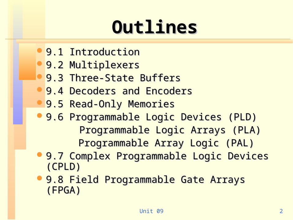
OutlinesOutlines 9.1 Introduction9.1 Introduction 9.2 Multiplexers9.2 Multiplexers 9.3 Three-State Buffers9.3 Three-State Buffers 9.4 Decoders and Encoders9.4 Decoders and Encoders 9.5 Read-Only Memories9.5 Read-Only Memories 9.6 Programmable Logic Devices (PLD)9.6 Programmable Logic Devices (PLD)
Programmable Logic Arrays (PLA)Programmable Logic Arrays (PLA) Programmable Array Logic (PAL)Programmable Array Logic (PAL)
9.7 Complex Programmable Logic Devices 9.7 Complex Programmable Logic Devices (CPLD)(CPLD)
9.8 Field Programmable Gate Arrays (FPGA)9.8 Field Programmable Gate Arrays (FPGA)
Unit 09 3
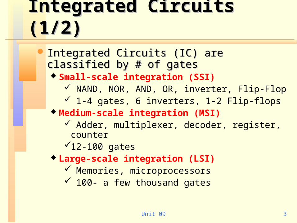
Integrated Circuits (1/2)Integrated Circuits (1/2) Integrated Circuits (IC) are classified by # of Integrated Circuits (IC) are classified by # of
gatesgates Small-scale integration (SSI)
NAND, NOR, AND, OR, inverter, Flip-Flop 1-4 gates, 6 inverters, 1-2 Flip-flops
Medium-scale integration (MSI) Adder, multiplexer, decoder, register, counter12-100 gates
Large-scale integration (LSI) Memories, microprocessors 100- a few thousand gates
Unit 09 4
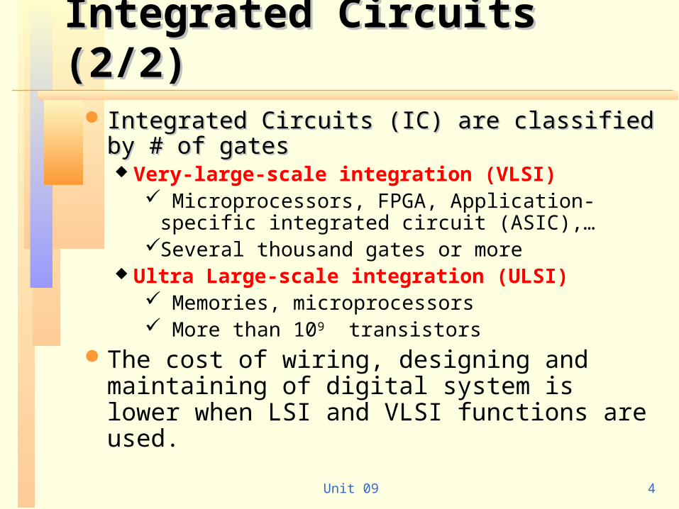
Integrated Circuits (2/2)Integrated Circuits (2/2) Integrated Circuits (IC) are classified by # of Integrated Circuits (IC) are classified by # of
gatesgates Very-large-scale integration (VLSI)
Microprocessors, FPGA, Application-specific integrated circuit (ASIC),…
Several thousand gates or more Ultra Large-scale integration (ULSI)
Memories, microprocessors More than 109 transistors
The cost of wiring, designing and maintaining of digital system is lower when LSI and VLSI functions are used.
Unit 09 5
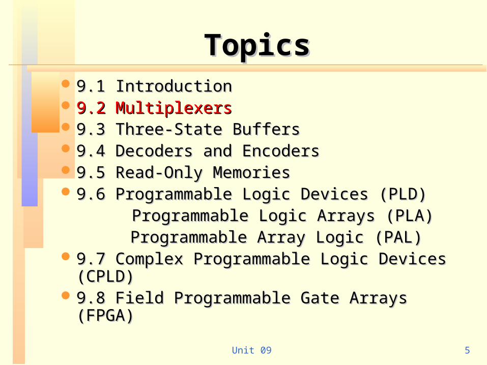
TopicsTopics 9.1 Introduction9.1 Introduction 9.2 Multiplexers9.2 Multiplexers 9.3 Three-State Buffers9.3 Three-State Buffers 9.4 Decoders and Encoders9.4 Decoders and Encoders 9.5 Read-Only Memories9.5 Read-Only Memories 9.6 Programmable Logic Devices (PLD)9.6 Programmable Logic Devices (PLD)
Programmable Logic Arrays (PLA)Programmable Logic Arrays (PLA) Programmable Array Logic (PAL)Programmable Array Logic (PAL)
9.7 Complex Programmable Logic Devices 9.7 Complex Programmable Logic Devices (CPLD)(CPLD)
9.8 Field Programmable Gate Arrays (FPGA)9.8 Field Programmable Gate Arrays (FPGA)
Unit 09 6
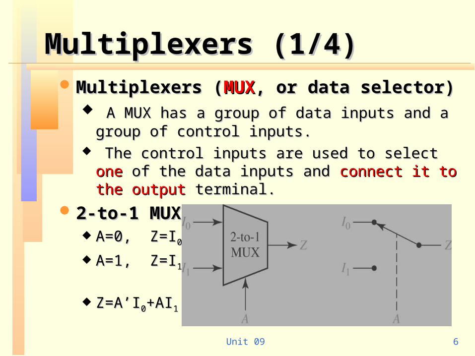
Multiplexers (1/4)Multiplexers (1/4) Multiplexers (Multiplexers (MUXMUX, or data selector), or data selector)
A MUX has a group of data inputs and a group of A MUX has a group of data inputs and a group of control inputs.control inputs.
The control inputs are used to select The control inputs are used to select oneone of the of the data inputs and data inputs and connect it to the outputconnect it to the output terminal. terminal.
2-to-1 MUX2-to-1 MUX A=0, Z=IA=0, Z=I00
A=1, Z=IA=1, Z=I11
Z=A’IZ=A’I00+AI+AI11
Unit 09 7
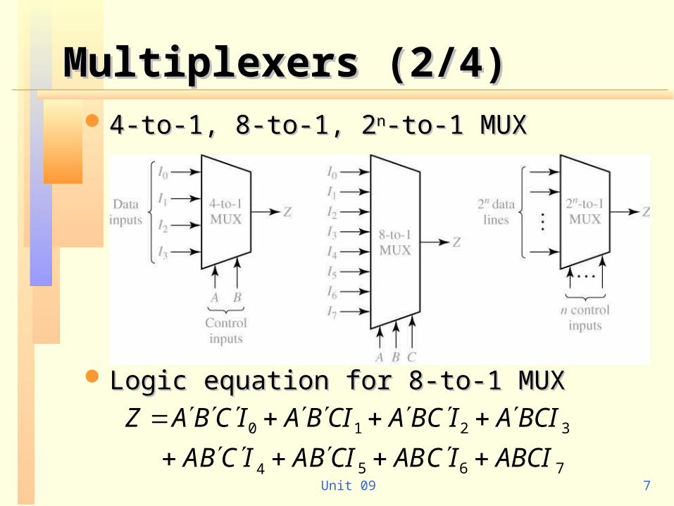
Multiplexers (2/4)Multiplexers (2/4) 4-to-1, 8-to-1, 24-to-1, 8-to-1, 2nn-to-1 MUX-to-1 MUX
Logic equation for 8-to-1 MUXLogic equation for 8-to-1 MUX
7654
3210
ABCIICABCIBAICBA
BCIAICBACIBAICBAZ
Unit 09 8
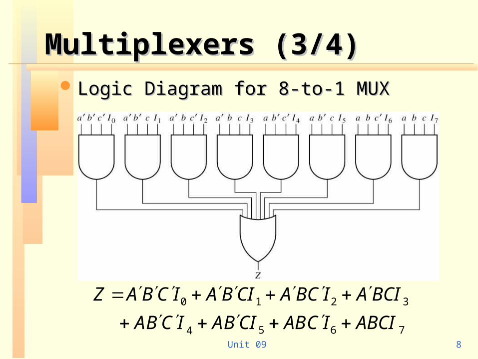
Multiplexers (3/4)Multiplexers (3/4) Logic Diagram for 8-to-1 MUXLogic Diagram for 8-to-1 MUX
7654
3210
ABCIICABCIBAICBA
BCIAICBACIBAICBAZ
Unit 09 9
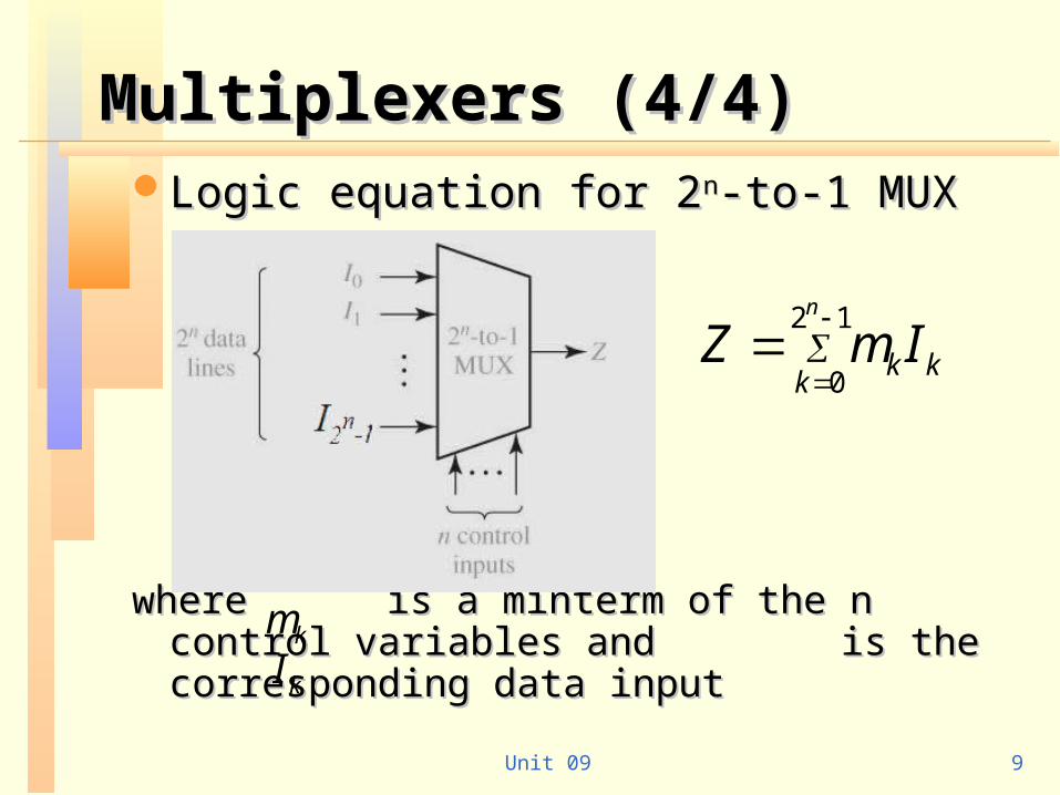
Multiplexers (4/4)Multiplexers (4/4)Logic equation for 2Logic equation for 2nn-to-1 MUX-to-1 MUX
where is a minterm of the n control variables where is a minterm of the n control variables
and is the corresponding data input and is the corresponding data input
12
0
n
kkk ImZ
km
kI
Unit 09 10
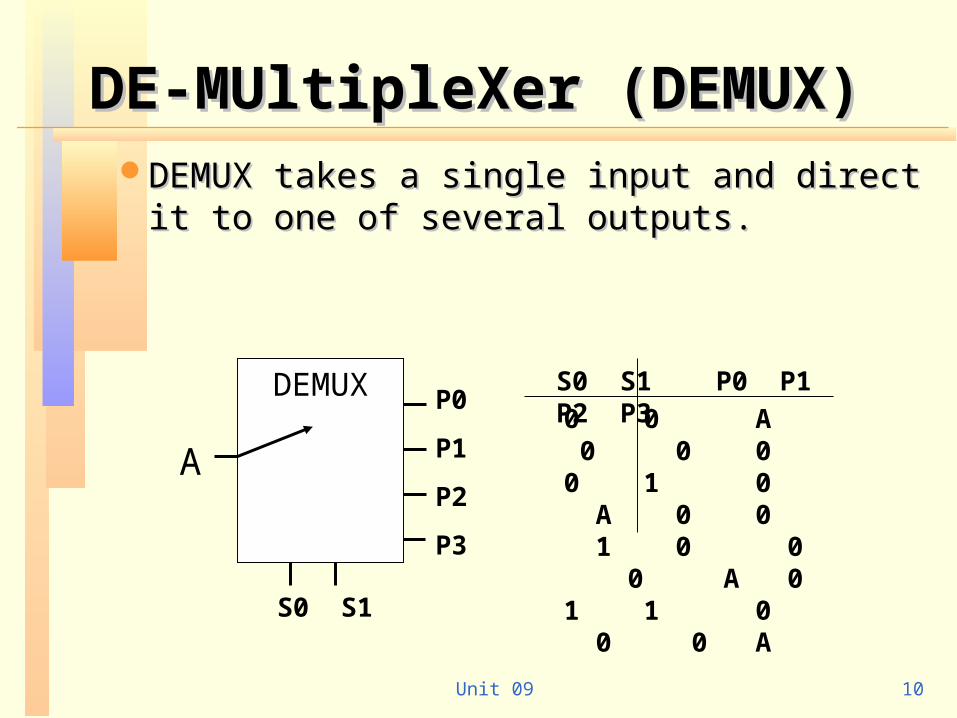
DE-MUltipleXer (DEMUX)DE-MUltipleXer (DEMUX)DEMUX takes a single input and direct it DEMUX takes a single input and direct it
to one of several outputs.to one of several outputs.
DEMUX
A
P0
P1
P2
P3
S0 S1
S0 S1 P0 P1 P2 P3
0 0 A 0 0 0 0 1 0 A 0 0 1 0 0 0 A 0 1 1 0 0 0 A
Unit 09 11
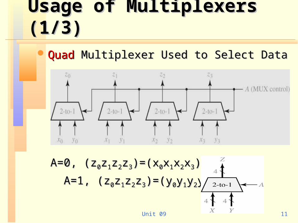
Usage of Multiplexers (1/3)Usage of Multiplexers (1/3) QuadQuad Multiplexer Used to Select Data Multiplexer Used to Select Data
A=0, (zA=0, (z00zz11zz22zz33)=(x)=(x00xx11xx22xx33))
A=1, (zA=1, (z00zz11zz22zz33)=(y)=(y00yy11yy22yy33))
Unit 09 12
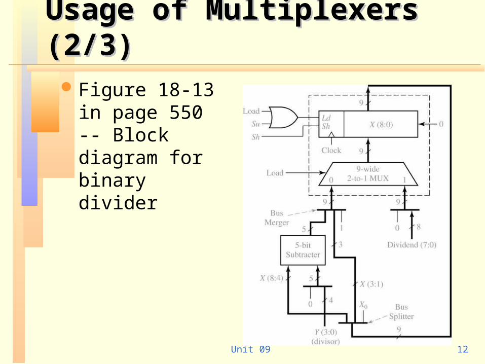
Usage of Multiplexers (2/3)Usage of Multiplexers (2/3)Figure 18-13 in
page 550 -- Block diagram for binary divider
Unit 09 13
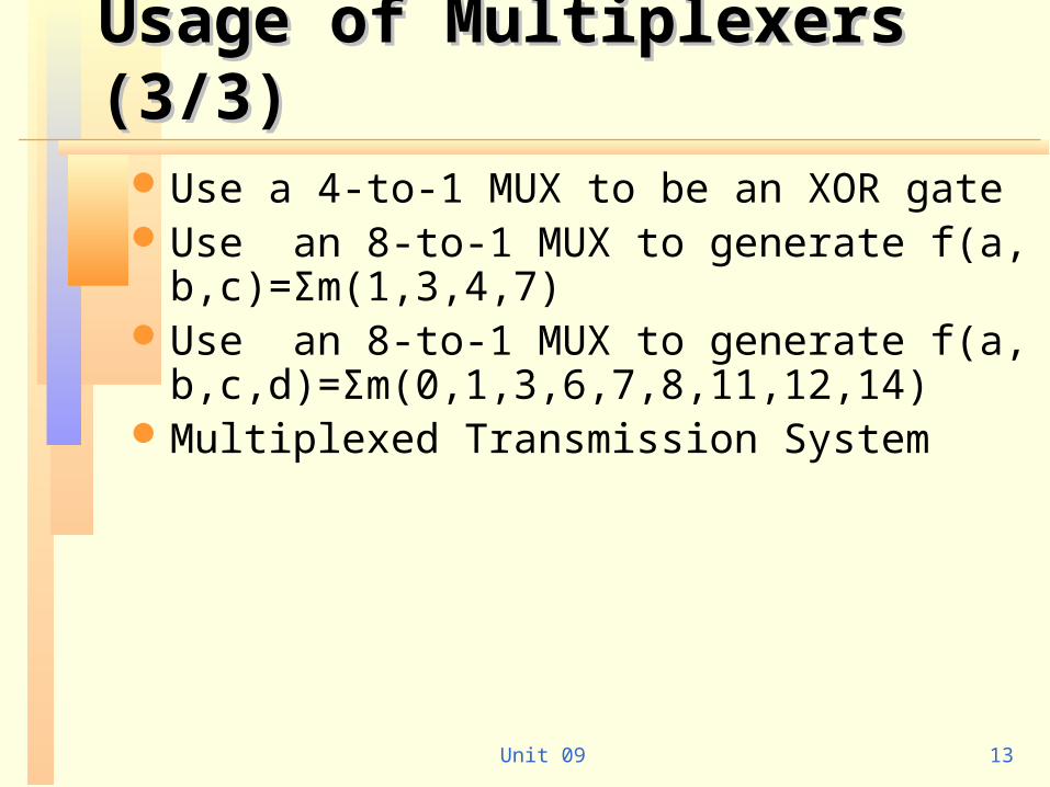
Usage of Multiplexers (3/3)Usage of Multiplexers (3/3)Use a 4-to-1 MUX to be an XOR gateUse an 8-to-1 MUX to generate f(a,b,c)=Σm(1,
3,4,7)Use an 8-to-1 MUX to generate f(a,b,c,d)=Σm
(0,1,3,6,7,8,11,12,14)Multiplexed Transmission System
Unit 09 14
TopicsTopics 9.1 Introduction9.1 Introduction 9.2 Multiplexers9.2 Multiplexers 9.3 9.3 Three-State BuffersThree-State Buffers 9.4 Decoders and Encoders9.4 Decoders and Encoders 9.5 Read-Only Memories9.5 Read-Only Memories 9.6 Programmable Logic Devices (PLD)9.6 Programmable Logic Devices (PLD)
Programmable Logic Arrays (PLA)Programmable Logic Arrays (PLA) Programmable Array Logic (PAL)Programmable Array Logic (PAL)
9.7 Complex Programmable Logic Devices 9.7 Complex Programmable Logic Devices (CPLD)(CPLD)
9.8 Field Programmable Gate Arrays (FPGA)9.8 Field Programmable Gate Arrays (FPGA)
Unit 09 15
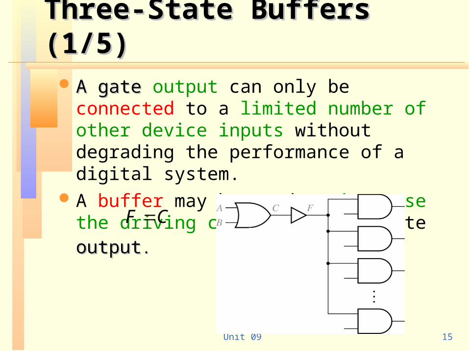
Three-State Buffers (1/5)Three-State Buffers (1/5) A gate A gate output can only be connected to a
limited number of other device inputs without degrading the performance of a digital system.
A buffer may be used to increase the driving capability of a gate output output..
CF
Unit 09 16
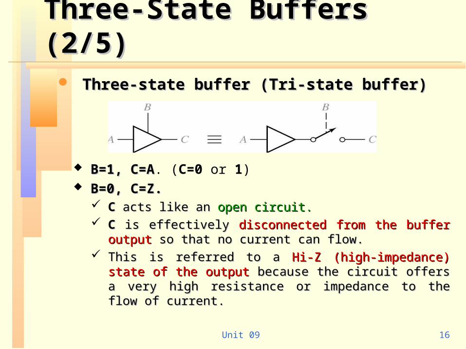
Three-State Buffers (2/5)Three-State Buffers (2/5) Three-state buffer (Tri-state buffer)Three-state buffer (Tri-state buffer)
B=1, C=AB=1, C=A. (C=0 or 1) B=0, C=Z. B=0, C=Z.
C C acts like anacts like an open circuit. open circuit. C C is effectivelyis effectively disconnected from the buffer outputdisconnected from the buffer output so so
that no current can flow. that no current can flow. This is referred to a This is referred to a Hi-Z (high-impedance) state of the Hi-Z (high-impedance) state of the
outputoutput because the circuit offers a very high resistance because the circuit offers a very high resistance or impedance to the flow of current.or impedance to the flow of current.
Unit 09 17
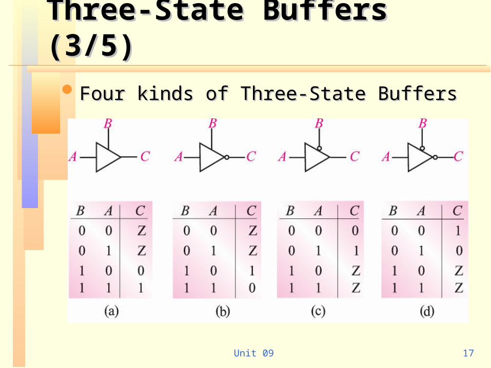
Three-State Buffers (3/5)Three-State Buffers (3/5) Four kinds of Three-State BuffersFour kinds of Three-State Buffers
Unit 09 18
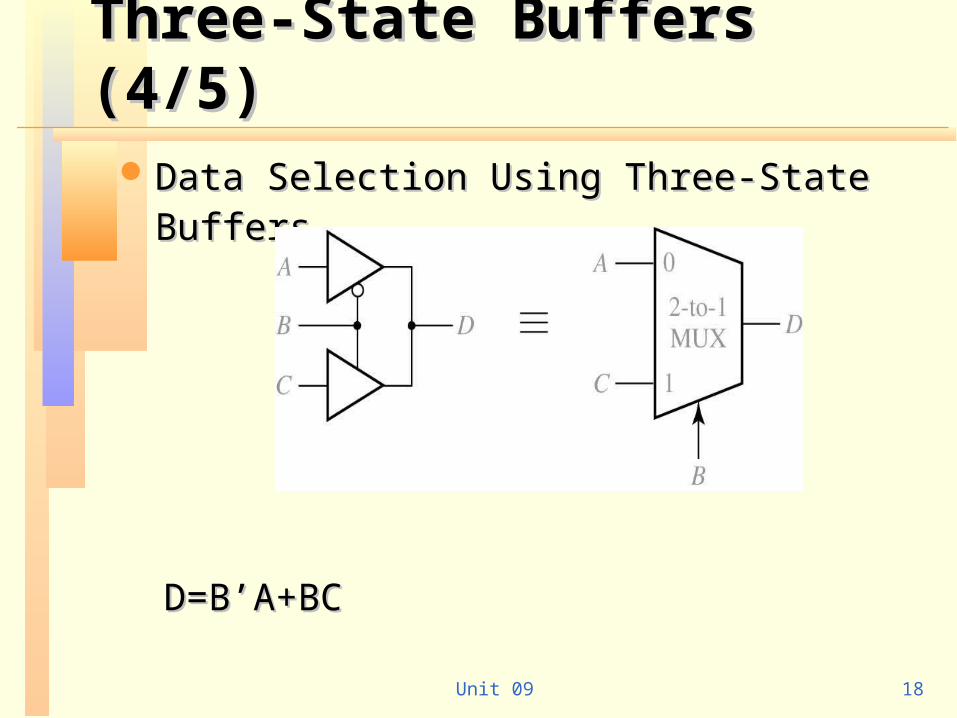
Three-State Buffers (4/5)Three-State Buffers (4/5) Data Selection Using Three-State BuffersData Selection Using Three-State Buffers
D=B’A+BCD=B’A+BC
Unit 09 19
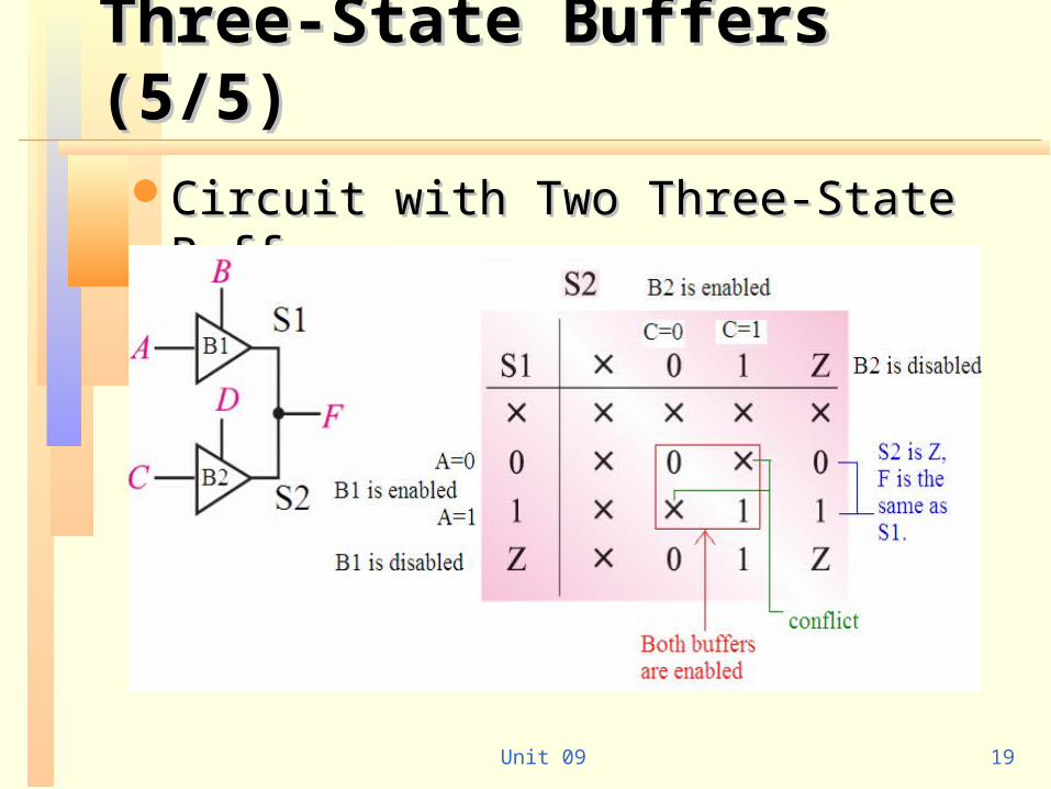
Three-State Buffers (5/5)Three-State Buffers (5/5)Circuit with Two Three-State BuffersCircuit with Two Three-State Buffers
Unit 09 20
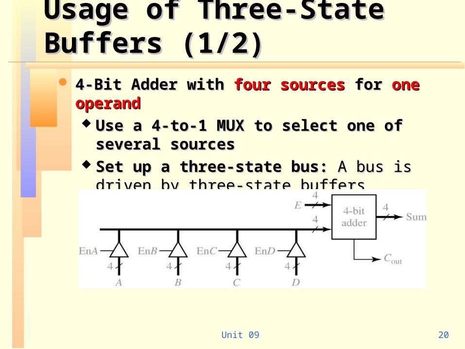
Usage of Three-State Buffers Usage of Three-State Buffers (1/2)(1/2)
4-Bit Adder with 4-Bit Adder with four sourcesfour sources for for one operandone operand Use a 4-to-1 MUX to select one of several Use a 4-to-1 MUX to select one of several
sourcessources Set up a three-state bus: Set up a three-state bus: A bus is driven by A bus is driven by
three-state buffersthree-state buffers
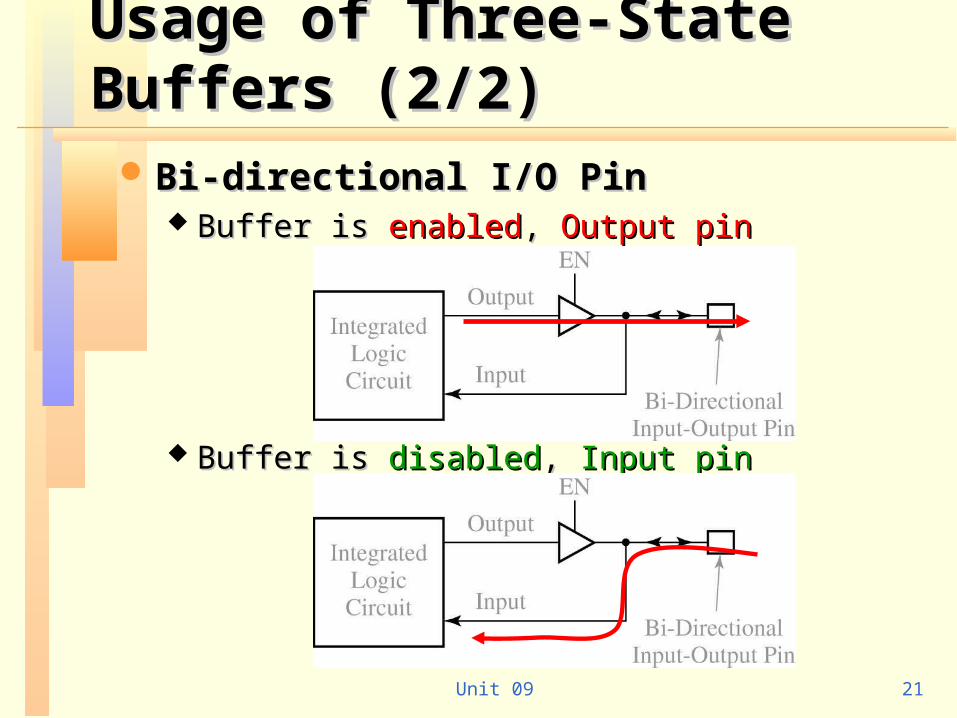
Unit 09 21
Usage of Three-State Buffers Usage of Three-State Buffers (2/2)(2/2)
Bi-directional I/O PinBi-directional I/O Pin Buffer is Buffer is enabledenabled, , Output pinOutput pin
Buffer is Buffer is disableddisabled, , Input pinInput pin
Unit 09 22
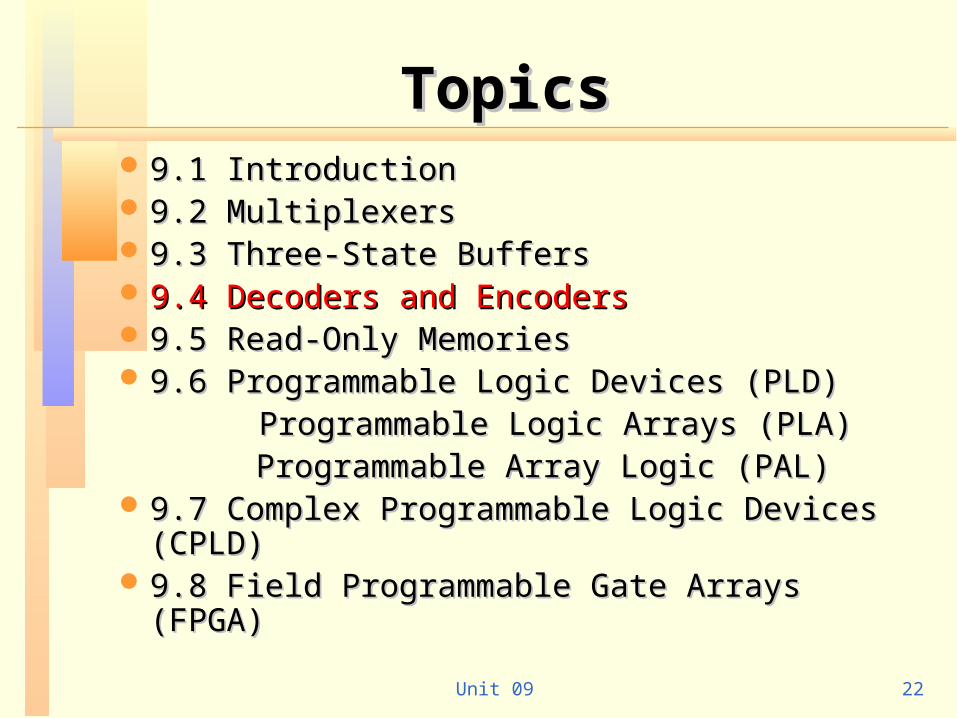
TopicsTopics 9.1 Introduction9.1 Introduction 9.2 Multiplexers9.2 Multiplexers 9.3 Three-State Buffers9.3 Three-State Buffers 9.4 Decoders and Encoders9.4 Decoders and Encoders 9.5 Read-Only Memories9.5 Read-Only Memories 9.6 Programmable Logic Devices (PLD)9.6 Programmable Logic Devices (PLD)
Programmable Logic Arrays (PLA)Programmable Logic Arrays (PLA) Programmable Array Logic (PAL)Programmable Array Logic (PAL)
9.7 Complex Programmable Logic Devices 9.7 Complex Programmable Logic Devices (CPLD)(CPLD)
9.8 Field Programmable Gate Arrays (FPGA)9.8 Field Programmable Gate Arrays (FPGA)
Unit 09 23
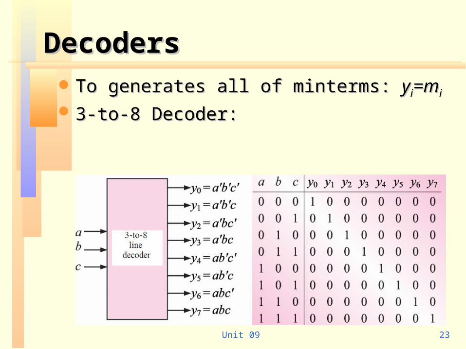
DecodersDecoders To generates all of minterms: To generates all of minterms: yyii=m=mii
3-to-8 Decoder: 3-to-8 Decoder:
Unit 09 24
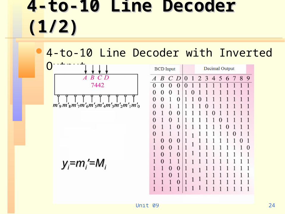
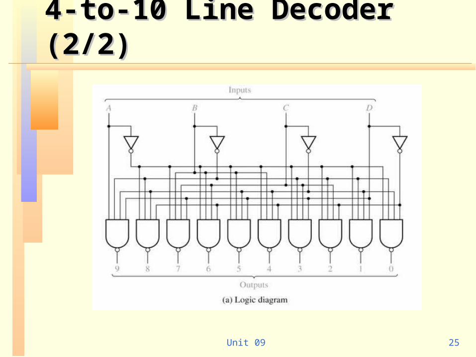
4-to-10 Line Decoder (1/2)4-to-10 Line Decoder (1/2)4-to-10 Line Decoder with Inverted Output
yyii=m=mii’=M’=Mi i
Unit 09 25
4-to-10 Line Decoder (2/2)4-to-10 Line Decoder (2/2)
Unit 09 26
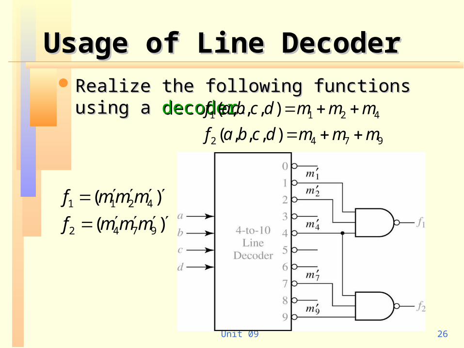
Usage of Line DecoderUsage of Line Decoder Realize the following functions using a Realize the following functions using a
decoderdecoder..
)(
)(
9742
4211
mmmf
mmmf
9742
4211
),,,(
),,,(
mmmdcbaf
mmmdcbaf
Unit 09 27
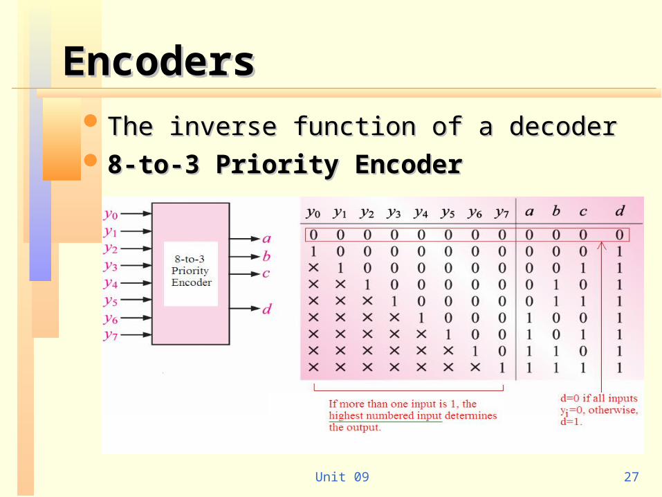
EncodersEncoders The inverse function of a decoderThe inverse function of a decoder 8-to-3 Priority Encoder8-to-3 Priority Encoder
Unit 09 28
TopicsTopics 9.1 Introduction9.1 Introduction 9.2 Multiplexers9.2 Multiplexers 9.3 Three-State Buffers9.3 Three-State Buffers 9.4 Decoders and Encoders9.4 Decoders and Encoders 9.5 Read-Only Memories9.5 Read-Only Memories 9.6 Programmable Logic Devices (PLD)9.6 Programmable Logic Devices (PLD)
Programmable Logic Arrays (PLA)Programmable Logic Arrays (PLA) Programmable Array Logic (PAL)Programmable Array Logic (PAL)
9.7 Complex Programmable Logic Devices 9.7 Complex Programmable Logic Devices (CPLD)(CPLD)
9.8 Field Programmable Gate Arrays (FPGA)9.8 Field Programmable Gate Arrays (FPGA)
Unit 09 29
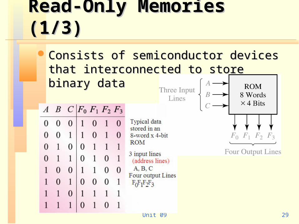
Read-Only Memories (1/3)Read-Only Memories (1/3) Consists of semiconductor devices that Consists of semiconductor devices that
interconnected to store binary data interconnected to store binary data
Unit 09 30
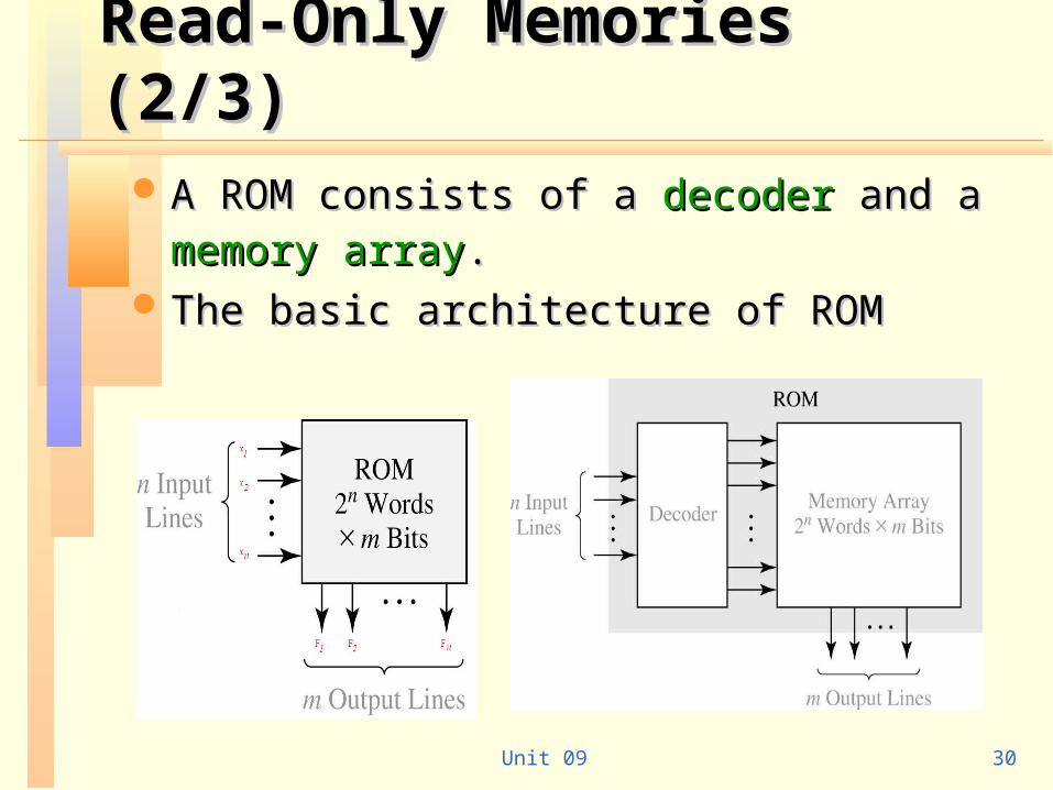
Read-Only Memories (2/3)Read-Only Memories (2/3) A ROM consists of aA ROM consists of a decoder decoder and a and a memory memory
arrayarray.. The basic architecture of ROMThe basic architecture of ROM
Unit 09 31
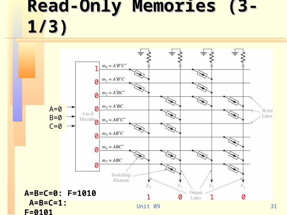
Read-Only Memories (3-1/3)Read-Only Memories (3-1/3)
A=B=C=0: F=1010 A=B=C=1: F=0101
A=0 B=0 C=0
0
1
0
0
0
0
0
0
0 011
Unit 09 32
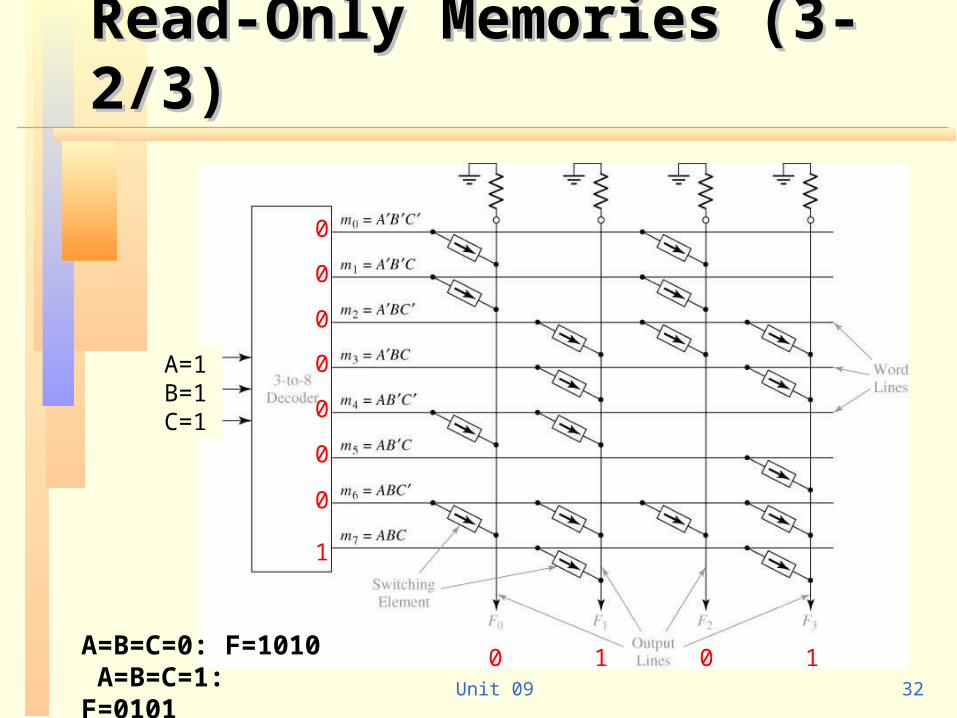
Read-Only Memories (3-2/3)Read-Only Memories (3-2/3)
A=B=C=0: F=1010 A=B=C=1: F=0101
A=1 B=1 C=1
0
0
0
0
0
0
0
1
1 100
Unit 09 33
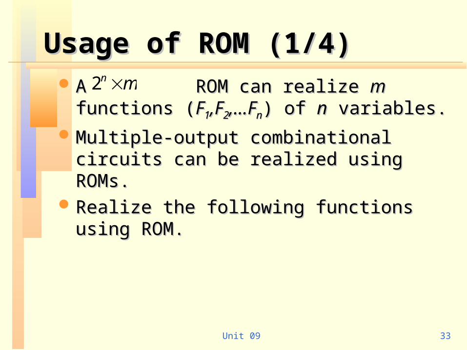
Usage of ROM (1/4)Usage of ROM (1/4) A ROM can realize A ROM can realize mm functions ( functions (FF11,F,F22,…,…
FFnn) of ) of nn variables. variables.
Multiple-output combinational circuits can be Multiple-output combinational circuits can be realized using ROMs.realized using ROMs.
Realize the following functions using ROM.Realize the following functions using ROM.
mn 2
Unit 09 34
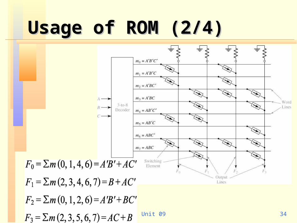
Usage of ROM (2/4)Usage of ROM (2/4)
Unit 09 35
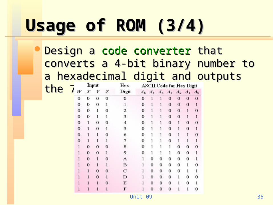
Usage of ROM (3/4)Usage of ROM (3/4) Design a Design a code convertercode converter that converts a 4-bit that converts a 4-bit
binary number to a hexadecimal digit and binary number to a hexadecimal digit and outputs the 7-bit ASCII code.outputs the 7-bit ASCII code.
Unit 09 36
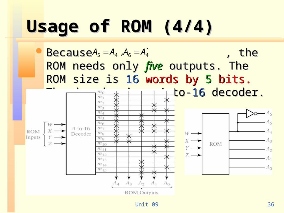
Usage of ROM (4/4)Usage of ROM (4/4) Because , the ROM needs only Because , the ROM needs only fivefive outputs. The ROM size is outputs. The ROM size is 1616 words by words by 55 bits. bits. The decoder is a 4-to-The decoder is a 4-to-1616 decoder. decoder.
4645 , AAAA
Unit 09 37
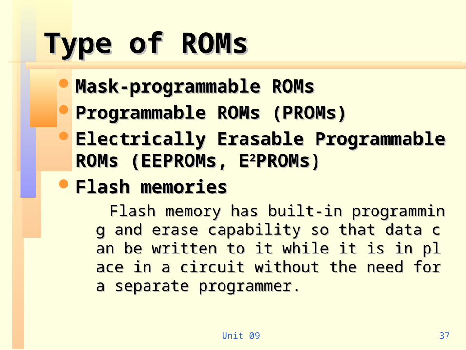
Type of ROMsType of ROMs Mask-programmable ROMsMask-programmable ROMs Programmable ROMs (PROMs)Programmable ROMs (PROMs) Electrically Erasable Programmable ROMs Electrically Erasable Programmable ROMs
(EEPROMs, E(EEPROMs, E22PROMs)PROMs) Flash memoriesFlash memories
Flash memory has built-in programming and erase Flash memory has built-in programming and erase capability so that data can be written to it while it is capability so that data can be written to it while it is in place in a circuit without the need for a separate in place in a circuit without the need for a separate programmer.programmer.
Unit 09 38
TopicsTopics 9.1 Introduction9.1 Introduction 9.2 Multiplexers9.2 Multiplexers 9.3 Three-State Buffers9.3 Three-State Buffers 9.4 Decoders and Encoders9.4 Decoders and Encoders 9.5 Read-Only Memories9.5 Read-Only Memories 9.6 Programmable Logic Devices (PLD)9.6 Programmable Logic Devices (PLD)
Programmable Logic Arrays (PLA)Programmable Logic Arrays (PLA) Programmable Array Logic (PAL)Programmable Array Logic (PAL)
9.7 Complex Programmable Logic Devices 9.7 Complex Programmable Logic Devices (CPLD)(CPLD)
9.8 Field Programmable Gate Arrays (FPGA)9.8 Field Programmable Gate Arrays (FPGA)
Unit 09 39
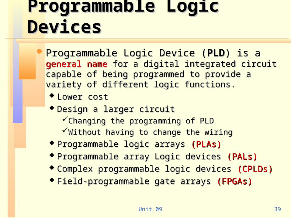
Programmable Logic DevicesProgrammable Logic Devices Programmable Logic Device (Programmable Logic Device (PLDPLD) is a ) is a general general
namename for a digital integrated circuit capable of being for a digital integrated circuit capable of being programmed to provide a variety of different logic programmed to provide a variety of different logic functions.functions. Lower costLower cost Design a larger circuitDesign a larger circuit
Changing the programming of PLDChanging the programming of PLDWithout having to change the wiringWithout having to change the wiring
Programmable logic arraysProgrammable logic arrays (PLAs) (PLAs) Programmable array Logic devicesProgrammable array Logic devices (PALs) (PALs) Complex programmable logic devicesComplex programmable logic devices (CPLDs) (CPLDs) Field-programmable gate arraysField-programmable gate arrays (FPGAs) (FPGAs)
Unit 09 40
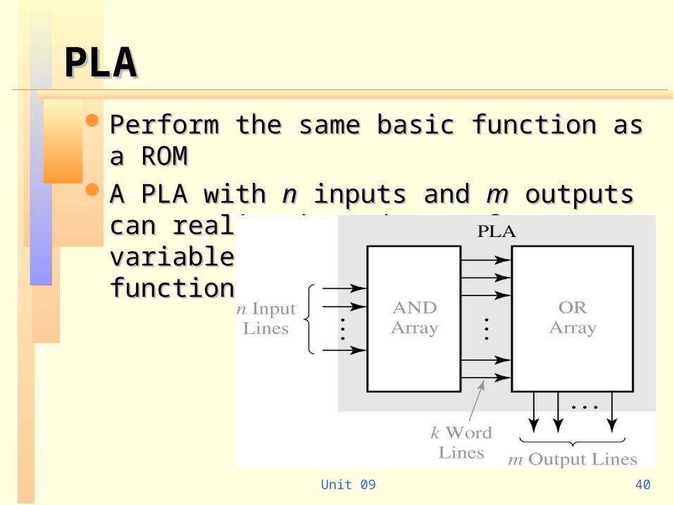
PLAPLA Perform the same basic function as a ROMPerform the same basic function as a ROM A PLA with A PLA with nn inputs and inputs and mm outputs can realize outputs can realize
kk products of products of nn variables then generate variables then generate mm functions .functions .
Unit 09 41
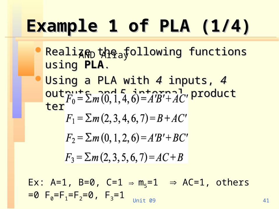
Example 1 of PLA (1/4)Example 1 of PLA (1/4) Realize the following functions using Realize the following functions using PLAPLA.. Using a PLA with Using a PLA with 44 inputs, inputs, 44 outputs and outputs and 5 5
internal product terms.internal product terms.
Ex: A=1, B=0, C=1 m5=1 AC=1, others =0 F0=F1=F2=0, F3=1
AND Array
Unit 09 42
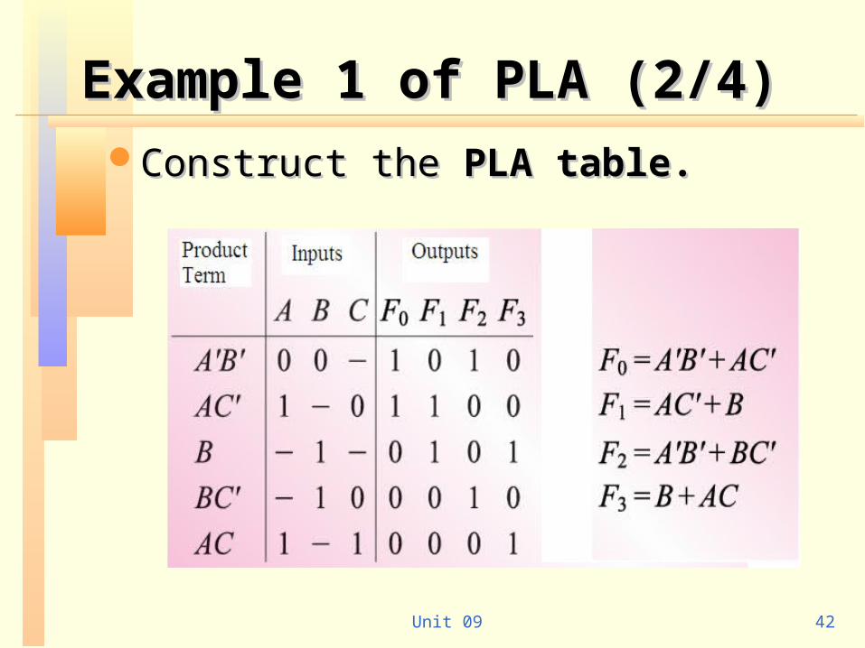
Example 1 of PLA (2/4)Example 1 of PLA (2/4)Construct the Construct the PLAPLA table.table.
Unit 09 43
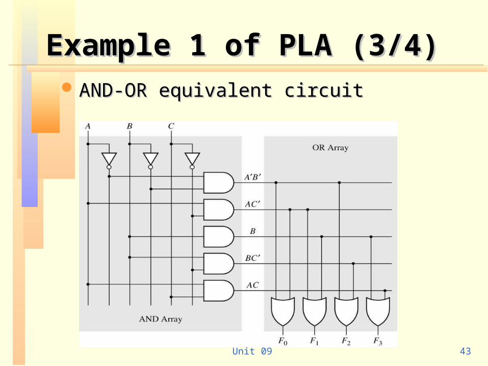
Example 1 of PLA (3/4) Example 1 of PLA (3/4) AND-ORAND-OR equivalent circuitequivalent circuit
Unit 09 44
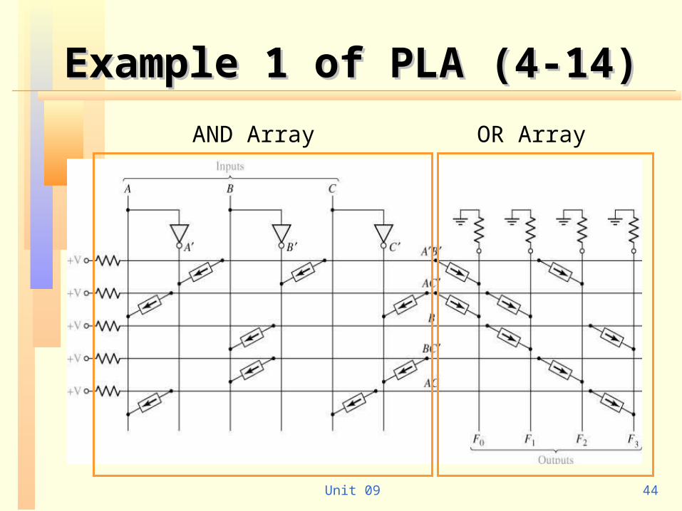
Example 1 of PLA (4-14)Example 1 of PLA (4-14)
AND Array OR Array
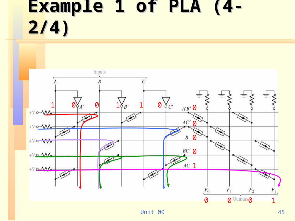
Unit 09 45
Example 1 of PLA (4-2/4)Example 1 of PLA (4-2/4)
01 0 1 1 0 0
0
0
0
1
0 00 1
Unit 09 46
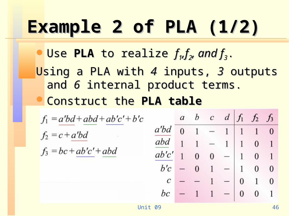
Example 2 of PLA (1/2)Example 2 of PLA (1/2) Use Use PLAPLA to realize to realize ff11,f,f22, and f, and f33..
Using a PLA with Using a PLA with 44 inputs, inputs, 33 outputs and outputs and 66 internal product terms.internal product terms.
Construct the Construct the PLAPLA tabletable
Unit 09 47
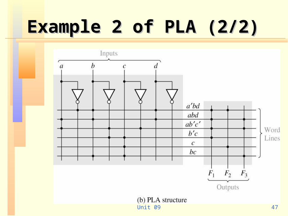
Example 2 of PLA (2/2)Example 2 of PLA (2/2)
Unit 09 48
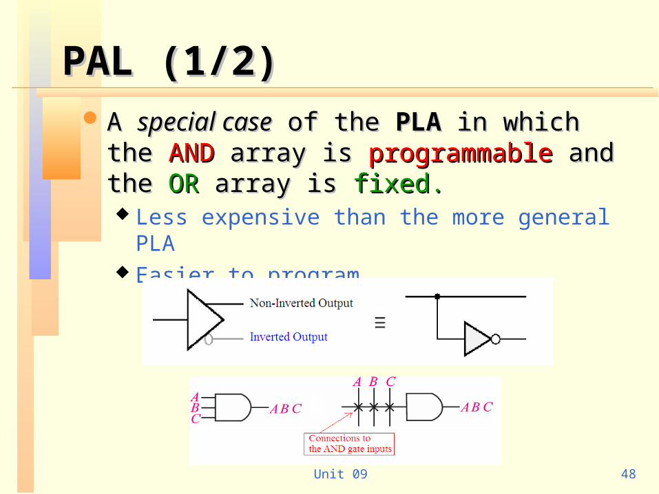
PAL (1/2)PAL (1/2) A A special casespecial case of the of the PLAPLA in which the in which the ANDAND
array is array is programmableprogrammable and the and the OROR array is array is fixed.fixed. Less expensive than the more general PLA Easier to program
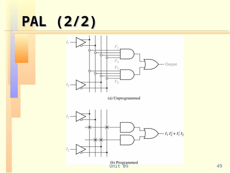
Unit 09 49
PAL (2/2)PAL (2/2)
Unit 09 50
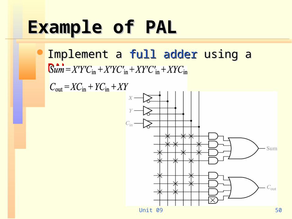
Example of PALExample of PAL Implement a Implement a full adderfull adder using a using a PALPAL..
Unit 09 51
TopicsTopics 9.1 Introduction9.1 Introduction 9.2 Multiplexers9.2 Multiplexers 9.3 Three-State Buffers9.3 Three-State Buffers 9.4 Decoders and Encoders9.4 Decoders and Encoders 9.5 Read-Only Memories9.5 Read-Only Memories 9.6 Programmable Logic Devices (PLD)9.6 Programmable Logic Devices (PLD)
Programmable Logic Arrays (PLA)Programmable Logic Arrays (PLA) Programmable Array Logic (PAL)Programmable Array Logic (PAL)
9.7 Complex Programmable Logic Devices 9.7 Complex Programmable Logic Devices (CPLD)(CPLD)
9.8 Field Programmable Gate Arrays (FPGA)9.8 Field Programmable Gate Arrays (FPGA)
Unit 09 52
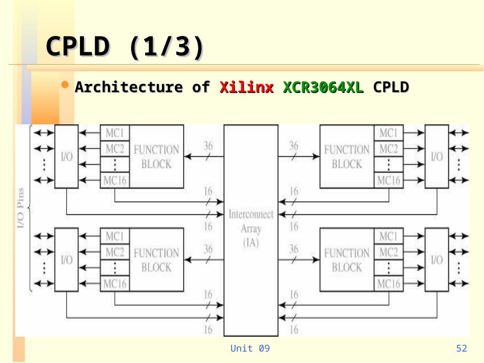
CPLD (1/3)CPLD (1/3) Architecture of Architecture of Xilinx Xilinx XCR3064XL XCR3064XL CPLDCPLD
Unit 09 53
CPLD (2/3)CPLD (2/3) 4 function blocks (FBs)4 function blocks (FBs)
Each Each FBFB has has 1616 associated associated macrocellsmacrocells (MC1, MC (MC1, MC2,…).2,…).• Each macrocell contains a Each macrocell contains a flip-flopflip-flop and and multiplexersmultiplexers that that rr
outeoute signals from the signals from the FBFB to the to the I/O blockI/O block or to the or to the intercointerconnect array (IA)nnect array (IA)
Each Each FBFB is a is a programmable AND-OR arrayprogrammable AND-OR array that is co that is configured as a PLA.nfigured as a PLA.
The The IAIA selects signals from the selects signals from the macrocellmacrocell outputs or outputs or I/I/OO blocksblocks and connects them back to and connects them back to FBFB inputs. inputs.
A signal generated in one A signal generated in one FBFB can be used as an can be used as an inputinput to to any other any other FBFB..
The The I/O blocksI/O blocks provide an interface between the provide an interface between the bi-dirbi-directional I/O pinsectional I/O pins on the IC and the on the IC and the interior interior of the CPLD. of the CPLD.
Unit 09 54
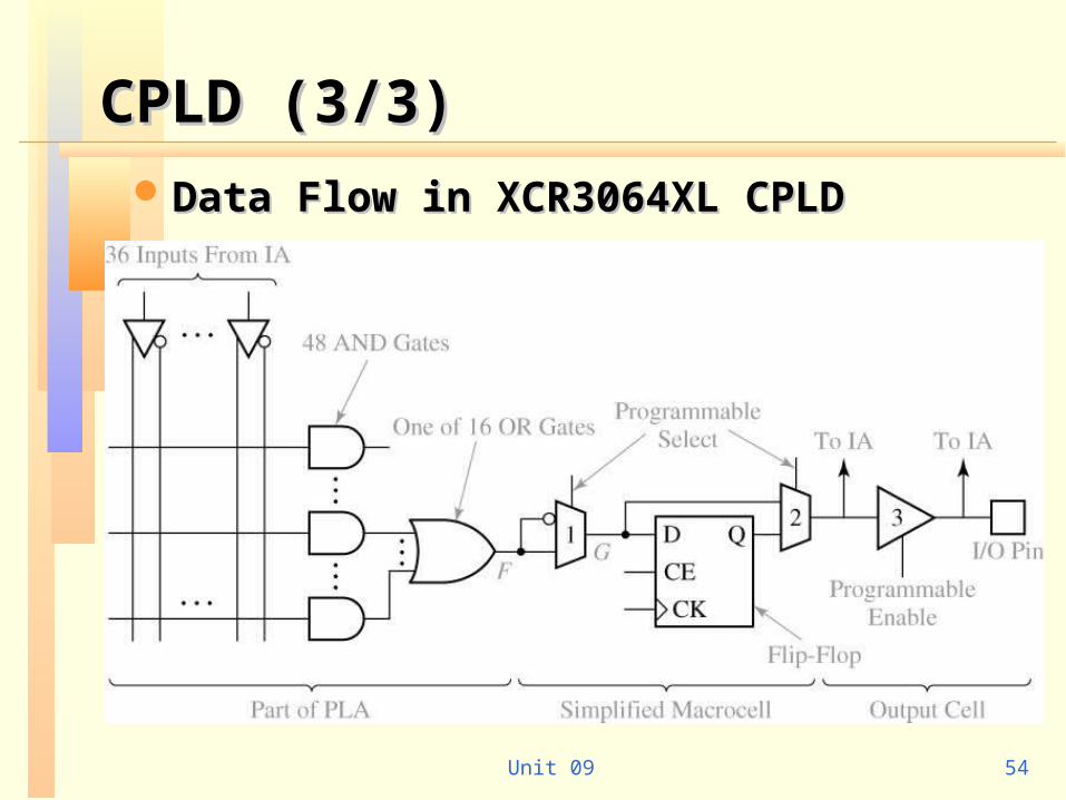
CPLD (3/3)CPLD (3/3) Data Flow in XCR3064XL CPLD Data Flow in XCR3064XL CPLD
Unit 09 55
TopicsTopics 9.1 Introduction9.1 Introduction 9.2 Multiplexers9.2 Multiplexers 9.3 Three-State Buffers9.3 Three-State Buffers 9.4 Decoders and Encoders9.4 Decoders and Encoders 9.5 Read-Only Memories9.5 Read-Only Memories 9.6 Programmable Logic Devices (PLD)9.6 Programmable Logic Devices (PLD)
Programmable Logic Arrays (PLA)Programmable Logic Arrays (PLA) Programmable Array Logic (PAL)Programmable Array Logic (PAL)
9.7 Complex Programmable Logic Devices 9.7 Complex Programmable Logic Devices (CPLD)(CPLD)
9.8 Field Programmable Gate Arrays (FPGA)9.8 Field Programmable Gate Arrays (FPGA)
Unit 09 56
FPGAFPGA An FPGA is an IC that contains An FPGA is an IC that contains an array of identican array of identic
al logic cellsal logic cells with with programmable interconnectionsprogrammable interconnections.. The interior of the FPGA consists of an array of logic cThe interior of the FPGA consists of an array of logic c
ells, called configurable logic blocks (CLBs).ells, called configurable logic blocks (CLBs). The array of CLBs is surrounded by a ring of input-outThe array of CLBs is surrounded by a ring of input-out
put interface blocks (I/O blocks).put interface blocks (I/O blocks). The I/O blocks connect the CLB signals to IC pins.The I/O blocks connect the CLB signals to IC pins. The space between the CLBs is used to route connectiThe space between the CLBs is used to route connecti
ons between the CLB outputs and inputs.ons between the CLB outputs and inputs.
The user can program the functions realized by eThe user can program the functions realized by each CLB and connections between CLBs.ach CLB and connections between CLBs.
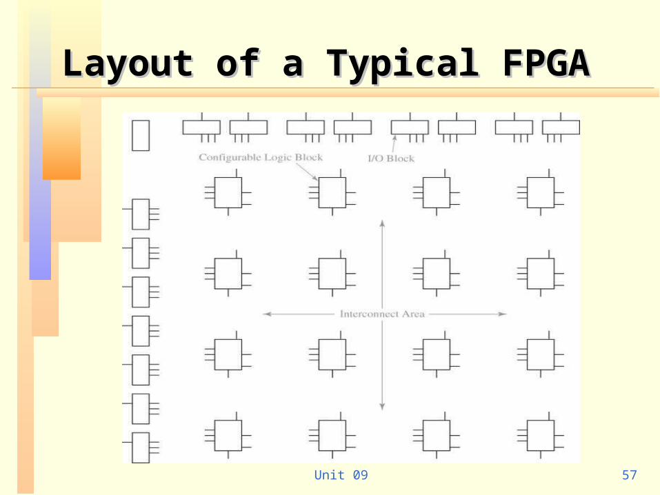
Unit 09 57
Layout of a Typical FPGALayout of a Typical FPGA
Unit 09 58
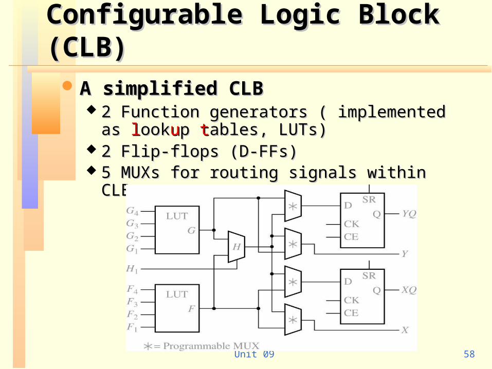
Configurable Logic Block (CLB)Configurable Logic Block (CLB) A simplified CLBA simplified CLB
2 Function generators ( implemented as 2 Function generators ( implemented as llookookuup p ttables, LUTs)ables, LUTs)
2 Flip-flops (D-FFs)2 Flip-flops (D-FFs) 5 MUXs for routing signals within CLB.5 MUXs for routing signals within CLB.
Unit 09 59
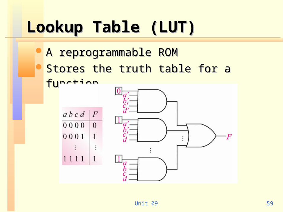
Lookup Table (LUT)Lookup Table (LUT) A reprogrammable ROMA reprogrammable ROM Stores the truth table for a functionStores the truth table for a function
Unit 09 60
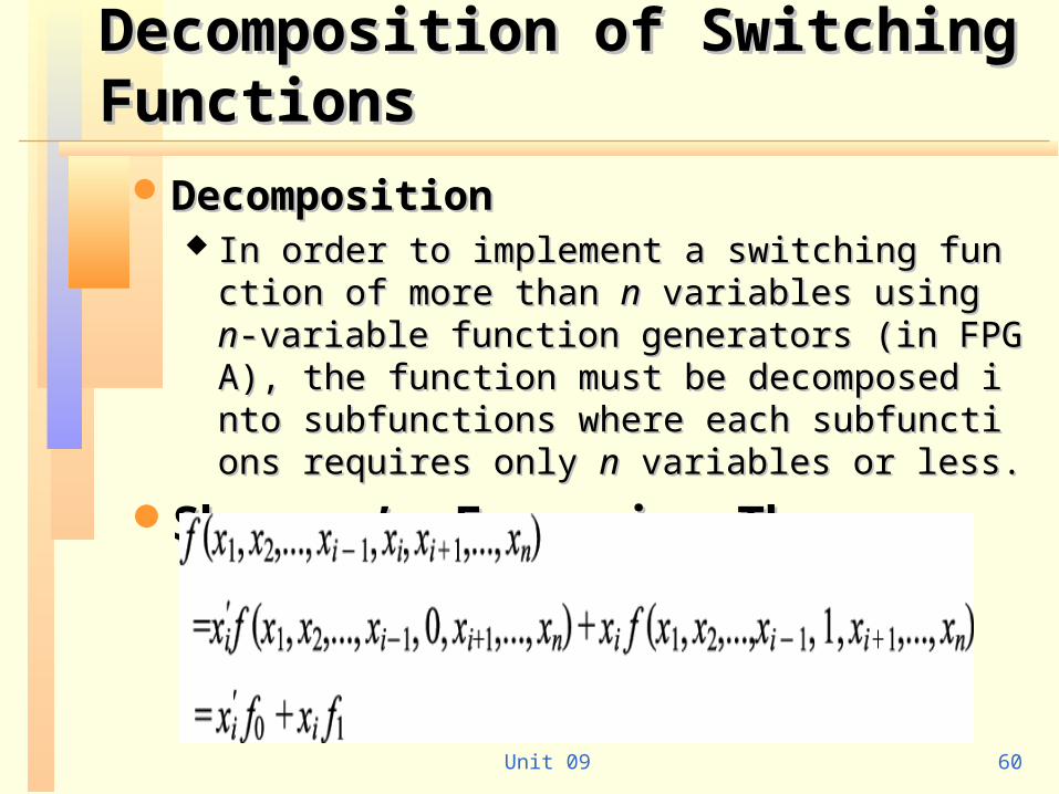
Decomposition of Switching Decomposition of Switching FunctionsFunctions
DecompositionDecomposition In order to implement a switching function of more tIn order to implement a switching function of more t
han han nn variables using variables using nn-variable function generator-variable function generators (in FPGA), the function must be decomposed into s (in FPGA), the function must be decomposed into subfunctions where each subfunctions requires onlsubfunctions where each subfunctions requires only y nn variables or less. variables or less.
Shannon’s Expansion TheoremShannon’s Expansion Theorem
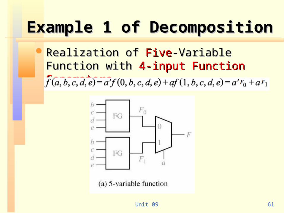
Unit 09 61
Example 1 of DecompositionExample 1 of Decomposition Realization of Realization of FiveFive-Variable Function with -Variable Function with 4-4-
input Function Generatorsinput Function Generators
Unit 09 62
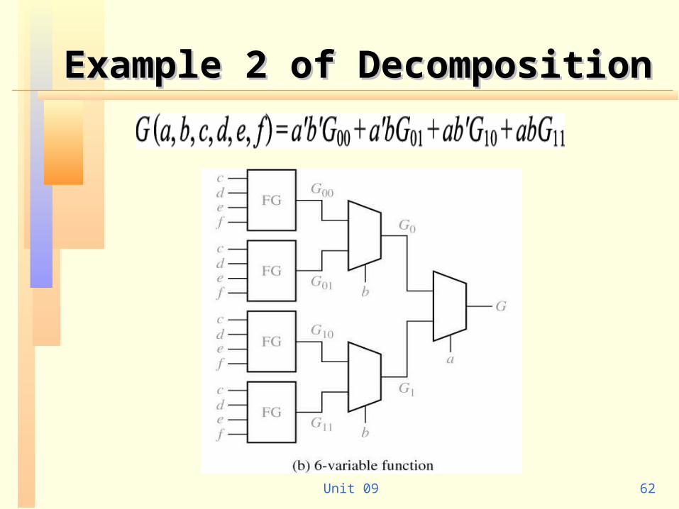
Example 2 of DecompositionExample 2 of Decomposition
Related Documents