Ultrahigh Strength Single Crystalline Nanowhiskers Grown by Physical Vapor Deposition Gunther Richter,* ,† Karla Hillerich, ‡,⊥ Daniel S. Gianola, § Reiner Mo ¨ nig, § Oliver Kraft, § and Cynthia A. Volkert | Max-Planck-Institut fu ¨r Metallforschung, Heisenbergstrasse 3, D-70589 Stuttgart, Germany, Institut fu ¨r Metallkunde, UniVersita ¨t Stuttgart, Heisenbergstrasse 3, D-70589 Stuttgart, Germany, Institut fu ¨r Materialforschung II, Forschungszentrum Karlsruhe, Hermann-Von-Helmholtz-Platz 1, D-76344 Eggenstein-Leopoldshafen, Germany, and Institut fu ¨r Materialphysik, Georg-August UniVersita ¨t Go ¨ttingen, Friedrich-Hund-Platz 1, D-37077 Go ¨ttingen Received May 12, 2009; Revised Manuscript Received July 8, 2009 ABSTRACT The strength of metal crystals is reduced below the theoretical value by the presence of dislocations or by flaws that allow easy nucleation of dislocations. A straightforward method to minimize the number of defects and flaws and to presumably increase its strength is to increase the crystal quality or to reduce the crystal size. Here, we describe the successful fabrication of high aspect ratio nanowhiskers from a variety of face-centered cubic metals using a high temperature molecular beam epitaxy method. The presence of atomically smooth, faceted surfaces and absence of dislocations is confirmed using transmission electron microscopy investigations. Tensile tests performed in situ in a focused- ion beam scanning electron microscope on Cu nanowhiskers reveal strengths close to the theoretical upper limit and confirm that the properties of nanomaterials can be engineered by controlling defect and flaw densities. Single crystalline metal wires, or metal whiskers, with diameters larger than one micrometer have been routinely fabricated 1 and used for experimentally examining mechan- ical, 2 ferromagnetic, 3 superconductive, 4 and electronic 5 prop- erties. Interest in metal whiskers became intense once it was observed that they could exhibit strengths close to theoretical (ideal) values. 2,6 Whiskers have been grown by the vapor liquid solid method 7 (VLS) or metal halide reduction, 6 the latter of which have demonstrated high strength. 6 This has been attributed to the near-equilibrium nature of the growth process and the resultant absence of defects and flaws in the samples. Extending the fabrication of high quality metal whiskers to submicrometer diameters, as routinely produced for semiconductors, 7-9 is clearly desired but has been largely elusive. However, single crystalline metal nanowires have only occasionally been successfully fabricated. 10 Here we describe the first time to our knowledge the fabrication of metal single crystalline nanowhiskers (NWs) with diameters as small as 20 nm and no defects, as evidenced by their strengths near the theoretical upper limit. Such nanostructures have the potential to serve as model systems for elucidating intrinsic properties in tiny structures, such as quantum effects, and to be used as building blocks in nanotechnological applications where unique functionalities are required. In this study, free-standing, high aspect ratio, single crystalline nanowhiskers of a variety of different materials (copper, gold, silver, aluminum, and silicon) have been successfully grown from partially C-coated, oxidized and nonoxidized Si (100), (110), and (111) substrates under molecular beam epitaxy (MBE) conditions. Both elevated substrate temperatures (on the order of 0.65 T M of the deposited species) and the partial C layer are necessary to achieve nanowhisker growth. In the remainder of this publication we will focus on results from Cu nanowhiskers. Figure 1 shows scanning electron micrographs of two Cu samples with nominal Cu thicknesses of 45 and 200 nm, respectively. In addition to whiskers, which are straight and constant in diameter over their length, Cu islands, platelets, and silicide ridges have formed on the substrate. It was observed that whisker growth strongly depends on the carbon layer. Whiskers could not be found on samples without C layer and also did not grow on samples where the C layer * To whom correspondence should be addressed. E-mail: Richter@ mf.mpg.de. † Max-Planck-Institut fu ¨r Metallforschung. ‡ Universita ¨t Stuttgart. § Forschungszentrum Karlsruhe. | Georg-August Universita ¨t Go ¨ttingen. ⊥ Present Address: Solid State Physics, Lund University, Box 118, S-22100 Lund, Sweden. NANO LETTERS 2009 Vol. 9, No. 8 3048-3052 10.1021/nl9015107 CCC: $40.75 2009 American Chemical Society Published on Web 07/28/2009 Downloaded by UNIV OF PENN on August 21, 2009 Published on July 28, 2009 on http://pubs.acs.org | doi: 10.1021/nl9015107

Welcome message from author
This document is posted to help you gain knowledge. Please leave a comment to let me know what you think about it! Share it to your friends and learn new things together.
Transcript
Ultrahigh Strength Single CrystallineNanowhiskers Grown by Physical VaporDepositionGunther Richter,*,† Karla Hillerich,‡,! Daniel S. Gianola,§ Reiner Monig,§Oliver Kraft,§ and Cynthia A. Volkert|
Max-Planck-Institut fur Metallforschung, Heisenbergstrasse 3,D-70589 Stuttgart, Germany, Institut fur Metallkunde, UniVersitat Stuttgart,Heisenbergstrasse 3, D-70589 Stuttgart, Germany, Institut fur Materialforschung II,Forschungszentrum Karlsruhe, Hermann-Von-Helmholtz-Platz 1,D-76344 Eggenstein-Leopoldshafen, Germany, and Institut fur Materialphysik,Georg-August UniVersitat Gottingen, Friedrich-Hund-Platz 1, D-37077 Gottingen
Received May 12, 2009; Revised Manuscript Received July 8, 2009
ABSTRACT
The strength of metal crystals is reduced below the theoretical value by the presence of dislocations or by flaws that allow easy nucleationof dislocations. A straightforward method to minimize the number of defects and flaws and to presumably increase its strength is to increasethe crystal quality or to reduce the crystal size. Here, we describe the successful fabrication of high aspect ratio nanowhiskers from a varietyof face-centered cubic metals using a high temperature molecular beam epitaxy method. The presence of atomically smooth, faceted surfacesand absence of dislocations is confirmed using transmission electron microscopy investigations. Tensile tests performed in situ in a focused-ion beam scanning electron microscope on Cu nanowhiskers reveal strengths close to the theoretical upper limit and confirm that the propertiesof nanomaterials can be engineered by controlling defect and flaw densities.
Single crystalline metal wires, or metal whiskers, withdiameters larger than one micrometer have been routinelyfabricated1 and used for experimentally examining mechan-ical,2 ferromagnetic,3 superconductive,4 and electronic5 prop-erties. Interest in metal whiskers became intense once it wasobserved that they could exhibit strengths close to theoretical(ideal) values.2,6 Whiskers have been grown by the vaporliquid solid method7 (VLS) or metal halide reduction,6 thelatter of which have demonstrated high strength.6 This hasbeen attributed to the near-equilibrium nature of the growthprocess and the resultant absence of defects and flaws in thesamples. Extending the fabrication of high quality metalwhiskers to submicrometer diameters, as routinely producedfor semiconductors,7-9 is clearly desired but has been largelyelusive. However, single crystalline metal nanowires haveonly occasionally been successfully fabricated.10 Here wedescribe the first time to our knowledge the fabrication ofmetal single crystalline nanowhiskers (NWs) with diameters
as small as 20 nm and no defects, as evidenced by theirstrengths near the theoretical upper limit. Such nanostructureshave the potential to serve as model systems for elucidatingintrinsic properties in tiny structures, such as quantum effects,and to be used as building blocks in nanotechnologicalapplications where unique functionalities are required.
In this study, free-standing, high aspect ratio, singlecrystalline nanowhiskers of a variety of different materials(copper, gold, silver, aluminum, and silicon) have beensuccessfully grown from partially C-coated, oxidized andnonoxidized Si (100), (110), and (111) substrates undermolecular beam epitaxy (MBE) conditions. Both elevatedsubstrate temperatures (on the order of 0.65 TM of thedeposited species) and the partial C layer are necessary toachieve nanowhisker growth. In the remainder of thispublication we will focus on results from Cu nanowhiskers.
Figure 1 shows scanning electron micrographs of two Cusamples with nominal Cu thicknesses of 45 and 200 nm,respectively. In addition to whiskers, which are straight andconstant in diameter over their length, Cu islands, platelets,and silicide ridges have formed on the substrate. It wasobserved that whisker growth strongly depends on the carbonlayer. Whiskers could not be found on samples without Clayer and also did not grow on samples where the C layer
* To whom correspondence should be addressed. E-mail: [email protected].
† Max-Planck-Institut fur Metallforschung.‡ Universitat Stuttgart.§ Forschungszentrum Karlsruhe.| Georg-August Universitat Gottingen.! Present Address: Solid State Physics, Lund University, Box 118,
S-22100 Lund, Sweden.
NANOLETTERS
2009Vol. 9, No. 83048-3052
10.1021/nl9015107 CCC: $40.75 " 2009 American Chemical SocietyPublished on Web 07/28/2009
Dow
nloa
ded
by U
NIV
OF
PEN
N o
n A
ugus
t 21,
200
9Pu
blish
ed o
n Ju
ly 2
8, 2
009
on h
ttp://
pubs
.acs
.org
| do
i: 10
.102
1/nl
9015
107
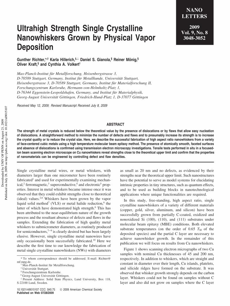
was thicker than 40 nm. Although the effect of differentcarbon layer thicknesses was investigated, no correlationbetween the whisker dimensions and C layer thickness couldbe identified. The carbon mediated whisker growth isconsistent with earlier observations of whisker growth fromseveral decades ago.11 Although a halide process was usedfor the growth, it was found that whisker growth issuppressed on flat and clean substrates. Microscopic observa-tions of the nanowhiskers show that they have a strongtendency to form directly on the oxidized Si wafer atopenings in the C film (Supporting Information, Figure S1).From scanning electron microscopy (SEM) images, it wasfound that the axis of the majority of the whiskers has anangle of less than 30° to the substrate normal. Although thewhiskers show no taper, they grow in length and diameterduring deposition. This was qualitatively confirmed byexperiments where different amounts of Cu were depositedand the dimensions of the resulting whiskers were observedusing SEM. In the particular example of Figure 1a, thewhiskers exhibit a wide distribution of diameters ranging
from 20 to 100 nm and an average length of approximately10 µm, giving aspect ratios as large as 300. Larger nominalCu film thicknesses produce larger whisker lengths anddiameters up to 300 nm in diameter and 75 µm in length(Figure 1b).
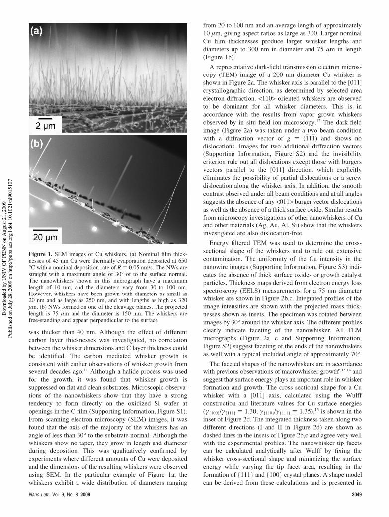
A representative dark-field transmission electron micros-copy (TEM) image of a 200 nm diameter Cu whisker isshown in Figure 2a. The whisker axis is parallel to the [011j]crystallographic direction, as determined by selected areaelectron diffraction. <110> oriented whiskers are observedto be dominant for all whisker diameters. This is inaccordance with the results from vapor grown whiskersobserved by in situ field ion microscopy.12 The dark-fieldimage (Figure 2a) was taken under a two beam conditionwith a diffraction vector of g ) (1j11j) and shows nodislocations. Images for two additional diffraction vectors(Supporting Information, Figure S2) and the invisibilitycriterion rule out all dislocations except those with burgersvectors parallel to the [011] direction, which explicitlyeliminates the possibility of partial dislocations or a screwdislocation along the whisker axis. In addition, the smoothcontrast observed under all beam conditions and at all anglessuggests the absence of any <011> burger vector dislocationsas well as the absence of a thick surface oxide. Similar resultsfrom microscopy investigations of other nanowhiskers of Cuand other materials (Ag, Au, Al, Si) show that the whiskersinvestigated are also dislocation-free.
Energy filtered TEM was used to determine the cross-sectional shape of the whiskers and to rule out extensivecontamination. The uniformity of the Cu intensity in thenanowire images (Supporting Information, Figure S3) indi-cates the absence of thick surface oxides or growth catalystparticles. Thickness maps derived from electron energy lossspectroscopy (EELS) measurements for a 75 nm diameterwhisker are shown in Figure 2b,c. Integrated profiles of theimage intensities are shown with the projected mass thick-nesses shown as insets. The specimen was rotated betweenimages by 30° around the whisker axis. The different profilesclearly indicate faceting of the nanowhisker. All TEMmicrographs (Figure 2a-c and Supporting Information,Figure S2) suggest faceting of the ends of the nanowhiskersas well with a typical included angle of approximately 70°.
The faceted shapes of the nanowhiskers are in accordancewith previous observations of macrowhisker growth6,13,14 andsuggest that surface energy plays an important role in whiskerformation and growth. The cross-sectional shape for a Cuwhisker with a [011j] axis, calculated using the Wulffconstruction and literature values for Cu surface energies(!{100}/!{111} ) 1.30, !{110}/!{111} ) 1.35),15 is shown in theinset of Figure 2d. The integrated thickness taken along twodifferent directions (I and II in Figure 2d) are shown asdashed lines in the insets of Figure 2b,c and agree very wellwith the experimental profiles. The nanowhisker tip facetscan be calculated analytically after Wulff by fixing thewhisker cross-sectional shape and minimizing the surfaceenergy while varying the tip facet area, resulting in theformation of {111} and {100} crystal planes. A shape modelcan be derived from these calculations and is presented in
Figure 1. SEM images of Cu whiskers. (a) Nominal film thick-nesses of 45 nm Cu were thermally evaporation deposited at 650°C with a nominal deposition rate of R ) 0.05 nm/s. The NWs arestraight with a maximum angle of 30° of to the surface normal.The nanowhiskers shown in this micrograph have a maximumlength of 10 um, and the diameters vary from 30 to 100 nm.However, whiskers have been grown with diameters as small as20 nm and as large as 250 nm, and with lengths as high as 320µm. (b) NWs formed on one of the cleavage planes. The projectedlength is 75 µm and the diameter is 150 nm. The whiskers arefree-standing and appear perpendicular to the surface
Nano Lett., Vol. 9, No. 8, 2009 3049
Dow
nloa
ded
by U
NIV
OF
PEN
N o
n A
ugus
t 21,
200
9Pu
blish
ed o
n Ju
ly 2
8, 2
009
on h
ttp://
pubs
.acs
.org
| do
i: 10
.102
1/nl
9015
107
Figure 2e. The tip facet angle of 70° determined experimen-tally from TEM images corroborates with the geometry oftwo intersecting {111} facets that dominate the tip shape.The well-defined facets suggest that the growth is a near-equilibrium process. Figure 2f shows a high-resolution TEMphase contrast image of a whisker. No structural contamina-tions on the surface or in the bulk of the nanowhisker aredetectable. A thin layer presumably consisting of CuO wasfound which most likely formed on the whisker surface afterremoval from the vacuum system. Especially no ordered Ccontamination can be seen on the surface
The results shown so far for the Cu nanowhiskers arerepresentative for all materials. Similar high aspect ratios,single crystalline growth was also achieved for Ag, Au, Al,and Si, (Supporting Information, Figure S4). Distributionsin density, diameter, and length varied from material tomaterial and may originate from the nanowhisker formationand growth process itself. Various growth models have beenproposed for the formation of whiskers. The oldest model isbased on the Frank-Cabrera mechanism for crystal growth,where atoms are added at the step edge produced by athreading screw dislocation and requires the screw dislocationto extend along the whisker axis.16,17 Since no dislocations,particularly screw dislocations parallel to the whisker axis,are observed in our TEM studies, we rule out this possibility.A second concept for whisker formation, the vapor-liquid-solid or VLS model,7 has been used to explain catalyzedwhisker growth. Unless the catalyst is used up during thegrowth, one expects to find it at the whisker tip or root. Nocatalyst particle remains at the whisker tip of the samplesgrown here.
Two processes must occur for whisker formation: first,nucleation has to take place, and subsequently axial growthat the expense of radial growth. In the case here where C isessential to the whisker formation process, C must play arole in one or both steps. The effect of C morphology onCu diffusion is well known18-20 and will surely influencethe location and density of whisker nuclei. One can envisiona process whereby deposited Cu atoms diffuse across the Csurface to nucleate islands or clusters in openings in the Cfilm. Since the interfacial energy between Cu and C is high,21
it is energetically unfavorable for nuclei to grow laterallyonto the C film. This could help to force the nuclei to growvertically. Once nuclei have formed, further growth occursby diffusion of Cu adatoms on the C covered substrate tothe existing nuclei and incorporation. Except in late stagesof growth, the flux of Cu atoms impinging directly on thewhisker can be neglected relative to that diffusing on the Ccovered substrate.22 The fact that no tapering was observed,even for very high aspect ratio whiskers, indicates thatdiffusion on the side facets must be rapid relative toincorporation (so-called reaction-limited growth). Even at lowsuper saturations some nuclei form on the whisker side facetsincreasing the whisker diameter with time.
This all suggests that the key to the whisker growth issome highly preferred site for Cu incorporation, most likelyat the whisker root.23 Although the exact microstructure ofthis site is not yet identified, its high selectivity is presumablyresponsible for the high crystal quality and faceted surfacesobtained during growth.
Low densities of defects or surface irregularities aredifficult to directly quantify in metal nanowhiskers and it is
Figure 2. Morphology of Cu whisker. (a) Dark-field TEM image taken in a two beam condition with diffraction vector g1 ) (1j11j).Thegrowth direction of the whisker is [011j]. No dislocations are visible, particularly no screw dislocations parallel to the whisker centerline areobserved. (b,c) Energy filtered TEM micrographs. (c) The whisker shown in (b) is rotated by 30° along the whisker axis. The correspondingprojected thickness profile is drawn in the inset, and the dashed lines indicate projected thickness from Wulff calculations. (d) Ideal whiskershape calculated by Cu-free surface energies using the Wulff plot, as shown projected in the [011j] direction. The projection directions for(b,c) are labeled I and II, respectively. (e) Cu whisker shape model based on Wulff plot, where the whisker side- and tip-facets are formedby {111} and {100} crystal planes. (f) High resolution TEM in [111] zone axis. No structural contamination is detectable either on thesurface or in the bulk.
3050 Nano Lett., Vol. 9, No. 8, 2009
Dow
nloa
ded
by U
NIV
OF
PEN
N o
n A
ugus
t 21,
200
9Pu
blish
ed o
n Ju
ly 2
8, 2
009
on h
ttp://
pubs
.acs
.org
| do
i: 10
.102
1/nl
9015
107
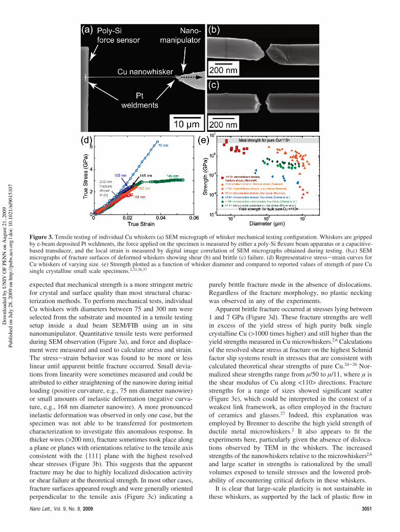
expected that mechanical strength is a more stringent metricfor crystal and surface quality than most structural charac-terization methods. To perform mechanical tests, individualCu whiskers with diameters between 75 and 300 nm wereselected from the substrate and mounted in a tensile testingsetup inside a dual beam SEM/FIB using an in situnanomanipulator. Quantitative tensile tests were performedduring SEM observation (Figure 3a), and force and displace-ment were measured and used to calculate stress and strain.The stress-strain behavior was found to be more or lesslinear until apparent brittle fracture occurred. Small devia-tions from linearity were sometimes measured and could beattributed to either straightening of the nanowire during initialloading (positive curvature, e.g., 75 nm diameter nanowire)or small amounts of inelastic deformation (negative curva-ture, e.g., 168 nm diameter nanowire). A more pronouncedinelastic deformation was observed in only one case, but thespecimen was not able to be transferred for postmortemcharacterization to investigate this anomalous response. Inthicker wires (>200 nm), fracture sometimes took place alonga plane or planes with orientations relative to the tensile axisconsistent with the {111} plane with the highest resolvedshear stresses (Figure 3b). This suggests that the apparentfracture may be due to highly localized dislocation activityor shear failure at the theoretical strength. In most other cases,fracture surfaces appeared rough and were generally orientedperpendicular to the tensile axis (Figure 3c) indicating a
purely brittle fracture mode in the absence of dislocations.Regardless of the fracture morphology, no plastic neckingwas observed in any of the experiments.
Apparent brittle fracture occurred at stresses lying between1 and 7 GPa (Figure 3d). These fracture strengths are wellin excess of the yield stress of high purity bulk singlecrystalline Cu (>1000 times higher) and still higher than theyield strengths measured in Cu microwhiskers.2,6 Calculationsof the resolved shear stress at fracture on the highest Schmidfactor slip systems result in stresses that are consistent withcalculated theoretical shear strengths of pure Cu.24-26 Nor-malized shear strengths range from µ/50 to µ/11, where µ isthe shear modulus of Cu along <110> directions. Fracturestrengths for a range of sizes showed significant scatter(Figure 3e), which could be interpreted in the context of aweakest link framework, as often employed in the fractureof ceramics and glasses.27 Indeed, this explanation wasemployed by Brenner to describe the high yield strength ofductile metal microwhiskers.2 It also appears to fit theexperiments here, particularly given the absence of disloca-tions observed by TEM in the whiskers. The increasedstrengths of the nanowhiskers relative to the microwhiskers2,6
and large scatter in strengths is rationalized by the smallvolumes exposed to tensile stresses and the lowered prob-ability of encountering critical defects in these whiskers.
It is clear that large-scale plasticity is not sustainable inthese whiskers, as supported by the lack of plastic flow in
Figure 3. Tensile testing of individual Cu whiskers (a) SEM micrograph of whisker mechanical testing configuration. Whiskers are grippedby e-beam deposited Pt weldments, the force applied on the specimen is measured by either a poly-Si flexure beam apparatus or a capacitive-based transducer, and the local strain is measured by digital image correlation of SEM micrographs obtained during testing. (b,c) SEMmicrographs of fracture surfaces of deformed whiskers showing shear (b) and brittle (c) failure. (d) Representative stress-strain curves forCu whiskers of varying size. (e) Strength plotted as a function of whisker diameter and compared to reported values of strength of pure Cusingle crystalline small scale specimens.2,33,36,37
Nano Lett., Vol. 9, No. 8, 2009 3051
Dow
nloa
ded
by U
NIV
OF
PEN
N o
n A
ugus
t 21,
200
9Pu
blish
ed o
n Ju
ly 2
8, 2
009
on h
ttp://
pubs
.acs
.org
| do
i: 10
.102
1/nl
9015
107
the stress strain curves, as well as postmortem TEMcharacterization showing an absence of stored dislocationsin fractured whiskers. These results are quite different fromthe results obtained from a series of small-scale experimentson face-centered cubic (fcc) single crystals of arguably lowercrystal quality, which demonstrate smaller strengths with lessscatter, and a clear size effect (“smaller is stronger”).28-33
This behavior has been attributed to constrained dislocationinteractions and geometrical limitations of source size forsamples with dimensions between around 200 nm and 10µm. For smaller samples, it is observed that dislocations runout of the samples,34,35 leaving dislocation nucleation the onlypossible process for controlling further deformation. Uponnucleating dislocations in these nanowhiskers with goodcrystal quality and thus few critical defects, the deformationis expected to occur heterogeneously, which is commensuratewith the absence of tensile necking. Slip will be localizedto one single crystal plane since no other flaws are in thevicinity that can trigger subsequent plastic deformation bythis activity. Presumably the strength of these small samplesis controlled by the strength of the flaws for nucleating newdislocations and will depend critically on the sample prepara-tion method.
We report a novel synthesis route for producing singlecrystalline, high-aspect ratio, defect-free nanostructures ofa variety of pure materials. A combination of electronmicroscopy techniques show that Cu nanowhiskers have nodetectable defects and crystal shapes that bear resemblanceto those formed during equilibrium growth. Novel anddirectly interpretable in situ mechanical experiments revealultrahigh strengths, which to our knowledge, are the highestever reported in Cu. The absence of large amounts ofplasticity, in contrast to that typically encountered in purefcc metals, and the very high mechanical strength areattributed to the small sizes and crystalline quality of thesenanowhiskers. Both factors are likely to influence otherphysical properties such as electrical and thermal conductiv-ity. An understanding of the fabrication and structuralconditions required to achieve such metal structures will haveimplications on the development of high performancematerials for nanotechnological applications.
Acknowledgment. K.H. and G.R. gratefully acknowledgeMr. Michael Pudleiner for carrying out the thermal evapora-tion of the materials and Mr. Reinhart Volker for magnetronsputtering of the C layers. Mr. Kersten Hahn is acknowledgedfor the operation of the energy filtered-TEM. They are alsomuch obliged to Professor Eduard Arzt for the possibilitythat part of this work was carried out as a master thesis inhis departments at the MPI fur Metallforschung and the
University of Stuttgart. D.S.G. acknowledges support froman Alexander von Humboldt Postdoctoral Fellowship.
Supporting Information Available: Experimental meth-ods (materials deposition, microstructure characterization, insitu tensile testing) and additional figures (nanowhiskers fromother materials, further microstructure characterizations). Thismaterial is available free of charge via the Internet at http://pubs.acs.org.
References(1) Hardy, H. K. Prog. Met. Phys. 1956, 6, 45–73.(2) Brenner, S. S. J. Appl. Phys. 1956, 27, 1484–1491.(3) DeBlois, R. W.; Graham, C. D. J. Appl. Phys. 1958, 29, 931–939.(4) Lutes, O. S. Phys. ReV. 1957, 105, 1451–1458.(5) Shoenberg, D. Nature 1959, 183, 171.(6) Brenner, S. S. Acta Met. 1956, 4, 62–74.(7) Wagner, R. S.; Ellis, W. C. Appl. Phys. Lett. 1964, 4, 89.(8) Duan, X.; Huang, Y.; Cui, Y.; Wang, J.; Lieber, C. M. Nature 2001,
409, 66–69.(9) Borgstrom, M.; Deppert, K.; Seifert, W. J. Cryst. Growth 2004, 260,
18–22.(10) Karim, S.; et al. Appl. Phys. A 2006, 84, 403–407.(11) Gomer, R. In Growth and Perfection of Crystals; Doremus, R. H.,
Roberts, B. W., Turnbull, D., Eds.; Wiley: New York, 1958; pp 126-133.
(12) Melmed, A. J.; Gomer, R. J. Chem. Phys. 1961, 34, 1802–1812.(13) Brenner, S. S.; Morelock, C. R. ReV. Sci. Instrum. 1957, 28, 652–
653.(14) Nittono, O.; Nagakura, S. Jpn. J. Appl. Phys. 1969, 8, 1180–1188.(15) Rodrıguez, A. M.; Bozzolo, G.; Ferrante, J. Surf. Sci. 1993, 289, 100–
126.(16) Sears, G. W. Acta Met. 1955, 3, 361–369.(17) Frank, F. C. Disc. Faraday Soc. 1949, 5, 48–54.(18) Wang, P. I.; Zhao, Y. P.; Wang, T. M.; Lu, T. M. Nanotechnology
2004, 15, 218–222.(19) Egelhoff, W. F.; Tibbetts, G. G. Phys. ReV. B 1979, 19, 5028–5035.(20) Hamilton, J. F.; Logel, P. C. Thin Solid Films 1973, 16, 49–63.(21) Mortimer, D. A.; Nicholas, M. J. Mater. Sci. 1970, 5, 149–155.(22) Ruth, V.; Hirth, J. P. J. Chem. Phys. 1964, 41, 3139–3149.(23) Inkson, B. J.; Dehm, G.; Peng, Y. Nanotechnology 2007, 18, 1–4.(24) Ogata, S.; Li, J.; Yip, S. Science 2002, 298, 807–811.(25) Roundy, D.; Krenn, C. R.; Marvin, L.; Cohen, M. L.; Morris, J. W.,
Jr. Phys. ReV. Lett. 1999, 82, 2713–2716.(26) Paxton, A. T.; Gumbsch, P.; Methfessel, M. Philos. Mag. Lett. 1991,
63, 267–274.(27) Weibull, W. Proc. R. Swedish Inst. Eng. Res. 1939, 151, 1–45.(28) Uchic, M. D.; Dimiduk, D. M.; Florando, J. N.; Nix, W. D. Science
2004, 305, 986–989.(29) Greer, J. R.; Oliver, W. C.; Nix, W. D. Acta Mater. 2005, 53, 1821–
1830.(30) Greer, J. R.; Oliver, W. C.; Nix, W. D. Acta Mater. 2006, 54, 1705.(31) Volkert, C. A.; Lilleodden, E. T. Philos. Mag. 2006, 86, 5567–5579.(32) Gruber, P. A.; Solenthaler, C.; Arzt, E.; Spolenak, R. Acta Mater.
2008, 56, 1876–1889.(33) Kiener, D.; Grosinger, W.; Dehm, G.; Pippan, R. Acta Mater. 2008,
56, 580–592.(34) Shan, Z. W.; Mishra, R. K.; Asif, S. A.; Warren, O. L.; Minor, A. M.
Nat. Mater. 2008, 7, 115–119.(35) Oh, S. H.; Legros, M.; Kiener, D.; Dehm, G. Nat. Mater. 2009, 8,
95–100.(36) Brenner, S. S. J. Appl. Phys. 1957, 28, 1023–1026.(37) Kiener, D.; Motz, C.; Schoberl, T.; Jenko, M.; Dehm, G. AdV. Eng.
Mater. 2006, 8, 1119–1125.
NL9015107
3052 Nano Lett., Vol. 9, No. 8, 2009
Dow
nloa
ded
by U
NIV
OF
PEN
N o
n A
ugus
t 21,
200
9Pu
blish
ed o
n Ju
ly 2
8, 2
009
on h
ttp://
pubs
.acs
.org
| do
i: 10
.102
1/nl
9015
107
Related Documents


![Crystals with Ultrahigh Piezoelectricityvixra.org/pdf/2001.0316v1.pdfCrystals with Ultrahigh Piezoelectricity ... smartphones to advanced microprocessors. [26] ... probabilistic smears](https://static.cupdf.com/doc/110x72/6045ca6abb58fa5d2f40bf63/crystals-with-ultrahigh-p-crystals-with-ultrahigh-piezoelectricity-smartphones.jpg)