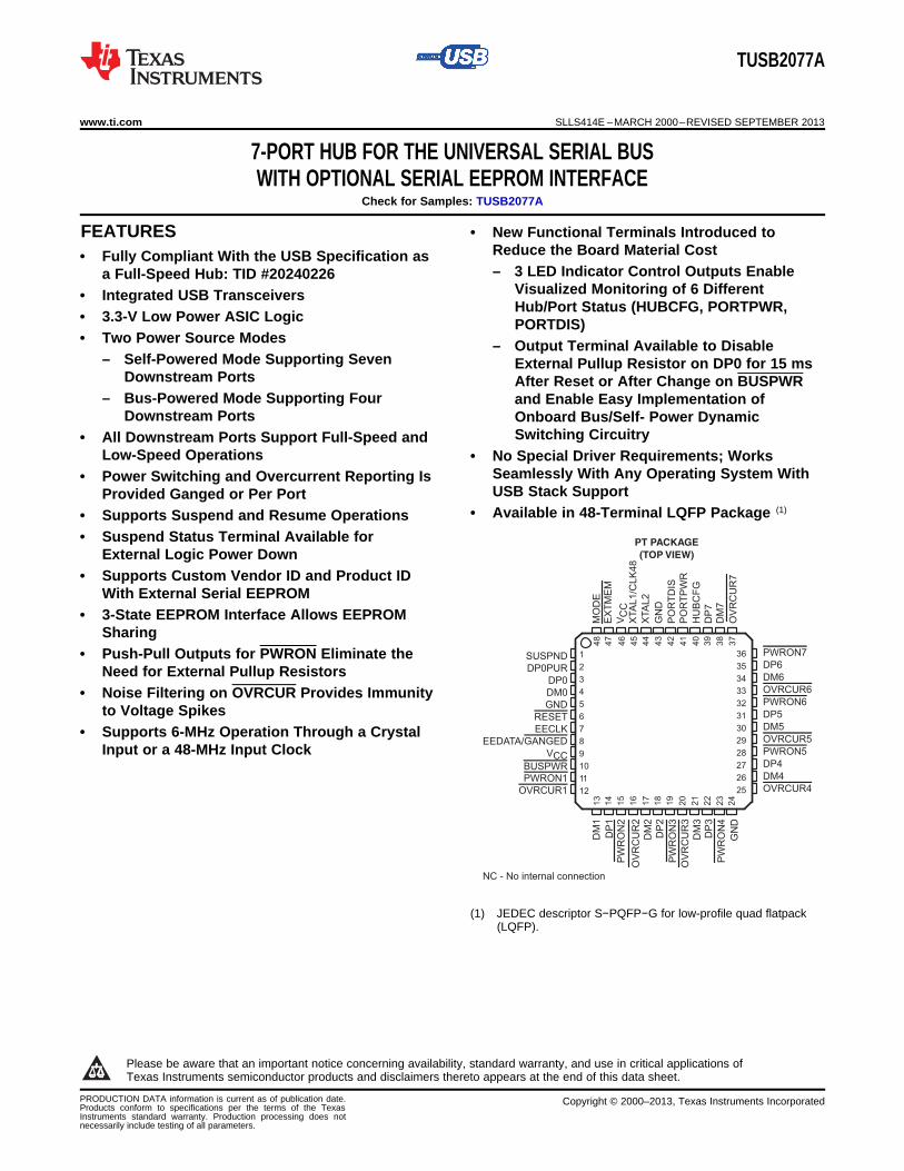
EXTMEM OVRCUR3 OVRCUR2 PWRON7 DP6 DM6 OVRCUR6 PWRON6 DP5 DM5 OVRCUR5 PWRON5 DP4 DM4 OVRCUR4 36 35 34 33 32 31 30 29 28 27 26 25 1 2 3 4 5 6 7 8 9 10 11 12 SUSPND DP0PUR DP0 DM0 GND RESET EECLK EEDATA/GANGED V CC BUSPWR PWRON1 OVRCUR1 HUBCFG DM7 MODE V XTAL1/CLK48 XTAL2 DP3 PWRON4 GND DM2 DP2 PWRON3 DM3 OVRCUR7 GND PORTPWR DP1 DM1 PT PACKAGE (TOP VIEW) 39 38 37 46 44 43 42 41 40 47 48 45 20 21 22 23 13 14 15 16 17 24 18 19 DP7 PORTDIS PWRON2 CC NC - No internal connection TUSB2077A www.ti.com SLLS414E – MARCH 2000 – REVISED SEPTEMBER 2013 7-PORT HUB FOR THE UNIVERSAL SERIAL BUS WITH OPTIONAL SERIAL EEPROM INTERFACE Check for Samples: TUSB2077A 1FEATURES • New Functional Terminals Introduced to Reduce the Board Material Cost • Fully Compliant With the USB Specification as – 3 LED Indicator Control Outputs Enable a Full-Speed Hub: TID #20240226 Visualized Monitoring of 6 Different • Integrated USB Transceivers Hub/Port Status (HUBCFG, PORTPWR, • 3.3-V Low Power ASIC Logic PORTDIS) • Two Power Source Modes – Output Terminal Available to Disable – Self-Powered Mode Supporting Seven External Pullup Resistor on DP0 for 15 ms Downstream Ports After Reset or After Change on BUSPWR – Bus-Powered Mode Supporting Four and Enable Easy Implementation of Downstream Ports Onboard Bus/Self- Power Dynamic Switching Circuitry • All Downstream Ports Support Full-Speed and Low-Speed Operations • No Special Driver Requirements; Works Seamlessly With Any Operating System With • Power Switching and Overcurrent Reporting Is USB Stack Support Provided Ganged or Per Port • Available in 48-Terminal LQFP Package (1) • Supports Suspend and Resume Operations • Suspend Status Terminal Available for External Logic Power Down • Supports Custom Vendor ID and Product ID With External Serial EEPROM • 3-State EEPROM Interface Allows EEPROM Sharing • Push-Pull Outputs for PWRON Eliminate the Need for External Pullup Resistors • Noise Filtering on OVRCUR Provides Immunity to Voltage Spikes • Supports 6-MHz Operation Through a Crystal Input or a 48-MHz Input Clock (1) JEDEC descriptor S−PQFP−G for low-profile quad flatpack (LQFP). xxx 1 Please be aware that an important notice concerning availability, standard warranty, and use in critical applications of Texas Instruments semiconductor products and disclaimers thereto appears at the end of this data sheet. PRODUCTION DATA information is current as of publication date. Copyright © 2000–2013, Texas Instruments Incorporated Products conform to specifications per the terms of the Texas Instruments standard warranty. Production processing does not necessarily include testing of all parameters.

Welcome message from author
This document is posted to help you gain knowledge. Please leave a comment to let me know what you think about it! Share it to your friends and learn new things together.
Transcript
EX
TM
EM
OV
RC
UR
3
OV
RC
UR
2
PWRON7
DP6
DM6
OVRCUR6
PWRON6
DP5
DM5
OVRCUR5
PWRON5
DP4
DM4
OVRCUR4
36
35
34
33
32
31
30
29
28
27
26
25
1
2
3
4
5
6
7
8
9
10
11
12
SUSPND
DP0PUR
DP0
DM0
GND
RESET
EECLK
EEDATA/GANGED
VCC
BUSPWR
PWRON1
OVRCUR1
HU
BC
FG
DM
7
MO
DE
V XTA
L1/C
LK
48
XTA
L2
DP
3
PW
RO
N4
GN
D
DM
2
DP
2
PW
RO
N3
DM
3
OV
RC
UR
7
GN
D
PO
RT
PW
R
DP
1
DM
1
PT PACKAGE
(TOP VIEW)
39
38
37
46
44
43
42
41
40
47
48
45
20
21
22
23
13
14
15
16
17
24
18
19
DP
7
PO
RT
DIS
PW
RO
N2
CC
NC - No internal connection
TUSB2077A
www.ti.com SLLS414E –MARCH 2000–REVISED SEPTEMBER 2013
7-PORT HUB FOR THE UNIVERSAL SERIAL BUSWITH OPTIONAL SERIAL EEPROM INTERFACE
Check for Samples: TUSB2077A
1FEATURES • New Functional Terminals Introduced toReduce the Board Material Cost• Fully Compliant With the USB Specification as– 3 LED Indicator Control Outputs Enablea Full-Speed Hub: TID #20240226
Visualized Monitoring of 6 Different• Integrated USB TransceiversHub/Port Status (HUBCFG, PORTPWR,• 3.3-V Low Power ASIC Logic PORTDIS)
• Two Power Source Modes – Output Terminal Available to Disable– Self-Powered Mode Supporting Seven External Pullup Resistor on DP0 for 15 ms
Downstream Ports After Reset or After Change on BUSPWR– Bus-Powered Mode Supporting Four and Enable Easy Implementation of
Downstream Ports Onboard Bus/Self- Power DynamicSwitching Circuitry• All Downstream Ports Support Full-Speed and
Low-Speed Operations • No Special Driver Requirements; WorksSeamlessly With Any Operating System With• Power Switching and Overcurrent Reporting IsUSB Stack SupportProvided Ganged or Per Port
• Available in 48-Terminal LQFP Package (1)• Supports Suspend and Resume Operations• Suspend Status Terminal Available for
External Logic Power Down• Supports Custom Vendor ID and Product ID
With External Serial EEPROM• 3-State EEPROM Interface Allows EEPROM
Sharing• Push-Pull Outputs for PWRON Eliminate the
Need for External Pullup Resistors• Noise Filtering on OVRCUR Provides Immunity
to Voltage Spikes• Supports 6-MHz Operation Through a Crystal
Input or a 48-MHz Input Clock
(1) JEDEC descriptor S−PQFP−G for low-profile quad flatpack(LQFP).xxx
1
Please be aware that an important notice concerning availability, standard warranty, and use in critical applications ofTexas Instruments semiconductor products and disclaimers thereto appears at the end of this data sheet.
PRODUCTION DATA information is current as of publication date. Copyright © 2000–2013, Texas Instruments IncorporatedProducts conform to specifications per the terms of the TexasInstruments standard warranty. Production processing does notnecessarily include testing of all parameters.
TUSB2077A
SLLS414E –MARCH 2000–REVISED SEPTEMBER 2013 www.ti.com
ORDERING INFORMATION (1)
TA PACKAGE (2) ORDERABLE PART NUMBER TOP-SIDE MARKINGReel of 250 TUSB2077APT
0°C to 70°C LQFP – PT TUSB2077APTR TUSB2077AReel of 1000
TUSB2077APTRG4
(1) Package drawings, standard packing quantities, thermal data, symbolization, and PCB design guidelines are available atwww.ti.com/sc/package.
(2) For the most current package and ordering information, see the Package Option Addendum at the end of this document, or see the TIwebsite at www.ti.com.
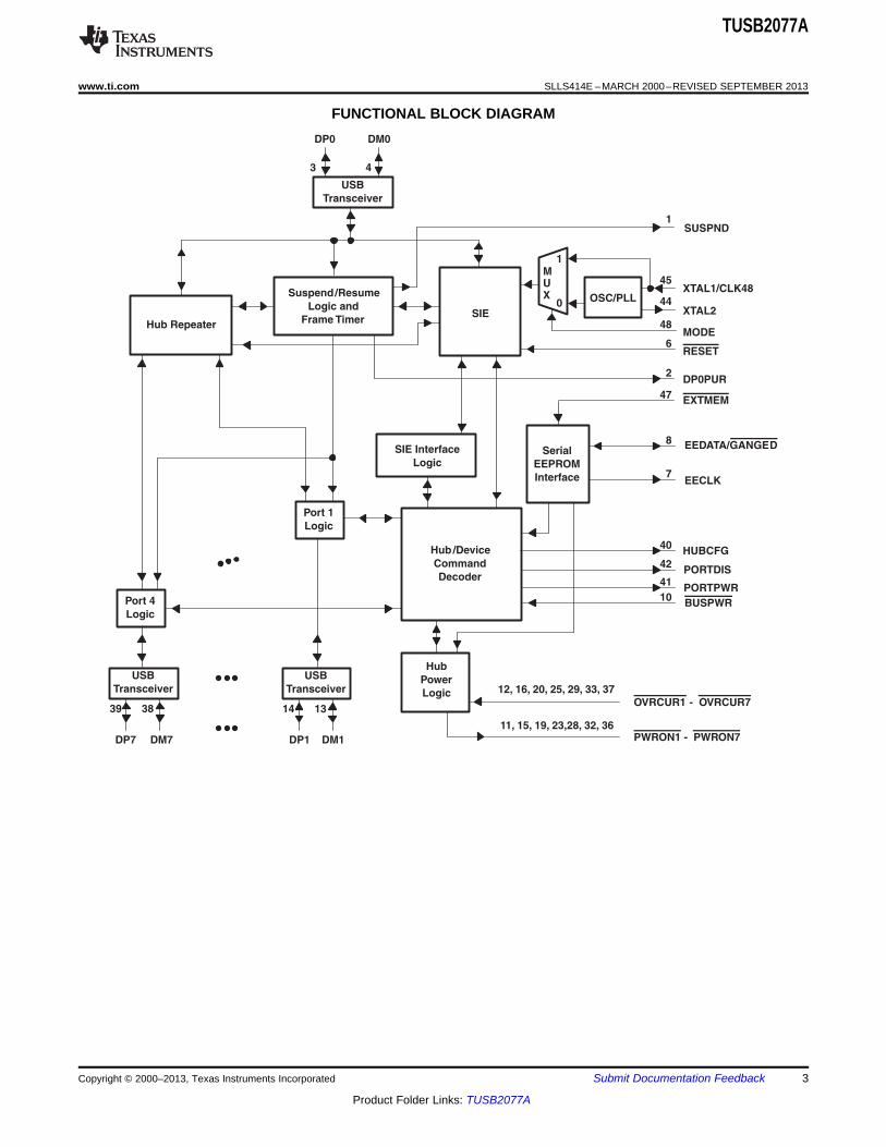
DESCRIPTIONThe TUSB2077A hub is a 3.3-V CMOS device that provides up to seven downstream ports in compliance withthe USB 2.0 specification. Because this device is implemented with a digital state machine instead of amicrocontroller, no software programming is required. Fully-compliant USB transceivers are integrated into theASIC for all upstream and downstream ports. The downstream ports support both full-speed and low-speeddevices by automatically setting the slew rate according to the speed of the device attached to the ports. Theconfiguration of the BUSPWR terminal selects either the bus-powered or self-powered mode. The introduction ofthe DP0 pullup resistor disable terminal, DP0PUR, makes it much easier to implement an onboard bus/self-power dynamic-switching circuitry. The three LED indicator control output terminals also enable theimplementation of visualized status monitoring of the hub and its downstream ports. With these new functionterminals, the end equipment vendor can considerably reduce the total board cost while adding additionalproduct value.
The EXTMEM (terminal 47) enables or disables the optional EEPROM interface. When EXTMEM is high, thevendor and product IDs (VID and PID) use defaults, such that the message displayed during enumeration isGeneral Purpose USB Hub. For this configuration, terminal 8 functions as the GANGED input terminal andEECLK (terminal 7) is unused. If custom VID and PID descriptors are desired, the EXTMEM must be tied low(EXTMEM = 0) and a SGS Thompson M93C46 EEPROM, or equivalent, stores the programmable VID, PID, andGANGED values. For this configuration, terminals 7 and 8 function as the EEPROM interface signals withterminal 7 as EECLK and terminal 8 as EEDATA, respectively.
The TUSB2077A supports both bus-powered and self-powered modes. External power-management devices,such as the TPS2044, are required to control the 5-V power source switching (on/off) to the downstream portsand to detect an overcurrent condition from the downstream ports individually or ganged. Outputs from externalpower devices provide overcurrent inputs to the TUSB2077A OVRCUR terminals in case of an overcurrentcondition, the corresponding PWRON terminals are disabled by the TUSB2077A. In the ganged mode, allPWRON signals transition simultaneously, and any OVRCUR input can be used. In the nonganged mode, thePWROR outputs and OVRCUR inputs operate on a per-port basis.
The TUSB2077A provides the flexibility of using either a 6-MHz or a 48-MHz clock. The logic level of the MODEterminal controls the selection of the clock source. When MODE is low, the output of the internal APLL circuitry isselected to drive the internal core of the chip. When MODE is high, the XTAL1 input is selected as the inputclock source and the APLL circuitry is powered down and bypassed. The internal oscillator cell is also powereddown while MODE is high. For 6-MHz operation, TUSB2077A requires a 6-MHz clock signal on XTAL1 terminal(with XTAL2 for a crystal) from which its internal APLL circuitry generates a 48-MHz internal clock to sample thedata from the upstream port. For 48-MHz operation, the clock cannot be generated with a crystal, using theXTAL2 output, since the internal oscillator cell only supports the fundamental frequency. If low-power suspendand resume are desired, a passive crystal or resonator must be used, although the hub supports the flexibility ofusing any device that generates a 6-MHz clock. Because most oscillators cannot be stopped while power is on,their use prohibits low-power suspend, which depends on disabling the clock. When the oscillator is used, byconnecting its output to the XTAL1 terminal and leaving the XTAL2 terminal open, its TTL output level can notexceed 3.6 V. If a 6-MHz oscillator is used, it must be stopped at logic low whenever SUSPND is high. Forcrystal or resonator implementations, the XTAL1 terminal is the input and the XTAL2 terminal is used as thefeedback path. A sample crystal tuning circuit is shown in Figure 7.
2 Submit Documentation Feedback Copyright © 2000–2013, Texas Instruments Incorporated
Product Folder Links: TUSB2077A
45
6
47
8
7
Hub Repeater
Suspend/Resume
Logic and
Frame TimerSIE
SIE Interface
Logic
Port 1
Logic
Hub/Device
Command
Decoder
Hub
Power
LogicOVRCUR1 - OVRCUR7
PWRON1 - PWRON7
XTAL1/CLK48OSC/PLL
DP0 DM0
3 4
USB
Transceiver
DP7 DM7 DP1 DM1
14 13
12, 16, 20, 25, 29, 33, 37
11, 15, 19, 23,28, 32, 36
RESET
USB
Transceiver
Serial
EEPROM
Interface
EXTMEM
EEDATA/GANGED
EECLK
USB
Transceiver
39 38
Port 4
Logic
10BUSPWR
1SUSPND
41PORTPWR
42PORTDIS
40HUBCFG
MODE
MUX
44XTAL2
1
0
48
2DP0PUR
TUSB2077A
www.ti.com SLLS414E –MARCH 2000–REVISED SEPTEMBER 2013
FUNCTIONAL BLOCK DIAGRAM
Copyright © 2000–2013, Texas Instruments Incorporated Submit Documentation Feedback 3
Product Folder Links: TUSB2077A
TUSB2077A
SLLS414E –MARCH 2000–REVISED SEPTEMBER 2013 www.ti.com
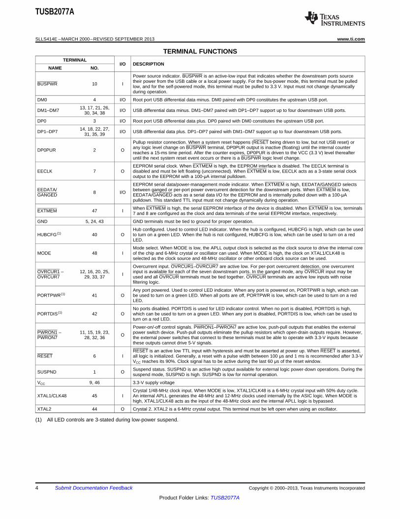
TERMINAL FUNCTIONSTERMINAL
I/O DESCRIPTIONNAME NO.
Power source indicator. BUSPWR is an active-low input that indicates whether the downstream ports sourcetheir power from the USB cable or a local power supply. For the bus-power mode, this terminal must be pulledBUSPWR 10 I low, and for the self-powered mode, this terminal must be pulled to 3.3 V. Input must not change dynamicallyduring operation.
DM0 4 I/O Root port USB differential data minus. DM0 paired with DP0 constitutes the upstream USB port.
13, 17, 21, 26,DM1–DM7 I/O USB differential data minus. DM1–DM7 paired with DP1–DP7 support up to four downstream USB ports.30, 34, 38
DP0 3 I/O Root port USB differential data plus. DP0 paired with DM0 constitutes the upstream USB port.
14, 18, 22, 27,DP1–DP7 I/O USB differential data plus. DP1–DP7 paired with DM1–DM7 support up to four downstream USB ports.31, 35, 39
Pullup resistor connection. When a system reset happens (RESET being driven to low, but not USB reset) orany logic level change on BUSPWR terminal, DP0PUR output is inactive (floating) until the internal counterDP0PUR 2 O reaches a 15-ms time period. After the counter expires, DP0PUR is driven to the VCC (3.3 V) level thereafteruntil the next system reset event occurs or there is a BUSPWR logic level change.
EEPROM serial clock. When EXTMEM is high, the EEPROM interface is disabled. The EECLK terminal isEECLK 7 O disabled and must be left floating (unconnected). When EXTMEM is low, EECLK acts as a 3-state serial clock
output to the EEPROM with a 100-μA internal pulldown.
EEPROM serial data/power-management mode indicator. When EXTMEM is high, EEDATA/GANGED selectsEEDATA/ between ganged or per-port power overcurrent detection for the downstream ports. When EXTMEM is low,8 I/OGANGED EEDATA/GANGED acts as a serial data I/O for the EEPROM and is internally pulled down with a 100-μA
pulldown. This standard TTL input must not change dynamically during operation.
When EXTMEM is high, the serial EEPROM interface of the device is disabled. When EXTMEM is low, terminalsEXTMEM 47 I 7 and 8 are configured as the clock and data terminals of the serial EEPROM interface, respectively.
GND 5, 24, 43 GND terminals must be tied to ground for proper operation.
Hub configured. Used to control LED indicator. When the hub is configured, HUBCFG is high, which can be usedHUBCFG (1) 40 O to turn on a green LED. When the hub is not configured, HUBCFG is low, which can be used to turn on a red
LED.
Mode select. When MODE is low, the APLL output clock is selected as the clock source to drive the internal coreMODE 48 I of the chip and 6-MHz crystal or oscillator can used. When MODE is high, the clock on XTAL1/CLK48 is
selected as the clock source and 48-MHz oscillator or other onboard clock source can be used.
Overcurrent input. OVRCUR1–OVRCUR7 are active low. For per-port overcurrent detection, one overcurrentOVRCUR1 – 12, 16, 20, 25, input is available for each of the seven downstream ports. In the ganged mode, any OVRCUR input may beIOVRCUR7 29, 33, 37 used and all OVRCUR terminals must be tied together. OVRCUR terminals are active low inputs with noise
filtering logic.
Any port powered. Used to control LED indicator. When any port is powered on, PORTPWR is high, which canPORTPWR (1) 41 O be used to turn on a green LED. When all ports are off, PORTPWR is low, which can be used to turn on a red
LED.
No ports disabled. PORTDIS is used for LED indicator control. When no port is disabled, PORTDIS is high,PORTDIS (1) 42 O which can be used to turn on a green LED. When any port is disabled, PORTDIS is low, which can be used to
turn on a red LED.
Power-on/-off control signals. PWRON1–PWRON7 are active low, push-pull outputs that enables the externalPWRON1 – 11, 15, 19, 23, power switch device. Push-pull outputs eliminate the pullup resistors which open-drain outputs require. However,OPWRON7 28, 32, 36 the external power switches that connect to these terminals must be able to operate with 3.3-V inputs because
these outputs cannot drive 5-V signals.
RESET is an active low TTL input with hysteresis and must be asserted at power up. When RESET is asserted,RESET 6 I all logic is initialized. Generally, a reset with a pulse width between 100 μs and 1 ms is recommended after 3.3-V
VCC reaches its 90%. Clock signal has to be active during the last 60 μs of the reset window.
Suspend status. SUSPND is an active high output available for external logic power-down operations. During theSUSPND 1 O suspend mode, SUSPND is high. SUSPND is low for normal operation.
VCC 9, 46 3.3-V supply voltage
Crystal 1/48-MHz clock input. When MODE is low, XTAL1/CLK48 is a 6-MHz crystal input with 50% duty cycle.XTAL1/CLK48 45 I An internal APLL generates the 48-MHz and 12-MHz clocks used internally by the ASIC logic. When MODE is
high, XTAL1/CLK48 acts as the input of the 48-MHz clock and the internal APLL logic is bypassed.
XTAL2 44 O Crystal 2. XTAL2 is a 6-MHz crystal output. This terminal must be left open when using an oscillator.
(1) All LED controls are 3-stated during low-power suspend.
4 Submit Documentation Feedback Copyright © 2000–2013, Texas Instruments Incorporated
Product Folder Links: TUSB2077A
TUSB2077A
www.ti.com SLLS414E –MARCH 2000–REVISED SEPTEMBER 2013
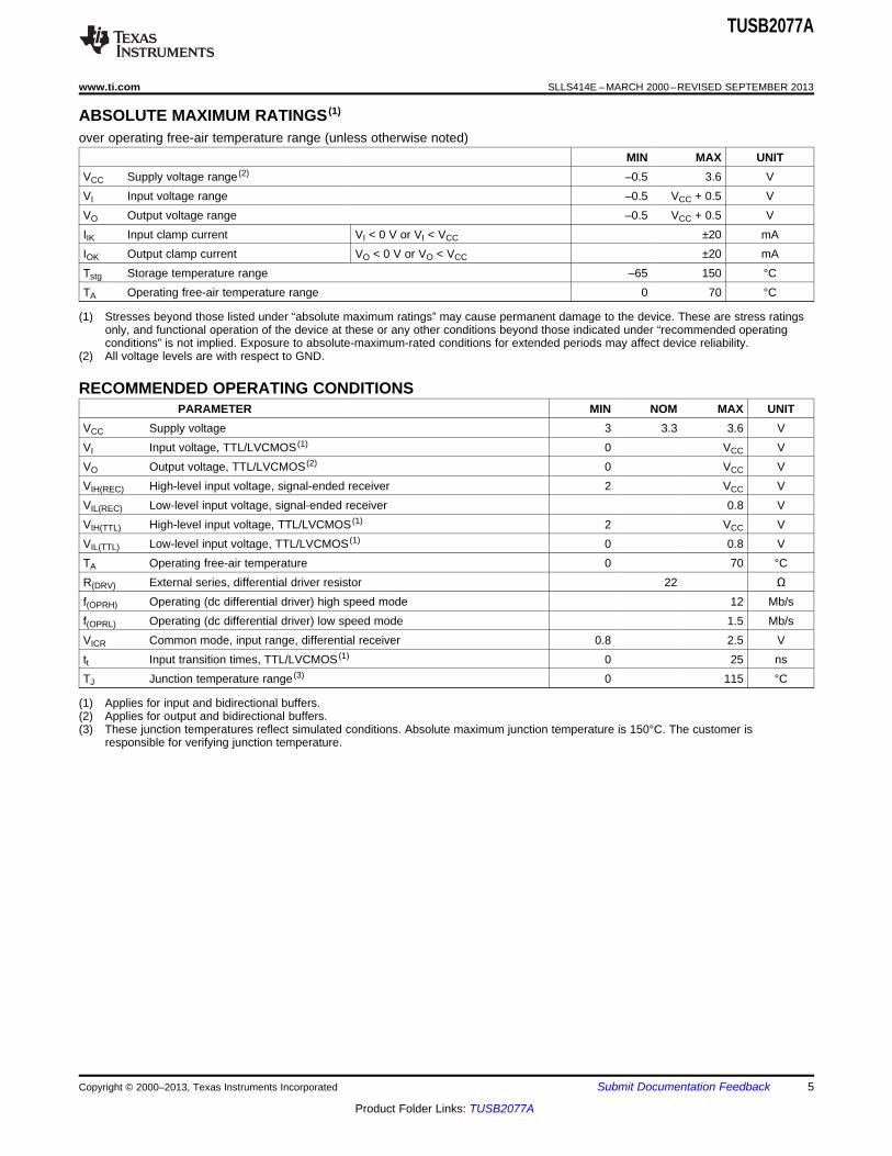
ABSOLUTE MAXIMUM RATINGS (1)
over operating free-air temperature range (unless otherwise noted)MIN MAX UNIT
VCC Supply voltage range (2) –0.5 3.6 VVI Input voltage range –0.5 VCC + 0.5 VVO Output voltage range –0.5 VCC + 0.5 VIIK Input clamp current VI < 0 V or VI < VCC ±20 mAIOK Output clamp current VO < 0 V or VO < VCC ±20 mATstg Storage temperature range –65 150 °CTA Operating free-air temperature range 0 70 °C
(1) Stresses beyond those listed under “absolute maximum ratings” may cause permanent damage to the device. These are stress ratingsonly, and functional operation of the device at these or any other conditions beyond those indicated under “recommended operatingconditions” is not implied. Exposure to absolute-maximum-rated conditions for extended periods may affect device reliability.
(2) All voltage levels are with respect to GND.
RECOMMENDED OPERATING CONDITIONSPARAMETER MIN NOM MAX UNIT
VCC Supply voltage 3 3.3 3.6 VVI Input voltage, TTL/LVCMOS (1) 0 VCC VVO Output voltage, TTL/LVCMOS (2) 0 VCC VVIH(REC) High-level input voltage, signal-ended receiver 2 VCC VVIL(REC) Low-level input voltage, signal-ended receiver 0.8 VVIH(TTL) High-level input voltage, TTL/LVCMOS (1) 2 VCC VVIL(TTL) Low-level input voltage, TTL/LVCMOS (1) 0 0.8 VTA Operating free-air temperature 0 70 °CR(DRV) External series, differential driver resistor 22 Ωf(OPRH) Operating (dc differential driver) high speed mode 12 Mb/sf(OPRL) Operating (dc differential driver) low speed mode 1.5 Mb/sVICR Common mode, input range, differential receiver 0.8 2.5 Vtt Input transition times, TTL/LVCMOS (1) 0 25 nsTJ Junction temperature range (3) 0 115 °C
(1) Applies for input and bidirectional buffers.(2) Applies for output and bidirectional buffers.(3) These junction temperatures reflect simulated conditions. Absolute maximum junction temperature is 150°C. The customer is
responsible for verifying junction temperature.
Copyright © 2000–2013, Texas Instruments Incorporated Submit Documentation Feedback 5
Product Folder Links: TUSB2077A
TUSB2077A
SLLS414E –MARCH 2000–REVISED SEPTEMBER 2013 www.ti.com
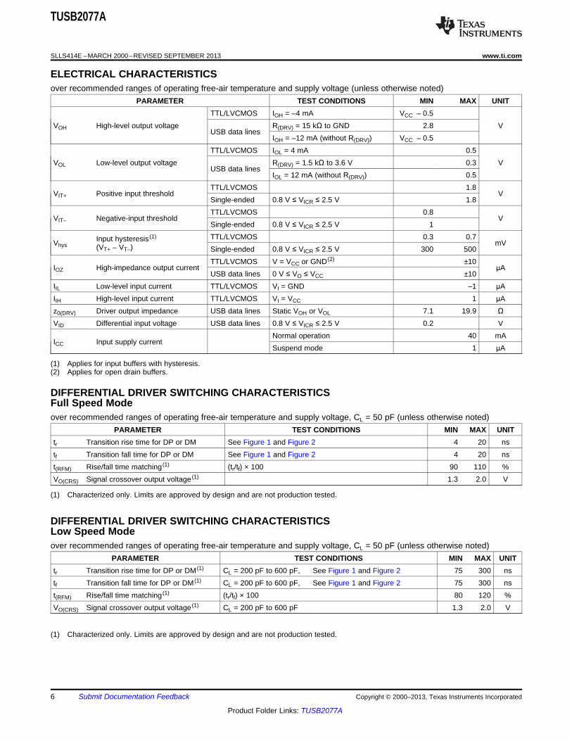
ELECTRICAL CHARACTERISTICSover recommended ranges of operating free-air temperature and supply voltage (unless otherwise noted)
PARAMETER TEST CONDITIONS MIN MAX UNITTTL/LVCMOS IOH = –4 mA VCC – 0.5
VOH High-level output voltage R(DRV) = 15 kΩ to GND 2.8 VUSB data lines
IOH = –12 mA (without R(DRV)) VCC – 0.5TTL/LVCMOS IOL = 4 mA 0.5
VOL Low-level output voltage R(DRV) = 1.5 kΩ to 3.6 V 0.3 VUSB data lines
IOL = 12 mA (without R(DRV)) 0.5TTL/LVCMOS 1.8
VIT+ Positive input threshold VSingle-ended 0.8 V ≤ VICR ≤ 2.5 V 1.8TTL/LVCMOS 0.8
VIT– Negative-input threshold VSingle-ended 0.8 V ≤ VICR ≤ 2.5 V 1TTL/LVCMOS 0.3 0.7Input hysteresis (1)
Vhys mV(VT+ – VT–) Single-ended 0.8 V ≤ VICR ≤ 2.5 V 300 500TTL/LVCMOS V = VCC or GND (2) ±10
IOZ High-impedance output current μAUSB data lines 0 V ≤ VO ≤ VCC ±10
IIL Low-level input current TTL/LVCMOS VI = GND –1 μAIIH High-level input current TTL/LVCMOS VI = VCC 1 μAz0(DRV) Driver output impedance USB data lines Static VOH or VOL 7.1 19.9 ΩVID Differential input voltage USB data lines 0.8 V ≤ VICR ≤ 2.5 V 0.2 V
Normal operation 40 mAICC Input supply current
Suspend mode 1 μA
(1) Applies for input buffers with hysteresis.(2) Applies for open drain buffers.
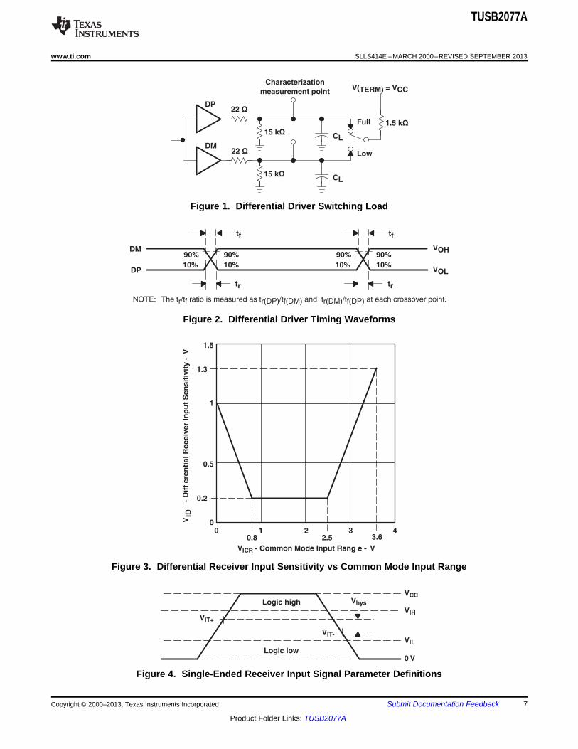
DIFFERENTIAL DRIVER SWITCHING CHARACTERISTICSFull Speed Modeover recommended ranges of operating free-air temperature and supply voltage, CL = 50 pF (unless otherwise noted)
PARAMETER TEST CONDITIONS MIN MAX UNITtr Transition rise time for DP or DM See Figure 1 and Figure 2 4 20 nstf Transition fall time for DP or DM See Figure 1 and Figure 2 4 20 nst(RFM) Rise/fall time matching (1) (tr/tf) × 100 90 110 %VO(CRS) Signal crossover output voltage (1) 1.3 2.0 V
(1) Characterized only. Limits are approved by design and are not production tested.
DIFFERENTIAL DRIVER SWITCHING CHARACTERISTICSLow Speed Modeover recommended ranges of operating free-air temperature and supply voltage, CL = 50 pF (unless otherwise noted)
PARAMETER TEST CONDITIONS MIN MAX UNITtr Transition rise time for DP or DM (1) CL = 200 pF to 600 pF, See Figure 1 and Figure 2 75 300 nstf Transition fall time for DP or DM (1) CL = 200 pF to 600 pF, See Figure 1 and Figure 2 75 300 nst(RFM) Rise/fall time matching (1) (tr/tf) × 100 80 120 %VO(CRS) Signal crossover output voltage (1) CL = 200 pF to 600 pF 1.3 2.0 V
(1) Characterized only. Limits are approved by design and are not production tested.
6 Submit Documentation Feedback Copyright © 2000–2013, Texas Instruments Incorporated
Product Folder Links: TUSB2077A
Vhys
VIT+
VIT-
VCC
VIH
VIL
0 V
Logic high
Logic low
0.5
00 1 2
- D
iff
ere
nti
al R
eceiv
er
Inp
ut
Sen
sit
ivit
y -
V
1
1.5
3 4
VID
VICR - Common Mode Input Rang e - V
0.8 3.6
0.2
1.3
2.5
15 kΩ
15 kΩ
1.5 kΩ
22 Ω
22 Ω
TUSB2077A
www.ti.com SLLS414E –MARCH 2000–REVISED SEPTEMBER 2013
Figure 1. Differential Driver Switching Load
Figure 2. Differential Driver Timing Waveforms
Figure 3. Differential Receiver Input Sensitivity vs Common Mode Input Range
Figure 4. Single-Ended Receiver Input Signal Parameter Definitions
Copyright © 2000–2013, Texas Instruments Incorporated Submit Documentation Feedback 7
Product Folder Links: TUSB2077A
PrinterWith 4-Port Hub(Self-Powered)
Scanner DigitalScanner
PCWith Root Hub
MonitorWith 4-Port Hub (Self-Powered)
TUSB2077A
SLLS414E –MARCH 2000–REVISED SEPTEMBER 2013 www.ti.com
APPLICATION INFORMATION
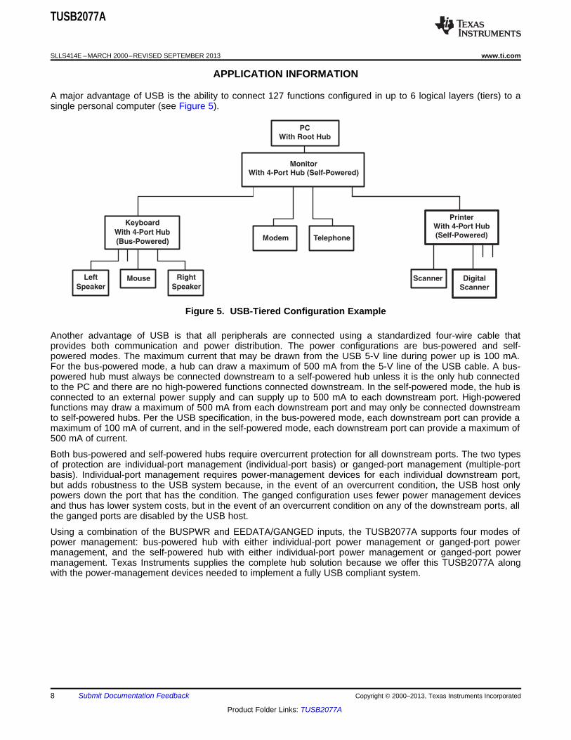
A major advantage of USB is the ability to connect 127 functions configured in up to 6 logical layers (tiers) to asingle personal computer (see Figure 5).
Figure 5. USB-Tiered Configuration Example
Another advantage of USB is that all peripherals are connected using a standardized four-wire cable thatprovides both communication and power distribution. The power configurations are bus-powered and self-powered modes. The maximum current that may be drawn from the USB 5-V line during power up is 100 mA.For the bus-powered mode, a hub can draw a maximum of 500 mA from the 5-V line of the USB cable. A bus-powered hub must always be connected downstream to a self-powered hub unless it is the only hub connectedto the PC and there are no high-powered functions connected downstream. In the self-powered mode, the hub isconnected to an external power supply and can supply up to 500 mA to each downstream port. High-poweredfunctions may draw a maximum of 500 mA from each downstream port and may only be connected downstreamto self-powered hubs. Per the USB specification, in the bus-powered mode, each downstream port can provide amaximum of 100 mA of current, and in the self-powered mode, each downstream port can provide a maximum of500 mA of current.
Both bus-powered and self-powered hubs require overcurrent protection for all downstream ports. The two typesof protection are individual-port management (individual-port basis) or ganged-port management (multiple-portbasis). Individual-port management requires power-management devices for each individual downstream port,but adds robustness to the USB system because, in the event of an overcurrent condition, the USB host onlypowers down the port that has the condition. The ganged configuration uses fewer power management devicesand thus has lower system costs, but in the event of an overcurrent condition on any of the downstream ports, allthe ganged ports are disabled by the USB host.
Using a combination of the BUSPWR and EEDATA/GANGED inputs, the TUSB2077A supports four modes ofpower management: bus-powered hub with either individual-port power management or ganged-port powermanagement, and the self-powered hub with either individual-port power management or ganged-port powermanagement. Texas Instruments supplies the complete hub solution because we offer this TUSB2077A alongwith the power-management devices needed to implement a fully USB compliant system.
8 Submit Documentation Feedback Copyright © 2000–2013, Texas Instruments Incorporated
Product Folder Links: TUSB2077A
XTAL1
C1 C2
CL
XTAL2
1 kΩ
DP0
DM0
EEDATA
TUSB2077A USB Hub
System
Power-On Reset
Regulator
Power
Switching
OVRCUR1 –
OVRCUR7
PWRON1 –
PWRON7
EECLK
RESET
XTAL1
EXTMEM
VCC
GND
DP1 - DP7
DM1 - DM7
GND
Vbus
5 V GND
XTAL2
USB Data lines
and Power to
Downstream
Ports
Bus or Local Power6-MHz Clock
Signal
7
7
7
7
45
44
6
3
4
8
7
9, 46
5, 24, 43
14, 18, 22, 27, 31, 35, 39
12, 16, 20, 25, 29, 33, 37
13, 17, 21, 26, 30, 34, 38
11, 15, 19, 23, 28, 32, 36
5
8
6
2
4
3ORG
VCC
VSS
D
Q
C
S
1
EEPROM
3.3 V
47
TUSB2077A
www.ti.com SLLS414E –MARCH 2000–REVISED SEPTEMBER 2013
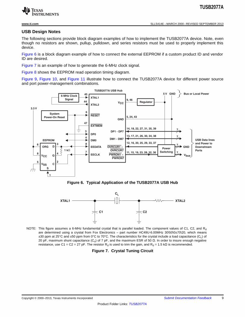
USB Design NotesThe following sections provide block diagram examples of how to implement the TUSB2077A device. Note, eventhough no resistors are shown, pullup, pulldown, and series resistors must be used to properly implement thisdevice.
Figure 6 is a block diagram example of how to connect the external EEPROM if a custom product ID and vendorID are desired.
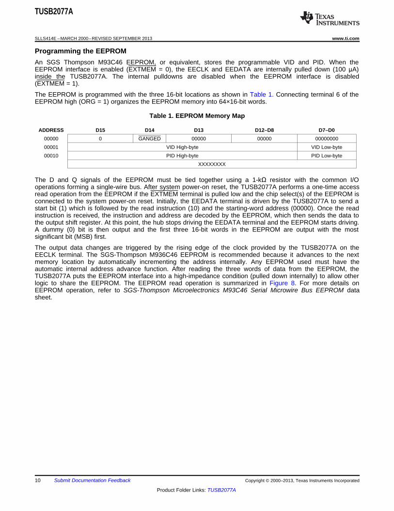
Figure 7 is an example of how to generate the 6-MHz clock signal.
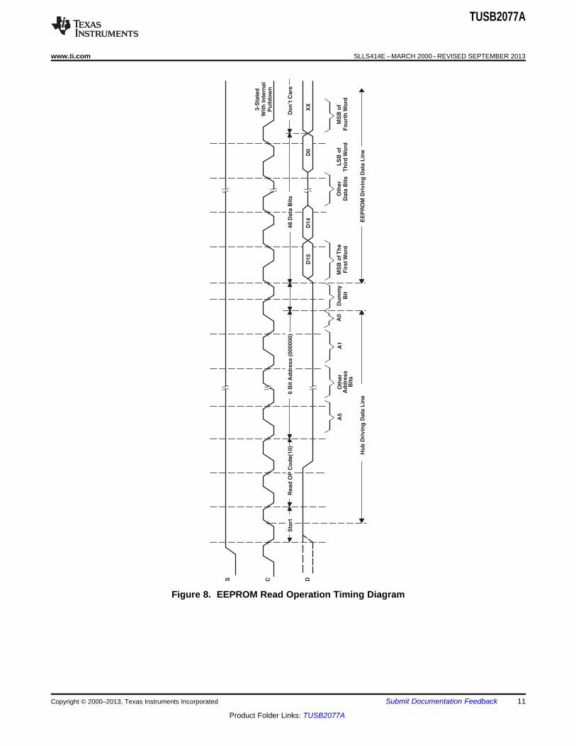
Figure 8 shows the EEPROM read operation timing diagram.
Figure 9, Figure 10, and Figure 11 illustrate how to connect the TUSB2077A device for different power sourceand port power-management combinations.
Figure 6. Typical Application of the TUSB2077A USB Hub
NOTE: This figure assumes a 6-MHz fundamental crystal that is parallel loaded. The component values of C1, C2, and Rdare determined using a crystal from Fox Electronics – part number HC49U-6.00MHz 30\50\0±70\20, which means±30 ppm at 25°C and ±50 ppm from 0°C to 70°C. The characteristics for the crystal include a load capacitance (CL) of20 pF, maximum shunt capacitance (Co) of 7 pF, and the maximum ESR of 50 Ω. In order to insure enough negativeresistance, use C1 = C2 = 27 pF. The resistor Rd is used to trim the gain, and Rd = 1.5 kΩ is recommended.
Figure 7. Crystal Tuning Circuit
Copyright © 2000–2013, Texas Instruments Incorporated Submit Documentation Feedback 9
Product Folder Links: TUSB2077A
TUSB2077A
SLLS414E –MARCH 2000–REVISED SEPTEMBER 2013 www.ti.com
Programming the EEPROMAn SGS Thompson M93C46 EEPROM, or equivalent, stores the programmable VID and PID. When theEEPROM interface is enabled (EXTMEM = 0), the EECLK and EEDATA are internally pulled down (100 μA)inside the TUSB2077A. The internal pulldowns are disabled when the EEPROM interface is disabled(EXTMEM = 1).
The EEPROM is programmed with the three 16-bit locations as shown in Table 1. Connecting terminal 6 of theEEPROM high (ORG = 1) organizes the EEPROM memory into 64×16-bit words.
Table 1. EEPROM Memory Map
ADDRESS D15 D14 D13 D12–D8 D7–D000000 0 GANGED 00000 00000 0000000000001 VID High-byte VID Low-byte00010 PID High-byte PID Low-byte
XXXXXXXX
The D and Q signals of the EEPROM must be tied together using a 1-kΩ resistor with the common I/Ooperations forming a single-wire bus. After system power-on reset, the TUSB2077A performs a one-time accessread operation from the EEPROM if the EXTMEM terminal is pulled low and the chip select(s) of the EEPROM isconnected to the system power-on reset. Initially, the EEDATA terminal is driven by the TUSB2077A to send astart bit (1) which is followed by the read instruction (10) and the starting-word address (00000). Once the readinstruction is received, the instruction and address are decoded by the EEPROM, which then sends the data tothe output shift register. At this point, the hub stops driving the EEDATA terminal and the EEPROM starts driving.A dummy (0) bit is then output and the first three 16-bit words in the EEPROM are output with the mostsignificant bit (MSB) first.
The output data changes are triggered by the rising edge of the clock provided by the TUSB2077A on theEECLK terminal. The SGS-Thompson M936C46 EEPROM is recommended because it advances to the nextmemory location by automatically incrementing the address internally. Any EEPROM used must have theautomatic internal address advance function. After reading the three words of data from the EEPROM, theTUSB2077A puts the EEPROM interface into a high-impedance condition (pulled down internally) to allow otherlogic to share the EEPROM. The EEPROM read operation is summarized in Figure 8. For more details onEEPROM operation, refer to SGS-Thompson Microelectronics M93C46 Serial Microwire Bus EEPROM datasheet.
10 Submit Documentation Feedback Copyright © 2000–2013, Texas Instruments Incorporated
Product Folder Links: TUSB2077A
6 B
itA
dd
ress (
000000)
Sta
rtR
ead
OP
Co
de(1
0)
48 D
ata
Bit
sD
on
’t C
are
D15
D14
D0
XX
A5
A1
A0
Du
mm
yB
itM
SB
ofT
he
Fir
stW
ord
Oth
er
Data
Bit
sL
SB
of
Th
ird
Wo
rdM
SB
of
Fo
urt
hW
ord
EE
PR
OM
Dri
vin
g D
ata
Lin
eH
ub
Dri
vin
g D
ata
Lin
e
3-S
tate
dW
ith
In
tern
al
Pu
lld
ow
n
S C D
Oth
er
Ad
dre
ss
Bit
s
TUSB2077A
www.ti.com SLLS414E –MARCH 2000–REVISED SEPTEMBER 2013
Figure 8. EEPROM Read Operation Timing Diagram
Copyright © 2000–2013, Texas Instruments Incorporated Submit Documentation Feedback 11
Product Folder Links: TUSB2077A
DP1
DM1
DP2
DM2
DP3
DM3
DP4
PWRON1
PWRON2
PWRON3
PWRON4
OVRCUR1
OVRCUR2
OVRCUR3
OVRCUR4
DM4
DP0
DM0
VCC
XTAL1
XTAL2
EXTMEM
RESET
SN75240†
EN IN
OC
OUT
D +
D -
5 V
GND
D +
D -
5 V
D +
D -
5 V
D +
D -
5 V
Downstream
Ports
TUSB2077A
TPS2041†
A
B
C
D
100 mF‡
SN75240†
A
B
C
D
GND
GND
GND
1 mF
100 mF‡
100 mF‡
100 mF‡
5 V
3.3 V
GND
D +
D -
Upstream
Port
3.3 V LDO§
SN75240†
A
B
5 V
GND
C
D
4.7 mF0.1 mF
4.7 mF
GND
Ferrite Beads
Ferrite Beads
Ferrite Beads
Ferrite Beads
EEDATA/GANGED
6-MHz Clock
Signal
BUSPWR
System
Power-On Reset
OUT
OUT
IN
3.3 V
1.5 kΩ
15 kΩ
15 kΩ
15 kΩ
15 kΩ
15 kΩ
15 kΩ
15 kΩ
15 kΩ
DP5 - DP7DM5 - DM7
PWRON5 -7
OVRCUR5 -7
NC
3.3 V
MODE
DP0PUR
¶
NOTES:
LDO is a 5-V-to-3.3-V voltage regulatorAll USB DP, DM signal pairs require series resistors of approximately 27
†
¶
TPS2041 and SN75240 are Texas Instruments devices.120 µF per hub is the minimum required per the USB specification. However, TI recommends a 100-µF, low ESR,tantalum capacitor per port for immunity to voltage droop.
‡
§Ω to ensure proper termination. An optional filter
capacitor of about 22 pF is recommended for EMI suppression. This capacitor, if used, must be placed between the hubterminal and the series resistor, as per section 7.1.6 of the USB specification.
TUSB2077A
SLLS414E –MARCH 2000–REVISED SEPTEMBER 2013 www.ti.com
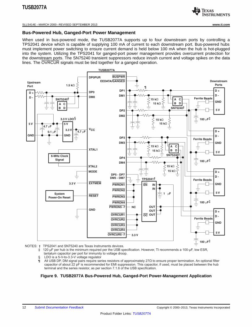
Bus-Powered Hub, Ganged-Port Power ManagementWhen used in bus-powered mode, the TUSB2077A supports up to four downstream ports by controlling aTPS2041 device which is capable of supplying 100 mA of current to each downstream port. Bus-powered hubsmust implement power switching to ensure current demand is held below 100 mA when the hub is hot-pluggedinto the system. Utilizing the TPS2041 for ganged-port power management provides overcurrent protection forthe downstream ports. The SN75240 transient suppressors reduce inrush current and voltage spikes on the datalines. The OVRCUR signals must be tied together for a ganged operation.
Figure 9. TUSB2077A Bus-Powered Hub, Ganged-Port Power-Management Application
12 Submit Documentation Feedback Copyright © 2000–2013, Texas Instruments Incorporated
Product Folder Links: TUSB2077A
6-MHz Clock
Signal
BUSPWR
DP1
DM1
DP2
DM2
DP6
DM6
DP7
PWRON1
PWRON2
PWRON6
PWRON7
OVRCUR1
OVRCUR2
DM7
DP0
DM0
VCC
GND
XTAL1
XTAL2
EXTMEM
RESET
5 V
3.3 V
GND
D +
D -
Upstream
Port
3.3 V LDO§
SN75240†
EN1
OC1
D +
D -
5 V
GND
D +
D -
5 V
D +
D -
5 V
D +
D -
5 V
Downstream
Ports
5-V Board Power
Supply
TUSB2077A
TPS2044†
A
B
C
D
100 mF‡
SN75240†
A
B
C
D
GND
GND
GND
100 mF‡
100 mF‡
100 mF‡
SN75240†
A
B5 V
GND
C
D
4.7 mF0.1 mF
4.7 mF
EN2
EN3
EN4
OC2
OC3
OC4
OUT4
OUT3
OUT2
OUT1
EEDATA/GANGED
System
Power-On Reset
IN1
0.1 mF
IN2
15 kΩ
15 kΩ
15 kΩ
15 kΩ
1.5 kΩ
3.3 V
15 kΩ
15 kΩ
15 kΩ
15 kΩ
3.3 V
OVRCUR6
OVRCUR7
MODE
DP0PUR¶
NOTES:
LDO is a 5-V-to-3.3-V voltage regulator. TPS76333 from Texas Instruments can be used.All USB DP, DM signal pairs require series resistors of approximately 27
†
¶
TPS2042 and SN75240 are Texas Instruments devices. Two TPS2042 devices can be substituted for the TPS2044.120 µF per hub is the minimum required per the USB specification. However, TI recommends a 100-µF, low ESR,tantalum capacitor per port for immunity to voltage droop.
‡
§Ω to ensure proper termination. An optional filter
capacitor of about 22 pF is recommended for EMI suppression. This capacitor, if used, must be placed between the hubterminal and the series resistor, as per section 7.1.6 of the USB specification.
TUSB2077A
www.ti.com SLLS414E –MARCH 2000–REVISED SEPTEMBER 2013
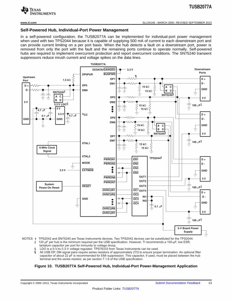
Self-Powered Hub, Individual-Port Power ManagementIn a self-powered configuration, the TUSB2077A can be implemented for individual-port power managementwhen used with two TPS2044 because it is capable of supplying 500 mA of current to each downstream port andcan provide current limiting on a per port basis. When the hub detects a fault on a downstream port, power isremoved from only the port with the fault and the remaining ports continue to operate normally. Self-poweredhubs are required to implement overcurrent protection and report overcurrent conditions. The SN75240 transientsuppressors reduce inrush current and voltage spikes on the data lines.
Figure 10. TUSB2077A Self-Powered Hub, Individual-Port Power-Management Application
Copyright © 2000–2013, Texas Instruments Incorporated Submit Documentation Feedback 13
Product Folder Links: TUSB2077A
6-MHz Clock
Signal
DP1
DM1
DP2
DM2
PWRON1
PWRON7
OVRCUR1
OVRCUR7
GND
XTAL1
XTAL2
EXTMEM
RESET
TPS2044†
IN1EN1
OUT1
D +
D -
5 V
GND
D +
D -
5 V
Downstream
Ports
OC1
TUSB2077A
DP6
DM6
DP7
DM7
SN75240†
A
B
C
D
100 mF
GND
‡
100 mF‡
DP0
DM0
VCC
5 V
3.3 V
GND
D +
D -
Upstream
Port
3.3 V LDO§
SN75240†
A
B5 V
GND
C
D
4.7 mF0.1 mF
4.7 mF
Ferrite Beads
5 V Board Power
Supply
Ferrite Beads
0.1 mF
D +
D -
5 V
GND
D +
D -
5 V
GND
100 mF‡
Ferrite Beads
SN75240†
A
B
C
D
100 mF
BUSPWR
‡
3.3 V
Ferrite Beads
EEDATA/GANGED
System
Power-On Reset
EN2
EN3
EN4
OC2
OC3
OC4
OUT2
OUT3
OUT4
IN2
1.5 kΩ
3.3 V
15 kΩ
15 kΩ
15 kΩ
15 kΩ
15 kΩ
15 kΩ
15 kΩ
15 kΩ
MODE
DP0PUR
¶
NOTES:
LDO is a 5-V-to-3.3-V voltage regulator. TPS76333 from Texas Instruments can be used.All USB DP, DM signal pairs require series resistors of approximately 27
†
¶
TPS2044, TPS2042, and SN75240 are Texas Instruments devices. The TPS2024 can be substituted for the TPS2044.120 µF per hub is the minimum required per the USB specification. However, TI recommends a 100-µF, low ESR,tantalum capacitor per port for immunity to voltage droop.
‡
§Ω to ensure proper termination. An optional filter
capacitor of about 22 pF is recommended for EMI suppression. This capacitor, if used, must be placed between the hubterminal and the series resistor, as per section 7.1.6 of the USB specification.
TUSB2077A
SLLS414E –MARCH 2000–REVISED SEPTEMBER 2013 www.ti.com
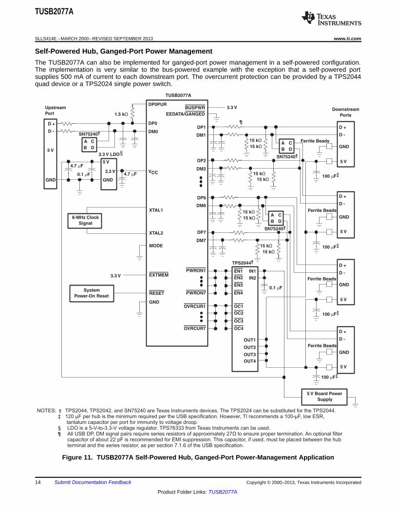
Self-Powered Hub, Ganged-Port Power ManagementThe TUSB2077A can also be implemented for ganged-port power management in a self-powered configuration.The implementation is very similar to the bus-powered example with the exception that a self-powered portsupplies 500 mA of current to each downstream port. The overcurrent protection can be provided by a TPS2044quad device or a TPS2024 single power switch.
Figure 11. TUSB2077A Self-Powered Hub, Ganged-Port Power-Management Application
14 Submit Documentation Feedback Copyright © 2000–2013, Texas Instruments Incorporated
Product Folder Links: TUSB2077A
PACKAGE OPTION ADDENDUM
www.ti.com 6-Sep-2013
Addendum-Page 1
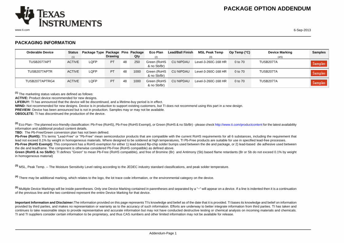
PACKAGING INFORMATION
Orderable Device Status(1)
Package Type PackageDrawing
Pins PackageQty
Eco Plan(2)
Lead/Ball Finish MSL Peak Temp(3)
Op Temp (°C) Device Marking(4/5)
Samples
TUSB2077APT ACTIVE LQFP PT 48 250 Green (RoHS& no Sb/Br)
CU NIPDAU Level-3-260C-168 HR 0 to 70 TUSB2077A
TUSB2077APTR ACTIVE LQFP PT 48 1000 Green (RoHS& no Sb/Br)
CU NIPDAU Level-3-260C-168 HR 0 to 70 TUSB2077A
TUSB2077APTRG4 ACTIVE LQFP PT 48 1000 Green (RoHS& no Sb/Br)
CU NIPDAU Level-3-260C-168 HR 0 to 70 TUSB2077A
(1) The marketing status values are defined as follows:ACTIVE: Product device recommended for new designs.LIFEBUY: TI has announced that the device will be discontinued, and a lifetime-buy period is in effect.NRND: Not recommended for new designs. Device is in production to support existing customers, but TI does not recommend using this part in a new design.PREVIEW: Device has been announced but is not in production. Samples may or may not be available.OBSOLETE: TI has discontinued the production of the device.
(2) Eco Plan - The planned eco-friendly classification: Pb-Free (RoHS), Pb-Free (RoHS Exempt), or Green (RoHS & no Sb/Br) - please check http://www.ti.com/productcontent for the latest availabilityinformation and additional product content details.TBD: The Pb-Free/Green conversion plan has not been defined.Pb-Free (RoHS): TI's terms "Lead-Free" or "Pb-Free" mean semiconductor products that are compatible with the current RoHS requirements for all 6 substances, including the requirement thatlead not exceed 0.1% by weight in homogeneous materials. Where designed to be soldered at high temperatures, TI Pb-Free products are suitable for use in specified lead-free processes.Pb-Free (RoHS Exempt): This component has a RoHS exemption for either 1) lead-based flip-chip solder bumps used between the die and package, or 2) lead-based die adhesive used betweenthe die and leadframe. The component is otherwise considered Pb-Free (RoHS compatible) as defined above.Green (RoHS & no Sb/Br): TI defines "Green" to mean Pb-Free (RoHS compatible), and free of Bromine (Br) and Antimony (Sb) based flame retardants (Br or Sb do not exceed 0.1% by weightin homogeneous material)
(3) MSL, Peak Temp. -- The Moisture Sensitivity Level rating according to the JEDEC industry standard classifications, and peak solder temperature.
(4) There may be additional marking, which relates to the logo, the lot trace code information, or the environmental category on the device.
(5) Multiple Device Markings will be inside parentheses. Only one Device Marking contained in parentheses and separated by a "~" will appear on a device. If a line is indented then it is a continuationof the previous line and the two combined represent the entire Device Marking for that device.
Important Information and Disclaimer:The information provided on this page represents TI's knowledge and belief as of the date that it is provided. TI bases its knowledge and belief on informationprovided by third parties, and makes no representation or warranty as to the accuracy of such information. Efforts are underway to better integrate information from third parties. TI has taken andcontinues to take reasonable steps to provide representative and accurate information but may not have conducted destructive testing or chemical analysis on incoming materials and chemicals.TI and TI suppliers consider certain information to be proprietary, and thus CAS numbers and other limited information may not be available for release.
PACKAGE OPTION ADDENDUM
www.ti.com 6-Sep-2013
Addendum-Page 2
In no event shall TI's liability arising out of such information exceed the total purchase price of the TI part(s) at issue in this document sold by TI to Customer on an annual basis.
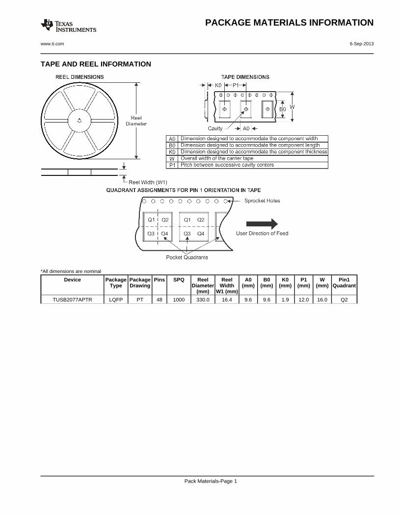
TAPE AND REEL INFORMATION
*All dimensions are nominal
Device PackageType
PackageDrawing
Pins SPQ ReelDiameter
(mm)
ReelWidth
W1 (mm)
A0(mm)
B0(mm)
K0(mm)
P1(mm)
W(mm)
Pin1Quadrant
TUSB2077APTR LQFP PT 48 1000 330.0 16.4 9.6 9.6 1.9 12.0 16.0 Q2
PACKAGE MATERIALS INFORMATION
www.ti.com 6-Sep-2013
Pack Materials-Page 1
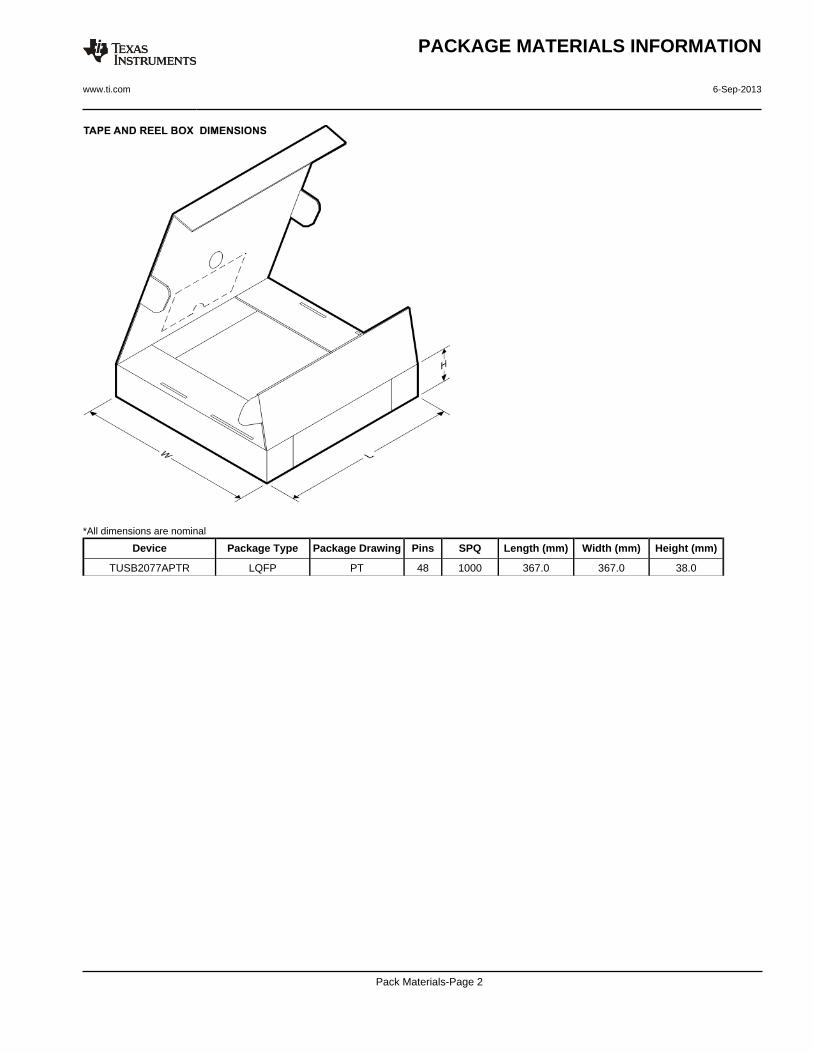
*All dimensions are nominal
Device Package Type Package Drawing Pins SPQ Length (mm) Width (mm) Height (mm)
TUSB2077APTR LQFP PT 48 1000 367.0 367.0 38.0
PACKAGE MATERIALS INFORMATION
www.ti.com 6-Sep-2013
Pack Materials-Page 2
MECHANICAL DATA
MTQF003A – OCTOBER 1994 – REVISED DECEMBER 1996
1POST OFFICE BOX 655303 • DALLAS, TEXAS 75265
PT (S-PQFP-G48) PLASTIC QUAD FLATPACK
4040052/C 11/96
0,13 NOM
0,170,27
25
24
SQ
12
13
36
37
6,807,20
1
48
5,50 TYP
0,25
0,450,75
0,05 MIN
SQ9,208,80
1,351,45
1,60 MAX
Gage Plane
Seating Plane
0,10
0°–7°
0,50 M0,08
NOTES: A. All linear dimensions are in millimeters.B. This drawing is subject to change without notice.C. Falls within JEDEC MS-026D. This may also be a thermally enhanced plastic package with leads conected to the die pads.
IMPORTANT NOTICE
Texas Instruments Incorporated and its subsidiaries (TI) reserve the right to make corrections, enhancements, improvements and otherchanges to its semiconductor products and services per JESD46, latest issue, and to discontinue any product or service per JESD48, latestissue. Buyers should obtain the latest relevant information before placing orders and should verify that such information is current andcomplete. All semiconductor products (also referred to herein as “components”) are sold subject to TI’s terms and conditions of salesupplied at the time of order acknowledgment.
TI warrants performance of its components to the specifications applicable at the time of sale, in accordance with the warranty in TI’s termsand conditions of sale of semiconductor products. Testing and other quality control techniques are used to the extent TI deems necessaryto support this warranty. Except where mandated by applicable law, testing of all parameters of each component is not necessarilyperformed.
TI assumes no liability for applications assistance or the design of Buyers’ products. Buyers are responsible for their products andapplications using TI components. To minimize the risks associated with Buyers’ products and applications, Buyers should provideadequate design and operating safeguards.
TI does not warrant or represent that any license, either express or implied, is granted under any patent right, copyright, mask work right, orother intellectual property right relating to any combination, machine, or process in which TI components or services are used. Informationpublished by TI regarding third-party products or services does not constitute a license to use such products or services or a warranty orendorsement thereof. Use of such information may require a license from a third party under the patents or other intellectual property of thethird party, or a license from TI under the patents or other intellectual property of TI.
Reproduction of significant portions of TI information in TI data books or data sheets is permissible only if reproduction is without alterationand is accompanied by all associated warranties, conditions, limitations, and notices. TI is not responsible or liable for such altereddocumentation. Information of third parties may be subject to additional restrictions.
Resale of TI components or services with statements different from or beyond the parameters stated by TI for that component or servicevoids all express and any implied warranties for the associated TI component or service and is an unfair and deceptive business practice.TI is not responsible or liable for any such statements.
Buyer acknowledges and agrees that it is solely responsible for compliance with all legal, regulatory and safety-related requirementsconcerning its products, and any use of TI components in its applications, notwithstanding any applications-related information or supportthat may be provided by TI. Buyer represents and agrees that it has all the necessary expertise to create and implement safeguards whichanticipate dangerous consequences of failures, monitor failures and their consequences, lessen the likelihood of failures that might causeharm and take appropriate remedial actions. Buyer will fully indemnify TI and its representatives against any damages arising out of the useof any TI components in safety-critical applications.
In some cases, TI components may be promoted specifically to facilitate safety-related applications. With such components, TI’s goal is tohelp enable customers to design and create their own end-product solutions that meet applicable functional safety standards andrequirements. Nonetheless, such components are subject to these terms.
No TI components are authorized for use in FDA Class III (or similar life-critical medical equipment) unless authorized officers of the partieshave executed a special agreement specifically governing such use.
Only those TI components which TI has specifically designated as military grade or “enhanced plastic” are designed and intended for use inmilitary/aerospace applications or environments. Buyer acknowledges and agrees that any military or aerospace use of TI componentswhich have not been so designated is solely at the Buyer's risk, and that Buyer is solely responsible for compliance with all legal andregulatory requirements in connection with such use.
TI has specifically designated certain components as meeting ISO/TS16949 requirements, mainly for automotive use. In any case of use ofnon-designated products, TI will not be responsible for any failure to meet ISO/TS16949.
Products Applications
Audio www.ti.com/audio Automotive and Transportation www.ti.com/automotive
Amplifiers amplifier.ti.com Communications and Telecom www.ti.com/communications
Data Converters dataconverter.ti.com Computers and Peripherals www.ti.com/computers
DLP® Products www.dlp.com Consumer Electronics www.ti.com/consumer-apps
DSP dsp.ti.com Energy and Lighting www.ti.com/energy
Clocks and Timers www.ti.com/clocks Industrial www.ti.com/industrial
Interface interface.ti.com Medical www.ti.com/medical
Logic logic.ti.com Security www.ti.com/security
Power Mgmt power.ti.com Space, Avionics and Defense www.ti.com/space-avionics-defense
Microcontrollers microcontroller.ti.com Video and Imaging www.ti.com/video
RFID www.ti-rfid.com
OMAP Applications Processors www.ti.com/omap TI E2E Community e2e.ti.com
Wireless Connectivity www.ti.com/wirelessconnectivity
Mailing Address: Texas Instruments, Post Office Box 655303, Dallas, Texas 75265Copyright © 2013, Texas Instruments Incorporated