IEEE JOURNAL OF SELECTED TOPICS IN QUANTUM ELECTRONICS, VOL. 18, NO. 3, MAY/JUNE 2012 1223 Toward Spectral-Domain Optical Coherence Tomography on a Chip B. Imran Akca, Van Duc Nguyen, Jeroen Kalkman, Nur Ismail, Gabriel Sengo, Fei Sun, Alfred Driessen, Ton G. van Leeuwen, Markus Pollnau, Kerstin W¨ orhoff, and Ren´ e M. de Ridder, Member, IEEE Abstract—We present experimental results of a spectral-domain optical coherence tomography system based on an integrated optical spectrometer. A 195-channel arrayed-waveguide-grating (AWG) spectrometer with 0.4-nm channel spacing centered at 1300nm and a 125-channel AWG with 0.16-nm channel spacing centered at 800 nm have been fabricated in silicon oxynitride wave- guide technology. Interferometric distance measurements have been performed by launching light from a broadband source into a free-space Michelson interferometer, with its output coupled into the AWG. A maximum imaging depth of 1 mm and axial resolution of 25 and 20 μm in air are demonstrated for the 800- and 1300-nm ranges, respectively. Index Terms—Arrayed waveguide grating (AWG), optical co- herence tomography (OCT), optical waveguides, silicon oxynitride (SiON), spectrometer. I. INTRODUCTION O PTICAL coherence tomography (OCT) [1] is a noninva- sive optical technique for high-resolution cross-sectional imaging of biological tissue, with many applications in clinical medicine. The measurement principle of OCT is based on low- coherence interferometry (LCI) in which interference patterns due to the superposition of a multitude of waves with a large spread in wavelengths are studied. These distinctive patterns enable one to determine the location at which light is reflected Manuscript received May 14, 2011; revised September 13, 2011 and October 4, 2011; accepted October 5, 2011. Date of publication October 13, 2011; date of current version June 1, 2012. This work was supported by the Smart Mix Program of the Netherlands Ministry of Economic Affairs and the Netherlands Ministry of Education, Culture and Science, and by the Dutch Senter-Novem Merging Electronics and Micro and Nano Photonics in Integrated Systems Project. B. I. Akca, N. Ismail, G. Sengo, A. Driessen, M. Pollnau, K. W¨ orhoff, and R. M. de Ridder are with the Integrated Optical MicroSystems Group, MESA+ Institute for Nanotechnology, University of Twente, 7500 AE Enschede, The Netherlands (e-mail: [email protected]; N.Ismail@ utwente.nl; [email protected]; [email protected]; M.Pollnau@ utwente.nl; [email protected]; [email protected]). V. Duc Nguyen and J. Kalkman are with the Department of Biomedical En- gineering and Physics, Academic Medical Center, University of Amsterdam, NL-1100 DE Amsterdam, The Netherlands (e-mail: [email protected]; [email protected]). F. Sun is with the Institute of Microelectronics, A ∗ STAR, 117685, Singapore (e-mail: [email protected]). T. G. van Leeuwen is with the Biomedical Photonic Imaging Group, MIRA Institute for Biomedical Technology and Technical Medicine, University of Twente, 7500 AE Enschede, The Netherlands, and also with the Depart- ment of Biomedical Engineering and Physics, Academic Medical Center, Uni- versity of Amsterdam, NL-1100 DE Amsterdam, The Netherlands (e-mail: [email protected]). Color versions of one or more of the figures in this paper are available online at http://ieeexplore.ieee.org. Digital Object Identifier 10.1109/JSTQE.2011.2171674 back and to measure the depth profile of the scattering ampli- tude. By performing multiple LCI measurements at different lateral coordinates on a sample, a 3-D cross-sectional image of the scattering amplitude can be constructed. Current state-of-the-art OCT systems operate in the Fourier domain, using either a broadband light source and a spec- trometer, known as “spectral-domain OCT” (SD-OCT), or a rapidly tunable laser, known as “swept-source OCT” (SS-OCT). Fourier-domain OCT (FD-OCT) systems (SS-OCT and SD- OCT) were invented by Fercher et al. in 1995 [2]. However, FD-OCT gained wide acceptance only after nearly ten years, when it was realized that FD-OCT offered a significant sensi- tivity advantage over time-domain OCT. SS-OCT systems are advantageous for their simple single-element detection and bet- ter sensitivity with imaging depth (lower sensitivity roll-off), but they typically have lower axial resolution compared to SD- OCT and suffer from phase instability. In addition, they require a more expensive light source. SD-OCT systems can utilize sim- ple broadband sources; however, they suffer from severe signal roll-off in depth and require more complicated detection optics, i.e., line scan cameras and spectrometers [3]. Ultrahigh axial resolution of 2.1–3.5 μm in the retina from 10 to 29 kHz axial scan rates were demonstrated with SD-OCT systems [4]–[6]. Recently, by using high-speed CMOS cameras in retinal imag- ing, an axial scan rate of 312 kHz was obtained with an axial resolution of 8–9 μm in the 850-nm spectral range [7]. Current commercial SD-OCT systems typically achieve ∼5 μm axial resolution with ∼25–27 kHz axial scan rates over an imaging range of ∼2.0–2.6 mm. The fastest speed in retina imaging was demonstrated by Fujimoto et al. at 100 000–400 000 axial scans per second with an axial resolution of 5.3 μm, using a 1050-nm SS-OCT system [8]. Although current SS-OCT systems seem to perform better than SD-OCT systems due to the improved light sources, SD-OCT systems have been used quite extensively for polarization sensitive OCT, Doppler OCT, ultrawide-bandwidth OCT, ultrahigh-resolution OCT and, moreover, they represent the state of the art in commercial ophthalmologic OCT sys- tems [3]. Both systems contain a multitude of fiber and free- space optical components that make these instruments costly and bulky. The size and cost of an OCT system can be de- creased significantly by the use of integrated optics. A suitable material technology and optimum design may allow one to fabri- cate extremely compact and low-cost OCT systems. In addition, integrated optics can enhance the performance of OCT by, for example, parallelization [9], [10] of OCT devices on a chip. Only limited data on the implementation of OCT components on a chip exists. Culemann et al. [11] fabricated an integrated optical sensor chip in ion-exchanged low-index-contrast glass 1077-260X/$26.00 © 2011 IEEE

Welcome message from author
This document is posted to help you gain knowledge. Please leave a comment to let me know what you think about it! Share it to your friends and learn new things together.
Transcript
IEEE JOURNAL OF SELECTED TOPICS IN QUANTUM ELECTRONICS, VOL. 18, NO. 3, MAY/JUNE 2012 1223
Toward Spectral-Domain Optical CoherenceTomography on a Chip
B. Imran Akca, Van Duc Nguyen, Jeroen Kalkman, Nur Ismail, Gabriel Sengo, Fei Sun, Alfred Driessen,Ton G. van Leeuwen, Markus Pollnau, Kerstin Worhoff, and Rene M. de Ridder, Member, IEEE
Abstract—We present experimental results of a spectral-domainoptical coherence tomography system based on an integratedoptical spectrometer. A 195-channel arrayed-waveguide-grating(AWG) spectrometer with 0.4-nm channel spacing centered at1300 nm and a 125-channel AWG with 0.16-nm channel spacingcentered at 800 nm have been fabricated in silicon oxynitride wave-guide technology. Interferometric distance measurements havebeen performed by launching light from a broadband source intoa free-space Michelson interferometer, with its output coupled intothe AWG. A maximum imaging depth of 1 mm and axial resolutionof 25 and 20 μm in air are demonstrated for the 800- and 1300-nmranges, respectively.
Index Terms—Arrayed waveguide grating (AWG), optical co-herence tomography (OCT), optical waveguides, silicon oxynitride(SiON), spectrometer.
I. INTRODUCTION
O PTICAL coherence tomography (OCT) [1] is a noninva-sive optical technique for high-resolution cross-sectional
imaging of biological tissue, with many applications in clinicalmedicine. The measurement principle of OCT is based on low-coherence interferometry (LCI) in which interference patternsdue to the superposition of a multitude of waves with a largespread in wavelengths are studied. These distinctive patternsenable one to determine the location at which light is reflected
Manuscript received May 14, 2011; revised September 13, 2011 and October4, 2011; accepted October 5, 2011. Date of publication October 13, 2011; dateof current version June 1, 2012. This work was supported by the Smart MixProgram of the Netherlands Ministry of Economic Affairs and the NetherlandsMinistry of Education, Culture and Science, and by the Dutch Senter-NovemMerging Electronics and Micro and Nano Photonics in Integrated SystemsProject.
B. I. Akca, N. Ismail, G. Sengo, A. Driessen, M. Pollnau, K. Worhoff,and R. M. de Ridder are with the Integrated Optical MicroSystems Group,MESA+ Institute for Nanotechnology, University of Twente, 7500 AEEnschede, The Netherlands (e-mail: [email protected]; [email protected]; [email protected]; [email protected]; [email protected]; [email protected]; [email protected]).
V. Duc Nguyen and J. Kalkman are with the Department of Biomedical En-gineering and Physics, Academic Medical Center, University of Amsterdam,NL-1100 DE Amsterdam, The Netherlands (e-mail: [email protected];[email protected]).
F. Sun is with the Institute of Microelectronics, A∗STAR, 117685, Singapore(e-mail: [email protected]).
T. G. van Leeuwen is with the Biomedical Photonic Imaging Group, MIRAInstitute for Biomedical Technology and Technical Medicine, University ofTwente, 7500 AE Enschede, The Netherlands, and also with the Depart-ment of Biomedical Engineering and Physics, Academic Medical Center, Uni-versity of Amsterdam, NL-1100 DE Amsterdam, The Netherlands (e-mail:[email protected]).
Color versions of one or more of the figures in this paper are available onlineat http://ieeexplore.ieee.org.
Digital Object Identifier 10.1109/JSTQE.2011.2171674
back and to measure the depth profile of the scattering ampli-tude. By performing multiple LCI measurements at differentlateral coordinates on a sample, a 3-D cross-sectional image ofthe scattering amplitude can be constructed.
Current state-of-the-art OCT systems operate in the Fourierdomain, using either a broadband light source and a spec-trometer, known as “spectral-domain OCT” (SD-OCT), or arapidly tunable laser, known as “swept-source OCT” (SS-OCT).Fourier-domain OCT (FD-OCT) systems (SS-OCT and SD-OCT) were invented by Fercher et al. in 1995 [2]. However,FD-OCT gained wide acceptance only after nearly ten years,when it was realized that FD-OCT offered a significant sensi-tivity advantage over time-domain OCT. SS-OCT systems areadvantageous for their simple single-element detection and bet-ter sensitivity with imaging depth (lower sensitivity roll-off),but they typically have lower axial resolution compared to SD-OCT and suffer from phase instability. In addition, they requirea more expensive light source. SD-OCT systems can utilize sim-ple broadband sources; however, they suffer from severe signalroll-off in depth and require more complicated detection optics,i.e., line scan cameras and spectrometers [3]. Ultrahigh axialresolution of 2.1–3.5 μm in the retina from 10 to 29 kHz axialscan rates were demonstrated with SD-OCT systems [4]–[6].Recently, by using high-speed CMOS cameras in retinal imag-ing, an axial scan rate of 312 kHz was obtained with an axialresolution of 8–9 μm in the 850-nm spectral range [7]. Currentcommercial SD-OCT systems typically achieve ∼5 μm axialresolution with ∼25–27 kHz axial scan rates over an imagingrange of ∼2.0–2.6 mm. The fastest speed in retina imaging wasdemonstrated by Fujimoto et al. at 100 000–400 000 axial scansper second with an axial resolution of 5.3 μm, using a 1050-nmSS-OCT system [8]. Although current SS-OCT systems seem toperform better than SD-OCT systems due to the improved lightsources, SD-OCT systems have been used quite extensively forpolarization sensitive OCT, Doppler OCT, ultrawide-bandwidthOCT, ultrahigh-resolution OCT and, moreover, they representthe state of the art in commercial ophthalmologic OCT sys-tems [3]. Both systems contain a multitude of fiber and free-space optical components that make these instruments costlyand bulky. The size and cost of an OCT system can be de-creased significantly by the use of integrated optics. A suitablematerial technology and optimum design may allow one to fabri-cate extremely compact and low-cost OCT systems. In addition,integrated optics can enhance the performance of OCT by, forexample, parallelization [9], [10] of OCT devices on a chip.
Only limited data on the implementation of OCT componentson a chip exists. Culemann et al. [11] fabricated an integratedoptical sensor chip in ion-exchanged low-index-contrast glass
1077-260X/$26.00 © 2011 IEEE
1224 IEEE JOURNAL OF SELECTED TOPICS IN QUANTUM ELECTRONICS, VOL. 18, NO. 3, MAY/JUNE 2012
for time-domain OCT, with all other components external to theoptical chip. Margallo-Balbas et al. realized a rapidly scanningdelay line in silicon—based on the thermo-optic (TO) effect ofsilicon—for application in time-domain OCT, operating at linerates of 10 kHz and a scan range of nearly 1 mm [12]. Yurtseveret al. [13] demonstrated a silicon-based Michelson interferom-eter (MI) for a SS-OCT system with 40 μm of axial resolu-tion and a sensitivity of 25 dB, both insufficient for imaging.Nguyen et al. [14] demonstrated integrated elliptic couplers andapplied them to Fizeau-based spectral-domain low-coherencedepth ranging. Choi et al. were the first to demonstrate the per-formance of an arrayed-waveguide-grating (AWG) spectrome-ter in an SD-OCT system with a depth range of 3 mm and anaxial resolution of 23 μm. However, they needed semiconduc-tor optical amplifiers in order to obtain sufficient sensitivity forimaging [15]. Recently, we have demonstrated a depth range of1 mm and an axial resolution of 19 μm by performing interfero-metric distance measurements in a fiber-based SD-OCT systemwith a silicon-oxynitride (SiON)-based AWG designed for the1300-nm wavelength range [16].
One of the key components of an SD-OCT system is thehigh-resolution spectrometer (spectrometers also have been em-ployed in SS-OCT to reduce motion artifacts [17]). Althoughintegration of a spectrometer on a chip is challenging, AWGspresent a well established way toward miniaturization. AWGsare used for wavelength (de)multiplexing in telecommunication,offering high resolution over a small bandwidth [18]. AWGs areideally suited for applications such as OCT and spectroscopy,with their high spectral resolution, small form factor, large band-width, and low insertion loss [19]. In addition to their advan-tages listed previously, AWGs are cost effective, which makesthem favorable for integration with SD-OCT systems. How-ever, there are design limitations on resolution and free spectralrange (FSR), which restrict the axial resolution and maximumimaging range of SD-OCT systems. By applying different ap-proaches (e.g., cascading several AWGs and compensating theinherent additional loss by increasing the power of the lightsource), these limitations can be overcome.
SiON is a promising material for AWG spectrometer appli-cations. Its refractive index can be chosen between the valuesof silicon dioxide (1.45) and silicon nitride (2.0), thus, allowingfor a flexible waveguide design [20]. A small bending radiusdown to several micrometers can be obtained by using the high-est refractive index contrast with a proper waveguide geometry.Furthermore, SiON is transparent in a broad wavelength rangefrom 210 nm to beyond 2000 nm [21], so that AWGs can befabricated for both the visible and infrared wavelength rangesby use of the same material system; in specific cases, even thesame AWG structure could be used for both regions. In the liter-ature, there is only limited data on SiON-based AWG spectrom-eters [22]–[27]. Schauwecker et al. reported the smallest AWGon the SiON platform, with an overall chip size of 5 mm ×2 mm [22]. The fiber-to-chip coupling loss of a 32-channel,100-GHz spacing AWG has been reduced significantly with in-tegrated spot-size converters [23]. The largest FSR was reportedby Shimoda et al. [24]. Their AWG showed 2-nm channel spac-ing, 80-nm FSR, and 2.2-dB insertion loss.
In this paper, we present two SiON-based AWG spectrometersfor the spectral ranges near 800 and 1300 nm, which are aimedto be used as integrated spectrometers in future fully integratedSD-OCT systems. We investigate the performance of integratedSiON-based AWG spectrometers with high resolution and largeFSR in interferometric depth ranging and OCT imaging, therebydemonstrating the first important step toward miniaturization ofan SD-OCT system.
II. DESIGN AND REALIZATION
A. Essential OCT Parameters
The essential parameters that determine the imaging qualityof FD-OCT systems are center wavelength, axial resolution,maximum imaging depth, signal-to-noise ratio (SNR), and sen-sitivity roll-off in depth.
First, the OCT imaging depth is limited by the amount ofscattering (higher at shorter wavelengths) and absorption (higherat longer wavelengths) in biological tissue. Therefore, the OCTimaging depth depends on the choice of center wavelength ofthe OCT system. In this paper, two common OCT wavelengths(λc ) are used, 800 nm for imaging ophthalmic structures wherewater absorption is dominant and 1300 nm for dermal imagingwhere scattering is dominant.
Second, the axial resolution of an SD-OCT system is deter-mined by the effective bandwidth of the light that is detected. Itdepends on both the bandwidth of the light source and the band-width of the spectrometer. If the spectrum of the light source,as measured with the spectrometer, has a Gaussian envelopewith full-width at half-maximum (FWHM) ΔλFWHM , the axial(depth) resolution Δz is given by [28]
Δz =2 ln 2πn
(λ2
c
ΔλFWHM
)(1)
where n is the (group) refractive index of the imaged tissue.Third, the maximum imaging depth zmax in SD-OCT is de-
termined by the spectral sampling interval (δk, k is the wavenumber). From Nyquists’s sampling theorem, the spectral sam-pling at δk spacing leads to a maximum path length of 1/(2δk).However, since every path length corresponds to half the depth(light travels back and forth to the detector), the imaging depthbecomes 1/(4δk). Considering the wavenumber-to-wavelengthconversion, it becomes [29]
zmax =λ2
c
4nδλ(2)
where δλ is the wavelength resolution of the spectrometer.Fourth, the roll-off in depth of the SD-OCT signal is de-
termined by the spectral content of the spectrometer and thecamera pixel size. The imaging range of SD-OCT is limited bythe signal roll-off, which is the attenuation of the OCT signal dueto washout of the interference fringe visibility with increasingdepth. The signal amplitude roll-off function is given by [30]
A(z) =sin(dxRz)(dxRz)
exp[−a2R2z2
4 ln 2
](3)
AKCA et al.: TOWARD SPECTRAL-DOMAIN OPTICAL COHERENCE TOMOGRAPHY ON A CHIP 1225
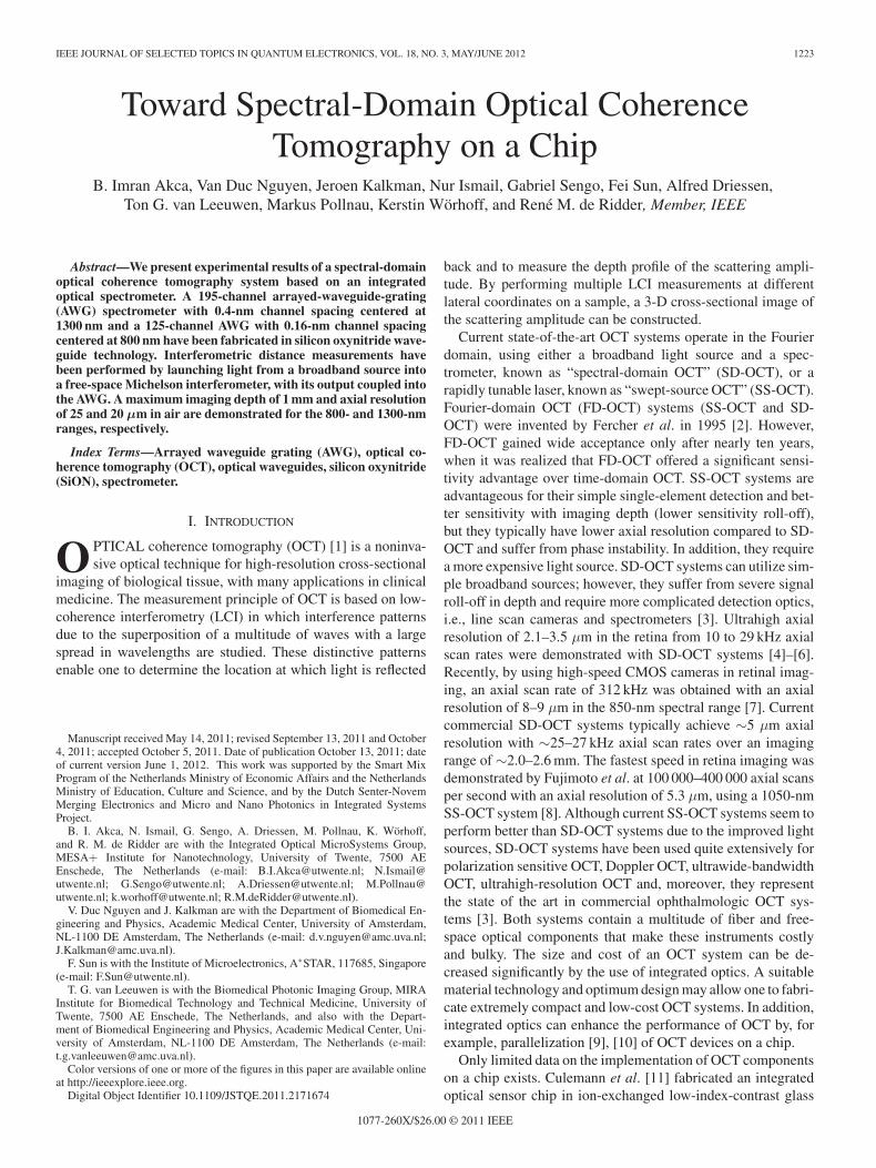
Fig. 1. (a) Schematic layout of an AWG. Channel waveguide geometry for(b) the AWG centered at 800 nm and (c) the AWG centered at 1300 nm.
where dx is the pixel width, R is the reciprocal linear dispersionof the spectrometer (δk/dx ), and a is the spot size. The Sinc andGaussian functions in (3) correspond to the Fourier transformof the square-shaped camera pixels and Gaussian beam profilein the spectrometer, respectively. By applying wavenumber-to-wavelength conversion, (3) becomes
A(z) =sin
((2πδλ/λ2)z
)(2πδλ/λ2)z
exp
[− π2
ln 2
(aδλz
λ2dx
)2]
. (4)
Rearranging (4) by using (2) yields
A(z) =sin(πz/2zmax)(πz/2zmax)
exp
[− π2
16 ln 2
(a
dx
)2 (z
zmax
)2]
.
(5)zmax is taken from (2) and (a/dx ) is defined as ω in [31], whichis the ratio of the spectrometer FWHM spectral resolution to thewavelength resolution.
Finally, for maximum SNR, the spectrometer loss should beminimized in the design stage. Typical SNR values for high-quality OCT imaging are on the order of 100 dB [3], [4], [30].
B. AWG Operation
The operation of an AWG [18] is briefly explained, refer-ring to Fig. 1(a). Light from an input waveguide diverges in afirst free propagation region (FPR) in order to illuminate theinput facets of an array of waveguides with a linearly increas-ing length. For a central wavelength λc , the phase differenceat the output facets of adjacent array waveguides is an integermultiple of 2π. Since these facets are arranged on a circle, acylindrical wavefront is formed at the beginning of a secondFPR, which generates a focal spot at the central output channel.Since the phase shift caused by the length differences betweenarrayed waveguides is linearly dependent on wavelength, theresulting wavelength-dependent phase gradient implies a tilt ofthe cylindrical wavefront at the beginning of the second FPR,which causes the focal spot to shift with wavelength to differentoutput waveguides.
C. AWG Parameters for OCT Imaging
The axial resolution of an SD-OCT system using an AWGis determined by the effective bandwidth of the detected spec-trum, which depends on both the bandwidth of the light sourceand the FSR of the spectrometer. Matching the bandwidth ofthe AWG transmission function with the bandwidth of the lightsource is the most economical configuration, since for a givensource bandwidth, the axial resolution will not improve if thebandwidth of the AWG transmission function is made muchlarger than this bandwidth, and vice versa. The maximum valueof the transmission bandwidth of an AWG is its FSR, whichis valid for loss uniformity ≤−3 dB. In practice, the FSR ofan AWG is limited by the size of the device. In this paper, theFSR values of our AWG spectrometers are chosen to be 20 and78 nm for λc = 800 and 1300 nm, respectively, by consideringthe design limitations. The bandwidths of the light sources thatwe used in the OCT measurements are much smaller than thebandwidths of the AWG spectrometers: ΔλFWHM = 13 and40 nm, respectively. In this way, the axial resolution is mainlydetermined by the bandwidth of the light source. Accordingto (1), the bandwidths of the chosen light sources limit thetheoretical axial resolution (for air, n = 1) to Δz = 23 and18.5 μm for λc = 800 and 1300 nm, respectively. In tissue (n∼ 1.33), the aforementioned axial resolutions become 17 and14 μm, respectively. With a proper light source (larger band-width) and an AWG with a larger FSR (smaller grating order),the current axial resolution values can be improved to the levelof existing OCT systems.
For both spectral ranges, we aim at a maximum depth rangeof zmax = 1 mm, which according to (2) requires a wavelengthspacing of δλ = 0.16 and 0.4 nm for the 800- and 1300-nmAWG, respectively. The choice for 1-mm imaging depth is acompromise between various imaging performance parameters.Given a fixed size of the AWG imaging plane, a larger imagingdepth can be obtained when using an AWG with higher resolu-tion; however, this would result in a lower optical bandwidth andlower spatial OCT resolution. Smaller spacing between adjacentwaveguides results in an increased crosstalk and, consequently,more signal roll-off in depth.
For an SD-OCT system with an AWG spectrometer, the roll-off in depth is determined by the spectral content of the AWGoutput channels. Due to dispersion in the second FPR, the spec-tral content is limited by the size of the output waveguides.However, the spectral content in a single output waveguide canbe increased due to diffraction-limited focusing of the light ontothe output channel, crosstalk between output waveguides, andfabrication imperfections. For an AWG-based SD-OCT system,light is sampled twice; first at the focal plane of the AWG due todiscretely located output waveguides and second at the camerapixels. The first sampling due to AWG output channels addsan extra Sinc term to (5), which is the Fourier transform of therectangular-shaped output waveguides. In the extra Sinc term,caused by the AWG sampling, dx is the tapered output wave-guide width wo and the reciprocal linear dispersion is defined asδk/do , where do is the spacing between adjacent output waveg-uides. By inserting the AWG parameters into the Sinc term of
1226 IEEE JOURNAL OF SELECTED TOPICS IN QUANTUM ELECTRONICS, VOL. 18, NO. 3, MAY/JUNE 2012
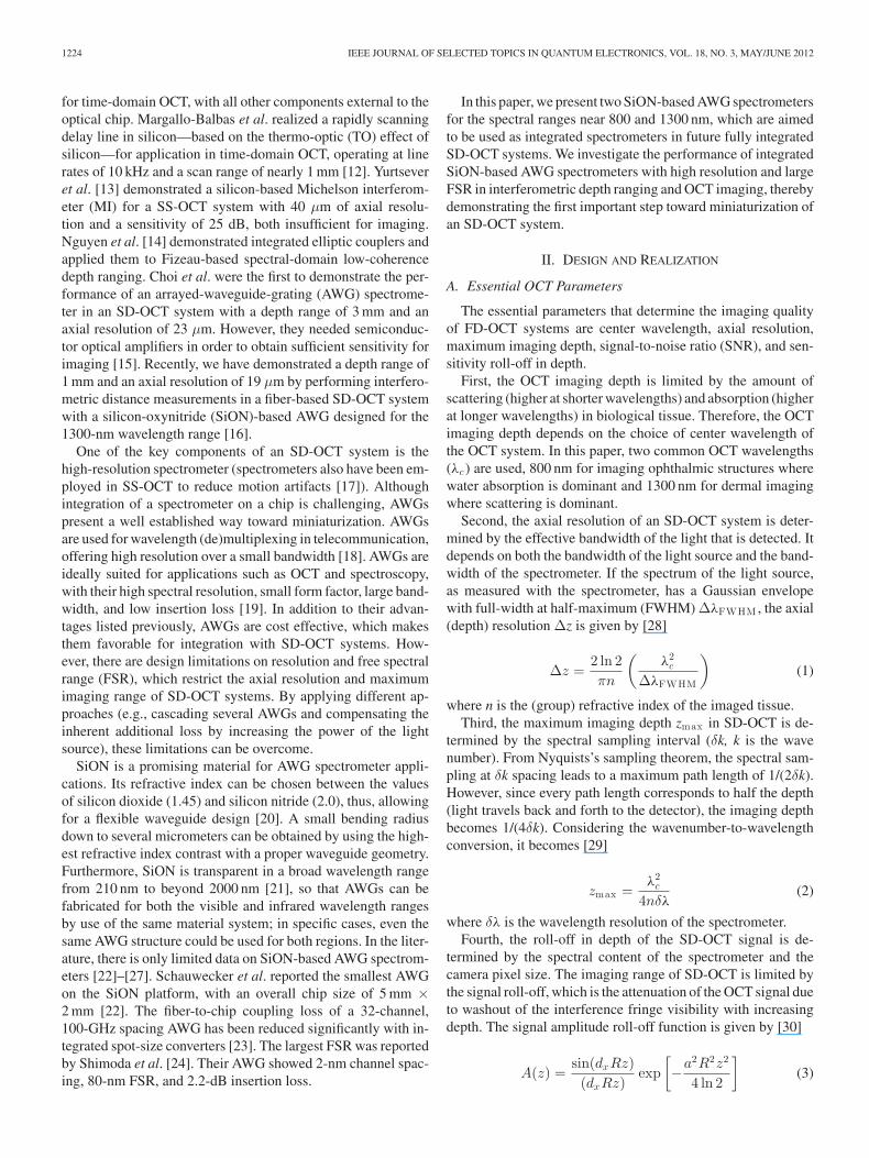
Fig. 2. (a) Geometry of the receiver side of the AWG (second FPR) anddefinition of parameters wa , da , wo , do , and R (see Table I). (b) Adjacentcrosstalk and excess loss versus output taper width wo .
(3) and following the same conversions, the final formula of theextra Sinc term becomes
sin(wo/do)(πz/2zmax)(wo/do)(πz/2zmax)
. (6)
By inserting (6) into (5), the modified formula of sensitivityroll-off is obtained
A(z) =[sin(kπz/2zmax)(kπz/2zmax)
] [sin(πz/2zmax)(πz/2zmax)
]
× exp
[− π2ω2
16 ln 2
(z
zmax
)2]
(7)
where k = wo /do is the ratio of the width of the output waveguideto the separation between them at the focal plane of the AWG[see Fig. 2(a)]. Both AWG spectrometers are designed withk = 0.5. In order to avoid severe signal roll-off in depth, ω ischosen smaller than 1, which necessitates an adjacent-channelcrosstalk value of less than −10 dB. The desired crosstalk valueis achieved by setting the spacing between the output waveg-uides in the focal plane of the AWG spectrometers accordingly.The expected lower limit of ω is calculated with the simulatedFWHM spectral resolution of the spectrometer and results inω = 0.32 and 0.55 for the 800- and 1300-nm AWG,respectively.
For maximum SNR, the AWG spectrometer loss is mini-mized by applying linear tapers at the interfaces of arrayedand input/output waveguides with the FPRs, as demonstratedin Fig. 2(a). Ideally, the gaps near the FPR between arrayedwaveguides should approach zero in order to capture more lightand, thereby, reduce the excess loss. This would, however, resultin extremely sharp features that cannot be accurately reproducedby our lithographic processes; therefore, the gap width was cho-sen to be 1 μm for the arrayed waveguides. The taper width ofthe input/output waveguides was determined as a compromisebetween loss and adjacent-channel crosstalk: the larger the taperwidth, the lower the excess loss and the higher the crosstalk, asshown in Fig. 2(b), which is the simulation result of a typicalAWG spectrometer.
As crosstalk arises from evanescent coupling between out-put waveguides, it decreases with increasing spacing. How-ever, this leads to increased device size and, therefore, needs to
TABLE IDESIGN PARAMETERS OF THE AWG SPECTROMETERS
be carefully designed. Acceptable minimum spacings betweenthe arrayed waveguides and between the output waveguideswere found by simulating device behavior using the 2-D beampropagation method in order to have an excess loss value of≤3 dB (for the central channels) and a crosstalk value of ≤−20dB. The simulation results of both devices confirm that ourchoice of taper width and waveguide spacing fulfills the afore-mentioned excess loss and crosstalk requirements (see Table II).
D. AWG Design and Simulations
For both spectrometers, single-mode SiON channelwaveguides, with the parameters provided in Table I, were fab-ricated. As SiON is transparent over a broad wavelength rangethat covers all the frequently used OCT wavelength bands at800, 1000, and 1300 nm, AWGs can be fabricated for all thesewavelength ranges in the same material system. The size of eachdevice is optimized by beam-propagation simulations, which re-sulted in chip areas of 2.6 cm × 2.1 cm and 3 cm × 2.5 cm forthe 800- and 1300-nm AWG, respectively.
The given refractive index values of core and cladding lay-ers are for TE polarization. For maximum compactness of thedevices, the refractive index of the core layer was chosen ashigh as possible, as consistent with the single-mode conditionand limitations of the fabrication process. Schematic represen-tations of the channel waveguides at 800 and 1300 nm are shownin Fig. 1(b) and (c), respectively.
For the 800-nm AWG, at the central channels, a crosstalk of−35 dB and an excess loss (with respect to a curved waveguide)of 2.6 dB were calculated. At the outermost channels, these val-ues are −27 and 5.35 dB, respectively. The 3-dB bandwidth wascalculated as 0.052 nm. For the 1300-nm AWG, crosstalk valuesof −33 and −20 dB and excess loss values of 1.8 and 6.3 dBwere simulated for the central and outermost channels, respec-tively. The 3-dB bandwidth was calculated as 0.22 nm. Using atypical material birefringence of 1.5 × 10⁻³ , the polarization-dependent wavelength shift was calculated with a 2-D beam
AKCA et al.: TOWARD SPECTRAL-DOMAIN OPTICAL COHERENCE TOMOGRAPHY ON A CHIP 1227
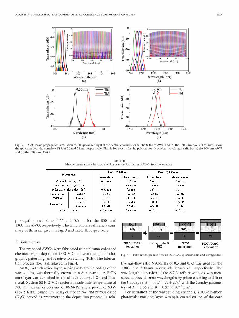
Fig. 3. AWG beam propagation simulation for TE-polarized light at the central channels for (a) the 800-nm AWG and (b) the 1300-nm AWG. The insets showthe spectrum over the complete FSR of 20 and 78 nm, respectively. Simulation results for the polarization-dependent wavelength shift for (c) the 800-nm AWGand (d) the 1300-nm AWG.
TABLE IIMEASUREMENT AND SIMULATION RESULTS OF FABRICATED AWG SPECTROMETERS
propagation method as 0.55 and 0.6 nm for the 800- and1300-nm AWG, respectively. The simulation results and a sum-mary of them are given in Fig. 3 and Table II, respectively.
E. Fabrication
The proposed AWGs were fabricated using plasma-enhancedchemical vapor deposition (PECVD), conventional photolitho-graphic patterning, and reactive ion etching (RIE). The fabrica-tion process flow is displayed in Fig. 4.
An 8-μm-thick oxide layer, serving as bottom cladding of thewaveguides, was thermally grown on a Si substrate. A SiONcore layer was deposited in a load-lock-equipped Oxford Plas-malab System 80 PECVD reactor at a substrate temperature of300 ◦C, a chamber pressure of 86.66 Pa, and a power of 60 W(187.5 KHz). Silane (2% SiH4 diluted in N2) and nitrous oxide(N2O) served as precursors in the deposition process. A rela-
Fig. 4. Fabrication process flow of the AWG spectrometers and waveguides.
tive gas-flow ratio N2O/SiH4 of 0.3 and 0.73 was used for the1300- and 800-nm waveguide structures, respectively. Thewavelength dispersion of the SiON refractive index was mea-sured at three discrete wavelengths by prism coupling and fit tothe Cauchy relation n(λ) = A + B/λ2 with the Cauchy parame-ters of A = 1.55 and B = 6.93 × 10⁻³ μm2 .
For definition of the waveguiding channels, a 500-nm-thickphotoresist masking layer was spin-coated on top of the core
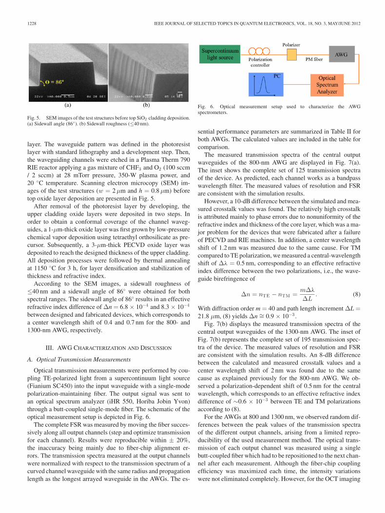
1228 IEEE JOURNAL OF SELECTED TOPICS IN QUANTUM ELECTRONICS, VOL. 18, NO. 3, MAY/JUNE 2012
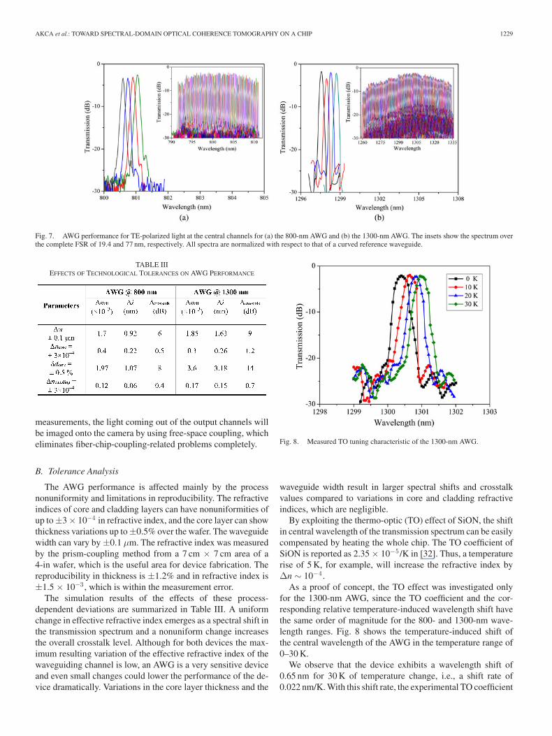
Fig. 5. SEM images of the test structures before top SiO2 cladding deposition.(a) Sidewall angle (86◦). (b) Sidewall roughness (≤40 nm).
layer. The waveguide pattern was defined in the photoresistlayer with standard lithography and a development step. Then,the waveguiding channels were etched in a Plasma Therm 790RIE reactor applying a gas mixture of CHF3 and O2 (100 sccm/ 2 sccm) at 28 mTorr pressure, 350-W plasma power, and20 ◦C temperature. Scanning electron microcopy (SEM) im-ages of the test structures (w = 2 μm and h = 0.8 μm) beforetop oxide layer deposition are presented in Fig. 5.
After removal of the photoresist layer by developing, theupper cladding oxide layers were deposited in two steps. Inorder to obtain a conformal coverage of the channel waveg-uides, a 1-μm-thick oxide layer was first grown by low-pressurechemical vapor deposition using tetraethyl orthosilicate as pre-cursor. Subsequently, a 3-μm-thick PECVD oxide layer wasdeposited to reach the designed thickness of the upper cladding.All deposition processes were followed by thermal annealingat 1150 ◦C for 3 h, for layer densification and stabilization ofthickness and refractive index.
According to the SEM images, a sidewall roughness of≤40 nm and a sidewall angle of 86◦ were obtained for bothspectral ranges. The sidewall angle of 86◦ results in an effectiverefractive index difference of Δn = 6.8 × 10⁻⁴ and 8.3 × 10⁻⁴
between designed and fabricated devices, which corresponds toa center wavelength shift of 0.4 and 0.7 nm for the 800- and1300-nm AWG, respectively.
III. AWG CHARACTERIZATION AND DISCUSSION
A. Optical Transmission Measurements
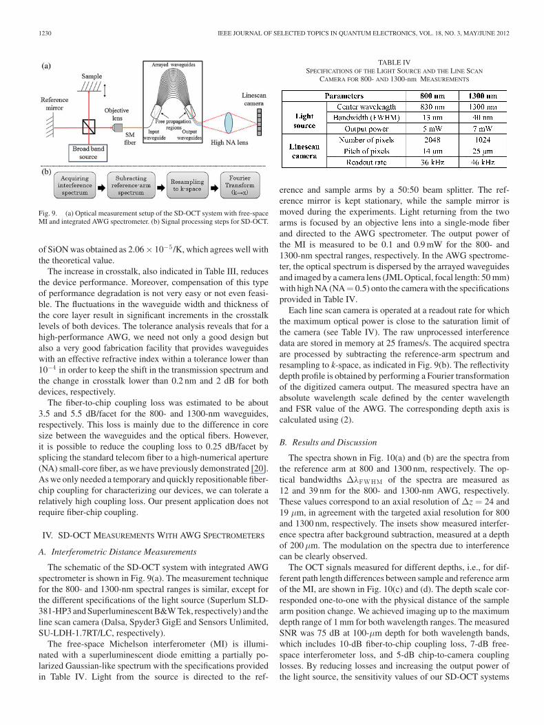
Optical transmission measurements were performed by cou-pling TE-polarized light from a supercontinuum light source(Fianium SC450) into the input waveguide with a single-modepolarization-maintaining fiber. The output signal was sent toan optical spectrum analyzer (iHR 550, Horiba Jobin Yvon)through a butt-coupled single-mode fiber. The schematic of theoptical measurement setup is depicted in Fig. 6.
The complete FSR was measured by moving the fiber succes-sively along all output channels (step and optimize transmissionfor each channel). Results were reproducible within ± 20%,the inaccuracy being mainly due to fiber-chip alignment er-rors. The transmission spectra measured at the output channelswere normalized with respect to the transmission spectrum of acurved channel waveguide with the same radius and propagationlength as the longest arrayed waveguide in the AWGs. The es-
Fig. 6. Optical measurement setup used to characterize the AWGspectrometers.
sential performance parameters are summarized in Table II forboth AWGs. The calculated values are included in the table forcomparison.
The measured transmission spectra of the central outputwaveguides of the 800-nm AWG are displayed in Fig. 7(a).The inset shows the complete set of 125 transmission spectraof the device. As predicted, each channel works as a bandpasswavelength filter. The measured values of resolution and FSRare consistent with the simulation results.
However, a 10-dB difference between the simulated and mea-sured crosstalk values was found. The relatively high crosstalkis attributed mainly to phase errors due to nonuniformity of therefractive index and thickness of the core layer, which was a ma-jor problem for the devices that were fabricated after a failureof PECVD and RIE machines. In addition, a center wavelengthshift of 1.2 nm was measured due to the same cause. For TMcompared to TE polarization, we measured a central-wavelengthshift of Δλ = 0.5 nm, corresponding to an effective refractiveindex difference between the two polarizations, i.e., the wave-guide birefringence of
Δn = nTE − nTM =mΔλ
ΔL. (8)
With diffraction order m = 40 and path length increment ΔL =21.8 μm, (8) yields Δn ∼= 0.9 × 10⁻³ .
Fig. 7(b) displays the measured transmission spectra of thecentral output waveguides of the 1300-nm AWG. The inset ofFig. 7(b) represents the complete set of 195 transmission spec-tra of the device. The measured values of resolution and FSRare consistent with the simulation results. An 8-dB differencebetween the calculated and measured crosstalk values and acenter wavelength shift of 2 nm was found due to the samecause as explained previously for the 800-nm AWG. We ob-served a polarization-dependent shift of 0.5 nm for the centralwavelength, which corresponds to an effective refractive indexdifference of ∼0.6 × 10⁻³ between TE and TM polarizationsaccording to (8).
For the AWGs at 800 and 1300 nm, we observed random dif-ferences between the peak values of the transmission spectraof the different output channels, arising from a limited repro-ducibility of the used measurement method. The optical trans-mission of each output channel was measured using a singlebutt-coupled fiber which had to be repositioned to the next chan-nel after each measurement. Although the fiber-chip couplingefficiency was maximized each time, the intensity variationswere not eliminated completely. However, for the OCT imaging
AKCA et al.: TOWARD SPECTRAL-DOMAIN OPTICAL COHERENCE TOMOGRAPHY ON A CHIP 1229
Fig. 7. AWG performance for TE-polarized light at the central channels for (a) the 800-nm AWG and (b) the 1300-nm AWG. The insets show the spectrum overthe complete FSR of 19.4 and 77 nm, respectively. All spectra are normalized with respect to that of a curved reference waveguide.
TABLE IIIEFFECTS OF TECHNOLOGICAL TOLERANCES ON AWG PERFORMANCE
measurements, the light coming out of the output channels willbe imaged onto the camera by using free-space coupling, whicheliminates fiber-chip-coupling-related problems completely.
B. Tolerance Analysis
The AWG performance is affected mainly by the processnonuniformity and limitations in reproducibility. The refractiveindices of core and cladding layers can have nonuniformities ofup to ±3 × 10⁻⁴ in refractive index, and the core layer can showthickness variations up to±0.5% over the wafer. The waveguidewidth can vary by ±0.1 μm. The refractive index was measuredby the prism-coupling method from a 7 cm × 7 cm area of a4-in wafer, which is the useful area for device fabrication. Thereproducibility in thickness is ±1.2% and in refractive index is±1.5 × 10⁻³ , which is within the measurement error.
The simulation results of the effects of these process-dependent deviations are summarized in Table III. A uniformchange in effective refractive index emerges as a spectral shift inthe transmission spectrum and a nonuniform change increasesthe overall crosstalk level. Although for both devices the max-imum resulting variation of the effective refractive index of thewaveguiding channel is low, an AWG is a very sensitive deviceand even small changes could lower the performance of the de-vice dramatically. Variations in the core layer thickness and the
Fig. 8. Measured TO tuning characteristic of the 1300-nm AWG.
waveguide width result in larger spectral shifts and crosstalkvalues compared to variations in core and cladding refractiveindices, which are negligible.
By exploiting the thermo-optic (TO) effect of SiON, the shiftin central wavelength of the transmission spectrum can be easilycompensated by heating the whole chip. The TO coefficient ofSiON is reported as 2.35 × 10⁻⁵ /K in [32]. Thus, a temperaturerise of 5 K, for example, will increase the refractive index byΔn ∼ 10−4 .
As a proof of concept, the TO effect was investigated onlyfor the 1300-nm AWG, since the TO coefficient and the cor-responding relative temperature-induced wavelength shift havethe same order of magnitude for the 800- and 1300-nm wave-length ranges. Fig. 8 shows the temperature-induced shift ofthe central wavelength of the AWG in the temperature range of0–30 K.
We observe that the device exhibits a wavelength shift of0.65 nm for 30 K of temperature change, i.e., a shift rate of0.022 nm/K. With this shift rate, the experimental TO coefficient
1230 IEEE JOURNAL OF SELECTED TOPICS IN QUANTUM ELECTRONICS, VOL. 18, NO. 3, MAY/JUNE 2012
Fig. 9. (a) Optical measurement setup of the SD-OCT system with free-spaceMI and integrated AWG spectrometer. (b) Signal processing steps for SD-OCT.
of SiON was obtained as 2.06× 10⁻⁵ /K, which agrees well withthe theoretical value.
The increase in crosstalk, also indicated in Table III, reducesthe device performance. Moreover, compensation of this typeof performance degradation is not very easy or not even feasi-ble. The fluctuations in the waveguide width and thickness ofthe core layer result in significant increments in the crosstalklevels of both devices. The tolerance analysis reveals that for ahigh-performance AWG, we need not only a good design butalso a very good fabrication facility that provides waveguideswith an effective refractive index within a tolerance lower than10−4 in order to keep the shift in the transmission spectrum andthe change in crosstalk lower than 0.2 nm and 2 dB for bothdevices, respectively.
The fiber-to-chip coupling loss was estimated to be about3.5 and 5.5 dB/facet for the 800- and 1300-nm waveguides,respectively. This loss is mainly due to the difference in coresize between the waveguides and the optical fibers. However,it is possible to reduce the coupling loss to 0.25 dB/facet bysplicing the standard telecom fiber to a high-numerical aperture(NA) small-core fiber, as we have previously demonstrated [20].As we only needed a temporary and quickly repositionable fiber-chip coupling for characterizing our devices, we can tolerate arelatively high coupling loss. Our present application does notrequire fiber-chip coupling.
IV. SD-OCT MEASUREMENTS WITH AWG SPECTROMETERS
A. Interferometric Distance Measurements
The schematic of the SD-OCT system with integrated AWGspectrometer is shown in Fig. 9(a). The measurement techniquefor the 800- and 1300-nm spectral ranges is similar, except forthe different specifications of the light source (Superlum SLD-381-HP3 and Superluminescent B&W Tek, respectively) and theline scan camera (Dalsa, Spyder3 GigE and Sensors Unlimited,SU-LDH-1.7RT/LC, respectively).
The free-space Michelson interferometer (MI) is illumi-nated with a superluminescent diode emitting a partially po-larized Gaussian-like spectrum with the specifications providedin Table IV. Light from the source is directed to the ref-
TABLE IVSPECIFICATIONS OF THE LIGHT SOURCE AND THE LINE SCAN
CAMERA FOR 800- AND 1300-nm MEASUREMENTS
erence and sample arms by a 50:50 beam splitter. The ref-erence mirror is kept stationary, while the sample mirror ismoved during the experiments. Light returning from the twoarms is focused by an objective lens into a single-mode fiberand directed to the AWG spectrometer. The output power ofthe MI is measured to be 0.1 and 0.9 mW for the 800- and1300-nm spectral ranges, respectively. In the AWG spectrome-ter, the optical spectrum is dispersed by the arrayed waveguidesand imaged by a camera lens (JML Optical, focal length: 50 mm)with high NA (NA = 0.5) onto the camera with the specificationsprovided in Table IV.
Each line scan camera is operated at a readout rate for whichthe maximum optical power is close to the saturation limit ofthe camera (see Table IV). The raw unprocessed interferencedata are stored in memory at 25 frames/s. The acquired spectraare processed by subtracting the reference-arm spectrum andresampling to k-space, as indicated in Fig. 9(b). The reflectivitydepth profile is obtained by performing a Fourier transformationof the digitized camera output. The measured spectra have anabsolute wavelength scale defined by the center wavelengthand FSR value of the AWG. The corresponding depth axis iscalculated using (2).
B. Results and Discussion
The spectra shown in Fig. 10(a) and (b) are the spectra fromthe reference arm at 800 and 1300 nm, respectively. The op-tical bandwidths ΔλFWHM of the spectra are measured as12 and 39 nm for the 800- and 1300-nm AWG, respectively.These values correspond to an axial resolution of Δz = 24 and19 μm, in agreement with the targeted axial resolution for 800and 1300 nm, respectively. The insets show measured interfer-ence spectra after background subtraction, measured at a depthof 200 μm. The modulation on the spectra due to interferencecan be clearly observed.
The OCT signals measured for different depths, i.e., for dif-ferent path length differences between sample and reference armof the MI, are shown in Fig. 10(c) and (d). The depth scale cor-responded one-to-one with the physical distance of the samplearm position change. We achieved imaging up to the maximumdepth range of 1 mm for both wavelength ranges. The measuredSNR was 75 dB at 100-μm depth for both wavelength bands,which includes 10-dB fiber-to-chip coupling loss, 7-dB free-space interferometer loss, and 5-dB chip-to-camera couplinglosses. By reducing losses and increasing the output power ofthe light source, the sensitivity values of our SD-OCT systems
AKCA et al.: TOWARD SPECTRAL-DOMAIN OPTICAL COHERENCE TOMOGRAPHY ON A CHIP 1231
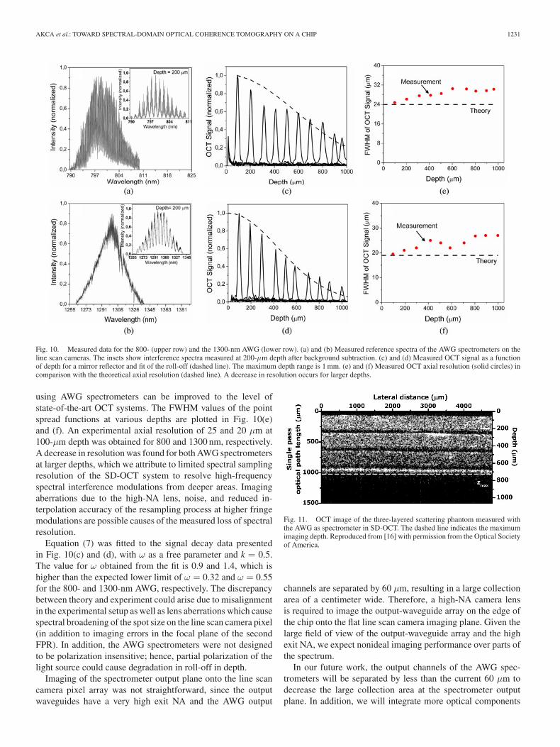
Fig. 10. Measured data for the 800- (upper row) and the 1300-nm AWG (lower row). (a) and (b) Measured reference spectra of the AWG spectrometers on theline scan cameras. The insets show interference spectra measured at 200-μm depth after background subtraction. (c) and (d) Measured OCT signal as a functionof depth for a mirror reflector and fit of the roll-off (dashed line). The maximum depth range is 1 mm. (e) and (f) Measured OCT axial resolution (solid circles) incomparison with the theoretical axial resolution (dashed line). A decrease in resolution occurs for larger depths.
using AWG spectrometers can be improved to the level ofstate-of-the-art OCT systems. The FWHM values of the pointspread functions at various depths are plotted in Fig. 10(e)and (f). An experimental axial resolution of 25 and 20 μm at100-μm depth was obtained for 800 and 1300 nm, respectively.A decrease in resolution was found for both AWG spectrometersat larger depths, which we attribute to limited spectral samplingresolution of the SD-OCT system to resolve high-frequencyspectral interference modulations from deeper areas. Imagingaberrations due to the high-NA lens, noise, and reduced in-terpolation accuracy of the resampling process at higher fringemodulations are possible causes of the measured loss of spectralresolution.
Equation (7) was fitted to the signal decay data presentedin Fig. 10(c) and (d), with ω as a free parameter and k = 0.5.The value for ω obtained from the fit is 0.9 and 1.4, which ishigher than the expected lower limit of ω = 0.32 and ω = 0.55for the 800- and 1300-nm AWG, respectively. The discrepancybetween theory and experiment could arise due to misalignmentin the experimental setup as well as lens aberrations which causespectral broadening of the spot size on the line scan camera pixel(in addition to imaging errors in the focal plane of the secondFPR). In addition, the AWG spectrometers were not designedto be polarization insensitive; hence, partial polarization of thelight source could cause degradation in roll-off in depth.
Imaging of the spectrometer output plane onto the line scancamera pixel array was not straightforward, since the outputwaveguides have a very high exit NA and the AWG output
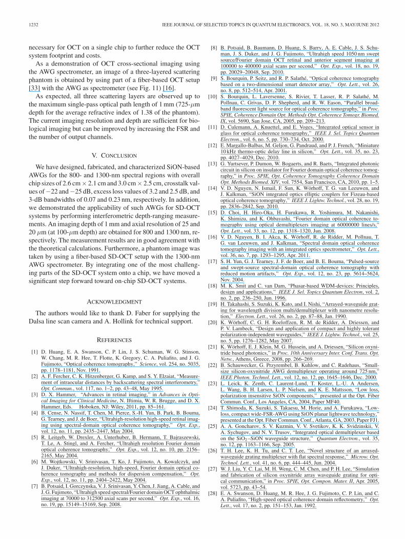
Fig. 11. OCT image of the three-layered scattering phantom measured withthe AWG as spectrometer in SD-OCT. The dashed line indicates the maximumimaging depth. Reproduced from [16] with permission from the Optical Societyof America.
channels are separated by 60 μm, resulting in a large collectionarea of a centimeter wide. Therefore, a high-NA camera lensis required to image the output-waveguide array on the edge ofthe chip onto the flat line scan camera imaging plane. Given thelarge field of view of the output-waveguide array and the highexit NA, we expect nonideal imaging performance over parts ofthe spectrum.
In our future work, the output channels of the AWG spec-trometers will be separated by less than the current 60 μm todecrease the large collection area at the spectrometer outputplane. In addition, we will integrate more optical components
1232 IEEE JOURNAL OF SELECTED TOPICS IN QUANTUM ELECTRONICS, VOL. 18, NO. 3, MAY/JUNE 2012
necessary for OCT on a single chip to further reduce the OCTsystem footprint and costs.
As a demonstration of OCT cross-sectional imaging usingthe AWG spectrometer, an image of a three-layered scatteringphantom is obtained by using part of a fiber-based OCT setup[33] with the AWG as spectrometer (see Fig. 11) [16].
As expected, all three scattering layers are observed up tothe maximum single-pass optical path length of 1 mm (725-μmdepth for the average refractive index of 1.38 of the phantom).The current imaging resolution and depth are sufficient for bio-logical imaging but can be improved by increasing the FSR andthe number of output channels.
V. CONCLUSION
We have designed, fabricated, and characterized SiON-basedAWGs for the 800- and 1300-nm spectral regions with overallchip sizes of 2.6 cm× 2.1 cm and 3.0 cm× 2.5 cm, crosstalk val-ues of−22 and−25 dB, excess loss values of 3.2 and 2.5 dB, and3-dB bandwidths of 0.07 and 0.23 nm, respectively. In addition,we demonstrated the applicability of such AWGs for SD-OCTsystems by performing interferometric depth-ranging measure-ments. An imaging depth of 1 mm and axial resolution of 25 and20 μm (at 100-μm depth) are obtained for 800 and 1300 nm, re-spectively. The measurement results are in good agreement withthe theoretical calculations. Furthermore, a phantom image wastaken by using a fiber-based SD-OCT setup with the 1300-nmAWG spectrometer. By integrating one of the most challeng-ing parts of the SD-OCT system onto a chip, we have moved asignificant step forward toward on-chip SD-OCT systems.
ACKNOWLEDGMENT
The authors would like to thank D. Faber for supplying theDalsa line scan camera and A. Hollink for technical support.
REFERENCES
[1] D. Huang, E. A. Swanson, C. P. Lin, J. S. Schuman, W. G. Stinson,W. Chang, M. R. Hee, T. Flotte, K. Gregory, C. A. Puliafito, and J. G.Fujimoto, “Optical coherence tomography,” Science, vol. 254, no. 5035,pp. 1178–1181, Nov. 1991.
[2] A. F. Fercher, C. K. Hitzenberger, G. Kamp, and S. Y. Elzaiat, “Measure-ment of intraocular distances by backscattering spectral interferometry,”Opt. Commun., vol. 117, no. 1–2, pp. 43–48, May 1995.
[3] D. X. Hammer, “Advances in retinal imaging,” in Advances in Opti-cal Imaging for Clinical Medicine, N. Iftimia, W. R. Brugge, and D. X.Hammer, Eds. Hoboken, NJ: Wiley, 2011, pp. 85–161.
[4] B. Cense, N. Nassif, T. Chen, M. Pierce, S.-H. Yun, B. Park, B. Bouma,G. Tearney, and J. de Boer, “Ultrahigh-resolution high-speed retinal imag-ing using spectral-domain optical coherence tomography,” Opt. Exp.,vol. 12, no. 11, pp. 2435–2447, May 2004.
[5] R. Leitgeb, W. Drexler, A. Unterhuber, B. Hermann, T. Bajraszewski,T. Le, A. Stingl, and A. Fercher, “Ultrahigh resolution Fourier domainoptical coherence tomography,” Opt. Exp., vol. 12, no. 10, pp. 2156–2165, May 2004.
[6] M. Wojtkowski, V. Srinivasan, T. Ko, J. Fujimoto, A. Kowalczyk, andJ. Duker, “Ultrahigh-resolution, high-speed, Fourier domain optical co-herence tomography and methods for dispersion compensation,” Opt.Exp., vol. 12, no. 11, pp. 2404–2422, May 2004.
[7] B. Potsaid, I. Gorczynska, V. J. Srinivasan, Y. Chen, J. Jiang, A. Cable, andJ. G. Fujimoto, “Ultrahigh speed spectral/Fourier domain OCT ophthalmicimaging at 70000 to 312500 axial scans per second,” Opt. Exp., vol. 16,no. 19, pp. 15149–15169, Sep. 2008.
[8] B. Potsaid, B. Baumann, D. Huang, S. Barry, A. E. Cable, J. S. Schu-man, J. S. Duker, and J. G. Fujimoto, “Ultrahigh speed 1050 nm sweptsource/Fourier domain OCT retinal and anterior segment imaging at100000 to 400000 axial scans per second,” Opt. Exp., vol. 18, no. 19,pp. 20029–20048, Sep. 2010.
[9] S. Bourquin, P. Seitz, and R. P. Salathe, “Optical coherence tomographybased on a two-dimensional smart detector array,” Opt. Lett., vol. 26,no. 8, pp. 512–514, Apr. 2001.
[10] S. Bourquin, L. Laversenne, S. Rivier, T. Lasser, R. P. Salathe, M.Pollnau, C. Grivas, D. P. Shepherd, and R. W. Eason, “Parallel broad-band fluorescent light source for optical coherence tomography,” in Proc.SPIE, Coherence Domain Opt. Methods Opt. Coherence Tomogr. Biomed.IX, vol. 5690, San Jose, CA, 2005, pp. 209–213.
[11] D. Culemann, A. Knuettel, and E. Voges, “Integrated optical sensor inglass for optical coherence tomography,” IEEE J. Sel. Topics QuantumElectron., vol. 6, no. 5, pp. 730–734, Oct. 2000.
[12] E. Margallo-Balbas, M. Geljon, G. Pandraud, and P. J. French, “Miniature10 kHz thermo-optic delay line in silicon,” Opt. Lett., vol. 35, no. 23,pp. 4027–4029, Dec. 2010.
[13] G. Yurtsever, P. Dumon, W. Bogaerts, and R. Baets, “Integrated photoniccircuit in silicon on insulator for Fourier domain optical coherence tomog-raphy,” in Proc. SPIE, Opt. Coherence Tomography Coherence DomainOpt. Methods Biomed. XIV, vol. 7554, San Francisco, CA, 2010, pp. 1–5.
[14] V. D. Nguyen, N. Ismail, F. Sun, K. Worhoff, T. G. van Leeuwen, andJ. Kalkman, “SiON integrated optics elliptic couplers for Fizeau-basedoptical coherence tomography,” IEEE J. Lightw. Technol., vol. 28, no. 19,pp. 2836–2842, Sep. 2010.
[15] D. Choi, H. Hiro-Oka, H. Furukawa, R. Yoshimura, M. Nakanishi,K. Shimizu, and K. Ohbayashi, “Fourier domain optical coherence to-mography using optical demultiplexers imaging at 60000000 lines/s,”Opt. Lett., vol. 33, no. 12, pp. 1318–1320, Jun. 2008.
[16] V. D. Nguyen, B. I. Akca, K. Worhoff, R. de Ridder, M. Pollnau, T.G. van Leeuwen, and J. Kalkman, “Spectral domain optical coherencetomography imaging with an integrated optics spectrometer,” Opt. Lett.,vol. 36, no. 7, pp. 1293–1295, Apr. 2011.
[17] S. H. Yun, G. J. Tearney, J. F. de Boer, and B. E. Bouma, “Pulsed-sourceand swept-source spectral-domain optical coherence tomography withreduced motion artifacts,” Opt. Exp., vol. 12, no. 23, pp. 5614–5624,Nov. 2004.
[18] M. K. Smit and C. van Dam, “Phasar-based WDM-devices: Principles,design and applications,” IEEE J. Sel. Topics Quantum Electron, vol. 2,no. 2, pp. 236–250, Jun. 1996.
[19] H. Takahashi, S. Suzuki, K. Kato, and I. Nishi, “Arrayed-waveguide grat-ing for wavelength division multi/demultiplexer with nanometre resolu-tion,” Electron. Lett., vol. 26, no. 2, pp. 87–88, Jan. 1990.
[20] K. Worhoff, C. G. H. Roeloffzen, R. M. de Ridder, A. Driessen, andP. V. Lambeck, “Design and application of compact and highly tolerantpolarization-independent waveguides,” IEEE J. Lightw. Technol., vol. 25,no. 5, pp. 1276–1282, May 2007.
[21] K. Worhoff, E. J. Klein, M. G. Hussein, and A. Driessen, “Silicon oxyni-tride based photonics,” in Proc. 10th Anniversary Inter. Conf. Trans. Opt.Netw., Athens, Greece, 2008, pp. 266–269.
[22] B. Schauwecker, G. Przyrembel, B. Kuhlow, and C. Radehaus, “Small-size silicon-oxynitride AWG demultiplexer operating around 725 nm,”IEEE Photon. Technol. Lett., vol. 12, no. 12, pp. 1645–1646, Dec. 2000.
[23] L. Leick, K. Zenth, C. Laurent-Lund, T. Koster, L.-U. A Andersen,L. Wang, B. H. Larsen, L. P. Nielsen, and K. E. Mattsson, “Low loss,polarization insensitive SiON components,” presented at the Opt. FiberCommun. Conf., Los Angeles, CA, 2004, Paper MF40.
[24] T. Shimoda, K. Suzuki, S. Takaesu, M. Horie, and A. Furukawa, “Low-loss, compact wide-FSR-AWG using SiON planar lightwave technology,”presented at the Opt. Fiber Commun. Conf., Atlanta, GA, 2003, Paper FJ1.
[25] A. A. Goncharov, S. V. Kuzmin, V. V. Svetikov, K. K. Svidzinskii, V.A. Sychugov, and N. V. Trusov, “Integrated optical demultiplexer basedon the SiO2 –SiON waveguide structure,” Quantum Electron., vol. 35,no. 12, pp. 1163–1166, Sep. 2005.
[26] T. H. Lee, K. H. Tu, and C. T. Lee, “Novel structure of an arrayed-waveguide grating multiplexer with flat spectral response,” Microw. Opt.Technol. Lett., vol. 41, no. 6, pp. 444–445, Jun. 2004.
[27] W. J. Liu, Y. C. Lai, M. H. Weng, C. M. Chen, and P. H. Lee, “Simulationand fabrication of silicon oxynitride array waveguide grating for opti-cal communication,” in Proc. SPIE, Opt. Compon. Mater. II, Apr. 2005,vol. 5723, pp. 43–54.
[28] E. A. Swanson, D. Huang, M. R. Hee, J. G. Fujimoto, C. P. Lin, and C.A. Puliafito, “High-speed optical coherence domain reflectometry,” Opt.Lett., vol. 17, no. 2, pp. 151–153, Jan. 1992.
AKCA et al.: TOWARD SPECTRAL-DOMAIN OPTICAL COHERENCE TOMOGRAPHY ON A CHIP 1233
[29] G. Hausler and M. W. Lindner, “‘Coherence radar’ and ‘spectral radar’—New tools for dermatological diagnosis,” J. Biomed. Opt., vol. 3, no. 1,pp. 21–31, Jan. 1998.
[30] Z. Hu, Y. Pan, and A. M. Rollins, “Analytical model of spectrometer-based two-beam spectral interferometry,” Appl. Opt., vol. 46, no. 35,pp. 8499–8505, Dec. 2007.
[31] S. H. Yun, G. J. Tearney, B. E. Bouma, B. H. Park, and J. F. de Boer,“High-speed spectral-domain optical coherence tomography at 1.3 μmwavelength,” Opt. Exp., vol. 11, no. 26, pp. 3598–3604, Dec. 2003.
[32] R. W. Chuang and Z. L. Liao, “2 × 2 thermo-optic silicon oxynitride op-tical switch based on the integrated multimode interference waveguides,”J. Electrochem. Soc., vol. 157, no. 2, pp. H149–H152, Dec. 2009.
[33] J. Kalkman, A. V. Bykov, D. J. Faber, and T. G. van Leeuwen, “Multipleand dependent scattering effects in Doppler optical coherence tomogra-phy,” Opt. Exp., vol. 18, no. 4, pp. 3883–3892, Feb. 2010.
B. Imran Akca received the B.Sc. degree from the Department of Electricaland Electronics Engineering and the M.Sc. degree from the Institute of MaterialScience and Nanotechnology both from Bilkent University, Ankara, Turkey, in2006 and 2008, respectively. She is currently working toward the Ph.D. degreein the area of integrated optics in the Integrated Optical MicroSystems Group,MESA+ Institute for Nanotechnology, University of Twente, Enschede, TheNetherlands.
Her research interests include designing integrated arrayed waveguide gratingspectrometers for optical coherence tomography systems.
Van Duc Nguyen received the M.Sc. degree in physics from the University ofCentral Florida, Orlando, in 2008. He is currently working toward the Ph.D.degree in the Department of Biomedical Engineering and Physics, AcademicMedical Center, University of Amsterdam, Amsterdam, The Netherlands.
His research interests include the usage of integrated optics in optical coher-ence tomography (OCT) and on functional OCT.
Jeroen Kalkman received the M.Sc. degree in experimental physics from theVrije Universiteit Amsterdam, Amsterdam, The Netherlands, and the Ph.D. de-gree from the Institute for Atomic and Molecular Physics, Amsterdam, wherehe was involved in erbium-doped photonic materials.
After doing research for two years at Philips NatLab, Eindhoven, TheNetherlands, he joined the Academic Medical Center, University of Amsterdam,Amsterdam, where he has been involved in optical coherence tomography, lighttissue interactions, and integrated optics for healthcare applications.
Nur Ismail was born in Palermo, Italy, in 1977. He received the B.S. degreein electronic engineering from the University of Palermo, Palermo, Italy, in2002, the M.S. degree in information technology and telecommunications fromthe Research Center for Electronics in Sicily, Monreale, Italy, in 2003, and theM.Sc. degree in photonics and optoelectronics from the University of Rome“Roma Tre,” Rome, Italy, in 2006. He is currently working toward the Ph.D.degree in the Integrated Optical MicroSystems Group, MESA+ Institute forNanotechnology, University of Twente, Enschede, The Netherlands.
Between 2003 and 2006, he was involved in the field of information tech-nology in Rome, Italy.
Gabriel Sengo received the B.Sc. degree in applied physics from the Polytechnicof Enschede, Enschede, The Netherlands, in 1995.
After having been active in industry for a number of years, he joined as aTechnician the Integrated Optical Micro Systems Group, MESA+ Institute forNanotechnology, University of Twente, Enschede. He specializes in lithographyand reactive ion etching.
Fei Sun received the M.S. degree in microelectronics from Xi’an JiaotongUniversity, Xi’an, China, and the Ph.D. degree in optoelectronics from theInstitute of Semiconductors, Chinese Academy of Sciences, Beijing, China, in2001 and 2006, respectively.
He is currently a Scientist at the Institute of Microelectronics, A∗STAR,Singapore.
Alfred Driessen received the M.Sc. degree in experimental physics andthe Ph.D. degree in quantum solids from the University of Amsterdam,Amsterdam, The Netherlands, in 1972 and 1982, respectively.
After a period as a Postdoctoral Researcher at Free University, Amsterdam,where he was involved in metal hydrides, he joined the Lightwave DevicesGroup, University of Twente, Enschede, The Netherlands, as an Associate Pro-fessor in 1988. His research field from then is integrated optics for opticalcommunication and optical nonlinear devices. From 2003 to 2009, he was aFull Professor within the Integrated Optical Micro Systems Group, MESA+Institute for Nanotechnology, University of Twente. He is the author or coau-thor of more than 250 refereed journal and conference papers and three patents.His research interests include compact and complex nanophotonic structuresthat can be applied in sensing, communication, and spectroscopy.
Ton G. van Leeuwen studied physics at the University of Amsterdam,Amsterdam, The Netherlands, and received the Ph.D. degree from the Labora-tory of Experimental Cardiology, University of Utrecht, Utrecht, The Nether-lands, in 1993.
He is currently the Head of the Department of Biomedical Engineering andPhysics, Academic Medical Center, University of Amsterdam, and a Profes-sor in the Biomedical Photonic Imaging Group, MIRA Institute for Biomed-ical Technology and Technical Medicine, University of Twente, Enschede,The Netherlands. His research interests include the clinical application ofbiomedical optics.
Markus Pollnau received the M.Sc. degree from the University of Hamburg,Hamburg, Germany, in 1992, and the Ph.D. degree from the University of Bern,Bern, Switzerland, in 1996, both in physics.
After postdoctoral positions with the University of Southampton and theUniversity of Bern, he was a Project and Research Group Leader with theSwiss Federal Institute of Technology, Lausanne, Switzerland. In 2004, hebecame a Full Professor and the Chair of the Integrated Optical MicroSystemsGroup, MESA+ Institute for Nanotechnology, University of Twente, Enschede,The Netherlands. He has contributed to more than 400 reviewed journal andinternational conference papers and six book chapters in the fields of crystaland thin-film growth, rare-earth-ion spectroscopy, solid-state and fiber lasers,and waveguide fabrication, devices, and applications.
Dr. Pollnau has held European, Swiss, and Dutch personal Fellowshipsand has obtained numerous National and European Research Grants. He hasbeen involved in the organization of major international conferences, e.g., asa Program and General Co-chair of the Conference on Lasers and Electro-Optics (2006/2008) and the Conference on Lasers and Electro-Optics Europe(2009/2011), and served as the Topical Editor for the Journal of the OpticalSociety of America B.
Kerstin Worhoff received the M.Sc. degree in optoelectronics from the Tech-nical University of Bratislava, Bratislava, Slovakia, and the Ph.D. degree inapplied physics from the University of Twente, Enschede, The Netherlands, in1991 and 1996, respectively.
In 1996, she joined the Lightwave Devices Group (now Integrated Opti-cal MicroSystems Group, MESA+ Institute for Nanotechnology), Universityof Twente, as a Postdoctoral Researcher, where since 2000 she has been anAssistant Professor. Her research interests include the field of active and passivesilicon-based photonics technology, rare-earth-ion-doped devices, and opticalwaveguide design.
Rene M. de Ridder (M’94) was born in Amsterdam, The Netherlands, in 1950.He received the M.S. and Ph.D. degrees in electrical engineering from the Uni-versity of Twente, Enschede, The Netherlands, in 1978 and 1988, respectively.His thesis was focused on sensitive thin-film magnetic-field sensors.
Since 1981, he has been a Lecturer and a Research Scientist at the Universityof Twente, where he is currently a member of the Integrated Optical MicroSys-tems Group, MESA+ Institute for Nanotechnology. In 1988, he was involved inresearch in integrated optical devices. A basis for his research in this field waslaid during a half year of sabbatical leave at AT&T Bell Labs, Holmdel, NJ, in1989. His research interests include photonic crystal structures and wavelength-selective devices for applications in sensing and communication.
Related Documents