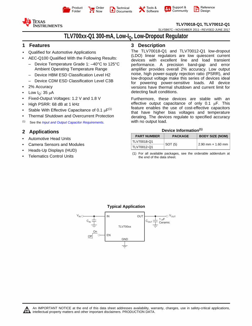
TLV700xx GND EN IN OUT V IN V OUT On Off C IN C OUT 1 F Ceramic m Product Folder Order Now Technical Documents Tools & Software Support & Community Reference Design An IMPORTANT NOTICE at the end of this data sheet addresses availability, warranty, changes, use in safety-critical applications, intellectual property matters and other important disclaimers. PRODUCTION DATA. TLV70018-Q1, TLV70012-Q1 SLVSB67C – NOVEMBER 2011 – REVISED JUNE 2017 TLV700xx-Q1 300-mA, Low-I Q , Low-Dropout Regulator 1 1 Features 1• Qualified for Automotive Applications • AEC-Q100 Qualified With the Following Results: – Device Temperature Grade 1: –40°C to 125°C Ambient Operating Temperature Range – Device HBM ESD Classification Level H2 – Device CDM ESD Classification Level C3B • 2% Accuracy • Low I Q : 35 μA • Fixed-Output Voltages: 1.2 V and 1.8 V • High PSRR: 68 dB at 1 kHz • Stable With Effective Capacitance of 0.1 μF (1) • Thermal Shutdown and Overcurrent Protection (1) See the Input and Output Capacitor Requirements. 2 Applications • Automotive Head Units • Camera Sensors and Modules • Heads-Up Displays (HUD) • Telematics Control Units 3 Description The TLV70018-Q1 and TLV70012-Q1 low-dropout (LDO) linear regulators are low quiescent current devices with excellent line and load transient performance. A precision band-gap and error amplifier provides overall 2% accuracy. Low output noise, high power-supply rejection ratio (PSRR), and low-dropout voltage make this series of devices ideal for powering power-sensitive loads. All device versions have thermal shutdown and current limit for detecting fault conditions. Furthermore, these devices are stable with an effective output capacitance of only 0.1 μF. This feature enables the use of cost-effective capacitors that have higher bias voltages and temperature derating. The devices regulate to specified accuracy with no output load. Device Information (1) PART NUMBER PACKAGE BODY SIZE (NOM) TLV70018-Q1 SOT (5) 2.90 mm × 1.60 mm TLV70012-Q1 (1) For all available packages, see the orderable addendum at the end of the data sheet. SPACE SPACE SPACE SPACE SPACE SPACE Typical Application

Welcome message from author
This document is posted to help you gain knowledge. Please leave a comment to let me know what you think about it! Share it to your friends and learn new things together.
Transcript
TLV700xx
GND
EN
IN OUTVIN
VOUT
On
Off
CIN
COUT
1 F
Ceramic
m
Product
Folder
Order
Now
Technical
Documents
Tools &
Software
Support &Community
ReferenceDesign
An IMPORTANT NOTICE at the end of this data sheet addresses availability, warranty, changes, use in safety-critical applications,intellectual property matters and other important disclaimers. PRODUCTION DATA.
TLV70018-Q1, TLV70012-Q1SLVSB67C –NOVEMBER 2011–REVISED JUNE 2017
TLV700xx-Q1 300-mA, Low-IQ, Low-Dropout Regulator
1
1 Features1• Qualified for Automotive Applications• AEC-Q100 Qualified With the Following Results:
– Device Temperature Grade 1: –40°C to 125°CAmbient Operating Temperature Range
– Device HBM ESD Classification Level H2– Device CDM ESD Classification Level C3B
• 2% Accuracy• Low IQ: 35 μA• Fixed-Output Voltages: 1.2 V and 1.8 V• High PSRR: 68 dB at 1 kHz• Stable With Effective Capacitance of 0.1 μF(1)
• Thermal Shutdown and Overcurrent Protection(1) See the Input and Output Capacitor Requirements.
2 Applications• Automotive Head Units• Camera Sensors and Modules• Heads-Up Displays (HUD)• Telematics Control Units
3 DescriptionThe TLV70018-Q1 and TLV70012-Q1 low-dropout(LDO) linear regulators are low quiescent currentdevices with excellent line and load transientperformance. A precision band-gap and erroramplifier provides overall 2% accuracy. Low outputnoise, high power-supply rejection ratio (PSRR), andlow-dropout voltage make this series of devices idealfor powering power-sensitive loads. All deviceversions have thermal shutdown and current limit fordetecting fault conditions.
Furthermore, these devices are stable with aneffective output capacitance of only 0.1 μF. Thisfeature enables the use of cost-effective capacitorsthat have higher bias voltages and temperaturederating. The devices regulate to specified accuracywith no output load.
Device Information(1)
PART NUMBER PACKAGE BODY SIZE (NOM)TLV70018-Q1
SOT (5) 2.90 mm × 1.60 mmTLV70012-Q1
(1) For all available packages, see the orderable addendum atthe end of the data sheet.
SPACE
SPACE
SPACE
SPACE
SPACE
SPACE
Typical Application
2
TLV70018-Q1, TLV70012-Q1SLVSB67C –NOVEMBER 2011–REVISED JUNE 2017 www.ti.com
Product Folder Links: TLV70018-Q1 TLV70012-Q1
Submit Documentation Feedback Copyright © 2011–2017, Texas Instruments Incorporated
Table of Contents1 Features .................................................................. 12 Applications ........................................................... 13 Description ............................................................. 14 Revision History..................................................... 25 Pin Configuration and Functions ......................... 46 Specifications......................................................... 5
6.1 Absolute Maximum Ratings ...................................... 56.2 ESD Ratings.............................................................. 56.3 Recommended Operating Conditions....................... 56.4 Thermal Information .................................................. 56.5 Electrical Characteristics........................................... 66.6 Typical Characteristics .............................................. 7
7 Detailed Description ............................................ 117.1 Overview ................................................................. 117.2 Functional Block Diagrams ..................................... 117.3 Feature Description................................................. 117.4 Device Functional Modes........................................ 12
8 Application and Implementation ........................ 13
8.1 Application Information............................................ 138.2 Typical Application .................................................. 13
9 Power Supply Recommendations ...................... 1410 Layout................................................................... 15
10.1 Layout Guidelines ................................................. 1510.2 Layout Example .................................................... 1510.3 Thermal Considerations ........................................ 1510.4 Power Dissipation ................................................. 15
11 Device and Documentation Support ................. 1711.1 Device Support...................................................... 1711.2 Documentation Support ........................................ 1711.3 Related Links ........................................................ 1711.4 Receiving Notification of Documentation Updates 1711.5 Community Resources.......................................... 1711.6 Trademarks ........................................................... 1711.7 Electrostatic Discharge Caution............................ 1711.8 Glossary ................................................................ 17
12 Mechanical, Packaging, and OrderableInformation ........................................................... 18
4 Revision HistoryNOTE: Page numbers for previous revisions may differ from page numbers in the current version.
Changes from Revision B (January 2016) to Revision C Page
• Changed Fixed-Output Voltage Features bullet from Fixed-Output Voltage Combinations Possible from 1.2 V to 4.8V to Fixed-Output Voltages: 1.2 V and 1.8 V ......................................................................................................................... 1
• Changed Applications section ............................................................................................................................................... 1• Changed first paragraph of Description section: changed TLV700xx-Q1 series to TLV70018-Q1 and TLV70012-Q1,
deleted second sentence, changed a wide selection of battery-operated handheld equipment to powering power-sensitive loads, and changed safety to detecting fault conditions.......................................................................................... 1
• Deleted Fixed-Voltage Version from Typical Application title ................................................................................................ 1• Changed Input voltage parameter: changed symbol from VI to VIN, moved EN and OUT rows to standalone
parameters ............................................................................................................................................................................. 5• Changed maximum specification of Output voltage parameter from 5.5 V to 1.8 V ............................................................. 5• Added IOUT symbol to Current output parameter ................................................................................................................... 5• Deleted TLV70018-Q1 column from Thermal Information table ............................................................................................ 5• Added TLV70018-Q1 to TLV70012-Q1 column in Thermal Information table; all thermal values for TLV70018-Q1
changed to the TLV70012-Q1 thermal values........................................................................................................................ 5• Changed VOUT(TYP) to VOUT(NOM) in conditions statement of Electrical Characteristics table .................................................. 6• Changed symbols for Line regulation, Load regulation, and Output noise voltage parameters from ΔVO/ΔVIN to
ΔVOUT/ΔVIN, ΔVO/ΔIOUT to ΔVOUT/ΔIOUT, and VN to Vn (respectively) in Electrical Characteristics table.................................. 6• Changed VOUT(TYP) to VOUT(NOM) in Typical Characteristics conditions statement .................................................................. 7• Deleted Dropout Voltage vs Input Voltage and Dropout Voltage vs Output Current curves ................................................. 7• Changed TLV700xx-Q1 to TLV70018-Q1 and TLV70012-Q1 in Overview section ............................................................. 11• Added TLV70012-Q1 to sub-sections of Feature Description and Device Functional Modes sections .............................. 11• Changed 160°C to 165°C, 140°C to 145°C, and 35°C to 40°C in Thermal Shutdown section .......................................... 12• Changed Application Information section: changed first two sentences, deleted second paragraph ................................. 13• Changed Example Value column values for 2nd and 3rd rows in Design Parameters table............................................... 13• Added TLV70012-Q1 to Input and Output Capacitor Requirements section ....................................................................... 14• Deleted first and last paragraphs from Thermal Considerations section ............................................................................ 15
3
TLV70018-Q1, TLV70012-Q1www.ti.com SLVSB67C –NOVEMBER 2011–REVISED JUNE 2017
Product Folder Links: TLV70018-Q1 TLV70012-Q1
Submit Documentation FeedbackCopyright © 2011–2017, Texas Instruments Incorporated
Revision History (continued)• Deleted second sentence from second paragraph of Power Dissipation section ............................................................... 15• Added TLV70012-Q1 to Power Dissipation section ............................................................................................................ 15
Changes from Revision A (March 2012) to Revision B Page
• Added ESD Ratings table, Recommended Operating Conditions table, Thermal Information table, DetailedDescription section, Application and Implementation section, Application and Implementation section, Layoutsection, Device and Documentation Support section, and Mechanical, Packaging, and Orderable Information section...... 1
• Deleted the Dissipation Ratings table..................................................................................................................................... 5
OUT
NC
IN
GND
EN
1
2
3
5
4
4
TLV70018-Q1, TLV70012-Q1SLVSB67C –NOVEMBER 2011–REVISED JUNE 2017 www.ti.com
Product Folder Links: TLV70018-Q1 TLV70012-Q1
Submit Documentation Feedback Copyright © 2011–2017, Texas Instruments Incorporated
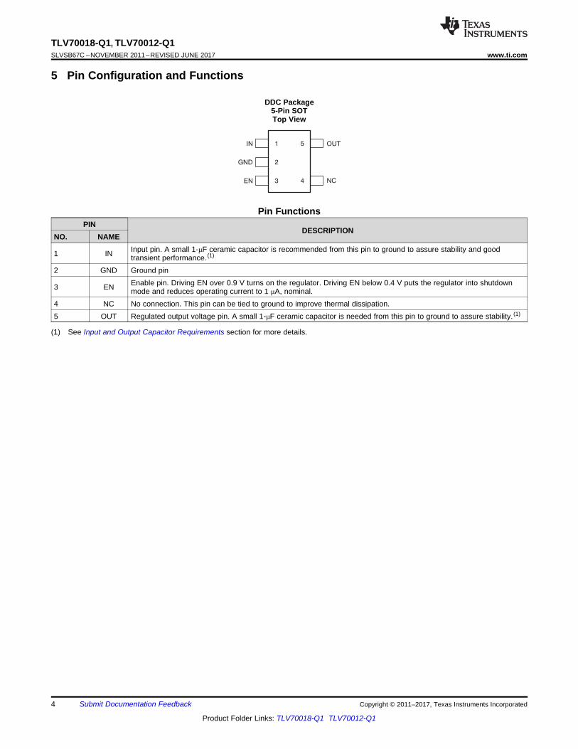
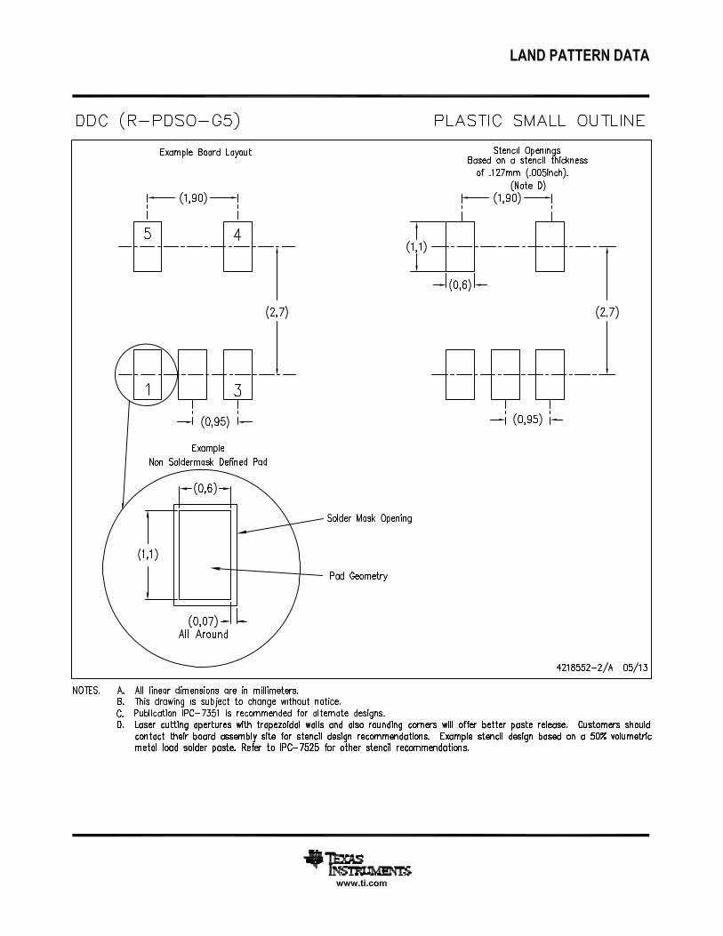
5 Pin Configuration and Functions
DDC Package5-Pin SOTTop View
(1) See Input and Output Capacitor Requirements section for more details.
Pin FunctionsPIN
DESCRIPTIONNO. NAME
1 IN Input pin. A small 1-μF ceramic capacitor is recommended from this pin to ground to assure stability and goodtransient performance. (1)
2 GND Ground pin
3 EN Enable pin. Driving EN over 0.9 V turns on the regulator. Driving EN below 0.4 V puts the regulator into shutdownmode and reduces operating current to 1 μA, nominal.
4 NC No connection. This pin can be tied to ground to improve thermal dissipation.5 OUT Regulated output voltage pin. A small 1-μF ceramic capacitor is needed from this pin to ground to assure stability. (1)

5
TLV70018-Q1, TLV70012-Q1www.ti.com SLVSB67C –NOVEMBER 2011–REVISED JUNE 2017
Product Folder Links: TLV70018-Q1 TLV70012-Q1
Submit Documentation FeedbackCopyright © 2011–2017, Texas Instruments Incorporated
(1) Stresses beyond those listed under Absolute Maximum Ratings may cause permanent damage to the device. These are stress ratingsonly, which do not imply functional operation of the device at these or any other conditions beyond those indicated under RecommendedOperating Conditions. Exposure to absolute-maximum-rated conditions for extended periods may affect device reliability.
(2) All voltages are with respect to network ground terminal.
6 Specifications
6.1 Absolute Maximum Ratingsover operating free-air temperature range, unless otherwise noted. (1)
MIN MAX UNIT
Voltage (2)
IN –0.3 6.0 VEN –0.3 6.0 VOUT –0.3 6.0 V
Current (source) OUT Internally LimitedOutput short-circuit duration IndefiniteOperating virtual junction, TJ –55 150 °CStorage temperature, Tstg –55 150 °C
(1) AEC Q100-002 indicates that HBM stressing shall be in accordance with the ANSI/ESDA/JEDEC JS-001 specification.
6.2 ESD RatingsVALUE UNIT
V(ESD) Electrostatic dischargeHuman-body model (HBM), per AEC Q100-002 (1) 2000
VCharged-device model (CDM), per AEC Q100-011 750
6.3 Recommended Operating Conditionsover operating free-air temperature range, unless otherwise noted.
MIN MAX UNITVIN Input voltage IN 2 5.5 VVEN Enable voltage EN 0 5.5 VVOUT Output voltage OUT 0 1.8 VIOUT Current output 0 300 mATJ Operating junction temperature –40 150 °C
(1) For more information about traditional and new thermal metrics, see the Semiconductor and IC Package Thermal Metrics applicationreport.
6.4 Thermal Information
THERMAL METRIC (1)
TLV70018-Q1,TLV70012-Q1
UNITDDC (SOT)5 PINS
RθJA Junction-to-ambient thermal resistance 262.8 °C/WRθJC(top) Junction-to-case (top) thermal resistance 68.2 °C/WRθJB Junction-to-board thermal resistance 81.6 °C/WψJT Junction-to-top characterization parameter 1.1 °C/WψJB Junction-to-board characterization parameter 80.9 °C/WRθJC(bot) Junction-to-case (bottom) thermal resistance NA °C/W
6
TLV70018-Q1, TLV70012-Q1SLVSB67C –NOVEMBER 2011–REVISED JUNE 2017 www.ti.com
Product Folder Links: TLV70018-Q1 TLV70012-Q1
Submit Documentation Feedback Copyright © 2011–2017, Texas Instruments Incorporated
(1) Startup time = time from EN assertion to 0.98 × VOUT(NOM).
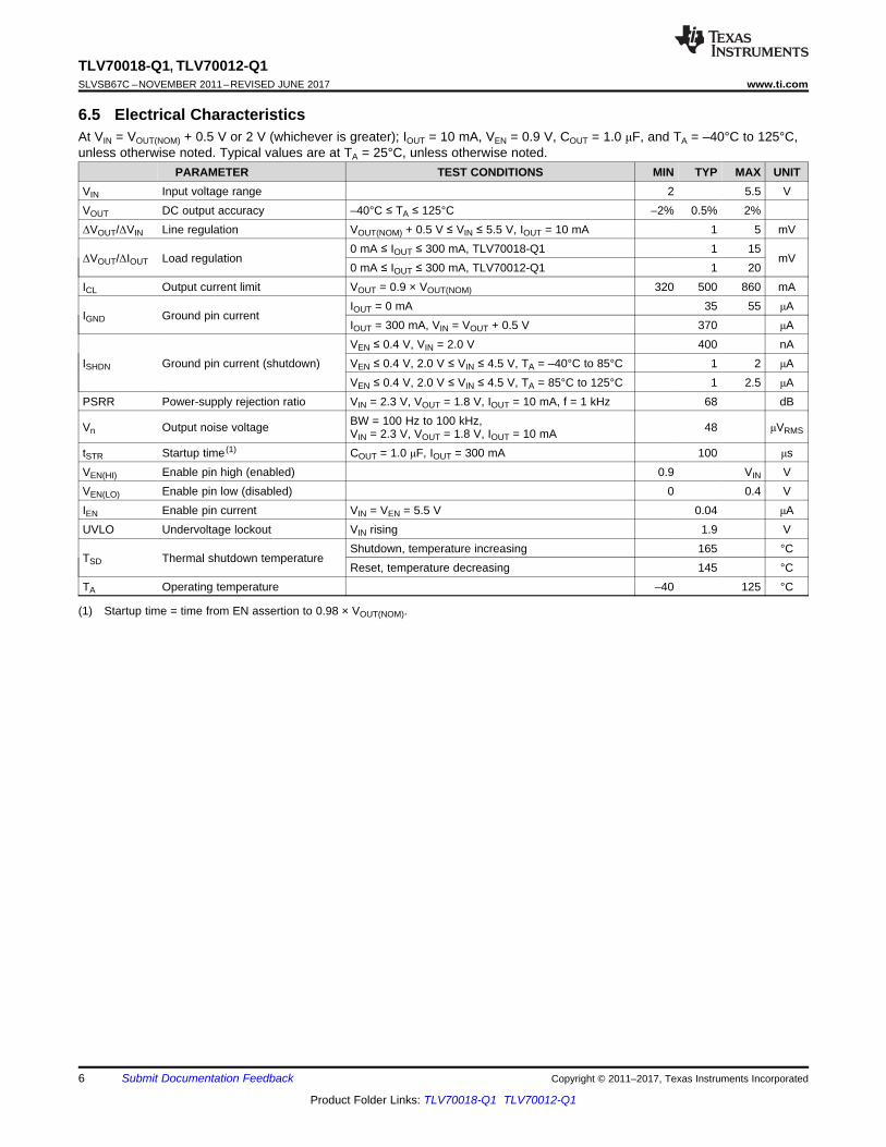
6.5 Electrical CharacteristicsAt VIN = VOUT(NOM) + 0.5 V or 2 V (whichever is greater); IOUT = 10 mA, VEN = 0.9 V, COUT = 1.0 μF, and TA = –40°C to 125°C,unless otherwise noted. Typical values are at TA = 25°C, unless otherwise noted.
PARAMETER TEST CONDITIONS MIN TYP MAX UNITVIN Input voltage range 2 5.5 VVOUT DC output accuracy –40°C ≤ TA ≤ 125°C –2% 0.5% 2%ΔVOUT/ΔVIN Line regulation VOUT(NOM) + 0.5 V ≤ VIN ≤ 5.5 V, IOUT = 10 mA 1 5 mV
ΔVOUT/ΔIOUT Load regulation0 mA ≤ IOUT ≤ 300 mA, TLV70018-Q1 1 15
mV0 mA ≤ IOUT ≤ 300 mA, TLV70012-Q1 1 20
ICL Output current limit VOUT = 0.9 × VOUT(NOM) 320 500 860 mA
IGND Ground pin currentIOUT = 0 mA 35 55 μAIOUT = 300 mA, VIN = VOUT + 0.5 V 370 μA
ISHDN Ground pin current (shutdown)VEN ≤ 0.4 V, VIN = 2.0 V 400 nAVEN ≤ 0.4 V, 2.0 V ≤ VIN ≤ 4.5 V, TA = –40°C to 85°C 1 2 μAVEN ≤ 0.4 V, 2.0 V ≤ VIN ≤ 4.5 V, TA = 85°C to 125°C 1 2.5 μA
PSRR Power-supply rejection ratio VIN = 2.3 V, VOUT = 1.8 V, IOUT = 10 mA, f = 1 kHz 68 dB
Vn Output noise voltage BW = 100 Hz to 100 kHz,VIN = 2.3 V, VOUT = 1.8 V, IOUT = 10 mA 48 μVRMS
tSTR Startup time (1) COUT = 1.0 μF, IOUT = 300 mA 100 μsVEN(HI) Enable pin high (enabled) 0.9 VIN VVEN(LO) Enable pin low (disabled) 0 0.4 VIEN Enable pin current VIN = VEN = 5.5 V 0.04 μAUVLO Undervoltage lockout VIN rising 1.9 V
TSD Thermal shutdown temperatureShutdown, temperature increasing 165 °CReset, temperature decreasing 145 °C
TA Operating temperature –40 125 °C
50
45
40
35
30
25
20
15
10
5
0
I GN
D(
Am
)
2.1 2.6 3.1 3.6 4.1 4.6 5.1
V (V)IN
5.6
+125 C°
+85 C°
+25 C°
-40 C°
V = 1.8 VOUT
450
400
350
300
250
200
150
100
50
0
I GN
D(m
A)
0
I (mA)OUT
300
+125 C°
+85 C°
+25 C°
-40 C°
V = 1.8 VOUT
50 150 250100 200
0 100 150 300
I (mA)OUT
1.90
1.88
1.86
1.84
1.82
1.80
1.78
1.76
1.74
1.72
1.70
V(V
)O
UT
50 200
+125 C°
+85 C°
+25 C°
-40 C°
V = 1.8 VOUT
250
1.90
1.88
1.86
1.84
1.82
1.80
1.78
1.76
1.74
1.72
1.70
V(V
)O
UT
-40 -25 -10 5 20 35 50 65 80 95 110
Temperature ( C)°
125
10mA
150mA
200mA
V = 1.8 VOUT
1.90
1.88
1.86
1.84
1.82
1.80
1.78
1.76
1.74
1.72
1.70
VO
UT
(V)
2.1 2.6 3.1 3.6 4.1 4.6 5.1
V (V)IN
5.6
+125 C°
+85 C°
+25 C°
-40 C°
V = 1.8 V
I = 10 mAOUT
OUT
1.90
1.88
1.86
1.84
1.82
1.80
1.78
1.76
1.74
1.72
1.70
VO
UT
(V)
2.3 2.7 3.1 3.5 3.9 4.3 4.7
V (V)IN
5.55.1
+125 C°
+85 C°
+25 C°
-40 C°
V = 1.8 V
I = 300 mAOUT
OUT
7
TLV70018-Q1, TLV70012-Q1www.ti.com SLVSB67C –NOVEMBER 2011–REVISED JUNE 2017
Product Folder Links: TLV70018-Q1 TLV70012-Q1
Submit Documentation FeedbackCopyright © 2011–2017, Texas Instruments Incorporated
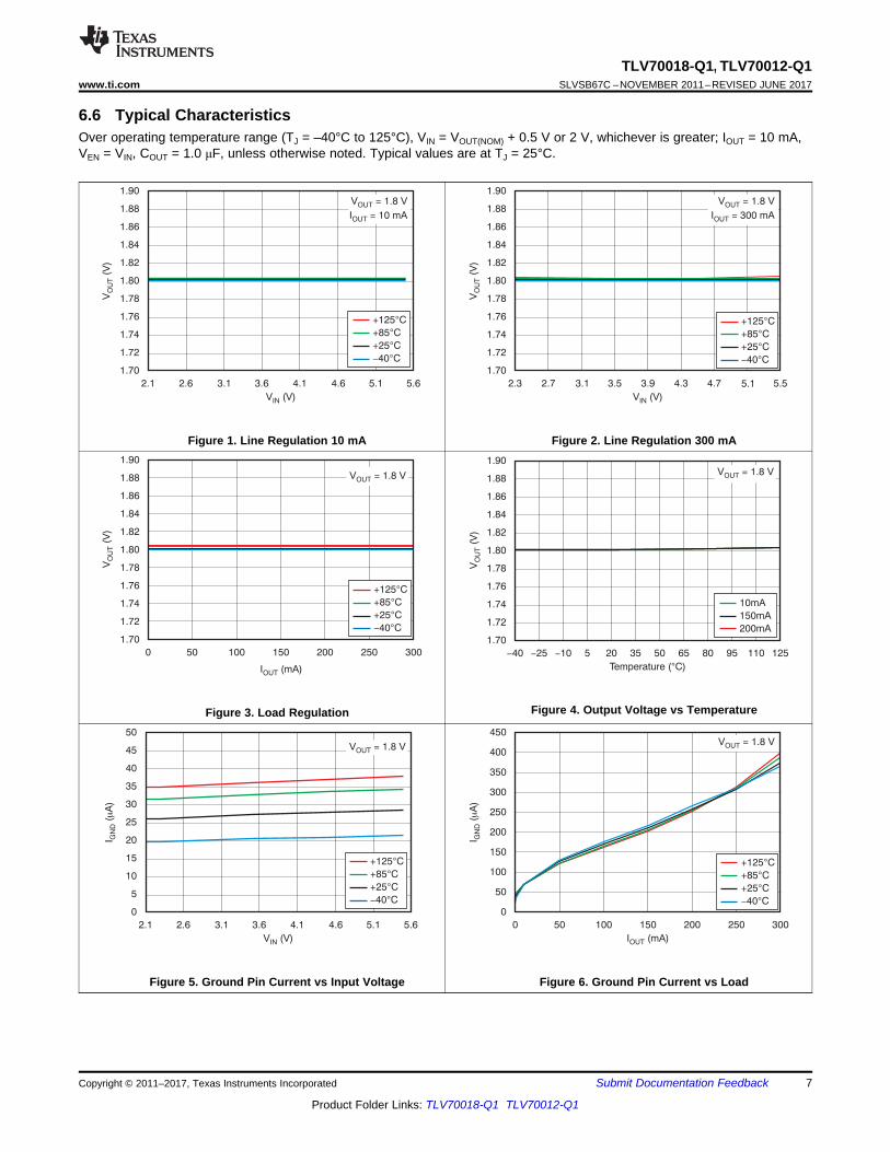
6.6 Typical CharacteristicsOver operating temperature range (TJ = –40°C to 125°C), VIN = VOUT(NOM) + 0.5 V or 2 V, whichever is greater; IOUT = 10 mA,VEN = VIN, COUT = 1.0 μF, unless otherwise noted. Typical values are at TJ = 25°C.
Figure 1. Line Regulation 10 mA Figure 2. Line Regulation 300 mA
Figure 3. Load Regulation Figure 4. Output Voltage vs Temperature
Figure 5. Ground Pin Current vs Input Voltage Figure 6. Ground Pin Current vs Load
2.1 2.2 2.3 2.4 2.5 2.6 2.7 2.8
Input Voltage (V)
80
70
60
50
40
30
20
10
0
PS
RR
(d
B)
10 kHz
100 kHz
1 kHz V = 1.8 VOUT
10
1
0.1
0.01
0.001
Ou
tpu
t S
pe
ctr
al N
ois
e D
en
sity (
V/
)m
ÖH
z
10 100 1 k 10 k 100 k 1 M 10 M
Frequency (Hz)
V = 1.8 VOUT
I = 10 mA
C = C = 1 FOUT
IN OUT m
100
90
80
70
60
50
40
30
20
10
0
PS
RR
(dB
)
10 100 1 k 10 k 100 k 1 M 10 M
Frequency (Hz)
I = 150 mAOUT
I = 10 mAOUT
V V = 0.5 VIN OUT-
700
600
500
400
300
200
100
0
I LIM
(mA
)
2.3 2.7 3.1 3.5 3.9 4.3 4.7
V (V)IN
5.55.1
V = 1.8 VOUT
+125 C°
+85 C°
+25 C°
-40 C°
50
45
40
35
30
25
20
15
10
5
0
I(
A)
mG
ND
-40 -25 -10 5 20 35 50 65 80 95 110
Temperature ( C)°
125
V = 1.8 VOUT
2.5
2
1.5
1
0.5
0
I SH
DN
(A
m)
2.1 2.6 3.1 3.6 4.1 4.6 5.1
V (V)IN
5.6
+125 C°
+85 C°
+25 C°
-40 C°
V = 1.8 VOUT
8
TLV70018-Q1, TLV70012-Q1SLVSB67C –NOVEMBER 2011–REVISED JUNE 2017 www.ti.com
Product Folder Links: TLV70018-Q1 TLV70012-Q1
Submit Documentation Feedback Copyright © 2011–2017, Texas Instruments Incorporated
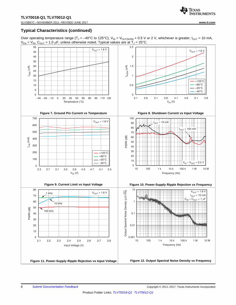
Typical Characteristics (continued)Over operating temperature range (TJ = –40°C to 125°C), VIN = VOUT(NOM) + 0.5 V or 2 V, whichever is greater; IOUT = 10 mA,VEN = VIN, COUT = 1.0 μF, unless otherwise noted. Typical values are at TJ = 25°C.
Figure 7. Ground Pin Current vs Temperature Figure 8. Shutdown Current vs Input Voltage
Figure 9. Current Limit vs Input Voltage Figure 10. Power-Supply Ripple Rejection vs Frequency
Figure 11. Power-Supply Ripple Rejection vs Input Voltage Figure 12. Output Spectral Noise Density vs Frequency
1 V
/div
5 m
V/d
iv
1 ms/div
VOUT
Slew Rate = 1 V/ sm
VIN
2.9 V
2.3 V
V = 1.8 V
I 300 mA
OUT
OUT =
1 V
/div
5 m
V/d
iv
1 ms/div
VOUT
VIN 2.9 V
2.3 V
V = 1.8 V
I 1 mA
OUT
OUT =
Slew Rate = 1 V/ sm
50
mA
/div
20
mV
/div
10 s/divm
VOUT
IOUT 50 mA
0 mA
t = t = 1 sR F m
VOUT = 1.8 V
200 m
A/d
iv100 m
V/d
iv
10 s/divm
VOUT
300 mA
0 mA
t = t = sR F
m1
IOUT
VOUT
= 1.8 V
10
0 m
A/d
iv5
0 m
V/d
iv
10 s/divm
VOUT
IOUT
200 mA
0 mA
t = t = 1 sR F m
VOUT = 1.8 V
20
mA
/div
5 m
V/d
iv
10 s/divm
VOUT
VOUT = 1.8 V
IOUT
10 mA
0 mA
t = t = 1 sR F m
9
TLV70018-Q1, TLV70012-Q1www.ti.com SLVSB67C –NOVEMBER 2011–REVISED JUNE 2017
Product Folder Links: TLV70018-Q1 TLV70012-Q1
Submit Documentation FeedbackCopyright © 2011–2017, Texas Instruments Incorporated
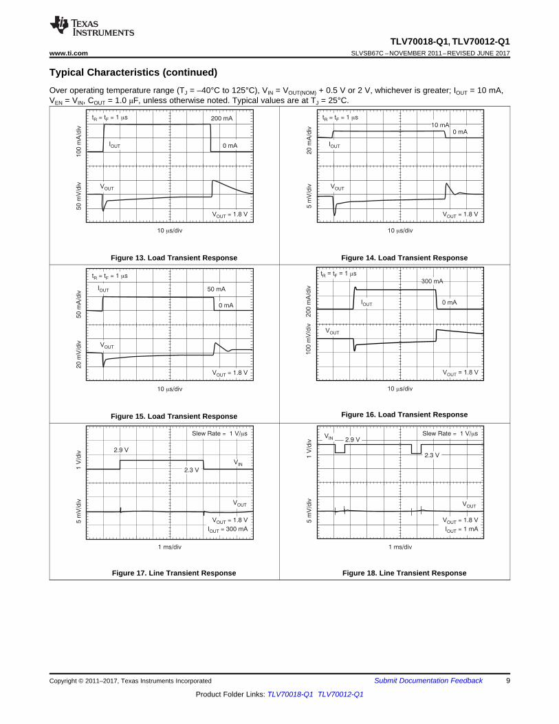
Typical Characteristics (continued)Over operating temperature range (TJ = –40°C to 125°C), VIN = VOUT(NOM) + 0.5 V or 2 V, whichever is greater; IOUT = 10 mA,VEN = VIN, COUT = 1.0 μF, unless otherwise noted. Typical values are at TJ = 25°C.
Figure 13. Load Transient Response Figure 14. Load Transient Response
Figure 15. Load Transient Response Figure 16. Load Transient Response
Figure 17. Line Transient Response Figure 18. Line Transient Response
1 V
/div
10
mV
/div
1 ms/div
Slew Rate = 1 V/ sm
V = 1.8 V
I = 300 mA
OUT
OUT5.5 V
VIN2.1 V
VOUT
1 V
/div
200 ms/div
VOUT
VIN
V = 1.8 VOUT
I 1 mAOUT =
10
TLV70018-Q1, TLV70012-Q1SLVSB67C –NOVEMBER 2011–REVISED JUNE 2017 www.ti.com
Product Folder Links: TLV70018-Q1 TLV70012-Q1
Submit Documentation Feedback Copyright © 2011–2017, Texas Instruments Incorporated
Typical Characteristics (continued)Over operating temperature range (TJ = –40°C to 125°C), VIN = VOUT(NOM) + 0.5 V or 2 V, whichever is greater; IOUT = 10 mA,VEN = VIN, COUT = 1.0 μF, unless otherwise noted. Typical values are at TJ = 25°C.
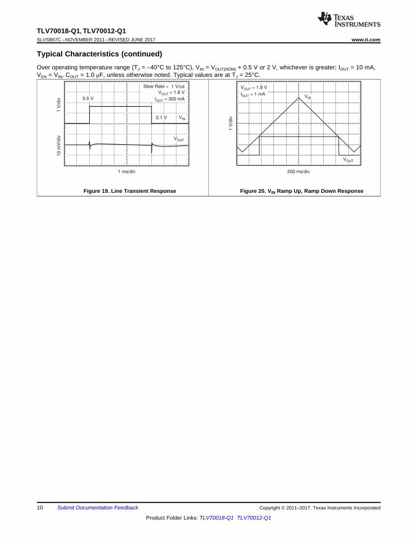
Figure 19. Line Transient Response Figure 20. VIN Ramp Up, Ramp Down Response
ThermalShutdown
CurrentLimit
UVLO
Bandgap
IN
EN
OUT
LOGIC
GND
TLV700xx Series
11
TLV70018-Q1, TLV70012-Q1www.ti.com SLVSB67C –NOVEMBER 2011–REVISED JUNE 2017
Product Folder Links: TLV70018-Q1 TLV70012-Q1
Submit Documentation FeedbackCopyright © 2011–2017, Texas Instruments Incorporated
7 Detailed Description
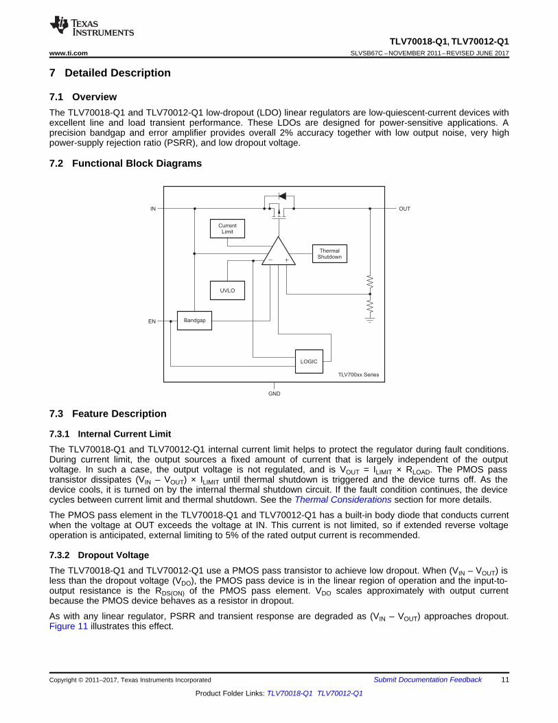
7.1 OverviewThe TLV70018-Q1 and TLV70012-Q1 low-dropout (LDO) linear regulators are low-quiescent-current devices withexcellent line and load transient performance. These LDOs are designed for power-sensitive applications. Aprecision bandgap and error amplifier provides overall 2% accuracy together with low output noise, very highpower-supply rejection ratio (PSRR), and low dropout voltage.
7.2 Functional Block Diagrams
7.3 Feature Description
7.3.1 Internal Current LimitThe TLV70018-Q1 and TLV70012-Q1 internal current limit helps to protect the regulator during fault conditions.During current limit, the output sources a fixed amount of current that is largely independent of the outputvoltage. In such a case, the output voltage is not regulated, and is VOUT = ILIMIT × RLOAD. The PMOS passtransistor dissipates (VIN – VOUT) × ILIMIT until thermal shutdown is triggered and the device turns off. As thedevice cools, it is turned on by the internal thermal shutdown circuit. If the fault condition continues, the devicecycles between current limit and thermal shutdown. See the Thermal Considerations section for more details.
The PMOS pass element in the TLV70018-Q1 and TLV70012-Q1 has a built-in body diode that conducts currentwhen the voltage at OUT exceeds the voltage at IN. This current is not limited, so if extended reverse voltageoperation is anticipated, external limiting to 5% of the rated output current is recommended.
7.3.2 Dropout VoltageThe TLV70018-Q1 and TLV70012-Q1 use a PMOS pass transistor to achieve low dropout. When (VIN – VOUT) isless than the dropout voltage (VDO), the PMOS pass device is in the linear region of operation and the input-to-output resistance is the RDS(ON) of the PMOS pass element. VDO scales approximately with output currentbecause the PMOS device behaves as a resistor in dropout.
As with any linear regulator, PSRR and transient response are degraded as (VIN – VOUT) approaches dropout.Figure 11 illustrates this effect.
12
TLV70018-Q1, TLV70012-Q1SLVSB67C –NOVEMBER 2011–REVISED JUNE 2017 www.ti.com
Product Folder Links: TLV70018-Q1 TLV70012-Q1
Submit Documentation Feedback Copyright © 2011–2017, Texas Instruments Incorporated
Feature Description (continued)7.3.3 Undervoltage Lockout (UVLO)The TLV70018-Q1 and TLV70012-Q1 use an undervoltage lockout circuit to keep the output shut off until internalcircuitry is operating properly.
7.3.4 Thermal ShutdownThermal protection disables the output when the junction temperature rises to approximately 165°C, allowing thedevice to cool. When the junction temperature cools to approximately 145°C, the output circuitry is againenabled. Depending on power dissipation, thermal resistance, and ambient temperature, the thermal protectioncircuit may cycle on and off. This cycling limits the dissipation of the regulator, protecting it from damage as aresult of overheating.
Any tendency to activate the thermal protection circuit indicates excessive power dissipation or an inadequateheatsink. For reliable operation, junction temperature should be limited to 125°C maximum. To estimate themargin of safety in a complete design (including heatsink), increase the ambient temperature until the thermalprotection is triggered; use worst-case loads and signal conditions. For good reliability, thermal protection shouldtrigger at least 40°C above the maximum expected ambient condition of the particular application. Thisconfiguration produces a worst-case junction temperature of 125°C at the highest expected ambient temperatureand worst-case load.
The internal protection circuitry of the TLV70018-Q1 and TLV70012-Q1 has been designed to protect againstoverload conditions. It was not intended to replace proper heatsinking. Continuously running the TLV70018-Q1 orTLV70012-Q1 into thermal shutdown degrades device reliability.
7.4 Device Functional Modes
7.4.1 ShutdownThe enable pin (EN) is active high. The device is enabled when voltage at EN pin goes above 0.9 V. Thisrelatively lower value of voltage required to turn the LDO on can be exploited to power the LDO with a GPIO ofrecent processors whose GPIO Logic 1 voltage level is lower than traditional microcontrollers. The device isturned off when the EN pin is held at less than 0.4 V. When shutdown capability is not required, EN can beconnected to the IN pin.
7.4.2 Operation with VIN Less than 2 VThe TLV70018-Q1 and TLV70012-Q1 devices operate with input voltages above 2 V. The typical UVLO voltageis 1.9 V and the device operates at an input voltage above 2 V. When input voltage falls below UVLO voltage,the device will shutdown.
7.4.3 Operation with VIN Greater than 2 VWhen VIN is greater than 2 V, if input voltage is higher than desired output voltage plus dropout voltage, theoutput voltage is equal to the desired value. Otherwise, output voltage will be VIN minus dropout voltage.
IN
EN
GND
1 uF 1 uF
OUT
VIN
VOUT
TLV700xx-Q1
13
TLV70018-Q1, TLV70012-Q1www.ti.com SLVSB67C –NOVEMBER 2011–REVISED JUNE 2017
Product Folder Links: TLV70018-Q1 TLV70012-Q1
Submit Documentation FeedbackCopyright © 2011–2017, Texas Instruments Incorporated
8 Application and Implementation
NOTEInformation in the following applications sections is not part of the TI componentspecification, and TI does not warrant its accuracy or completeness. TI’s customers areresponsible for determining suitability of components for their purposes. Customers shouldvalidate and test their design implementation to confirm system functionality.
8.1 Application InformationThe TLV70018-Q1 and TLV70012-Q1 consume low quiescent current and deliver excellent line and loadtransient performance. These characteristics, combined with low noise and very good PSRR with little (VIN –VOUT) headroom, make this family of devices ideal for portable RF applications. This family of regulators offerscurrent limit and thermal protection, and is specified from –40°C to 125°C.
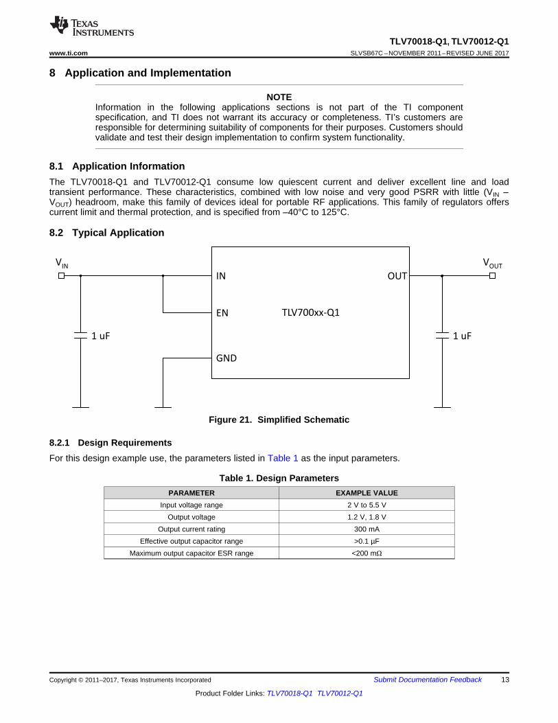
8.2 Typical Application
Figure 21. Simplified Schematic
8.2.1 Design RequirementsFor this design example use, the parameters listed in Table 1 as the input parameters.
Table 1. Design ParametersPARAMETER EXAMPLE VALUE
Input voltage range 2 V to 5.5 VOutput voltage 1.2 V, 1.8 V
Output current rating 300 mAEffective output capacitor range >0.1 µF
Maximum output capacitor ESR range <200 mΩ
14
TLV70018-Q1, TLV70012-Q1SLVSB67C –NOVEMBER 2011–REVISED JUNE 2017 www.ti.com
Product Folder Links: TLV70018-Q1 TLV70012-Q1
Submit Documentation Feedback Copyright © 2011–2017, Texas Instruments Incorporated
8.2.2 Detailed Design Procedure
8.2.2.1 Input and Output Capacitor Requirements1.0-μF X5R- and X7R-type ceramic capacitors are recommended because these capacitors have minimalvariation in value and equivalent series resistance (ESR) over temperature.
However, the TLV70018-Q1 and TLV70012-Q1 are designed to be stable with an effective capacitance of 0.1 μFor larger at the output. Thus, the device is stable with capacitors of other dielectric types as well, as long as theeffective capacitance under operating bias voltage and temperature is greater than 0.1 μF. This effectivecapacitance refers to the capacitance that the LDO sees under operating bias voltage and temperatureconditions; that is, the capacitance after taking both bias voltage and temperature derating into consideration. Inaddition to allowing the use of lower-cost dielectrics, this capability of being stable with 0.1-μF effectivecapacitance also enables the use of smaller-footprint capacitors that have higher derating in size- and space-constrained applications.
NOTEUsing a 0.1-μF rated capacitor at the output of the LDO does not ensure stability becausethe effective capacitance under the specified operating conditions would be less than0.1 μF. Maximum ESR should be less than 200 mΩ.
Although an input capacitor is not required for stability, it is good analog design practice to connect a 0.1-μF to1.0-μF, low ESR capacitor across the IN pin and GND pin of the regulator. This capacitor counteracts reactiveinput sources and improves transient response, noise rejection, and ripple rejection. A higher-value capacitormay be necessary if large, fast rise-time load transients are anticipated, or if the device is not located close to thepower source. If source impedance is more than 2 Ω, a 0.1-μF input capacitor may be necessary to ensurestability.
8.2.2.2 Transient ResponseAs with any regulator, increasing the size of the output capacitor reduces overshoot or undershoot magnitude butincreases the duration of the transient response.
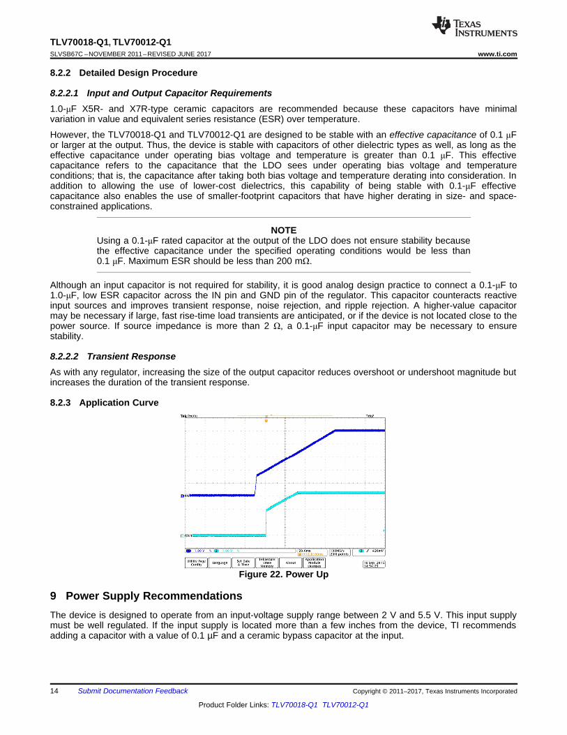
8.2.3 Application Curve
Figure 22. Power Up
9 Power Supply RecommendationsThe device is designed to operate from an input-voltage supply range between 2 V and 5.5 V. This input supplymust be well regulated. If the input supply is located more than a few inches from the device, TI recommendsadding a capacitor with a value of 0.1 µF and a ceramic bypass capacitor at the input.
1
2
3
5
4
IN
EN
GND
OUT
N/C
15
TLV70018-Q1, TLV70012-Q1www.ti.com SLVSB67C –NOVEMBER 2011–REVISED JUNE 2017
Product Folder Links: TLV70018-Q1 TLV70012-Q1
Submit Documentation FeedbackCopyright © 2011–2017, Texas Instruments Incorporated
10 Layout
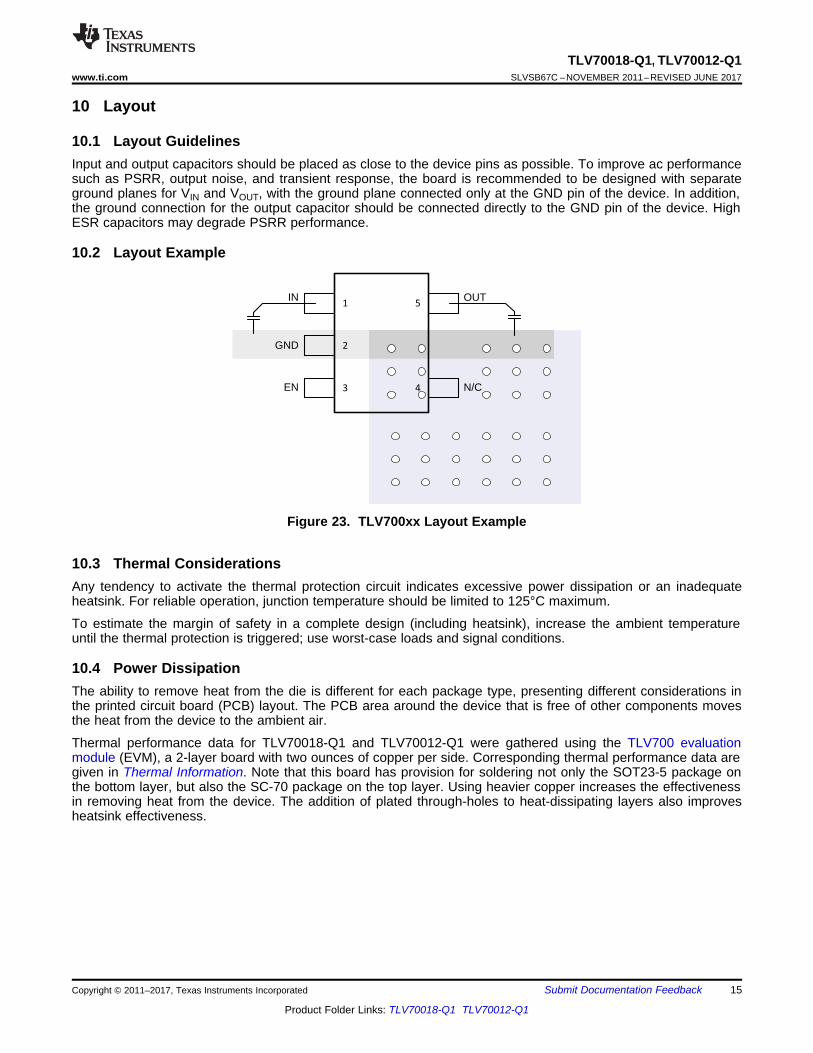
10.1 Layout GuidelinesInput and output capacitors should be placed as close to the device pins as possible. To improve ac performancesuch as PSRR, output noise, and transient response, the board is recommended to be designed with separateground planes for VIN and VOUT, with the ground plane connected only at the GND pin of the device. In addition,the ground connection for the output capacitor should be connected directly to the GND pin of the device. HighESR capacitors may degrade PSRR performance.
10.2 Layout Example
Figure 23. TLV700xx Layout Example
10.3 Thermal ConsiderationsAny tendency to activate the thermal protection circuit indicates excessive power dissipation or an inadequateheatsink. For reliable operation, junction temperature should be limited to 125°C maximum.
To estimate the margin of safety in a complete design (including heatsink), increase the ambient temperatureuntil the thermal protection is triggered; use worst-case loads and signal conditions.
10.4 Power DissipationThe ability to remove heat from the die is different for each package type, presenting different considerations inthe printed circuit board (PCB) layout. The PCB area around the device that is free of other components movesthe heat from the device to the ambient air.
Thermal performance data for TLV70018-Q1 and TLV70012-Q1 were gathered using the TLV700 evaluationmodule (EVM), a 2-layer board with two ounces of copper per side. Corresponding thermal performance data aregiven in Thermal Information. Note that this board has provision for soldering not only the SOT23-5 package onthe bottom layer, but also the SC-70 package on the top layer. Using heavier copper increases the effectivenessin removing heat from the device. The addition of plated through-holes to heat-dissipating layers also improvesheatsink effectiveness.
A max Jmax JA DT T (R P )q
= - ´
J A JA DT T T (R P )q
D = - = ´
J A JA DT T (R P )q
= + ´
D OUT IN OUT Q INP I (V V ) I V= ´ - + ´
16
TLV70018-Q1, TLV70012-Q1SLVSB67C –NOVEMBER 2011–REVISED JUNE 2017 www.ti.com
Product Folder Links: TLV70018-Q1 TLV70012-Q1
Submit Documentation Feedback Copyright © 2011–2017, Texas Instruments Incorporated
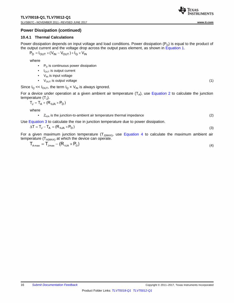
Power Dissipation (continued)10.4.1 Thermal CalculationsPower dissipation depends on input voltage and load conditions. Power dissipation (PD) is equal to the product ofthe output current and the voltage drop across the output pass element, as shown in Equation 1.
where• PD is continuous power dissipation• IOUT is output current• VIN is input voltage• VOUT is output voltage (1)
Since IQ << IOUT, the term IQ × VIN is always ignored.
For a device under operation at a given ambient air temperature (TA), use Equation 2 to calculate the junctiontemperature (TJ).
where• ZθJA is the junction-to-ambient air temperature thermal impedance (2)
Use Equation 3 to calculate the rise in junction temperature due to power dissipation.(3)
For a given maximum junction temperature (TJ(MAX), use Equation 4 to calculate the maximum ambient airtemperature (TA(MAX) at which the device can operate.
(4)
17
TLV70018-Q1, TLV70012-Q1www.ti.com SLVSB67C –NOVEMBER 2011–REVISED JUNE 2017
Product Folder Links: TLV70018-Q1 TLV70012-Q1
Submit Documentation FeedbackCopyright © 2011–2017, Texas Instruments Incorporated
11 Device and Documentation Support
11.1 Device Support
11.1.1 Package MountingSolder pad footprint recommendations for the TLV70018-Q1 are available from the Texas Instruments web siteat www.ti.com.
11.2 Documentation Support
11.2.1 Related DocumentationFor related documentation, see the following:
TLV700 evaluation module
11.3 Related LinksThe table below lists quick access links. Categories include technical documents, support and communityresources, tools and software, and quick access to order now.
Table 2. Related Links
PARTS PRODUCT FOLDER ORDER NOW TECHNICALDOCUMENTS
TOOLS &SOFTWARE
SUPPORT &COMMUNITY
TLV70018-Q1 Click here Click here Click here Click here Click hereTLV70012-Q1 Click here Click here Click here Click here Click here
11.4 Receiving Notification of Documentation UpdatesTo receive notification of documentation updates, navigate to the device product folder on ti.com. In the upperright corner, click on Alert me to register and receive a weekly digest of any product information that haschanged. For change details, review the revision history included in any revised document.
11.5 Community ResourcesThe following links connect to TI community resources. Linked contents are provided "AS IS" by the respectivecontributors. They do not constitute TI specifications and do not necessarily reflect TI's views; see TI's Terms ofUse.
TI E2E™ Online Community TI's Engineer-to-Engineer (E2E) Community. Created to foster collaborationamong engineers. At e2e.ti.com, you can ask questions, share knowledge, explore ideas and helpsolve problems with fellow engineers.
Design Support TI's Design Support Quickly find helpful E2E forums along with design support tools andcontact information for technical support.
11.6 TrademarksE2E is a trademark of Texas Instruments.All other trademarks are the property of their respective owners.
11.7 Electrostatic Discharge CautionThis integrated circuit can be damaged by ESD. Texas Instruments recommends that all integrated circuits be handled withappropriate precautions. Failure to observe proper handling and installation procedures can cause damage.
ESD damage can range from subtle performance degradation to complete device failure. Precision integrated circuits may be moresusceptible to damage because very small parametric changes could cause the device not to meet its published specifications.
11.8 GlossarySLYZ022 — TI Glossary.
This glossary lists and explains terms, acronyms, and definitions.
18
TLV70018-Q1, TLV70012-Q1SLVSB67C –NOVEMBER 2011–REVISED JUNE 2017 www.ti.com
Product Folder Links: TLV70018-Q1 TLV70012-Q1
Submit Documentation Feedback Copyright © 2011–2017, Texas Instruments Incorporated
12 Mechanical, Packaging, and Orderable InformationThe following pages include mechanical, packaging, and orderable information. This information is the mostcurrent data available for the designated devices. This data is subject to change without notice and revision ofthis document. For browser-based versions of this data sheet, refer to the left-hand navigation.

PACKAGE OPTION ADDENDUM
www.ti.com 28-Mar-2017
Addendum-Page 1
PACKAGING INFORMATION
Orderable Device Status(1)
Package Type PackageDrawing
Pins PackageQty
Eco Plan(2)
Lead/Ball Finish(6)
MSL Peak Temp(3)
Op Temp (°C) Device Marking(4/5)
Samples
TLV70012QDDCRQ1 ACTIVE SOT-23-THIN DDC 5 3000 Green (RoHS& no Sb/Br)
CU NIPDAU Level-2-260C-1 YEAR -40 to 125 SDO
TLV70018QDDCRQ1 ACTIVE SOT-23-THIN DDC 5 3000 Green (RoHS& no Sb/Br)
CU NIPDAU Level-2-260C-1 YEAR -40 to 125 DAL
(1) The marketing status values are defined as follows:ACTIVE: Product device recommended for new designs.LIFEBUY: TI has announced that the device will be discontinued, and a lifetime-buy period is in effect.NRND: Not recommended for new designs. Device is in production to support existing customers, but TI does not recommend using this part in a new design.PREVIEW: Device has been announced but is not in production. Samples may or may not be available.OBSOLETE: TI has discontinued the production of the device.
(2) Eco Plan - The planned eco-friendly classification: Pb-Free (RoHS), Pb-Free (RoHS Exempt), or Green (RoHS & no Sb/Br) - please check http://www.ti.com/productcontent for the latest availabilityinformation and additional product content details.TBD: The Pb-Free/Green conversion plan has not been defined.Pb-Free (RoHS): TI's terms "Lead-Free" or "Pb-Free" mean semiconductor products that are compatible with the current RoHS requirements for all 6 substances, including the requirement thatlead not exceed 0.1% by weight in homogeneous materials. Where designed to be soldered at high temperatures, TI Pb-Free products are suitable for use in specified lead-free processes.Pb-Free (RoHS Exempt): This component has a RoHS exemption for either 1) lead-based flip-chip solder bumps used between the die and package, or 2) lead-based die adhesive used betweenthe die and leadframe. The component is otherwise considered Pb-Free (RoHS compatible) as defined above.Green (RoHS & no Sb/Br): TI defines "Green" to mean Pb-Free (RoHS compatible), and free of Bromine (Br) and Antimony (Sb) based flame retardants (Br or Sb do not exceed 0.1% by weightin homogeneous material)
(3) MSL, Peak Temp. - The Moisture Sensitivity Level rating according to the JEDEC industry standard classifications, and peak solder temperature.
(4) There may be additional marking, which relates to the logo, the lot trace code information, or the environmental category on the device.
(5) Multiple Device Markings will be inside parentheses. Only one Device Marking contained in parentheses and separated by a "~" will appear on a device. If a line is indented then it is a continuationof the previous line and the two combined represent the entire Device Marking for that device.
(6) Lead/Ball Finish - Orderable Devices may have multiple material finish options. Finish options are separated by a vertical ruled line. Lead/Ball Finish values may wrap to two lines if the finishvalue exceeds the maximum column width.
Important Information and Disclaimer:The information provided on this page represents TI's knowledge and belief as of the date that it is provided. TI bases its knowledge and belief on informationprovided by third parties, and makes no representation or warranty as to the accuracy of such information. Efforts are underway to better integrate information from third parties. TI has taken andcontinues to take reasonable steps to provide representative and accurate information but may not have conducted destructive testing or chemical analysis on incoming materials and chemicals.TI and TI suppliers consider certain information to be proprietary, and thus CAS numbers and other limited information may not be available for release.
PACKAGE OPTION ADDENDUM
www.ti.com 28-Mar-2017
Addendum-Page 2
In no event shall TI's liability arising out of such information exceed the total purchase price of the TI part(s) at issue in this document sold by TI to Customer on an annual basis.
TAPE AND REEL INFORMATION
*All dimensions are nominal
Device PackageType
PackageDrawing
Pins SPQ ReelDiameter
(mm)
ReelWidth
W1 (mm)
A0(mm)
B0(mm)
K0(mm)
P1(mm)
W(mm)
Pin1Quadrant
TLV70012QDDCRQ1 SOT-23-THIN
DDC 5 3000 179.0 8.4 3.2 3.2 1.4 4.0 8.0 Q3
TLV70018QDDCRQ1 SOT-23-THIN
DDC 5 3000 180.0 8.4 3.2 3.2 1.4 4.0 8.0 Q3
PACKAGE MATERIALS INFORMATION
www.ti.com 8-May-2018
Pack Materials-Page 1
*All dimensions are nominal
Device Package Type Package Drawing Pins SPQ Length (mm) Width (mm) Height (mm)
TLV70012QDDCRQ1 SOT-23-THIN DDC 5 3000 195.0 200.0 45.0
TLV70018QDDCRQ1 SOT-23-THIN DDC 5 3000 195.0 200.0 45.0
PACKAGE MATERIALS INFORMATION
www.ti.com 8-May-2018
Pack Materials-Page 2
IMPORTANT NOTICE
Texas Instruments Incorporated (TI) reserves the right to make corrections, enhancements, improvements and other changes to itssemiconductor products and services per JESD46, latest issue, and to discontinue any product or service per JESD48, latest issue. Buyersshould obtain the latest relevant information before placing orders and should verify that such information is current and complete.TI’s published terms of sale for semiconductor products (http://www.ti.com/sc/docs/stdterms.htm) apply to the sale of packaged integratedcircuit products that TI has qualified and released to market. Additional terms may apply to the use or sale of other types of TI products andservices.Reproduction of significant portions of TI information in TI data sheets is permissible only if reproduction is without alteration and isaccompanied by all associated warranties, conditions, limitations, and notices. TI is not responsible or liable for such reproduceddocumentation. Information of third parties may be subject to additional restrictions. Resale of TI products or services with statementsdifferent from or beyond the parameters stated by TI for that product or service voids all express and any implied warranties for theassociated TI product or service and is an unfair and deceptive business practice. TI is not responsible or liable for any such statements.Buyers and others who are developing systems that incorporate TI products (collectively, “Designers”) understand and agree that Designersremain responsible for using their independent analysis, evaluation and judgment in designing their applications and that Designers havefull and exclusive responsibility to assure the safety of Designers' applications and compliance of their applications (and of all TI productsused in or for Designers’ applications) with all applicable regulations, laws and other applicable requirements. Designer represents that, withrespect to their applications, Designer has all the necessary expertise to create and implement safeguards that (1) anticipate dangerousconsequences of failures, (2) monitor failures and their consequences, and (3) lessen the likelihood of failures that might cause harm andtake appropriate actions. Designer agrees that prior to using or distributing any applications that include TI products, Designer willthoroughly test such applications and the functionality of such TI products as used in such applications.TI’s provision of technical, application or other design advice, quality characterization, reliability data or other services or information,including, but not limited to, reference designs and materials relating to evaluation modules, (collectively, “TI Resources”) are intended toassist designers who are developing applications that incorporate TI products; by downloading, accessing or using TI Resources in anyway, Designer (individually or, if Designer is acting on behalf of a company, Designer’s company) agrees to use any particular TI Resourcesolely for this purpose and subject to the terms of this Notice.TI’s provision of TI Resources does not expand or otherwise alter TI’s applicable published warranties or warranty disclaimers for TIproducts, and no additional obligations or liabilities arise from TI providing such TI Resources. TI reserves the right to make corrections,enhancements, improvements and other changes to its TI Resources. TI has not conducted any testing other than that specificallydescribed in the published documentation for a particular TI Resource.Designer is authorized to use, copy and modify any individual TI Resource only in connection with the development of applications thatinclude the TI product(s) identified in such TI Resource. NO OTHER LICENSE, EXPRESS OR IMPLIED, BY ESTOPPEL OR OTHERWISETO ANY OTHER TI INTELLECTUAL PROPERTY RIGHT, AND NO LICENSE TO ANY TECHNOLOGY OR INTELLECTUAL PROPERTYRIGHT OF TI OR ANY THIRD PARTY IS GRANTED HEREIN, including but not limited to any patent right, copyright, mask work right, orother intellectual property right relating to any combination, machine, or process in which TI products or services are used. Informationregarding or referencing third-party products or services does not constitute a license to use such products or services, or a warranty orendorsement thereof. Use of TI Resources may require a license from a third party under the patents or other intellectual property of thethird party, or a license from TI under the patents or other intellectual property of TI.TI RESOURCES ARE PROVIDED “AS IS” AND WITH ALL FAULTS. TI DISCLAIMS ALL OTHER WARRANTIES ORREPRESENTATIONS, EXPRESS OR IMPLIED, REGARDING RESOURCES OR USE THEREOF, INCLUDING BUT NOT LIMITED TOACCURACY OR COMPLETENESS, TITLE, ANY EPIDEMIC FAILURE WARRANTY AND ANY IMPLIED WARRANTIES OFMERCHANTABILITY, FITNESS FOR A PARTICULAR PURPOSE, AND NON-INFRINGEMENT OF ANY THIRD PARTY INTELLECTUALPROPERTY RIGHTS. TI SHALL NOT BE LIABLE FOR AND SHALL NOT DEFEND OR INDEMNIFY DESIGNER AGAINST ANY CLAIM,INCLUDING BUT NOT LIMITED TO ANY INFRINGEMENT CLAIM THAT RELATES TO OR IS BASED ON ANY COMBINATION OFPRODUCTS EVEN IF DESCRIBED IN TI RESOURCES OR OTHERWISE. IN NO EVENT SHALL TI BE LIABLE FOR ANY ACTUAL,DIRECT, SPECIAL, COLLATERAL, INDIRECT, PUNITIVE, INCIDENTAL, CONSEQUENTIAL OR EXEMPLARY DAMAGES INCONNECTION WITH OR ARISING OUT OF TI RESOURCES OR USE THEREOF, AND REGARDLESS OF WHETHER TI HAS BEENADVISED OF THE POSSIBILITY OF SUCH DAMAGES.Unless TI has explicitly designated an individual product as meeting the requirements of a particular industry standard (e.g., ISO/TS 16949and ISO 26262), TI is not responsible for any failure to meet such industry standard requirements.Where TI specifically promotes products as facilitating functional safety or as compliant with industry functional safety standards, suchproducts are intended to help enable customers to design and create their own applications that meet applicable functional safety standardsand requirements. Using products in an application does not by itself establish any safety features in the application. Designers mustensure compliance with safety-related requirements and standards applicable to their applications. Designer may not use any TI products inlife-critical medical equipment unless authorized officers of the parties have executed a special contract specifically governing such use.Life-critical medical equipment is medical equipment where failure of such equipment would cause serious bodily injury or death (e.g., lifesupport, pacemakers, defibrillators, heart pumps, neurostimulators, and implantables). Such equipment includes, without limitation, allmedical devices identified by the U.S. Food and Drug Administration as Class III devices and equivalent classifications outside the U.S.TI may expressly designate certain products as completing a particular qualification (e.g., Q100, Military Grade, or Enhanced Product).Designers agree that it has the necessary expertise to select the product with the appropriate qualification designation for their applicationsand that proper product selection is at Designers’ own risk. Designers are solely responsible for compliance with all legal and regulatoryrequirements in connection with such selection.Designer will fully indemnify TI and its representatives against any damages, costs, losses, and/or liabilities arising out of Designer’s non-compliance with the terms and provisions of this Notice.
Mailing Address: Texas Instruments, Post Office Box 655303, Dallas, Texas 75265Copyright © 2018, Texas Instruments Incorporated
Related Documents