Never stop thinking. Power Management & Supply Data Sheet, April 2001 TDA 16850-2 Free running and synchronized SMPS Controller

Welcome message from author
This document is posted to help you gain knowledge. Please leave a comment to let me know what you think about it! Share it to your friends and learn new things together.
Transcript
N e v e r s t o p t h i n k i n g .
P o w e r M a n a g e m e n t & S u p p l y
Data Sheet, Apr i l 2001
TDA 16850-2
Free running and synchronizedSMPS Controller
P-DIP-8
Data Sheet 2 04.01
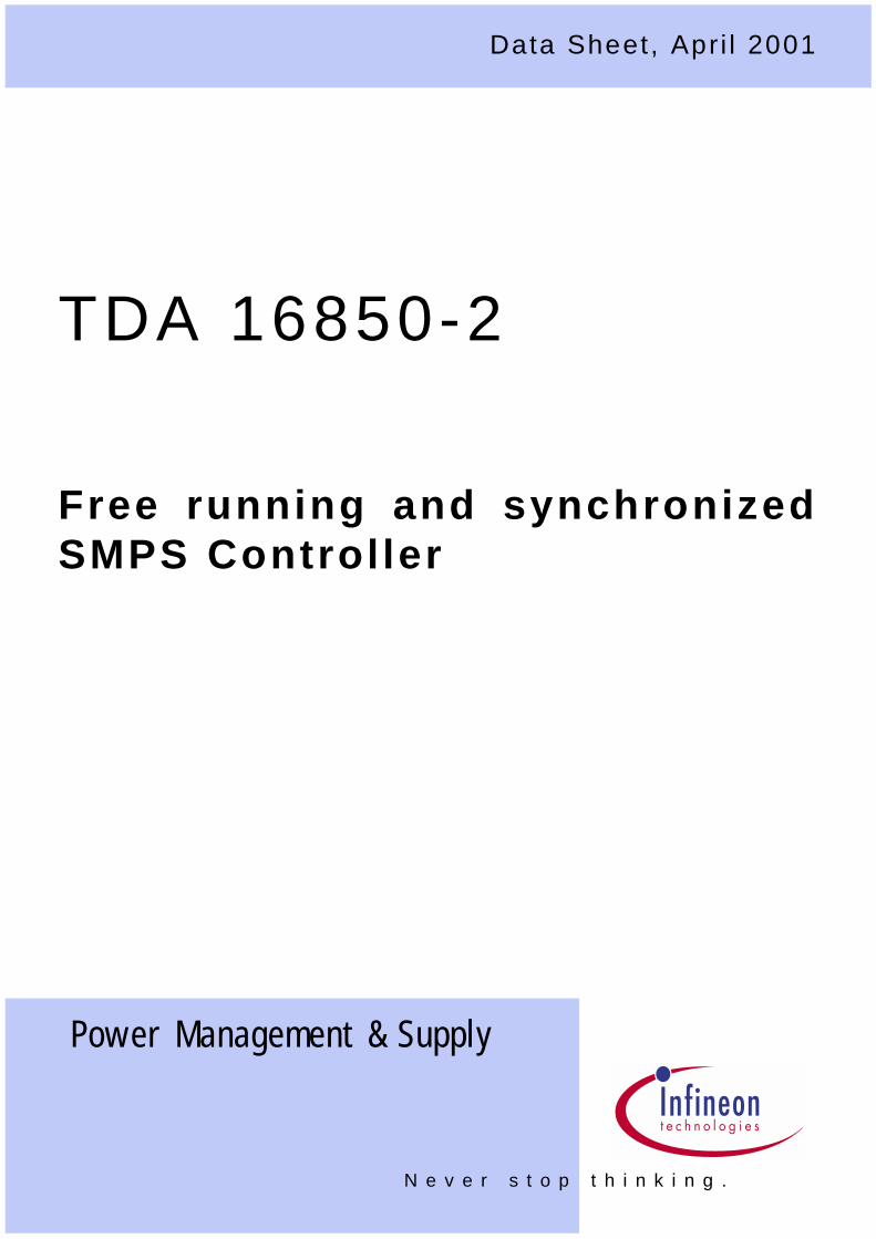
Synchronized SMPS Controller
Type Ordering Code Package
TDA16850-2 Q67040-S4404-A P-DIP-8
TDA 16850-2
AC 90V - 270V
Standby
GATE
GND
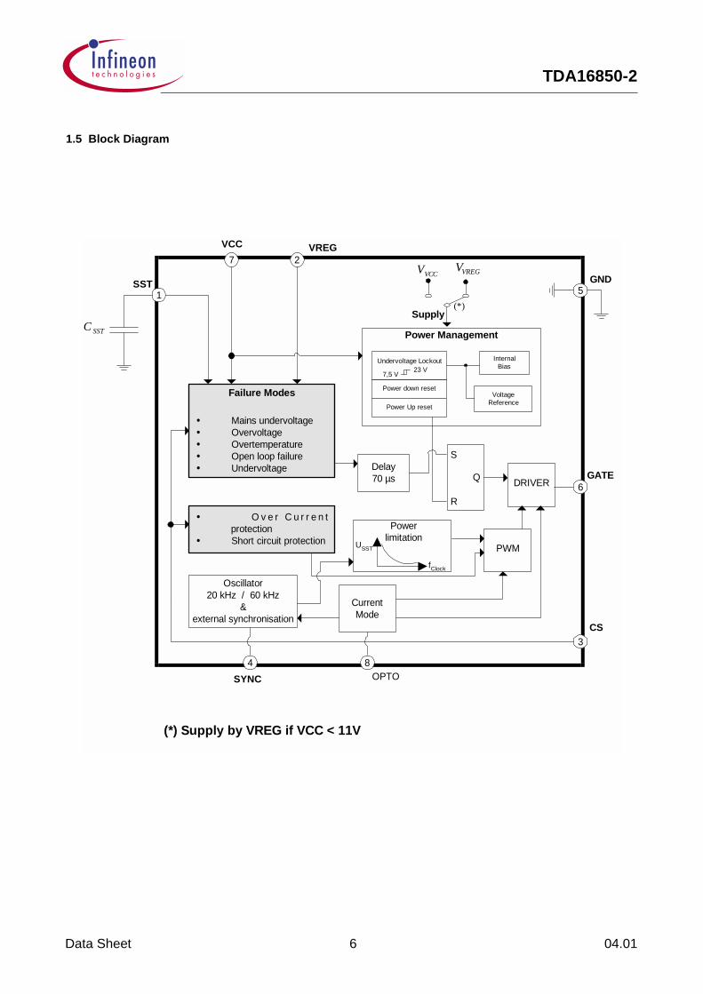
Failure Modes
Mains undervoltage Overvoltage Overtemperature Open loop failure Undervoltage
Over Current protection Short circuit protection
Oscillator20 kHz / 60 kHz
&external synchronisation
Delay70 µs
PWM
CurrentMode
DRIVER
US ST
fClock
Powerlimitation
S
R
Q
Supply
VCCV VREGV
(*)
Power Management
InternalBias
Power down reset
Power Up reset
Undervoltage Lockout23 V
7,5 V
VoltageReference
6
3
84
27
51
VCC
SST
CS
OPTOSYNC
VREG
SSTC
optoR
senseR
ConverterDC O utput
Feedback
Fee
dba
ck
(*) Supply by VREG if VCC < 11V
Product Highlights
• Synchronisation range 30 kHz to 130 kHz• Maximum output power independant of frequency• Standby mode with reduced output voltage by factor 5• Mode changing and voltage feedback through only
one optocoupler• Off mode with power consumption less than 250 mW• Standby mode with power consumption less than 1W• Without synchronisation operation with internal
oscillator 20kHz/60kHz• Different failure modes recognition with latch function• Minimum external circuitry
Typical application
TDA16850-2
Data Sheet 3 04.01
Table of contents
1Overview . . . . . . . . . . . . . . . . . . . . . . . . . . . . . . . . . . . . . . . . . . . . . . . . . . . . . . . . . . .51.1 Features . . . . . . . . . . . . . . . . . . . . . . . . . . . . . . . . . . . . . . . . . . . . . . . . . . .51.2 Special Features . . . . . . . . . . . . . . . . . . . . . . . . . . . . . . . . . . . . . . . . . . . . .51.3 Protection Features . . . . . . . . . . . . . . . . . . . . . . . . . . . . . . . . . . . . . . . . . . .51.4 General Remarks . . . . . . . . . . . . . . . . . . . . . . . . . . . . . . . . . . . . . . . . . . . .51.5 Block Diagram . . . . . . . . . . . . . . . . . . . . . . . . . . . . . . . . . . . . . . . . . . . . . . .61.6 Pin Connection and Description . . . . . . . . . . . . . . . . . . . . . . . . . . . . . . . . .7
2Functional Description . . . . . . . . . . . . . . . . . . . . . . . . . . . . . . . . . . . . . . . . . . . . . . .82.1 Off mode / Switch on process . . . . . . . . . . . . . . . . . . . . . . . . . . . . . . . . . .102.2 Startup Mode . . . . . . . . . . . . . . . . . . . . . . . . . . . . . . . . . . . . . . . . . . . . . . .102.3 Normal Mode . . . . . . . . . . . . . . . . . . . . . . . . . . . . . . . . . . . . . . . . . . . . . . .102.4 Standby Mode . . . . . . . . . . . . . . . . . . . . . . . . . . . . . . . . . . . . . . . . . . . . . .102.5 Power down Mode . . . . . . . . . . . . . . . . . . . . . . . . . . . . . . . . . . . . . . . . . . .102.6 Protection Mode . . . . . . . . . . . . . . . . . . . . . . . . . . . . . . . . . . . . . . . . . . . .102.7 Protection Circuitry . . . . . . . . . . . . . . . . . . . . . . . . . . . . . . . . . . . . . . . . . .102.7.1 Over Current . . . . . . . . . . . . . . . . . . . . . . . . . . . . . . . . . . . . . . . . . . . . . . .102.7.2 Short Circuit . . . . . . . . . . . . . . . . . . . . . . . . . . . . . . . . . . . . . . . . . . . . . . . .102.7.3 Failure Modes . . . . . . . . . . . . . . . . . . . . . . . . . . . . . . . . . . . . . . . . . . . . . .102.7.3.1 Mains Undervoltage . . . . . . . . . . . . . . . . . . . . . . . . . . . . . . . . . . . . . . . . .102.7.3.2 IC Supply Overvoltage . . . . . . . . . . . . . . . . . . . . . . . . . . . . . . . . . . . . . . .102.7.3.3 IC Overtemperature . . . . . . . . . . . . . . . . . . . . . . . . . . . . . . . . . . . . . . . . .102.7.3.4 VREG Loop Failure . . . . . . . . . . . . . . . . . . . . . . . . . . . . . . . . . . . . . . . . .102.7.3.5 IC SupplyUndervoltage . . . . . . . . . . . . . . . . . . . . . . . . . . . . . . . . . . . . . . .10
3Functional Block Description . . . . . . . . . . . . . . . . . . . . . . . . . . . . . . . . . . . . . . . . .113.1 VCC and VREG Section . . . . . . . . . . . . . . . . . . . . . . . . . . . . . . . . . . . . . .123.2 OPTO Section . . . . . . . . . . . . . . . . . . . . . . . . . . . . . . . . . . . . . . . . . . . . . .123.3 Oscillator and Synchronization . . . . . . . . . . . . . . . . . . . . . . . . . . . . . . . . .123.4 PWM Section . . . . . . . . . . . . . . . . . . . . . . . . . . . . . . . . . . . . . . . . . . . . . . .133.5 Current Sense Section . . . . . . . . . . . . . . . . . . . . . . . . . . . . . . . . . . . . . . .143.6 Soft Start . . . . . . . . . . . . . . . . . . . . . . . . . . . . . . . . . . . . . . . . . . . . . . . . . .143.7 Output Power Limiting . . . . . . . . . . . . . . . . . . . . . . . . . . . . . . . . . . . . . . . .143.8 GATE Driver . . . . . . . . . . . . . . . . . . . . . . . . . . . . . . . . . . . . . . . . . . . . . . .143.9 Protection Circuitry . . . . . . . . . . . . . . . . . . . . . . . . . . . . . . . . . . . . . . . . . .153.9.1 Over Current . . . . . . . . . . . . . . . . . . . . . . . . . . . . . . . . . . . . . . . . . . . . . . .153.9.2 Short Circuit . . . . . . . . . . . . . . . . . . . . . . . . . . . . . . . . . . . . . . . . . . . . . . .153.9.3 Failure Modes . . . . . . . . . . . . . . . . . . . . . . . . . . . . . . . . . . . . . . . . . . . . . .153.9.3.1 Mains Undervoltage . . . . . . . . . . . . . . . . . . . . . . . . . . . . . . . . . . . . . . . . .153.9.3.2 IC Supply Overvoltage . . . . . . . . . . . . . . . . . . . . . . . . . . . . . . . . . . . . . . .153.9.3.3 IC Overtemperature . . . . . . . . . . . . . . . . . . . . . . . . . . . . . . . . . . . . . . . . .153.9.3.4 VREG Loop Failure . . . . . . . . . . . . . . . . . . . . . . . . . . . . . . . . . . . . . . . . .15
TDA16850-2
Data Sheet 4 04.01
3.9.3.5 IC Supply Undervoltage . . . . . . . . . . . . . . . . . . . . . . . . . . . . . . . . . . . . .15
4Electrical Characteristics . . . . . . . . . . . . . . . . . . . . . . . . . . . . . . . . . . . . . . . . . . . .164.1 Absolute Maximum Ratings . . . . . . . . . . . . . . . . . . . . . . . . . . . . . . . . . . . .164.2 Operating Range . . . . . . . . . . . . . . . . . . . . . . . . . . . . . . . . . . . . . . . . . . . .174.3 Characteristics . . . . . . . . . . . . . . . . . . . . . . . . . . . . . . . . . . . . . . . . . . . . . .18
5Application Circuits . . . . . . . . . . . . . . . . . . . . . . . . . . . . . . . . . . . . . . . . . . . . . . . . .235.1 Application Circuit 1. See Description 5.3.1 . . . . . . . . . . . . . . . . . . . . . . .235.2 Application Circuit 2. See Decription 5.3.2 . . . . . . . . . . . . . . . . . . . . . . . .245.3 Description of Application Circuits . . . . . . . . . . . . . . . . . . . . . . . . . . . . . . .255.3.1 Application Circuit 1 . . . . . . . . . . . . . . . . . . . . . . . . . . . . . . . . . . . . . . . . .255.3.2 Application Circuit 2 . . . . . . . . . . . . . . . . . . . . . . . . . . . . . . . . . . . . . . . . .25
Data Sheet 5 04.01
Synchronized SMPS Controller
As far as patents or other rights of third parties are concerned, liability is only assumed for components, not forapplications, processes and circuits implemented within components or assemblies.The information describes the type of component and shall not be considered as assured characteristics.
Type Ordering Code Package
TDA16850-2 Q67040-S4404-A P-DIP-8
TDA 16850-2
1 Overview
1.1 Features
– Controller for Flyback Topology– Current mode PWM with shunt resistor and spike
blanking– Leading edge triggered pulse width modulation– Fast, soft switching totem pole gate drive (1 A)– Soft start management for safe start up
1.2 Special Features
– Typical 100 µA start-up supply current– Low quiescent current (5 mA)– Maximum output power independent of frequency– 20 kHz internal oscillator for start-up and standby
mode– 60 kHz internal oscillator for non synchronized
normal mode– Synchronization range 30 kHz to 130 kHz– Feedback via optocoupler in normal operation– Feedback via transformer winding in standby mode– Standby mode with reduced output voltages by
factor of 5– Off mode with power consumption less then 1 W– Mode switching and voltage feedback through only
one optocoupler– Different failure modes recognition with latch
function
1.3 Protection Features
– Fast and slow peak current limitation– Mains undervoltage protection – IC Supply Overvoltage– IC Supply Undervoltage– Loop Failure– Over temperature switch off– Over current protection– Short circuit protection
1.4 General Remarks
The TDA 16850-2 comprises the complete control forflyback switched mode power supplies especially inCRT monitors. It also performs all necessary protectionfunctions in flyback converters. The TDA 16850-2applies to converters with input line voltages rangingfrom 90 VAC to 270 VAC .The maximum duty cycle depends on frequency, linevoltage and soft start management. The maximumoutput power therefore will be limited effectively in caseof a secondary overload.All clock signals as well as the PWM voltage ramp areeither synchronized by the internal oscillator or by thesynchronisation signal at pin SYNC. The internaloscillator is activated if there is no signal at SYNC. Anhorizontal deflection signal at pin SYNC synchronizesthe internal oscillator automatically.Mode switching is done via the input current at pinOPTO. In the standby mode the TDA 16850-2 gets itssupply from pin VREG. The voltage at VREG is thenalso the feedback voltage. The TDA 16850-2 will switchoff the power supply and enter the off mode when theoptocoupler current is completely turned off. It can restart from a short optocoupler current pulse,which can be derived from a vertical synchronizationpulse. The TDA 16850-2 operates in the normal mode ifVVCC and I OPTO are in their nominal range.
TDA16850-2
Data Sheet 6 04.01
GATE
GND
Failure Modes
Mains undervoltage Overvoltage Overtemperature Open loop failure Undervoltage
O v e r C u r r e n tprotection
Short circuit protection
Oscillator20 kHz / 60 kHz
&external synchronisation
Delay70 µs
PWM
CurrentMode
DRIVER
USST
fClock
Powerlimitation
S
R
Q
Supply
VCCV VREGV
(*)
Power Management
InternalBias
Power down reset
Power Up reset
Undervoltage Lockout23 V
7,5 V
VoltageReference
6
3
84
27
51
VCC
SST
CS
OPTOSYNC
VREG
SSTC
(*) Supply by VREG if VCC < 11V
1.5 Block Diagram
TDA16850-2
Data Sheet 7 04.01
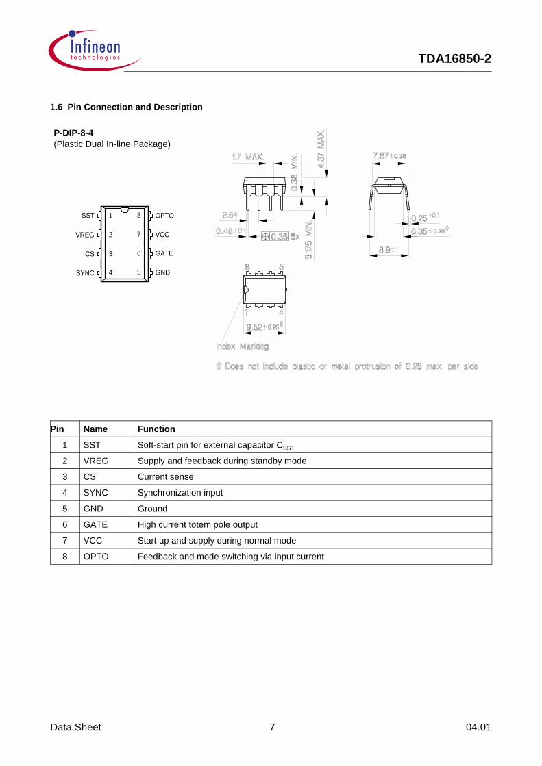
1.6 Pin Connection and Description
Pin Name Function
1 SST Soft-start pin for external capacitor CSST
2 VREG Supply and feedback during standby mode
3 CS Current sense
4 SYNC Synchronization input
5 GND Ground
6 GATE High current totem pole output
7 VCC Start up and supply during normal mode
8 OPTO Feedback and mode switching via input current
SYNC
CS
VREG
SST
GND
GATE
VCC
OPTO1
2
3
4
8
7
6
5
P-DIP-8-4(Plastic Dual In-line Package)
TDA16850-2
Data Sheet 8 04.01
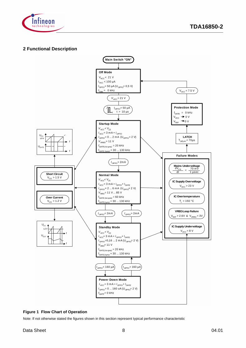
2 Functional Description
Figure 1 Flow Chart of Operation
Note: If not otherwise stated the figures shown in this section represent typical performance characteristic
LATCHTDELAY = 70µs
VVCC < 7.5 V
Startup Mode VVCC < VZ1
IVCC = 3 m A + IOPTO
IOPTO = 0 ... 2 m A (UOPTO = 2 V) VVREG = 11 V fGATE (no sync) = 20 kHz fGATE (sync) = 30 ... 130 kHz
Standby Mode VVCC < VZ1
IVCC= 3 m A + IOPTO + IGATE
IOPTO =0,16 ... 2 m A (UOPTO= 2 V) VREG= 11 V fGATE (no sync) = 20 kHz fGATE (sync) = 30 ... 130 kHz
Off Mode VVCC < 21 V IVCC < 100 µA IOPTO < 50 µA (UOPTO= 0,5 V) fGate = 0 kHz
Normal Mode VVCC< VZ1
IVCC = 3 m A + IOPTO + IGATE
IOPTO = 2 ... 6 m A (UOPTO= 2 V) VREG = 11 V ... 85 V fGATE (no sync) = 60 kHz fGATE (sync) = 30 ... 130 kHz
VVCC > 21 V
IOPTO > 2mA
Power Down Mode IVCC = 3 m A + IOPTO + IGATE
IOPTO = 0 ... 160 uA (UOPTO= 2 V) fGATE = 0 kHz
IOPTO > 160 µA
IOPTO < 2m A
IOPTO < 160 µA
t > 10 µsIOPTO > 50 µA
t
I
Main Switch "ON"
UCS
1.2 V
USST
t
t
Over CurrentVCS > 1.2 V
Short CircuitVCS > 1.5 V
IOPTO > 2mA
UCS1.5 V
UGATE
t
t
Protection Mode fGATE = 0 kHz VVCC 0 V VSST 0 V
Failure Modes
IC OvertemperatureTj > 150 °C
IC Supply OvervoltageVVCC > 23 V
VREG Loop FailureVSST > 2.6V & VVREG < 3V
Mains UndervoltagedVCS
dt 70 mV1 µsec<
IC Supply UndervoltageVVCC < 8 V
TDA16850-2
Data Sheet 9 04.01
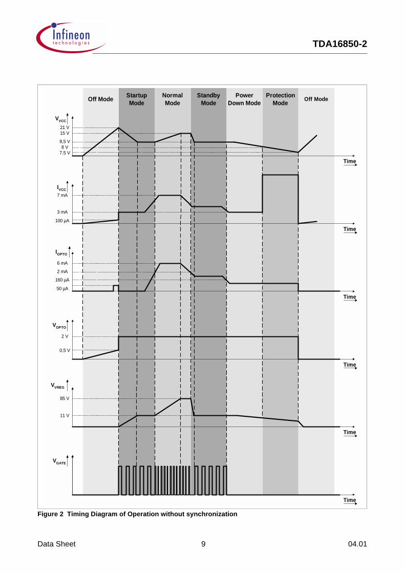
Figure 2 Timing Diagram of Operation without synchronization
VOPTO
VVCC
IOPTO
50 µA
Off ModeStartupMode
160 µA
2 mA
21 V
NormalMode
StandbyMode
6 mA
PowerDown Mode
15 V
8 V7.5 V
ProtectionMode
Off Mode
0,5 V
2 V
IVCC
100 µA
3 mA
7 mA
VGATE
VVREG
11 V
85 V
Time
9,5 V
Time
Time
Time
Time
Time
Data Sheet 10 04.01
TDA16850-2
(see Figure 1, Page4 and Figure 2, Page 5)
2.1 Off mode / Switch on process
At first the chip is in off mode. During switch on processthe supply voltage at VCC increases from 0 V to theswitch on threshold of VVCC. The total currentconsumption of TDA 16850-2 is typ.100 µA in this case.When VVCC exceeds the voltage of 21 V the chip can beactivated by an optocoupler current pulse higher than50 µA (typ.) and 10 µs (typ.) duration.
2.2 Startup Mode
Entering startup mode the internal supply of TDA16850-2 is switched on and all blocks are operable. Inthe startup mode a current out of pin OPTO of 0 µA <|IOPTO| < 2 mA is allowed. If there is no signal at pinSYNC, the TDA 16850-2 generates gate pulses at arate of 20 kHz (typ.). The pulse width is first increasedduring a soft start and then regulated for 11 V voltageat Pin VREG.
2.3 Normal Mode
Normal mode can be entered from startup mode orstandby mode by increasing the opto current above 2mA (typ.). In the normal mode the supply voltage mustbe 8 V < VVCC < 23 V typ. When there is no signalpresent at SYNC, GATE clocks with a frequency oftypical fOSC = 60 kHz (typ.). If there is a signal at SYNCof 30 kHz < fOSC < 130kHz the internal oscillator issynchronized automatically with this signal. If theVREG voltage is higher than 11 V, the output pulsewidth depends on the opto current. A higher optocurrent means wider output pulses and a higher outputpower of the power supply. Duty cycle minimum will beachieved at a OPTO current of 2 mA (typ.).
2.4 Standby Mode
Standby mode is reached from either normal mode orpower down mode by adjusting the opto current within160 µA to 2 mA. Voltage VVREG will then be regulated to typ. 11 V. TheOscillator frequency in standby mode is typ. 20 kHz. Asignal at pin SYNC is also evaluated in standby modeand the oscillator is synchronized accordingly.Standby mode can be quit to move to normal mode,power down mode, or to move to protection mode.In the standby mode the supply to the chip can beswitched over from pin VCC to pin VREG. The switchis a current limiting switching transistor. It’s switched onwhen VVCC drops below typ. 10 V in normal mode.When VVREG is greater than VVCC the chip is nowsupplied via VVREG. At the same time the internal controlof the duty cycle at GATE is set so that there is typicallya voltage of 11 V at pin VREG. At VCC there is then avoltage of typ. 9.5 V. The current at pin OPTO muststay between 160 µA < |IOPTO| < 2 mA.
2.5 Power down Mode
At power down mode GATE will be disabled. Thepower down mode is entered when the OPTO inputcurrent is less than 160 µA (typ.), after the IC has beenin the normal mode before.
2.6 Protection Mode
All failure modes will disable GATE. This is theprotection mode, which is latched and VCC and SSTwill be discharged by internal transistors. Protectionmode can only be left through the off mode if VVCC isbelow 7.5 V (typ.).
2.7 Protection Circuitry
2.7.1 Over Current
The voltage at pin CS will be sensed by a comparator.Until the voltage at pin CS is more than 1,2V (typ.) theduty cycle will be reduced by discharging Pin SST by ainternal transistor.
2.7.2 Short Circuit
In case of a secondary short circuit, GATE will bedisabled as long as the voltage at pin CS is more than1,5 V (typ.).
2.7.3 Failure Modes
The error message of the failure functions are stored ina latch after a delay of typ. 70 µs. GATE then will bedisabled. The latch is reset again when the chip is in offmode .
2.7.3.1 Mains Undervoltage
A circuit checks the rise of the ramp singal at pin CSfor minimum slew rate.
2.7.3.2 IC Supply Overvoltage
A circuit checks the voltage at pin VCC.
2.7.3.3 IC Overtemperature
A thermal probe checks the temperature of the chip.
2.7.3.4 VREG Loop Failure
A circuit checks if the voltage at VREG is below 3 V(typ.) and the voltage at pin SST have reached 2,6V(typ.).
2.7.3.5 IC SupplyUndervoltage
A comparator checks the voltage at VCC.
TDA16850-2
Data Sheet 11 04.01
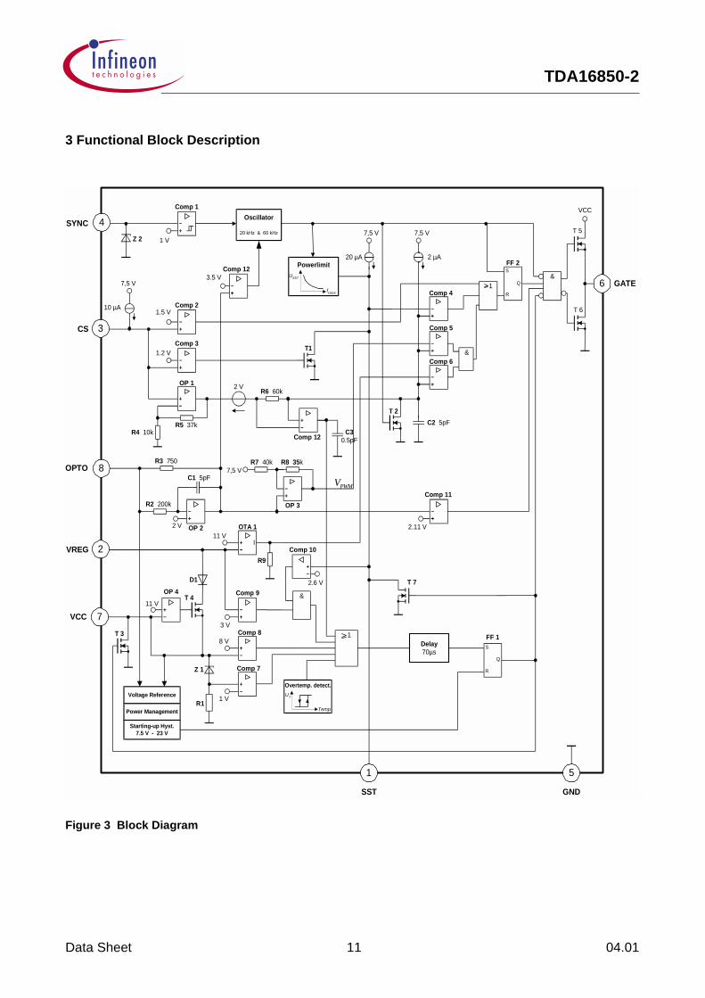
3 Functional Block Description
Figure 3 Block Diagram
GATE
OPTO
Oscillator
20 kHz & 60 kHz
SST
8 V
2 V
&
1R
S
Q&
R
S
Q
2
4
7
8
11 V
&
20 µA
3
10 µA1.5 V
Comp 2
1.2 VComp 3
OP 1
R3 750
OP 2
Comp 11
Comp 4
3 V
Comp 10
2.6 V
R1
Z 1 Comp 7
Comp 8
T1
Overtemp. detect.
Temp
UT
1 5
VCC
6
FF 2
FF 1
1 V
Comp 1
USST
fClock
Powerlimit
T 2
Delay70µs
1 V
T 3
T 5
T 6
1
7,5 V
7,5 V
2 V
I
OTA 1
Comp 12
Z 2
11 V
OP 4T 4
D1
Comp 6
Comp 5
GND
SYNC
CS
VREG
VCC
Starting-up Hyst.7.5 V - 23 V
Voltage Reference
Power Management
R9
Comp 9T 7
R2 200k
C1 5pF
R5 37kR4 10k
R6 60k
7,5 V
2 µA
C2 5pFC3
0.5pF
2.11 V
Comp 123.5 V
OP 3
R8 35k7,5 V
R7 40k
PWMV
Data Sheet 12 04.01
TDA16850-2
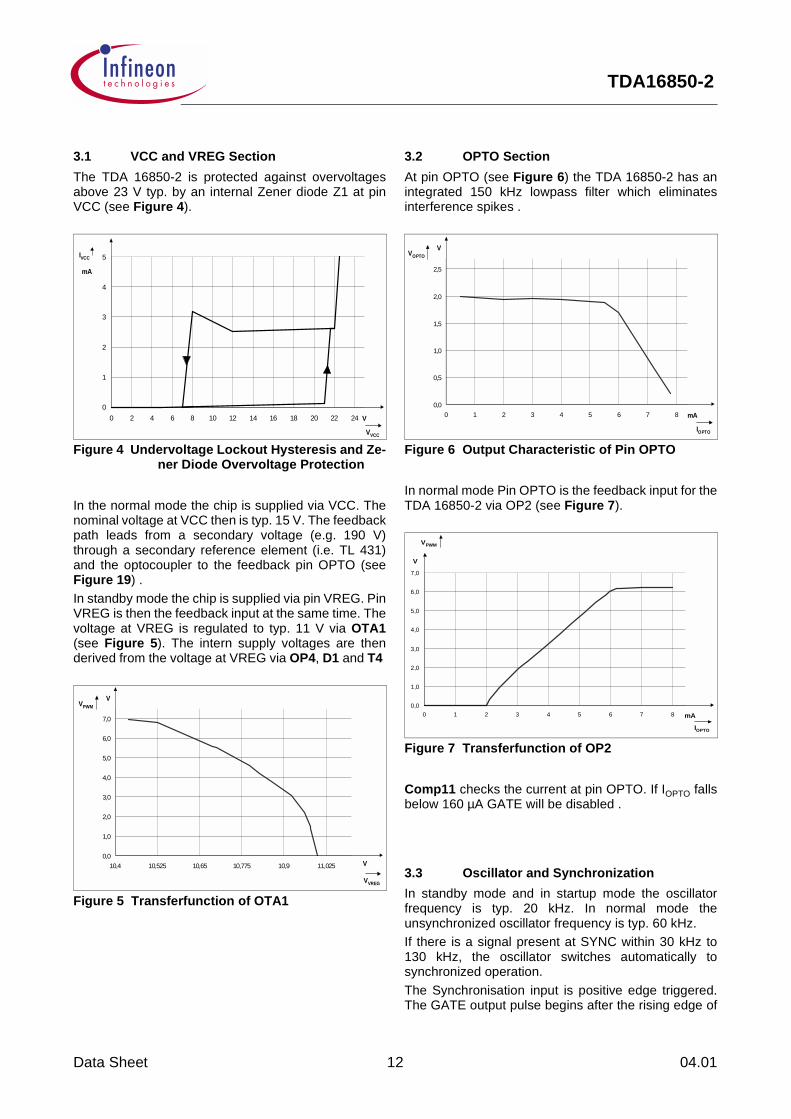
3.1 VCC and VREG Section
The TDA 16850-2 is protected against overvoltagesabove 23 V typ. by an internal Zener diode Z1 at pinVCC (see Figure 4).
Figure 4 Undervoltage Lockout Hysteresis and Ze-ner Diode Overvoltage Protection
In the normal mode the chip is supplied via VCC. Thenominal voltage at VCC then is typ. 15 V. The feedbackpath leads from a secondary voltage (e.g. 190 V)through a secondary reference element (i.e. TL 431)and the optocoupler to the feedback pin OPTO (seeFigure 19) . In standby mode the chip is supplied via pin VREG. PinVREG is then the feedback input at the same time. Thevoltage at VREG is regulated to typ. 11 V via OTA1(see Figure 5). The intern supply voltages are thenderived from the voltage at VREG via OP4, D1 and T4
Figure 5 Transferfunction of OTA1
3.2 OPTO Section
At pin OPTO (see Figure 6) the TDA 16850-2 has anintegrated 150 kHz lowpass filter which eliminatesinterference spikes .
Figure 6 Output Characteristic of Pin OPTO
In normal mode Pin OPTO is the feedback input for theTDA 16850-2 via OP2 (see Figure 7).
Figure 7 Transferfunction of OP2
Comp11 checks the current at pin OPTO. If IOPTO fallsbelow 160 µA GATE will be disabled .
3.3 Oscillator and Synchronization
In standby mode and in startup mode the oscillatorfrequency is typ. 20 kHz. In normal mode theunsynchronized oscillator frequency is typ. 60 kHz. If there is a signal present at SYNC within 30 kHz to130 kHz, the oscillator switches automatically tosynchronized operation.The Synchronisation input is positive edge triggered.The GATE output pulse begins after the rising edge of
0
1
2
3
4
5
0 2 4 6 8 10 12 14 16 18 20 22 24 V
VVCC
mA
IVCC
0,0
1,0
2,0
3,0
4,0
5,0
6,0
7,0
10,4 10,525 10,65 10,775 10,9 11,025 V
VVREG
VVPWM
0,0
0,5
1,0
1,5
2,0
2,5
0 1 2 3 4 5 6 7 8 mA
IOPTO
VVOPTO
0,0
1,0
2,0
3,0
4,0
5,0
6,0
7,0
0 1 2 3 4 5 6 7 8 mA
IOPTO
V
VPWM
Data Sheet 13 04.01
TDA16850-2
the SYNC signal with a delay, which is 1/20 of theSYNC signal period (see Figure 8).
Figure 8 Timing Diagram Oscillator with Synchro-nisation
Figure 9 Timing Diagram 60/20 kHz Switch and Synchronisation
If IOPTO falls below 2 mA the unsynchronized oscillatorwill switch from 60 kHz to 20 kHz (see Figure 9).The sync input is protected by a Zener diode Z2 and ahysteresis comparator Comp1.
3.4 PWM Section
The PWM Section is equipped with improved currentmode control. The pulse width modulator of the TDA 16850-2operates at a small pulse width in voltage mode andwith a larger pulse width in current mode. The GATEpuls depends on the SST voltage via Comp4, theOPTO current via Comp5 and the VREG voltage viaComp6. A voltage at VREG lower than 11 V will lead tolong GATE pulses, as well as a high OPTO current. Alow voltage at SST dominates over the OPTO andVREG conditions and sets the limit for the maximumGATE pulse width. The input, which generates thelonger GATE pulses will dominate over the input, whichwould generate the shorter Gate pulses (see Figure10).
Figure 10 Timing Diagram PWM Section
VCOMP1
VOSC
VGATE
Time
Time
Time
VSYNC
Time
IOPTO
2 mA
VOSC
VSYNC
Time
Time
Time
VOSC
VGATE
VCS
VRMP
Time
Time
Time
Time
VPWM OFF
VPWM
ON
Data Sheet 14 04.01
TDA16850-2
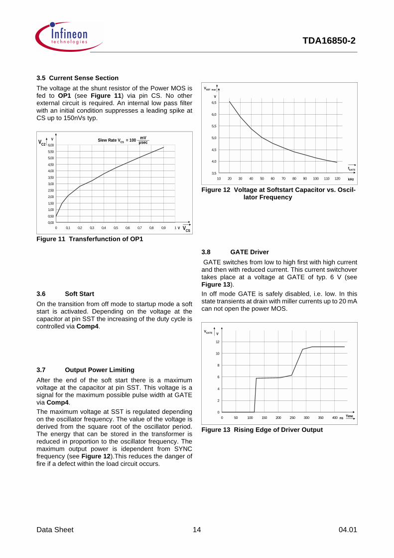
3.5 Current Sense Section
The voltage at the shunt resistor of the Power MOS isfed to OP1 (see Figure 11) via pin CS. No otherexternal circuit is required. An internal low pass filterwith an initial condition suppresses a leading spike atCS up to 150nVs typ.
Figure 11 Transferfunction of OP1
3.6 Soft Start
On the transition from off mode to startup mode a softstart is activated. Depending on the voltage at thecapacitor at pin SST the increasing of the duty cycle iscontrolled via Comp4.
3.7 Output Power Limiting
After the end of the soft start there is a maximumvoltage at the capacitor at pin SST. This voltage is asignal for the maximum possible pulse width at GATEvia Comp4.The maximum voltage at SST is regulated dependingon the oscillator frequency. The value of the voltage isderived from the square root of the oscillator period.The energy that can be stored in the transformer isreduced in proportion to the oscillator frequency. Themaximum output power is idependent from SYNCfrequency (see Figure 12).This reduces the danger offire if a defect within the load circuit occurs.
Figure 12 Voltage at Softstart Capacitor vs. Oscil-lator Frequency
3.8 GATE Driver
GATE switches from low to high first with high currentand then with reduced current. This current switchovertakes place at a voltage at GATE of typ. 6 V (seeFigure 13). In off mode GATE is safely disabled, i.e. low. In thisstate transients at drain with miller currents up to 20 mAcan not open the power MOS.
Figure 13 Rising Edge of Driver Output
0,00
0,50
1,00
1,50
2,00
2,50
3,00
3,50
4,00
4,50
5,00
5,50
6,00
0 0,1 0,2 0,3 0,4 0,5 0,6 0,7 0,8 0,9 1 V VCS
VVC2Slew Rate VCS = 100 mV
µsec
3,5
4,0
4,5
5,0
5,5
6,0
6,5
10 20 30 40 50 60 70 80 90 100 110 120 kHz
fGATE
V
VSST max
0
2
4
6
8
10
12
0 50 100 150 200 250 300 350 400 Time
VGATE
ns
V
Data Sheet 15 04.01
TDA16850-2
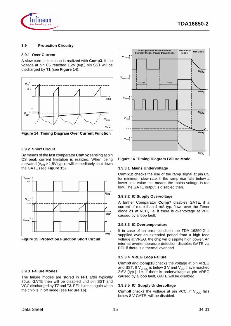
3.9 Protection Circuitry
3.9.1 Over Current
A slow current limitation is realized with Comp3. If thevoltage at pin CS reached 1,2V (typ.) pin SST will bedischarged by T1 (see Figure 14).
Figure 14 Timing Diagram Over Current Function
3.9.2 Short Circuit
By means of the fast comparator Comp2 sensing at pinCS peak current limitation is realized. When beingactivated (VCS > 1,5V typ.) it will immediately shut downthe GATE (see Figure 15).
Figure 15 Protection Function Short Circuit
3.9.3 Failure Modes
The failure modes are stored in FF1 after typically70µs. GATE then will be disabled und pin SST andVCC discharged by T7 and T3. FF1 is reset again whenthe chip is in off mode (see Figure 16).
Figure 16 Timing Diagram Failure Mode
3.9.3.1 Mains Undervoltage
Comp12 checks the rise of the ramp signal at pin CSfor minimum slew rate. If the ramp rise falls below alower limit value this means the mains voltage is toolow. The GATE output is disabled then.
3.9.3.2 IC Supply Overvoltage
A further Comparator Comp7 disables GATE, if acurrent of more than 4 mA typ. flows over the Zenerdiode Z1 at VCC, i.e. if there is overvoltage at VCCcaused by a loop fault.
3.9.3.3 IC Overtemperature
If in case of an error condition the TDA 16850-2 issupplied over an extended period from a high feedvoltage at VREG, the chip will dissipate high power. Aninternal overtemperature detection disables GATE viaFF1 if there is a thermal overload.
3.9.3.4 VREG Loop Failure
Comp9 and Comp10 checks the voltage at pin VREGand SST. If VVREG is below 3 V and VSST have reached2,6V (typ.), i.e. if there is undervoltage at pin VREGcaused by a loop fault, GATE will be disabled.
3.9.3.5 IC Supply Undervoltage
Comp8 checks the voltage at pin VCC. If VVCC fallsbelow 8 V GATE will be disabled.
VSST
VCS
1,2 V
Time
Time
VRMP
VGATE
Time
Time
VCS
1,5 V
VPWM
out
Time
VFailure
VLatch out
VGATE
VVCC
VSST
7.5 V
T < 70µs
Startup Mode, Normal Mode,Standby Mode, Power Down Mode
ProtectionMode Off Mode
T > 70µs
Time
Time
Time
Time
Time
TDA16850-2
Data Sheet 16 04.01
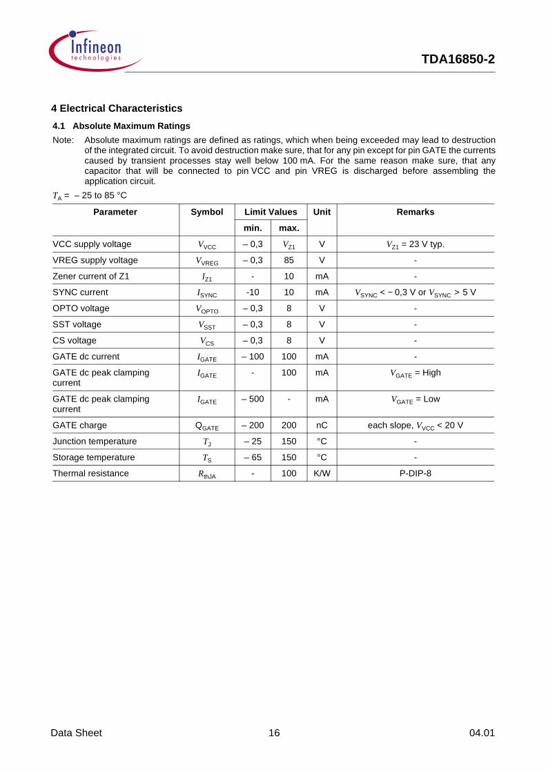
4 Electrical Characteristics
4.1 Absolute Maximum Ratings
Note: Absolute maximum ratings are defined as ratings, which when being exceeded may lead to destructionof the integrated circuit. To avoid destruction make sure, that for any pin except for pin GATE the currentscaused by transient processes stay well below 100 mA. For the same reason make sure, that anycapacitor that will be connected to pin VCC and pin VREG is discharged before assembling theapplication circuit.
TA = – 25 to 85 °C
Parameter Symbol Limit Values Unit Remarks
min. max.
VCC supply voltage VVCC – 0,3 VZ1 V VZ1 = 23 V typ.
VREG supply voltage VVREG – 0,3 85 V -
Zener current of Z1 IZ1 - 10 mA -
SYNC current ISYNC -10 10 mA VSYNC < −=0,3 V or VSYNC >===5 V
OPTO voltage VOPTO – 0,3 8 V -
SST voltage VSST – 0,3 8 V -
CS voltage VCS – 0,3 8 V -
GATE dc current IGATE – 100 100 mA -
GATE dc peak clamping current
IGATE - 100 mA VGATE = High
GATE dc peak clamping current
IGATE – 500 - mA VGATE = Low
GATE charge QGATE – 200 200 nC each slope, VVCC < 20 V
Junction temperature TJ – 25 150 °C -
Storage temperature TS – 65 150 °C -
Thermal resistance RthJA - 100 K/W P-DIP-8
TDA16850-2
Data Sheet 17 04.01
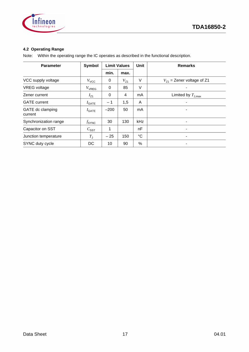
4.2 Operating Range
Note: Within the operating range the IC operates as described in the functional description.
Parameter Symbol Limit Values Unit Remarks
min. max.
VCC supply voltage VVCC 0 VZ1 V VZ1 = Zener voltage of Z1
VREG voltage VVREG 0 85 V -
Zener current IZ1 0 4 mA Limited by TJ,max
GATE current IGATE – 1 1,5 A -
GATE dc clampingcurrent
IGATE –200 50 mA -
Synchronization range fSYNC 30 130 kHz -
Capacitor on SST CSST 1 nF -
Junction temperature TJ – 25 150 °C -
SYNC duty cycle DC 10 90 % -
TDA16850-2
Data Sheet 18 04.01
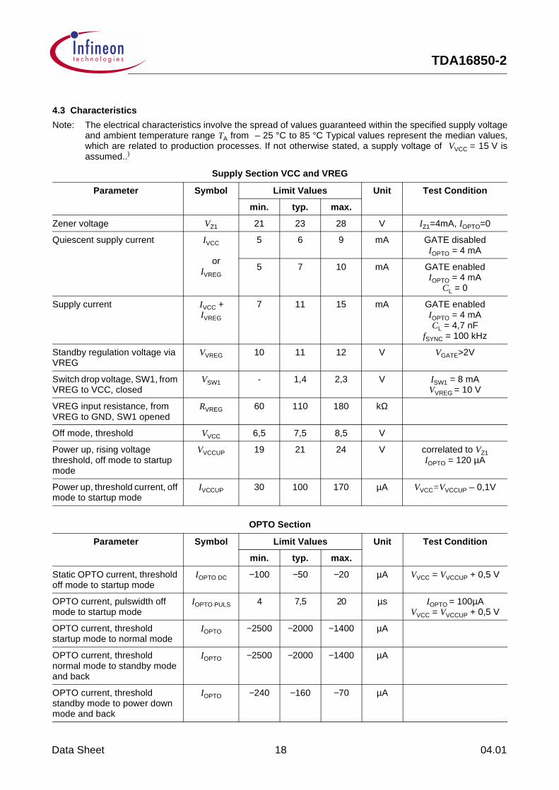
4.3 Characteristics
Note: The electrical characteristics involve the spread of values guaranteed within the specified supply voltageand ambient temperature range TA from – 25 °C to 85 °C Typical values represent the median values,which are related to production processes. If not otherwise stated, a supply voltage of VVCC = 15 V isassumed..)
Supply Section VCC and VREG
Parameter Symbol Limit Values Unit Test Condition
min. typ. max.
Zener voltage VZ1 21 23 28 V IZ1=4mA, IOPTO=0
Quiescent supply current IVCC
orIVREG
5 6 9 mA GATE disabledIOPTO = 4 mA
5 7 10 mA GATE enabledIOPTO = 4 mA
CL = 0
Supply current IVCC +IVREG
7 11 15 mA GATE enabledIOPTO = 4 mACL = 4,7 nF
fSYNC = 100 kHz
Standby regulation voltage via VREG
VVREG 10 11 12 V VGATE>2V
Switch drop voltage, SW1, from VREG to VCC, closed
VSW1 - 1,4 2,3 V ISW1 = 8 mAVVREG = 10 V
VREG input resistance, from VREG to GND, SW1 opened
RVREG 60 110 180 kΩ
Off mode, threshold VVCC 6,5 7,5 8,5 V
Power up, rising voltage threshold, off mode to startup mode
VVCCUP 19 21 24 V correlated to VZ1IOPTO = 120 µA
Power up, threshold current, off mode to startup mode
IVCCUP 30 100 170 µA VVCC=VVCCUP – 0,1V
OPTO Section
Parameter Symbol Limit Values Unit Test Condition
min. typ. max.
Static OPTO current, threshold off mode to startup mode
IOPTO DC −100 −50 −20 µA VVCC = VVCCUP + 0,5 V
OPTO current, pulswidth off mode to startup mode
IOPTO PULS 4 7,5 20 µs IOPTO = 100µAVVCC = VVCCUP + 0,5 V
OPTO current, threshold startup mode to normal mode
IOPTO −2500 −2000 −1400 µA
OPTO current, threshold normal mode to standby mode and back
IOPTO −2500 −2000 −1400 µA
OPTO current, threshold standby mode to power down mode and back
IOPTO −240 −160 −70 µA
TDA16850-2
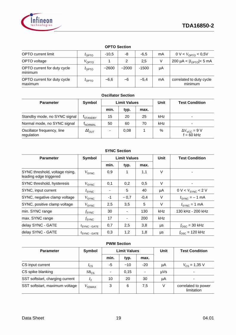
Data Sheet 19 04.01
OPTO current limit IOPTO -10,5 -8 -6,5 mA 0 V < VOPTO < 0,5V
OPTO voltage VOPTO 1 2 2,5 V 200 µA < |IOPTO|< 5 mA
OPTO current for duty cycle minimum
IOPTO −2600 −2000 -1500 µA
OPTO current for duty cycle maximum
IOPTO −6,6 −6 −5,4 mA correlated to duty cycle minimum
Oscillator Section
Parameter Symbol Limit Values Unit Test Condition
min. typ. max.
Standby mode, no SYNC signal fSTANDBY 15 20 25 kHz -
Normal mode, no SYNC signal fNORMAL 50 60 70 kHz -
Oscillator frequency, line regulation
∆fOUT - 0,08 1 % ∆VVCC = 9 Vf = 60 kHz
SYNC Section
Parameter Symbol Limit Values Unit Test Condition
min. typ. max.
SYNC threshold, voltage rising, leading edge triggered
VSYNC 0,9 1 1,1 V -
SYNC threshold, hysteresis VSYNC 0,1 0,2 0,5 V -
SYNC, input current ISYNC - 5 40 µA 0 V < VSYNC < 2 V
SYNC, negative clamp voltage VSYNC -1 −=0,7 -0,4 V ISYNC = – 1 mA
SYNC, positive clamp voltage VSYNC 2,5 3,5 5 V ISYNC = 1 mA
min. SYNC range fSYNC 30 - 130 kHz 130 kHz - 200 kHz
max. SYNC range fSYNC 17 - 200 kHz
delay SYNC - GATE tSYNC - GATE 0,7 2,5 3,8 µs fOSC = 30 kHz
delay SYNC - GATE tSYNC - GATE 0,3 1,2 1,8 µs fOSC = 120 kHz
PWM Section
Parameter Symbol Limit Values Unit Test Condition
min. typ. max.
CS input current ICS -5 −10 -20 µA VCS = 1,35 V
CS spike blanking SBCS - 0,15 - µVs -
SST softstart, charging current I2 10 20 30 µA -
SST softstart, maximum voltage VSSMAX 3 6 7,5 V correlated to power limitation
OPTO Section
TDA16850-2
Data Sheet 20 04.01
SST voltage at power limitation max.
VPLIMAX 5,0 6,0 7,5 V fOSC = 30 kHz
SST voltage at power limitation min.
VPLIMIN 3,0 3,8 4,6 V fOSC = 120 kHz
GATE Section
Parameter Symbol Limit Values Unit Test Condition
min. typ. max.
GATE low voltage VGATE 0,5 0,85 1,2 V VVCC = 2 VIGATE = 5 mA
0,7 1,0 1,5 V VVCC = 2 VIGATE = 20 mA
0,05 0,25 0,35 V IGATE = 50 mA
– 0,5 −0,25 -0,05 V IGATE = – 50 mA
GATE high voltage VGATE 10 11 12 V VVCC = 16 VCL= 4,7 nF
8 9,7 10 V VVCC = 10 VCL= 4,7 nF
7 8 9 V VVCC = 9 VCL= 4,7 nF
GATE rise time tr 120 210 380 ns VGATE = 2 V to 8 VCL = 4,7 nF
30 50 100 ns VGATE = 2 V to 4.5 VCL = 4,7 nF
GATE fall time tf 50 80 130 ns VGATE = 9 V to 2 VCL = 4,7 nF
GATE current, peak, rising edge
IGATE – 1 0,4 - A CL = 4,7 nF
GATE current, peak, falling edge
IGATE - 1,2 2 A CL = 4,7 nF
GATE step voltage VGATE 5 6 7 V -
GATE charge QGATE 150 nC fOSC = 130 kHzpackage P-DIP-8
PWM Section
Parameter Symbol Limit Values Unit Test Condition
min. typ. max.
TDA16850-2
Data Sheet 21 04.01
ERROR Section
Parameter Symbol Limit Values Unit Test Condition
min. typ. max.
CS slew rate minimum (Mains Undervoltage)
SRCS 15 45 70 mV /µs IOPTO = 4 mAfOSC = 30 kHz
VCC threshhold voltage (IC Supply Overvoltage)
VVCCmax 21 23 28 V -
Temperature protection (IC Overtemperature)
TJ 135 145 155 °C -
VREG min. voltage (VREG Loop Failure )
VVREG 2,3 3 3,3 V VSST > 2,6V
VSST max. voltage (VREG Loop Failure )
VSST 2,0 2,6 3,1 V VVREG < 3V
VCC threshhold voltage(IC Supply Undervoltage)
VVCCDWN 7,0 8.0 8,5 V -
VCC protection mode discharging current
I1 10 13 20 mA VVCC = 11V
SST protection mode discharging current
I3 1 2,5 4 mA VSST = 5V
Delay time failure latch active tdelay 30 70 110 µs -
CS threshold voltage(Over current detection)
VCS OC 1,1 1,2 1,3 V -
SST discharge current, at over current detection
IDISC 1,5 3 4,5 mA VSST = 5VVCS = 2V
CS threshold voltage(Short circuit detection)
VCS SC 1,35 1,5 1,65 V -
TDA16850-2
Data Sheet 22 04.01
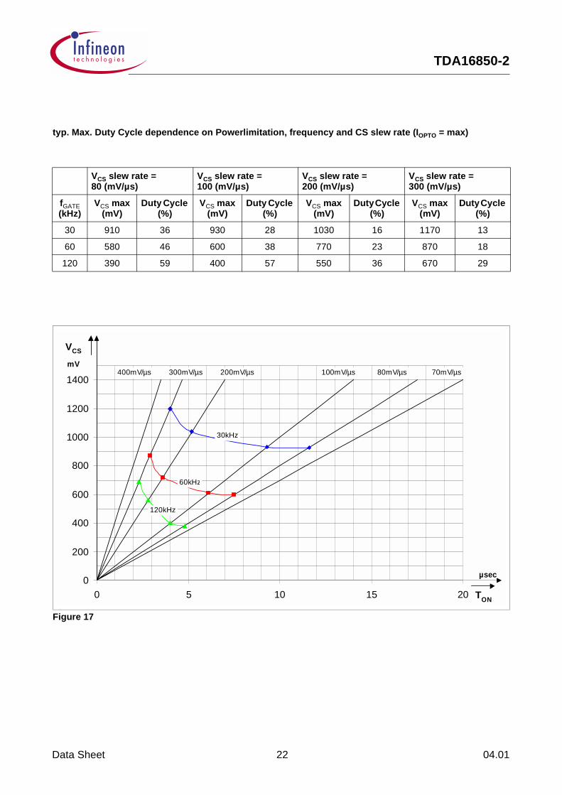
typ. Max. Duty Cycle dependence on Powerlimitation, frequency and CS slew rate (IOPTO = max)
Figure 17
VCS slew rate = 80 (mV/µs)
VCS slew rate = 100 (mV/µs)
VCS slew rate = 200 (mV/µs)
VCS slew rate = 300 (mV/µs)
fGATE (kHz)
VCS max (mV)
Duty Cycle (%)
VCS max (mV)
Duty Cycle (%)
VCS max (mV)
Duty Cycle (%)
VCS max (mV)
Duty Cycle (%)
30 910 36 930 28 1030 16 1170 13
60 580 46 600 38 770 23 870 18
120 390 59 400 57 550 36 670 29
0
200
400
600
800
1000
1200
1400
0 5 10 15 20
300mV/µs400mV/µs 200mV/µs 100mV/µs 80mV/µs 70mV/µs
120kHz
30kHz
60kHz
µsec
VCS
mV
TON
TD
A16850-2
Data S
heet 23
04.01
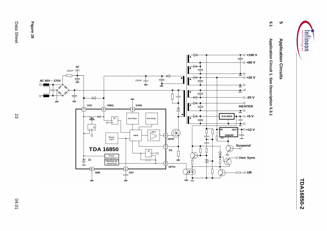
5 A
pp
lication
Circu
its
5.1 A
pp
lication
Circu
it 1. See D
escriptio
n 5.3.1
Fig
ure 18
HEATER
+5 V
-20 V
GND
AC 90V ~ 270V
TLE 4264
OffSST
VCC VREG SYNC
GATE
OPTO
CS
Vert. Sync
IN OUT +12 VON/OFF
Suspend
+80 V
+190 V
+20 V
DRV
PWMPowerlimit
TDA 16850
Z1
5 1
3
6
427
8
Oscillator Overtemp.
Starting-upHysteresis
PowerManagement
220nF
220nF
TD
A16850-2
Data S
heet 24
04.01
5.2 A
pp
lication
Circu
it 2. See D
ecriptio
n 5.3.2
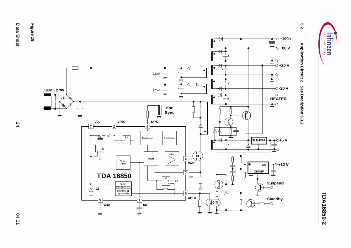
Fig
ure 19
GND
C 90V ~ 270V
Hor.Sync
StandbySST
VCC VREG SYNC
GATE
OPTO
CS
+80 V
+190 V
+20 V
-20 V
HEATER
IN OUT +12 VON/OFF
Suspend
+5 VTLE 4264
DRV
PW MPowerlimit
TDA 16850Z1
5 1
3
6
427
8
Oscillator Overtemp.
Starting-upHysteresis
PowerManagement
220nF
220nF
TDA16850-2
Data Sheet 25 04.01
5.3 Description of Application Circuits
The Application Circuits shows two typical Monitor Power Supplies with a wide input voltage range ( 90 - 230 VAC) and several outputs (+190 V, +80V, +20V, -20V, +12V, Heater, +5V ).
5.3.1 Application Circuit 1
Switch on via connector “Vert. Sync”. Switch off via connector “Off”. From off mode to startup mode via “Vert.Sync”. The Power consumption in off mode is less then 1 Watt. This application needs minimal externalcomponents. This application work with 20kHz in startup and standby mode and 60 kHz in normal mode provided by the internaloscillator.
5.3.2 Application Circuit 2
Switch on and switch off via connector “Standby”. No off mode. The 5 V output therefore is always on. Switchoverof TLE 4264 input to 80 V winding automatically if the winding voltage becomes too low.In normal mode the oscialltor is synchronized via pin SYNC.
Published by Infineon Technologies AGSt.-Martin-Strasse 53D-81541 München
© Infineon Technologies AG 2001All Rights Reserved.
Attention please!
The information herein is given to describe certain components and shall not be considered as warranted characteristics.Terms of delivery and rights to technical change reserved.We hereby disclaim any and all warranties, including but not limited to warranties of non-infringement, regarding circuits, descriptions and charts stated herein.Infineon Technologiesis an approved CECC manufacturer.
Information
For further information on technology, delivery terms and conditions and prices please contact your nearest Infineon Technologies Office in Germany or our Infineon Technologies Representatives worldwide (see address list).
Warnings
Due to technical requirements components may contain dangerous substances. For information on the types in question please contact your nearest Infineon Technologies Office.Infineon Technologies Components may only be used in life-support devices or systems with the express written approval of Infineon Tech-nologies, if a failure of such components can reasonably be expected to cause the failure of that life-support device or system, or to affect the safety or effectiveness of that device or system. Life support devices or systems are intended to be implanted in the human body, or to support and/or maintain and sustain and/or protect human life. If they fail, it is reasonable to assume that the health of the user or other persons may be endangered.
Related Documents