DOE/JPL-1012-7813 Distribution Category UC -63 LSA Project Task Report 5101-56 Structure of Deformed Silicon and Implications for Low Cost Solar Cells (NASA-CR-1561F6) STRUCTURE OF DEFORMED N78-21600 SILICON AND I" P LTCATICIS FCR LCf COST SCLAR CELLS (Jet Propulsion Lab.) 25 p HC A02/MF A01 CSCL 191 Unclas -33/44 14099 Prepared for Department of Energy by Jet Propulsion Laboratory California Institute of Technology Pasadena, California (JPL PUBLICATION 78-13)

Welcome message from author
This document is posted to help you gain knowledge. Please leave a comment to let me know what you think about it! Share it to your friends and learn new things together.
Transcript
I
DOE/JPL-1012-7813Distribution Category UC -63LSA Project
Task Report5101-56
Structure of Deformed Siliconand Implications for Low CostSolar Cells
(NASA-CR-1561F6) STRUCTURE OF DEFORMED N78-21600SILICON AND I" P LTCATICIS FCR LCf COST SCLARCELLS (Jet Propulsion Lab.) 25 p HC A02/MFA01 CSCL 191 Unclas
-33/44 14099
Prepared forDepartment of Energyby
Jet Propulsion LaboratoryCalifornia Institute of TechnologyPasadena, California(JPL PUBLICATION 78-13)
Prepared by the jet Propulsion laboratory, California Institute of Technology,for the Department of Energy by agreement with the National ..cronautics andSpace Administration.
The ) PL Low-Cost Solar Array Project is sponsored by the Department of Energy(DOE) and forms part of the Solar Photovoltaic Conversion Program to initiate amajor effort toward the development of low-cost molar arrays.
This report was prepared as an account of work sponsored by the United StatesGovernment. Neither the United States nor the United States Department ofEnergy, nor any of their employees, nor any of their contractors, subcontractors,or their employees, makes any warranty, express or implied, or assumes any legalliability or responsibility for the accuracy, completenem or usefulness of anyinformation, apparatus, product or process disclosed, or represents that its usewould not infringe privately owned rights.
Il
LSA ProjectTask Report
DOE/JPL-1012-7813Distribution Category UC-63
5101-56
Structure of Deformed Siliconand Implications for Low CostSolar Cells
N. MardesichM. H. LeipoldG. B. TurnerT. G. Digges, Jr.
March 1, 1978
Prepared forDepartment of EnergybyJet Propulsion LaboratoryCalifornia Institute of TechnologyPasadena, California(JPL PUBLICATION 78-13)
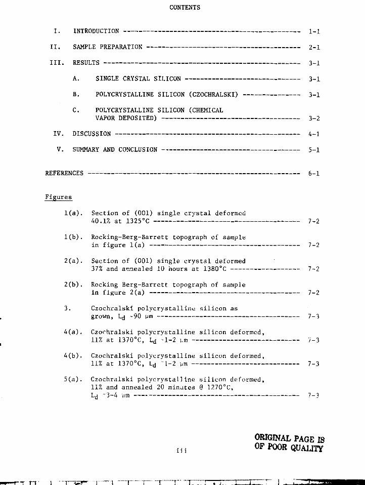
CONTENTS
I. INTRODUCTION ---------------------------------------------- 1-1
II. SAMPLE PREPARATION ---------------------------------------- 2-1
III. RESULTS --------------------------------------------------- 3-1
A. SINGLE CRYSTAL SILICON ------------------------------ 3-1
B. POLYCRYSTALLINE SILICON (CZOCHRALSKI) --------------- 3-1
C. POLYCRYSTALLINE SILICON (CHEMICALVAPOR DEPOSITED) ------------------------------------ 3-2
IV. DISCUSSION ------------------------------------------------ 4-1
V. SUMMARY AND CONCLUSION ------------------------------------ 5-1
REFERENCES------------------------------------------------------- 6-1
Figures
1(a). Section of (001) single crystal deformed40.1% at 1325 0 C ---------------------------------- ---- 7-2
1(b). Rocking-Berg-Barrett topograph of samplein figure 1(a) ----------------------------------- ---- 7-2
2(a). Section of (001) single crystal deformed37% and annealed 10 hours at 1380°C -------------- ---- 7-2
2(b). Rocking Berg-Barrett topograph of samplein figure 2(a) ----------------------------------- ---- 7-2
3. Czochralski polycrystalline silicon asgrown, Ld -90 um ---------------------------------- ---- 7-3
4(a). Czochralski polycrystalline silicon deformed,11% at 1370°C, Ld -1-2 um ------------------------ ---- -3
4(b). Czochralski polycrystalline silicon deformed,11% at 1370°C, Ld `1-2 Um ------------------------ ---- 7-3
5(a). Czochralski polycrystalline silicon deformed,11% and annealed 20 minates @ 1?-70°C,
Ld `3-4 um ---------------------------------------- ---- 7-1
ORIGINAL PAGE ISOF POOR QUALITYii i
5101-56
5(b). Czochralski polycrystalline silicon, deformed111 and annealed 20 minutes @ 1270°C,
Ld~3-4 um ------------------------------------------- 7 -4
6(a). Czochralski polycrystalline silicon, deformed11%, annealed 20 minutes and deformed 11%@ 1370°C, Ld < 1 pm ---------------------------------- 7 -4
6(b). Czochralski polycrystalline silicon, deformed11,7., annealed 20 minutes and redeformed 11%@ 1370 C, Ld <1 um ----------------------------------- 7 -4
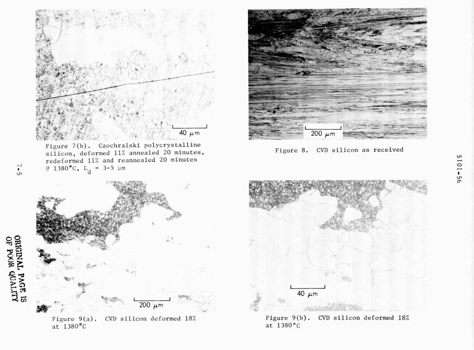
7(a). Czochralski polycrystalline silicon, deformed11%, annealed 20 minutes, redeformed 11% andre-annealed 20 minutes @ 1380°C, I.d = 3-5 m --------- 7-4
7(b). Czochralski polycrystalline silicon, deformed11% annealed 20 minutes, redeformed andre-annealed 20 minutes @ 1380°C, Ld = 3-5 pm --------- 7-5
8. CVD silicon as received ------------------------ ------ 7-5
9(a). CVD silicon deformed 18% at 1380°C -------------- ----- 7-5
9(b) CVD silicon deformed 18% at 1380°C ------------------- 7-5
10. CVD silicon deformed 30% and annealed 10 minutesC 1380 0 C ---------------------------------------------- 7 -6
11(a). CVD silicon deformed 18% annealed 15 minutesand redeformed 30% @ 1380°C -------------------------- 7-6
11(b). CVD silicon deformed 18% annealed 15 minutesand redeformed 30% @ 1380°C -------------------------- 7 -6
12(a). CVD silicon deformed 300 , annealed 10 minutes,redeformed 30% and reannealed 10 minutes@ 1380 0C --------------------------------------------- 7-6
12(b). CVD silicon deformed 30% annealed 10 minutes,redeformed 30% and reannealed 10 minutes@ 1380 0 C --------------------------------------------- 7-7
13(a). CVD silicon deformed 51.6% @ 1340°C ------------------ 7 -7
13(b). CVD silicon deformed 51.6% @ 1340°C ------------------ 7-7
14(a). CVD silicon deformed 18.6% and annealed30 minutes @ 1380°C ---------------------------------- 7-7
IV
5101-56
14(b). CVD silicon deformed 18.6% and annealed30 minutes @ 1380°C ---------------------------------- 7-8
15(a). CVD silicon deformed 421 and annealed10 hours @ 1300% ------------------------------------ 7 -8
15(b). CVD silicon deformed 42% and annealed10 hours @ 1300% ------------------------------------ 7-8
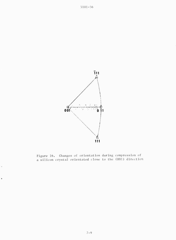
16. Changes of orientation during compression ofa silicon crystal orientated close to the001 direction 7-9
Table
I. Summary of Specimens Investigated -------------------- 7-1
v
5101-56
NOTE
N. Mardesich is presently with Spectrolab, Sylmar, California.
vi
5101-56
ABSTRACT
z
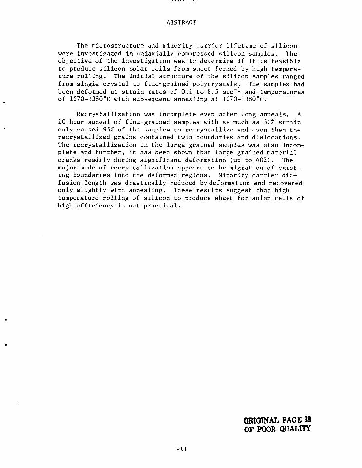
The microstructure and minority carrier lifetime of silicon
were investigated in uniaxially compressed silicon samples. The
__- - objective of the investigation was to determine if it is feasibleto produce silicon solar cells from sheet formed by high tempera-ture rolling. The initial structure of the silicon samples rangedfrom single crystal to fine-grained polycrystals. The samples hadbeen deformed at strain rates of 0.1 to 8.5 sec -1 and temperaturesof 1270-1380°C with subsequent annealing at 1270-1380°C.
Recrystallization was incomplete even after long anneals. A10 hour anneal of fine-grained samples with as much as 51% strainonly caused 95% of the samples to recrystallize and even then therecrystallized grains contained twin boundaries and dislocations.The recrystallization in the large grained samples was also incom-plete and further, it has been shown that large grained materialcracks readily during significant deformation (up to 40%). Themajor mode of recrystallization appears to be migration of exist-
-° iiLg boundaries into the deformed regions. Minority carrier dif-fusion length was drastically reduced by deformation and recoveredonly slightly with annealing. These results suggest that hightemperature rolling of silicon to produce sheet for solar cells of
F=
high efficiency is not practical.
ORIGINAL PAGE I8OF POOR QUALITY
Vii
5101-56
I. INTRODUCTION
Silicon is a material with potential for low cost photovoltaicenergy conversion. One possible method to form silicon sheet materialwhich can then be converted into solar cells is hot rolling. Inves-tigations have demonstrated that high temperature deformation is
possible( 1) . However, there remain questions as to whether the struc-ture of the recrystallized material will permit the fabrication of high
efficiency solar cells.
The most important figure of merit for silicon to be used in solarcells is the effective minority carrier diffusion length (Ld ) (2) which
depends on both grain size and intragrain diffusion length. Investiga-tors( 3-6) have demonstrated that effective diffusion lengths in therange of 30 pm minimum are necessary for high efficiency solar cells(>12%), while shorter effective diffusion lengths are indicative of
lower efficiencies. Several investigators have shown that effectivediffusion length is no larger than the grain size and may be substan-
tially less( 2 , 7 , 8 ). High efficiency cells, then, require grains largerthan 30 um. In addition, structure within the grains may limit theintragrain diffusion length and hence the effective diffusion length.Many large grain ribbon materials, which have intersecting twin planesand dislocations, also have short diffusion lengths( 3 -6 ) and lowefficiencies.
The purpose of this paper is to describe the structure of recrys-tallized silicon and its behavior with respect to deformation rates andannealing cycles. The paper further assesses the implications ofrecrystallized structure on high efficiency solar cells and cost.
1-1
2-1
5101-56
II. SAMPLE PREPARATION
A variety of starting grain sizes and structures was investigated.
Large single crystals as well as 1 mm grain size polycrystals wereobtained from the Czochralski growth process. Fine-grained polycrystals
were obtained from the chemical vapor deposition (CVD) process. Samples,for which minority diffusion lengths were to he measured, were lightlydoped with boron to about 7 ohm-cm resistivity. All samples were
deformed under compression at high temperatures (1270 0 to 1380°C) with
varying deformation rates under a separate study using Instron and MTS
machines (9-11) , During deformation, it was noted that the coarser
grained and single crystal material was more susceptible to crackingunder test conditions. Cracking occurred at approximately 25% strainfor the coarse grained material while cracking occurred at approximately
50% strain for the fine-grained material. A summary of the samplesinvestigated and the deformation conditions is given in Table I. Thistable provides details of the deformation and annealing conditions
Lescribed below.
The samples were prepared for metallography by slicing into 0.5 mm
sections, mounting, and polishing to 0.05 um alumina powder with an
automatic Syntron Polisher. The samples were then Sirtl ctched (12) for
5 to 10 seconds.
V
5101-5b
III. RESULTS
The results of st , adies of these deformed samples are subdividedaccording to the nature of the starting material.
A. SINGLE CRYSTAL SILICON
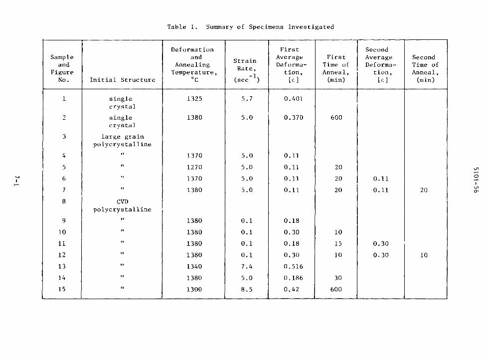
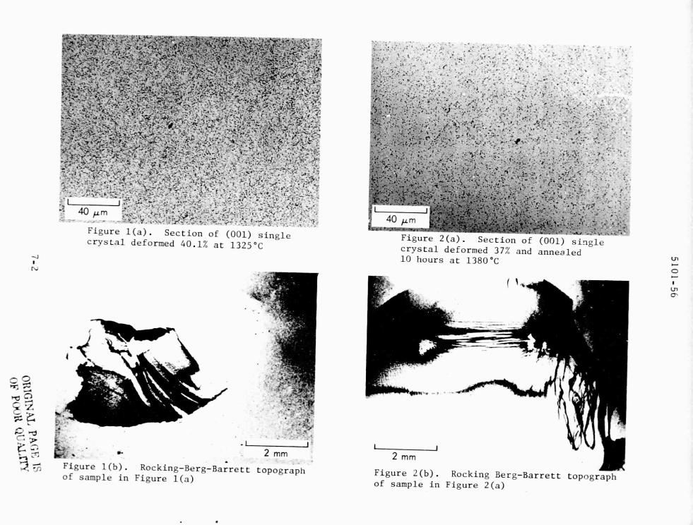
The starting material was Czochralski-grown (001) single crystaland was dislocation free. Figure 1(a) is a photomicrograph of a typicalarea of (001) single crystal after deformation. Dislocations with anaverage density of 10 5cm-2 were generated during the deformation process.Three separate x-ray techniques were utilized to evaluate the resultingstructure and results are summarized below:
(1) Streaking of the Laue spots was observed in back-reflectionx-ray Laue patterns.
(2) Only 15% of the sample was diffracted as a visible image inthe Berg-Barrett test where the sample was rocked 12.5°using a 0.25° divergent beam. The diffracted image isshown in Figure 1(b) and it is noticed that the dislocationdensity was too high to be resolved.
(3) Using a 3° divergent slit, a diffractomer scan gave twopeaks 0.11° apart indicating two crystals.
After annealing for 10 hours, the structure shown in Figure 1(a)changed to that shown in Figure 2(a). The dislocation density in thesephotomicrographs is reduced to 5 x 10 4 cn--2 . The Laue x-ray topographrevealed streaking of the spots; 40% of the Berg Barrett topograph gavea visible image with the dislocation density unresolvable [Figure 2(b)].
However, the diffraction scan on these samples only indicated one peak(one crystal).
The dislocation densities of both samples are approximately the
same but the lattice rotation appears to be smaller in the annealedsamples. The samples experienced some recovery during anneal, but thesmall amount was only evident when complementary results from the variousmethods were obtained.
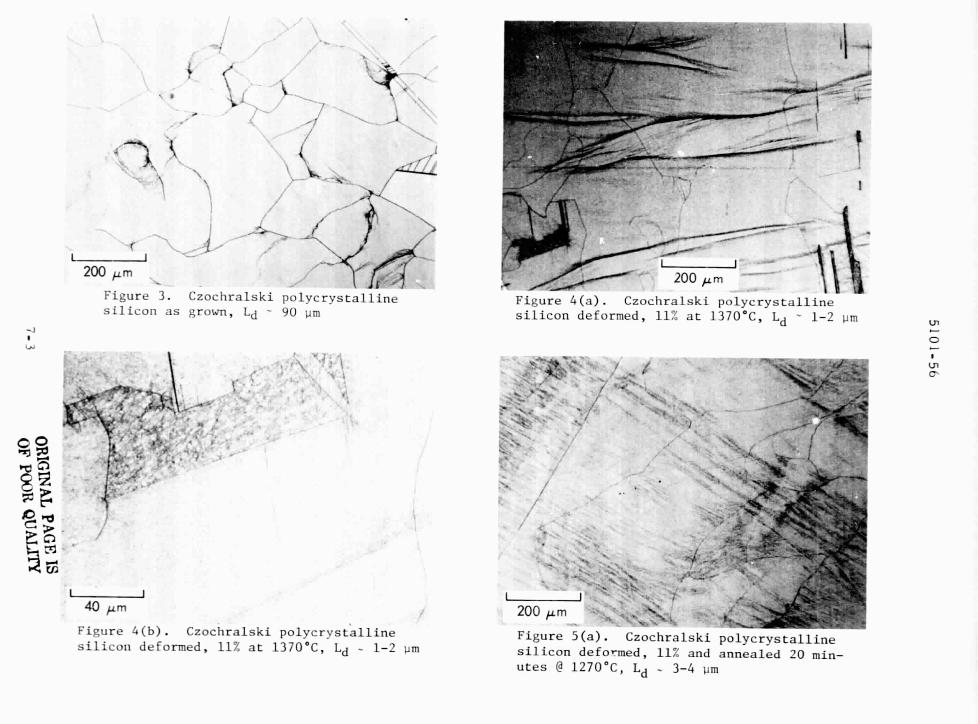
B. POLYCRYSTALLINE SILICON (CZOCHRALSKI)
The structure of Czochralski grown polysilicon prior to deform,-
tion is shown in Figure 3. Minority carrier diffusion length wasmeasured by the surface photovoltage (SYV) method and found to be about90 tim. Figures 4(a) and 4(b) are micrographs shoving the silicon afterthe initial deformation and some dynamic recrystallization. 'These show
ORIGINAL PAGE IS
OF POOH QUAL 14
3-1
f
5101-56
a grain size of about 0.2 mm with a moderately h{.gh, inhomogeneousdistribution of dislocations stretching across the grain boundaries.The grains were present before the deformation had occurred (seeFigure 3) and do not appear affected by the deformation. Diffusion
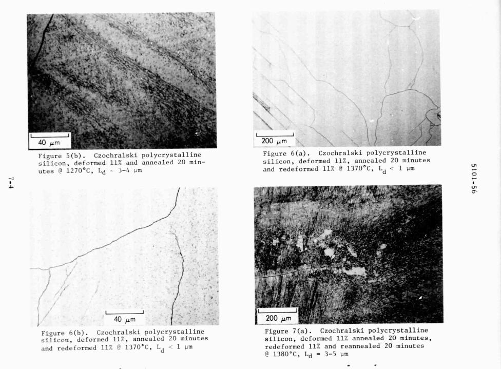
length was reduced to 1-2 um. Figures 5(a) and 5(b) are micrographs ofa similarly deformed specimen after a 20 minute anneal at a slightlylower temperature. The structure is very similar to that of Figures4(a) and 4(b) except that a more pronounced dislocation network appearsto be forming. Diffusion length recovered only slightly to 3-4 pm.Figures 6(a) and 6(b) are micrographs of a redeformed specimen, e.g.,a specimen initially deformed and annealed, then deformed again. The
dislocation networks appear to have polygonized into subgrain boundaries.There is still a high density of dislocations and the grains seem tohave more kinks and discontinuities. Diffusion length degraded to
0-1 um. The last sample of this sequence is a reannealed specimen
[Figures 7(a) and 7(b)]. These specimens show a more pronounced defor-mation structure, resulting in subgrain boundary creation and migrationaccompanied by high dislocation density. They do not seem to show
improvement in structure after annealing comparable to that evidencedby singly deformed and annealed specimens [see Figure 5(b)]. Althoughthe diffusion length did recover to about the same value, none of thesespecimens except the undeformed one would be expected to be structurallygood for solar cells because of the high dislocation densities. Thediffusion length measurements support this expectation. The structureappears to ha v e degraded as more processing was performed.
C. POLYCRYSTALLINE SILICON (CHEMICAL VAPOR DEPOSITED)
The structure of polycrystalline CVD silicon supplied by DowCorning is shown in Figure 8. Figures 9(a) and 9(b) are micrographs of
a random area of a specimen after the initial deformation at<0.1 sec -1 and some dynamic recrystallization. (See Table I for
details.) The micrographs show almost dislocation- ree recrystallized0.5 mm grains in 70% of the material. The dislocations in the remaining30% seem to have coalesced to form small grains of about 2.0 um.
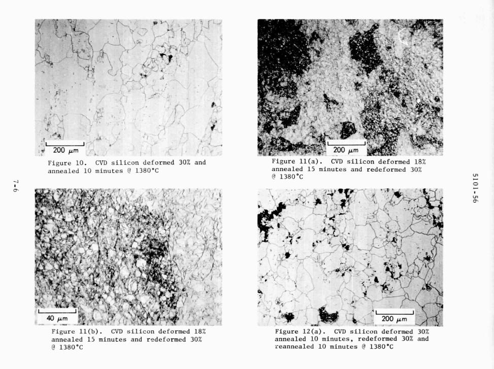
Figure 10 is a micrograph of a specimen after a 10 minute anneal at thesame temperature. The structure is very similar to that of Figure 9(a),
except that 95% of the material has recrystallized. Figures 11(a) and11(b) are micrographs of the redeformed sample showing a I to 2 um grainsize with high dislocation densit y . Remains of the prior grain boun-daries can be seen in Figure il(a), whereas in Figure 11(b) the tworegions seem to be distinguished by the amount of deformation that has
occurred in each of the grains. Apparently, adjacent grains do notexperience equal deformation. Figures 12(a) and 12(b) show how the
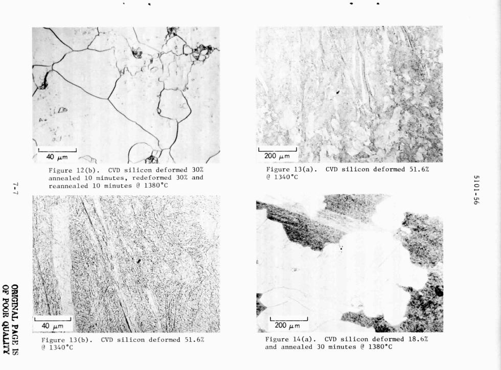
silicon appears after a second deformation and a 10 minute anneal.About 901 of the silicon has recrystallized leaving the grains decoratedwith dislocations. Again, as more processing was performed, the struc-ture became more degraded.
peformation at rates of 5.0 to 8.5 sec -1 was also performed onCVi) silicon at 1380°C. Prior to deformation the CVD silicon was
3-2
5101-56
annealed at 1380% for 24 hours with no apparent change in texture(i)Figures 13(a) and 13(b) show micrographs of two random areas of a
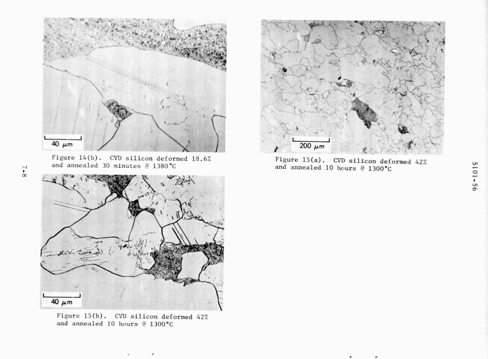
specimen after the initial deformation. The specimen is highly deformedwith very little recovery. After a 30 minute anneal, Figures 14(a) and14(b), 50% of the specimen has recrystallized. The recrystallizedregions have dislocations and twin boundaries, whereas the unrecrystal-lized regions seem to have formed 1 pm subgrains. After a 10 hour
anneal at 1300°C, 95% of the specimen has recrystallized, Figures 15(a)and 15(b). The central regions of some recrystallized grains aredecorated with dislocations and twin boundaries while a few grainsappear to have nucleated dislocation-free grains and grown. Completerecrystallization does, not appear to occur with reasonable (short)annealing time.
3-3
^..^. 1W .
5101-56
IV. DISCUSSION
The deformation of the single crystal silicon is more complexthan might be expected because of the specific compression directionchosen <001>. Single crystal silicon will normally deform by fill)<110> slip during uniaxial compression at high temperature (>1200°C)(13).When a sample is deformed parallel to <011>, the orientation is stablewith respect to the deformation axis while it is not when deformedparallel to the <001>. When the <001> direction is chosen for compres-sion, deformation is accompanied by both lattice rotation and dislocationformation. If the sample is not compressed exactly in the <001> direc-tion, only one slip system is active and the direction of compressionrotates toward the normal to the glide plane [1111 (Figure 16). Therotation overshoots the boundary between the <011> and <100> and asecond slip system becomes active. If the stress is continued, thecompression direction zig-zags across the boundary between the <001> and<011> until it stabilizes its compression axis on the <011> direction.This same type of lattice distortion occurs whether the ends of thespecimen are constrained or not. The change in the direction ofcompression described does not occur simultaneously or uniformly overthe entire crystal, so the sample displays non-uniform deformation andthere is a mismatch of the planes resulting in the creation ofdislocations.
A polycrystalline specimen has an additional constraint to satisfy;the matching of grain boundaries. Deformation of each grain in a poly-crystalline material is dependent on grain orientation with respect tothe compression axis, so the deformation process in polycrystallinesamples is even more non-uniform. Dislocations will form clusters,braids, rings, loops and tangles [Figure 4(a) and 4(b)].
As expected, the observed annealing phenomena varied depending onthe prior deformation and annealing temperatures. At the annealingtemperatures used here, the dislocations in silicon are mobile. Dislo-cations glide and climb in order to annihilate each other or form lowerenergy configurations. The recrystallization of deformed silicon occursby either nucleation and growth of new dislocation-free grains or by
_ strain-induced boundary migration, i.e., migration of existing grainboundaries or of subgrain boundaries which are formed by the coalescenceof dislocations. In the case of nucleation, the boundaries of the newgrains will grow into the deformed grains until they impinge on eachother. The resultant nucleated grains are generally free of strain anddislocations. The strain-induced boundary migration of existing grainor subgrain boundaries competes with nucleation and growth. Existinggrain boundaries are either high or low angle; the subgrain boundariesare always low angle. Migrating high angle boundaries consume more ofthe dislocations and twins than the low angle boundaries. The centralregion of an existing grain is decorated by dislocations and twins ifa grain boundary does not migrate through it [Figures 15(a) and 15(b)].
ORIGINAL PAGE I$OF POOR QUALITY
4-1
5101-56
In the case of <000 single crystals, nucleation and growth does notoccur until the sample has been compressed at least 100%( 15 ) becausesubgrain boundary creation by polygonization and migration of grain
boundaries occurs prior to nucleation. Recovery, in the form of dis-location annihilation and other low energy configurations, does takeplace during the anneal. For fine grained material (M) , the stored
energy associated with grain boundaries can be utilized in conjunctionwith deformation energy to aid recrystallization upon annealing.
4-2
5101-56
V. SUMMARY AND CONCLUSION
From the analysis of the microstructure of deformed and annealedsilicon, there is serious doubt that the structures of hot rolledsilicon are consistent with high efficiency solar cells. The kineticsof silicon recrystallization are low at temperatures near the meltingpoint (1380°C). The structure of the material appears to degrade asmore processing is performed, and long anneals (10 hours) do not com-pletely recrystallize the silicon. The resulting recrystallized ;rains
• are decorated with dislocations and twin boundaries. Recrystallizationat practical rates of samples deformed 50% is only possible if theinitial material has an abundance of stored internal energy, such aswith CVD silicon, which can be utilized during recrystallization. Ifthe material has a grain size of approximately 0.1 mm or greater, thestored internal energy in the material is too low for meaningfulrecrystallization. With such grain sizes, the amount of deformation(>>1000 necessary for practical annealing times has been shown tofracture the material during the deformation process( 10 ). Thus the hotrolling of silicon would require impractically large final reductionsin thickness to achieve 0.1 mm grains and low dislocation density afterfinal anneal. It must be noted that although only one sample of eachdeformation and anneal step was performed and the accuracy of any indi-vidual determination is low, the conclusions drawn from the sequence ofsteps are valid.
The investigation of the structure and diffusion length of uni-axial compressed silicon samples strongly suggests that fabrication ofhigh efficiency solar cells by high temperature rolling of silicon isunfeasible because of requirements for excessively large deformationsand long anneals to promote the otherwise sluggish recrystallization.
This paper presents results sponsored under the Low Cost SiliconArray Project at the Jet Propulsion Laboratory, California Institute ofTechnology, under Contract NAS 7-100, sponsored under an inter-agencyagreement between Department of Energy and the National Aeronautics andSpace Administration.
5-1

5101-56
REFERENCES
1. Graham, C. D., Kulkarni, S., Noel, G. T., Pope, D. P., Pratt, B.,and Wolf, M. 1st Quarterly Report, ERDA/JPI. 954506-76/1, "HotForming of Silicon," June 26, 1976.
2. Socolof, S. I. and Isles, P. A., Proc 11th IEEE PhotovoltaicSpecialists Conference 1975, p. 56.
• 3. Schwuttke, G. H., Yang, K. H., and Hezel, R., Technical ProgressReport No. 5, ERDA/JPL 954144-76/3 "Silicon Ribbon Growth by aCapillary Action Shaping Technique," September 15, 1976.
4. Gurtler, R. W., Baghdadi, A., Wise, J., and Ellis, R. J., TechnicalQuarterly Report No. 5, ERDA/JPL 954376-77/2, "Laser Zone Growth ina Ribbon-to-Robbon (RTR) Process," June 1977.
5. Wald, F. V., Third Quarterly Report, ERDA/JPL 954355-77/3, "LargeArea Silicon Sheet by EFG," September 15, 1977.
6. Zook, J. D., et al., Fifth Quarterly Report, ERDA/JPL 954356-77/1,Dip Coating Process, March 31, 1977.
7. Hovel, H. J., Semiconductors and Semimetals, Volume 11, "SolarCells," pp. 103-108, Academic Press, New York, N.Y. (1975).
8. Card, H. C. and Yang, E. S., IEEE Transactions on Election Devices,24, (1977) 397.
9. Graham, C. D., Jr., Kulkarni, S., Noel, G. T., Pope, D. P.,Pratt, B., and Wolf, M., Quarterly Report No. 2, ERDA/JPL954506-76/2, No. 2, "Hot Forming of Silicon Sheet," September 28,1976.
10. Graham, C. D., Jr., Kulkarni, S., Noel, G. T., Pope, D. P., andWolf, M., Quarterly Report No. 3, ERDA/JPL 954506-77/1, "HotForming of Silicon Sheet," January 11, 1977.
11. Graham, C. D., Jr., Kulkarni, S., Noel, G. T., Pope, D. P., andWolf, M., Quarterly Report No. 4, ERDA/JPL 954506-77/2, "HotForming of Silicon Sheet," April 21, 1977.
12. Sirtl, A. E., and Alder, A., Z. Metallk 52, (1961) 529.
13. Kelly, A. and Groves, G. W., Crystallography and Crystal Defects,p. 175, Addison Wesley, Reading, Mass., 1970.
14. Alexander, H. A. and Haasen, P., Solid State Physics, Volume 22,p. 28 ff.
15. Larson, D. C. and Kocks, U. F., Recovery and Recrystallizationof Metals, Himmel, L., (Editor) p. 239, AIME and IntersciencePublishers, Inc., New York, 1963.
ORIGINAL
OOR QU G
6-1OF
ALITY'
5101-5b
7-1
•b o
r+
..G
ro G
o
v
v •r+0
0u
S G
EN
•-^
Cr
E--4 Q
N
ctlb
00G
OO
Gro
^4 O
rM
MO
$4 O
-4 u
Uv
OO
OO
w+
^ O r-1
rro
GO
OO
OO
u1O
OO
Ya
tiv
•ri
ON
NN
HH
!-iM
O
ra E
G
E^O
(x—4
GF d
v ro
Lb
z E
MN
rACb
S,0
WM
H.--I
Hr
-1H
Mri
MV1
H.7
•rlv w
-wO
OO
OO
OO
OO
OO
OO
fT.7 N
6 q
G rl
•riC1
1r,
OO
OO
OH
—1
ri
r•i7
OCn
ro .61
U^+
ro v
^,n
vi
^ncn
^no
00
or`
L4o0
L iY
rfp
Gv
CW
"Cl •rl 4
LnO
OO
OO
OO
OO
OO
Ocd
C H ro U
N00
r,
r\
c0
00w
00w
--T00
OE
( ICt
^ 0
MM
MN
MM
MM
MM
MM
M1•a
v N
r)H
HH
r--i.--1
r-ir--I
Hr-I
Hr-I
r-Iw
C E
dq
F
vCC
t".i..+
C •r1
•ri(J
•rl
r-I
r--IO
r-IH
ro H
Hs,
vro
vro
s^ro
czu
Ha^
H t-j
00 u
qtJ
00m
OA
wN
=_
>CA
roN
UT
Ui+
UU
r1ro
7,
>,
L.--1
1-1
r-i
rlO
O
v
4i
0. 0 7 0
ra
NM
to
110riN
M?
to
E r
o w
zr i
r+r-1
'-+H
Hro
•r+^
w
•
.bvrobD
•ri
LNv9CHNCvEUNaLWOL.ro7Hv
HroF
i. :,fir.%
1"'^^; ^^;;„^
• «^
•',' r^9•^•• .k _314..•n^`^?^••
mot_
^ 1
. • .^(r)^
t
+r•'ti .`'
iir.
,• i..\',•• '^•'
mil.
^-w_^;
N.wa
r--IC"^ vr-•i
r-I ^
^ o
Cv O
W a
O Gro
GO•.a r`
J M U
u4J '^
OV 00
^ M
• O
i , W L
ro v ri
..
•tlN
(A.4c
^>
+O
f1.
1r00
C(S.OJLCWJ
JvN1-i
COI00
^ ro
60 N
C•^ v
u 7
O aw
• G
av
V '-1G
.
lv. ro
to-4 W
.. o
5101-56
^•..: •) it
^Y
+'Y
' 3•P
^̂"`̂
^^ •'If li lL t •.t
~ J̀^
^,5,
!;"^
^^
`;•± 'mss+,
^
{ ^.,^
•'` i ;i.'''^; ^
`}.itsO
R•^
.L
CIO
le
'LY''IIYY
7-2
OF
p oohi•^1
'^i ro
E 00
N °•OJa+vS.a
W100
G q
(qI ^
00 .-1
u 7
^O 44
• C
i
•a,O^ v
.^w^
7
^ ^
^ ^
^^jj ^
^.. L
a• O
^^^ ^ Y
r } ^j•r
q
N N
,
lg
LI
L
U U
/
U ro
-4 C
)O
C
Q
4.1^
44 C
o(n-4
--ro
a:
F"r'•-I
i1
N •b
/' f'
O^~
n W
\^.
v O
1rU
w ^,
,f.;^ 1
^.
n
ro
ro \ M
L+
r-1
f_^j^
O o
6
•
^ W
Oro w
r,•
^ b N
Ev
O
°V^4 u
Q^^ v
(V
L-
N O
iv c
G •-a
• ^4 EO
ro N
l
a^Gr-1roLNu E
OO
G O
^
^ b
rouuO O
N 1
-r
U GCWro
M
Cw
O
Ei°4CV
J
,y
i..N
+1^
5101-56
—EN
^r•-1.
ro
w''^
U7.-7
>^
u U
O r-
n. M
at u
-cn
ro
w ^
R
-N
•
•+^
U
)N
}\
.O
Gl
-"I
7-3
`f'^•r^
J i
b^•Fl^
1t ^
^ ^
.E
v o
` . :t ► .= .,.,
4. to
OR
I(,AN
AL
PA
GE
ISO
F P
OW
It Qt1A
LI'I'Y
i
W
a)
.•17
r--I
C
G
ro E
cn O
T fV
>4U 'D
OT
Ql .-a
rl
.-1o m
a v u
C o
•rlG O
(/JC•1
c0
w -4
"
.0 —4
/UO
i7
NE1•+
b
O
QJ
• w E
in Q
ll+
b o
..w
^O
NG b
!E
N O
w
W U
W:•1-4
' OC
N
^
Gw
m r
o
c v N
-4 i..J
Q)
••^ C
O
ate. E
•^
cnE
T O
f-+ fV
OU
fV
T Q! b
o -A
v
•.-1 G
C1
sL C C
UJ c' C
c7 ^\ CJ E
S-• .-J
1w
^
U b Ln
O b G
I
N Q
J R
1 C
l)
U EL
+ \ II
O .-I
m•0
M
1—
E J
G
1•+ oQ
J O
C O
H U w 00
Q, rn
^o—4
.,..I .,..IQJ
5101-56
i
QW.
y,
or' -y.'A
- -
V
y
7•,r•
I sM
^^
c,
^
• s'
V)v
aJ
—+
C E
c'J
E
IQJ C
G •r+
•4 E
--aO
00.1
f•vvEOwvGOuU
E10p U
T OC
)Q.) 001d M
^ rl
00
•.1 N
P. h
Ni
rl `yII
I1'
^!11.
1,,^
1s
'I^
uv
^,u
.
,1•
•I^'I
1 ^
^11 t^
^^rI
^ 111, ,
I,^'^
v+
^
1li
SIB
1r'
,^^
!w
1
1'{
.-N
rAi,
Ev
iG y m
•r.,-W
y
-^
J^E
m
E
1-I N
Ou
N
O r
1
cuC
L 0
-4v
ca
^^ -
v7c0
G•
.1cy
~ ^
<C
^ v
E
u
•b
Ln
O b
G I
ro
M
hU
^
'L
+ ^
II
jk
O.1
w .-1
v
ebbl
v
y
r'
-v o
0 0G
o
^^
•tc
4
•4
cn
+:s
t
}v
00
•-1 iJ
00•nvEt•.
Ew
iv
CD
GN
Our•-1N
rC]
7•
V
AA
m.^ U
5101-56
- 5
OR
IGIN
AL
pAC
;F', 1S
OF
")H
QL
A"F
"
T
"tj cu
C: w
,I'
ulo
C:—4
• E
•-4 "1= U(V
0
Q) -4 0
0 00
(V en
r. r- 4
-4
r-co S)
ztco0
7-6
0CU 44CU
A^
"o
p
C:0u
4}
—4
o,
L•
:j
1-1
m 00
5101-56
00
. 44w'..4
—4Ilk
w E
0 w
4101
tj
0 coQ)
14
0 00
>
rift
= --4
C:
tip
4
a) ca
Q)
4 w
cz r_ m
C: Q)
L-7
C)0 u
u (2)..4
—4 W
)L-4
Q)
SI
=1Q)
CN
-,4
-jLL.
TF.
III
1,
5101-56
4
10
Ilk1 1
14
41 .A
'n0UUcna 1
J,4
CN
r
f^
jjaa^
^^^ ^
_ —^D,
C> r.
r)
cC
a Q)r= 0
0 00
0"
Q) C2)
W •
Q)(o Aj
_4
C E
•
4E C
_2 1 4
4
A:E
Q)
IN,
7-7
Nr
00-4
U0Cl 00,a0 (niu4 V)
-4 C)
4(n :jr
gm —
> rC)
t
C)
UAW,
LnUufn
^4
4
ORIGINAL PAGE PS
OF POOR QUALITY
i
5101-
}N
J^•
O0
^,,^j, fti
^
J
b OO
ar
" }^
^+ V
1Q
o , ; -'
__
t!
oN4
vC
$4ty
O M •9
•^ C
I
?^
r^
,1
*{
O e
!^
q
T^'^
.
C1 0
0th
J
r. r.-.
t
ps,
-b
i
-El
yr
,e
t
s ^
^, v
04
^• r^ L
i
Nlzr
VGl4.0 U
y e
b O
C ^
O .-1
U•d
C^J
•-4•,4
yU L+
• N I I
UOvG
7! C
E^ w
^
i-8
^^ - _
r ^^- fi
r^+
•.
...,-
-
_
^
5101-56
0
0111
i
001, 0 ^,
it 11,
Figure 16. Changes of orientation during compression of
a silicon crystal orientated close to the (001) direction
7-9
Related Documents