Solution EC Sample Paper 2011 GATECounsellor | E-mail id: [email protected] 0 1. (a) Concept: Determinant = Product of eigen values Trace = Sum of eigen values Solution: Options (b) and (d) satisfy product property only, (c) satisfies sum property only, but only (a) satisfies both. Reference: Higher Engineering Mathematics by B S Grewal, Properties of eigenvalues. 2. (c) Concept: 1. If λ1, λ2, λ3…..λn are eigen values of A then λ1 m , λ2 m , λ3 m …..λn m are eigen values of A m . 2. If λ is eigen value of A then the eigen value of A m +kI is λ m +k. 3. Determinant = Product of eigen values. Solution: The eigen values of are Reference: Higher Engineering Mathematics by B S Grewal, properties of eigenvalues, page 73 3. (c) Concept and Solution: The charging time constant RsC must be short compared with the carrier period 1/fc that is RsC << 1/fc, so that the capacitor C charges rapidly and thereby follows the applied voltage up to the positive peak when the diode is conducting. On the other hand, the discharging time constant RlC must be long enough to ensure that the capacitor discharges slowly through the load resistor Rl between positive peaks of the carrier wave, but not so long that the capacitor voltage will not discharge at the maximum rate of change of the modulating wave, that is 1/fc<<RlC<<1/W, where W is the message bandwidth. For another explanations refer: http://www.st-andrews.ac.uk/~www_pa/Scots_Guide/RadCom/part9/page2.html

Welcome message from author
This document is posted to help you gain knowledge. Please leave a comment to let me know what you think about it! Share it to your friends and learn new things together.
Transcript

Solution EC Sample Paper 2011
GATECounsellor | E-mail id: [email protected]
0
1. (a) Concept:
Determinant = Product of eigen values
Trace = Sum of eigen values
Solution:
Options (b) and (d) satisfy product property only, (c) satisfies sum property only, but
only (a) satisfies both.
Reference: Higher Engineering Mathematics by B S Grewal, Properties of eigenvalues.
2. (c) Concept:
1. If λ1, λ2, λ3…..λn are eigen values of A then λ1m, λ2m, λ3m…..λnm are eigen values of Am.
2. If λ is eigen value of A then the eigen value of Am+kI is λm+k.
3. Determinant = Product of eigen values.
Solution:
The eigen values of are
Reference:
Higher Engineering Mathematics by B S Grewal, properties of eigenvalues, page 73
3. (c) Concept and Solution:
The charging time constant RsC must be short compared with the carrier period 1/fc
that is RsC << 1/fc, so that the capacitor C charges rapidly and thereby follows the applied
voltage up to the positive peak when the diode is conducting. On the other hand, the
discharging time constant RlC must be long enough to ensure that the capacitor discharges
slowly through the load resistor Rl between positive peaks of the carrier wave, but not so long
that the capacitor voltage will not discharge at the maximum rate of change of the modulating
wave, that is 1/fc<<RlC<<1/W, where W is the message bandwidth.
For another explanations refer:
http://www.st-andrews.ac.uk/~www_pa/Scots_Guide/RadCom/part9/page2.html
Solution EC Sample Paper 2011
GATECounsellor | E-mail id: [email protected]
1
4. (c) Concept:
Image Rejection Ratio= , Where
Solution:
=1.386
Thus, Image Rejection Ratio= = 138.64
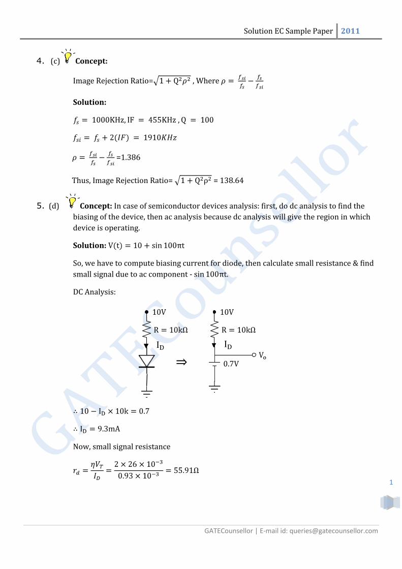
5. (d) Concept: In case of semiconductor devices analysis: first, do dc analysis to find the
biasing of the device, then ac analysis because dc analysis will give the region in which
device is operating.
Solution:
So, we have to compute biasing current for diode, then calculate small resistance & find
small signal due to ac component - .
DC Analysis:
Now, small signal resistance
Solution EC Sample Paper 2011
GATECounsellor | E-mail id: [email protected]
2
AC Analysis:
Reference: Electronic devices and circuit theory by Boylestead
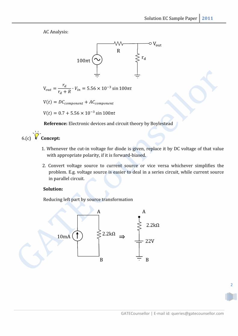
6.(c) Concept:
1. Whenever the cut-in voltage for diode is given, replace it by DC voltage of that value
with appropriate polarity, if it is forward-biased.
2. Convert voltage source to current source or vice versa whichever simplifies the
problem. E.g. voltage source is easier to deal in a series circuit, while current source
in parallel circuit.
Solution:
Reducing left part by source transformation
⇒
Solution EC Sample Paper 2011
GATECounsellor | E-mail id: [email protected]
3
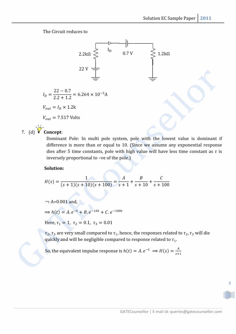
The Circuit reduces to
7. (d) Concept:
Dominant Pole: In multi pole system, pole with the lowest value is dominant if
difference is more than or equal to 10. (Since we assume any exponential response
dies after 5 time constants, pole with high value will have less time constant as is
inversely proportional to –ve of the pole.)
Solution:
A=0.001 and,
Here,
, are very small compared to hence, the responses related to will die
quickly and will be negligible compared to response related to
So, the equivalent impulse response is
Solution EC Sample Paper 2011
GATECounsellor | E-mail id: [email protected]
4
Shortcut: Write H(s) in standard form and remove the pole having difference 10 with the
lowest pole.
Reference: Control systems Engineering. By Nagrath, Gopal
8. (c) Concept:
If
=
Solution: Here, r(t)= 5cos(6t+ ) ;
because, tan is increasing and
9. (a and b)
Concept: Reflection coefficient, and VSWR=
Solution:
(a) Short Load, Reflection Coefficient since ZL=0 and, VSWR=
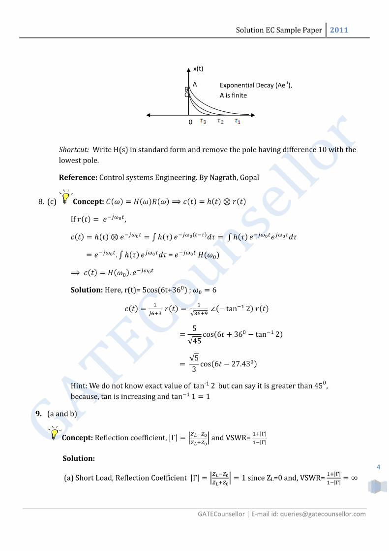
A
B
C
0
Exponential Decay (Ae-t),
A is finite
x(t)
Solution EC Sample Paper 2011
GATECounsellor | E-mail id: [email protected]
5
(b) Open Load, Reflection Coefficient and,
VSWR=
(c) For matched Load, Reflection Coefficient and,
VSWR=
Reference: Elements of Electromagnetics by Sadiku.
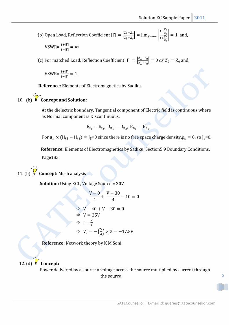
10. (b) Concept and Solution:
At the dielectric boundary, Tangential component of Electric field is continuous where
as Normal component is Discontinuous.
For =0 since there is no free space charge density, , so =0.
Reference: Elements of Electromagnetics by Sadiku, Section5.9 Boundary Conditions,
Page183
11. (b) Concept: Mesh analysis
Solution: Using KCL, Voltage Source = 30V
Reference: Network theory by K M Soni
12. (d) Concept:
Power delivered by a source = voltage across the source multiplied by current through
the source

Solution EC Sample Paper 2011
GATECounsellor | E-mail id: [email protected]
6
Solution: On simplifying the circuit:
Power delivered by the source
13. (b) Concept:
Number of IC’s Required = Total Memory Size/ Size of One Memory IC
Sometimes, calculation needs to be done carefully, given example will give you the fare
idea of concept.
Solution:
In the interfacing we have to use pair of 4K Nibble IC’s to get 4K Byte. So for 24K Byte
we require 12 (4K Nibble) IC’s. Now we are left with 2K Byte memory. Since, we can’t get
2K Byte from a single 4K Nibble IC, we should two IC’s. So total IC’s required= 14 IC’s.
14. (c) Concept: Which instructions affect which flags in microprocessor.
Solution:
1. SP2400H 2. C01H 3. PUSH B means SP decreases to 23FEH,
23FFH(Address)XXH and 23FEH(Address)01H 4. POP PSW means AXXH, Flag register01H=(00000001)2 5. RET. So CY=1 i.e. set and Z=0 i.e. reset Reference: 8085 Microprocessor by Gaonkar
1Ω
1Ω 1Ω
1Ω
1Ω 1Ω
6 V
½ Ω
½ Ω 1Ω
1Ω
6 V
i
Solution EC Sample Paper 2011
GATECounsellor | E-mail id: [email protected]
7
15. (b) Concept:
If f is any function of a surface then (grad f) will the normal to the surface. If we take the dot
product of grad f and the given directional unit vector (if not unit vector we have to convert)
we’ll get the Directional derivative in the direction of the given vector.
Solution:
at P
Directional derivative in the direction of is:
Reference: Elements of electromagnetics by Sadiku
16. (a) Concept: Instability of mainly depend on three factors:
1. Reverse Saturation Current, , which doubles for every 10oC increase in temperature.
2. Base emitter Voltage , which decreases at the rate of 2.5 mV/oC for both Ge and Si
Transistors.
3. which increases with temperature.
Total change in collector current can be calculated by summing the individual changes due to
above three factors.
Here, we are looking variation of with respect to only, as we assume and
sensitivity (Stabilization Factor) of Emitter Bias Configuration circuit with respect to is
defined as,
Higher value of corresponds to higher Instability or sensitivity.
Solution: In Circuit A,
And, In Circuit B,
So, Circuit A is more sensitive to temperature variation.
Solution EC Sample Paper 2011
GATECounsellor | E-mail id: [email protected]
8
THINK!!: Why Sensitivity depends only on these three factors?
Reference:
Integrated Electronics, Millman Halkias, Chapter 9, Section 9-4, Page Number 290.
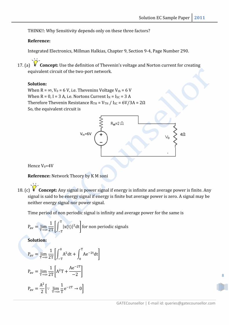
17. (a) Concept: Use the definition of Thevenin’s voltage and Norton current for creating
equivalent circuit of the two-port network.
Solution:
When R = ∞, V0 = 6 V, i.e. Thevenins Voltage Vth = 6 V
When R = 0, I = 3 A, i.e. Nortons Current IN = ISC = 3 A
Therefore Thevenin Resistance RTH = VTH / ISC = 6V/3A = 2Ω
So, the equivalent circuit is
Hence V0=4V
Reference: Network Theory by K M soni
18. (c) Concept: Any signal is power signal if energy is infinite and average power is finite. Any
signal is said to be energy signal if energy is finite but average power is zero. A signal may be
neither energy signal nor power signal.
Time period of non periodic signal is infinity and average power for the same is
Solution:
Vth=6V 4Ω
Solution EC Sample Paper 2011
GATECounsellor | E-mail id: [email protected]
9
So,
Reference: Shaum series on analog and digital communication, Energy Content of a signal and
Parseval’s theorem, Section 1.3.
19. (d) Concept:
=
Proof:
Solution: Given,
20. (d) Concept and Solution:
1.
2.
3.
4. and N=LCM(
Solution EC Sample Paper 2011
GATECounsellor | E-mail id: [email protected]
10
21. (d) Concept: Put and use Boolean rules to simplify.
Solution: If the expression becomes,
Reference: Digital electronics by Morris Mano
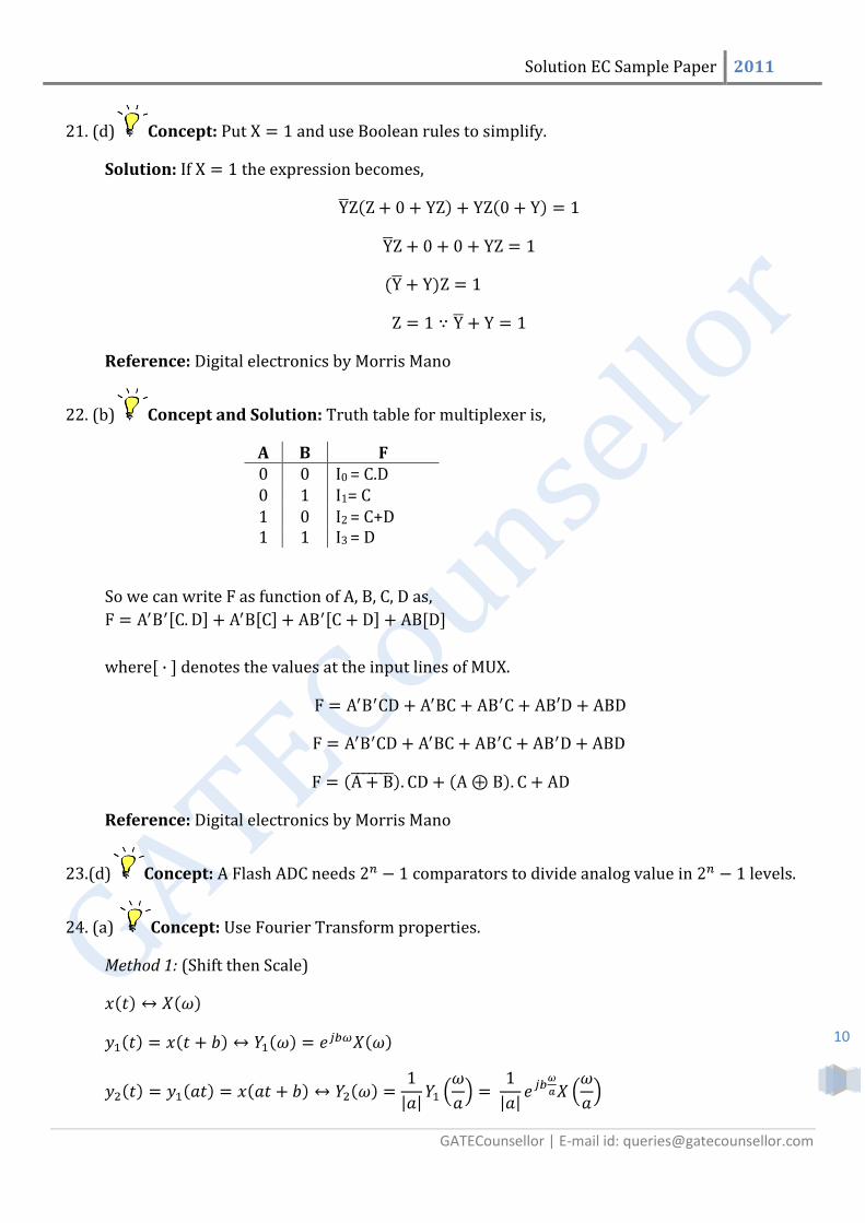
22. (b) Concept and Solution: Truth table for multiplexer is,
A B F 0 0 I0 = C.D 0 1 I1= C 1 0 I2 = C+D 1 1 I3 = D
So we can write as function of A, B, C, D as,
where denotes the values at the input lines of MUX.
Reference: Digital electronics by Morris Mano
23.(d) Concept: A Flash ADC needs comparators to divide analog value in levels.
24. (a) Concept: Use Fourier Transform properties.
Method 1: (Shift then Scale)
Solution EC Sample Paper 2011
GATECounsellor | E-mail id: [email protected]
11
Method 2: (Scale then Shift)
Reference: Signals and Systems by Oppenheim
25. (d) Concept: Methods to calculate residues from poles,
Solutions:
Similarly
Sum of residues
Reference: Higher engineering Mathematics by B S Grewal, Calculation of residues,
section 20.19,
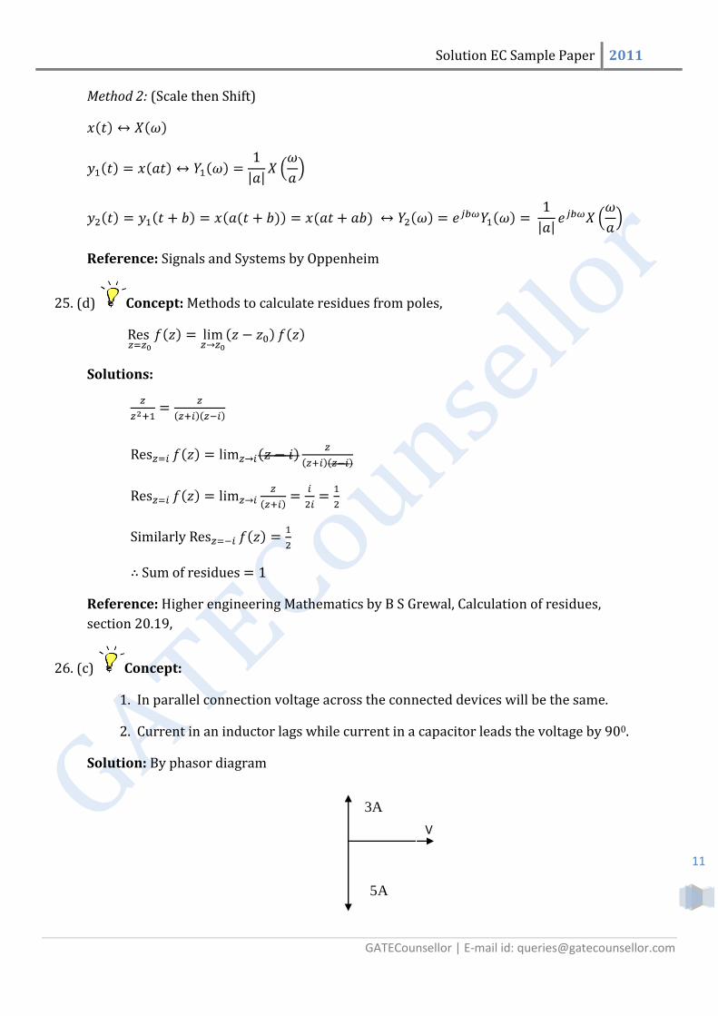
26. (c) Concept:
1. In parallel connection voltage across the connected devices will be the same.
2. Current in an inductor lags while current in a capacitor leads the voltage by 900.
Solution: By phasor diagram
A5
A3
V
Solution EC Sample Paper 2011
GATECounsellor | E-mail id: [email protected]
12
Reading of ammeter A is A235
27. (c) Concept: Definition of time constant form, type and degree for a system:
Time constant form is like,
Then,
n= Type Number of the system = Number of Poles at the origin
Order = Total number of poles = Degree of the denominator polynomial
k= System gain = and
Solution:
H(s) can be written in time constant form as:
So, k
Type = 2 and order = 7
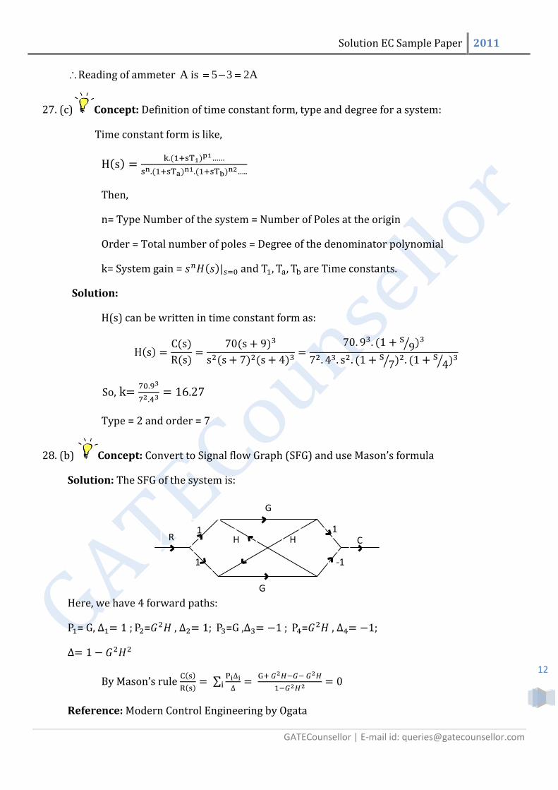
28. (b) Concept: Convert to Signal flow Graph (SFG) and use Mason’s formula
Solution: The SFG of the system is:
Here, we have 4 forward paths:
= G, = , =G , = ,
By Mason’s rule
Reference: Modern Control Engineering by Ogata
G
G
H H 1
1
1
-1
R
RR C
Solution EC Sample Paper 2011
GATECounsellor | E-mail id: [email protected]
13
29.(d) Concept: Find impulse response from transfer function and analyze which waveform
suits it best. E.g. if a sinusoidal term is multiplied, the waveform will have modulation following
the envelope.
(a) ------(A)
(b) -----------(D)
(c) -----------(B)
(d) ------------(C)
Reference: Signals and Systems by Oppenheim or any other (even B S Grewal) for methods to
find inverse Laplace transform
30. (c) Concept and Solution: System A is invertible if system B exists such that when A and B
are cascaded, the output of B is equal to the input of A. B is referred to as the inverse system of
A. Otherwise, A is noninvertible. In an invertible system, For a given output, input can be
determined uniquely also, distinct input leads to distinct output.
So,
31. (c) Concept and Solution: Fourier Transform properties
Reference: Signals and Systems by Oppenheim
32. (c) Concept: Scattering matrix describes the behavior of a linear, multi port device at a given
frequency ω.
Smn= , given that, All of the remaining (unused) ports are loaded
with an impedance identical to the system impedance
A lossless network is one which does not dissipate any power, The sum of the incident
powers at all ports is equal to the sum of the reflected powers at all ports. This implies that the
S-parameter matrix is unitary.
Solution EC Sample Paper 2011
GATECounsellor | E-mail id: [email protected]
14
A reciprocal network is build of passive components, and Scattering matrix parameters are
related as, Smn = Snm
Here, Scattering matrix is,
Here, S12 = S21, it implies Reciprocal Network.
And, it implies a lossy network.
Reference: "Foundations of Microwave Engineering" by R. E. Collin, McGraw Hill or any basic
book of microwave engineering.
33. (b) Concept and Solution: Poynting vector represents the average power flow through the
surface.
Reference: Elements of electromagnetics by Sadiku or Field and Wave electromagnetics by D K
Cheng
34. (b) Concept: At the dielectric boundary Tangential component of Electric field is continuous
where as Normal component is Discontinuous.
This also holds for
And, = 0 , Since there is no free space charge density , so =0.
So,
Since, =>
And, H1= H2
Reference: Elements of electromagnetics by Sadiku (see boundary conditions)
35. (d) Concept: Only INTR is a non-vectored interrupt as the I/O device has to provide the
address of subroutine to be carried out after the interrupt.
36. (b) Concept:
A Moore machine has its output as a function of its present state only. It is independent of
input.
A Mealy machine has its output as a function of its present state as well as inputs supplied.
Reference: Digital computer electronics by Malvino and Brown

Solution EC Sample Paper 2011
GATECounsellor | E-mail id: [email protected]
15
37. (d) Concept and Solution:
Here we get output ‘1’ only when system is in state and input in 1. So the state must go from
. For that to happen we need first input to be 1 so state goes from . Now next we
need to go from for which input ‘0’ is needed. Now we go from state when
input is ‘1’. So whenever sequence ‘101’ occurs we get output ‘1’.
Reference: See state diagram and state table in Digital Design by Morris Mano
38. (c) Concept: 1. Standard diode equation
Where,
Reverse saturation current
Unity for Ge
Temperature equivalent of voltage
Solution: Take Base-Emitter junction,
Here η is taken to be 1, as the diode is sufficiently forward biased.
Reference: Integrated Electronics by Millman and Halkias
39. (b) Concept and Solution:
As reverse bias, at base collector junction is increased, the transition region penetrates deeper
into base collector junction. Penetration of the transition region into base is a much more
pronounced effect as the base is very thin as compared to emitter and collector. The decrease
in the base width has the following effects:
1. There is less chance of hole–electron recombination which increases large signal current
gain α.
2. As junction is more reverse biased, resistance between base and collector increases.
Reference: Integrated Electronics by Millman and Halkias
Solution EC Sample Paper 2011
GATECounsellor | E-mail id: [email protected]
16
40.(c) Concept and Solution: in active region. We know the curve is like
a normal pn junction diode curve shown in (c) or (d). decreases with increase in
temperature. So, with rise in temperature, the exponential curve will shift towards left.
Reference: Integrated Electronics by Millman and Halkias
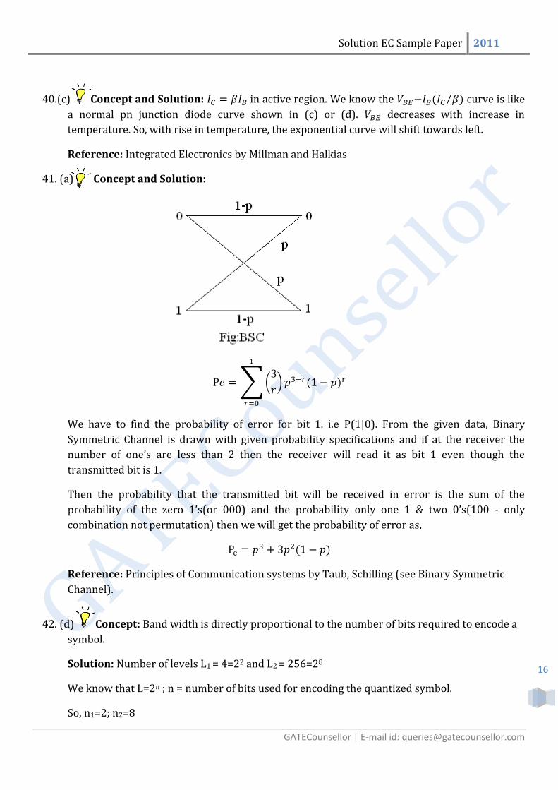
41. (a) Concept and Solution:
We have to find the probability of error for bit 1. i.e P(1|0). From the given data, Binary
Symmetric Channel is drawn with given probability specifications and if at the receiver the
number of one’s are less than 2 then the receiver will read it as bit 1 even though the
transmitted bit is 1.
Then the probability that the transmitted bit will be received in error is the sum of the
probability of the zero 1’s(or 000) and the probability only one 1 & two 0’s(100 - only
combination not permutation) then we will get the probability of error as,
Reference: Principles of Communication systems by Taub, Schilling (see Binary Symmetric
Channel).
42. (d) Concept: Band width is directly proportional to the number of bits required to encode a
symbol.
Solution: Number of levels L1 = 4=22 and L2 = 256=28
We know that L=2n ; n = number of bits used for encoding the quantized symbol.
So, n1=2; n2=8
Solution EC Sample Paper 2011
GATECounsellor | E-mail id: [email protected]
17
As, B.W. n
Factor= n2/n1 = 4
Reference: Principles of Communication systems by Taub, Schilling
43. (b) Concept and Solution: Transconductance(gm) is given by,
Drain current MOSFET in saturation is given by,
: i.e. is linealy varies with .
: i.e varies with square root of the .
Reference: Microelectronics circuits by Sedra and Smith
44. (c) Concept and Solution:
Given, m(t)=
The instantaneous frequency of modulated signal is varied linearly with modulating
signal.
The angle
θi(t) = =
Reference: Communication Systems by Simon Haykin
Solution EC Sample Paper 2011
GATECounsellor | E-mail id: [email protected]
18
45. (a) Concept and Solution: Given, Pt=1mW, BW=100MHz, PL(dB) =-40dB, No=10-20 W/Hz
Si(dB)= Input Power – Power Loss = 10 log Pt – 10 log PL = 10 log (Pt/ PL)
Si = Pt/ PL = 10-3/10-4 = 10-7 W
ni = No* BW = 10-20 x 100 x 106
Si/ ni = 10-7/10-12 = 105 = 50(dB)
Note: Since we are given one-sided psd of noise we take it as No.
46. (b) Concept: See Solution 3, Use
Solution: and W or
47. (c) Concept:
When 0 transmit, the received pulse should be, y0=-A+n
When 1 transmit, the received pulse should be, y1= A+n , where n is AWGN
Probability of eror, Pe = 0.5p(1/0)+p(1/0)
For Proof, Please see Reference.
Solution:
4.27 =
Bit Rate = 1/Tb = 13.71KHz
Reference: B.P.Lathi “Modern digital and analog communication system” 3rd edition,
page no.331
Solution EC Sample Paper 2011
GATECounsellor | E-mail id: [email protected]
19
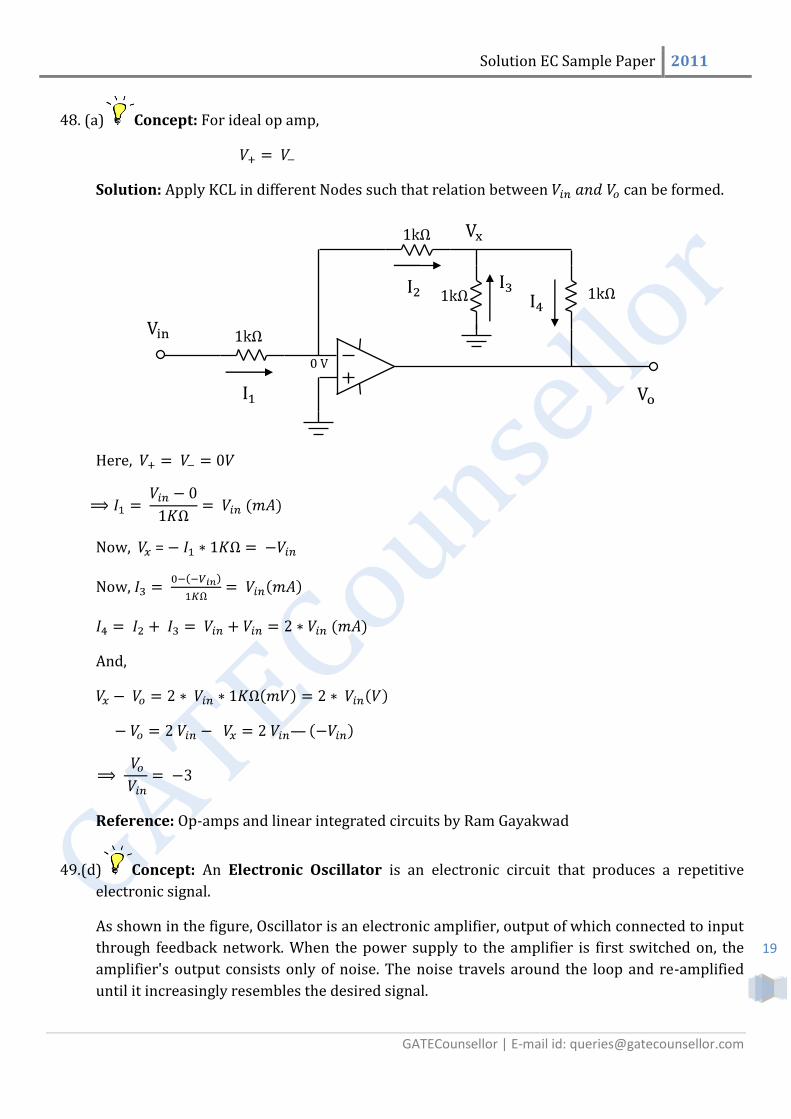
48. (a) Concept: For ideal op amp,
Solution: Apply KCL in different Nodes such that relation between can be formed.
Here,
Now, =
Now,
And,
Reference: Op-amps and linear integrated circuits by Ram Gayakwad
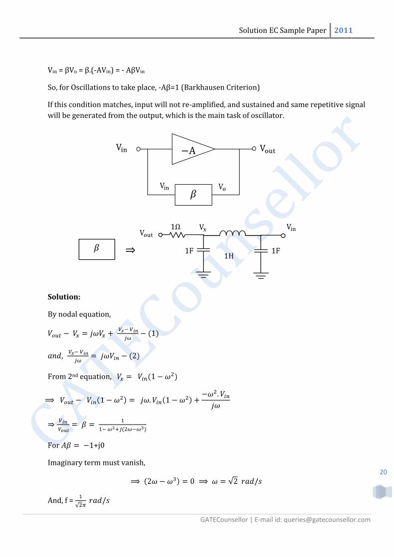
49.(d) Concept: An Electronic Oscillator is an electronic circuit that produces a repetitive
electronic signal.
As shown in the figure, Oscillator is an electronic amplifier, output of which connected to input
through feedback network. When the power supply to the amplifier is first switched on, the
amplifier's output consists only of noise. The noise travels around the loop and re-amplified
until it increasingly resembles the desired signal.
Solution EC Sample Paper 2011
GATECounsellor | E-mail id: [email protected]
20
Vin = βVo = β.(-AVin) = - AβVin
So, for Oscillations to take place, -Aβ=1 (Barkhausen Criterion)
If this condition matches, input will not re-amplified, and sustained and same repetitive signal
will be generated from the output, which is the main task of oscillator.
Solution:
By nodal equation,
From 2nd equation,
For +j0
Imaginary term must vanish,
And, f =
Solution EC Sample Paper 2011
GATECounsellor | E-mail id: [email protected]
21
Possible Questions: What is the input signal for Oscillator? Oscillator with the above mentioned
condition is practically feasible or not?
Reference: Integrated Electronics, Millman and Halkias,Chapter 14, Section 14-15, Page
Number 483.
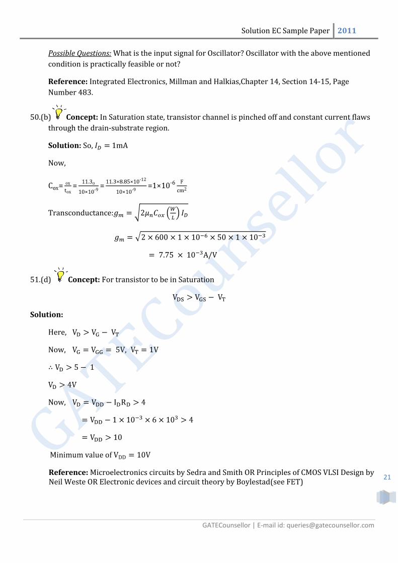
50.(b) Concept: In Saturation state, transistor channel is pinched off and constant current flaws
through the drain-substrate region.
Solution: So, 1mA
Now,
-
-
-
-
Transconductance:
A/V
51.(d) Concept: For transistor to be in Saturation
Solution:
Here,
Now,
Now,
Reference: Microelectronics circuits by Sedra and Smith OR Principles of CMOS VLSI Design by Neil Weste OR Electronic devices and circuit theory by Boylestad(see FET)
Solution EC Sample Paper 2011
GATECounsellor | E-mail id: [email protected]
22
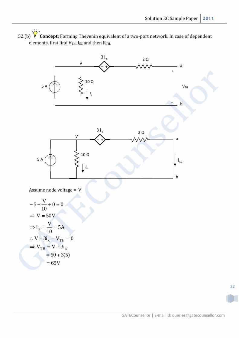
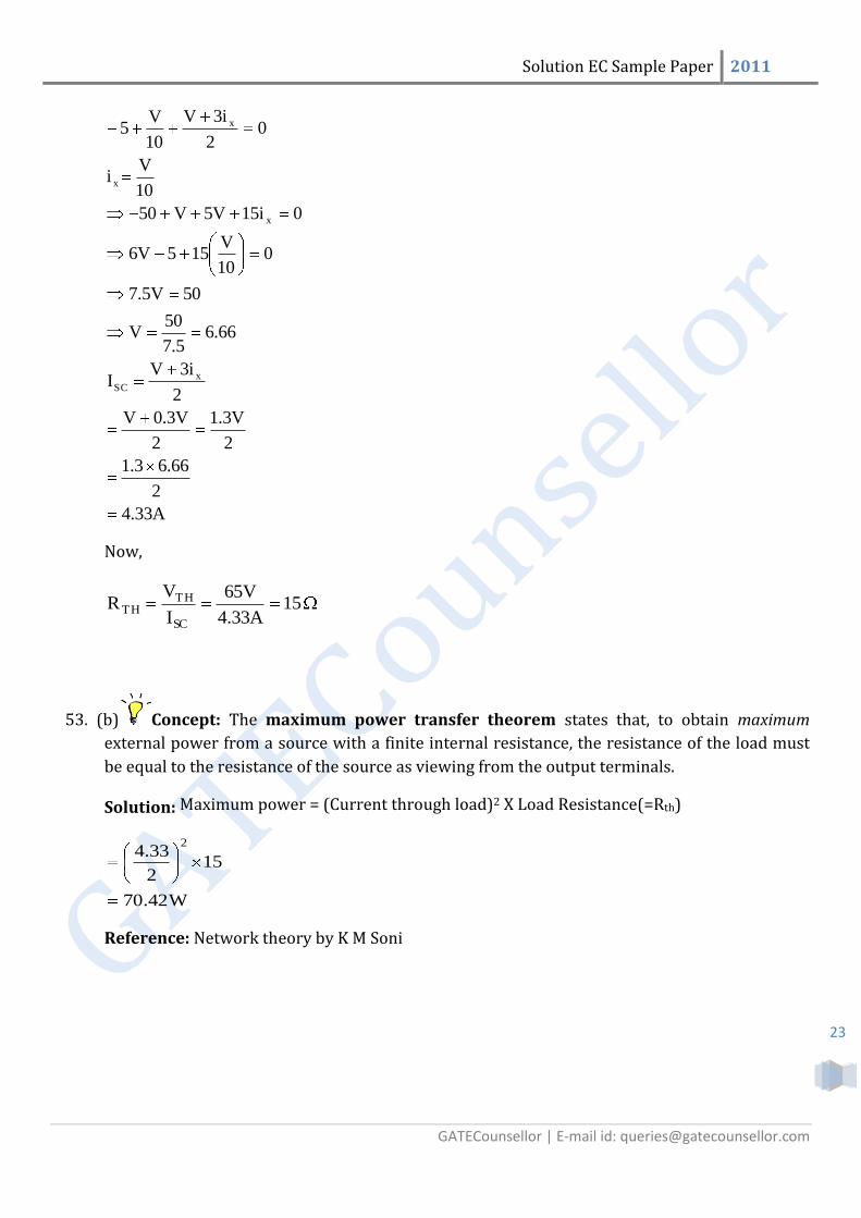
52.(b) Concept: Forming Thevenin equivalent of a two-port network. In case of dependent
elements, first find VTH, ISC and then RTH.
Assume node voltage = V
V65
)5(350
i3VV
0Vi3V
A510
Vi
V50V
0010
V5
xTH
THx
x
V
b
5 A 10 Ω
ix
xi3 2 Ω
a +
VTH
-
V
b
5 A 10 Ω
ix
xi3 2 Ω
a
Isc
Solution EC Sample Paper 2011
GATECounsellor | E-mail id: [email protected]
23
4.33A
2
6.661.3
2
1.3V
2
0.3VV
2
3iVI
6.667.5
50V
507.5V
010
V1556V
015i5VV50
10
Vi
02
3iV
10
V5
xSC
x
x
x
Now,
15A33.4
V65
I
VR
SC
THTH
53. (b) Concept: The maximum power transfer theorem states that, to obtain maximum
external power from a source with a finite internal resistance, the resistance of the load must
be equal to the resistance of the source as viewing from the output terminals.
Solution: Maximum power = (Current through load)2 X Load Resistance(=Rth)
W42.70
152
33.42
Reference: Network theory by K M Soni
Solution EC Sample Paper 2011
GATECounsellor | E-mail id: [email protected]
24
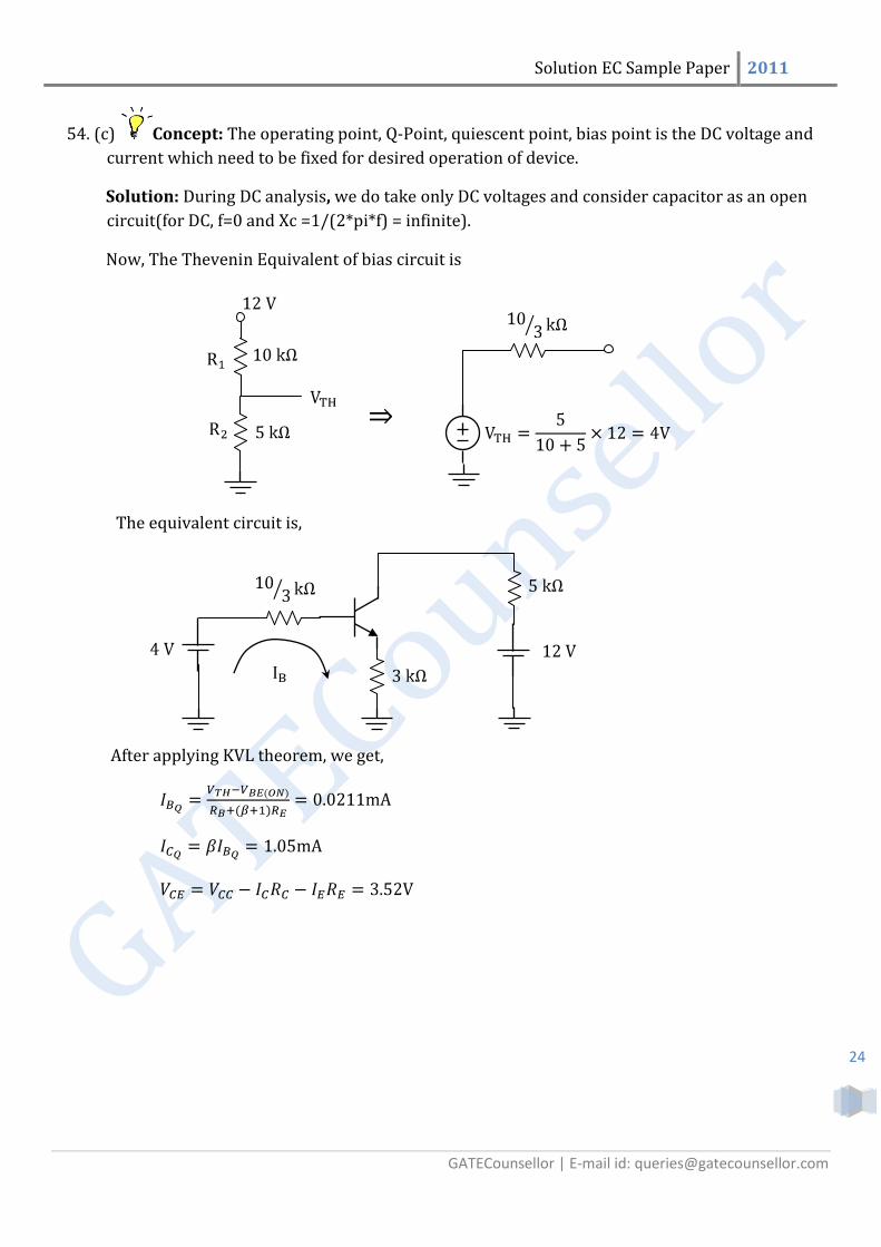
54. (c) Concept: The operating point, Q-Point, quiescent point, bias point is the DC voltage and
current which need to be fixed for desired operation of device.
Solution: During DC analysis, we do take only DC voltages and consider capacitor as an open
circuit(for DC, f=0 and Xc =1/(2*pi*f) = infinite).
Now, The Thevenin Equivalent of bias circuit is
The equivalent circuit is,
After applying KVL theorem, we get,
Solution EC Sample Paper 2011
GATECounsellor | E-mail id: [email protected]
25
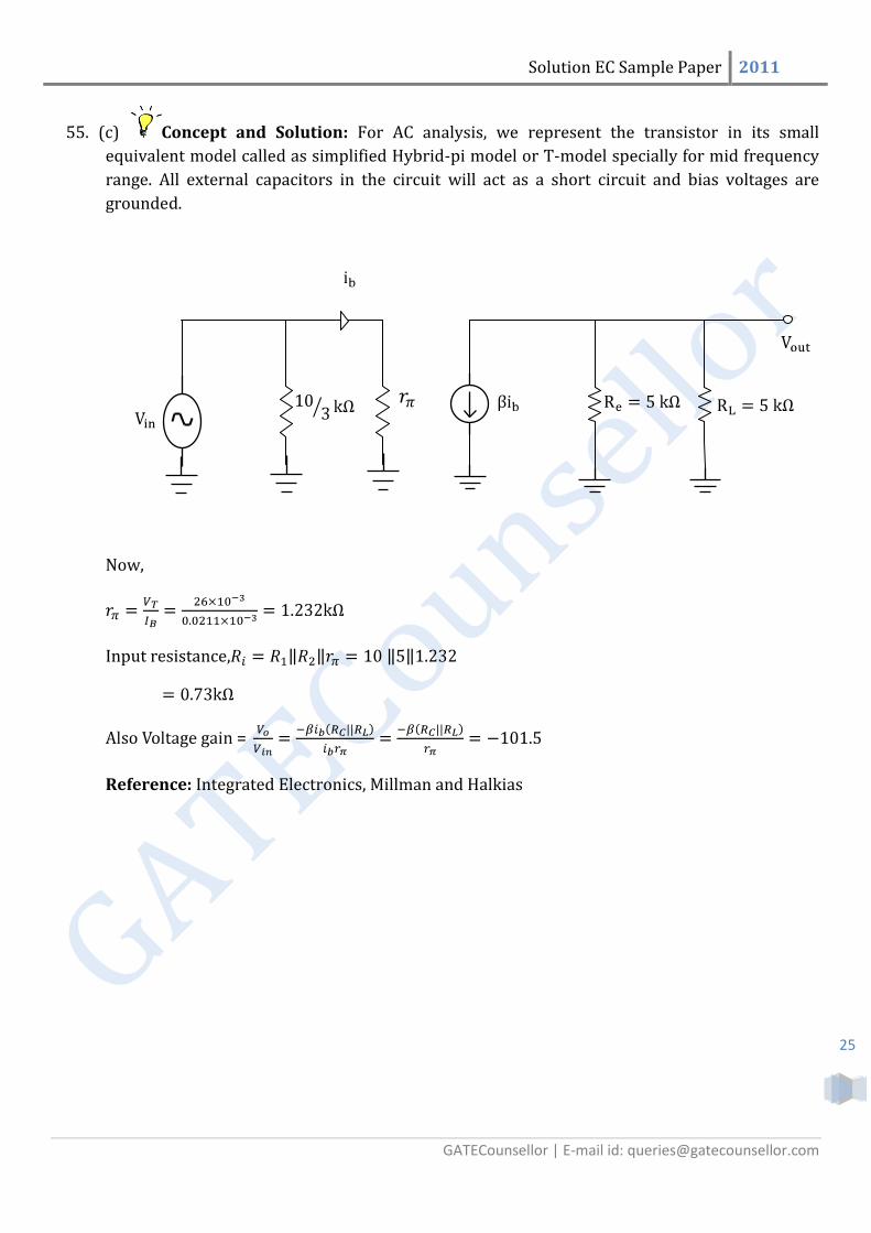
55. (c) Concept and Solution: For AC analysis, we represent the transistor in its small
equivalent model called as simplified Hybrid-pi model or T-model specially for mid frequency
range. All external capacitors in the circuit will act as a short circuit and bias voltages are
grounded.
Now,
Input resistance,
Reference: Integrated Electronics, Millman and Halkias
Related Documents


![EC-GATE-2011[1].pdf solution](https://static.cupdf.com/doc/110x72/551b65db4a795997718b46fb/ec-gate-20111pdf-solution.jpg)