OE 6 1 3 4 LE D C D Q Product Folder Order Now Technical Documents Tools & Software Support & Community An IMPORTANT NOTICE at the end of this data sheet addresses availability, warranty, changes, use in safety-critical applications, intellectual property matters and other important disclaimers. PRODUCTION DATA. SN74LVC1G373 SCES528F – DECEMBER 2003 – REVISED MAY 2017 SN74LVC1G373 Single D-Type Latch With 3-State Output 1 1 Features 1• Available in the Texas Instruments NanoFree™ Package • Supports 5-V V CC Operation • Inputs Accept Voltages to 5.5 V • Provides Down Translation to V CC • Max t pd of 4 ns at 3.3 V • Low Power Consumption: 10-μA Maximum I CC • ±24-mA Output Drive at 3.3 V • I off Supports Partial-Power-Down Mode and Back Drive Protection • Latch-Up Performance Exceeds 100 mA Per JESD 78, Class II 2 Applications • Servers • Printers • Telecom and Grid Infrastructure • Memory Addressing • Buffer Registers • Electronic Point of Sale 3 Description The SN74LVC1G373 device is a single D-type latch designed for 1.65-V to 5.5-V V CC operation. This device is particularly suitable for implementing buffer registers, I/O ports, bidirectional bus drivers, and working registers. While the latch-enable (LE) input is high, the Q outputs follow the data (D) inputs. When LE is taken low, the Q outputs are latched at the logic levels set up at the D inputs. NanoFree™ package technology is a major breakthrough in IC packaging concepts, using the die as the package. OE does not affect the internal operations of the latch. Old data can be retained or new data can be entered while the outputs are in the high-impedance state. Device Information(1) PACKAGE NUMBER PACKAGE BODY SIZE (NOM) SN74LVC1G373DBV SOT-23 (6) 2.90 mm × 1.60 mm SN74LVC1G373DCK SC70 (6) 2.00 mm × 1.25 mm SN74LVC1G373YZP DSBGA (6) 1.41 mm × 0.91 mm (1) For all available packages, see the orderable addendum at the end of the data sheet. Logic Diagram (Positive Logic)

Welcome message from author
This document is posted to help you gain knowledge. Please leave a comment to let me know what you think about it! Share it to your friends and learn new things together.
Transcript
OE6
1
3
4
LE
D
C
D
Q
Product
Folder
Order
Now
Technical
Documents
Tools &
Software
Support &Community
An IMPORTANT NOTICE at the end of this data sheet addresses availability, warranty, changes, use in safety-critical applications,intellectual property matters and other important disclaimers. PRODUCTION DATA.
SN74LVC1G373SCES528F –DECEMBER 2003–REVISED MAY 2017
SN74LVC1G373 Single D-Type Latch With 3-State Output
1
1 Features1• Available in the Texas Instruments
NanoFree™ Package• Supports 5-V VCC Operation• Inputs Accept Voltages to 5.5 V• Provides Down Translation to VCC
• Max tpd of 4 ns at 3.3 V• Low Power Consumption: 10-μA
Maximum ICC
• ±24-mA Output Drive at 3.3 V• Ioff Supports Partial-Power-Down Mode and Back
Drive Protection• Latch-Up Performance Exceeds 100 mA
Per JESD 78, Class II
2 Applications• Servers• Printers• Telecom and Grid Infrastructure• Memory Addressing• Buffer Registers• Electronic Point of Sale
3 DescriptionThe SN74LVC1G373 device is a single D-type latchdesigned for 1.65-V to 5.5-V VCC operation.
This device is particularly suitable for implementingbuffer registers, I/O ports, bidirectional bus drivers,and working registers. While the latch-enable (LE)input is high, the Q outputs follow the data (D) inputs.When LE is taken low, the Q outputs are latched atthe logic levels set up at the D inputs.
NanoFree™ package technology is a majorbreakthrough in IC packaging concepts, using the dieas the package.
OE does not affect the internal operations of thelatch. Old data can be retained or new data can beentered while the outputs are in the high-impedancestate.
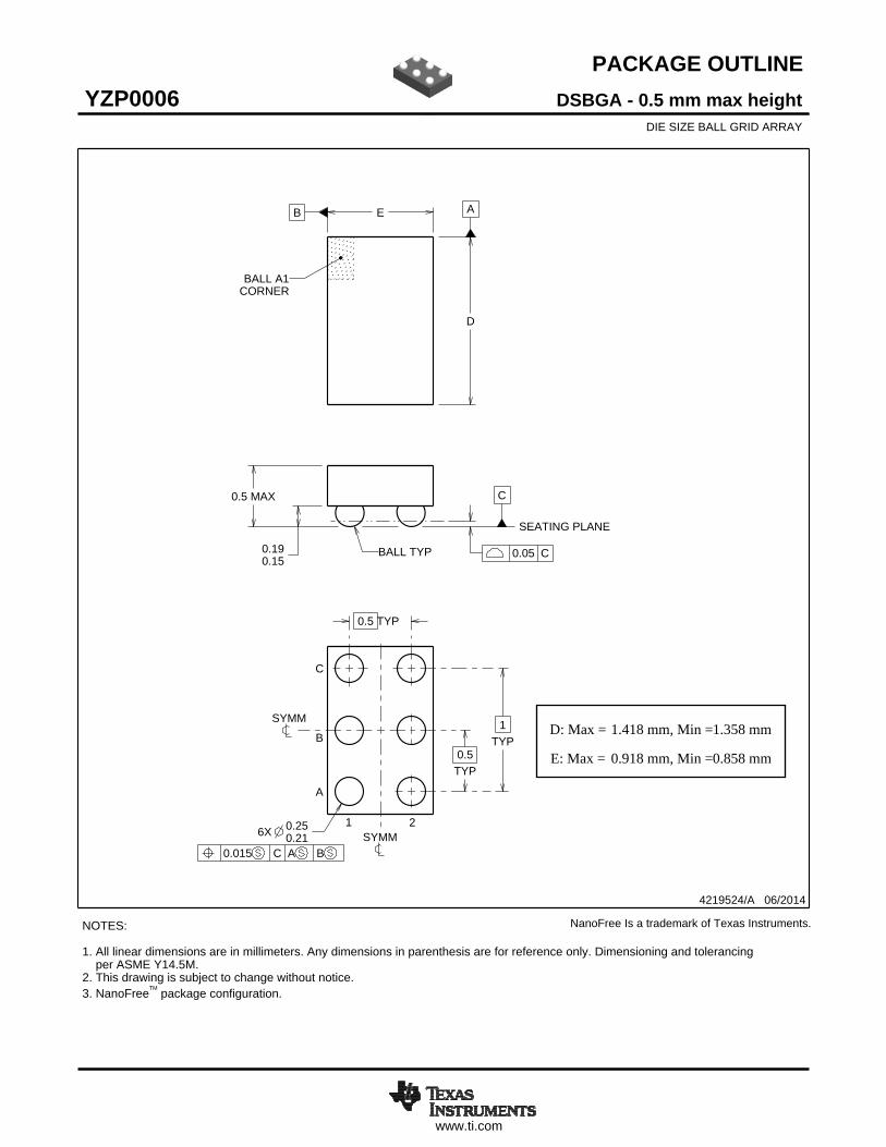
Device Information(1)PACKAGE NUMBER PACKAGE BODY SIZE (NOM)SN74LVC1G373DBV SOT-23 (6) 2.90 mm × 1.60 mmSN74LVC1G373DCK SC70 (6) 2.00 mm × 1.25 mmSN74LVC1G373YZP DSBGA (6) 1.41 mm × 0.91 mm
(1) For all available packages, see the orderable addendum atthe end of the data sheet.
Logic Diagram (Positive Logic)
2
SN74LVC1G373SCES528F –DECEMBER 2003–REVISED MAY 2017 www.ti.com
Product Folder Links: SN74LVC1G373
Submit Documentation Feedback Copyright © 2003–2017, Texas Instruments Incorporated
Table of Contents1 Features .................................................................. 12 Applications ........................................................... 13 Description ............................................................. 14 Revision History..................................................... 25 Pin Configuration and Functions ......................... 36 Specifications......................................................... 4
6.1 Absolute Maximum Ratings ...................................... 46.2 ESD Ratings.............................................................. 46.3 Recommended Operating Conditions....................... 56.4 Thermal Information .................................................. 56.5 Electrical Characteristics........................................... 66.6 Timing Requirements: TA = –40°C to +85°C ............ 66.7 Timing Requirements: TA = –40°C to +125°C .......... 66.8 Switching Characteristics: TA = –40°C to +85°C ...... 76.9 Switching Characteristics: TA = –40°C to +85°C ...... 76.10 Switching Characteristics: TA = –40°C to +125°C .. 86.11 Operating Characteristics........................................ 86.12 Typical Characteristics ............................................ 9
7 Parameter Measurement Information ................ 108 Detailed Description ............................................ 12
8.1 Overview ................................................................. 128.2 Functional Block Diagram ....................................... 128.3 Feature Description................................................. 128.4 Device Functional Modes........................................ 13
9 Application and Implementation ........................ 149.1 Application Information............................................ 149.2 Typical Application .................................................. 14
10 Power Supply Recommendations ..................... 1611 Layout................................................................... 16
11.1 Layout Guidelines ................................................. 1611.2 Layout Example .................................................... 16
12 Device and Documentation Support ................. 1712.1 Documentation Support ........................................ 1712.2 Receiving Notification of Documentation Updates 1712.3 Community Resource............................................ 1712.4 Trademarks ........................................................... 1712.5 Electrostatic Discharge Caution............................ 1712.6 Glossary ................................................................ 17
13 Mechanical, Packaging, and OrderableInformation ........................................................... 17
4 Revision HistoryNOTE: Page numbers for previous revisions may differ from page numbers in the current version.
Changes from Revision E (September 2016) to Revision F Page
• Changed YZP Package pinout diagram and added YZP pin numbers in Pin Functions table .............................................. 3• Added Balanced High-Drive CMOS Push-Pull Outputs, Standard CMOS Inputs, Clamp Diodes, Partial Power Down
(Ioff), Over-voltage Tolerant Inputs ........................................................................................................................................ 12• Added Trace Example in Layout Example section............................................................................................................... 16• Added Documentation Support section ................................................................................................................................ 17
Changes from Revision D (December 2013) to Revision E Page
• Added Applications section, Device Information table, ESD Ratings table, Feature Description section, DeviceFunctional Modes, Application and Implementation section, Power Supply Recommendations section, Layoutsection, Device and Documentation Support section, and Mechanical, Packaging, and Orderable Informationsection ................................................................................................................................................................................... 1
Changes from Revision C (May 2007) to Revision D Page
• Updated document to new TI data sheet format. ................................................................................................................... 1• Deleted Ordering Information table; see POA at the end of the data sheet........................................................................... 1• Updated operating temperature range. .................................................................................................................................. 5
1 2
C
B
A
Not to scale
D Q
GND VCC
LE OE
2GND VCC5
3 4D Q
61LE OE
3 4D
2GND
Q
5
1LE
VCC
6 OE
3
SN74LVC1G373www.ti.com SCES528F –DECEMBER 2003–REVISED MAY 2017
Product Folder Links: SN74LVC1G373
Submit Documentation FeedbackCopyright © 2003–2017, Texas Instruments Incorporated
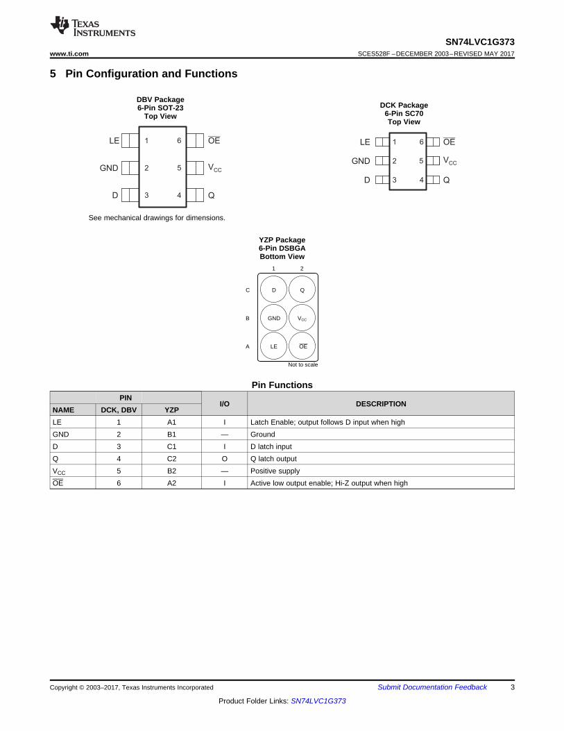
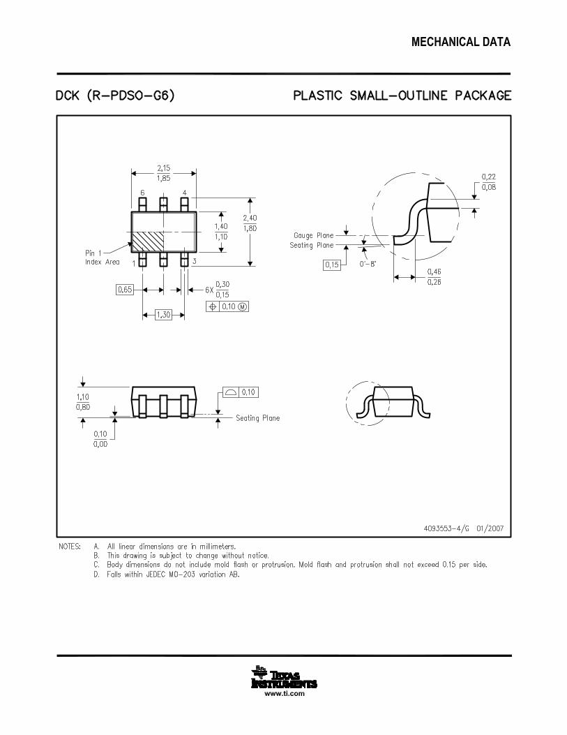
5 Pin Configuration and Functions
DBV Package6-Pin SOT-23
Top View
See mechanical drawings for dimensions.
DCK Package6-Pin SC70Top View
YZP Package6-Pin DSBGABottom View
Pin FunctionsPIN
I/O DESCRIPTIONNAME DCK, DBV YZPLE 1 A1 I Latch Enable; output follows D input when highGND 2 B1 — GroundD 3 C1 I D latch inputQ 4 C2 O Q latch outputVCC 5 B2 — Positive supplyOE 6 A2 I Active low output enable; Hi-Z output when high
4
SN74LVC1G373SCES528F –DECEMBER 2003–REVISED MAY 2017 www.ti.com
Product Folder Links: SN74LVC1G373
Submit Documentation Feedback Copyright © 2003–2017, Texas Instruments Incorporated
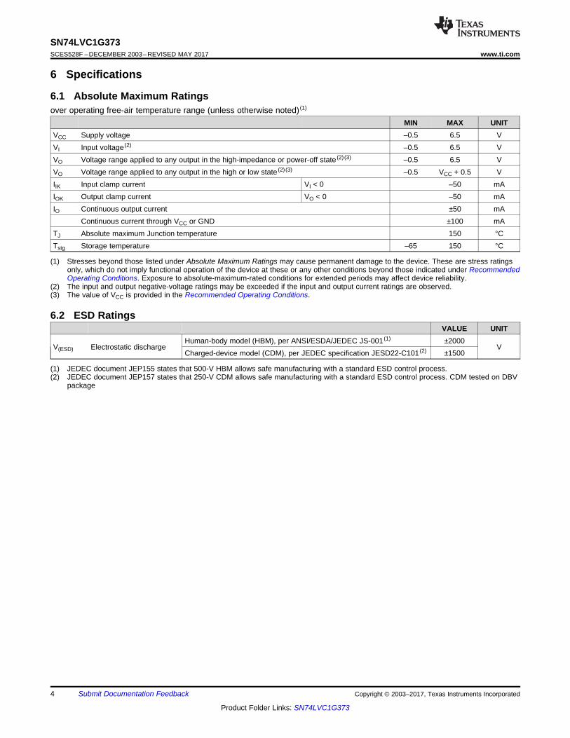
(1) Stresses beyond those listed under Absolute Maximum Ratings may cause permanent damage to the device. These are stress ratingsonly, which do not imply functional operation of the device at these or any other conditions beyond those indicated under RecommendedOperating Conditions. Exposure to absolute-maximum-rated conditions for extended periods may affect device reliability.
(2) The input and output negative-voltage ratings may be exceeded if the input and output current ratings are observed.(3) The value of VCC is provided in the Recommended Operating Conditions.
6 Specifications
6.1 Absolute Maximum Ratingsover operating free-air temperature range (unless otherwise noted) (1)
MIN MAX UNITVCC Supply voltage –0.5 6.5 VVI Input voltage (2) –0.5 6.5 VVO Voltage range applied to any output in the high-impedance or power-off state (2) (3) –0.5 6.5 VVO Voltage range applied to any output in the high or low state (2) (3) –0.5 VCC + 0.5 VIIK Input clamp current VI < 0 –50 mAIOK Output clamp current VO < 0 –50 mAIO Continuous output current ±50 mA
Continuous current through VCC or GND ±100 mATJ Absolute maximum Junction temperature 150 °CTstg Storage temperature –65 150 °C
(1) JEDEC document JEP155 states that 500-V HBM allows safe manufacturing with a standard ESD control process.(2) JEDEC document JEP157 states that 250-V CDM allows safe manufacturing with a standard ESD control process. CDM tested on DBV
package
6.2 ESD RatingsVALUE UNIT
V(ESD) Electrostatic dischargeHuman-body model (HBM), per ANSI/ESDA/JEDEC JS-001 (1) ±2000
VCharged-device model (CDM), per JEDEC specification JESD22-C101 (2) ±1500
5
SN74LVC1G373www.ti.com SCES528F –DECEMBER 2003–REVISED MAY 2017
Product Folder Links: SN74LVC1G373
Submit Documentation FeedbackCopyright © 2003–2017, Texas Instruments Incorporated
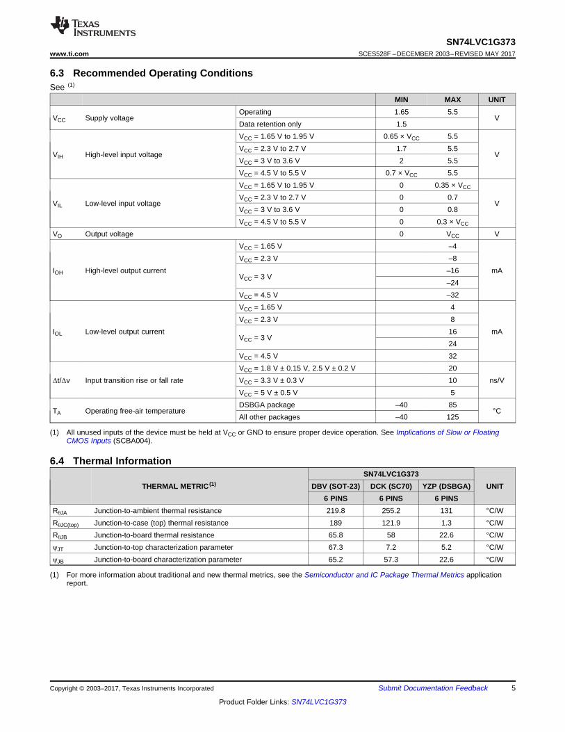
(1) All unused inputs of the device must be held at VCC or GND to ensure proper device operation. See Implications of Slow or FloatingCMOS Inputs (SCBA004).
6.3 Recommended Operating ConditionsSee (1)
MIN MAX UNIT
VCC Supply voltageOperating 1.65 5.5
VData retention only 1.5
VIH High-level input voltage
VCC = 1.65 V to 1.95 V 0.65 × VCC 5.5
VVCC = 2.3 V to 2.7 V 1.7 5.5VCC = 3 V to 3.6 V 2 5.5VCC = 4.5 V to 5.5 V 0.7 × VCC 5.5
VIL Low-level input voltage
VCC = 1.65 V to 1.95 V 0 0.35 × VCC
VVCC = 2.3 V to 2.7 V 0 0.7VCC = 3 V to 3.6 V 0 0.8VCC = 4.5 V to 5.5 V 0 0.3 × VCC
VO Output voltage 0 VCC V
IOH High-level output current
VCC = 1.65 V –4
mAVCC = 2.3 V –8
VCC = 3 V–16–24
VCC = 4.5 V –32
IOL Low-level output current
VCC = 1.65 V 4
mAVCC = 2.3 V 8
VCC = 3 V1624
VCC = 4.5 V 32
Δt/Δv Input transition rise or fall rateVCC = 1.8 V ± 0.15 V, 2.5 V ± 0.2 V 20
ns/VVCC = 3.3 V ± 0.3 V 10VCC = 5 V ± 0.5 V 5
TA Operating free-air temperatureDSBGA package –40 85
°CAll other packages –40 125
(1) For more information about traditional and new thermal metrics, see the Semiconductor and IC Package Thermal Metrics applicationreport.
6.4 Thermal Information
THERMAL METRIC (1)SN74LVC1G373
UNITDBV (SOT-23) DCK (SC70) YZP (DSBGA)6 PINS 6 PINS 6 PINS
RθJA Junction-to-ambient thermal resistance 219.8 255.2 131 °C/WRθJC(top) Junction-to-case (top) thermal resistance 189 121.9 1.3 °C/WRθJB Junction-to-board thermal resistance 65.8 58 22.6 °C/WψJT Junction-to-top characterization parameter 67.3 7.2 5.2 °C/WψJB Junction-to-board characterization parameter 65.2 57.3 22.6 °C/W
6
SN74LVC1G373SCES528F –DECEMBER 2003–REVISED MAY 2017 www.ti.com
Product Folder Links: SN74LVC1G373
Submit Documentation Feedback Copyright © 2003–2017, Texas Instruments Incorporated
(1) All typical values are at VCC = 3.3 V, TA = 25°C.
6.5 Electrical Characteristicsover recommended operating free-air temperature range (unless otherwise noted)
PARAMETER TEST CONDITIONS VCC MIN TYP (1) MAX UNIT
VOH
IOH = –100 µA 1.65 V to 5.5 V VCC – 0.1
V
IOH = –4 mA 1.65 V 1.2
IOH = –8 mA 2.3 V 1.9
IOH = –16 mA3 V
2.4
IOH = –24 mA 2.3
IOH = –32 mA 4.5 V 3.8
VOL
IOL = 100 µA 1.65 V to 5.5 V 0.1
V
IOL = 4 mA 1.65 V 0.45
IOL = 8 mA 2.3 V 0.3
IOL = 16 mA
3 V
0.4
IOL= 24 mATA = –40°C to 85°C 0.55
TA = –40°C to 125°C 0.65
IOL= 32 mATA = –40°C to 85°C
4.5 V0.55
TA = –40°C to 125°C 0.65
II VI = 5.5 V or GND 0 V to 5.5 V ±1
µA
IOZ VO = 0 to 5.5 V 3.6 V ±5
Ioff VI or VO = 5.5 V 0 ±10
ICC VI = 5.5 V or GND, IO = 0 1.65 V to 5.5 V 10
ΔICCOne input at VCC – 0.6 V,Other inputs at VCC or GND 3 V to 5.5 V 500
Ci VI = VCC or GND TA = –40°C to 85°C 3.3 V 3.5pF
Co VO = VCC or GND TA = –40°C to 85°C 3.3 V 6
6.6 Timing Requirements: TA = –40°C to +85°Cover recommended operating free-air temperature range (unless otherwise noted) (see Figure 2)
MIN MAX UNIT
tw Pulse duration, LE high 3
ns
tsu Setup time, data before LE↓
VCC = 1.8 V ± 0.15 V 2.4
VCC = 2.5 V ± 0.2 V 2
VCC = 3.3 V ± 0.3 V 1.5
VCC = 5 V ± 0.5 V 1.5
th Hold time, data after LE↓
VCC = 1.8 V ± 0.15 V 2.5
VCC = 2.5 V ± 0.2 V 1.5
VCC = 3.3 V ± 0.3 V 1.5
VCC = 5 V ± 0.5 V 1.5
6.7 Timing Requirements: TA = –40°C to +125°Cover recommended operating free-air temperature range (unless otherwise noted) (see Figure 2)
MIN MAX UNIT
tw Pulse duration, LE high 3
ns
tsu Setup time, data before LE↓
VCC = 1.8 V ± 0.15 V 2.9
VCC = 2.5 V ± 0.2 V 2.1
VCC = 3.3 V ± 0.3 V 1.5
VCC = 5 V ± 0.5 V 1.5
th Hold time, data after LE↓
VCC = 1.8 V ± 0.15 V 3
VCC = 2.5 V ± 0.2 V 1.5
VCC = 3.3 V ± 0.3 V 1.5
VCC = 5 V ± 0.5 V 1.5
7
SN74LVC1G373www.ti.com SCES528F –DECEMBER 2003–REVISED MAY 2017
Product Folder Links: SN74LVC1G373
Submit Documentation FeedbackCopyright © 2003–2017, Texas Instruments Incorporated
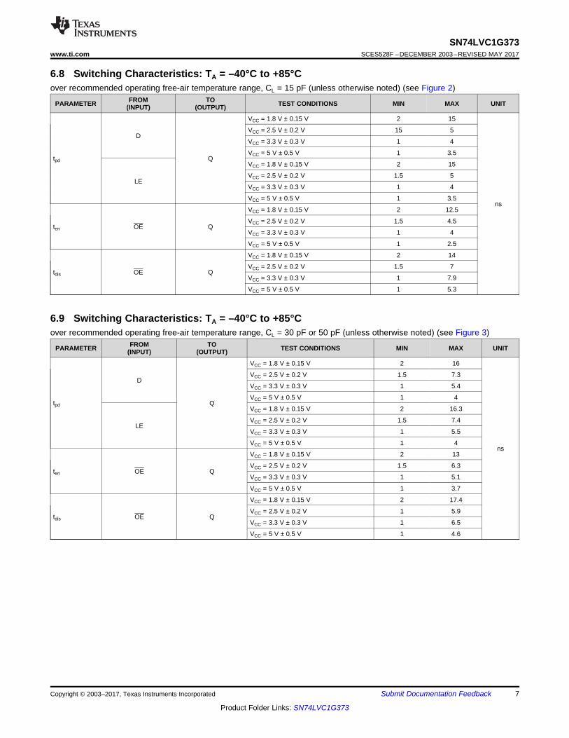
6.8 Switching Characteristics: TA = –40°C to +85°Cover recommended operating free-air temperature range, CL = 15 pF (unless otherwise noted) (see Figure 2)
PARAMETER FROM(INPUT)
TO(OUTPUT) TEST CONDITIONS MIN MAX UNIT
tpd
D
Q
VCC = 1.8 V ± 0.15 V 2 15
ns
VCC = 2.5 V ± 0.2 V 15 5
VCC = 3.3 V ± 0.3 V 1 4
VCC = 5 V ± 0.5 V 1 3.5
LE
VCC = 1.8 V ± 0.15 V 2 15
VCC = 2.5 V ± 0.2 V 1.5 5
VCC = 3.3 V ± 0.3 V 1 4
VCC = 5 V ± 0.5 V 1 3.5
ten OE Q
VCC = 1.8 V ± 0.15 V 2 12.5
VCC = 2.5 V ± 0.2 V 1.5 4.5
VCC = 3.3 V ± 0.3 V 1 4
VCC = 5 V ± 0.5 V 1 2.5
tdis OE Q
VCC = 1.8 V ± 0.15 V 2 14
VCC = 2.5 V ± 0.2 V 1.5 7
VCC = 3.3 V ± 0.3 V 1 7.9
VCC = 5 V ± 0.5 V 1 5.3
6.9 Switching Characteristics: TA = –40°C to +85°Cover recommended operating free-air temperature range, CL = 30 pF or 50 pF (unless otherwise noted) (see Figure 3)
PARAMETER FROM(INPUT)
TO(OUTPUT) TEST CONDITIONS MIN MAX UNIT
tpd
D
Q
VCC = 1.8 V ± 0.15 V 2 16
ns
VCC = 2.5 V ± 0.2 V 1.5 7.3
VCC = 3.3 V ± 0.3 V 1 5.4
VCC = 5 V ± 0.5 V 1 4
LE
VCC = 1.8 V ± 0.15 V 2 16.3
VCC = 2.5 V ± 0.2 V 1.5 7.4
VCC = 3.3 V ± 0.3 V 1 5.5
VCC = 5 V ± 0.5 V 1 4
ten OE Q
VCC = 1.8 V ± 0.15 V 2 13
VCC = 2.5 V ± 0.2 V 1.5 6.3
VCC = 3.3 V ± 0.3 V 1 5.1
VCC = 5 V ± 0.5 V 1 3.7
tdis OE Q
VCC = 1.8 V ± 0.15 V 2 17.4
VCC = 2.5 V ± 0.2 V 1 5.9
VCC = 3.3 V ± 0.3 V 1 6.5
VCC = 5 V ± 0.5 V 1 4.6
8
SN74LVC1G373SCES528F –DECEMBER 2003–REVISED MAY 2017 www.ti.com
Product Folder Links: SN74LVC1G373
Submit Documentation Feedback Copyright © 2003–2017, Texas Instruments Incorporated
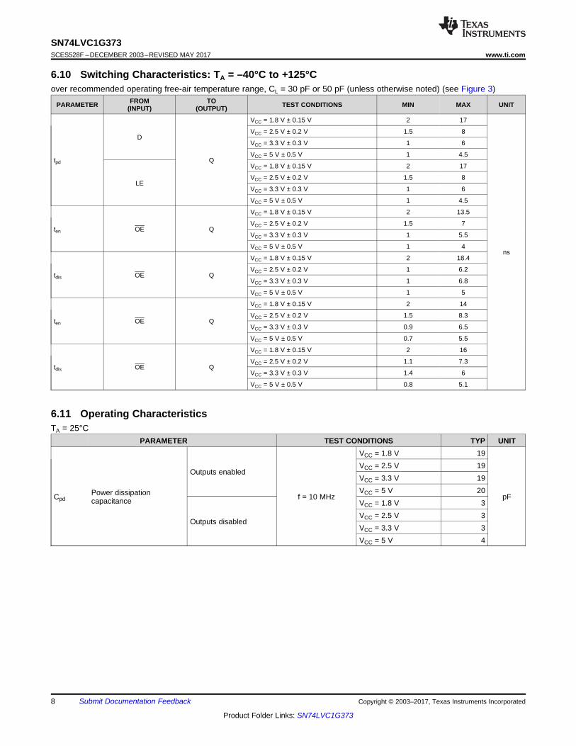
6.10 Switching Characteristics: TA = –40°C to +125°Cover recommended operating free-air temperature range, CL = 30 pF or 50 pF (unless otherwise noted) (see Figure 3)
PARAMETER FROM(INPUT)
TO(OUTPUT) TEST CONDITIONS MIN MAX UNIT
tpd
D
Q
VCC = 1.8 V ± 0.15 V 2 17
ns
VCC = 2.5 V ± 0.2 V 1.5 8
VCC = 3.3 V ± 0.3 V 1 6
VCC = 5 V ± 0.5 V 1 4.5
LE
VCC = 1.8 V ± 0.15 V 2 17
VCC = 2.5 V ± 0.2 V 1.5 8
VCC = 3.3 V ± 0.3 V 1 6
VCC = 5 V ± 0.5 V 1 4.5
ten OE Q
VCC = 1.8 V ± 0.15 V 2 13.5
VCC = 2.5 V ± 0.2 V 1.5 7
VCC = 3.3 V ± 0.3 V 1 5.5
VCC = 5 V ± 0.5 V 1 4
tdis OE Q
VCC = 1.8 V ± 0.15 V 2 18.4
VCC = 2.5 V ± 0.2 V 1 6.2
VCC = 3.3 V ± 0.3 V 1 6.8
VCC = 5 V ± 0.5 V 1 5
ten OE Q
VCC = 1.8 V ± 0.15 V 2 14
VCC = 2.5 V ± 0.2 V 1.5 8.3
VCC = 3.3 V ± 0.3 V 0.9 6.5
VCC = 5 V ± 0.5 V 0.7 5.5
tdis OE Q
VCC = 1.8 V ± 0.15 V 2 16
VCC = 2.5 V ± 0.2 V 1.1 7.3
VCC = 3.3 V ± 0.3 V 1.4 6
VCC = 5 V ± 0.5 V 0.8 5.1
6.11 Operating CharacteristicsTA = 25°C
PARAMETER TEST CONDITIONS TYP UNIT
CpdPower dissipationcapacitance
Outputs enabled
f = 10 MHz
VCC = 1.8 V 19
pF
VCC = 2.5 V 19VCC = 3.3 V 19VCC = 5 V 20
Outputs disabled
VCC = 1.8 V 3VCC = 2.5 V 3VCC = 3.3 V 3VCC = 5 V 4
VCC (V)
TP
DM
ax (
ns)
1.5 2 2.5 3 3.5 4 4.5 52
4
6
8
10
12
14
16
D001
CL 30pF/50pFCL 15pF
9
SN74LVC1G373www.ti.com SCES528F –DECEMBER 2003–REVISED MAY 2017
Product Folder Links: SN74LVC1G373
Submit Documentation FeedbackCopyright © 2003–2017, Texas Instruments Incorporated
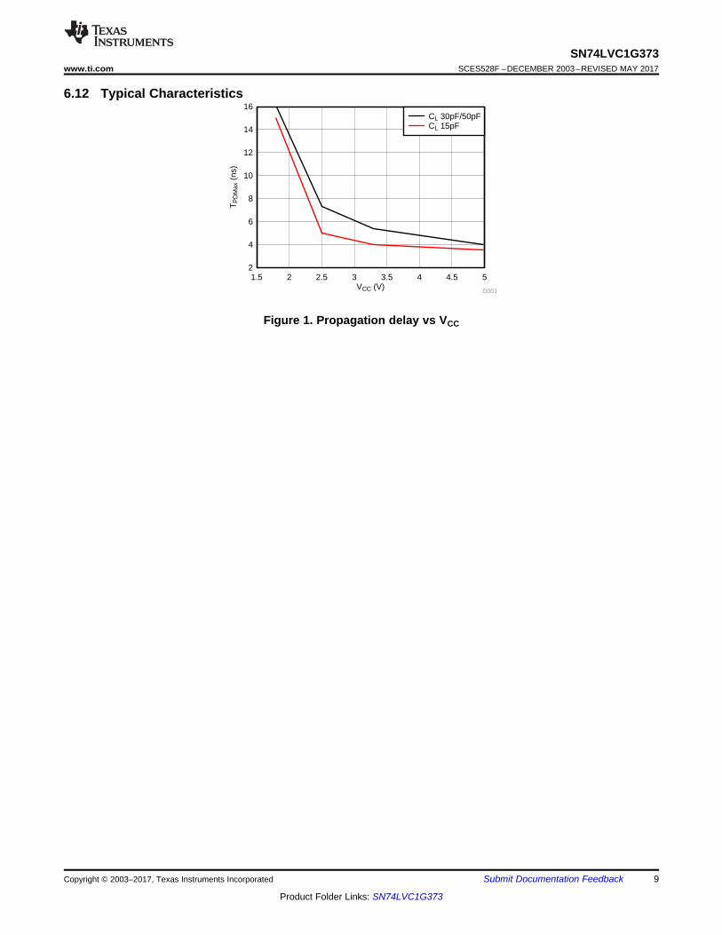
6.12 Typical Characteristics
Figure 1. Propagation delay vs VCC
thtsu
From OutputUnder Test
C
(see Note A)L
LOAD CIRCUIT
S1
VLOAD
Open
GND
RL
Data Input
Timing Input
0 V
0 V0 V
tW
Input
0 VInput
OutputWaveform 1
S1 at V
(see Note B)LOAD
OutputWaveform 2
S1 at GND(see Note B)
VOL
VOH
0 V
»0 V
Output
Output
t /tPLH PHL Open
TEST S1
OutputControl
VM
VM VM
VM
VM
1.8 V 0.15 V±
2.5 V 0.2 V±
3.3 V 0.3 V±
5 V 0.5 V±
1 MW
1 MW
1 MW
1 MW
VCC RL
2 × VCC
2 × VCC
6 V
2 × VCC
VLOAD CL
15 pF
15 pF
15 pF
15 pF
0.15 V
0.15 V
0.3 V
0.3 V
VD
3 V
VI
VCC/2
VCC/2
1.5 V
VCC/2
VM
£2 ns
£2 ns
£2.5 ns
£2.5 ns
INPUTS
RL
t /tr f
VCC
VCC
VCC
VLOADt /tPLZ PZL
GNDt /tPHZ PZH
VOLTAGE WAVEFORMSENABLE AND DISABLE TIMES
LOW- AND HIGH-LEVEL ENABLING
VOLTAGE WAVEFORMSPROPAGATION DELAY TIMES
INVERTING AND NONINVERTING OUTPUTS
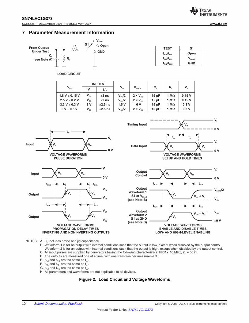
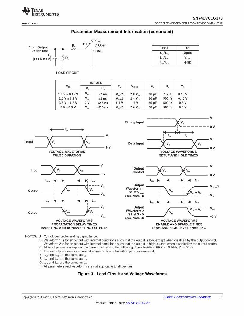
NOTES: A. C includes probe and jig capacitance.
B. Waveform 1 is for an output with internal conditions such that the output is low, except when disabled by the output control.Waveform 2 is for an output with internal conditions such that the output is high, except when disabled by the output control.
C. All input pulses are supplied by generators having the following characteristics: PRR 10 MHz, Z = 50 .
D. The outputs are measured one at a time, with one transition per measurement.E. t and t are the same as t .
F. t and t are the same as t .
G. t and t are the same as t .
H. All parameters and waveforms are not applicable to all devices.
L
O
PLZ PHZ dis
PZL PZH en
PLH PHL pd
£ W
VOLTAGE WAVEFORMSPULSE DURATION
VOLTAGE WAVEFORMSSETUP AND HOLD TIMES
VI
VI
VI
VM
VM
V /2LOAD
tPZL tPLZ
tPHZtPZH
V – VOH D
V + VOL D
VM
VM VM
VM
VOL
VOH
VI
VI
VOH
VOL
VM
VM
VM
VM
tPLH tPHL
tPLHtPHL
10
SN74LVC1G373SCES528F –DECEMBER 2003–REVISED MAY 2017 www.ti.com
Product Folder Links: SN74LVC1G373
Submit Documentation Feedback Copyright © 2003–2017, Texas Instruments Incorporated
7 Parameter Measurement Information
Figure 2. Load Circuit and Voltage Waveforms
thtsu
From OutputUnder Test
C
(see Note A)L
LOAD CIRCUIT
S1
VLOAD
Open
GND
RL
Data Input
Timing Input
0 V
0 V0 V
tW
Input
0 VInput
OutputWaveform 1
S1 at V
(see Note B)LOAD
OutputWaveform 2
S1 at GND(see Note B)
VOL
VOH
0 V
»0 V
Output
Output
TEST S1
t /tPLH PHL Open
OutputControl
VM
VM VM
VM
VM
1.8 V 0.15 V±
2.5 V 0.2 V±
3.3 V 0.3 V±
5 V 0.5 V±
1 kW
500 W
500 W
500 W
VCC RL
2 × VCC
2 × VCC
6 V
2 × VCC
VLOAD CL
30 pF
30 pF
50 pF
50 pF
0.15 V
0.15 V
0.3 V
0.3 V
VD
3 V
VI
VCC/2
VCC/2
1.5 V
VCC/2
VM
£2 ns
£2 ns
£2.5 ns
£2.5 ns
INPUTS
RL
t /tr f
VCC
VCC
VCC
VLOADt /tPLZ PZL
GNDt /tPHZ PZH
VOLTAGE WAVEFORMSENABLE AND DISABLE TIMES
LOW- AND HIGH-LEVEL ENABLING
VOLTAGE WAVEFORMSPROPAGATION DELAY TIMES
INVERTING AND NONINVERTING OUTPUTS
NOTES: A. C includes probe and jig capacitance.
B. Waveform 1 is for an output with internal conditions such that the output is low, except when disabled by the output control.Waveform 2 is for an output with internal conditions such that the output is high, except when disabled by the output control.
C. All input pulses are supplied by generators having the following characteristics: PRR 10 MHz, Z = 50 .
D. The outputs are measured one at a time, with one transition per measurement.E. t and t are the same as t .
F. t and t are the same as t .
G. t and t are the same as t .
H. All parameters and waveforms are not applicable to all devices.
L
O
PLZ PHZ dis
PZL PZH en
PLH PHL pd
£ W
VOLTAGE WAVEFORMSPULSE DURATION
VOLTAGE WAVEFORMSSETUP AND HOLD TIMES
VI
VI
VI
VM
VM
V /2LOAD
tPZL tPLZ
tPHZtPZH
V – VOH D
V + VOL D
VM
VM VM
VM
VOL
VOH
VI
VI
VOH
VOL
VM
VM
VM
VM
tPLH tPHL
tPLHtPHL
11
SN74LVC1G373www.ti.com SCES528F –DECEMBER 2003–REVISED MAY 2017
Product Folder Links: SN74LVC1G373
Submit Documentation FeedbackCopyright © 2003–2017, Texas Instruments Incorporated
Parameter Measurement Information (continued)
Figure 3. Load Circuit and Voltage Waveforms
OE6
1
3
4
LE
D
C
D
Q
12
SN74LVC1G373SCES528F –DECEMBER 2003–REVISED MAY 2017 www.ti.com
Product Folder Links: SN74LVC1G373
Submit Documentation Feedback Copyright © 2003–2017, Texas Instruments Incorporated
8 Detailed Description
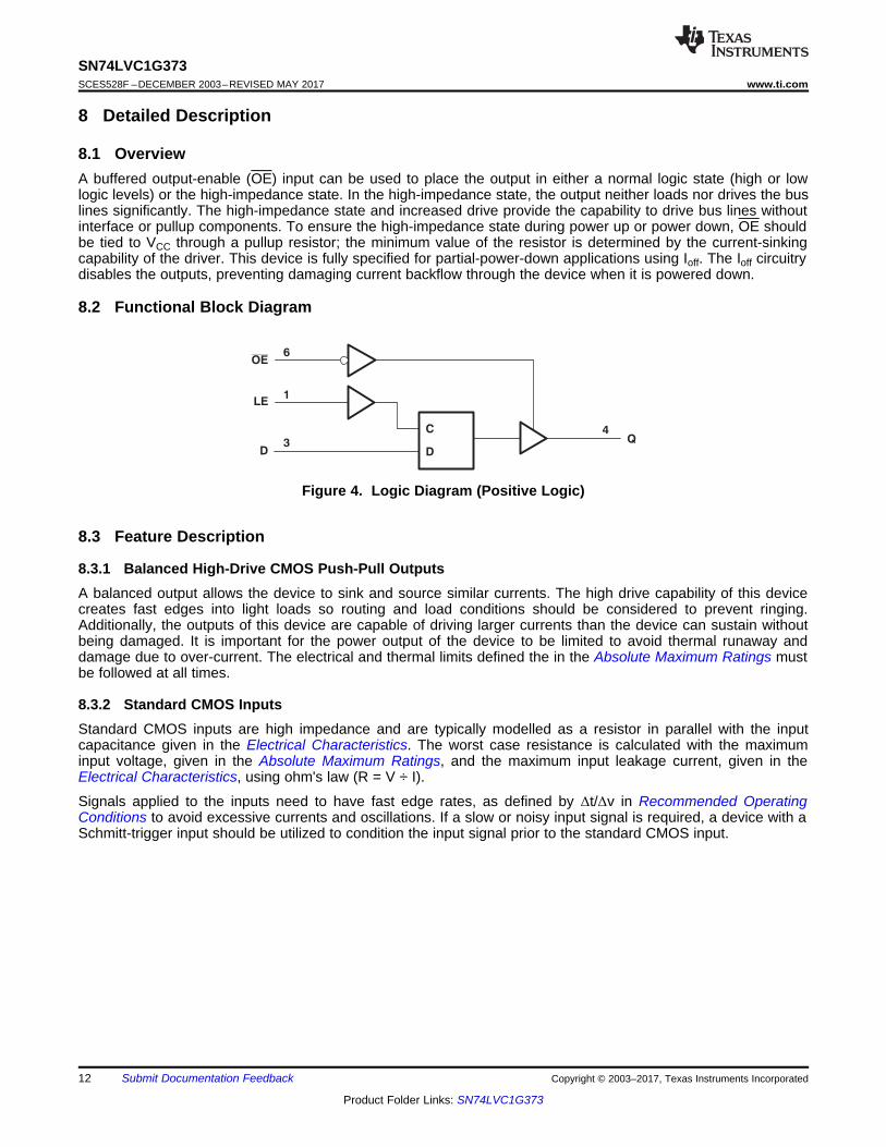
8.1 OverviewA buffered output-enable (OE) input can be used to place the output in either a normal logic state (high or lowlogic levels) or the high-impedance state. In the high-impedance state, the output neither loads nor drives the buslines significantly. The high-impedance state and increased drive provide the capability to drive bus lines withoutinterface or pullup components. To ensure the high-impedance state during power up or power down, OE shouldbe tied to VCC through a pullup resistor; the minimum value of the resistor is determined by the current-sinkingcapability of the driver. This device is fully specified for partial-power-down applications using Ioff. The Ioff circuitrydisables the outputs, preventing damaging current backflow through the device when it is powered down.
8.2 Functional Block Diagram
Figure 4. Logic Diagram (Positive Logic)
8.3 Feature Description
8.3.1 Balanced High-Drive CMOS Push-Pull OutputsA balanced output allows the device to sink and source similar currents. The high drive capability of this devicecreates fast edges into light loads so routing and load conditions should be considered to prevent ringing.Additionally, the outputs of this device are capable of driving larger currents than the device can sustain withoutbeing damaged. It is important for the power output of the device to be limited to avoid thermal runaway anddamage due to over-current. The electrical and thermal limits defined the in the Absolute Maximum Ratings mustbe followed at all times.
8.3.2 Standard CMOS InputsStandard CMOS inputs are high impedance and are typically modelled as a resistor in parallel with the inputcapacitance given in the Electrical Characteristics. The worst case resistance is calculated with the maximuminput voltage, given in the Absolute Maximum Ratings, and the maximum input leakage current, given in theElectrical Characteristics, using ohm's law (R = V ÷ I).
Signals applied to the inputs need to have fast edge rates, as defined by Δt/Δv in Recommended OperatingConditions to avoid excessive currents and oscillations. If a slow or noisy input signal is required, a device with aSchmitt-trigger input should be utilized to condition the input signal prior to the standard CMOS input.
GND
LogicInput Output
VCCDevice
-IIK -IOK
13
SN74LVC1G373www.ti.com SCES528F –DECEMBER 2003–REVISED MAY 2017
Product Folder Links: SN74LVC1G373
Submit Documentation FeedbackCopyright © 2003–2017, Texas Instruments Incorporated
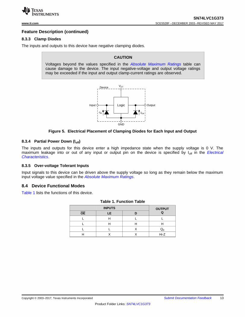
Feature Description (continued)8.3.3 Clamp DiodesThe inputs and outputs to this device have negative clamping diodes.
CAUTIONVoltages beyond the values specified in the Absolute Maximum Ratings table cancause damage to the device. The input negative-voltage and output voltage ratingsmay be exceeded if the input and output clamp-current ratings are observed.
Figure 5. Electrical Placement of Clamping Diodes for Each Input and Output
8.3.4 Partial Power Down (Ioff)The inputs and outputs for this device enter a high impedance state when the supply voltage is 0 V. Themaximum leakage into or out of any input or output pin on the device is specified by Ioff in the ElectricalCharacteristics.
8.3.5 Over-voltage Tolerant InputsInput signals to this device can be driven above the supply voltage so long as they remain below the maximuminput voltage value specified in the Absolute Maximum Ratings.
8.4 Device Functional ModesTable 1 lists the functions of this device.
Table 1. Function TableINPUTS OUTPUT
QOE LE DL H L LL H H HL L X Q0
H X X Hi-Z
LE Q
D
LE Q
D
1
8
A B C
COM
Y0
Y7
SN74LV4051A
Serial output
Live Data
Trigger Event
Copyright © 2016, Texas Instruments Incorporated
14
SN74LVC1G373SCES528F –DECEMBER 2003–REVISED MAY 2017 www.ti.com
Product Folder Links: SN74LVC1G373
Submit Documentation Feedback Copyright © 2003–2017, Texas Instruments Incorporated
9 Application and Implementation
NOTEInformation in the following applications sections is not part of the TI componentspecification, and TI does not warrant its accuracy or completeness. TI’s customers areresponsible for determining suitability of components for their purposes. Customers shouldvalidate and test their design implementation to confirm system functionality.
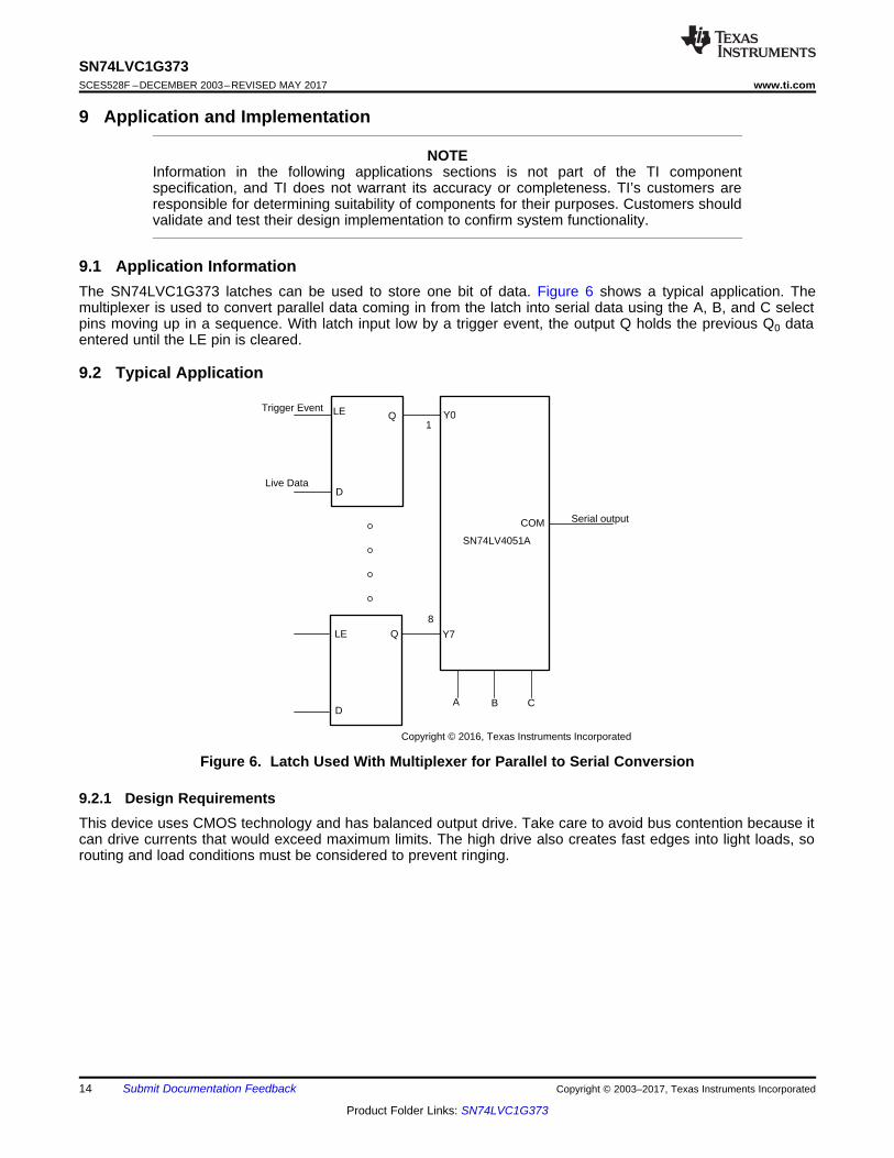
9.1 Application InformationThe SN74LVC1G373 latches can be used to store one bit of data. Figure 6 shows a typical application. Themultiplexer is used to convert parallel data coming in from the latch into serial data using the A, B, and C selectpins moving up in a sequence. With latch input low by a trigger event, the output Q holds the previous Q0 dataentered until the LE pin is cleared.
9.2 Typical Application
Figure 6. Latch Used With Multiplexer for Parallel to Serial Conversion
9.2.1 Design RequirementsThis device uses CMOS technology and has balanced output drive. Take care to avoid bus contention because itcan drive currents that would exceed maximum limits. The high drive also creates fast edges into light loads, sorouting and load conditions must be considered to prevent ringing.
VCC (V)
t EN
Max
(ns)
1.5 2 2.5 3 3.5 4 4.5 52
4
6
8
10
12
14
D001
CL30pF/50pFCL15pF
15
SN74LVC1G373www.ti.com SCES528F –DECEMBER 2003–REVISED MAY 2017
Product Folder Links: SN74LVC1G373
Submit Documentation FeedbackCopyright © 2003–2017, Texas Instruments Incorporated
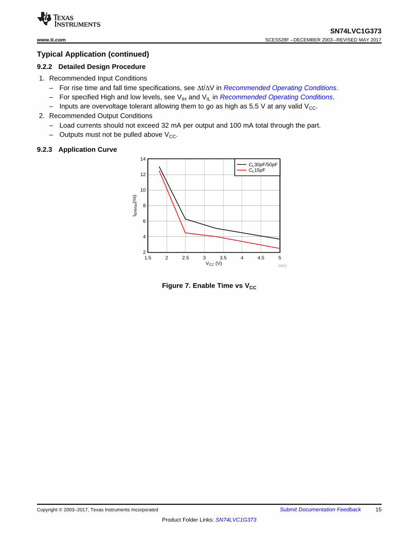
Typical Application (continued)9.2.2 Detailed Design Procedure1. Recommended Input Conditions
– For rise time and fall time specifications, see Δt/ΔV in Recommended Operating Conditions.– For specified High and low levels, see VIH and VIL in Recommended Operating Conditions.– Inputs are overvoltage tolerant allowing them to go as high as 5.5 V at any valid VCC.
2. Recommended Output Conditions– Load currents should not exceed 32 mA per output and 100 mA total through the part.– Outputs must not be pulled above VCC.
9.2.3 Application Curve
Figure 7. Enable Time vs VCC
WORST BETTER BEST
1W min.
W
2W
Vcc
Unused Input
Input
Output
Input
Unused Input Output
16
SN74LVC1G373SCES528F –DECEMBER 2003–REVISED MAY 2017 www.ti.com
Product Folder Links: SN74LVC1G373
Submit Documentation Feedback Copyright © 2003–2017, Texas Instruments Incorporated
10 Power Supply RecommendationsThe power supply can be any voltage between the minimum and maximum supply voltage rating located inRecommended Operating Conditions.
Each VCC pin should have a good bypass capacitor to prevent power disturbance. For devices with a singlesupply, TI recommends a 0.1-µF bypass capacitor. If there are multiple VCC pins, TI recommends 0.01-µF or0.022-µF bypass capacitor for each power pin. It is acceptable to parallel multiple bypass capacitors to rejectdifferent frequencies of noise. 0.1-µF and 1-µF capacitors are commonly used in parallel. The bypass capacitorshould be installed as close to the power pin as possible for best results.
11 Layout
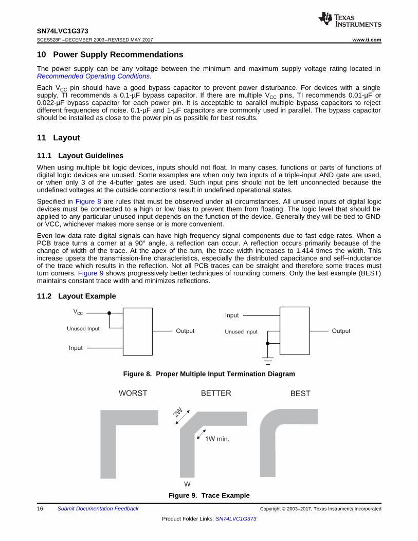
11.1 Layout GuidelinesWhen using multiple bit logic devices, inputs should not float. In many cases, functions or parts of functions ofdigital logic devices are unused. Some examples are when only two inputs of a triple-input AND gate are used,or when only 3 of the 4-buffer gates are used. Such input pins should not be left unconnected because theundefined voltages at the outside connections result in undefined operational states.
Specified in Figure 8 are rules that must be observed under all circumstances. All unused inputs of digital logicdevices must be connected to a high or low bias to prevent them from floating. The logic level that should beapplied to any particular unused input depends on the function of the device. Generally they will be tied to GNDor VCC, whichever makes more sense or is more convenient.
Even low data rate digital signals can have high frequency signal components due to fast edge rates. When aPCB trace turns a corner at a 90° angle, a reflection can occur. A reflection occurs primarily because of thechange of width of the trace. At the apex of the turn, the trace width increases to 1.414 times the width. Thisincrease upsets the transmission-line characteristics, especially the distributed capacitance and self–inductanceof the trace which results in the reflection. Not all PCB traces can be straight and therefore some traces mustturn corners. Figure 9 shows progressively better techniques of rounding corners. Only the last example (BEST)maintains constant trace width and minimizes reflections.
11.2 Layout Example
Figure 8. Proper Multiple Input Termination Diagram
Figure 9. Trace Example
17
SN74LVC1G373www.ti.com SCES528F –DECEMBER 2003–REVISED MAY 2017
Product Folder Links: SN74LVC1G373
Submit Documentation FeedbackCopyright © 2003–2017, Texas Instruments Incorporated
12 Device and Documentation Support
12.1 Documentation Support
12.1.1 Related DocumentationFor related documentation see the following:
Implications of Slow or Floating CMOS Inputs (SCBA004)
12.2 Receiving Notification of Documentation UpdatesTo receive notification of documentation updates, navigate to the device product folder on ti.com. In the upperright corner, click on Alert me to register and receive a weekly digest of any product information that haschanged. For change details, review the revision history included in any revised document.
12.3 Community ResourceThe following links connect to TI community resources. Linked contents are provided "AS IS" by the respectivecontributors. They do not constitute TI specifications and do not necessarily reflect TI's views; see TI's Terms ofUse.
TI E2E™ Online Community TI's Engineer-to-Engineer (E2E) Community. Created to foster collaborationamong engineers. At e2e.ti.com, you can ask questions, share knowledge, explore ideas and helpsolve problems with fellow engineers.
Design Support TI's Design Support Quickly find helpful E2E forums along with design support tools andcontact information for technical support.
12.4 TrademarksNanoFree, E2E are trademarks of Texas Instruments.All other trademarks are the property of their respective owners.
12.5 Electrostatic Discharge CautionThese devices have limited built-in ESD protection. The leads should be shorted together or the device placed in conductive foamduring storage or handling to prevent electrostatic damage to the MOS gates.
12.6 GlossarySLYZ022 — TI Glossary.
This glossary lists and explains terms, acronyms, and definitions.
13 Mechanical, Packaging, and Orderable InformationThe following pages include mechanical, packaging, and orderable information. This information is the mostcurrent data available for the designated devices. This data is subject to change without notice and revision ofthis document. For browser-based versions of this data sheet, refer to the left-hand navigation.
PACKAGE OPTION ADDENDUM
www.ti.com 28-Aug-2018
Addendum-Page 1
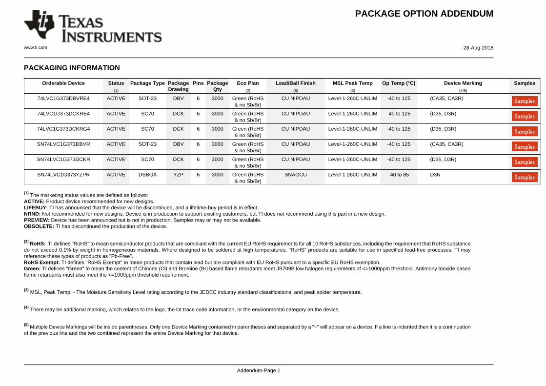
PACKAGING INFORMATION
Orderable Device Status(1)
Package Type PackageDrawing
Pins PackageQty
Eco Plan(2)
Lead/Ball Finish(6)
MSL Peak Temp(3)
Op Temp (°C) Device Marking(4/5)
Samples
74LVC1G373DBVRE4 ACTIVE SOT-23 DBV 6 3000 Green (RoHS& no Sb/Br)
CU NIPDAU Level-1-260C-UNLIM -40 to 125 (CA35, CA3R)
74LVC1G373DCKRE4 ACTIVE SC70 DCK 6 3000 Green (RoHS& no Sb/Br)
CU NIPDAU Level-1-260C-UNLIM -40 to 125 (D35, D3R)
74LVC1G373DCKRG4 ACTIVE SC70 DCK 6 3000 Green (RoHS& no Sb/Br)
CU NIPDAU Level-1-260C-UNLIM -40 to 125 (D35, D3R)
SN74LVC1G373DBVR ACTIVE SOT-23 DBV 6 3000 Green (RoHS& no Sb/Br)
CU NIPDAU Level-1-260C-UNLIM -40 to 125 (CA35, CA3R)
SN74LVC1G373DCKR ACTIVE SC70 DCK 6 3000 Green (RoHS& no Sb/Br)
CU NIPDAU Level-1-260C-UNLIM -40 to 125 (D35, D3R)
SN74LVC1G373YZPR ACTIVE DSBGA YZP 6 3000 Green (RoHS& no Sb/Br)
SNAGCU Level-1-260C-UNLIM -40 to 85 D3N
(1) The marketing status values are defined as follows:ACTIVE: Product device recommended for new designs.LIFEBUY: TI has announced that the device will be discontinued, and a lifetime-buy period is in effect.NRND: Not recommended for new designs. Device is in production to support existing customers, but TI does not recommend using this part in a new design.PREVIEW: Device has been announced but is not in production. Samples may or may not be available.OBSOLETE: TI has discontinued the production of the device.
(2) RoHS: TI defines "RoHS" to mean semiconductor products that are compliant with the current EU RoHS requirements for all 10 RoHS substances, including the requirement that RoHS substancedo not exceed 0.1% by weight in homogeneous materials. Where designed to be soldered at high temperatures, "RoHS" products are suitable for use in specified lead-free processes. TI mayreference these types of products as "Pb-Free".RoHS Exempt: TI defines "RoHS Exempt" to mean products that contain lead but are compliant with EU RoHS pursuant to a specific EU RoHS exemption.Green: TI defines "Green" to mean the content of Chlorine (Cl) and Bromine (Br) based flame retardants meet JS709B low halogen requirements of <=1000ppm threshold. Antimony trioxide basedflame retardants must also meet the <=1000ppm threshold requirement.
(3) MSL, Peak Temp. - The Moisture Sensitivity Level rating according to the JEDEC industry standard classifications, and peak solder temperature.
(4) There may be additional marking, which relates to the logo, the lot trace code information, or the environmental category on the device.
(5) Multiple Device Markings will be inside parentheses. Only one Device Marking contained in parentheses and separated by a "~" will appear on a device. If a line is indented then it is a continuationof the previous line and the two combined represent the entire Device Marking for that device.
PACKAGE OPTION ADDENDUM
www.ti.com 28-Aug-2018
Addendum-Page 2
(6) Lead/Ball Finish - Orderable Devices may have multiple material finish options. Finish options are separated by a vertical ruled line. Lead/Ball Finish values may wrap to two lines if the finishvalue exceeds the maximum column width.
Important Information and Disclaimer:The information provided on this page represents TI's knowledge and belief as of the date that it is provided. TI bases its knowledge and belief on informationprovided by third parties, and makes no representation or warranty as to the accuracy of such information. Efforts are underway to better integrate information from third parties. TI has taken andcontinues to take reasonable steps to provide representative and accurate information but may not have conducted destructive testing or chemical analysis on incoming materials and chemicals.TI and TI suppliers consider certain information to be proprietary, and thus CAS numbers and other limited information may not be available for release.
In no event shall TI's liability arising out of such information exceed the total purchase price of the TI part(s) at issue in this document sold by TI to Customer on an annual basis.
TAPE AND REEL INFORMATION
*All dimensions are nominal
Device PackageType
PackageDrawing
Pins SPQ ReelDiameter
(mm)
ReelWidth
W1 (mm)
A0(mm)
B0(mm)
K0(mm)
P1(mm)
W(mm)
Pin1Quadrant
SN74LVC1G373DBVR SOT-23 DBV 6 3000 178.0 9.2 3.3 3.23 1.55 4.0 8.0 Q3
SN74LVC1G373DCKR SC70 DCK 6 3000 178.0 9.2 2.4 2.4 1.22 4.0 8.0 Q3
SN74LVC1G373YZPR DSBGA YZP 6 3000 178.0 9.2 1.02 1.52 0.63 4.0 8.0 Q1
PACKAGE MATERIALS INFORMATION
www.ti.com 11-May-2017
Pack Materials-Page 1

*All dimensions are nominal
Device Package Type Package Drawing Pins SPQ Length (mm) Width (mm) Height (mm)
SN74LVC1G373DBVR SOT-23 DBV 6 3000 180.0 180.0 18.0
SN74LVC1G373DCKR SC70 DCK 6 3000 180.0 180.0 18.0
SN74LVC1G373YZPR DSBGA YZP 6 3000 220.0 220.0 35.0
PACKAGE MATERIALS INFORMATION
www.ti.com 11-May-2017
Pack Materials-Page 2
www.ti.com
PACKAGE OUTLINE
C0.5 MAX
0.190.15
1TYP
0.5 TYP
6X 0.250.21
0.5TYP
B E A
D
4219524/A 06/2014
DSBGA - 0.5 mm max heightYZP0006DIE SIZE BALL GRID ARRAY
NOTES: 1. All linear dimensions are in millimeters. Any dimensions in parenthesis are for reference only. Dimensioning and tolerancing per ASME Y14.5M.2. This drawing is subject to change without notice.3. NanoFreeTM package configuration.
NanoFree Is a trademark of Texas Instruments.
BALL A1CORNER
SEATING PLANE
BALL TYP 0.05 C
B
A
1 2
0.015 C A B
SYMM
SYMM
C
SCALE 9.000
D: Max =
E: Max =
1.418 mm, Min =
0.918 mm, Min =
1.358 mm
0.858 mm
www.ti.com
EXAMPLE BOARD LAYOUT
6X ( )0.225(0.5) TYP
(0.5) TYP
( )METAL0.225 0.05 MAX
SOLDER MASKOPENING
METALUNDERMASK
( )SOLDER MASKOPENING
0.225
0.05 MIN
4219524/A 06/2014
DSBGA - 0.5 mm max heightYZP0006DIE SIZE BALL GRID ARRAY
NOTES: (continued) 4. Final dimensions may vary due to manufacturing tolerance considerations and also routing constraints. For more information, see Texas Instruments literature number SBVA017 (www.ti.com/lit/sbva017).
SYMM
SYMM
LAND PATTERN EXAMPLESCALE:40X
1 2
A
B
C
NON-SOLDER MASKDEFINED
(PREFERRED)
SOLDER MASK DETAILSNOT TO SCALE
SOLDER MASKDEFINED
www.ti.com
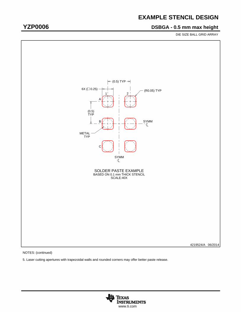
EXAMPLE STENCIL DESIGN
(0.5)TYP
(0.5) TYP
6X ( 0.25) (R ) TYP0.05
METALTYP
4219524/A 06/2014
DSBGA - 0.5 mm max heightYZP0006DIE SIZE BALL GRID ARRAY
NOTES: (continued) 5. Laser cutting apertures with trapezoidal walls and rounded corners may offer better paste release.
SYMM
SYMM
SOLDER PASTE EXAMPLEBASED ON 0.1 mm THICK STENCIL
SCALE:40X
1 2
A
B
C
IMPORTANT NOTICE
Texas Instruments Incorporated (TI) reserves the right to make corrections, enhancements, improvements and other changes to itssemiconductor products and services per JESD46, latest issue, and to discontinue any product or service per JESD48, latest issue. Buyersshould obtain the latest relevant information before placing orders and should verify that such information is current and complete.TI’s published terms of sale for semiconductor products (http://www.ti.com/sc/docs/stdterms.htm) apply to the sale of packaged integratedcircuit products that TI has qualified and released to market. Additional terms may apply to the use or sale of other types of TI products andservices.Reproduction of significant portions of TI information in TI data sheets is permissible only if reproduction is without alteration and isaccompanied by all associated warranties, conditions, limitations, and notices. TI is not responsible or liable for such reproduceddocumentation. Information of third parties may be subject to additional restrictions. Resale of TI products or services with statementsdifferent from or beyond the parameters stated by TI for that product or service voids all express and any implied warranties for theassociated TI product or service and is an unfair and deceptive business practice. TI is not responsible or liable for any such statements.Buyers and others who are developing systems that incorporate TI products (collectively, “Designers”) understand and agree that Designersremain responsible for using their independent analysis, evaluation and judgment in designing their applications and that Designers havefull and exclusive responsibility to assure the safety of Designers' applications and compliance of their applications (and of all TI productsused in or for Designers’ applications) with all applicable regulations, laws and other applicable requirements. Designer represents that, withrespect to their applications, Designer has all the necessary expertise to create and implement safeguards that (1) anticipate dangerousconsequences of failures, (2) monitor failures and their consequences, and (3) lessen the likelihood of failures that might cause harm andtake appropriate actions. Designer agrees that prior to using or distributing any applications that include TI products, Designer willthoroughly test such applications and the functionality of such TI products as used in such applications.TI’s provision of technical, application or other design advice, quality characterization, reliability data or other services or information,including, but not limited to, reference designs and materials relating to evaluation modules, (collectively, “TI Resources”) are intended toassist designers who are developing applications that incorporate TI products; by downloading, accessing or using TI Resources in anyway, Designer (individually or, if Designer is acting on behalf of a company, Designer’s company) agrees to use any particular TI Resourcesolely for this purpose and subject to the terms of this Notice.TI’s provision of TI Resources does not expand or otherwise alter TI’s applicable published warranties or warranty disclaimers for TIproducts, and no additional obligations or liabilities arise from TI providing such TI Resources. TI reserves the right to make corrections,enhancements, improvements and other changes to its TI Resources. TI has not conducted any testing other than that specificallydescribed in the published documentation for a particular TI Resource.Designer is authorized to use, copy and modify any individual TI Resource only in connection with the development of applications thatinclude the TI product(s) identified in such TI Resource. NO OTHER LICENSE, EXPRESS OR IMPLIED, BY ESTOPPEL OR OTHERWISETO ANY OTHER TI INTELLECTUAL PROPERTY RIGHT, AND NO LICENSE TO ANY TECHNOLOGY OR INTELLECTUAL PROPERTYRIGHT OF TI OR ANY THIRD PARTY IS GRANTED HEREIN, including but not limited to any patent right, copyright, mask work right, orother intellectual property right relating to any combination, machine, or process in which TI products or services are used. Informationregarding or referencing third-party products or services does not constitute a license to use such products or services, or a warranty orendorsement thereof. Use of TI Resources may require a license from a third party under the patents or other intellectual property of thethird party, or a license from TI under the patents or other intellectual property of TI.TI RESOURCES ARE PROVIDED “AS IS” AND WITH ALL FAULTS. TI DISCLAIMS ALL OTHER WARRANTIES ORREPRESENTATIONS, EXPRESS OR IMPLIED, REGARDING RESOURCES OR USE THEREOF, INCLUDING BUT NOT LIMITED TOACCURACY OR COMPLETENESS, TITLE, ANY EPIDEMIC FAILURE WARRANTY AND ANY IMPLIED WARRANTIES OFMERCHANTABILITY, FITNESS FOR A PARTICULAR PURPOSE, AND NON-INFRINGEMENT OF ANY THIRD PARTY INTELLECTUALPROPERTY RIGHTS. TI SHALL NOT BE LIABLE FOR AND SHALL NOT DEFEND OR INDEMNIFY DESIGNER AGAINST ANY CLAIM,INCLUDING BUT NOT LIMITED TO ANY INFRINGEMENT CLAIM THAT RELATES TO OR IS BASED ON ANY COMBINATION OFPRODUCTS EVEN IF DESCRIBED IN TI RESOURCES OR OTHERWISE. IN NO EVENT SHALL TI BE LIABLE FOR ANY ACTUAL,DIRECT, SPECIAL, COLLATERAL, INDIRECT, PUNITIVE, INCIDENTAL, CONSEQUENTIAL OR EXEMPLARY DAMAGES INCONNECTION WITH OR ARISING OUT OF TI RESOURCES OR USE THEREOF, AND REGARDLESS OF WHETHER TI HAS BEENADVISED OF THE POSSIBILITY OF SUCH DAMAGES.Unless TI has explicitly designated an individual product as meeting the requirements of a particular industry standard (e.g., ISO/TS 16949and ISO 26262), TI is not responsible for any failure to meet such industry standard requirements.Where TI specifically promotes products as facilitating functional safety or as compliant with industry functional safety standards, suchproducts are intended to help enable customers to design and create their own applications that meet applicable functional safety standardsand requirements. Using products in an application does not by itself establish any safety features in the application. Designers mustensure compliance with safety-related requirements and standards applicable to their applications. Designer may not use any TI products inlife-critical medical equipment unless authorized officers of the parties have executed a special contract specifically governing such use.Life-critical medical equipment is medical equipment where failure of such equipment would cause serious bodily injury or death (e.g., lifesupport, pacemakers, defibrillators, heart pumps, neurostimulators, and implantables). Such equipment includes, without limitation, allmedical devices identified by the U.S. Food and Drug Administration as Class III devices and equivalent classifications outside the U.S.TI may expressly designate certain products as completing a particular qualification (e.g., Q100, Military Grade, or Enhanced Product).Designers agree that it has the necessary expertise to select the product with the appropriate qualification designation for their applicationsand that proper product selection is at Designers’ own risk. Designers are solely responsible for compliance with all legal and regulatoryrequirements in connection with such selection.Designer will fully indemnify TI and its representatives against any damages, costs, losses, and/or liabilities arising out of Designer’s non-compliance with the terms and provisions of this Notice.
Mailing Address: Texas Instruments, Post Office Box 655303, Dallas, Texas 75265Copyright © 2018, Texas Instruments Incorporated
Related Documents