March 2016 DocID027795 Rev 1 1/25 1 AN4688 Application note Sensorless BLDC Motor Control using SPC574K72xx Introduction This document describes the design of a three-phase brushless DC (BLDC) motor control drive using a sensorless algorithm. The design is targeted at automotive applications. This cost-effective solution is based on the STMicroelectronics SPC574K72xx devices. www.st.com

Welcome message from author
This document is posted to help you gain knowledge. Please leave a comment to let me know what you think about it! Share it to your friends and learn new things together.
Transcript
March 2016 DocID027795 Rev 1 1/25
1
AN4688Application note
Sensorless BLDC Motor Control using SPC574K72xx
IntroductionThis document describes the design of a three-phase brushless DC (BLDC) motor control drive using a sensorless algorithm.
The design is targeted at automotive applications. This cost-effective solution is based on the STMicroelectronics SPC574K72xx devices.
www.st.com
Contents AN4688
2/25 DocID027795 Rev 1
Contents
1 BLDC sensorless control . . . . . . . . . . . . . . . . . . . . . . . . . . . . . . . . . . . . . 5
1.1 Principle of BLDC sensorless control . . . . . . . . . . . . . . . . . . . . . . . . . . . . . 5
1.2 BEMF zero-crossing detection . . . . . . . . . . . . . . . . . . . . . . . . . . . . . . . . . . 6
2 System concept . . . . . . . . . . . . . . . . . . . . . . . . . . . . . . . . . . . . . . . . . . . . . 8
3 Hardware and software implementation . . . . . . . . . . . . . . . . . . . . . . . . . 9
3.1 GTM global initialization . . . . . . . . . . . . . . . . . . . . . . . . . . . . . . . . . . . . . . . 9
3.2 SARADCx (with x = 0,2,6) configuration . . . . . . . . . . . . . . . . . . . . . . . . . .11
3.3 TIM1_CHx (with x = 0,1,2) configuration . . . . . . . . . . . . . . . . . . . . . . . . . 13
3.4 AT0M0_CHx (with x = 3,4,5) configuration . . . . . . . . . . . . . . . . . . . . . . . . 14
3.5 TIM0_CHx (with x = 3,4,5) configuration . . . . . . . . . . . . . . . . . . . . . . . . . 15
3.6 SPE1 configuration . . . . . . . . . . . . . . . . . . . . . . . . . . . . . . . . . . . . . . . . . . 16
3.7 TOM0_CHy (with y = 14,15) configuration . . . . . . . . . . . . . . . . . . . . . . . . 17
3.8 TOM1_CHx (with x = 0,1,2,3,4,5,6) configuration . . . . . . . . . . . . . . . . . . 18
3.9 TOM1_CH2 and SPE1 output update delay . . . . . . . . . . . . . . . . . . . . . . 20
3.10 Speed evaluation and control . . . . . . . . . . . . . . . . . . . . . . . . . . . . . . . . . . 20
4 Conclusion . . . . . . . . . . . . . . . . . . . . . . . . . . . . . . . . . . . . . . . . . . . . . . . . 22
Appendix A Further information . . . . . . . . . . . . . . . . . . . . . . . . . . . . . . . . . . . . . . 23
A.1 Reference documents . . . . . . . . . . . . . . . . . . . . . . . . . . . . . . . . . . . . . . . . 23
A.2 Terms and abbreviations . . . . . . . . . . . . . . . . . . . . . . . . . . . . . . . . . . . . . . 23
Revision history . . . . . . . . . . . . . . . . . . . . . . . . . . . . . . . . . . . . . . . . . . . . . . . . . . . . 24
DocID027795 Rev 1 3/25
AN4688 List of tables
3
List of tables
Table 1. GTM clock sources configuration . . . . . . . . . . . . . . . . . . . . . . . . . . . . . . . . . . . . . . . . . . . . 10Table 2. SPE1_OUT_PATx (with x = 0,1,3,4,5) register configuration . . . . . . . . . . . . . . . . . . . . . . . 16Table 3. SPE1_PAT register configuration . . . . . . . . . . . . . . . . . . . . . . . . . . . . . . . . . . . . . . . . . . . . 17Table 4. TOM1_CHx (with x = 0,1,2,3,4,5,6) configuration. . . . . . . . . . . . . . . . . . . . . . . . . . . . . . . . 19Table 5. Acronyms . . . . . . . . . . . . . . . . . . . . . . . . . . . . . . . . . . . . . . . . . . . . . . . . . . . . . . . . . . . . . . 23Table 6. Document revision history . . . . . . . . . . . . . . . . . . . . . . . . . . . . . . . . . . . . . . . . . . . . . . . . . 24
List of figures AN4688
4/25 DocID027795 Rev 1
List of figures
Figure 1. Three phase voltage signals and BEMF. . . . . . . . . . . . . . . . . . . . . . . . . . . . . . . . . . . . . . . . 6Figure 2. BEMF sensing scheme. . . . . . . . . . . . . . . . . . . . . . . . . . . . . . . . . . . . . . . . . . . . . . . . . . . . . 7Figure 3. Application block diagram. . . . . . . . . . . . . . . . . . . . . . . . . . . . . . . . . . . . . . . . . . . . . . . . . . . 9Figure 4. BEMF zero-cross detection signals . . . . . . . . . . . . . . . . . . . . . . . . . . . . . . . . . . . . . . . . . . 13Figure 5. System control states . . . . . . . . . . . . . . . . . . . . . . . . . . . . . . . . . . . . . . . . . . . . . . . . . . . . . 17
DocID027795 Rev 1 5/25
AN4688 BLDC sensorless control
23
1 BLDC sensorless control
1.1 Principle of BLDC sensorless controlThe BLDC motor is a rotating electric machine with a classic three-phase stator and with a rotor with surface-mounted permanent magnets.
The commutation is performed electronically at a certain rotor position and the displacement of the magnets on the rotor creates a trapezoidal Back Electro Magnetic Force (BEMF) shape.
The motor can have more than one pole pair per phase. The pole pairs per phase define the ratio between the electrical revolution and the mechanical revolution.
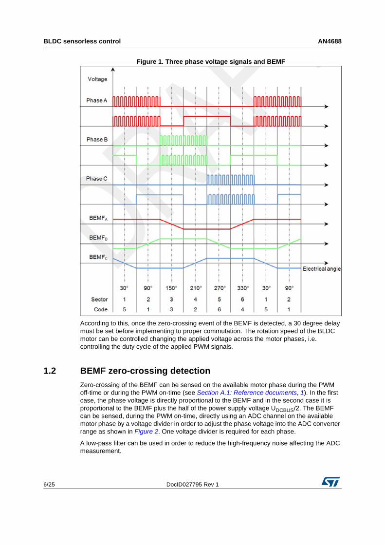
The rotor position must be known in order to align the applied voltage with the BEMF and to achieve the best efficiency. For three-phase BLDC motors, six-step commutation with 120 degree conduction time allows the current to flow in only two phases at any one time and this leaves the third phase available for sensing BEMF.
Since the BEMF is directly related to the rotor position, sensing the BEMF enables the controller to drive the motor, in fact each zero-crossing event of the BEMF precedes a commutation event by 30 electrical degrees as shown in Figure 1.
BLDC sensorless control AN4688
6/25 DocID027795 Rev 1
Figure 1. Three phase voltage signals and BEMF
According to this, once the zero-crossing event of the BEMF is detected, a 30 degree delay must be set before implementing to proper commutation. The rotation speed of the BLDC motor can be controlled changing the applied voltage across the motor phases, i.e. controlling the duty cycle of the applied PWM signals.
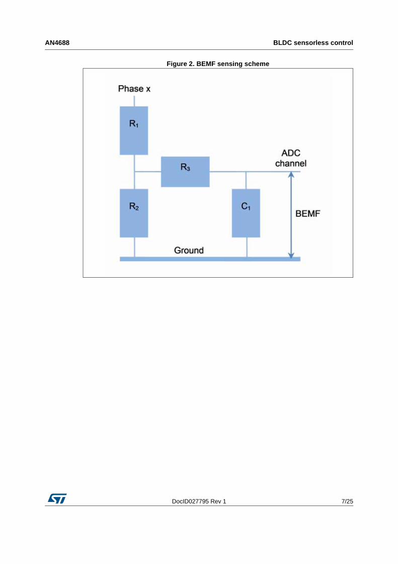
1.2 BEMF zero-crossing detectionZero-crossing of the BEMF can be sensed on the available motor phase during the PWM off-time or during the PWM on-time (see Section A.1: Reference documents, 1). In the first case, the phase voltage is directly proportional to the BEMF and in the second case it is proportional to the BEMF plus the half of the power supply voltage UDCBUS/2. The BEMF can be sensed, during the PWM on-time, directly using an ADC channel on the available motor phase by a voltage divider in order to adjust the phase voltage into the ADC converter range as shown in Figure 2. One voltage divider is required for each phase.
A low-pass filter can be used in order to reduce the high-frequency noise affecting the ADC measurement.
DocID027795 Rev 1 7/25
AN4688 BLDC sensorless control
23
Figure 2. BEMF sensing scheme
System concept AN4688
8/25 DocID027795 Rev 1
2 System concept
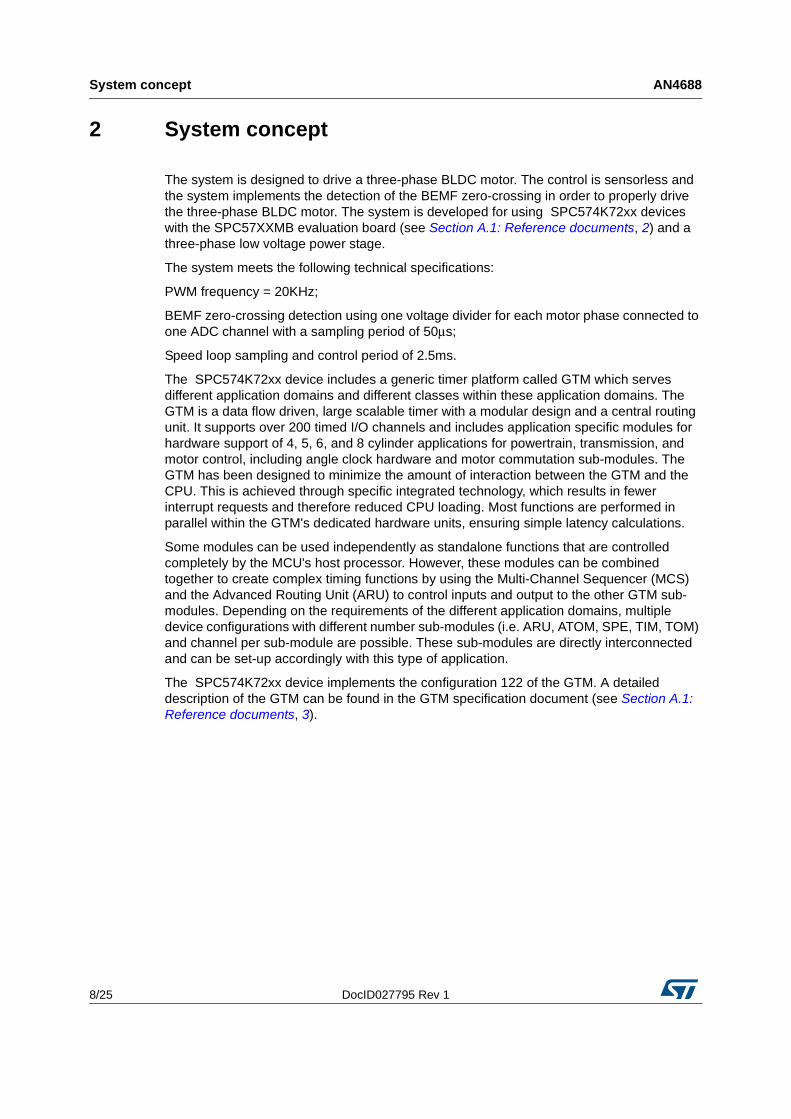
The system is designed to drive a three-phase BLDC motor. The control is sensorless and the system implements the detection of the BEMF zero-crossing in order to properly drive the three-phase BLDC motor. The system is developed for using SPC574K72xx devices with the SPC57XXMB evaluation board (see Section A.1: Reference documents, 2) and a three-phase low voltage power stage.
The system meets the following technical specifications:
PWM frequency = 20KHz;
BEMF zero-crossing detection using one voltage divider for each motor phase connected to one ADC channel with a sampling period of 50μs;
Speed loop sampling and control period of 2.5ms.
The SPC574K72xx device includes a generic timer platform called GTM which serves different application domains and different classes within these application domains. The GTM is a data flow driven, large scalable timer with a modular design and a central routing unit. It supports over 200 timed I/O channels and includes application specific modules for hardware support of 4, 5, 6, and 8 cylinder applications for powertrain, transmission, and motor control, including angle clock hardware and motor commutation sub-modules. The GTM has been designed to minimize the amount of interaction between the GTM and the CPU. This is achieved through specific integrated technology, which results in fewer interrupt requests and therefore reduced CPU loading. Most functions are performed in parallel within the GTM's dedicated hardware units, ensuring simple latency calculations.
Some modules can be used independently as standalone functions that are controlled completely by the MCU's host processor. However, these modules can be combined together to create complex timing functions by using the Multi-Channel Sequencer (MCS) and the Advanced Routing Unit (ARU) to control inputs and output to the other GTM sub-modules. Depending on the requirements of the different application domains, multiple device configurations with different number sub-modules (i.e. ARU, ATOM, SPE, TIM, TOM) and channel per sub-module are possible. These sub-modules are directly interconnected and can be set-up accordingly with this type of application.
The SPC574K72xx device implements the configuration 122 of the GTM. A detailed description of the GTM can be found in the GTM specification document (see Section A.1: Reference documents, 3).
DocID027795 Rev 1 9/25
AN4688 Hardware and software implementation
23
3 Hardware and software implementation
This section describes the hardware and software implementation of the system. The Figure 3 shows the application block diagram.
Figure 3. Application block diagram
3.1 GTM global initializationTo run the GTM-122 on the SPC574K72xx device at its maximum speed, it is recommended that:
• FMPLL1 is configured to run at 200MHz and PBRIDGEA_CLK set to FMPLL1 divided by 4,
• FMPLL0 running at 160 MHz and divided by 2 for the source of the PER_CLK. This 80 MHz clock is used by the GTM CMU sub-module to derive the GTM's local clock signals for its sub-modules and the GTM's external clock signals.
Hardware and software implementation AN4688
10/25 DocID027795 Rev 1
The GTM's timing clock source is SYS_CLK, which is the PER_CLK signal at the chip level. The SPC574K72xx device's reference manual (see Section A.1: Reference documents, 4) describes the maximum frequencies for the PBRIDGEA_CLK and PER_CLK clocks inside their respective System clock frequency limitations section in the Clocking chapter.
Assuming FMPLLs and all other clock sources are properly configured, the first step to enable the GTM is to configure the Slow Crossbar and peripheral clocks to the Mode Entry (MC_ME) module's Run Peripheral Configuration 0 register (ME_RUN_PC0) (refer to the SPC574K72xx device's reference manual (see Section A.1: Reference documents, 4) for all needed details about MC_ME configuration).
The clocks to the GTM do not become active until the run mode is updated in the MC_ME module. Afterwards the GTM can be enabled by clearing the Module Disable (MDIS) in the GTM Module Configuration Register (GTMINT.GTMMCR_MDIS = 0DEC). This MDIS bit must be cleared to enable writes to the GTM registers for configuration before operation. After the clearing of MDIS bit, AEI protected write responses can be unmasked, the AEI bridge mode can be selected as asynchronous and the buffer depth of AEI bridge is defined (GTM_BRIDGE_MODE = 0x04000001HEX).
Finally, there are other four steps to enable the GTM internal clocks using the CMU sub-module:
• set the global clock divider ratio, i.e. to define the global clock CMU_GCLK_EN as a fraction of the PER_CLK, writing the numerator and denominator values of the relevant divider. In our implementation CMU_GCLK_NUM = 0xFFFFFFHEX and CMU_GCLK_DEN = 0xFFFFFFHEX in order to have CMU_GCLK_EN = PER_CLK = 80MHz.
• select the fixed-frequency clock divider FXCLK. The CMU_FXCLK0 clock is used by the TOM sub-module for PWM generation. In our implementation CMU_FXCLK_CTRL = 0x0HEX in order to select CMU_GCLK_EN as source, i.e. FXCLK = CMU_GCLK_EN = 80MHz.
• select the source and divider for each CLKn (with n = 0,1,2,3,4,5,6,7) signal. In our implementation CMU_CLK0_CTRL = 0x000001HEX and CMU_CLK1_CTRL = 0x00004FHEX. CMU_CLK0 = 40MHz is used for TIM1_CHx (with x = 0,1,2) and CMU_CLK1 = 1MHz is used for TIM0_CHx (with x = 3,4,5).
• enable the configured clocks. In our implementation CMU_CLK_EN = 0x0080000A in order to enable FXCLK, CMU_CLK0 and CMU_CLK1. The configuration is summarized in the Table 1.
For more details see the GTM specification document (see Section A.1: Reference documents, 3).
Table 1. GTM clock sources configuration
Clock sourceFrequency
[MHz]Derived from
Used by GTM sub-module
FMPLL0 160 At the chip level ---
FMPLL1 200 At the chip level ---
PBRIDGEA_CLK
50 FMPLL1 / 4 ---
PER_CLK 80 FMPLL0 / 2GTM interface and all sub-
modules except the following
DocID027795 Rev 1 11/25
AN4688 Hardware and software implementation
23
3.2 SARADCx (with x = 0,2,6) configurationThe SARADC digital interface block controls the on-chip SARADC analog block and holds control and status registers accessible for the application. It provides accurate and fast conversion data for a wide range of applications. Each SARADC analog block has its corresponding digital interface implemented at the SoC level.
The SARADC digital interface contains advanced features for normal or injected conversion modes of operation. The conversion can be triggered by software or hardware.
The mask registers present within the digital interface can be properly programmed to configure which channel has to be converted. External channel selection is provided through external decode signals and are available as alternate functions on GPIO. Each set of eight external channels can be mapped to any internal analog channel by static programming by software in specific registers.
Four conversion timing registers exist that allow configuration of different pre-charging and sampling durations, and it is possible to select one of the conversion timing registers for each channel. For each channel, it is possible to choose the voltage reference through software. Configurable number of analog watchdogs allows continuous hardware monitoring of analog input channels with trigger outputs on watchdog threshold crossover events. The digital interface also provides for interrupt/DMA support for various conditions related to end of channel conversions.
For more details see the SPC574K72xx device's reference manual (see Section A.1: Reference documents, 4).
BEMF voltage is measured using one divider for each inverter leg. Each phase voltage is routed to a SARADCx (with x = 0,2,6) channel follows:
• Phase A BEMF SARADC0_CH4 on PAD PD[11] (SIUL2_MSCR59_APC = 1DEC);
• Phase B BEMF SARADC2_CH16 on PAD PG[8] (SIUL2_MSCR104_APC = 1DEC);
• Phase C BEMF SARADC6_CH48 on PAD PI[9] (SIUL2_MSCR137_APC = 1DEC);
The FMPLL0 frequency is set to 160MHz and the SARADCx frequency is set to 10MHz (MC_CGM_AC0_DC2 = 0x800F0000HEX with DIV = 15DEC).
CMU_GCLK_EN
80PER_CLK(CMU_GCLK_NUM = CMU_GCLK_DEN = 0xFFFFFFHEX)
CMU
CMU_FXCLK0
80CMU_GCLK_EN
(CMU_FXCLK_CTRL = 0x0HEX)TOM1_CHx (with x =
0,1,2,3,4,5,6)
CMU_FXCLK2
0,3125CMU_GCLK_EN / 2^8
(CMU_FXCLK_CTRL = 0x0HEX)TOM1_CH2
CMU_CLK0 40CMU_GCLK_EN / 2
(CMU_CLK0_CTRL = 0x000001HEX)TIM1_CHx (with x = 0,1,2)
CMU_CLK1 1CMU_GCLK_EN / 80
(CMU_CLK1_CTRL = 0x00004FHEX)TIM0_CHx (with x = 3,4,5)
Table 1. GTM clock sources configuration (continued)
Clock sourceFrequency
[MHz]Derived from
Used by GTM sub-module
Hardware and software implementation AN4688
12/25 DocID027795 Rev 1
Note: SARADCx maximum frequency is 14,6MHz, anyway the maximum allowed value for this application is 10MHz because SARADCx frequency must be synchronous with TIM1_CHx (with x = 0,1,2) in order to avoid delay due to the resynchronization in the occurrence of SARADCx watchdog 3 pulses.
The conversion timing is defined by the conversion timing register, for example SARADCx_CTR0. This register contains PRECHG and INPSAMP fields to define the required duration for pre-charging and sampling phases. The selection of this register for each SARADCx channel is done by the CTSEL bit field of corresponding channel data register (CTR0 is selected by default). The total conversion duration for 12-bit conversion (not including external multiplexing) is given by the following formula:
tconv = tprechg + tsample + teval = (PRECHG + INPSAMP + 25) / fSARADCx
Considering that PRECHG = 3DEC and INPSAMP = 8DEC in order to have a pre-charging time and a sampling time greater than the minimum required respectively equal to 270ns and 750ns (SARADCx_CTR0 = 0x00000308HEX, SARADC_x_ICDRy_PCE = 1DEC with x = 0,2,6 and y = 4,16,48), the total conversion duration for 12-bit conversion is tconv = 3,600μs.
Each SARADCx (with x = 0,2,6) is configured in order to start an injected conversion (SARADCx_MCR_JTRGEN = 1DEC) on the relevant channel (SARADC0_ICJCMR0 = 0x00000010HEX, SARADC2_ICJCMR0 = 0x00010000HEX, SARADC6_ICJCMR1 = 0x00010000HEX) with overwrite enabled (SARADCx_MCR_OWREN = 1DEC) according to the occurrence of the falling edge (SARADCx_MCR_JEDGESEL = 0DEC) of TOM0_CH14 (SIUL2_MSCR608 = 0x13HEX, SIUL2_MSCR610 = 0x13HEX, SIUL2_MSCR614 = 0x13HEX).
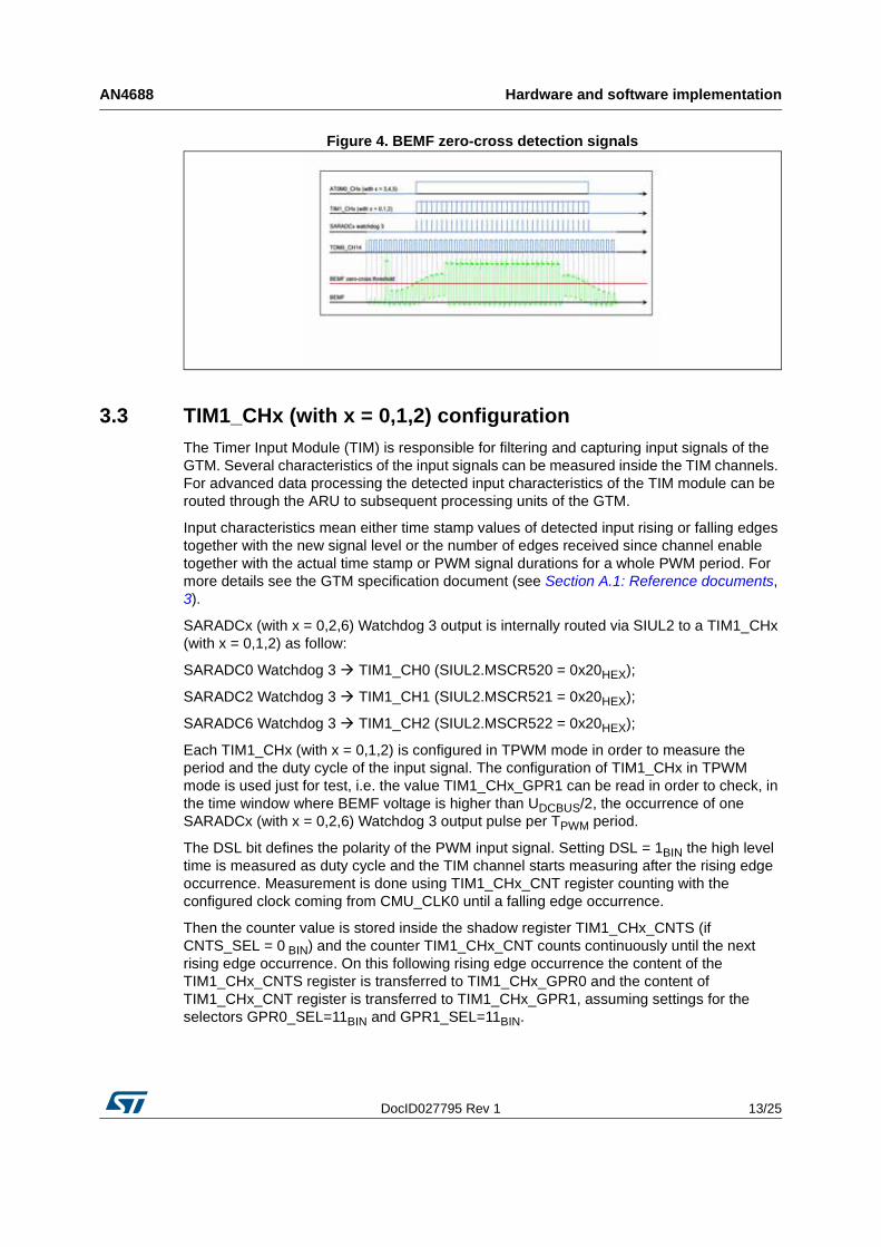
TOM0_CH14 is configured to generate a PWM signal with period equals to TPWM (period of PWM outputs) and with a 50% duty cycle. TOM0_CH14 is started synchronously with TOM0_CH15 (for more details see Section 3.7). According to this, BEMF voltage is measured one time per TPWM period starting on the middle of the period, i.e. BEMF voltage is measured during the PWM on-time.
BEMF voltage zero-cross event occurs when BEMF voltage crosses the UDCBUS/2 and it is detected for each SARADCx channel using the watchdog 3 (SARADC0_ICWSELR0 = 0x00030000HEX, SARADC2_ICWSELR2 = 0x00000003HEX, SARADC6_ICWSELR6 = 0x00000003HEX) with low threshold set at default value (SARADCx_WTHRHLR3_THLH = 0DEC) and high threshold set to VADCREF/2 (SARADCx_WTHRHLR3_THRH = 2047DEC). According to this configuration, when BEMF voltage crosses the UDCBUS/2, for each motor phase the relevant SARADCx watchdog 3 generates a pulse with an on-time equals to 1 PER_CLK cycle (see Figure 4).
Finally each SARADCx (with x = 0,2,6) is powered up (SARADCx_MCR_PWDN = 0DEC).
DocID027795 Rev 1 13/25
AN4688 Hardware and software implementation
23
Figure 4. BEMF zero-cross detection signals
3.3 TIM1_CHx (with x = 0,1,2) configurationThe Timer Input Module (TIM) is responsible for filtering and capturing input signals of the GTM. Several characteristics of the input signals can be measured inside the TIM channels. For advanced data processing the detected input characteristics of the TIM module can be routed through the ARU to subsequent processing units of the GTM.
Input characteristics mean either time stamp values of detected input rising or falling edges together with the new signal level or the number of edges received since channel enable together with the actual time stamp or PWM signal durations for a whole PWM period. For more details see the GTM specification document (see Section A.1: Reference documents, 3).
SARADCx (with x = 0,2,6) Watchdog 3 output is internally routed via SIUL2 to a TIM1_CHx (with x = 0,1,2) as follow:
SARADC0 Watchdog 3 TIM1_CH0 (SIUL2.MSCR520 = 0x20HEX);
SARADC2 Watchdog 3 TIM1_CH1 (SIUL2.MSCR521 = 0x20HEX);
SARADC6 Watchdog 3 TIM1_CH2 (SIUL2.MSCR522 = 0x20HEX);
Each TIM1_CHx (with x = 0,1,2) is configured in TPWM mode in order to measure the period and the duty cycle of the input signal. The configuration of TIM1_CHx in TPWM mode is used just for test, i.e. the value TIM1_CHx_GPR1 can be read in order to check, in the time window where BEMF voltage is higher than UDCBUS/2, the occurrence of one SARADCx (with x = 0,2,6) Watchdog 3 output pulse per TPWM period.
The DSL bit defines the polarity of the PWM input signal. Setting DSL = 1BIN the high level time is measured as duty cycle and the TIM channel starts measuring after the rising edge occurrence. Measurement is done using TIM1_CHx_CNT register counting with the configured clock coming from CMU_CLK0 until a falling edge occurrence.
Then the counter value is stored inside the shadow register TIM1_CHx_CNTS (if CNTS_SEL = 0 BIN) and the counter TIM1_CHx_CNT counts continuously until the next rising edge occurrence. On this following rising edge occurrence the content of the TIM1_CHx_CNTS register is transferred to TIM1_CHx_GPR0 and the content of TIM1_CHx_CNT register is transferred to TIM1_CHx_GPR1, assuming settings for the selectors GPR0_SEL=11BIN and GPR1_SEL=11BIN.
Hardware and software implementation AN4688
14/25 DocID027795 Rev 1
As result TIM1_CHx_GPR0 contains the duty cycle length and TIM1_CHx_GPR1 contains the period. The bits 1 to 7 of the TIM0_CHx_ECNT can be used to check data consistency of the registers TIM0_CHx_GPR0 and TIM0_CHx_GPR1.
Moreover, TIM1_CHx_FLT (FLT_EN = 1, FLT_CNT_FRQ = CMU_CLK0) is used to filter the input signal. FLT_MODE_RE is set to immediate edge propagation mode with FLT_RE equals to 0 and FLT_MODE_FE is set to individual de-glitch mode with FLT_FE equals to NTIM_CLK_CYCLE – 2 where NTIM_CLK_CYCLE = TPWM / TIM_CLK_SEL with TIM_CLK_SEL = CMU_CLK0.
According to this, TIM1_CHx output (F_OUT signal), when BEMF voltage crosses the UDCBUS/2, i.e. the relevant SARADCx watchdog 3 generates a pulse, is a PWM signal with TPWM period and with duty cycle equals to (NTIM_CLK_CYCLE – 1) / NTIM_CLK_CYCLE (see Figure 4).
3.4 AT0M0_CHx (with x = 3,4,5) configurationThe ARU-connected Timer Output Module (ATOM) is able to generate complex output signals without CPU interaction due to its connectivity to the ARU. Typically, output signal characteristics are provided over the ARU connection through sub-modules connected to ARU like e.g. the TIM. Each ATOM sub-module contains eight output channels which can operate independently from each other in several configurable operation modes. For more details see the GTM specification document (see Section A.1: Reference documents, 3).
TIM1_CHx (with x = 0,1,3) output (F_OUT signal) is internally routed via ARU (TIM1_CHx_ARU_EN =1BIN) to a ATOM0_CHx (with x = 3,4,5) as follow (ATOM0_CHx_CTRL = 0x000808HEX):
• TIM1_CH0 F_OUT ATOM0_CH3 (ATOM0_CH3_RDADDR = 0x000009);
• TIM1_CH1 F_OUT ATOM0_CH4 (ATOM0_CH4_RDADDR = 0x00000A);
• TIM1_CH2 F_OUT ATOM0_CH5 (ATOM0_CH5_RDADDR = 0x00000B);
Each ATOM0_CHx (with x = 3,4,5) is configured in ATOM Signal Output Mode Immediate (SOMI). In SOMI mode, the ATOM channel generates output signals on the ATOM0_CHx_OUT output port immediate after update of the bit ACBI(0) of register ATOM0_CHx_STAT or ACB(0) bit of register ATOM0_CHx_CTRL.
Incoming ARU data (53 bit width signal ARU_CHx_IN) is split into three parts by the ACI and communicated to the ATOM channel registers. In SOMI mode incoming ARU data, i.e. ARU_CHx_IN, is split in a way that the lower 24 bits of the ARU data (23 down to 0) are stored in the SR0 register, the upper bits (47 down to 24) are stored in the SR1 register and the bits 52 down to 48 (CTRL_BITS) are stored in the ACBI bit field of the register ATOM0_CHx_STAT.
Considering that TIM1_CHx (with x = 0,1,3) output (F_OUT signal) is routed as ARU_OUT(48) signal, the bit ACBI(0) and the ATOM0_CHx_OUT output are set according to the level of TIM1_CHx (with x = 0,1,3) output (F_OUT signal).
Moreover, the ATOM0_CHx_OUT output is not able to detect a single clock cycle low level of the TIM1_CHx output (F_OUT signal), so ATOM0_CHx_OUT output port level is always high when BEMF voltage is higher than UDCBUS/2 and it is always low when BEMF voltage is lower than UDCBUS/2 (see Figure 4). This type of signal can be used in the same way of an Hall sensor output signal.
Finally each ATOM0_CHx (with x = 3,4,5) is enabled (ATOM0_AGC_GLB_CTRL = 0x0A800000HEX, ATOM0_AGC_ENDIS_CTRL = 0x0A80HEX,
DocID027795 Rev 1 15/25
AN4688 Hardware and software implementation
23
ATOM0_AGC_OUTEN_CTRL = 0x0A80HEX) and a trigger request is set (ATOM0_AGC_GLB_CTRL |= 0x00000001HEX).
3.5 TIM0_CHx (with x = 3,4,5) configurationThe Timer Input Module (TIM) is responsible for filtering and capturing input signals of the GTM. Several characteristics of the input signals can be measured inside the TIM channels. For advanced data processing the detected input characteristics of the TIM module can be routed through the ARU to subsequent processing units of the GTM.
Input characteristics mean either time stamp values of detected input rising or falling edges together with the new signal level or the number of edges received since channel enable together with the actual time stamp or PWM signal durations for a whole PWM period. For more details see the GTM specification document (see Section A.1: Reference documents, 3).
ATOM0_CHx (with x = 3,4,5) output is internally routed via GTM signal multiplex to a TIM0_CHx (with x = 3,4,5) as follow (TIM0_IN_SRC = 0x00222000HEX, TIM0_AUX_IN_SRC = 0x00000038HEX):
• AT0M0_CH3 TIM0_CH3;
• AT0M0_CH4 TIM0_CH4;
• AT0M0_CH5 TIM0_CH5;
Each TIM0_CHx (with x = 3,4,5) is configured in TPWM mode in order to measure the period and the duty cycle of the input signal.
The DSL bit defines the polarity of the PWM input signal. Setting DSL = 1BIN the high level time is measured as duty cycle and the TIM channel starts measuring after the rising edge occurrence. Measurement is done using TIM0_CHx_CNT register counting with the configured clock coming from CMU_CLK1 until a falling edge occurrence. Then the counter value is stored inside the shadow register TIM0_CHx_CNTS (if CNTS_SEL = 0 BIN) and the counter TIM0_CHx_CNT counts continuously until the next rising edge occurrence. On this following rising edge occurrence the content of the TIM0_CHx_CNTS register is transferred to TIM0_CHx_GPR0 and the content of TIM0_CHx_CNT register is transferred to TIM0_CHx_GPR1, assuming settings for the selectors GPR0_SEL=11BIN and GPR1_SEL=11BIN.
As result TIM0_CHx_GPR0 contains the duty cycle length and TIM0_CHx_GPR1 contains the period. The bits 1 to 7 of the TIM0_CHx_ECNT may be used to check data consistency of the registers TIM0_CHx_GPR0 and TIM0_CHx_GPR1.
Moreover, TIM0_CHx_FLT (FLT_EN = 1, FLT_CNT_FRQ = CMU_CLK1) is used to filter the input signal. FLT_MODE_RE and FLT_MODE_FE are set to immediate edge propagation mode with FLT_RE = FLT_FE = N * TPWM * CMU_CLK1. According to this, TIM0_CHx ignores the input level until the acceptance time N * TPWM is expired, i.e. the following N – 1 BEMF measurements after the occurrence of a BEMF zero-cross event are ignored. This filtering mode can be useful at low motor speed where the slope of BEMF voltage is too low to have a single zero-cross event and also to avoid the detection of a wrong BACKEMF zero-crossing due to the high voltage spike occurring on each change of SPE1 output pattern.
The period of the input signal is used to calculate the motor speed and to set the correct update delay for SPE1 output according to the BEMF zero-cross event time.
Hardware and software implementation AN4688
16/25 DocID027795 Rev 1
TIM1_CHx (with x = 0,1,2) are used to manage the signals coming from SARADCx (with x = 0,2,6) Watchdog 3 while TIM0_CHx (with x = 3,4,5) are used to manage the signals coming from ATOM0_CHx (with x = 3,4,5), As result, the configurations of TIM1_CHx_FLT (with x = 0,1,2) and TIM0_CHx_FLT (with x = 3,4,5) are different.
3.6 SPE1 configurationMoreover GTM offers a dedicated sub-module which can be used in combination with other sub-modules to drive a BLDC motor. This sub-module is the Sensor Pattern Evaluator (SPE).
The SPE sub-module is able to evaluate three input signals coming, for example, from three HALL sensors, through three TIM input channels routed to the SPE sub-module. According to the detected sensor pattern, the SPE sub-module is able to set the proper PWM output using the TOM channels in order to support the drive of BLDC motor.
The SPE1 module is used to evaluate three TIM0_CHx inputs (with x = 3,4,5) in order to automatically manage the six TOM1_CHx outputs (with x = 0,1,3,4,5,6) plus the TOM1_CH2 to support the sensorless drive of a BLDC motor based on BACKEMF zero-cross detection. For more details see the GTM specification document (see Section A.1: Reference documents, 3).
SPE1_OUT_PATx (with x = 0,1,3,4,5,6) and SPE1_PAT are configured as shown in Table 1 and Table 2. Finally SPE1_CTRL_STAT is configured (SIE0 = 1BIN, SIE1 = 1BIN, SIE2 = 1BIN, TIM_SEL = 0BIN and TRIG_SEL = 11BIN).
Table 2. SPE1_OUT_PATx (with x = 0,1,3,4,5) register configuration
SPE1_OUT_PATx (with x = 0,1,3,4,5) register
xSPE_OUT_PA
T[13:12]SPE_OUT_PA
T[11:10]SPE_OUT_P
AT[9:8]SPE_OUT_P
AT[7:7]SPE_OUT_P
AT[3:2]SPE_OUT_P
AT[1:0]
0 0 0 1 0TOM_CH1_S
OURTOM_CH0_S
OUR
1 1 0 0 0TOM_CH1_S
OURTOM_CH0_S
OUR
2 1 0TOM_CH1_S
OURTOM_CH0_S
OUR0 0
3 0 0TOM_CH1_S
OURTOM_CH0_S
OUR1 0
4TOM_CH1_SO
URTOM_CH0_SO
UR0 0 1 0
5TOM_CH1_SO
URTOM_CH0_SO
UR1 0 0 0
DocID027795 Rev 1 17/25
AN4688 Hardware and software implementation
23
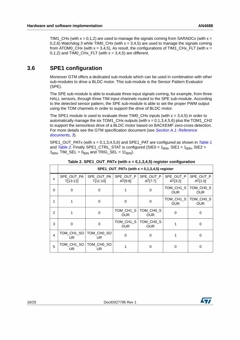
SPE1 is not enabled until the BEMF voltage is high enough to be properly detected.
According to this, the BLDC motor starts in open loop and the SPE output pattern is directly controlled setting the SPE1_OUT_CTRL register and the PWM duty cycle according to a linear open-loop starting ramp.
The open-loop phase is a short state at a very low speed where the BEMF is too small, so when the detection of the BEMF zero-crossing events is stable, the SPE1 is enabled by setting the EN bit-field in the SPE1_CTRL_STAT register and the motor speed is controlled using a PI regulator.
As result the system goes through the states alignment, open-loop and closed-loop. Figure 5 shows the transitions between the states.
Figure 5. System control states
3.7 TOM0_CHy (with y = 14,15) configurationThe Timer Output Module (TOM) offers 16 independent channels to generate simple PWM signals at each output pin TOM[i]_CH[x]_OUT (i = 0,1,2; x = 0,1,2,.,14,15). For more details see the GTM specification document (see Section A.1: Reference documents, 3).
Table 3. SPE1_PAT register configuration
SPE1_PAT
IP4_P
AT
IP5_V
AL
IP4_P
AT
IP4_V
AL
IP3_P
AT
IP3_V
AL
IP2_P
AT
IP2_V
AL
IP1_P
AT
IP1_V
AL
IP0_P
AT
IP0_V
AL
Code 5 1 1 1 3 1 2 1 6 1 4 1
Hardware and software implementation AN4688
18/25 DocID027795 Rev 1
TOM0_CH14 and TOM0_CH15 are configured:
• to use CMU_FXCLK0 clock = PER_CLK = 80MHz (default value for CLK_SRC_SR bit-field in TOM0_CHy_CTRL register);
• to generate an edge-aligned PWM signal with period equals to TPWM = 50μs (TOM0_CHy_SR0 = TPWM, TOM0_CHy_CM0 = TPWM) and with a 50% duty cycle (TOM0_CHy_SR1 = TPWM/2, TOM0_CHy_CM1 = TPWM/2) starting with high level signal (TOM0_CHy_CTRL_SL = 1DEC). The reset of TOM0_CHy_CN0 counter register is done on matching comparison of TOM0_CHy_CM0 (TOM0_CHy_CTRL_TRIGOUT = 1DEC, TOM0_CHy_CTRL_RST_CCU0 = 0DEC).
After the configuration each TOM0_CHy (with y = 14,15) is enabled (TOM0_TGC1_GLB_CTRL = 0x00000000HEX, TOM0_ TGC1_ENDIS_CTRL = 0x0000A000HEX, TOM0_ TGC1_OUTEN_CTRL = 0x0000A000HEX) and a trigger request is set (TOM0_TGC1_GLB_CTRL |= 0x00000001HEX) in order to synchronously start the TOM0_CH14 and TOM0_CH15.
TOM0_CH14 is used to start SARADCx injected conversion and TOM0_CH15 is used to reset TOM1_CHx (with x = 0,1) counter on matching comparison of TOM0_CHy_CM0 in order to have center-aligned PWM outputs.
3.8 TOM1_CHx (with x = 0,1,2,3,4,5,6) configurationThe Timer Output Module (TOM) offers 16 independent channels to generate simple PWM signals at each output pin TOM[i]_CH[x]_OUT (i = 0,1,2; x = 0,1,2,..,14,15). For more details see the GTM specification document (see Section A.1: Reference documents, 3).
The TOM1 sub-module offers in combination with the SPE1 sub-module the BLDC support. To drive a BLDC motor, TOM1_CHx (with x = 0,1,3,4,5,6) can be used. TOM1_CHx (with x = 0,1,2,3,4,5,6) are externally connected to the power stage as follow:
• TOM1_CH0 PWMA_H on PAD PC[2] (SIUL2.MSCR_34.R = 0x22080009HEX)
• TOM1_CH1 PWMA_L on PAD PC[0] (SIUL2.MSCR_32.R = 0x22080009HEX)
• TOM1_CH3 PWMB_H on PAD PA[2] (SIUL2.MSCR_2.R = 0x22080008HEX)
• TOM1_CH4 PWMB_L on PAD PA[1] (SIUL2.MSCR_1.R = 0x22080008HEX)
• TOM1_CH5 PWMC_H on PAD PA[12] (SIUL2.MSCR_12.R = 0x22080008HEX)
• TOM1_CH6 PWMC_L on PAD PA[13] (SIUL2.MSCR_13.R = 0x22080008HEX)
The BLDC support is configured by setting the SPEM bit inside the TOM1_CHx_CTRL register. When this bit is set the TOM channel output is controlled through the SPE_OUT signal coming from the SPE1 sub-module.
The SPE1 sub-module can set the output of each TOM1_CHx to the value 0 or 1 or can use the internal signal TOM1_CH0_SOUR or TOM1_CH1_SOUR coming from the TOM1_CH0 and TOM1_CH1 respectively.
According to this TOM1_CH0 and TOM1_CH1 are configured to generate a couple of complementary PWM signals (SL = 0 for TOM1_CH0 and SL = 1 for TOM1_CH1) with fixed PWM period TPWM = 50μs = 4000TOM1_CHx_CLK_CYCLE, controllable duty cycle and dead-time insertion (fixed according to the characteristics of the used power stage). Such configuration is done by setting the right values for registers SR0/CM0 and SR1/CM1.
In order to have center-aligned PWMs, the reset of the relevant counter register CN0 is done on trigger signal coming from TOM0_CH15 for TOM1_CH0 and from TOM1_CH0
DocID027795 Rev 1 19/25
AN4688 Hardware and software implementation
23
(generated synchronous with one coming from TOM0_CH15) for TOM1_CH1. The clock source is for both CMU_FXCLK0.
The duty cycle is changed updating the relevant shadow registers as describe below where PWMDUTYCYCLE can assume the value from 0 TOM1_CHx_CLK_CYCLE to 3999
TOM1_CHx_CLK_CYCLE:
• TOM1_CH0_SR1 = 2000 - PWMDUTYCYCLE / 2;
• TOM1_CH0_SR0 = 2000 + PWMDUTYCYCLE / 2;
• TOM1_CH1_SR1 = 2000 - PWMDUTYCYCLE / 2 - PWMDEADTIME;
• TOM1_CH1_SR0 = 2000 + PWMDUTYCYCLE / 2 + PWMDEADTIME.
The TOM1_CHx_CM0/CM1 registers are automatically updated on the next reset of the relevant CN0 register on trigger signal coming from TOM0_CH15.
The TOM1_CH2 can be used together with the SPE1 sub-module to trigger a delayed update of the SPE_OUT_CTRL register after new input pattern detected by SPE1 (signaled by SPE1_NIPD bit).
This feature is proper configured for TOM1_CH2 by setting SPEM = 1 and OSM = 1 inside the TOM1_CH2_CTRL register. The SPE1 module has to be configured to update SPE_OUT_CTRL on TOM1_CH2_TRIG_CCU1 (set TRIG_SEL = 11BIN in SPE1_CTRL_STAT).
Then, on new input detected by SPE1, the signal SPE1_NIPD triggers the start of the TOM1_CH2 to generate one PWM period by resetting CN0 to 0. On second PWM edge triggered by CCU1 of TOM1_CH2, the signal TOM2_CH2_TRIG_CCU1 triggers the update of SPE_OUT_CTRL. The clock source for TOM1_CH2 is CMU_FXCLK2.
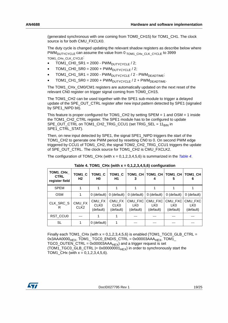
The configuration of TOM1_CHx (with x = 0,1,2,3,4,5,6) is summarized in the Table 4.
Finally each TOM1_CHx (with x = 0,1,2,3,4,5,6) is enabled (TOM1_TGC0_GLB_CTRL = 0x3AAA0000HEX, TOM1_ TGC0_ENDIS_CTRL = 0x00003AAAHEX, TOM1_ TGC0_OUTEN_CTRL = 0x00003AAAHEX) and a trigger request is set (TOM1_TGC0_GLB_CTRL |= 0x00000001HEX) in order to synchronously start the TOM1_CHx (with x = 0,1,2,3,4,5,6).
Table 4. TOM1_CHx (with x = 0,1,2,3,4,5,6) configuration
TOM1_CHx_CTRL
register field
TOM1_CH2
TOM1_CH0
TOM1_CH1
TOM1_CH3
TOM1_CH4
TOM1_CH5
TOM1_CH6
SPEM 1 1 1 1 1 1 1
OSM 1 0 (default) 0 (default) 0 (default) 0 (default) 0 (default) 0 (default)
CLK_SRC_SR
CMU_FXCLK2
CMU_FXCLK0
(default)
CMU_FXCLK0
(default)
CMU_FXCLK0
(default)
CMU_FXCLK0
(default)
CMU_FXCLK0
(default)
CMU_FXCLK0
(default)
RST_CCU0 --- 1 1 --- --- --- ---
SL 1 0 (default) 1 --- --- --- ---
Hardware and software implementation AN4688
20/25 DocID027795 Rev 1
3.9 TOM1_CH2 and SPE1 output update delayThe Timer Output Module (TOM) offers 16 independent channels to generate simple PWM signals at each output pin TOM[i]_CH[x]_OUT (i = 0,1,2; x = 0,1,2,..,14,15). For more details see the GTM specification document (see Section A.1: Reference documents, 3).
Detecting the zero crossing of the BEMF is only part of the sensorless operation of a BLDC motor. Once the zero crossing is detected, the 30 degree delay must be implemented. The delay time depends heavily on the rotor speed.
Acceleration and deceleration can also play an important role in determining the delay time. For this reason SPE1 output pattern update must be delayed using the TOM1_CH2 according to the rotor speed.
According to this, TIM0_CH3 interrupt service request is enabled (INTC0_PSR752 = 0x2002HEX, TIM0_CH3_IRQ_EN = 1BIN) and it is used to set the proper update delay for SPE1 output pattern for each mechanical revolution.
The update delay for SPE1 output, with TIM0_CH3_CLK_SEL = CMU_CLK1 = 1MHz and TOM1_CH2_CTRL_CLK_SRC_SR = CMU_FXCLK2 = 80MHz / 2^8 = 0,3125MHz, can be calculated as follow:
DELAYTOM1_CH2_CLK_CYCLE = (0x00FFFFFF & TIM0_CH3_GPR1) * 1000 / 3125 / 12
Moreover, the update of SPE1 could be synchronized with the beginning of PWM period in order to reduce the switching losses, in fact the high voltage spike occurring on each change of SPE1 output pattern is significantly reduced because only two low-side switches of the power stage are closed on each change of SPE1 output pattern.
According to this, considering TPWM = 50μs * 0,3125MHz = 15,625 TOM1_CH2_CLK_CYCLE, the synchronized delay can be calculated as follow:
DELAY_SYNCHTOM1_CH2_CLK_CYCLE = DELAYTOM1_CH2_CLK_CYCLE * 1000 / 15625 * 15625 / 1000
The double operations of multiplication and division with integer numbers are used in order to obtain an integer multiple of the TPWM. Finally, this value must be added a TPWM = 50μs * 0,3125MHz = 15,625TOM1_CH2_CLK_CYCLE with the subtraction of the SARADC injection delay TPWM/2 = 25μs plus the SARADC conversion time tconv = 3,600μs, i.e. the DELAYSARADC = 50μs - 25μs – 3,6μs * 0,3125MHz = 6,6875TOM1_CH2_CLK_CYCLE ≅
7TOM1_CH2_CLK_CYCLE. The calculated value DELAY_SYNCHTOM1_CH2_CLK_CYCLE is used to update the TOM1_CH2_CM0 and the TOM1_CH2_CM1 registers as follow:
TOM1_CH2_CM0 = 2 * DELAY_SYNCHTOM1_CH2_CLK_CYCLE
TOM1_CH2_CM1 = DELAY_SYNCHTOM1_CH2_CLK_CYCLE
3.10 Speed evaluation and controlEach TIM0_CHx (with x = 3,4,5) is configured in TPWM mode in order to measure the period and the duty cycle of the input signal.
The DSL bit defines the polarity of the PWM input signal. Setting DSL = 1BIN the high level time is measured as duty cycle and the TIM channel starts measuring after the rising edge occurrence.
Measurement is done using TIM0_CHx_CNT register counting with the configured clock coming from CMU_CLK1 until a falling edge occurrence. Then the counter value is stored
DocID027795 Rev 1 21/25
AN4688 Hardware and software implementation
23
inside the shadow register TIM0_CHx_CNTS (if CNTS_SEL = 0 BIN) and the counter TIM0_CHx_CNT counts continuously until the next rising edge occurrence. On this following rising edge occurrence the content of the TIM0_CHx_CNTS register is transferred to TIM0_CHx_GPR0 and the content of TIM0_CHx_CNT register is transferred to TIM0_CHx_GPR1, assuming settings for the selectors GPR0_SEL=11BIN and GPR1_SEL=11BIN. According to this, TIM0_CHx_GPR0 contains the duty cycle length and TIM0_CHx_GPR1 contains the period. The bits 1 to 7 of the TIM0_CHx_ECNT may be used to check data consistency of the registers TIM0_CHx_GPR0 and TIM0_CHx_GPR1.
According to this, the rotor speed, with TIM0_CH3_CLK_SEL = CMU_CLK1 = 1MHz, can be calculated in every speed loop control period as follow:
ROTOR_SPEED_BACKEMFRPM = 60000000DEC / (0x00FFFFFFHEX & TIM0_CH3_GPR1)
The speed loop control is provided by a PI controller called in every speed loop control period. The speed loop control period is fixed and independent from the rotor speed. The KP and KI constants are calculated from either the BLDC motor or the whole mechanical system.
Conclusion AN4688
22/25 DocID027795 Rev 1
4 Conclusion
The described implementation shows simplicity and efficiency on using of the SPC574K72xx device for BLDC motor control and, using the GTM module, the SPC574K72xx device is able to drive a BLDC motor in an automatic way both for sensored control (using Hall sensors feedback) and sensorless control (using BEMF feedback) with a CPU load close to zero.
DocID027795 Rev 1 23/25
AN4688 Further information
23
Appendix A Further information
A.1 Reference documents1. J. Shao, D. Nolan and T. Hopkins. A Novel Direct Back EMF Detection for Sensorless.
s.l.: IEEE, 2002. Vol. APEC, pp. 33-38.
2. SPC57XXMB evaluation system for SPC57x and SPC58x microcontroller families (DB2609, DocID027967)
3. BOSCH. GTM-IP Specification Rev. 1.5.5.1. 2013.
4. SPC574Kxx - 32-bit Power Architecture® based MCU with up to 4 Mbyte Flash and 304 Kbyte RAM memories (RM0334, DocID023671).
A.2 Terms and abbreviationsThis document uses the following terms and abbreviations.
Table 5. Acronyms
Terms Description
AEIGTM Generic Bus Interface
ARU Advanced Routing Unit
ATOM ARU-connected Timer Output Module
BEMF Back Electro Magnetic Force
CMU Clock Management Unit
GTM Generic Timer Module
IP Intellectual Property
PWM Pulse Width Modulation
SARADCSuccessive Approximation Register Analog-to-Digital Converter
SoC System on Chip
SPESensor Pattern Evaluation
TIM Timer Input Module
TOM Timer Output Module
UDCBUS Power Supply Voltage
Revision history AN4688
24/25 DocID027795 Rev 1
Revision history
Table 6. Document revision history
Date Revision Changes
07-Mar-2016 1 Initial release.

DocID027795 Rev 1 25/25
AN4688
25
IMPORTANT NOTICE – PLEASE READ CAREFULLY
STMicroelectronics NV and its subsidiaries (“ST”) reserve the right to make changes, corrections, enhancements, modifications, and improvements to ST products and/or to this document at any time without notice. Purchasers should obtain the latest relevant information on ST products before placing orders. ST products are sold pursuant to ST’s terms and conditions of sale in place at the time of order acknowledgement.
Purchasers are solely responsible for the choice, selection, and use of ST products and ST assumes no liability for application assistance or the design of Purchasers’ products.
No license, express or implied, to any intellectual property right is granted by ST herein.
Resale of ST products with provisions different from the information set forth herein shall void any warranty granted by ST for such product.
ST and the ST logo are trademarks of ST. All other product or service names are the property of their respective owners.
Information in this document supersedes and replaces information previously supplied in any prior versions of this document.
© 2016 STMicroelectronics – All rights reserved
Related Documents