Scalable and Low Cost Design Approach for Variable Block Size Motion Estimation Hadi Afshar, Philip Brisk, Paolo Ienne EPFL 30 April 2009

Welcome message from author
This document is posted to help you gain knowledge. Please leave a comment to let me know what you think about it! Share it to your friends and learn new things together.
Transcript
Scalable and Low Cost Design Approach for Variable Block Size Motion Estimation
Scalable and Low Cost Design Approach for Variable Block Size Motion Estimation
Hadi Afshar, Philip Brisk, Paolo Ienne
EPFL
Hadi Afshar, Philip Brisk, Paolo Ienne
EPFL
30 April 2009
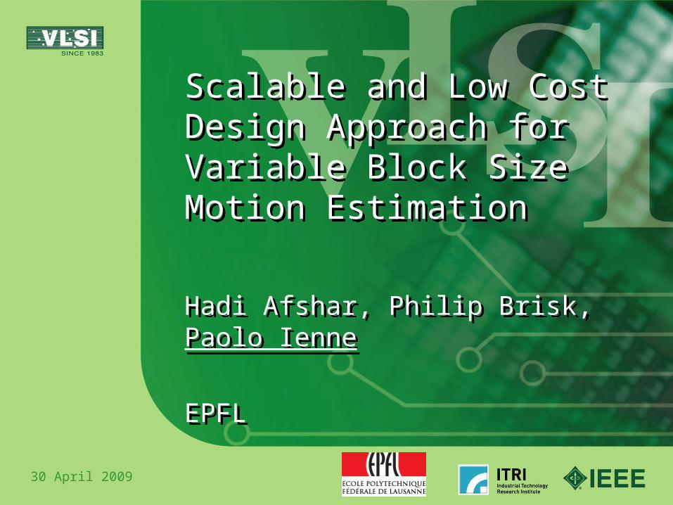
Fixed Block Size Motion Estimation Fixed Block Size Motion Estimation
Less compression Few motion vectors
Current FrameReference Frame
MBMV
MV: Motion VectorMB: Macro Block 2
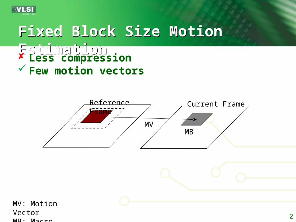
Variable Block Size Motion Estimation Variable Block Size Motion Estimation
More compression More motion vectors More computation
MBMV
Current FrameReference Frame
MV: Motion VectorMB: Macro Block 3
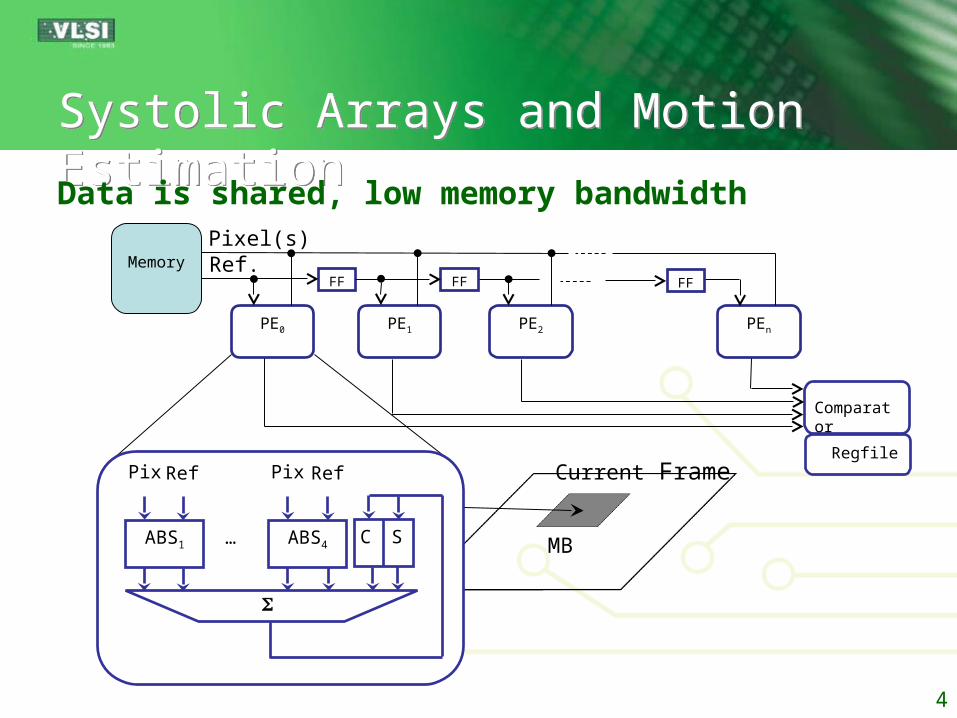
Systolic Arrays and Motion EstimationSystolic Arrays and Motion Estimation
Data is shared, low memory bandwidth
4
Current FrameReference Frame
MBMV
PE0 PE1 PE2 PEn
MemoryFF FF FF
Comparator
Regfile
Pixel(s)Ref.
C SABS1 ABS4…
Pix Ref Pix Ref
Comparator
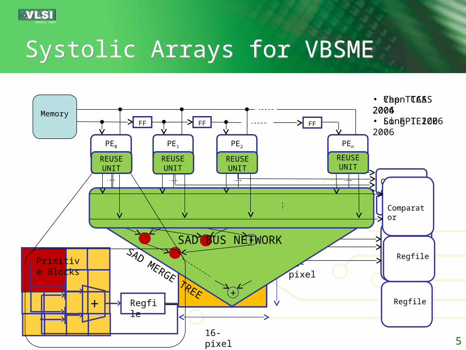
Systolic Arrays for VBSMESystolic Arrays for VBSME
PE0 PE1 PE2 PEn
MemoryFF FF FF
16-pixel
16-pixel
Regfile
Regfile
ComparatorSAD MERGE TREE
+ +++
+
Regfile
Comparator
SAD BUS NETWORK
REUSE UNIT
REUSE UNIT
REUSE UNIT
REUSE UNIT
Regfile+
Primitive Blocks
• Yap TCAS 2004• Song IEICE 2006• Chen TCAS 2006• Li FPT 2006
5
OutlineOutline
Proposed Design Approach Array Organization Processing Element Design Scheduling
Related WorkCase Study: H.264 VBSMEExperimental Results
VLSI Implementation FPGA Implementation
Conclusion6

Proposed ApproachProposed Approach
Basics: Each PE is augmented by a comparator
unit in addition to the reuse unit Each PE computes the SADs of all sub-
blocks within MB considering a specific reference MB
Each PE is one clock cycle prior to its neighbouring PE
Different PEs compute different SADs of the same MB with different reference MBs
7
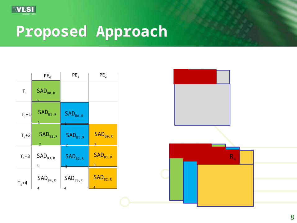
Proposed ApproachProposed Approach
SADB0,R0
PE2
Ti
Ti+1
Ti+2
Ti+3
PE0PE1
Ti+4
SADB1,R1
SADB2,R2
SADB3,R3
SADB4,R4
SADB0,R1
SADB1,R2
SADB2,R3
SADB3,R4
SADB0,R2
SADB1,R3
SADB2,R4
R0 R1 R3
B0 B1 B2
R2 R4
8
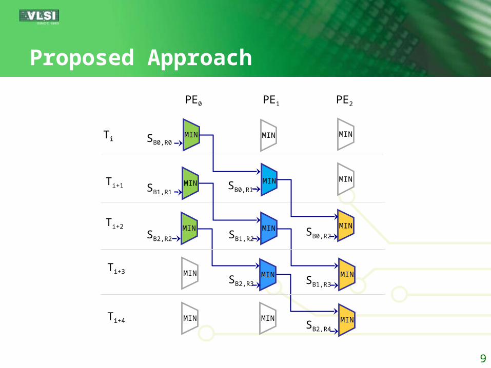
Proposed Approach
SB2,R2
SB1,R1
SB0,R0
PE2PE0 PE1
MIN MIN
MIN
MIN
MIN
MIN MIN
MIN MIN
MIN
MIN
MIN MIN
MIN
MINSB0,R1
SB1,R2
SB2,R3
SB0,R2
SB1,R3
SB2,R4
Ti
Ti+1
Ti+2
Ti+3
Ti+4
9
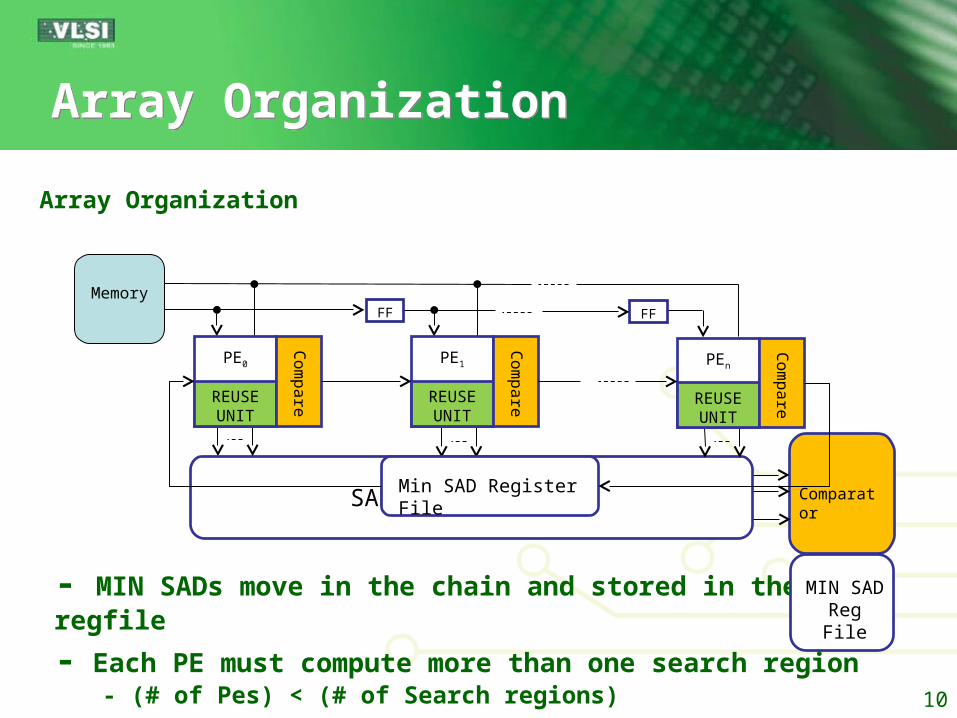
Array OrganizationArray Organization
MemoryFF FF
ComparatorSAD BUS NETWORK
REUSE UNIT
PE0
Co
mp
are REUSE
UNIT
PE1
Co
mp
are REUSE
UNIT
PEn
Co
mp
are
Min SAD Register File
Array Organization
- MIN SADs move in the chain and stored in the regfile
- Each PE must compute more than one search region- (# of Pes) < (# of Search regions)
MIN SADReg File
10
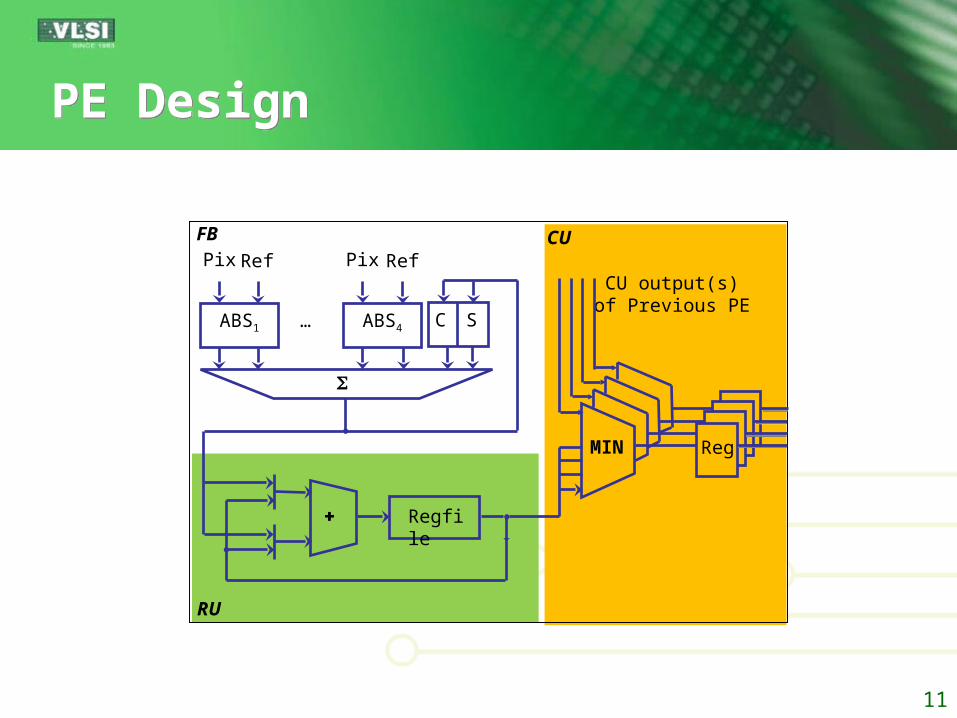
PE DesignPE Design
CU output(s) of Previous PE
C SABS1 ABS4…
Pix Ref Pix RefFB CU
RU
MIN Reg
Regfile
11
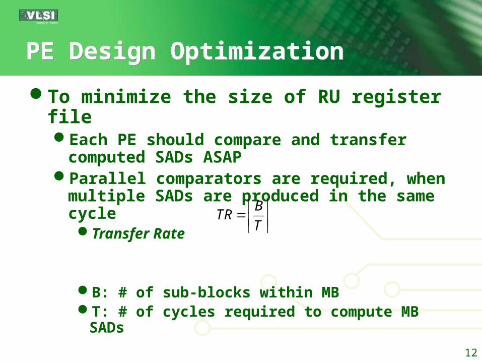
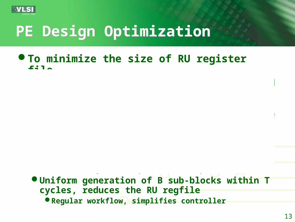
PE Design OptimizationPE Design Optimization
To minimize the size of RU register fileEach PE should compare and transfer computed
SADs ASAPParallel comparators are required, when multiple
SADs are produced in the same cycleTransfer Rate
B: # of sub-blocks within MBT: # of cycles required to compute MB SADs
BTR
T
12
PE Design OptimizationPE Design Optimization
To minimize the size of RU register fileEach PE should compare and transfer computed
SADs ASAPParallel comparators are required, when multiple
SADs are produced in the same cycleTransfer Rate
B: # of sub-blocks within MBT: # of cycles required to compute MB SADs
Uniform generation of B sub-blocks within T cycles, reduces the RU regfileRegular workflow, simplifies controller
BTR
T
13
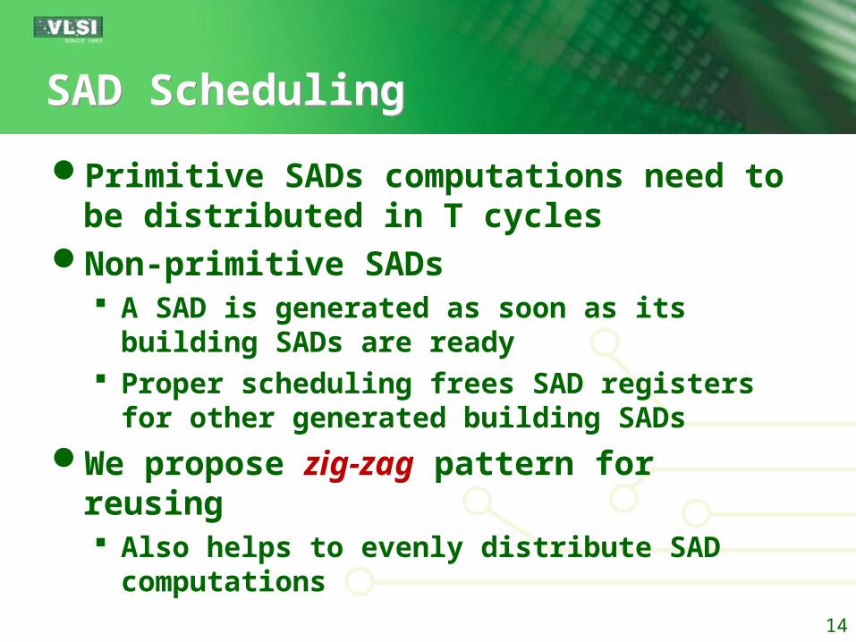
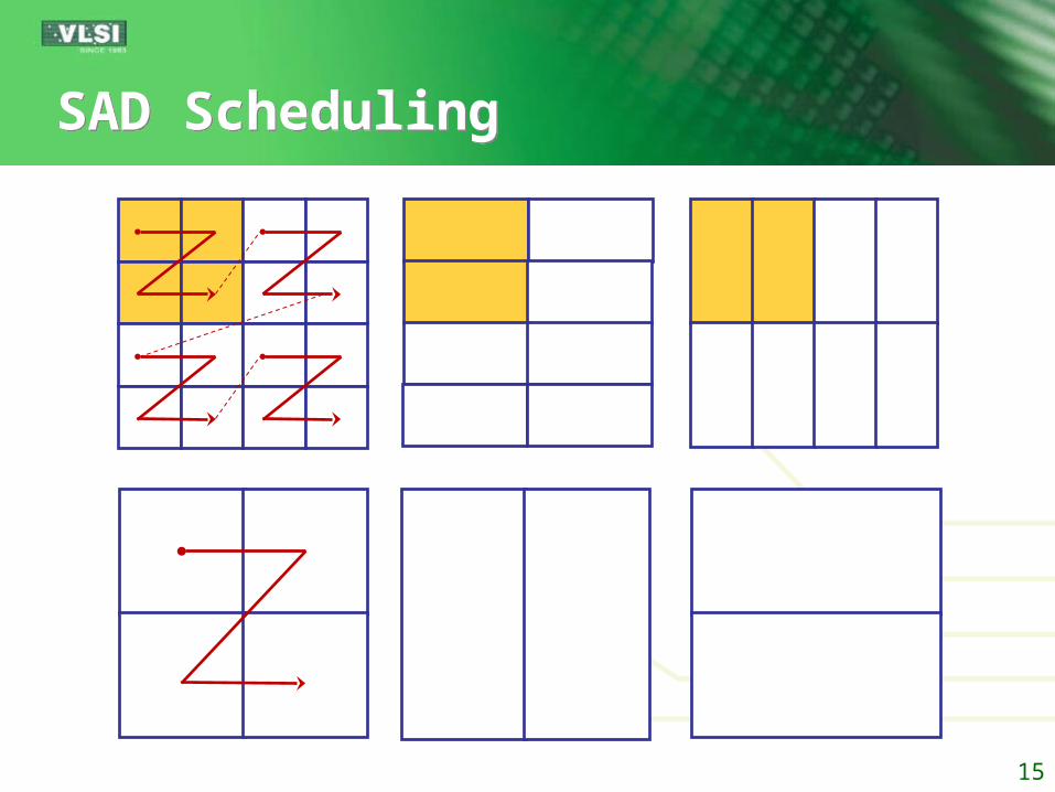
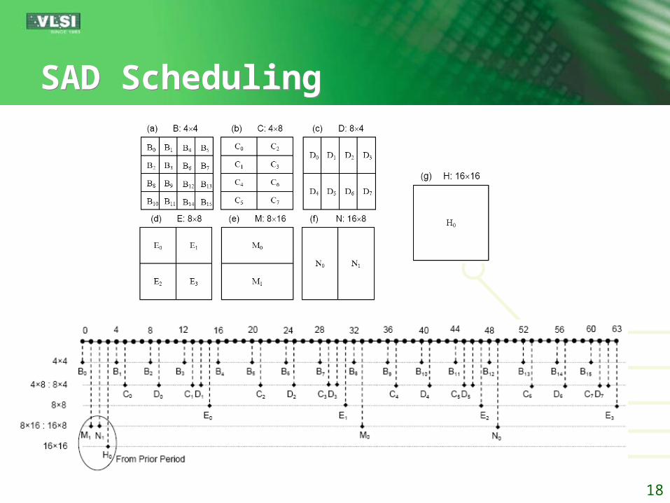
SAD SchedulingSAD Scheduling
Primitive SADs computations need to be distributed in T cycles
Non-primitive SADs A SAD is generated as soon as its building SADs
are ready Proper scheduling frees SAD registers for other
generated building SADs
We propose zig-zag pattern for reusing Also helps to evenly distribute SAD computations
14
SAD SchedulingSAD Scheduling
15
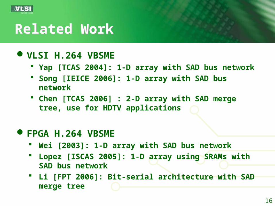
VLSI H.264 VBSME Yap [TCAS 2004]: 1-D array with SAD bus network Song [IEICE 2006]: 1-D array with SAD bus network Chen [TCAS 2006] : 2-D array with SAD merge tree, use for
HDTV applications
FPGA H.264 VBSME Wei [2003]: 1-D array with SAD bus network Lopez [ISCAS 2005]: 1-D array using SRAMs with SAD bus
network Li [FPT 2006]: Bit-serial architecture with SAD merge tree
Related WorkRelated Work
16
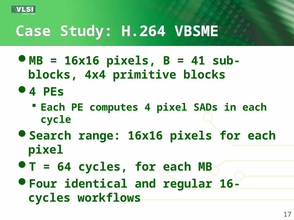
Case Study: H.264 VBSMECase Study: H.264 VBSME
MB = 16x16 pixels, B = 41 sub-blocks, 4x4 primitive blocks
4 PEs Each PE computes 4 pixel SADs in each cycle
Search range: 16x16 pixels for each pixel T = 64 cycles, for each MBFour identical and regular 16-cycles
workflows
17
18
SAD SchedulingSAD Scheduling
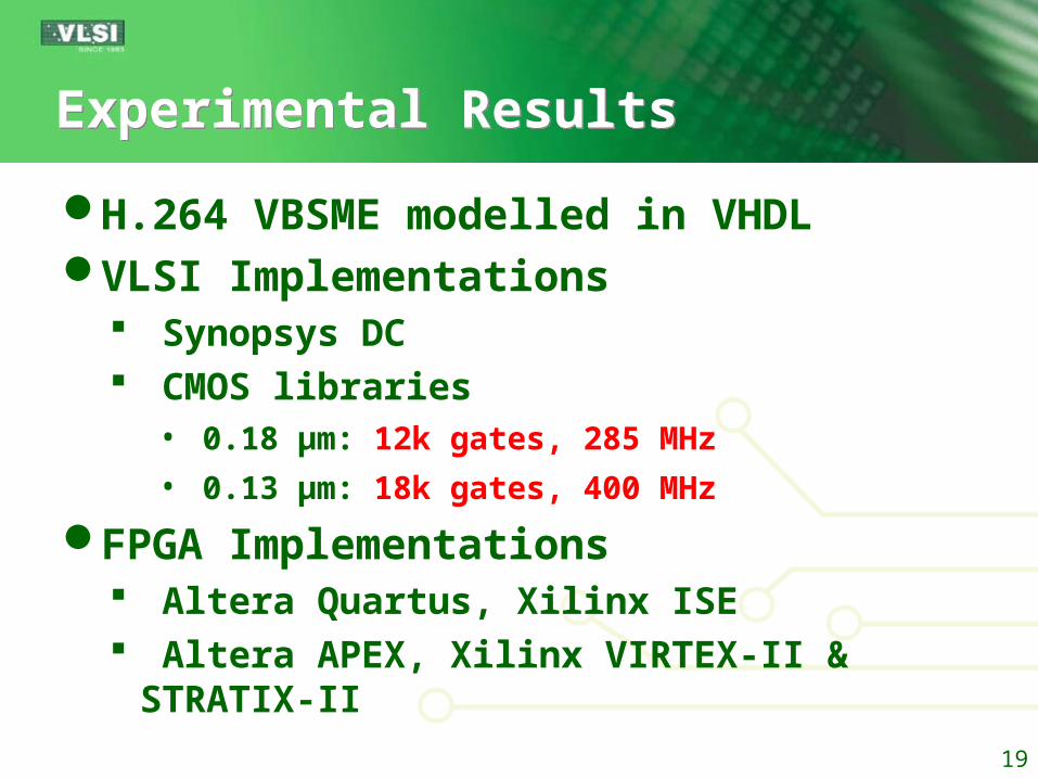
Experimental ResultsExperimental Results
H.264 VBSME modelled in VHDLVLSI Implementations
Synopsys DC CMOS libraries
• 0.18 µm: 12k gates, 285 MHz
• 0.13 µm: 18k gates, 400 MHz
FPGA Implementations Altera Quartus, Xilinx ISE Altera APEX, Xilinx VIRTEX-II & STRATIX-II
19
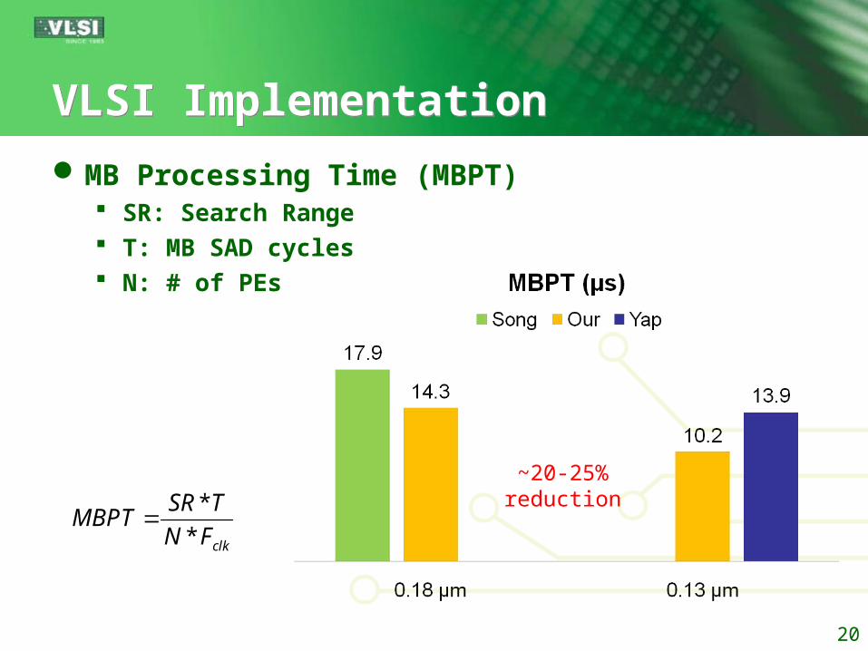
VLSI ImplementationVLSI Implementation
MB Processing Time (MBPT) SR: Search Range T: MB SAD cycles N: # of PEs
*
* clk
SR TMBPT
N F
20
~20-25%reduction
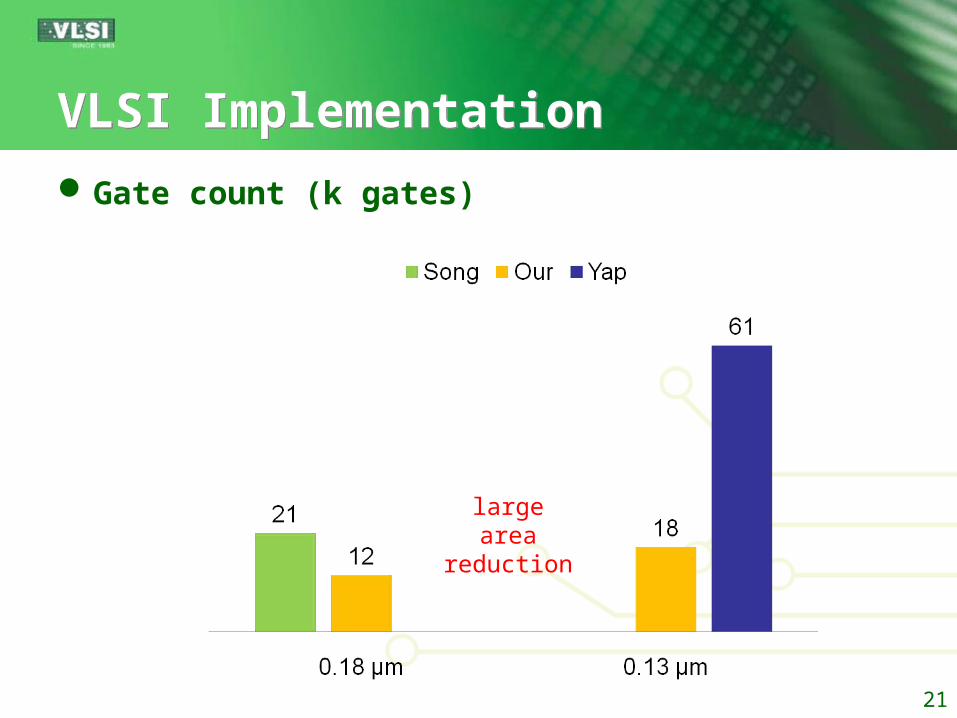
VLSI ImplementationVLSI Implementation
Gate count (k gates)
21
largearea
reduction
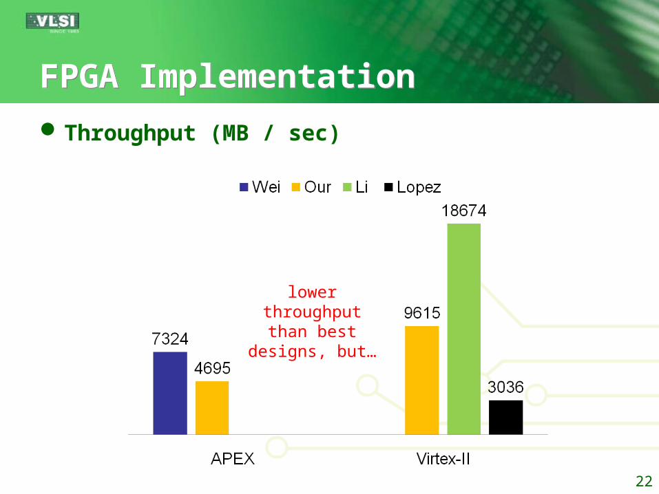
FPGA ImplementationFPGA Implementation
Throughput (MB / sec)
22
lowerthroughputthan best
designs, but…
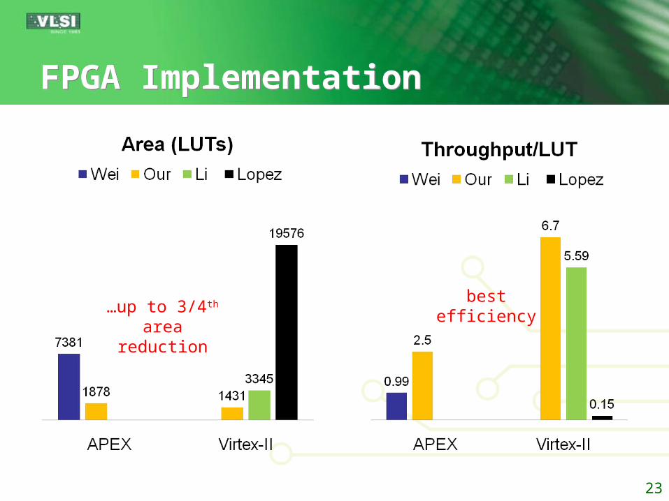
FPGA ImplementationFPGA Implementation
23
…up to 3/4th
areareduction
bestefficiency
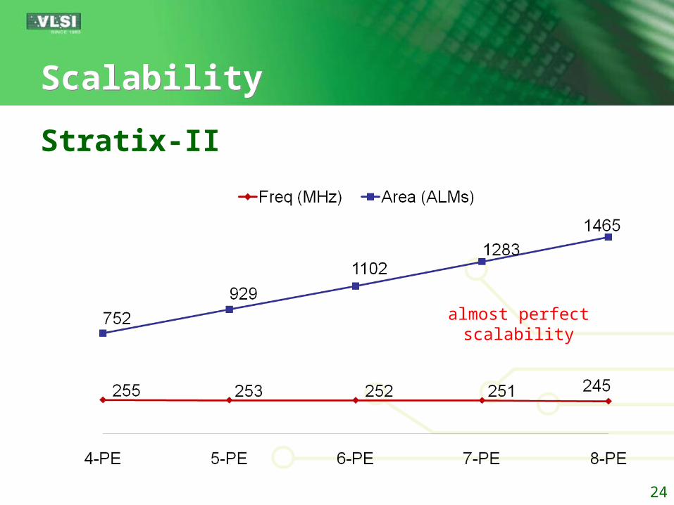
ScalabilityScalability
Stratix-II
24
almost perfectscalability
ConclusionConclusion
We improved scalability by redesigning the organization of systolic array and the design of PEs in the array Very low cost design, less area and delay
We proposed zig-zag pattern for reusing the primitive SADs Less registers for maintaining computed SADs Very regular workflow
This approach can be exploited by existing architectures and also can be applied to future standards with different block sizes
25
Thanks!
26

27
SAD SchedulingSAD Scheduling
Related Documents