Quad, 14-Bit, 80 MSPS/105 MSPS/125 MSPS Serial LVDS 1.8 V Analog-to-Digital Converter Data Sheet AD9253 Rev. A Document Feedback Information furnished by Analog Devices is believed to be accurate and reliable. However, no responsibility is assumed by Analog Devices for its use, nor for any infringements of patents or other rights of third parties that may result from its use. Specifications subject to change without notice. No license is granted by implication or otherwise under any patent or patent rights of Analog Devices. Trademarks and registered trademarks are the property of their respective owners. One Technology Way, P.O. Box 9106, Norwood, MA 02062-9106, U.S.A. Tel: 781.329.4700 ©2011–2014 Analog Devices, Inc. All rights reserved. Technical Support www.analog.com FEATURES 1.8 V supply operation Low power: 110 mW per channel at 125 MSPS with scalable power options SNR = 74 dB (to Nyquist) SFDR = 90 dBc (to Nyquist) DNL = ±0.75 LSB (typical); INL = ±2.0 LSB (typical) Serial LVDS (ANSI-644, default) and low power, reduced signal option (similar to IEEE 1596.3) 650 MHz full power analog bandwidth 2 V p-p input voltage range Serial port control Full chip and individual channel power-down modes Flexible bit orientation Built-in and custom digital test pattern generation Multichip sync and clock divider Programmable output clock and data alignment Programmable output resolution Standby mode APPLICATIONS Medical ultrasound High speed imaging Quadrature radio receivers Diversity radio receivers Test equipment GENERAL DESCRIPTION The AD9253 is a quad, 14-bit, 80 MSPS/105 MSPS/125 MSPS analog-to-digital converter (ADC) with an on-chip sample- and-hold circuit designed for low cost, low power, small size, and ease of use. The product operates at a conversion rate of up to 125 MSPS and is optimized for outstanding dynamic performance and low power in applications where a small package size is critical. The ADC requires a single 1.8 V power supply and LVPECL-/ CMOS-/LVDS-compatible sample rate clock for full performance operation. No external reference or driver components are required for many applications. The ADC automatically multiplies the sample rate clock for the appropriate LVDS serial data rate. A data clock output (DCO) for capturing data on the output and a frame clock output (FCO) for signaling a new output byte are provided. Individual-channel power-down is supported and typically consumes less than 2 mW when all channels are disabled. The ADC contains several features designed to maximize flexibility and minimize system cost, such FUNCTIONAL BLOCK DIAGRAM AD9253 10065-001 AVDD PDWN DRVDD REF SELECT VIN–A VIN+A VIN–B VIN+B VIN–D VIN+D VIN–C VIN+C SENSE AGND SYNC VCM VREF D0–A D0+A D0–B D0+B D1–B D1+B D1–C D1+C D0–C D0+C D1–D D1+D DCO– DCO+ D0–D D0+D FCO– FCO+ D1–A D1+A CLK+ CLK– CSB SDIO/OLM SCLK/DTP RBIAS PIPELINE ADC PIPELINE ADC PIPELINE ADC SERIAL LVDS DIGITAL SERIALIZER DIGITAL SERIALIZER DIGITAL SERIALIZER DIGITAL SERIALIZER CLOCK MANAGEMENT SERIAL PORT INTERFACE SERIAL LVDS SERIAL LVDS SERIAL LVDS SERIAL LVDS SERIAL LVDS SERIAL LVDS SERIAL LVDS PIPELINE ADC 14 14 14 14 1V Figure 1. as programmable output clock and data alignment and digital test pattern generation. The available digital test patterns include built-in deterministic and pseudorandom patterns, along with custom user-defined test patterns entered via the serial port interface (SPI). The AD9253 is available in a RoHS-compliant, 48-lead LFCSP. It is specified over the industrial temperature range of −40°C to +85°C. This product is protected by a U.S. patent. PRODUCT HIGHLIGHTS 1. Small Footprint. Four ADCs are contained in a small, space- saving package. 2. Low power of 110 mW/channel at 125 MSPS with scalable power options. 3. Pin compatible to the AD9633 12-bit quad ADC. 4. Ease of Use. A data clock output (DCO) operates at frequencies of up to 500 MHz and supports double data rate (DDR) operation. 5. User Flexibility. The SPI control offers a wide range of flexible features to meet specific system requirements.

Welcome message from author
This document is posted to help you gain knowledge. Please leave a comment to let me know what you think about it! Share it to your friends and learn new things together.
Transcript
Quad, 14-Bit, 80 MSPS/105 MSPS/125 MSPS Serial LVDS 1.8 V Analog-to-Digital Converter
Data Sheet AD9253
Rev. A Document Feedback Information furnished by Analog Devices is believed to be accurate and reliable. However, no responsibility is assumed by Analog Devices for its use, nor for any infringements of patents or other rights of third parties that may result from its use. Specifications subject to change without notice. No license is granted by implication or otherwise under any patent or patent rights of Analog Devices. Trademarks and registered trademarks are the property of their respective owners.
One Technology Way, P.O. Box 9106, Norwood, MA 02062-9106, U.S.A.Tel: 781.329.4700 ©2011–2014 Analog Devices, Inc. All rights reserved. Technical Support www.analog.com
FEATURES 1.8 V supply operation Low power: 110 mW per channel at 125 MSPS with scalable
power options SNR = 74 dB (to Nyquist) SFDR = 90 dBc (to Nyquist) DNL = ±0.75 LSB (typical); INL = ±2.0 LSB (typical) Serial LVDS (ANSI-644, default) and low power, reduced
signal option (similar to IEEE 1596.3) 650 MHz full power analog bandwidth 2 V p-p input voltage range Serial port control
Full chip and individual channel power-down modes Flexible bit orientation Built-in and custom digital test pattern generation Multichip sync and clock divider Programmable output clock and data alignment Programmable output resolution Standby mode
APPLICATIONS Medical ultrasound High speed imaging Quadrature radio receivers Diversity radio receivers Test equipment
GENERAL DESCRIPTION The AD9253 is a quad, 14-bit, 80 MSPS/105 MSPS/125 MSPS analog-to-digital converter (ADC) with an on-chip sample- and-hold circuit designed for low cost, low power, small size, and ease of use. The product operates at a conversion rate of up to 125 MSPS and is optimized for outstanding dynamic performance and low power in applications where a small package size is critical.
The ADC requires a single 1.8 V power supply and LVPECL-/ CMOS-/LVDS-compatible sample rate clock for full performance operation. No external reference or driver components are required for many applications.
The ADC automatically multiplies the sample rate clock for the appropriate LVDS serial data rate. A data clock output (DCO) for capturing data on the output and a frame clock output (FCO) for signaling a new output byte are provided. Individual-channel power-down is supported and typically consumes less than 2 mW when all channels are disabled. The ADC contains several features designed to maximize flexibility and minimize system cost, such
FUNCTIONAL BLOCK DIAGRAM
AD9253
1006
5-00
1
AVDD PDWN DRVDD
REFSELECT
VIN–AVIN+A
VIN–BVIN+B
VIN–DVIN+D
VIN–CVIN+C
SENSE
AGND
SYN
C
VCM
VREF
D0–AD0+A
D0–BD0+B
D1–BD1+B
D1–CD1+CD0–CD0+C
D1–DD1+D
DCO–DCO+
D0–DD0+D
FCO–FCO+
D1–AD1+A
CLK
+
CLK
–
CSB
SDIO
/OLM
SCLK
/DTP
RBIAS
PIPELINEADC
PIPELINEADC
PIPELINEADC
SERIALLVDSDIGITAL
SERIALIZER
DIGITALSERIALIZER
DIGITALSERIALIZER
DIGITALSERIALIZER
CLOCKMANAGEMENT
SERIAL PORTINTERFACE
SERIALLVDS
SERIALLVDS
SERIALLVDS
SERIALLVDS
SERIALLVDS
SERIALLVDS
SERIALLVDS
PIPELINEADC
14
14
14
14
1V
Figure 1.
as programmable output clock and data alignment and digital test pattern generation. The available digital test patterns include built-in deterministic and pseudorandom patterns, along with custom user-defined test patterns entered via the serial port interface (SPI).
The AD9253 is available in a RoHS-compliant, 48-lead LFCSP. It is specified over the industrial temperature range of −40°C to +85°C. This product is protected by a U.S. patent.
PRODUCT HIGHLIGHTS 1. Small Footprint. Four ADCs are contained in a small, space-
saving package. 2. Low power of 110 mW/channel at 125 MSPS with scalable
power options. 3. Pin compatible to the AD9633 12-bit quad ADC. 4. Ease of Use. A data clock output (DCO) operates at
frequencies of up to 500 MHz and supports double data rate (DDR) operation.
5. User Flexibility. The SPI control offers a wide range of flexible features to meet specific system requirements.
AD9253 Data Sheet
TABLE OF CONTENTS Features .............................................................................................. 1 Applications ....................................................................................... 1 General Description ......................................................................... 1 Functional Block Diagram .............................................................. 1 Product Highlights ........................................................................... 1 Revision History ............................................................................... 2 Specifications ..................................................................................... 3
DC Specifications ......................................................................... 3 AC Specifications .......................................................................... 4 Digital Specifications ................................................................... 5 Switching Specifications .............................................................. 6 Timing Specifications .................................................................. 6
Absolute Maximum Ratings .......................................................... 10 Thermal Resistance .................................................................... 10 ESD Caution ................................................................................ 10
Pin Configuration and Function Descriptions ........................... 11 Typical Performance Characteristics ........................................... 13
AD9253-80 .................................................................................. 13 AD9253-105 ................................................................................ 15 AD9253-125 ................................................................................ 17
Equivalent Circuits ......................................................................... 20 Theory of Operation ...................................................................... 21
Analog Input Considerations .................................................... 21 Voltage Reference ....................................................................... 22
Clock Input Considerations ...................................................... 23 Power Dissipation and Power-Down Mode ........................... 25 Digital Outputs and Timing ..................................................... 26 Output Test Modes ..................................................................... 29
Serial Port Interface (SPI) .............................................................. 30 Configuration Using the SPI ..................................................... 30 Hardware Interface ..................................................................... 31 Configuration Without the SPI ................................................ 31 SPI Accessible Features .............................................................. 31
Memory Map .................................................................................. 32 Reading the Memory Map Register Table ............................... 32 Memory Map Register Table ..................................................... 33 Memory Map Register Descriptions ........................................ 36
Applications Information .............................................................. 38 Design Guidelines ...................................................................... 38 Power and Ground Recommendations ................................... 38 Clock Stability Considerations ................................................. 38 Exposed Pad Thermal Heat Slug Recommendations ............ 38 VCM ............................................................................................. 38 Reference Decoupling ................................................................ 38 SPI Port ........................................................................................ 38 Crosstalk Performance .............................................................. 39
Outline Dimensions ....................................................................... 40 Ordering Guide .......................................................................... 40
REVISION HISTORY 9/14—Rev. 0 to Rev. A
Changes to Table 2 ............................................................................ 4 Added Propagation Delay Parameters of 1.5 ns (Min) and 3.1 ns (Max); Table 4, Changed tSSYNC from 0.24 ns Typ to 1.2 ns Min, and Changed tHSYNC from 0.40 ns Typ to −0.2 ns Min; Table 5 ......................................................................... 6 Changes to Figure 3 .......................................................................... 7 Changes to Figure 5 .......................................................................... 8 Changes to Pin 9 to Pin 14 and Pin 23 to Pin 28 Descriptions .. 11 Changes to Figure 48 and Figure 49 ............................................. 20 Changes to Clock Input Options Section .................................... 23
Changes to Jitter Considerations Section .................................... 25 Changes to Digital Outputs and Timing Section ....................... 26 Changes to Table 11 ....................................................................... 28 Changes to Table 12 ....................................................................... 29 Changes to Channel-Specific Registers Section ......................... 32 Changes to Output Phase (Register 0x16) Section .................... 36 Changes to Resolution/Sample Rate Override (Register 0x100) Section .............................................................................................. 37 Added Clock Stability Considerations Section........................... 38 Updated Outline Dimensions ....................................................... 40
10/11—Revision 0: Initial Version
Rev. A | Page 2 of 40
Data Sheet AD9253
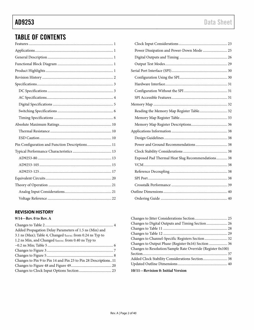
SPECIFICATIONS DC SPECIFICATIONS AVDD = 1.8 V, DRVDD = 1.8 V, 2 V p-p differential input, 1.0 V internal reference, AIN = −1.0 dBFS, unless otherwise noted.
Table 1.
Parameter1 Temp AD9253-80 AD9253-105 AD9253-125
Min Typ Max Min Typ Max Min Typ Max Unit RESOLUTION 14 14 14 Bits ACCURACY
No Missing Codes Full Guaranteed Guaranteed Guaranteed Offset Error Full −0.7 −0.3 +0.1 −0.7 −0.3 +0.1 −0.7 −0.3 +0.1 % FSR Offset Matching Full −0.6 +0.2 +0.6 −0.6 +0.2 +0.6 −0.6 +0.2 +0.6 % FSR Gain Error Full −10 −5 0 −10 −5 0 −10 −5 0 % FSR Gain Matching Full 1 1.6 1 1.6 1.1 1.6 % FSR Differential Nonlinearity (DNL) Full −1 +1.6 −0.8 +1.5 −0.8 +1.5 LSB 25°C ±0.8 ±0.75 ±0.75 LSB Integral Nonlinearity (INL) Full −4.0 +4.0 −4.0 4.0 −4.0 +4.0 LSB 25°C ±1.5 ±2.0 ±2.0 LSB
TEMPERATURE DRIFT Offset Error Full ±2 ±2 ±2 ppm/°C
INTERNAL VOLTAGE REFERENCE Output Voltage (1 V Mode) Full 0.98 1.0 1.02 0.98 1.0 1.02 0.98 1.0 1.02 V Load Regulation at 1.0 mA (VREF = 1 V) Full 2 2 2 mV Input Resistance Full 7.5 7.5 7.5 kΩ
INPUT-REFERRED NOISE
VREF = 1.0 V 25°C 0.94 0.94 0.94 LSB rms
ANALOG INPUTS Differential Input Voltage (VREF = 1 V) Full 2 2 2 V p-p Common-Mode Voltage Full 0.9 0.9 0.9 V Differential Input Resistance 5.2 5.2 5.2 kΩ Differential Input Capacitance Full 3.5 3.5 3.5 pF
POWER SUPPLY AVDD Full 1.7 1.8 1.9 1.7 1.8 1.9 1.7 1.8 1.9 V DRVDD Full 1.7 1.8 1.9 1.7 1.8 1.9 1.7 1.8 1.9 V IAVDD
2 Full 131 144 158 172 183 200 mA IDRVDD (ANSI-644 Mode)2 Full 63 81 67 95 71 100 mA IDRVDD (Reduced Range Mode)2 25°C 42 48 53 mA
TOTAL POWER CONSUMPTION DC Input Full 326 375 423 mW Sine Wave Input (Four Channels Including
Output Drivers ANSI-644 Mode) Full 349 405 405 481 457 540 mW
Sine Wave Input (Four Channels Including Output Drivers Reduced Range Mode)
25°C 311 371 425 mW
Power-Down Full 2 2 2 mW Standby3 Full 178 209 236 mW
1 See the AN-835 Application Note, Understanding High Speed ADC Testing and Evaluation, for definitions and for details on how these tests were completed. 2 Measured with a low input frequency, full-scale sine wave on all four channels. 3 Can be controlled via the SPI.
Rev. A | Page 3 of 40
AD9253 Data Sheet
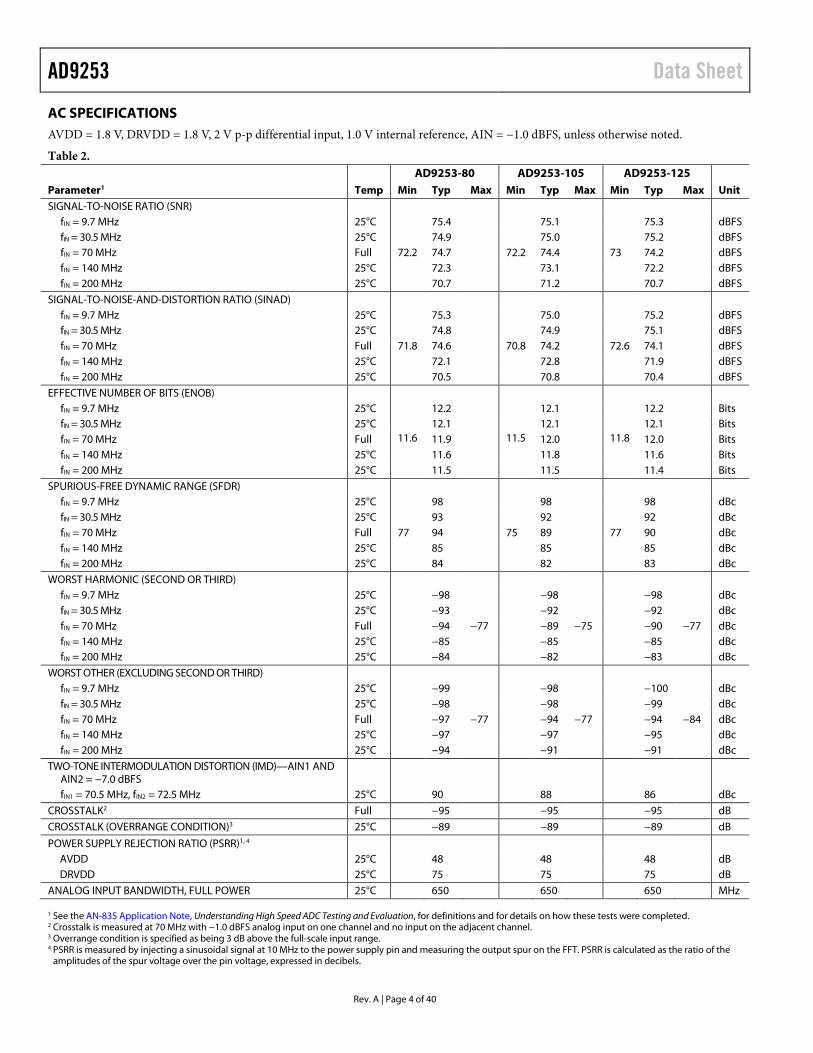
AC SPECIFICATIONS AVDD = 1.8 V, DRVDD = 1.8 V, 2 V p-p differential input, 1.0 V internal reference, AIN = −1.0 dBFS, unless otherwise noted.
Table 2.
Parameter1 Temp
AD9253-80 AD9253-105 AD9253-125 Unit Min Typ Max Min Typ Max Min Typ Max
SIGNAL-TO-NOISE RATIO (SNR) fIN = 9.7 MHz 25°C 75.4 75.1 75.3 dBFS fIN = 30.5 MHz 25°C 74.9 75.0 75.2 dBFS fIN = 70 MHz Full 72.2 74.7 72.2 74.4 73 74.2 dBFS fIN = 140 MHz 25°C 72.3 73.1 72.2 dBFS fIN = 200 MHz 25°C 70.7 71.2 70.7 dBFS
SIGNAL-TO-NOISE-AND-DISTORTION RATIO (SINAD) fIN = 9.7 MHz 25°C 75.3 75.0 75.2 dBFS fIN = 30.5 MHz 25°C 74.8 74.9 75.1 dBFS fIN = 70 MHz Full 71.8 74.6 70.8 74.2 72.6 74.1 dBFS fIN = 140 MHz 25°C 72.1 72.8 71.9 dBFS fIN = 200 MHz 25°C 70.5 70.8 70.4 dBFS
EFFECTIVE NUMBER OF BITS (ENOB) fIN = 9.7 MHz 25°C 12.2 12.1 12.2 Bits fIN = 30.5 MHz 25°C 12.1 12.1 12.1 Bits fIN = 70 MHz Full 11.6 11.9 11.5 12.0 11.8 12.0 Bits fIN = 140 MHz 25°C 11.6 11.8 11.6 Bits fIN = 200 MHz 25°C 11.5 11.5 11.4 Bits
SPURIOUS-FREE DYNAMIC RANGE (SFDR) fIN = 9.7 MHz 25°C 98 98 98 dBc fIN = 30.5 MHz 25°C 93 92 92 dBc fIN = 70 MHz Full 77 94 75 89 77 90 dBc fIN = 140 MHz 25°C 85 85 85 dBc fIN = 200 MHz 25°C 84 82 83 dBc
WORST HARMONIC (SECOND OR THIRD) fIN = 9.7 MHz 25°C −98 −98 −98 dBc fIN = 30.5 MHz 25°C −93 −92 −92 dBc fIN = 70 MHz Full −94 −77 −89 −75 −90 −77 dBc fIN = 140 MHz 25°C −85 −85 −85 dBc fIN = 200 MHz 25°C −84 −82 −83 dBc
WORST OTHER (EXCLUDING SECOND OR THIRD) fIN = 9.7 MHz 25°C −99 −98 −100 dBc fIN = 30.5 MHz 25°C −98 −98 −99 dBc fIN = 70 MHz Full −97 −77 −94 −77 −94 −84 dBc fIN = 140 MHz 25°C −97 −97 −95 dBc fIN = 200 MHz 25°C −94 −91 −91 dBc
TWO-TONE INTERMODULATION DISTORTION (IMD)—AIN1 AND AIN2 = −7.0 dBFS
fIN1 = 70.5 MHz, fIN2 = 72.5 MHz 25°C 90 88 86 dBc
CROSSTALK2 Full −95 −95 −95 dB
CROSSTALK (OVERRANGE CONDITION)3 25°C −89 −89 −89 dB
POWER SUPPLY REJECTION RATIO (PSRR)1, 4
AVDD 25°C 48 48 48 dB DRVDD 25°C 75 75 75 dB
ANALOG INPUT BANDWIDTH, FULL POWER 25°C 650 650 650 MHz
1 See the AN-835 Application Note, Understanding High Speed ADC Testing and Evaluation, for definitions and for details on how these tests were completed. 2 Crosstalk is measured at 70 MHz with −1.0 dBFS analog input on one channel and no input on the adjacent channel. 3 Overrange condition is specified as being 3 dB above the full-scale input range. 4 PSRR is measured by injecting a sinusoidal signal at 10 MHz to the power supply pin and measuring the output spur on the FFT. PSRR is calculated as the ratio of the
amplitudes of the spur voltage over the pin voltage, expressed in decibels.
Rev. A | Page 4 of 40
Data Sheet AD9253
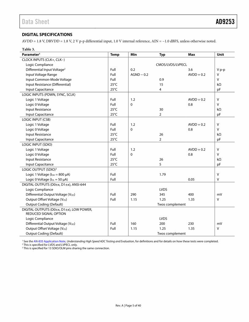
DIGITAL SPECIFICATIONS AVDD = 1.8 V, DRVDD = 1.8 V, 2 V p-p differential input, 1.0 V internal reference, AIN = −1.0 dBFS, unless otherwise noted.
Table 3. Parameter1 Temp Min Typ Max Unit CLOCK INPUTS (CLK+, CLK−)
Logic Compliance CMOS/LVDS/LVPECL Differential Input Voltage2 Full 0.2 3.6 V p-p Input Voltage Range Full AGND − 0.2 AVDD + 0.2 V Input Common-Mode Voltage Full 0.9 V Input Resistance (Differential) 25°C 15 kΩ Input Capacitance 25°C 4 pF
LOGIC INPUTS (PDWN, SYNC, SCLK) Logic 1 Voltage Full 1.2 AVDD + 0.2 V Logic 0 Voltage Full 0 0.8 V Input Resistance 25°C 30 kΩ Input Capacitance 25°C 2 pF
LOGIC INPUT (CSB) Logic 1 Voltage Full 1.2 AVDD + 0.2 V Logic 0 Voltage Full 0 0.8 V Input Resistance 25°C 26 kΩ Input Capacitance 25°C 2 pF
LOGIC INPUT (SDIO) Logic 1 Voltage Full 1.2 AVDD + 0.2 V Logic 0 Voltage Full 0 0.8 V Input Resistance 25°C 26 kΩ Input Capacitance 25°C 5 pF
LOGIC OUTPUT (SDIO)3 Logic 1 Voltage (IOH = 800 μA) Full 1.79 V Logic 0 Voltage (IOL = 50 μA) Full 0.05 V
DIGITAL OUTPUTS (D0±x, D1±x), ANSI-644 Logic Compliance LVDS Differential Output Voltage (VOD) Full 290 345 400 mV Output Offset Voltage (VOS) Full 1.15 1.25 1.35 V Output Coding (Default) Twos complement
DIGITAL OUTPUTS (D0±x, D1±x), LOW POWER, REDUCED SIGNAL OPTION
Logic Compliance LVDS Differential Output Voltage (VOD) Full 160 200 230 mV Output Offset Voltage (VOS) Full 1.15 1.25 1.35 V Output Coding (Default) Twos complement
1 See the AN-835 Application Note, Understanding High Speed ADC Testing and Evaluation, for definitions and for details on how these tests were completed. 2 This is specified for LVDS and LVPECL only. 3 This is specified for 13 SDIO/OLM pins sharing the same connection.
Rev. A | Page 5 of 40
AD9253 Data Sheet
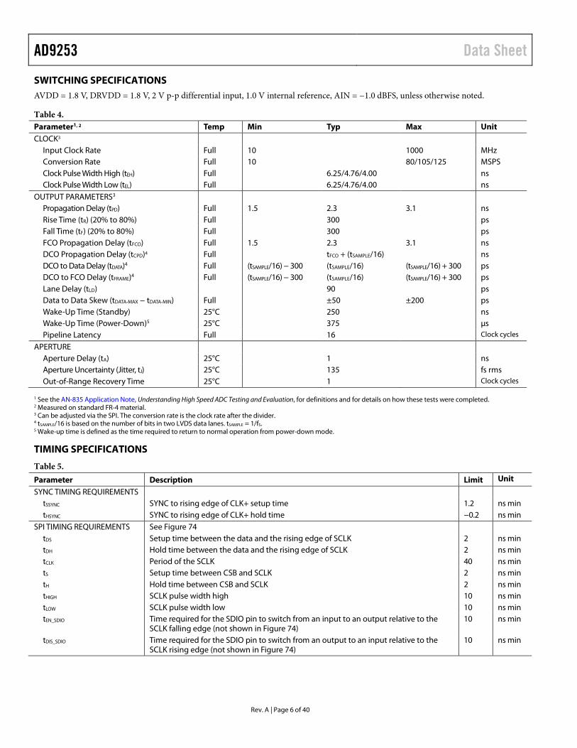
SWITCHING SPECIFICATIONS AVDD = 1.8 V, DRVDD = 1.8 V, 2 V p-p differential input, 1.0 V internal reference, AIN = −1.0 dBFS, unless otherwise noted.
Table 4. Parameter1, 2 Temp Min Typ Max Unit CLOCK3
Input Clock Rate Full 10 1000 MHz Conversion Rate Full 10 80/105/125 MSPS Clock Pulse Width High (tEH) Full 6.25/4.76/4.00 ns Clock Pulse Width Low (tEL) Full 6.25/4.76/4.00 ns
OUTPUT PARAMETERS3 Propagation Delay (tPD) Full 1.5 2.3 3.1 ns Rise Time (tR) (20% to 80%) Full 300 ps Fall Time (tF) (20% to 80%) Full 300 ps FCO Propagation Delay (tFCO) Full 1.5 2.3 3.1 ns DCO Propagation Delay (tCPD)4 Full tFCO + (tSAMPLE/16) ns DCO to Data Delay (tDATA)4 Full (tSAMPLE/16) − 300 (tSAMPLE/16) (tSAMPLE/16) + 300 ps DCO to FCO Delay (tFRAME)4 Full (tSAMPLE/16) − 300 (tSAMPLE/16) (tSAMPLE/16) + 300 ps Lane Delay (tLD) 90 ps Data to Data Skew (tDATA-MAX − tDATA-MIN) Full ±50 ±200 ps Wake-Up Time (Standby) 25°C 250 ns Wake-Up Time (Power-Down)5 25°C 375 μs Pipeline Latency Full 16 Clock cycles
APERTURE Aperture Delay (tA) 25°C 1 ns Aperture Uncertainty (Jitter, tJ) 25°C 135 fs rms Out-of-Range Recovery Time 25°C 1 Clock cycles
1 See the AN-835 Application Note, Understanding High Speed ADC Testing and Evaluation, for definitions and for details on how these tests were completed. 2 Measured on standard FR-4 material. 3 Can be adjusted via the SPI. The conversion rate is the clock rate after the divider. 4 tSAMPLE/16 is based on the number of bits in two LVDS data lanes. tSAMPLE = 1/fS. 5 Wake-up time is defined as the time required to return to normal operation from power-down mode.
TIMING SPECIFICATIONS
Table 5. Parameter Description Limit Unit
SYNC TIMING REQUIREMENTS tSSYNC SYNC to rising edge of CLK+ setup time 1.2 ns min tHSYNC SYNC to rising edge of CLK+ hold time −0.2 ns min
SPI TIMING REQUIREMENTS See Figure 74 tDS Setup time between the data and the rising edge of SCLK 2 ns min tDH Hold time between the data and the rising edge of SCLK 2 ns min tCLK Period of the SCLK 40 ns min tS Setup time between CSB and SCLK 2 ns min tH Hold time between CSB and SCLK 2 ns min tHIGH SCLK pulse width high 10 ns min tLOW SCLK pulse width low 10 ns min tEN_SDIO Time required for the SDIO pin to switch from an input to an output relative to the
SCLK falling edge (not shown in Figure 74) 10 ns min
tDIS_SDIO Time required for the SDIO pin to switch from an output to an input relative to the SCLK rising edge (not shown in Figure 74)
10 ns min
Rev. A | Page 6 of 40
Data Sheet AD9253
Rev. A | Page 7 of 40
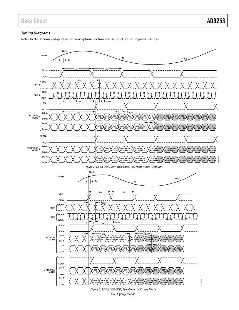
Timing Diagrams
Refer to the Memory Map Register Descriptions section and Table 21 for SPI register settings.
D0–A
D0+A
D1–A
D1+A
FCO–
BYTEWISEMODE
FCO+
D0–A
D0+A
D1–A
D1+A
FCO–
DCO–
DCO+
DCO+
CLK+
VIN±x
CLK–
DCO–
FCO+
BITWISEMODE
SDR
DDR
1006
5-00
3
MSBN – 17
D12N – 17
D11N – 17
D10N – 17
D09N – 17
D08N – 17
D07N – 17
D06N – 17
MSBN – 16
D12N – 16
D11N – 16
D10N – 16
D09N – 16
D08N – 16
D07N – 16
D06N – 16
D05N – 17
D04N – 17
D03N – 17
D02N – 17
D01N – 17
LSBN – 17
0N – 17
0N – 17
D05N – 16
D04N – 16
D03N – 16
D02N – 16
D01N – 16
LSBN – 16
0N – 16
0N – 16
MSBN – 17
D11N – 17
D09N – 17
D07N – 17
D05N – 17
D03N – 17
D01N – 17
0N – 17
MSBN – 16
D11N – 16
D09N – 16
D07N – 16
D05N – 16
D03N – 16
D01N – 16
0N – 16
D12N – 17
D10N – 17
D08N – 17
D06N – 17
D04N – 17
D02N – 17
LSBN – 17
0N – 17
D12N – 16
D10N – 16
D08N – 16
D06N – 16
D04N – 16
D02N – 16
LSBN – 16
0N – 16
tA
tDATA
tLD
tEH
tFCO tFRAME
tPD
tCPD
tEL
N – 1
N N + 1
Figure 2. 16-Bit DDR/SDR, Two-Lane, 1× Frame Mode (Default)
1006
5-00
4
D0–A
D0+AD1–A
D1+A
FCO–
BYTEWISEMODE
FCO+
D0–A
D0+A
D1–A
D1+A
FCO–
DCO–
CLK+
CLK–
DCO+
DCO–
DCO+
FCO+
BITWISEMODE
SDR
DDR
D10N – 16
D08N – 16
D06N – 16
D04N – 16
D02N – 16
LSBN – 16
D10N – 17
D08N – 17
D06N – 17
D04N – 17
D02N – 17
LSBN – 17
MSBN – 16
D09N – 16
D07N – 16
D05N – 16
D03N – 16
D01N – 16
MSBN – 17
D09N – 17
D07N – 17
D05N – 17
D03N – 17
D01N – 17
D05N – 16
D04N – 16
D03N – 16
D02N – 16
D01N – 16
LSBN – 16
D05N – 17
D04N – 17
D03N – 17
D02N – 17
D01N – 17
LSBN – 17
MSBN – 16
D10N – 16
D09N – 16
D08N – 16
D07N – 16
D06N – 16
MSBN – 17
D10N – 17
D09N – 17
D08N – 17
D07N – 17
D06N – 17
tEH
tCPD
tFRAMEtFCO
tPD tDATA
tLD
tEL
VIN±x
tA
N – 1
NN + 1
Figure 3. 12-Bit DDR/SDR, Two-Lane, 1× Frame Mode
AD9253 Data Sheet
Rev. A | Page 8 of 40
1006
5-00
5
D0–A
D0+A
D1–A
D1+A
FCO–
BYTEWISEMODE
FCO+
D0–A
D0+A
D1–A
D1+A
FCO–
DCO–
DCO+
DCO+
CLK+
VIN±x
CLK–
DCO–
FCO+
BITWISEMODE
SDR
DDR
MSBN – 17
D12N – 17
D11N – 17
D10N – 17
D09N – 17
D08N – 17
D07N – 17
D06N – 17
MSBN – 16
D12N – 16
D11N – 16
D10N – 16
D09N – 16
D08N – 16
D07N – 16
D06N – 16
D05N – 17
D04N – 17
D03N – 17
D02N – 17
D01N – 17
LSBN – 17
0N – 17
0N – 17
D05N – 16
D04N – 16
D03N – 16
D02N – 16
D01N – 16
LSBN – 16
0N – 16
0N – 16
MSBN – 17
D11N – 17
D09N – 17
D07N – 17
D05N – 17
D03N – 17
D01N – 17
0N – 17
MSBN – 16
D11N – 16
D09N – 16
D07N – 16
D05N – 16
D03N – 16
D01N – 16
0N – 16
D12N – 17
D10N – 17
D08N – 17
D06N – 17
D04N – 17
D02N – 17
LSBN – 17
0N – 17
D12N – 16
D10N – 16
D08N – 16
D06N – 16
D04N – 16
D02N – 16
LSBN – 16
0N – 16
tA
tDATA
tLD
tEH
tFCO tFRAME
tPD
tCPD
tEL
N – 1
N N + 1
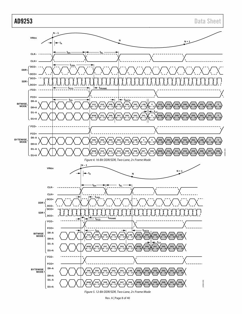
Figure 4. 16-Bit DDR/SDR, Two-Lane, 2× Frame Mode
1006
5-00
6
D0–A
D0+A
D1–A
D1+A
FCO–
BYTEWISEMODE
FCO+
D0–A
D0+A
D1–A
D1+A
FCO–
DCO–
CLK+
CLK–
DCO+
FCO+
BITWISEMODE
SDR
DDR
DCO–
DCO+
D10N – 16
D08N – 16
D06N – 16
D04N – 16
D02N – 16
LSBN – 16
D10N – 17
D08N – 17
D06N – 17
D04N – 17
D02N – 17
LSBN – 17
MSBN – 16
D09N – 16
D07N – 16
D05N – 16
D03N – 16
D01N – 16
MSBN – 17
D09N – 17
D07N – 17
D05N – 17
D03N – 17
D01N – 17
D05N – 16
D04N – 16
D03N – 16
D02N – 16
D01N – 16
LSBN – 16
D05N – 17
D04N – 17
D03N – 17
D02N – 17
D01N – 17
LSBN – 17
MSBN – 16
D10N – 16
D09N – 16
D08N – 16
D07N – 16
D06N – 16
MSBN – 17
D10N – 17
D09N – 17
D08N – 17
D07N – 17
D06N – 17
tEH
tCPD
tFRAMEtFCO
tPD tDATA
tLD
VIN±x
tA
N – 1
NN + 1
tEL
Figure 5. 12-Bit DDR/SDR, Two-Lane, 2× Frame Mode
Data Sheet AD9253
Rev. A | Page 9 of 40
1006
5-00
2D0–x
D0+x
FCO–
DCO+
CLK+
VIN±x
CLK–
DCO–
FCO+
D12N – 17
MSBN – 17
D11N – 17
D10N – 17
D9N – 17
D8N – 17
D7N – 17
D6N – 17
D5N – 17
D4N – 17
D3N – 17
D2N – 17
D1N – 17
LSBN – 17
0N – 17
0N – 17
MSBN – 16
D14N – 16
D13N – 16
tA
tDATA
tEH
tFCO tFRAME
tPD
tCPD
tEL
N – 1
N
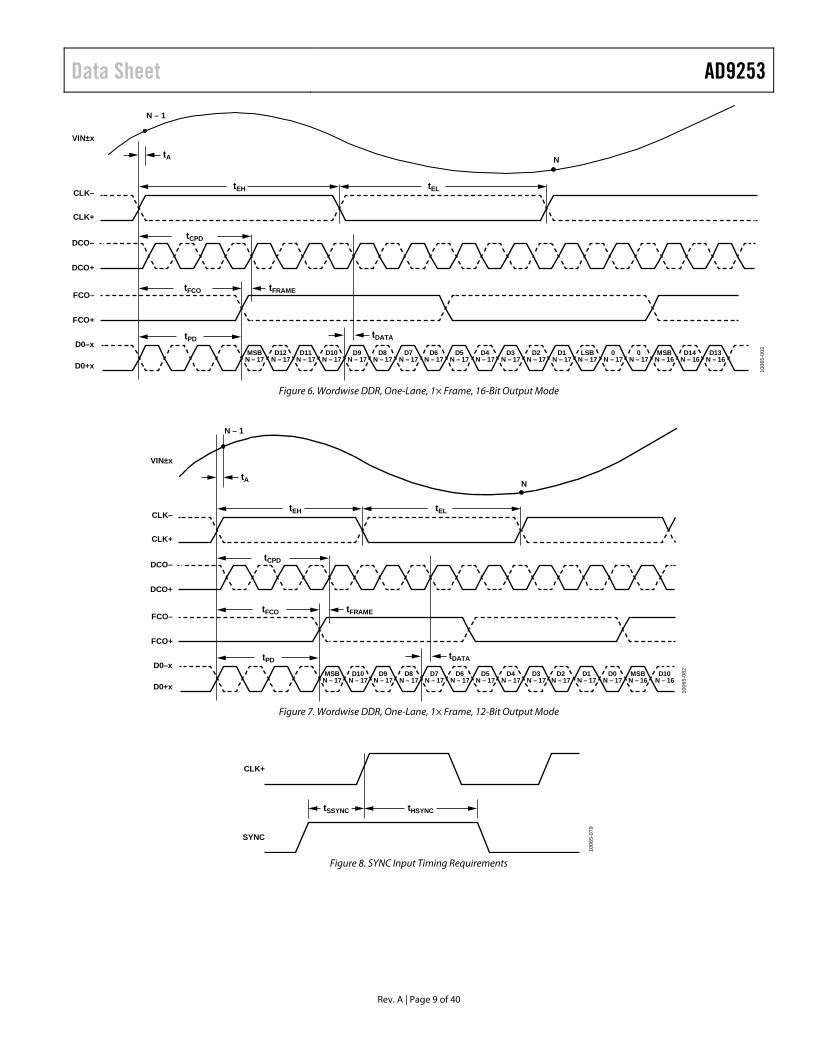
Figure 6. Wordwise DDR, One-Lane, 1× Frame, 16-Bit Output Mode
1006
5-08
2D0–x
D0+x
FCO–
DCO+
CLK+
VIN±x
CLK–
DCO–
FCO+
D10N – 17
MSBN – 17
D9N – 17
D8N – 17
D7N – 17
D6N – 17
D5N – 17
D4N – 17
D3N – 17
D2N – 17
D1N – 17
D0N – 17
MSBN – 16
D10N – 16
tA
tDATA
tEH
tFCO tFRAME
tPD
tCPD
tEL
N – 1
N
Figure 7. Wordwise DDR, One-Lane, 1× Frame, 12-Bit Output Mode
SYNC
CLK+
tHSYNCtSSYNC
1006
5-07
9
Figure 8. SYNC Input Timing Requirements
AD9253 Data Sheet
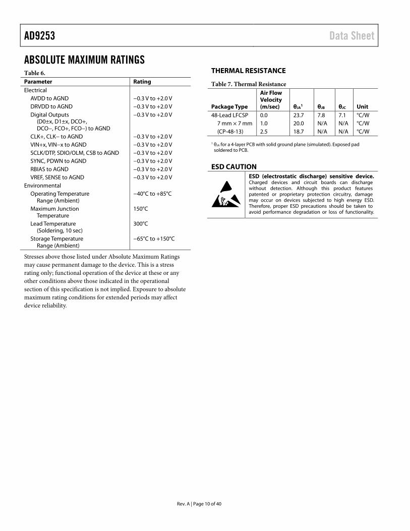
ABSOLUTE MAXIMUM RATINGS Table 6. Parameter Rating Electrical
AVDD to AGND −0.3 V to +2.0 V DRVDD to AGND −0.3 V to +2.0 V Digital Outputs
(D0±x, D1±x, DCO+, DCO−, FCO+, FCO−) to AGND
−0.3 V to +2.0 V
CLK+, CLK− to AGND −0.3 V to +2.0 V VIN+x, VIN−x to AGND −0.3 V to +2.0 V SCLK/DTP, SDIO/OLM, CSB to AGND −0.3 V to +2.0 V SYNC, PDWN to AGND −0.3 V to +2.0 V RBIAS to AGND −0.3 V to +2.0 V VREF, SENSE to AGND −0.3 V to +2.0 V
Environmental Operating Temperature
Range (Ambient) −40°C to +85°C
Maximum Junction Temperature
150°C
Lead Temperature (Soldering, 10 sec)
300°C
Storage Temperature Range (Ambient)
−65°C to +150°C
Stresses above those listed under Absolute Maximum Ratings may cause permanent damage to the device. This is a stress rating only; functional operation of the device at these or any other conditions above those indicated in the operational section of this specification is not implied. Exposure to absolute maximum rating conditions for extended periods may affect device reliability.
THERMAL RESISTANCE
Table 7. Thermal Resistance
Package Type
Air Flow Velocity (m/sec) θJA
1 θJB θJC Unit 48-Lead LFCSP 0.0 23.7 7.8 7.1 °C/W
7 mm × 7 mm 1.0 20.0 N/A N/A °C/W (CP-48-13) 2.5 18.7 N/A N/A °C/W
1 θJA for a 4-layer PCB with solid ground plane (simulated). Exposed pad
soldered to PCB.
ESD CAUTION
Rev. A | Page 10 of 40
Data Sheet AD9253
Rev. A | Page 11 of 40
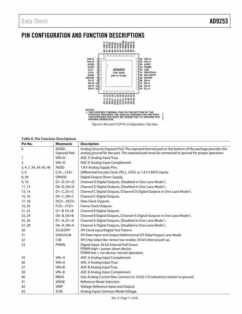
PIN CONFIGURATION AND FUNCTION DESCRIPTIONS
123
VIN+AVIN–AAVDD
4 PDWN5 CSB6 SDIO/OLM7 SCLK/DTP
24D
0+B
23D
0–B
22D
1+B
21D
1–B
20FC
O+
19FC
O–
18D
CO
+17
DC
O–
16D
0+C
15D
0–C
14D
1+C
13D
1–C
44SY
NC
45AV
DD
46AV
DD
47VI
N–C
48VI
N+C
43VC
M42
VREF
41SE
NSE
40R
BIA
S39
AVD
D38
VIN
–B37
VIN
+B
25D0+D26D0–D27D1+D28D1–D29DRVDD30AVDD31CLK+32CLK–33AVDD34AVDD35VIN–D36VIN+D
8 DRVDD9 D0+A
10 D0–A11 D1+A12 D1–A
1006
5-00
7
AD9253TOP VIEW
(Not to Scale)
NOTES1. THE EXPOSED THERMAL PAD ON THE BOTTOM OF THE
PACKAGE PROVIDES THE ANALOG GROUND FOR THE PART.THIS EXPOSED PAD MUST BE CONNECTED TO GROUND FORPROPER OPERATION.
Figure 9. 48-Lead LFCSP Pin Configuration, Top View
Table 8. Pin Function Descriptions Pin No. Mnemonic Description 0 AGND,
Exposed Pad Analog Ground, Exposed Pad. The exposed thermal pad on the bottom of the package provides the analog ground for the part. This exposed pad must be connected to ground for proper operation.
1 VIN+D ADC D Analog Input True. 2 VIN−D ADC D Analog Input Complement. 3, 4, 7, 34, 39, 45, 46 AVDD 1.8 V Analog Supply Pins. 5, 6 CLK−, CLK+ Differential Encode Clock. PECL, LVDS, or 1.8 V CMOS inputs. 8, 29 DRVDD Digital Output Driver Supply. 9, 10 D1−D, D1+D Channel D Digital Outputs, (Disabled in One-Lane Mode1). 11, 12 D0−D, D0+D Channel D Digital Outputs, (Disabled in One-Lane Mode1). 13, 14 D1−C, D1+C Channel C Digital Outputs, (Channel D Digital Outputs in One-Lane Mode1). 15, 16 D0−C, D0+C Channel C Digital Outputs. 17, 18 DCO−, DCO+ Data Clock Outputs. 19, 20 FCO−, FCO+ Frame Clock Outputs. 21, 22 D1−B, D1+B Channel B Digital Outputs. 23, 24 D0−B, D0+B Channel B Digital Outputs, (Channel A Digital Outputs in One-Lane Mode1). 25, 26 D1−A, D1+A Channel A Digital Outputs, (Disabled in One-Lane Mode1). 27, 28 D0−A, D0+A Channel A Digital Outputs, (Disabled in One-Lane Mode1). 30 SCLK/DTP SPI Clock Input/Digital Test Pattern. 31 SDIO/OLM SPI Data Input and Output Bidirectional SPI Data/Output Lane Mode. 32 CSB SPI Chip Select Bar. Active low enable; 30 kΩ internal pull-up. 33 PDWN Digital Input, 30 kΩ Internal Pull-Down.
PDWN high = power-down device. PDWN low = run device, normal operation.
35 VIN−A ADC A Analog Input Complement. 36 VIN+A ADC A Analog Input True. 37 VIN+B ADC B Analog Input True. 38 VIN−B ADC B Analog Input Complement. 40 RBIAS Sets Analog Current Bias. Connect to 10 kΩ (1% tolerance) resistor to ground. 41 SENSE Reference Mode Selection. 42 VREF Voltage Reference Input and Output. 43 VCM Analog Input Common-Mode Voltage.
AD9253 Data Sheet
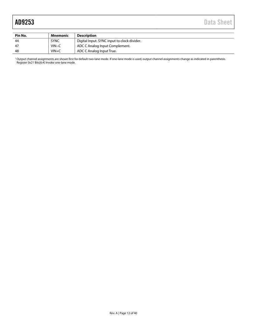
Pin No. Mnemonic Description 44 SYNC Digital Input. SYNC input to clock divider. 47 VIN−C ADC C Analog Input Complement. 48 VIN+C ADC C Analog Input True.
1 Output channel assignments are shown first for default two-lane mode. If one-lane mode is used, output channel assignments change as indicated in parenthesis. Register 0x21 Bits[6:4] invoke one-lane mode.
Rev. A | Page 12 of 40
Data Sheet AD9253
TYPICAL PERFORMANCE CHARACTERISTICS AD9253-80
0
–20
–40
–60
–80
–100
–120
–1400 105 15 20 25 30 4035
AM
PLIT
UD
E (d
BFS
)
FREQUENCY (MHz) 1006
5-01
6
AIN = –1dBFSSNR = 75.5dBENOB = 12.07BITSSFDR = 99.3dBc
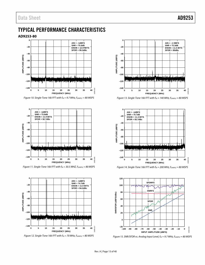
Figure 10. Single-Tone 16k FFT with fIN = 9.7 MHz, fSAMPLE = 80 MSPS
0
–20
–40
–60
–80
–100
–120
–1400 105 15 20 25 30 4035
AM
PLIT
UD
E (d
BFS
)
FREQUENCY (MHz) 1006
5-08
9
AIN = –1dBFSSNR = 73.9dBENOB = 11.9 BITSSFDR = 92.7dBc
Figure 11. Single-Tone 16k FFT with fIN = 30.5 MHZ, fSAMPLE = 80 MSPS
0
–20
–40
–60
–80
–100
–120
–1400 105 15 20 25 30 4035
AM
PLIT
UD
E (d
BFS
)
FREQUENCY (MHz) 1006
5-01
7
AIN = –1dBFSSNR = 74.7dBENOB = 11.9 BITSSFDR = 94.2dBc
Figure 12. Single-Tone 16k FFT with fIN = 70 MHz, fSAMPLE = 80 MSPS
105 15 20 25 30 4035
0
–20
–40
–60
–80
–100
–120
–1400
AM
PLIT
UD
E (d
BFS
)
FREQUENCY (MHz) 1006
5-01
8
AIN = –1 DBFSSNR = 72.3dBENOB = 11.5 BITSSFDR = 85dBc
Figure 13. Single-Tone 16k FFT with fIN = 140 MHz, fSAMPLE = 80 MSPS
0
–20
–40
–60
–80
–100
–120
–1400 105 15 20 25 30 4035
AM
PLIT
UD
E (d
BFS
)
FREQUENCY (MHz) 1006
5-01
9
AIN = –1dBFSSNR = 70.7dBENOB = 11.3 BITSSFDR = 83.7dBc
Figure 14. Single-Tone 16k FFT with fIN = 200 MHz, fSAMPLE = 80 MSPS
120
–20–100 0
SNR
/SFD
R (d
BFS
/dB
c)
INPUT AMPLITUDE (dBFS) 1006
5-03
0
SFDRFS
SFDR
SNRFS
SNR
0
20
40
60
80
100
–90 –80 –70 –60 –50 –40 –30 –20 –10
Figure 15. SNR/SFDR vs. Analog Input Level, fIN = 9.7 MHz, fSAMPLE = 80 MSPS
Rev. A | Page 13 of 40
AD9253 Data Sheet
0
–20
–40
–60
–80
–100
–120
–1400 105 15 20 25 30 4035
AM
PLIT
UD
E (d
BFS
)
FREQUENCY (MHz) 1006
5-03
3
AIN1 AND AIN2 = –7dBFSSFDR = 90.9dBcIMD2 = 91dBcIMD3 = 90.9dBc
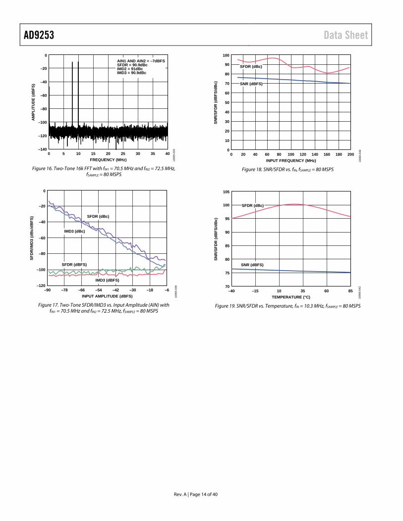
Figure 16. Two-Tone 16k FFT with fIN1 = 70.5 MHz and fIN2 = 72.5 MHz, fSAMPLE = 80 MSPS
0
–20
–40
–60
–80
–100
–120–90 –78 –66 –54 –42 –6–18–30
SFD
R/IM
D3
(dB
c/dB
FS)
INPUT AMPLITUDE (dBFS) 1006
5-03
6
SFDR (dBc)
SFDR (dBFS)
IMD3 (dBc)
IMD3 (dBFS)
Figure 17. Two-Tone SFDR/IMD3 vs. Input Amplitude (AIN) with fIN1 = 70.5 MHz and fIN2 = 72.5 MHz, fSAMPLE = 80 MSPS
100
00 200
SNR
/SFD
R (d
BFS
/dB
c)
INPUT FREQUENCY (MHz) 1006
5-03
9
70
10
20
30
40
50
60
80
90
100 120 1408020 40 60 180160
SFDR (dBc)
SNR (dBFS)
Figure 18. SNR/SFDR vs. fIN, fSAMPLE = 80 MSPS
105
70–40 85
SNR
/SFD
R (d
BFS
/dB
c)
TEMPERATURE (°C) 1006
5-04
2
75
80
85
90
95
100
–15 10 35 60
SFDR (dBc)
SNR (dBFS)
Figure 19. SNR/SFDR vs. Temperature, fIN = 10.3 MHz, fSAMPLE = 80 MSPS
Rev. A | Page 14 of 40
Data Sheet AD9253
AD9253-105 0
–20
–40
–60
–80
–100
–120
–1400 10 20 30 40 50
AM
PLIT
UD
E (d
BFS
)
FREQUENCY (MHz) 1006
5-02
0
AIN = –1dBFSSNR = 75.1dBENOB = 12.02 BITSSFDR = 97.8dBc
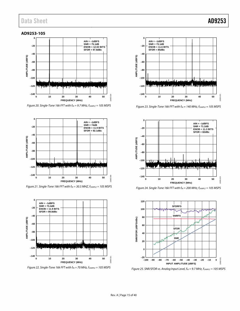
Figure 20. Single-Tone 16k FFT with fIN = 9.7 MHz, fSAMPLE = 105 MSPS
0
–20
–40
–60
–80
–100
–120
–1400 10 20 30 40 50
AM
PLIT
UD
E (d
BFS
)
FREQUENCY (MHz) 1006
5-09
0
AIN = –1dBFSSNR = 74dBENOB = 11.9 BITSSFDR = 92.1dBc
Figure 21. Single-Tone 16k FFT with fIN = 30.5 MHZ, fSAMPLE = 105 MSPS
0
–20
–40
–60
–80
–100
–120
–1400 10 20 30 40 50
AM
PLIT
UD
E (d
BFS
)
FREQUENCY (MHz) 1006
5-02
1
AIN = –1dBFSSNR = 73.4dBENOB = 11.9 BITSSFDR = 89.8dBc
Figure 22. Single-Tone 16k FFT with fIN = 70 MHz, fSAMPLE = 105 MSPS
0
–20
–40
–60
–80
–100
–120
–1400 10 20 30 40 50
AM
PLIT
UD
E (d
BFS
)
FREQUENCY (MHz) 1006
5-02
2
AIN = –1dBFSSNR = 73.1dBENOB = 11.6 BITSSFDR = 85dBc
Figure 23. Single-Tone 16k FFT with fIN = 140 MHz, fSAMPLE = 105 MSPS
0
–20
–40
–60
–80
–100
–120
–1400 10 20 30 40 50
AM
PLIT
UD
E (d
BFS
)
FREQUENCY (MHz) 1006
5-02
3
AIN = –1dBFSSNR = 71.2dBENOB = 11.3 BITSSFDR = 82dBc
Figure 24. Single-Tone 16k FFT with fIN = 200 MHz, fSAMPLE = 105 MSPS
120
–20–100 0
SNR
/SFD
R (d
BFS
/dB
c)
INPUT AMPLITUDE (dBFS) 1006
5-03
1
SFDRFS
SFDR
SNRFS
SNR
0
20
40
60
80
100
–90 –80 –70 –60 –50 –40 –30 –20 –10
Figure 25. SNR/SFDR vs. Analog Input Level, fIN = 9.7 MHz, fSAMPLE = 105 MSPS
Rev. A | Page 15 of 40
AD9253 Data Sheet
0
–20
–40
–60
–80
–100
–120
–1400 10 20 30 40 50
AM
PLIT
UD
E (d
BFS
)
FREQUENCY (MHz) 1006
5-03
4
AIN1 AND AIN2 = –7dBFSSFDR = 87.5dBcIMD2 = 92.6dBcIMD3 = 87.5dBc
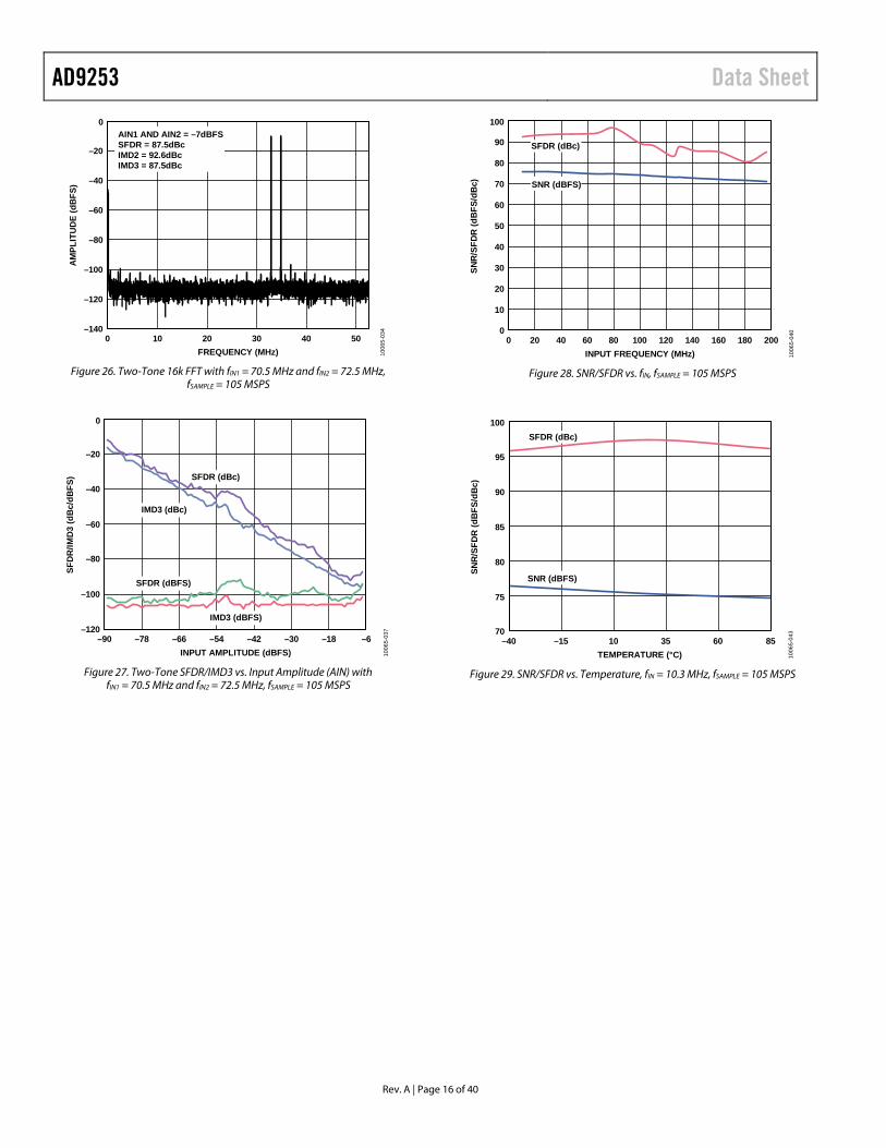
Figure 26. Two-Tone 16k FFT with fIN1 = 70.5 MHz and fIN2 = 72.5 MHz, fSAMPLE = 105 MSPS
0
–20
–40
–60
–80
–100
–120–90 –78 –66 –54 –42 –6–18–30
SFD
R/IM
D3
(dB
c/dB
FS)
INPUT AMPLITUDE (dBFS) 1006
5-03
7
SFDR (dBc)
SFDR (dBFS)
IMD3 (dBc)
IMD3 (dBFS)
Figure 27. Two-Tone SFDR/IMD3 vs. Input Amplitude (AIN) with fIN1 = 70.5 MHz and fIN2 = 72.5 MHz, fSAMPLE = 105 MSPS
SNR
/SFD
R (d
BFS
/dB
c)
INPUT FREQUENCY (MHz) 1006
5-04
0
SFDR (dBc)
SNR (dBFS)
100
00 200
70
10
20
30
40
50
60
80
90
100 120 1408020 40 60 180160
Figure 28. SNR/SFDR vs. fIN, fSAMPLE = 105 MSPS
100
70–40 85
SNR
/SFD
R (d
BFS
/dB
c)
TEMPERATURE (°C) 1006
5-04
3
75
80
85
90
95
–15 10 35 60
SFDR (dBc)
SNR (dBFS)
Figure 29. SNR/SFDR vs. Temperature, fIN = 10.3 MHz, fSAMPLE = 105 MSPS
Rev. A | Page 16 of 40
Data Sheet AD9253
AD9253-125
1006
5-02
4
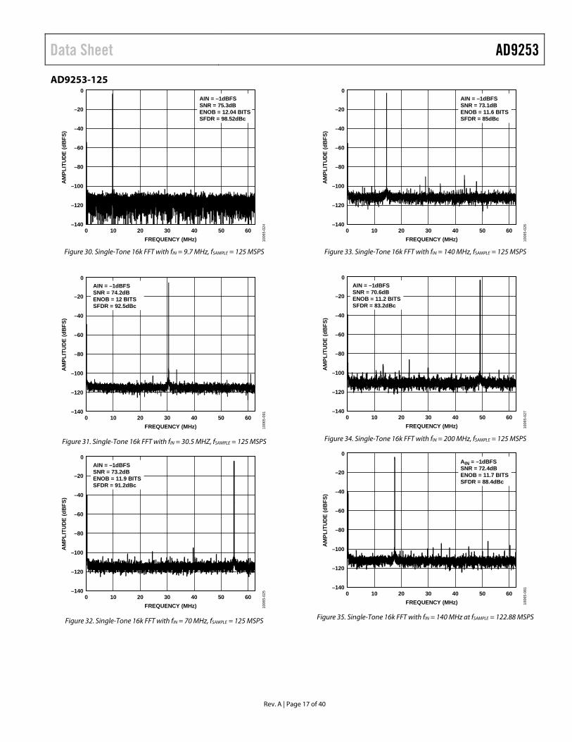
AIN = –1dBFSSNR = 75.3dBENOB = 12.04 BITSSFDR = 98.52dBc
0
–20
–40
–60
–80
–100
–120
–1400 10 20 30 40 50 60
AM
PLIT
UD
E (d
BFS
)
FREQUENCY (MHz)
Figure 30. Single-Tone 16k FFT with fIN = 9.7 MHz, fSAMPLE = 125 MSPS
0
–20
–40
–60
–80
–100
–120
–1400 10 20 30 40 50 60
AM
PLIT
UD
E (d
BFS
)
FREQUENCY (MHz) 1006
5-09
1
AIN = –1dBFSSNR = 74.2dBENOB = 12 BITSSFDR = 92.5dBc
Figure 31. Single-Tone 16k FFT with fIN = 30.5 MHZ, fSAMPLE = 125 MSPS
0
–20
–40
–60
–80
–100
–120
–1400 10 20 30 40 50 60
AM
PLIT
UD
E (d
BFS
)
FREQUENCY (MHz) 1006
5-02
5
AIN = –1dBFSSNR = 73.2dBENOB = 11.9 BITSSFDR = 91.2dBc
Figure 32. Single-Tone 16k FFT with fIN = 70 MHz, fSAMPLE = 125 MSPS
0
–20
–40
–60
–80
–100
–120
–1400 10 20 30 40 50 60
AM
PLIT
UD
E (d
BFS
)
FREQUENCY (MHz) 1006
5-02
6
AIN = –1dBFSSNR = 73.1dBENOB = 11.6 BITSSFDR = 85dBc
Figure 33. Single-Tone 16k FFT with fIN = 140 MHz, fSAMPLE = 125 MSPS
0
–20
–40
–60
–80
–100
–120
–1400 10 20 30 40 50 60
AM
PLIT
UD
E (d
BFS
)
FREQUENCY (MHz) 1006
5-02
7
AIN = –1dBFSSNR = 70.6dBENOB = 11.2 BITSSFDR = 83.2dBc
Figure 34. Single-Tone 16k FFT with fIN = 200 MHz, fSAMPLE = 125 MSPS
0
–20
–40
–60
–80
–100
–120
–1400 10 20 30 40 50 60
AM
PLIT
UD
E (d
BFS
)
FREQUENCY (MHz) 1006
5-08
1
AIN = –1dBFSSNR = 72.4dBENOB = 11.7 BITSSFDR = 88.4dBc
Figure 35. Single-Tone 16k FFT with fIN = 140 MHz at fSAMPLE = 122.88 MSPS
Rev. A | Page 17 of 40
AD9253 Data Sheet
120
0–100 0
SNR
/SFD
R (d
BFS
/dB
c)
INPUT AMPLITUDE (dBFS) 1006
5-03
2
SFDRFS
SFDR
SNRFS
SNR20
40
60
80
100
–90 –80 –70 –60 –50 –40 –30 –20 –10
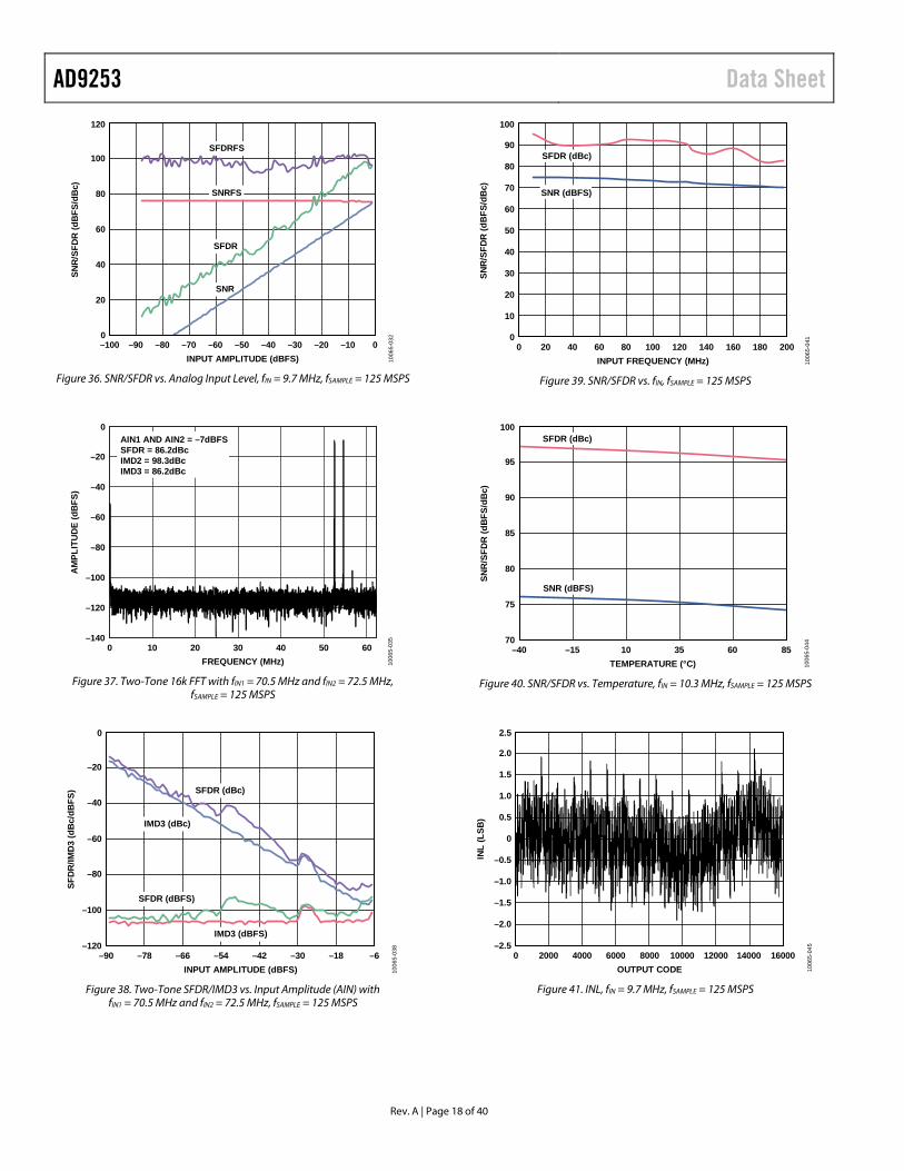
Figure 36. SNR/SFDR vs. Analog Input Level, fIN = 9.7 MHz, fSAMPLE = 125 MSPS
0
–20
–40
–60
–80
–100
–120
–1400 10 20 30 40 6050
AM
PLIT
UD
E (d
BFS
)
FREQUENCY (MHz) 1006
5-03
5
AIN1 AND AIN2 = –7dBFSSFDR = 86.2dBcIMD2 = 98.3dBcIMD3 = 86.2dBc
Figure 37. Two-Tone 16k FFT with fIN1 = 70.5 MHz and fIN2 = 72.5 MHz, fSAMPLE = 125 MSPS
0
–20
–40
–60
–80
–100
–120–90 –78 –66 –54 –42 –6–18–30
SFD
R/IM
D3
(dB
c/dB
FS)
INPUT AMPLITUDE (dBFS) 1006
5-03
8
SFDR (dBc)
SFDR (dBFS)
IMD3 (dBc)
IMD3 (dBFS)
Figure 38. Two-Tone SFDR/IMD3 vs. Input Amplitude (AIN) with fIN1 = 70.5 MHz and fIN2 = 72.5 MHz, fSAMPLE = 125 MSPS
SNR
/SFD
R (d
BFS
/dB
c)
INPUT FREQUENCY (MHz) 1006
5-04
1
100
00 200
70
10
20
30
40
50
60
80
90
100 120 1408020 40 60 180160
SNR (dBFS)
SFDR (dBc)
Figure 39. SNR/SFDR vs. fIN, fSAMPLE = 125 MSPS
100
70–40 85
SNR
/SFD
R (d
BFS
/dB
c)
TEMPERATURE (°C) 1006
5-04
4
75
80
85
90
95
–15 10 35 60
SFDR (dBc)
SNR (dBFS)
Figure 40. SNR/SFDR vs. Temperature, fIN = 10.3 MHz, fSAMPLE = 125 MSPS
2.5
–2.50 16000
INL
(LSB
)
OUTPUT CODE 1006
5-04
5
–2.0
–1.5
–1.0
–0.5
0
0.5
1.0
1.5
2.0
2000 4000 6000 8000 10000 12000 14000
Figure 41. INL, fIN = 9.7 MHz, fSAMPLE = 125 MSPS
Rev. A | Page 18 of 40
Data Sheet AD9253
1.0
–1.00 16000
DN
L (L
SB)
OUTPUT CODE 1006
5-04
6
–0.8
–0.6
–0.4
–0.2
0
0.2
0.4
0.6
0.8
2000 4000 6000 8000 10000 12000 14000
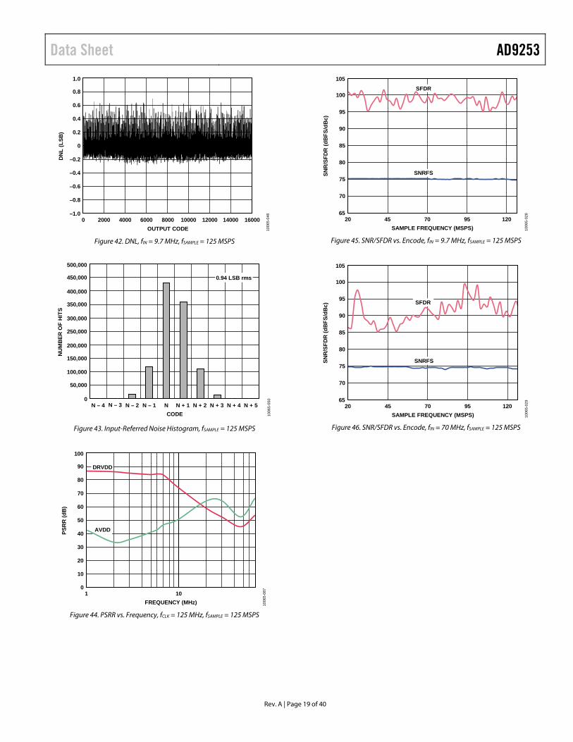
Figure 42. DNL, fIN = 9.7 MHz, fSAMPLE = 125 MSPS
500,000
450,000
400,000
350,000
300,000
250,000
200,000
0
50,000
100,000
150,000
N – 4 N – 3 N – 2 N – 1 N + 1 N + 2 N + 3 N + 4 N + 5N
NU
MB
ER O
F H
ITS
CODE 1006
5-05
0
0.94 LSB rms
Figure 43. Input-Referred Noise Histogram, fSAMPLE = 125 MSPS
100
01 10
PSR
R (d
B)
FREQUENCY (MHz) 1006
5-08
7
10
20
30
40
50
60
70
80
90
AVDD
DRVDD
Figure 44. PSRR vs. Frequency, fCLK = 125 MHz, fSAMPLE = 125 MSPS
105
6520 45 70 95 120
SNR
/SFD
R (d
BFS
/dB
c)
SAMPLE FREQUENCY (MSPS) 1006
5-02
8
70
75
80
85
90
95
100SFDR
SNRFS
Figure 45. SNR/SFDR vs. Encode, fIN = 9.7 MHz, fSAMPLE = 125 MSPS
105
6520 45 70 95 120
SNR
/SFD
R (d
BFS
/dB
c)
SAMPLE FREQUENCY (MSPS) 1006
5-02
9
70
75
80
85
90
95
100
SNRFS
SFDR
Figure 46. SNR/SFDR vs. Encode, fIN = 70 MHz, fSAMPLE = 125 MSPS
Rev. A | Page 19 of 40
AD9253 Data Sheet
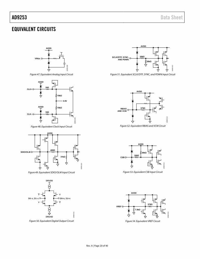
EQUIVALENT CIRCUITS
AVDD
VIN±x
1006
5-00
8
Figure 47. Equivalent Analog Input Circuit 10
065-
009
CLK+
CLK–
0.9V
15kΩ
10Ω
10Ω
15kΩAVDD
AVDD
Figure 48. Equivalent Clock Input Circuit
1006
5-01
0
31kΩ
SDIO/OLM400Ω
AVDD
Figure 49. Equivalent SDIO/OLM Input Circuit
DRVDD
DRGND
D0–x, D1–x D0+x, D1+x
V
V
V
V
1006
5-01
1
Figure 50. Equivalent Digital Output Circuit
350Ω
AVDD
30kΩ
SCLK/DTP, SYNC,AND PDWN
1006
5-01
2
Figure 51. Equivalent SCLK/DTP, SYNC, and PDWN Input Circuit
RBIASAND VCM
375Ω
AVDD
1006
5-01
3
Figure 52. Equivalent RBIAS and VCM Circuit
CSB350Ω
AVDD
30kΩ
1006
5-01
4
Figure 53. Equivalent CSB Input Circuit
VREF
1006
5-01
5
AVDD
7.5kΩ
375Ω
Figure 54. Equivalent VREF Circuit
Rev. A | Page 20 of 40
Data Sheet AD9253
THEORY OF OPERATION The AD9253 is a multistage, pipelined ADC. Each stage provides sufficient overlap to correct for flash errors in the preceding stage. The quantized outputs from each stage are combined into a final 14-bit result in the digital correction logic. The serializer transmits this converted data in a 16-bit output. The pipelined architecture permits the first stage to operate with a new input sample while the remaining stages operate with preceding samples. Sampling occurs on the rising edge of the clock.
Each stage of the pipeline, excluding the last, consists of a low resolution flash ADC connected to a switched-capacitor DAC and an interstage residue amplifier (for example, a multiplying digital-to-analog converter (MDAC)). The residue amplifier magnifies the difference between the reconstructed DAC output and the flash input for the next stage in the pipeline. One bit of redundancy is used in each stage to facilitate digital correction of flash errors. The last stage simply consists of a flash ADC.
The output staging block aligns the data, corrects errors, and passes the data to the output buffers. The data is then serialized and aligned to the frame and data clocks.
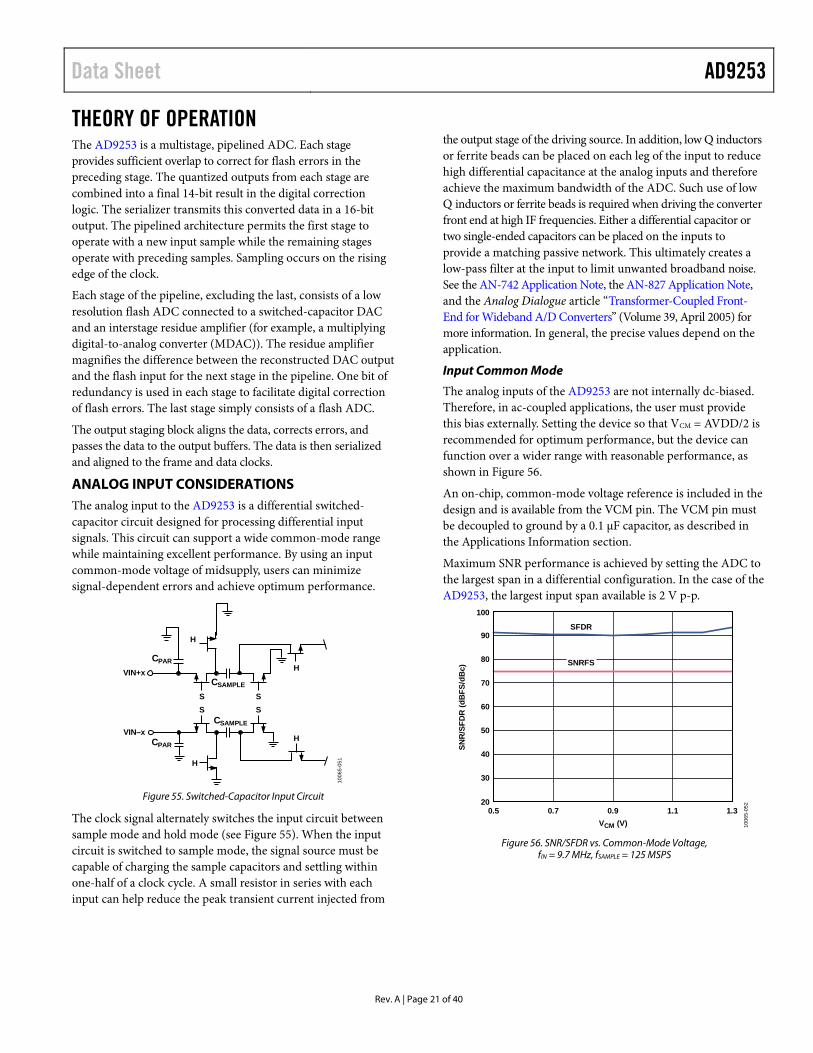
ANALOG INPUT CONSIDERATIONS The analog input to the AD9253 is a differential switched-capacitor circuit designed for processing differential input signals. This circuit can support a wide common-mode range while maintaining excellent performance. By using an input common-mode voltage of midsupply, users can minimize signal-dependent errors and achieve optimum performance.
S S
HCPAR
CSAMPLE
CSAMPLE
CPAR
VIN–x
H
S S
HVIN+x
H
1006
5-05
1
Figure 55. Switched-Capacitor Input Circuit
The clock signal alternately switches the input circuit between sample mode and hold mode (see Figure 55). When the input circuit is switched to sample mode, the signal source must be capable of charging the sample capacitors and settling within one-half of a clock cycle. A small resistor in series with each input can help reduce the peak transient current injected from
the output stage of the driving source. In addition, low Q inductors or ferrite beads can be placed on each leg of the input to reduce high differential capacitance at the analog inputs and therefore achieve the maximum bandwidth of the ADC. Such use of low Q inductors or ferrite beads is required when driving the converter front end at high IF frequencies. Either a differential capacitor or two single-ended capacitors can be placed on the inputs to provide a matching passive network. This ultimately creates a low-pass filter at the input to limit unwanted broadband noise. See the AN-742 Application Note, the AN-827 Application Note, and the Analog Dialogue article “Transformer-Coupled Front-End for Wideband A/D Converters” (Volume 39, April 2005) for more information. In general, the precise values depend on the application.
Input Common Mode
The analog inputs of the AD9253 are not internally dc-biased. Therefore, in ac-coupled applications, the user must provide this bias externally. Setting the device so that VCM = AVDD/2 is recommended for optimum performance, but the device can function over a wider range with reasonable performance, as shown in Figure 56.
An on-chip, common-mode voltage reference is included in the design and is available from the VCM pin. The VCM pin must be decoupled to ground by a 0.1 µF capacitor, as described in the Applications Information section.
Maximum SNR performance is achieved by setting the ADC to the largest span in a differential configuration. In the case of the AD9253, the largest input span available is 2 V p-p.
100
200.5
SNR
/SFD
R (d
BFS
/dB
c)
VCM (V) 1006
5-05
2
30
40
50
60
70
80
90
0.7 0.9 1.1 1.3
SNRFS
SFDR
Figure 56. SNR/SFDR vs. Common-Mode Voltage,
fIN = 9.7 MHz, fSAMPLE = 125 MSPS
Rev. A | Page 21 of 40
AD9253 Data Sheet
Rev. A | Page 22 of 40
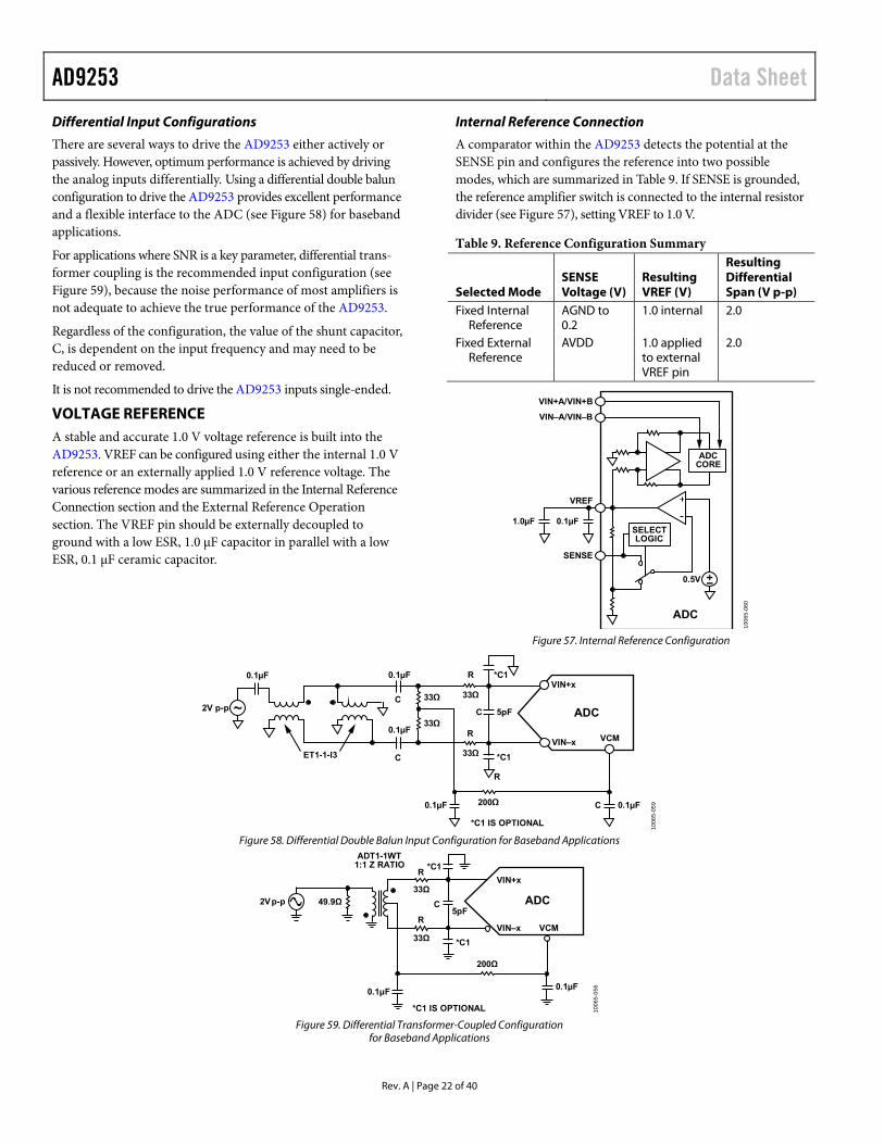
Differential Input Configurations
There are several ways to drive the AD9253 either actively or passively. However, optimum performance is achieved by driving the analog inputs differentially. Using a differential double balun configuration to drive the AD9253 provides excellent performance and a flexible interface to the ADC (see Figure 58) for baseband applications.
For applications where SNR is a key parameter, differential trans-former coupling is the recommended input configuration (see Figure 59), because the noise performance of most amplifiers is not adequate to achieve the true performance of the AD9253.
Regardless of the configuration, the value of the shunt capacitor, C, is dependent on the input frequency and may need to be reduced or removed.
It is not recommended to drive the AD9253 inputs single-ended.
VOLTAGE REFERENCE A stable and accurate 1.0 V voltage reference is built into the AD9253. VREF can be configured using either the internal 1.0 V reference or an externally applied 1.0 V reference voltage. The various reference modes are summarized in the Internal Reference Connection section and the External Reference Operation section. The VREF pin should be externally decoupled to ground with a low ESR, 1.0 μF capacitor in parallel with a low ESR, 0.1 μF ceramic capacitor.
Internal Reference Connection
A comparator within the AD9253 detects the potential at the SENSE pin and configures the reference into two possible modes, which are summarized in Table 9. If SENSE is grounded, the reference amplifier switch is connected to the internal resistor divider (see Figure 57), setting VREF to 1.0 V.
Table 9. Reference Configuration Summary
Selected Mode SENSE Voltage (V)
Resulting VREF (V)
Resulting Differential Span (V p-p)
Fixed Internal Reference
AGND to 0.2
1.0 internal 2.0
Fixed External Reference
AVDD 1.0 applied to external VREF pin
2.0
VREF
SENSE
0.5V
ADC
SELECTLOGIC
0.1µF1.0µF
VIN–A/VIN–B
VIN+A/VIN+B
ADCCORE
1006
5-06
0
Figure 57. Internal Reference Configuration
ADC
R0.1µF0.1µF
2V p-p
VCM
C
*C1
*C1
C
R0.1µF
0.1µF 0.1µF
33Ω
200Ω
33Ω 33Ω
33Ω
VIN+x
VIN–x
1006
5-05
9
ET1-1-I3 C
C
5pF
R
*C1 IS OPTIONAL Figure 58. Differential Double Balun Input Configuration for Baseband Applications
2Vp-p
R
R
*C1
*C1 IS OPTIONAL
49.9Ω
0.1μF
ADT1-1WT1:1 Z RATIO
VIN–x
ADC
VIN+x
*C1
C
VCM
1006
5-05
6
33Ω
33Ω
200Ω
0.1µF
5pF
Figure 59. Differential Transformer-Coupled Configuration
for Baseband Applications
Data Sheet AD9253 If the internal reference of the AD9253 is used to drive multiple converters to improve gain matching, the loading of the reference by the other converters must be considered. Figure 60 shows how the internal reference voltage is affected by loading.
0
–0.5
–1.0
–1.5
–2.0
–2.5
–3.0
–3.5
–4.0
–4.5
–5.00 3.02.52.01.51.00.5
V REF
ER
RO
R (%
)
LOAD CURRENT (mA) 1006
5-06
1
INTERNAL VREF = 1V
Figure 60. VREF Error vs. Load Current
External Reference Operation
The use of an external reference may be necessary to enhance the gain accuracy of the ADC or improve thermal drift charac-teristics. Figure 61 shows the typical drift characteristics of the internal reference in 1.0 V mode.
4
–8–40 85
V REF
ER
RO
R (m
V)
TEMPERATURE (°C) 1006
5-06
2
–6
–4
–2
0
2
–15 10 35 60
Figure 61. Typical VREF Drift
When the SENSE pin is tied to AVDD, the internal reference is disabled, allowing the use of an external reference. An internal reference buffer loads the external reference with an equivalent 7.5 kΩ load (see Figure 54). The internal buffer generates the positive and negative full-scale references for the ADC core. There-fore, the external reference must be limited to a maximum of 1.0 V.
It is not recommended to leave the SENSE pin floating.
CLOCK INPUT CONSIDERATIONS For optimum performance, clock the AD9253 sample clock inputs, CLK+ and CLK−, with a differential signal. The signal is typically ac-coupled into the CLK+ and CLK− pins via a transformer or capacitors. These pins are biased internally (see Figure 48) and require no external bias.
Clock Input Options
The AD9253 has a flexible clock input structure. The clock input can be a CMOS, LVDS, LVPECL, or sine wave signal. Regardless of the type of signal being used, clock source jitter is of the most concern, as described in the Jitter Considerations section.
Figure 62 and Figure 63 show two preferred methods for clock-ing the AD9253 (at clock rates up to 1 GHz prior to internal CLK divider). A low jitter clock source is converted from a single-ended signal to a differential signal using either an RF transformer or an RF balun.
The RF balun configuration is recommended for clock frequencies between 125 MHz and 1 GHz, and the RF transformer is recom-mended for clock frequencies from 10 MHz to 200 MHz. The antiparallel Schottky diodes across the transformer/balun secondary winding limit clock excursions into the AD9253 to approximately 0.8 V p-p differential.
This limit helps prevent the large voltage swings of the clock from feeding through to other portions of the AD9253 while preserving the fast rise and fall times of the signal that are critical to achieving low jitter performance. However, the diode capacitance comes into play at frequencies above 500 MHz. Care must be taken in choosing the appropriate signal limiting diode.
0.1µF
0.1µF
0.1µF0.1µF
SCHOTTKYDIODES:
HSMS2822
CLOCKINPUT
50Ω 100Ω
CLK–
CLK+
ADC
Mini-Circuits®ADT1-1WT, 1:1 Z
XFMR
1006
5-06
4
Figure 62. Transformer-Coupled Differential Clock (Up to 200 MHz)
0.1µF
0.1µF0.1µFCLOCKINPUT
0.1µF
50Ω
CLK–
CLK+
SCHOTTKYDIODES:
HSMS2822
ADC
1006
5-06
5
Figure 63. Balun-Coupled Differential Clock (Up to 1 GHz)
If a low jitter clock source is not available, another option is to ac couple a differential PECL signal to the sample clock input pins, as shown in Figure 65. The AD9510/AD9511/AD9512/ AD9513/AD9514/AD9515/AD9516/AD9517 clock drivers offer excellent jitter performance.
A third option is to ac couple a differential LVDS signal to the sample clock input pins, as shown in Figure 66. The AD9510/ AD9511/AD9512/AD9513/AD9514/AD9515/AD9516/AD9517 clock drivers offer excellent jitter performance.
In some applications, it may be acceptable to drive the sample clock inputs with a single-ended 1.8 V CMOS signal. In such applications, drive the CLK+ pin directly from a CMOS gate, and
Rev. A | Page 23 of 40

AD9253 Data Sheet bypass the CLK− pin to ground with a 0.1 μF capacitor (see Figure 67).
Input Clock Divider
The AD9253 contains an input clock divider with the ability to divide the input clock by integer values between 1 and 8.
The AD9253 clock divider can be synchronized using the external SYNC input. Bit 0 and Bit 1 of Register 0x109 allow the clock divider to be resynchronized on every SYNC signal or only on the first SYNC signal after the register is written. A valid SYNC causes the clock divider to reset to its initial state. This synchronization feature allows multiple parts to have their clock dividers aligned to guarantee simultaneous input sampling.
Clock Duty Cycle
Typical high speed ADCs use both clock edges to generate a vari-ety of internal timing signals and, as a result, may be sensitive to clock duty cycle. Commonly, a ±5% tolerance is required on the clock duty cycle to maintain dynamic performance characteristics.
The AD9253 contains a duty cycle stabilizer (DCS) that retimes the nonsampling (falling) edge, providing an internal clock signal with a nominal 50% duty cycle. This allows the user to provide a wide range of clock input duty cycles without affecting the performance of the AD9253. Noise and distortion perform-ance are nearly flat for a wide range of duty cycles with the DCS on, as shown in Figure 64.
80
5540 60
SNR
FS (d
BFS
)
DUTY CYCLE (%) 1006
5-06
9
60
65
70
75
42 44 46 48 50 52 54 56 58
SNRFS (DCS OFF)
SNRFS (DCS ON)
Figure 64. SNR vs. DCS On/Off
Jitter in the rising edge of the input is still of concern and is not easily reduced by the internal stabilization circuit. The duty cycle control loop does not function for clock rates less than 20 MHz, nominally. The loop has a time constant associated with it that must be considered in applications in which the clock rate can change dynamically. A wait time of 1.5 µs to 5 µs is required after a dynamic clock frequency increase or decrease before the DCS loop is relocked to the input signal.
100Ω0.1µF
0.1µF0.1µF
0.1µF
240Ω240Ω50kΩ 50kΩCLK–
CLK+CLOCKINPUT
CLOCKINPUT
ADCAD951xPECL DRIVER
1006
5-06
6
Figure 65. Differential PECL Sample Clock (Up to 1 GHz)
100Ω0.1µF
0.1µF0.1µF
0.1µF
50kΩ 50kΩCLK–
CLK+
ADC
CLOCKINPUT
CLOCKINPUT
AD951xLVDS DRIVER
1006
5-06
7
Figure 66. Differential LVDS Sample Clock (Up to 1 GHz)
OPTIONAL100Ω 0.1µF
0.1µF
0.1µF
50Ω1
150Ω RESISTOR IS OPTIONAL.
CLK–
CLK+
ADC
VCC
1kΩ
1kΩ
CLOCKINPUT
AD951xCMOS DRIVER
1006
5-06
8
Figure 67. Single-Ended 1.8 V CMOS Input Clock (Up to 200 MHz)
Rev. A | Page 24 of 40
Data Sheet AD9253 Jitter Considerations
High speed, high resolution ADCs are sensitive to the quality of the clock input. The degradation in SNR at a given input frequency (fA) due only to aperture jitter (tJ) can be calculated by
SNR Degradation = 20 log10
×× JA tfπ21
In this equation, the rms aperture jitter represents the root sum square of all jitter sources, including the clock input, analog input signal, and ADC aperture jitter specifications. IF undersampling applications are particularly sensitive to jitter (see Figure 68).
The clock input should be treated as an analog signal in cases where aperture jitter may affect the dynamic range of the AD9253. Power supplies for clock drivers should be separated from the ADC output driver supplies to avoid modulating the clock signal with digital noise. Low jitter, crystal-controlled oscillators make the best clock sources. If the clock is generated from another type of source (by gating, dividing, or other methods), it should be retimed by the original clock at the last step.
Refer to the AN-501 Application Note and the AN-756 Application Note for more in-depth information about jitter performance as it relates to ADCs.
1 10 100 1000
16 BITS
14 BITS
12 BITS
30
40
50
60
70
80
90
100
110
120
130
0.125ps0.25ps
0.5ps1.0ps2.0ps
ANALOG INPUT FREQUENCY (MHz)
10 BITS
8 BITS
RMS CLOCK JITTER REQUIREMENT
SNR
(dB
)
1006
5-07
0
Figure 68. Ideal SNR vs. Input Frequency and Jitter
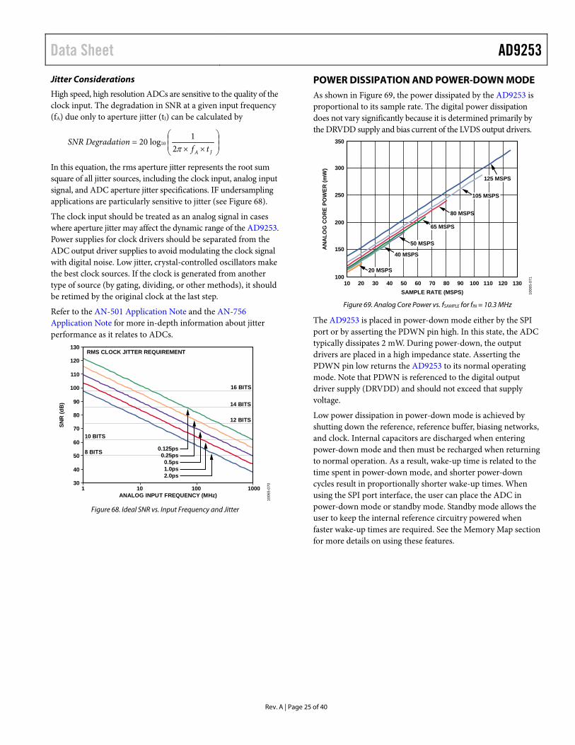
POWER DISSIPATION AND POWER-DOWN MODE As shown in Figure 69, the power dissipated by the AD9253 is proportional to its sample rate. The digital power dissipation does not vary significantly because it is determined primarily by the DRVDD supply and bias current of the LVDS output drivers.
350
300
250
200
150
10010 130
AN
ALO
G C
OR
E PO
WER
(mW
)
SAMPLE RATE (MSPS) 1006
5-07
1
20 30 40 50 60 70 80 90 100 110 120
50 MSPS
80 MSPS
125 MSPS
40 MSPS
20 MSPS
65 MSPS
105 MSPS
Figure 69. Analog Core Power vs. fSAMPLE for fIN = 10.3 MHz
The AD9253 is placed in power-down mode either by the SPI port or by asserting the PDWN pin high. In this state, the ADC typically dissipates 2 mW. During power-down, the output drivers are placed in a high impedance state. Asserting the PDWN pin low returns the AD9253 to its normal operating mode. Note that PDWN is referenced to the digital output driver supply (DRVDD) and should not exceed that supply voltage.
Low power dissipation in power-down mode is achieved by shutting down the reference, reference buffer, biasing networks, and clock. Internal capacitors are discharged when entering power-down mode and then must be recharged when returning to normal operation. As a result, wake-up time is related to the time spent in power-down mode, and shorter power-down cycles result in proportionally shorter wake-up times. When using the SPI port interface, the user can place the ADC in power-down mode or standby mode. Standby mode allows the user to keep the internal reference circuitry powered when faster wake-up times are required. See the Memory Map section for more details on using these features.
Rev. A | Page 25 of 40
AD9253 Data Sheet
DIGITAL OUTPUTS AND TIMING The AD9253 differential outputs conform to the ANSI-644 LVDS standard on default power-up. This can be changed to a low power, reduced signal option (similar to the IEEE 1596.3 standard) via the SPI. The LVDS driver current is derived on chip and sets the output current at each output equal to a nominal 3.5 mA. A 100 Ω differential termination resistor placed at the LVDS receiver inputs results in a nominal 350 mV swing (or 700 mV p-p differential) at the receiver.
When operating in reduced range mode, the output current is reduced to 2 mA. This results in a 200 mV swing (or 400 mV p-p differential) across a 100 Ω termination at the receiver.
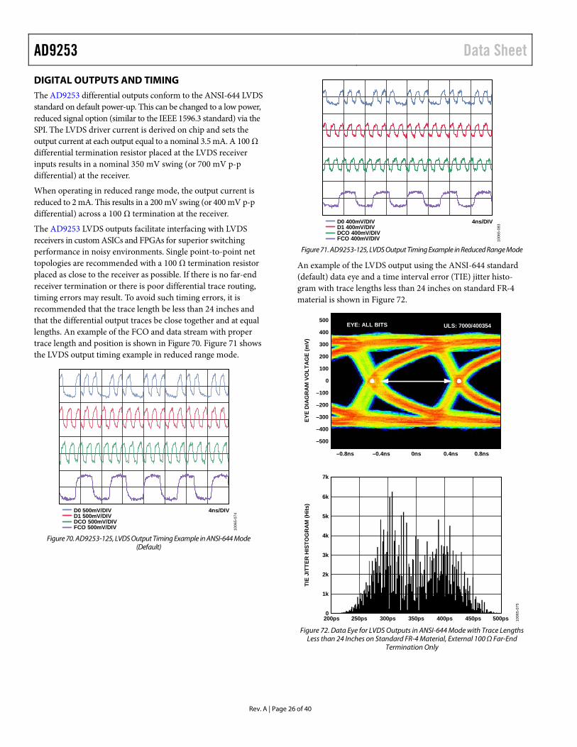
The AD9253 LVDS outputs facilitate interfacing with LVDS receivers in custom ASICs and FPGAs for superior switching performance in noisy environments. Single point-to-point net topologies are recommended with a 100 Ω termination resistor placed as close to the receiver as possible. If there is no far-end receiver termination or there is poor differential trace routing, timing errors may result. To avoid such timing errors, it is recommended that the trace length be less than 24 inches and that the differential output traces be close together and at equal lengths. An example of the FCO and data stream with proper trace length and position is shown in Figure 70. Figure 71 shows the LVDS output timing example in reduced range mode.
1006
5-07
4D0 500mV/DIVD1 500mV/DIVDCO 500mV/DIVFCO 500mV/DIV
4ns/DIV
Figure 70. AD9253-125, LVDS Output Timing Example in ANSI-644 Mode
(Default)
1006
5-08
3D0 400mV/DIVD1 400mV/DIVDCO 400mV/DIVFCO 400mV/DIV
4ns/DIV
Figure 71. AD9253-125, LVDS Output Timing Example in Reduced Range Mode
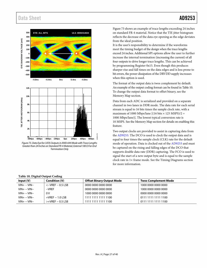
An example of the LVDS output using the ANSI-644 standard (default) data eye and a time interval error (TIE) jitter histo-gram with trace lengths less than 24 inches on standard FR-4 material is shown in Figure 72.
6k
7k
1k
2k
3k
5k
4k
0200ps 250ps 300ps 350ps 400ps 450ps 500ps
TIE
JITT
ER H
ISTO
GR
AM
(Hits
)
500
400
300
200
100
–500
–400
–300
–200
–100
0
–0.8ns –0.4ns 0ns 0.4ns 0.8ns
EYE
DIA
GR
AM
VO
LTA
GE
(mV)
EYE: ALL BITS ULS: 7000/400354
1006
5-07
5
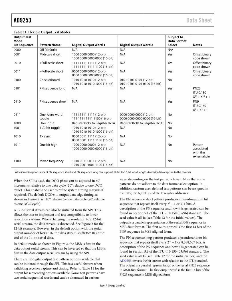
Figure 72. Data Eye for LVDS Outputs in ANSI-644 Mode with Trace Lengths
Less than 24 Inches on Standard FR-4 Material, External 100 Ω Far-End Termination Only
Rev. A | Page 26 of 40
Data Sheet AD9253
500
400
300
200
100
–500
–400
–300
–200
–100
0
–0.8ns –0.4ns 0ns 0.4ns –0.8ns
EYE
DIA
GR
AM
VO
LTA
GE
(mV)
EYE: ALL BITS ULS: 8000/414024
10k
12k
2k
4k
6k
8k
0k–800ps –600ps –400ps –200ps 0ps 200ps 400ps 600ps
TIE
JITT
ER H
ISTO
GR
AM
(Hits
)
1006
5-07
6
Figure 73. Data Eye for LVDS Outputs in ANSI-644 Mode with Trace Lengths Greater than 24 Inches on Standard FR-4 Material, External 100 Ω Far-End
Termination Only
Figure 73 shows an example of trace lengths exceeding 24 inches on standard FR-4 material. Notice that the TIE jitter histogram reflects the decrease of the data eye opening as the edge deviates from the ideal position. It is the user’s responsibility to determine if the waveforms meet the timing budget of the design when the trace lengths exceed 24 inches. Additional SPI options allow the user to further increase the internal termination (increasing the current) of all four outputs to drive longer trace lengths. This can be achieved by programming Register 0x15. Even though this produces sharper rise and fall times on the data edges and is less prone to bit errors, the power dissipation of the DRVDD supply increases when this option is used.
The format of the output data is twos complement by default. An example of the output coding format can be found in Table 10. To change the output data format to offset binary, see the Memory Map section.
Data from each ADC is serialized and provided on a separate channel in two lanes in DDR mode. The data rate for each serial stream is equal to 16 bits times the sample clock rate, with a maximum of 1000 Mbps/lane [(16 bits × 125 MSPS)/2 = 1000 Mbps/lane)]. The lowest typical conversion rate is 10 MSPS. See the Memory Map section for details on enabling this feature.
Two output clocks are provided to assist in capturing data from the AD9253. The DCO is used to clock the output data and is equal to four times the sample clock (CLK) rate for the default mode of operation. Data is clocked out of the AD9253 and must be captured on the rising and falling edges of the DCO that supports double data rate (DDR) capturing. The FCO is used to signal the start of a new output byte and is equal to the sample clock rate in 1× frame mode. See the Timing Diagrams section for more information.
Table 10. Digital Output Coding Input (V) Condition (V) Offset Binary Output Mode Twos Complement Mode VIN+ − VIN− <−VREF − 0.5 LSB 0000 0000 0000 0000 1000 0000 0000 0000 VIN+ − VIN− −VREF 0000 0000 0000 0000 1000 0000 0000 0000 VIN+ − VIN− 0 V 1000 0000 0000 0000 0000 0000 0000 0000 VIN+ − VIN− +VREF − 1.0 LSB 1111 1111 1111 1100 0111 1111 1111 1100 VIN+ − VIN− >+VREF − 0.5 LSB 1111 1111 1111 1100 0111 1111 1111 1100
Rev. A | Page 27 of 40
AD9253 Data Sheet Table 11. Flexible Output Test Modes Output Test Mode Bit Sequence Pattern Name Digital Output Word 1 Digital Output Word 2
Subject to Data Format Select Notes
0000 Off (default) N/A N/A N/A 0001 Midscale short 1000 0000 0000 (12-bit)
1000 0000 0000 0000 (16-bit) N/A Yes Offset binary
code shown 0010 +Full-scale short 1111 1111 1111 (12-bit)
1111 1111 1111 1100 (16-bit) N/A Yes Offset binary
code shown 0011 −Full-scale short 0000 0000 0000 (12-bit)
0000 0000 0000 0000 (16-bit) N/A Yes Offset binary
code shown 0100 Checkerboard 1010 1010 1010 (12-bit)
1010 1010 1010 1000 (16-bit) 0101 0101 0101 (12-bit) 0101 0101 0101 0100 (16-bit)
No
0101 PN sequence long1 N/A N/A Yes PN23 ITU 0.150 X23 + X18 + 1
0110 PN sequence short1 N/A N/A Yes PN9 ITU 0.150 X9 + X5 + 1
0111 One-/zero-word toggle
1111 1111 1111 (12-bit) 111 1111 1111 1100 (16-bit)
0000 0000 0000 (12-bit) 0000 0000 0000 0000 (16-bit)
No
1000 User input Register 0x19 to Register 0x1A Register 0x1B to Register 0x1C No 1001 1-/0-bit toggle 1010 1010 1010 (12-bit)
1010 1010 1010 1000 (16-bit) N/A No
1010 1× sync 0000 0011 1111 (12-bit) 0000 0001 1111 1100 (16-bit)
N/A No
1011 One bit high 1000 0000 0000 (12-bit) 1000 0000 0000 0000 (16-bit)
N/A No Pattern associated with the external pin
1100 Mixed frequency 1010 0011 0011 (12-bit) 1010 0001 1001 1100 (16-bit)
N/A No
1 All test mode options except PN sequence short and PN sequence long can support 12-bit to 16-bit word lengths to verify data capture to the receiver.
When the SPI is used, the DCO phase can be adjusted in 60° increments relative to one data cycle (30° relative to one DCO cycle). This enables the user to refine system timing margins if required. The default DCO± to output data edge timing, as shown in Figure 2, is 180° relative to one data cycle (90° relative to one DCO cycle).
A 12-bit serial stream can also be initiated from the SPI. This allows the user to implement and test compatibility to lower resolution systems. When changing the resolution to a 12-bit serial stream, the data stream is shortened. See Figure 3 for the 12-bit example. However, in the default option with the serial output number of bits at 16, the data stream stuffs two 0s at the end of the 14-bit serial data.
In default mode, as shown in Figure 2, the MSB is first in the data output serial stream. This can be inverted so that the LSB is first in the data output serial stream by using the SPI.
There are 12 digital output test pattern options available that can be initiated through the SPI. This is a useful feature when validating receiver capture and timing. Refer to Table 11 for the output bit sequencing options available. Some test patterns have two serial sequential words and can be alternated in various
ways, depending on the test pattern chosen. Note that some patterns do not adhere to the data format select option. In addition, custom user-defined test patterns can be assigned in the 0x19, 0x1A, 0x1B, and 0x1C register addresses.
The PN sequence short pattern produces a pseudorandom bit sequence that repeats itself every 29 − 1 or 511 bits. A description of the PN sequence and how it is generated can be found in Section 5.1 of the ITU-T 0.150 (05/96) standard. The seed value is all 1s (see Table 12 for the initial values). The output is a parallel representation of the serial PN9 sequence in MSB-first format. The first output word is the first 14 bits of the PN9 sequence in MSB aligned form.
The PN sequence long pattern produces a pseudorandom bit sequence that repeats itself every 223 − 1 or 8,388,607 bits. A description of the PN sequence and how it is generated can be found in Section 5.6 of the ITU-T 0.150 (05/96) standard. The seed value is all 1s (see Table 12 for the initial values) and the AD9253 inverts the bit stream with relation to the ITU standard. The output is a parallel representation of the serial PN23 sequence in MSB-first format. The first output word is the first 14 bits of the PN23 sequence in MSB aligned form
Rev. A | Page 28 of 40
Data Sheet AD9253 Table 12. PN Sequence
Sequence Initial Value
Next Three Output Samples (MSB First) Twos Complement
PN Sequence Short 0x1FE0 0x1DF1, 0x3CC8, 0x294E PN Sequence Long 0x1FFF 0x1FE0, 0x2001, 0x1C00
Consult the Memory Map section for information on how to change these additional digital output timing features through the SPI.
SDIO/OLM Pin
For applications that do not require SPI mode operation, the CSB pin is tied to AVDD, and the SDIO/OLM pin controls the output lane mode according to Table 13.
For applications where this pin is not used, CSB should be tied to AVDD. When using the one-lane mode, the encode rate should be ≤62.5 MSPS to meet the maximum output rate of 1 Gbps.
Table 13. Output Lane Mode Pin Settings OLM Pin Voltage Output Mode AVDD (Default) Two-lane. 1× frame, 16-bit serial output GND One-lane. 1× frame, 16-bit serial output
SCLK/DTP Pin
The SCLK/DTP pin is for use in applications that do not require SPI mode operation. This pin can enable a single digital test pattern if it and the CSB pin are held high during device power-up. When SCLK/DTP is tied to AVDD, the ADC channel outputs shift out the following pattern: 1000 0000 0000 0000. The FCO and DCO function normally while all channels shift out the repeatable test pattern. This pattern allows the user to perform timing alignment adjustments among the FCO, DCO,
and output data. This pin has an internal 10 kΩ resistor to GND. It can be left unconnected.
Table 14. Digital Test Pattern Pin Settings
Selected DTP DTP Voltage Resulting D0±x and D1±x
Normal Operation 10 kΩ to AGND Normal operation DTP AVDD 1000 0000 0000 0000
Additional and custom test patterns can also be observed when commanded from the SPI port. Consult the Memory Map section for information about the options available.
CSB Pin
The CSB pin should be tied to AVDD for applications that do not require SPI mode operation. By tying CSB high, all SCLK and SDIO information is ignored.
RBIAS Pin
To set the internal core bias current of the ADC, place a 10.0 kΩ, 1% tolerance resistor to ground at the RBIAS pin.
OUTPUT TEST MODES The output test options are described in Table 11 and controlled by the output test mode bits at Address 0x0D. When an output test mode is enabled, the analog section of the ADC is disconnected from the digital back-end blocks and the test pattern is run through the output formatting block. Some of the test patterns are subject to output formatting, and some are not. The PN generators from the PN sequence tests can be reset by setting Bit 4 or Bit 5 of Register 0x0D. These tests can be performed with or without an analog signal (if present, the analog signal is ignored), but they do require an encode clock. For more information, see the AN-877 Application Note, Interfacing to High Speed ADCs via SPI.
Rev. A | Page 29 of 40
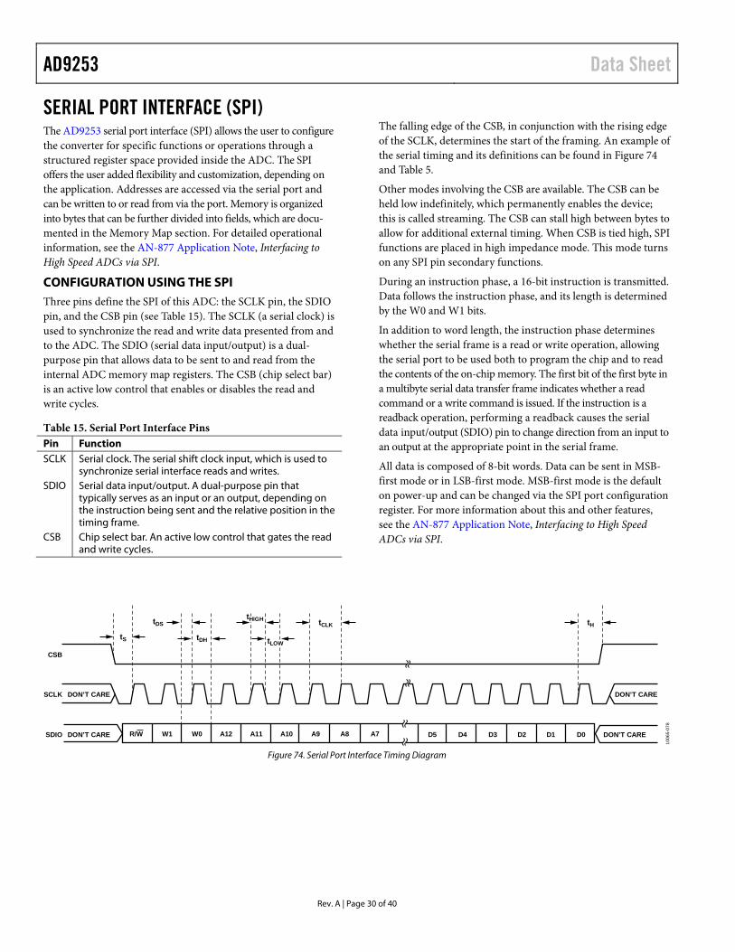
AD9253 Data Sheet
Rev. A | Page 30 of 40
SERIAL PORT INTERFACE (SPI) The AD9253 serial port interface (SPI) allows the user to configure the converter for specific functions or operations through a structured register space provided inside the ADC. The SPI offers the user added flexibility and customization, depending on the application. Addresses are accessed via the serial port and can be written to or read from via the port. Memory is organized into bytes that can be further divided into fields, which are docu-mented in the Memory Map section. For detailed operational information, see the AN-877 Application Note, Interfacing to High Speed ADCs via SPI.
CONFIGURATION USING THE SPI Three pins define the SPI of this ADC: the SCLK pin, the SDIO pin, and the CSB pin (see Table 15). The SCLK (a serial clock) is used to synchronize the read and write data presented from and to the ADC. The SDIO (serial data input/output) is a dual-purpose pin that allows data to be sent to and read from the internal ADC memory map registers. The CSB (chip select bar) is an active low control that enables or disables the read and write cycles.
Table 15. Serial Port Interface Pins Pin Function SCLK Serial clock. The serial shift clock input, which is used to
synchronize serial interface reads and writes. SDIO Serial data input/output. A dual-purpose pin that
typically serves as an input or an output, depending on the instruction being sent and the relative position in the timing frame.
CSB Chip select bar. An active low control that gates the read and write cycles.
The falling edge of the CSB, in conjunction with the rising edge of the SCLK, determines the start of the framing. An example of the serial timing and its definitions can be found in Figure 74 and Table 5.
Other modes involving the CSB are available. The CSB can be held low indefinitely, which permanently enables the device; this is called streaming. The CSB can stall high between bytes to allow for additional external timing. When CSB is tied high, SPI functions are placed in high impedance mode. This mode turns on any SPI pin secondary functions.
During an instruction phase, a 16-bit instruction is transmitted. Data follows the instruction phase, and its length is determined by the W0 and W1 bits.
In addition to word length, the instruction phase determines whether the serial frame is a read or write operation, allowing the serial port to be used both to program the chip and to read the contents of the on-chip memory. The first bit of the first byte in a multibyte serial data transfer frame indicates whether a read command or a write command is issued. If the instruction is a readback operation, performing a readback causes the serial data input/output (SDIO) pin to change direction from an input to an output at the appropriate point in the serial frame.
All data is composed of 8-bit words. Data can be sent in MSB-first mode or in LSB-first mode. MSB-first mode is the default on power-up and can be changed via the SPI port configuration register. For more information about this and other features, see the AN-877 Application Note, Interfacing to High Speed ADCs via SPI.
DON’T CARE
DON’T CAREDON’T CARE
DON’T CARE
SDIO
SCLK
CSB
tS tDH
tCLKtDS tH
R/W W1 W0 A12 A11 A10 A9 A8 A7 D5 D4 D3 D2 D1 D0
tLOW
tHIGH
1006
5-07
8
Figure 74. Serial Port Interface Timing Diagram
Data Sheet AD9253
HARDWARE INTERFACE The pins described in Table 15 comprise the physical interface between the user programming device and the serial port of the AD9253. The SCLK pin and the CSB pin function as inputs when using the SPI interface. The SDIO pin is bidirectional, functioning as an input during write phases and as an output during readback.
The SPI interface is flexible enough to be controlled by either FPGAs or microcontrollers. One method for SPI configuration is described in detail in the AN-812 Application Note, Micro-controller-Based Serial Port Interface (SPI) Boot Circuit.
The SPI port should not be active during periods when the full dynamic performance of the converter is required. Because the SCLK signal, the CSB signal, and the SDIO signal are typically asynchronous to the ADC clock, noise from these signals can degrade converter performance. If the on-board SPI bus is used for other devices, it may be necessary to provide buffers between this bus and the AD9253 to prevent these signals from transi-tioning at the converter inputs during critical sampling periods.
Some pins serve a dual function when the SPI interface is not being used. When the pins are strapped to DRVDD or ground during device power-on, they are associated with a specific function. Table 16 describes the strappable functions supported on the AD9253.
CONFIGURATION WITHOUT THE SPI In applications that do not interface to the SPI control registers, the SDIO/OLM pin, the SCLK/DTP pin, and the PDWN pin serve as standalone CMOS-compatible control pins. When the device is powered up, it is assumed that the user intends to use the pins as static control lines for the duty cycle stabilizer, output data format, and power-down feature control. In this mode, CSB should be connected to AVDD, which disables the serial port interface.
When the device is in SPI mode, the PDWN pin (if enabled) remains active. For SPI control of power-down, the PDWN pin should be set to its default state.
SPI ACCESSIBLE FEATURES Table 16 provides a brief description of the general features that are accessible via the SPI. These features are described in detail in the AN-877 Application Note, Interfacing to High Speed ADCs via SPI. The AD9253 part-specific features are described in detail following Table 17, the external memory map register table.
Table 16. Features Accessible Using the SPI Feature Name Description Power Mode Allows the user to set either power-down mode
or standby mode Clock Allows the user to access the DCS, set the
clock divider, set the clock divider phase, and enable the sync
Offset Allows the user to digitally adjust the converter offset
Test I/O Allows the user to set test modes to have known data on output bits
Output Mode Allows the user to set the output mode Output Phase Allows the user to set the output clock polarity ADC Resolution Allows for power consumption scaling with
respect to sample rate.
Rev. A | Page 31 of 40
AD9253 Data Sheet
MEMORY MAP READING THE MEMORY MAP REGISTER TABLE Each row in the memory map register table has eight bit locations. The memory map is roughly divided into three sections: the chip configuration registers (Address 0x00 to Address 0x02); the device index and transfer registers (Address 0x05 and Address 0xFF); and the global ADC functions registers, including setup, control, and test (Address 0x08 to Address 0x109).
The memory map register table (see Table 17) lists the default hexadecimal value for each hexadecimal address shown. The column with the heading Bit 7 (MSB) is the start of the default hexadecimal value given. For example, Address 0x05, the device index register, has a hexadecimal default value of 0x3F. This means that in Address 0x05, Bits[7:6] = 0, and the remaining Bits[5:0] = 1. This setting is the default channel index setting. The default value results in both ADC channels receiving the next write command. For more information on this function and others, see the AN-877 Application Note, Interfacing to High Speed ADCs via SPI. This application note details the functions controlled by Register 0x00 to Register 0xFF. The remaining registers are documented in the Memory Map Register Descriptions section.
Open Locations
All address and bit locations that are not included in Table 17 are not currently supported for this device. Unused bits of a valid address location should be written with 0s. Writing to these locations is required only when part of an address location is open (for example, Address 0x05). If the entire address location is open or not listed in Table 17 (for example, Address 0x13), this address location should not be written.
Default Values
After the AD9253 is reset, critical registers are loaded with default values. The default values for the registers are given in the memory map register table, Table 17.
Logic Levels
An explanation of logic level terminology follows:
• “Bit is set” is synonymous with “bit is set to Logic 1” or “writing Logic 1 for the bit.”
• “Clear a bit” is synonymous with “bit is set to Logic 0” or “writing Logic 0 for the bit.”
Channel-Specific Registers
Some channel setup functions can be programmed differently for each channel. In these cases, channel address locations are internally duplicated for each channel. These registers and bits are designated in Table 17 as local. These local registers and bits can be accessed by setting the appropriate data channel bits (A, B, C, or D) and the clock channel DCO bit (Bit 5) and FCO bit (Bit 4) in Register 0x05. If all the bits are set, the subsequent write affects the registers of all channels and the DCO/FCO clock channels. In a read cycle, only one of the channels (A, B, C, or D) should be set to read one of the four registers. If all the bits are set during a SPI read cycle, the part returns the value for Channel A. Registers and bits designated as global in Table 17 affect the entire part or the channel features for which independent settings are not allowed between channels. The settings in Register 0x05 do not affect the global registers and bits.
Rev. A | Page 32 of 40
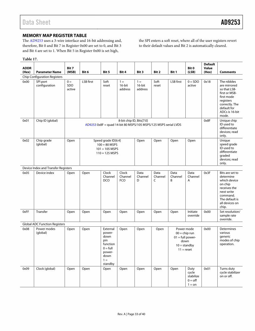
Data Sheet AD9253
MEMORY MAP REGISTER TABLE The AD9253 uses a 3-wire interface and 16-bit addressing and, therefore, Bit 0 and Bit 7 in Register 0x00 are set to 0, and Bit 3 and Bit 4 are set to 1. When Bit 5 in Register 0x00 is set high,
the SPI enters a soft reset, where all of the user registers revert to their default values and Bit 2 is automatically cleared.
Table 17.
ADDR (Hex) Parameter Name
Bit 7 (MSB) Bit 6 Bit 5 Bit 4 Bit 3 Bit 2 Bit 1
Bit 0 (LSB)
Default Value (Hex) Comments
Chip Configuration Registers
0x00 SPI port configuration
0 = SDO active
LSB first Soft reset
1 = 16-bit address
1 = 16-bit address
Soft reset
LSB first 0 = SDO active
0x18 The nibbles are mirrored so that LSB-first or MSB-first mode registers correctly. The default for ADCs is 16-bit mode.
0x01 Chip ID (global) 8-bit chip ID, Bits[7:0] AD9253 0x8F = quad 14-bit 80 MSPS/105 MSPS/125 MSPS serial LVDS
0x8F Unique chip ID used to differentiate devices; read only.
0x02 Chip grade (global)
Open Speed grade ID[6:4] 100 = 80 MSPS
101 = 105 MSPS 110 = 125 MSPS
Open Open Open Open Unique speed grade ID used to differentiate graded devices; read only.
Device Index and Transfer Registers
0x05 Device index Open Open Clock Channel DCO
Clock Channel FCO
Data Channel D
Data Channel C
Data Channel B
Data Channel A
0x3F Bits are set to determine which device on chip receives the next write command. The default is all devices on chip.
0xFF Transfer Open Open Open Open Open Open Open Initiate override
0x00 Set resolution/ sample rate override.
Global ADC Function Registers
0x08 Power modes (global)
Open Open External power-down pin function 0 = full power-down 1 = standby
Open Open Open Power mode 00 = chip run
01 = full power-down
10 = standby 11 = reset
0x00 Determines various generic modes of chip operation.
0x09 Clock (global) Open Open Open Open Open Open Open Duty cycle stabilize 0 = off 1 = on
0x01 Turns duty cycle stabilizer on or off.
Rev. A | Page 33 of 40
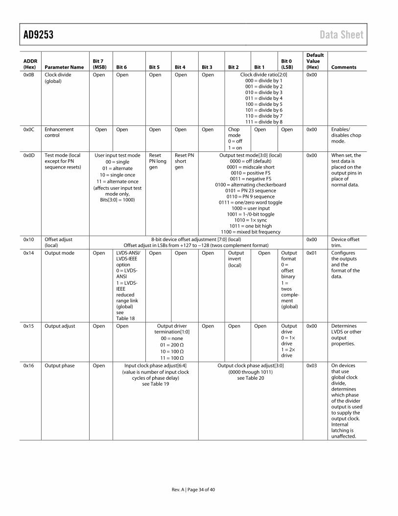
AD9253 Data Sheet
ADDR (Hex) Parameter Name
Bit 7 (MSB) Bit 6 Bit 5 Bit 4 Bit 3 Bit 2 Bit 1
Bit 0 (LSB)
Default Value (Hex) Comments
0x0B Clock divide (global)
Open Open Open Open Open Clock divide ratio[2:0] 000 = divide by 1 001 = divide by 2 010 = divide by 3 011 = divide by 4 100 = divide by 5 101 = divide by 6 110 = divide by 7 111 = divide by 8
0x00
0x0C Enhancement control
Open Open Open Open Open Chop mode 0 = off 1 = on
Open Open 0x00 Enables/ disables chop mode.
0x0D Test mode (local except for PN sequence resets)
User input test mode 00 = single
01 = alternate 10 = single once
11 = alternate once (affects user input test
mode only, Bits[3:0] = 1000)
Reset PN long gen
Reset PN short gen
Output test mode[3:0] (local) 0000 = off (default)
0001 = midscale short 0010 = positive FS 0011 = negative FS
0100 = alternating checkerboard 0101 = PN 23 sequence 0110 = PN 9 sequence
0111 = one/zero word toggle 1000 = user input
1001 = 1-/0-bit toggle 1010 = 1× sync
1011 = one bit high 1100 = mixed bit frequency
0x00 When set, the test data is placed on the output pins in place of normal data.
0x10 Offset adjust (local)
8-bit device offset adjustment [7:0] (local) Offset adjust in LSBs from +127 to −128 (twos complement format)
0x00 Device offset trim.
0x14 Output mode Open LVDS-ANSI/ LVDS-IEEE option 0 = LVDS-ANSI 1 = LVDS-IEEE reduced range link (global) see Table 18
Open Open Open Output invert (local)
Open Output format 0 = offset binary 1 = twos comple-ment (global)
0x01 Configures the outputs and the format of the data.
0x15 Output adjust Open Open Output driver termination[1:0]
00 = none 01 = 200 Ω 10 = 100 Ω 11 = 100 Ω
Open Open Open Output drive 0 = 1× drive 1 = 2× drive
0x00 Determines LVDS or other output properties.
0x16 Output phase Open Input clock phase adjust[6:4] (value is number of input clock
cycles of phase delay) see Table 19
Output clock phase adjust[3:0] (0000 through 1011)
see Table 20
0x03 On devices that use global clock divide, determines which phase of the divider output is used to supply the output clock. Internal latching is unaffected.
Rev. A | Page 34 of 40
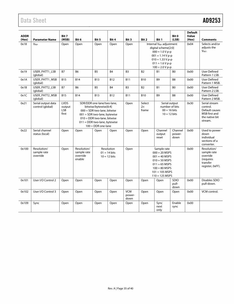
Data Sheet AD9253
ADDR (Hex) Parameter Name
Bit 7 (MSB) Bit 6 Bit 5 Bit 4 Bit 3 Bit 2 Bit 1
Bit 0 (LSB)
Default Value (Hex) Comments
0x18 VREF Open Open Open Open Open Internal VREF adjustment digital scheme[2:0]
000 = 1.0 V p-p 001 = 1.14 V p-p 010 = 1.33 V p-p 011 = 1.6 V p-p 100 = 2.0 V p-p
0x04 Selects and/or adjusts the VREF.
0x19 USER_PATT1_LSB (global)
B7 B6 B5 B4 B3 B2 B1 B0 0x00 User Defined Pattern 1 LSB.
0x1A USER_PATT1_MSB (global)
B15 B14 B13 B12 B11 B10 B9 B8 0x00 User Defined Pattern 1 MSB.
0x1B USER_PATT2_LSB (global)
B7 B6 B5 B4 B3 B2 B1 B0 0x00 User Defined Pattern 2 LSB.
0x1C USER_PATT2_MSB (global)
B15 B14 B13 B12 B11 B10 B9 B8 0x00 User Defined Pattern 2 MSB.
0x21 Serial output data control (global)
LVDS output LSB first
SDR/DDR one-lane/two-lane, bitwise/bytewise[6:4]
000 = SDR two-lane, bitwise 001 = SDR two-lane, bytewise 010 = DDR two-lane, bitwise
011 = DDR two-lane, bytewise 100 = DDR one-lane
Open Select 2× frame
Serial output number of bits
00 = 16 bits 10 = 12 bits
0x30 Serial stream control. Default causes MSB first and the native bit stream.
0x22 Serial channel status (local)
Open Open Open Open Open Open Channel output reset
Channel power-down
0x00 Used to power down individual sections of a converter.
0x100 Resolution/ sample rate override
Open Resolution/ sample rate override enable
Resolution 01 = 14 bits 10 = 12 bits
Open Sample rate 000 = 20 MSPS 001 = 40 MSPS 010 = 50 MSPS 011 = 65 MSPS 100 = 80 MSPS
101 = 105 MSPS 110 = 125 MSPS
0x00 Resolution/ sample rate override (requires transfer register, 0xFF).
0x101 User I/O Control 2 Open Open Open Open Open Open Open SDIO pull-down
0x00 Disables SDIO pull-down.
0x102 User I/O Control 3 Open Open Open Open VCM power-down
Open Open Open 0x00 VCM control.
0x109 Sync Open Open Open Open Open Open Sync next only
Enable sync
0x00
Rev. A | Page 35 of 40
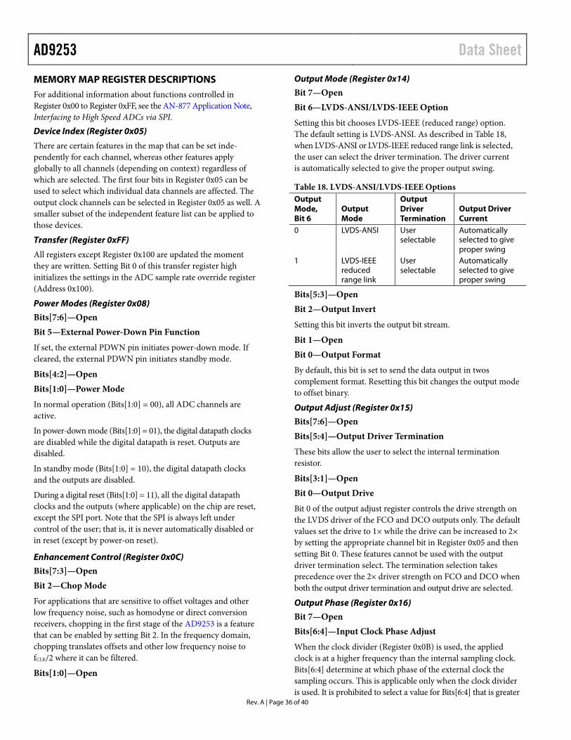
AD9253 Data Sheet
MEMORY MAP REGISTER DESCRIPTIONS For additional information about functions controlled in Register 0x00 to Register 0xFF, see the AN-877 Application Note, Interfacing to High Speed ADCs via SPI.
Device Index (Register 0x05)
There are certain features in the map that can be set inde-pendently for each channel, whereas other features apply globally to all channels (depending on context) regardless of which are selected. The first four bits in Register 0x05 can be used to select which individual data channels are affected. The output clock channels can be selected in Register 0x05 as well. A smaller subset of the independent feature list can be applied to those devices.
Transfer (Register 0xFF)
All registers except Register 0x100 are updated the moment they are written. Setting Bit 0 of this transfer register high initializes the settings in the ADC sample rate override register (Address 0x100).
Power Modes (Register 0x08)
Bits[7:6]—Open Bit 5—External Power-Down Pin Function
If set, the external PDWN pin initiates power-down mode. If cleared, the external PDWN pin initiates standby mode.
Bits[4:2]—Open Bits[1:0]—Power Mode
In normal operation (Bits[1:0] = 00), all ADC channels are active.
In power-down mode (Bits[1:0] = 01), the digital datapath clocks are disabled while the digital datapath is reset. Outputs are disabled.
In standby mode (Bits[1:0] = 10), the digital datapath clocks and the outputs are disabled.
During a digital reset (Bits[1:0] = 11), all the digital datapath clocks and the outputs (where applicable) on the chip are reset, except the SPI port. Note that the SPI is always left under control of the user; that is, it is never automatically disabled or in reset (except by power-on reset).
Enhancement Control (Register 0x0C)
Bits[7:3]—Open Bit 2—Chop Mode
For applications that are sensitive to offset voltages and other low frequency noise, such as homodyne or direct conversion receivers, chopping in the first stage of the AD9253 is a feature that can be enabled by setting Bit 2. In the frequency domain, chopping translates offsets and other low frequency noise to fCLK/2 where it can be filtered.
Bits[1:0]—Open
Output Mode (Register 0x14)
Bit 7—Open Bit 6—LVDS-ANSI/LVDS-IEEE Option
Setting this bit chooses LVDS-IEEE (reduced range) option. The default setting is LVDS-ANSI. As described in Table 18, when LVDS-ANSI or LVDS-IEEE reduced range link is selected, the user can select the driver termination. The driver current is automatically selected to give the proper output swing.
Table 18. LVDS-ANSI/LVDS-IEEE Options Output Mode, Bit 6
Output Mode
Output Driver Termination
Output Driver Current
0 LVDS-ANSI User selectable
Automatically selected to give proper swing
1 LVDS-IEEE reduced range link
User selectable
Automatically selected to give proper swing
Bits[5:3]—Open Bit 2—Output Invert
Setting this bit inverts the output bit stream.
Bit 1—Open Bit 0—Output Format
By default, this bit is set to send the data output in twos complement format. Resetting this bit changes the output mode to offset binary.
Output Adjust (Register 0x15)
Bits[7:6]—Open Bits[5:4]—Output Driver Termination
These bits allow the user to select the internal termination resistor.
Bits[3:1]—Open Bit 0—Output Drive
Bit 0 of the output adjust register controls the drive strength on the LVDS driver of the FCO and DCO outputs only. The default values set the drive to 1× while the drive can be increased to 2× by setting the appropriate channel bit in Register 0x05 and then setting Bit 0. These features cannot be used with the output driver termination select. The termination selection takes precedence over the 2× driver strength on FCO and DCO when both the output driver termination and output drive are selected.
Output Phase (Register 0x16)
Bit 7—Open Bits[6:4]—Input Clock Phase Adjust
When the clock divider (Register 0x0B) is used, the applied clock is at a higher frequency than the internal sampling clock. Bits[6:4] determine at which phase of the external clock the sampling occurs. This is applicable only when the clock divider is used. It is prohibited to select a value for Bits[6:4] that is greater
Rev. A | Page 36 of 40
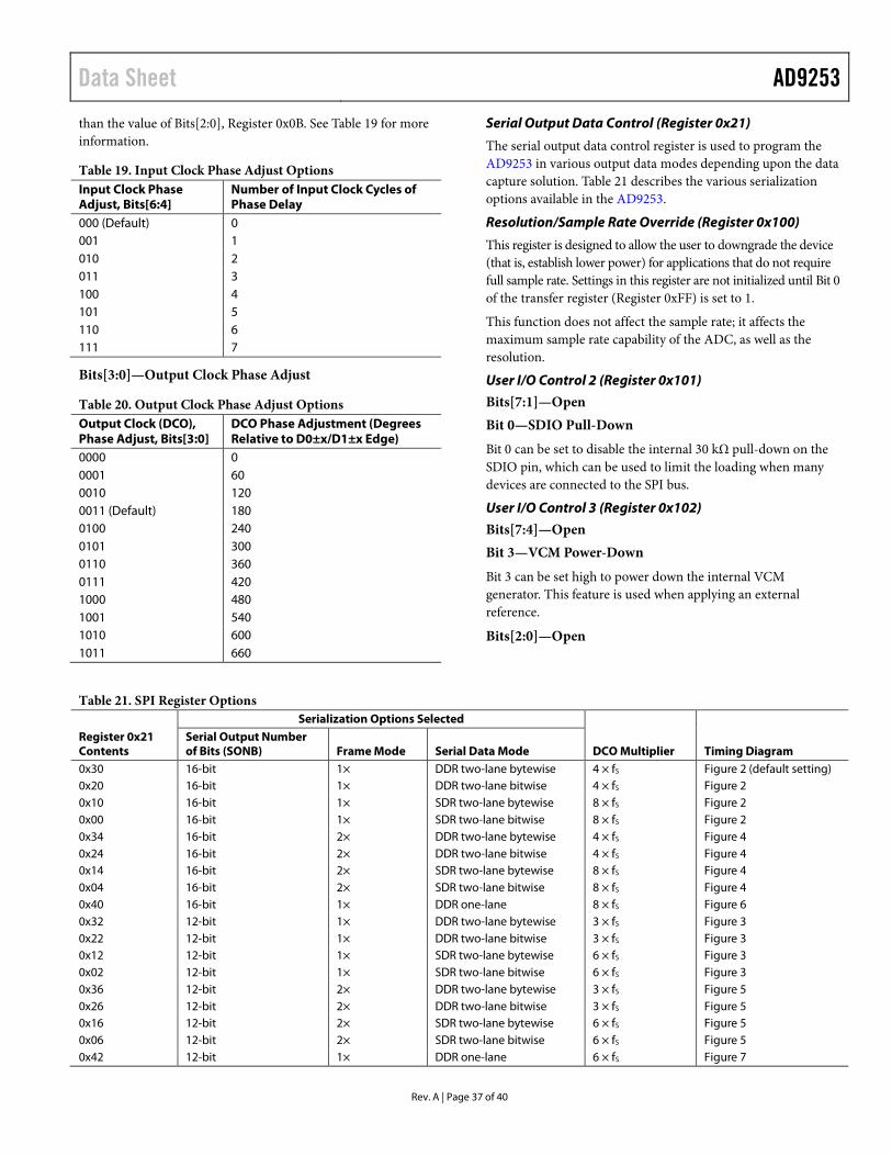
Data Sheet AD9253 than the value of Bits[2:0], Register 0x0B. See Table 19 for more information.
Table 19. Input Clock Phase Adjust Options Input Clock Phase Adjust, Bits[6:4]
Number of Input Clock Cycles of Phase Delay
000 (Default) 0 001 1 010 2 011 3 100 4 101 5 110 6 111 7
Bits[3:0]—Output Clock Phase Adjust
Table 20. Output Clock Phase Adjust Options Output Clock (DCO), Phase Adjust, Bits[3:0]
DCO Phase Adjustment (Degrees Relative to D0±x/D1±x Edge)
0000 0 0001 60 0010 120 0011 (Default) 180 0100 240 0101 300 0110 360 0111 420 1000 480 1001 540 1010 600 1011 660
Serial Output Data Control (Register 0x21)
The serial output data control register is used to program the AD9253 in various output data modes depending upon the data capture solution. Table 21 describes the various serialization options available in the AD9253.
Resolution/Sample Rate Override (Register 0x100)
This register is designed to allow the user to downgrade the device (that is, establish lower power) for applications that do not require full sample rate. Settings in this register are not initialized until Bit 0 of the transfer register (Register 0xFF) is set to 1.
This function does not affect the sample rate; it affects the maximum sample rate capability of the ADC, as well as the resolution.
User I/O Control 2 (Register 0x101)
Bits[7:1]—Open Bit 0—SDIO Pull-Down
Bit 0 can be set to disable the internal 30 kΩ pull-down on the SDIO pin, which can be used to limit the loading when many devices are connected to the SPI bus.
User I/O Control 3 (Register 0x102)
Bits[7:4]—Open Bit 3—VCM Power-Down
Bit 3 can be set high to power down the internal VCM generator. This feature is used when applying an external reference.
Bits[2:0]—Open
Table 21. SPI Register Options Serialization Options Selected
Register 0x21 Contents
Serial Output Number of Bits (SONB) Frame Mode Serial Data Mode DCO Multiplier Timing Diagram
0x30 16-bit 1× DDR two-lane bytewise 4 × fS Figure 2 (default setting) 0x20 16-bit 1× DDR two-lane bitwise 4 × fS Figure 2 0x10 16-bit 1× SDR two-lane bytewise 8 × fS Figure 2 0x00 16-bit 1× SDR two-lane bitwise 8 × fS Figure 2 0x34 16-bit 2× DDR two-lane bytewise 4 × fS Figure 4 0x24 16-bit 2× DDR two-lane bitwise 4 × fS Figure 4 0x14 16-bit 2× SDR two-lane bytewise 8 × fS Figure 4 0x04 16-bit 2× SDR two-lane bitwise 8 × fS Figure 4 0x40 16-bit 1× DDR one-lane 8 × fS Figure 6 0x32 12-bit 1× DDR two-lane bytewise 3 × fS Figure 3 0x22 12-bit 1× DDR two-lane bitwise 3 × fS Figure 3 0x12 12-bit 1× SDR two-lane bytewise 6 × fS Figure 3 0x02 12-bit 1× SDR two-lane bitwise 6 × fS Figure 3 0x36 12-bit 2× DDR two-lane bytewise 3 × fS Figure 5 0x26 12-bit 2× DDR two-lane bitwise 3 × fS Figure 5 0x16 12-bit 2× SDR two-lane bytewise 6 × fS Figure 5 0x06 12-bit 2× SDR two-lane bitwise 6 × fS Figure 5 0x42 12-bit 1× DDR one-lane 6 × fS Figure 7
Rev. A | Page 37 of 40
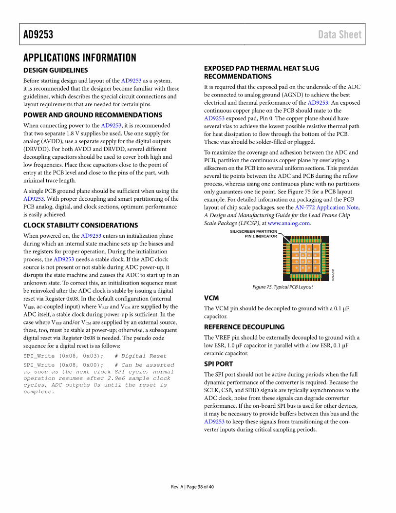
AD9253 Data Sheet
APPLICATIONS INFORMATION DESIGN GUIDELINES Before starting design and layout of the AD9253 as a system, it is recommended that the designer become familiar with these guidelines, which describes the special circuit connections and layout requirements that are needed for certain pins.
POWER AND GROUND RECOMMENDATIONS When connecting power to the AD9253, it is recommended that two separate 1.8 V supplies be used. Use one supply for analog (AVDD); use a separate supply for the digital outputs (DRVDD). For both AVDD and DRVDD, several different decoupling capacitors should be used to cover both high and low frequencies. Place these capacitors close to the point of entry at the PCB level and close to the pins of the part, with minimal trace length.
A single PCB ground plane should be sufficient when using the AD9253. With proper decoupling and smart partitioning of the PCB analog, digital, and clock sections, optimum performance is easily achieved.
CLOCK STABILITY CONSIDERATIONS When powered on, the AD9253 enters an initialization phase during which an internal state machine sets up the biases and the registers for proper operation. During the initialization process, the AD9253 needs a stable clock. If the ADC clock source is not present or not stable during ADC power-up, it disrupts the state machine and causes the ADC to start up in an unknown state. To correct this, an initialization sequence must be reinvoked after the ADC clock is stable by issuing a digital reset via Register 0x08. In the default configuration (internal VREF, ac-coupled input) where VREF and VCM are supplied by the ADC itself, a stable clock during power-up is sufficient. In the case where VREF and/or VCM are supplied by an external source, these, too, must be stable at power-up; otherwise, a subsequent digital reset via Register 0x08 is needed. The pseudo code sequence for a digital reset is as follows:
SPI_Write (0x08, 0x03); # Digital Reset
SPI_Write (0x08, 0x00); # Can be asserted as soon as the next clock SPI cycle, normal operation resumes after 2.9e6 sample clock cycles, ADC outputs 0s until the reset is complete.
EXPOSED PAD THERMAL HEAT SLUG RECOMMENDATIONS It is required that the exposed pad on the underside of the ADC be connected to analog ground (AGND) to achieve the best electrical and thermal performance of the AD9253. An exposed continuous copper plane on the PCB should mate to the AD9253 exposed pad, Pin 0. The copper plane should have several vias to achieve the lowest possible resistive thermal path for heat dissipation to flow through the bottom of the PCB. These vias should be solder-filled or plugged.
To maximize the coverage and adhesion between the ADC and PCB, partition the continuous copper plane by overlaying a silkscreen on the PCB into several uniform sections. This provides several tie points between the ADC and PCB during the reflow process, whereas using one continuous plane with no partitions only guarantees one tie point. See Figure 75 for a PCB layout example. For detailed information on packaging and the PCB layout of chip scale packages, see the AN-772 Application Note, A Design and Manufacturing Guide for the Lead Frame Chip Scale Package (LFCSP), at www.analog.com.
SILKSCREEN PARTITIONPIN 1 INDICATOR
1006
5-08
0
Figure 75. Typical PCB Layout
VCM The VCM pin should be decoupled to ground with a 0.1 μF capacitor.
REFERENCE DECOUPLING The VREF pin should be externally decoupled to ground with a low ESR, 1.0 μF capacitor in parallel with a low ESR, 0.1 μF ceramic capacitor.
SPI PORT The SPI port should not be active during periods when the full dynamic performance of the converter is required. Because the SCLK, CSB, and SDIO signals are typically asynchronous to the ADC clock, noise from these signals can degrade converter performance. If the on-board SPI bus is used for other devices, it may be necessary to provide buffers between this bus and the AD9253 to keep these signals from transitioning at the con-verter inputs during critical sampling periods.
Rev. A | Page 38 of 40
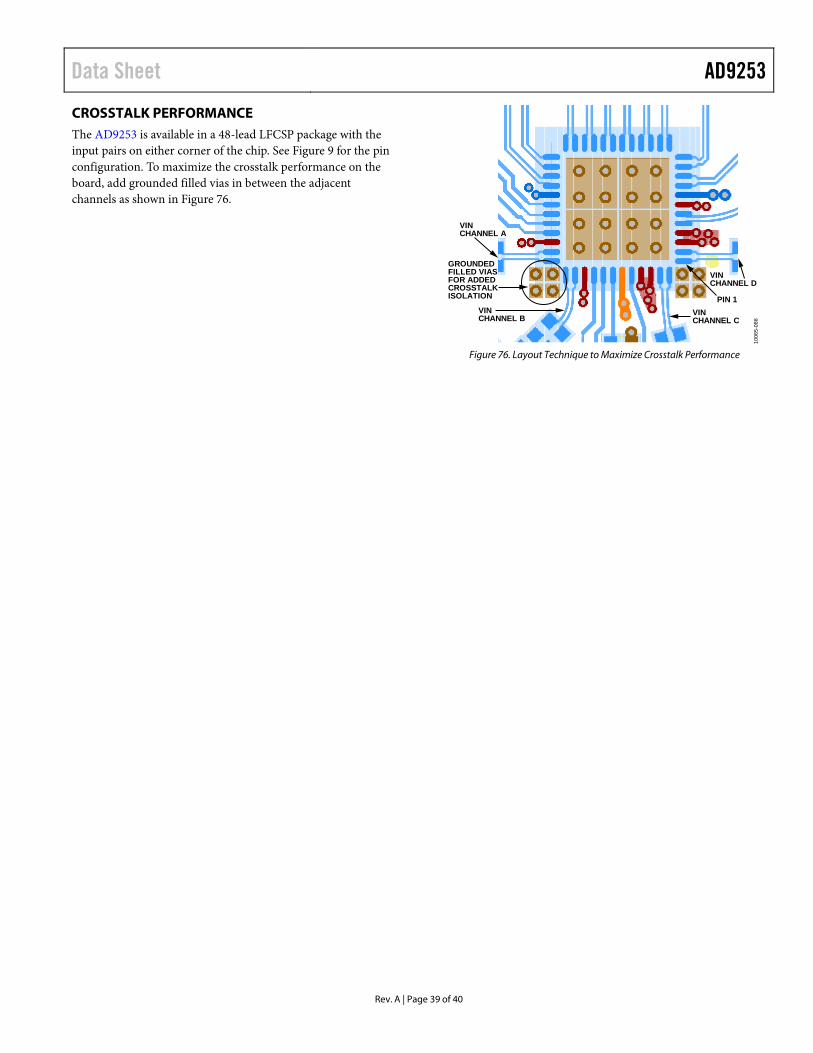
Data Sheet AD9253
CROSSTALK PERFORMANCE The AD9253 is available in a 48-lead LFCSP package with the input pairs on either corner of the chip. See Figure 9 for the pin configuration. To maximize the crosstalk performance on the board, add grounded filled vias in between the adjacent channels as shown in Figure 76.
GROUNDEDFILLED VIASFOR ADDEDCROSSTALKISOLATION
VINCHANNEL B
VINCHANNEL C
VINCHANNEL A
VINCHANNEL D
PIN 1
1006
5-08
8
Figure 76. Layout Technique to Maximize Crosstalk Performance
Rev. A | Page 39 of 40
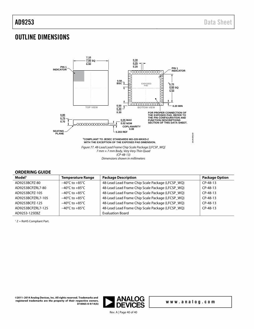
AD9253 Data Sheet
Rev. A | Page 40 of 40
OUTLINE DIMENSIONS
1
0.50BSC
BOTTOM VIEWTOP VIEW
PIN 1INDICATOR
48
1324
3637
EXPOSEDPAD
PIN 1INDICATOR
*5.705.60 SQ5.50
0.500.400.30
SEATINGPLANE
0.800.750.70 0.05 MAX
0.02 NOM
0.203 REF
COPLANARITY0.08
0.300.250.20
10-2
4-20
13-D
7.107.00 SQ6.90
FOR PROPER CONNECTION OFTHE EXPOSED PAD, REFER TOTHE PIN CONFIGURATION ANDFUNCTION DESCRIPTIONSSECTION OF THIS DATA SHEET.
0.20 MIN
*COMPLIANT TO JEDEC STANDARDS MO-220-WKKD-2WITH THE EXCEPTION OF THE EXPOSED PAD DIMENSION.
Figure 77. 48-Lead Lead Frame Chip Scale Package [LFCSP_WQ] 7 mm × 7 mm Body, Very Very Thin Quad
(CP-48-13) Dimensions shown in millimeters
ORDERING GUIDE Model1 Temperature Range Package Description Package Option AD9253BCPZ-80 −40°C to +85°C 48-Lead Lead Frame Chip Scale Package (LFCSP_WQ) CP-48-13 AD9253BCPZRL7-80 −40°C to +85°C 48-Lead Lead Frame Chip Scale Package (LFCSP_WQ) CP-48-13 AD9253BCPZ-105 −40°C to +85°C 48-Lead Lead Frame Chip Scale Package (LFCSP_WQ) CP-48-13 AD9253BCPZRL7-105 −40°C to +85°C 48-Lead Lead Frame Chip Scale Package (LFCSP_WQ) CP-48-13 AD9253BCPZ-125 −40°C to +85°C 48-Lead Lead Frame Chip Scale Package (LFCSP_WQ) CP-48-13 AD9253BCPZRL7-125 −40°C to +85°C 48-Lead Lead Frame Chip Scale Package (LFCSP_WQ) CP-48-13 AD9253-125EBZ Evaluation Board 1 Z = RoHS Compliant Part.
©2011–2014 Analog Devices, Inc. All rights reserved. Trademarks and registered trademarks are the property of their respective owners. D10065-0-9/14(A)
Related Documents