Pupil wavefront manipulation for optical nanolithography Monica Kempsell Sears a *, Joost Bekaert b , Bruce W. Smith a a RIT, Microsystems Engineering, 77 Lomb Memorial Drive, Rochester, NY 14623 b IMEC vzw, Kapeldreef 75, 3001 Leuven, Belgium *[email protected] ABSTRACT As semiconductor lithography is pushed to smaller dimensions, process yields tend to suffer due to sub- wavelength topographical imaging effects. Three dimensional or “thick mask” effects result in such things as a pitch dependent best focus and, for alternating phase shift masks (AltPSMs), an intensity imbalance between etched and un-etched features. Corrective mask structures such as the dual trench AltPSM have been introduced to compensate for such intensity imbalances. In this work, the compensation of thick mask effects is explored using the manipulation of the pupil wavefront through the addition of spherical aberration. The wavefront has been experimentally varied through the manipulation of the lens aberration in a state of the art full field scanner. Results reveal that the influence of spherical aberration on best focus is predictable, allowing focus deviation through pitch to be tuned. Simulations further predict that aberration manipulation can provide compensation for thick mask effects by increasing the useable depth of focus for a particular set of features on both AltPSM and thicker film attenuated PSM masks. Such pupil wavefront correction has the potential to compensate for mask topography by matching thick mask effects to those of thin masks. Keywords: Focus Exposure Matrix (FEM) tilt, thick mask effects, spherical aberration, mask topography, lens pupil domain, AltPSM, AttPSM, Binary 1. INTRODUCTION Mask topography effects have gained significant attention with advanced technology nodes due to the imaging challenges that arise for thick masks. For an AltPSM, the intensity imbalance between the etched and un-etched spaces result in a degraded useable depth of focus (UDOF) [1]. Mask stacks that avoid this intensity imbalance have been developed, such as dual trench (DT) AltPSM and Sidewall Chrome Alternating Aperture Mask (SCAAM), but require multiple etch steps and therefore are complex to fabricate [2, 3]. A thick mask stack can also cause a pitch dependent best focus [4]. A bi-layer attenuated phase shift mask made up of an absorber layer, such as Ta, and a transparent layer, such as SiON, provides independent tuning of the attenuation and phase [5]. Experimental work has shown that a TaSiON mask provides an exposure latitude (EL) improvement over standard films (6% MoSi attenuated PSM and Cr/CrO binary) [6]. However, the improvement does not extend to more isolated pitches, due to a mask transmission resonance that can manifest as negative MEEF [7]. These thick mask effects have resulted in a trend towards thinner masking layers, constraining optical properties to thin films well below exposing wavelengths. Restricting the mask thickness leads to a narrow choice of materials that possess appropriate complex optical constants (n and k). In addition, it becomes more difficult to control attenuation and phase independently as can be done with a multiple layer film stack. This work alternatively explores compensation methods through pupil wavefront manipulation, specifically in the form of spherical aberration in the projection lens. 2. THEORY When features on a mask are on the order of the illumination wavelength, surface topography creates effects correlatable to optical aberrations, which can induce asymmetry in the Focus Exposure Matrix (FEM) [8]. This is seen in a single trench (ST) AltPSM, which exhibits an intensity imbalance between the etched and un-etched spaces [9]. This intensity imbalance is due to a non-zero diffraction order resulting from light scattering from the quartz edges of the etched feature towards the un-etched feature [10-12]. For small features with k 1 values below 0.35, a pitch dependent best focus (BF) has been experimentally observed [13]. This can be attributed to spherical aberration

Welcome message from author
This document is posted to help you gain knowledge. Please leave a comment to let me know what you think about it! Share it to your friends and learn new things together.
Transcript

Pupil wavefront manipulation for optical nanolithography
Monica Kempsell Sears
a*, Joost Bekaert
b, Bruce W. Smith
a
aRIT, Microsystems Engineering, 77 Lomb Memorial Drive, Rochester, NY 14623
bIMEC vzw, Kapeldreef 75, 3001 Leuven, Belgium
ABSTRACT
As semiconductor lithography is pushed to smaller dimensions, process yields tend to suffer due to sub-
wavelength topographical imaging effects. Three dimensional or “thick mask” effects result in such things as a pitch
dependent best focus and, for alternating phase shift masks (AltPSMs), an intensity imbalance between etched and
un-etched features. Corrective mask structures such as the dual trench AltPSM have been introduced to compensate
for such intensity imbalances. In this work, the compensation of thick mask effects is explored using the
manipulation of the pupil wavefront through the addition of spherical aberration. The wavefront has been
experimentally varied through the manipulation of the lens aberration in a state of the art full field scanner. Results
reveal that the influence of spherical aberration on best focus is predictable, allowing focus deviation through pitch
to be tuned. Simulations further predict that aberration manipulation can provide compensation for thick mask
effects by increasing the useable depth of focus for a particular set of features on both AltPSM and thicker film
attenuated PSM masks. Such pupil wavefront correction has the potential to compensate for mask topography by
matching thick mask effects to those of thin masks.
Keywords: Focus Exposure Matrix (FEM) tilt, thick mask effects, spherical aberration, mask topography, lens pupil
domain, AltPSM, AttPSM, Binary
1. INTRODUCTION
Mask topography effects have gained significant attention with advanced technology nodes due to the imaging
challenges that arise for thick masks. For an AltPSM, the intensity imbalance between the etched and un-etched
spaces result in a degraded useable depth of focus (UDOF) [1]. Mask stacks that avoid this intensity imbalance have
been developed, such as dual trench (DT) AltPSM and Sidewall Chrome Alternating Aperture Mask (SCAAM), but
require multiple etch steps and therefore are complex to fabricate [2, 3]. A thick mask stack can also cause a pitch
dependent best focus [4]. A bi-layer attenuated phase shift mask made up of an absorber layer, such as Ta, and a
transparent layer, such as SiON, provides independent tuning of the attenuation and phase [5]. Experimental work
has shown that a TaSiON mask provides an exposure latitude (EL) improvement over standard films (6% MoSi
attenuated PSM and Cr/CrO binary) [6]. However, the improvement does not extend to more isolated pitches, due to
a mask transmission resonance that can manifest as negative MEEF [7].
These thick mask effects have resulted in a trend towards thinner masking layers, constraining optical properties
to thin films well below exposing wavelengths. Restricting the mask thickness leads to a narrow choice of materials
that possess appropriate complex optical constants (n and k). In addition, it becomes more difficult to control
attenuation and phase independently as can be done with a multiple layer film stack. This work alternatively explores
compensation methods through pupil wavefront manipulation, specifically in the form of spherical aberration in the
projection lens.
2. THEORY
When features on a mask are on the order of the illumination wavelength, surface topography creates effects
correlatable to optical aberrations, which can induce asymmetry in the Focus Exposure Matrix (FEM) [8]. This is
seen in a single trench (ST) AltPSM, which exhibits an intensity imbalance between the etched and un-etched spaces
[9]. This intensity imbalance is due to a non-zero diffraction order resulting from light scattering from the quartz
edges of the etched feature towards the un-etched feature [10-12]. For small features with k1 values below 0.35, a
pitch dependent best focus (BF) has been experimentally observed [13]. This can be attributed to spherical aberration
effects induced by the mask topography, manifested as a variation in defocus at increasing radial locations in the lens
pupil [14].
The major lithographic effects from spherical aberration include a pitch dependent best focus shift as well as a
decrease in DOF [15]. Experimental measurement of FEM Tilt, also called isofocal tilt, has been used to provide a
qualification of the amount of spherical aberration in the system [16]. Primary spherical aberration as a function of
pupil radius, ρ, is described using the Zernike polynomial z9 (6ρ4
- 6ρ2+1), where z9 is the spherical aberration
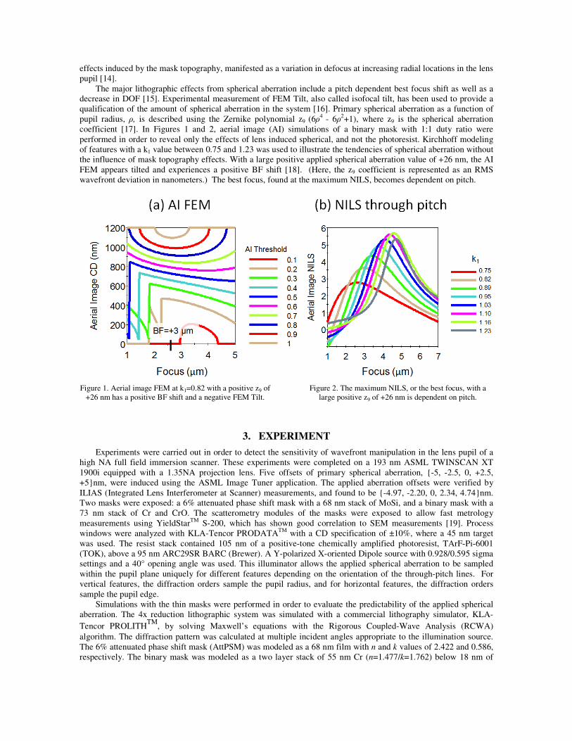
coefficient [17]. In Figures 1 and 2, aerial image (AI) simulations of a binary mask with 1:1 duty ratio were
performed in order to reveal only the effects of lens induced spherical, and not the photoresist. Kirchhoff modeling
of features with a k1 value between 0.75 and 1.23 was used to illustrate the tendencies of spherical aberration without
the influence of mask topography effects. With a large positive applied spherical aberration value of +26 nm, the AI
FEM appears tilted and experiences a positive BF shift [18]. (Here, the z9 coefficient is represented as an RMS
wavefront deviation in nanometers.) The best focus, found at the maximum NILS, becomes dependent on pitch.
Figure 1. Aerial image FEM at k1=0.82 with a positive z9 of
+26 nm has a positive BF shift and a negative FEM Tilt.
Figure 2. The maximum NILS, or the best focus, with a
large positive z9 of +26 nm is dependent on pitch.
3. EXPERIMENT
Experiments were carried out in order to detect the sensitivity of wavefront manipulation in the lens pupil of a
high NA full field immersion scanner. These experiments were completed on a 193 nm ASML TWINSCAN XT
1900i equipped with a 1.35NA projection lens. Five offsets of primary spherical aberration, {-5, -2.5, 0, +2.5,
+5}nm, were induced using the ASML Image Tuner application. The applied aberration offsets were verified by
ILIAS (Integrated Lens Interferometer at Scanner) measurements, and found to be {-4.97, -2.20, 0, 2.34, 4.74}nm.
Two masks were exposed: a 6% attenuated phase shift mask with a 68 nm stack of MoSi, and a binary mask with a
73 nm stack of Cr and CrO. The scatterometry modules of the masks were exposed to allow fast metrology
measurements using YieldStarTM
S-200, which has shown good correlation to SEM measurements [19]. Process
windows were analyzed with KLA-Tencor PRODATATM
with a CD specification of ±10%, where a 45 nm target
was used. The resist stack contained 105 nm of a positive-tone chemically amplified photoresist, TArF-Pi-6001
(TOK), above a 95 nm ARC29SR BARC (Brewer). A Y-polarized X-oriented Dipole source with 0.928/0.595 sigma
settings and a 40° opening angle was used. This illuminator allows the applied spherical aberration to be sampled
within the pupil plane uniquely for different features depending on the orientation of the through-pitch lines. For
vertical features, the diffraction orders sample the pupil radius, and for horizontal features, the diffraction orders
sample the pupil edge.
Simulations with the thin masks were performed in order to evaluate the predictability of the applied spherical
aberration. The 4x reduction lithographic system was simulated with a commercial lithography simulator, KLA-
Tencor PROLITHTM
, by solving Maxwell’s equations with the Rigorous Coupled-Wave Analysis (RCWA)
algorithm. The diffraction pattern was calculated at multiple incident angles appropriate to the illumination source.
The 6% attenuated phase shift mask (AttPSM) was modeled as a 68 nm film with n and k values of 2.422 and 0.586,
respectively. The binary mask was modeled as a two layer stack of 55 nm Cr (n=1.477/k=1.762) below 18 nm of

CrO (n=1.965/k=1.201). The raw data of the applied illuminator on the tool was used as the simulated source. The
DOF and BF were extracted with exposure latitude of 5% for both data and simulation of the thin masks.
Simulations with thick mask stacks were performed in order to explore mask topography compensation. Two
mask types with on-wafer target 45 nm lines through pitch were evaluated in a 1.35NA system: a strong alternating
PSM and a 1% attenuated PSM. The 45 nm lines on the AltPSM were unbiased to keep the intensity imbalance
present, whereas the 45 nm lines through pitch on the thick 1% attenuated PSM were biased to print at the same
exposure. The absorber of the AltPSM was modeled as the 73 nm Cr/CrO stack, and the illumination was a Y-
polarized conventional source with 0.3σ. The 1% attenuated mask stack contained 34 nm of Ta under 113.5 nm of
SiON, and the illumination was an XY polarized cross quadrupole aperture (C-quad) with inner and outer sigma
values of 0.86 and 0.66, at a 30° opening angle. A calibrated resist model based on the experimental stack was used.
The rigorously simulated best focus values of the thick masks were extracted with exposure latitude of 3%.
4. RESULTS AND DISCUSSION
4.1 Experimental thin mask data
The influence of spherical aberration on the tilt of the FEM was observed in the data. For example, Figure 3
shows the process window for a vertical pitch of 160 nm on the 6% AttPSM at both a spherical value of -5 nm and
+5 nm. The process window shows a larger linear tilt at the negative value when compared to the positive value of
spherical aberration. The FEM Tilt was quantified by fitting a polynomial to the process window and extracting the
linear coefficient as the Tilt. Extracted Tilt as a function of z9 for several vertical pitches is shown to be pitch
dependent in Figure 4. The FEM Tilt tends to be higher with a negative value of spherical aberration. For the large
pitches of 280 and 400 nm, the FEM Tilt remains low even with -5 nm of spherical aberration. This is due to the
location of the diffraction orders in the pupil plane relative to the fingerprint of spherical aberration. For these
pitches with the above mentioned dipole illumination, the zero and first orders lie symmetric about spherical
aberration’s minimum. The effect from spherical is reduced since similar phases are induced on the orders. For the
160 nm pitch, the first diffraction order is near the middle of the pupil, which is a maximum in spherical aberration’s
fingerprint, so it sees a higher phase value than the zero diffraction order, leading to a larger FEM Tilt effect.
Figure 3. Experimental process window for vertical pitch
of 160 nm at an applied spherical aberration of -5 nm is
more tilted than that of +5nm.
Figure 4. Extracted tilt for a variety of vertical pitches tends
to be higher at a negative applied spherical.
Figure 5 shows the process window for a horizontal pitch of 170 nm at both a spherical value of -5 nm and +5
nm. The process window shows a higher tilt at the positive z9 value compared to the negative z9 value. Extracted
Tilt values for several horizontal pitches are shown in Figure 6. The FEM Tilt tends to be higher at a positive value
of spherical aberration. The FEM Tilt of horizontal pitches has the opposite relationship to spherical than vertical
pitches due to the location of the diffraction orders in the pupil. For vertical pitches, the first diffraction orders lie
along the radius of the pupil, whereas for horizontal pitches the first diffraction orders lie along the edge of the pupil.
Spherical aberration has the opposite slope in these two regions, resulting in the opposite FEM Tilt tendency. The
FEM Tilt trend for horizontal pitches is similar through pitch because the first diffraction order is always at a large
pupil radius.
Figure 5. Experimental process window for horizontal
pitch of 170 nm at an applied spherical aberration of +5 nm
is more tilted than that of -5nm.
Figure 6. Extracted tilt for a variety of pitches tends to be
higher at a positive applied spherical aberration.
Applied spherical aberration results in a best focus shift, which depends on the pitch and orientation of the
features. Figure 7 shows that the best focus for a vertical pitch of 280 nm shifts negative with a positive applied
spherical. Figure 8 shows that the best focus for a horizontal pitch of 280 nm shifts in the opposite direction. Again,
this is due to the different regions of spherical that the first diffraction orders encounter, which have the opposite
slope.
Figure 7. Process windows for vertical pitch of 280 nm
shift negative in focus with increasing spherical aberration.
Figure 8. Process windows for horizontal pitch of 280 nm
shift positive in focus with increasing spherical aberration.
The experimental best focus for several pitches is plotted with simulated values for both orientations in Figures
11 and 12. The simulation predicts a linear relationship between best focus and spherical. The experimental best
focus is plotted together with trend lines for the vertical orientation in Figures 9 and 10. Note that the data for each
offset of spherical aberration was taken on different wafers. Removing the data from the z9=0 wafer increases the
average trend line R2 value from 0.73 to 0.95, suggesting that the z9=0 wafer may be an outlier. In Figure 11, the
focus versus spherical slope for vertical features is dependent on pitch, which is characteristic of spherical
aberration. The best focus deviation through pitch, or ΔBF, is minimized with a positive offset of spherical, which is
the same offset of spherical which minimized FEM Tilt in Figure 4. For horizontal pitches, the focus versus spherical
slope is not dependent on pitch due to the limited pupil radial sampling, thus reveals a defocus-like trend.

Figure 9. Experimental best focus (points) for vertical
pitches is plotted with linear regression (dotted lines). The
average R2 value is 0.73.
Figure 10. Experimental best focus (points) without z9=0
data plotted with linear regression (dotted lines). The
average R2 value increased to 0.95.
Figure 11. Experimental best focus (points) for vertical
pitches is plotted with simulated values (lines). Pitch
dependent best focus characteristic of spherical is present.
Figure 12. Experimental best focus (points) for horizontal
pitches is plotted with simulated values (lines). Spherical
effect is minimal due to limited radial sampling
The experimental best focus for the exposures on a binary mask is plotted with simulation in Figures 13 and 14.
The zero z9 data for the vertical pitches was removed, increasing the average R2 from a trend line from 0.39 to 0.92.
The best focus through spherical slope is similar to the AttPSM; negative slope for vertical pitches and positive slope
for horizontal pitches. The ∆BF for vertical pitches is minimized with a positive value of spherical and the horizontal
pitches reveal less spherical effect due to limited radial sampling of the pupil.
Figure 13. Experimental best focus for binary vertical
pitches is plotted with simulated values. Pitch dependent
best focus characteristic of spherical is present.
Figure 14. Experimental best focus for binary horizontal
pitches plotted with simulation. Spherical effect is minimal
due to less pupil radius values probed through pitch.
The best focus was measured for the CD and length of line end features on the 6% AttPSM, shown in Figure 15.
The influence of spherical can be seen as the pitch dependent slope of BF. Similar to the 6% AttPSM vertical
pitches, the ∆BF is reduced with a positive amount of spherical aberration. For both the binary and AttPSM masks,
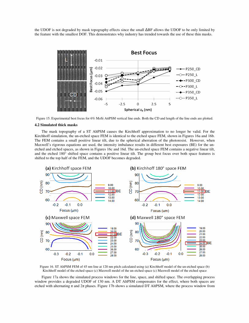
the UDOF is not degraded by mask topography effects since the small ∆BF allows the UDOF to be only limited by
the feature with the smallest DOF. This demonstrates why industry has trended towards the use of these thin masks.
Figure 15. Experimental best focus for 6% MoSi AttPSM vertical line ends. Both the CD and length of the line ends are plotted.
4.2 Simulated thick masks
The mask topography of a ST AltPSM causes the Kirchhoff approximation to no longer be valid. For the
Kirchhoff simulation, the un-etched space FEM is identical to the etched space FEM, shown in Figures 16a and 16b.
The FEM contains a small positive linear tilt, due to the spherical aberration of the photoresist. However, when
Maxwell’s rigorous equations are used, the intensity imbalance results in different best exposures (BE) for the un-
etched and etched spaces, as shown in Figures 16c and 16d. The un-etched space FEM contains a negative linear tilt,
and the etched 180° shifted space contains a positive linear tilt. The group best focus over both space features is
shifted to the top half of the FEM, and the UDOF becomes degraded.
Figure 16. ST AltPSM FEM of 45 nm line at 120 nm pitch calculated using (a) Kirchhoff model of the un-etched space (b)
Kirchhoff model of the etched space (c) Maxwell model of the un-etched space (c) Maxwell model of the etched space
Figure 17a shows the simulated process windows for the line, space, and shifted space. The overlapping process
window provides a degraded UDOF of 130 nm. A DT AltPSM compensates for the effect, where both spaces are
etched with alternating π and 2π phases. Figure 17b shows a simulated DT AltPSM, where the process window from
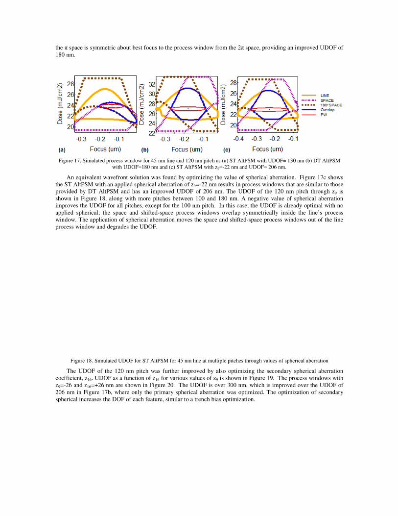
the π space is symmetric about best focus to the
180 nm.
Figure 17. Simulated process window for 45 nm line and 120 nm pitch as
with UDOF=180 nm and (c) ST AltPSM with z
An equivalent wavefront solution was found by optimizing the value of spherical aberration. Figure 17c shows
the ST AltPSM with an applied spherical aberration of z
provided by DT AltPSM and has an improved UDOF of 206 nm. The UDOF of the 120 nm pitch through z
shown in Figure 18, along with more pitches between 100 and 180 nm.
improves the UDOF for all pitches, except for the 100 nm pitch. In this case, the UDOF is already optimal with no
applied spherical; the space and shifted
window. The application of spherical aberration moves the space and shifted
process window and degrades the UDOF.
Figure 18. Simulated UDOF for ST AltPSM for 45 nm line at multiple pitches through values
The UDOF of the 120 nm pitch was further improved by also optimizing the secondary spherical aberration
coefficient, z16. UDOF as a function of z16
z9=-26 and z16=+26 nm are shown in Figure 20. The UDOF is over 300
206 nm in Figure 17b, where only the primary spherical aberration was optimized.
spherical increases the DOF of each feature, similar to a trench bias optimization.
space is symmetric about best focus to the process window from the 2π space, providing an improved UDOF of
process window for 45 nm line and 120 nm pitch as (a) ST AltPSM with UDOF= 130 nm (b) DT AltPSM
with UDOF=180 nm and (c) ST AltPSM with z9=-22 nm and UDOF= 206 nm.
An equivalent wavefront solution was found by optimizing the value of spherical aberration. Figure 17c shows
spherical aberration of z9=-22 nm results in process windows that are similar to those
provided by DT AltPSM and has an improved UDOF of 206 nm. The UDOF of the 120 nm pitch through z
shown in Figure 18, along with more pitches between 100 and 180 nm. A negative value of spherical aberration
improves the UDOF for all pitches, except for the 100 nm pitch. In this case, the UDOF is already optimal with no
applied spherical; the space and shifted-space process windows overlap symmetrically inside the line
window. The application of spherical aberration moves the space and shifted-space process windows out of the line
process window and degrades the UDOF.
Figure 18. Simulated UDOF for ST AltPSM for 45 nm line at multiple pitches through values of spherical aberration
The UDOF of the 120 nm pitch was further improved by also optimizing the secondary spherical aberration
16 for various values of z9 is shown in Figure 19. The process windows with
igure 20. The UDOF is over 300 nm, which is improved over the UDOF of
Figure 17b, where only the primary spherical aberration was optimized. The optimization of secondary
spherical increases the DOF of each feature, similar to a trench bias optimization.
space, providing an improved UDOF of
(a) ST AltPSM with UDOF= 130 nm (b) DT AltPSM
An equivalent wavefront solution was found by optimizing the value of spherical aberration. Figure 17c shows
22 nm results in process windows that are similar to those
provided by DT AltPSM and has an improved UDOF of 206 nm. The UDOF of the 120 nm pitch through z9 is
A negative value of spherical aberration
improves the UDOF for all pitches, except for the 100 nm pitch. In this case, the UDOF is already optimal with no
space process windows overlap symmetrically inside the line’s process
space process windows out of the line
of spherical aberration
The UDOF of the 120 nm pitch was further improved by also optimizing the secondary spherical aberration
is shown in Figure 19. The process windows with
roved over the UDOF of
The optimization of secondary

Figure 19. Simulated UDOF for L45 P120 ST AltPSM
through values of secondary spherical aberration
multiple primary spherical aberration values (z
A simulation with the thick 1% TaSiON AttPSM
nm pitch, is dependent on the pitch. The 70 nm
74 nm, as shown in Figure 22. An optimized value of spherical aberration reduces
to 151 nm, shown in Figure 23. This suggests that spherical aberration provides an equivalent wavefront solution to
match the thick mask with a large ∆BF to a thin mask with a small
Figure 21: Simulated best focus, referenced to
Figure 22. Simulated process windows through pitch for
thick 1% TaSiON AttPSM have 70 nm ∆BF. Useable
of focus is 74 nm.
In this work, pupil wavefront manipulation in the form of spherical aberration was explored to find equivalent
wavefront solutions for thick mask compensation. Experimenta
L45 P120 ST AltPSM
spherical aberration (z16) at
multiple primary spherical aberration values (z9)
Figure 20. Simulated process window for 45 nm line
and 120 nm pitch with z9=-26 nm and z
UDOF of 303 nm
TaSiON AttPSM is shown in Figure 21, where the best focus, referenced to a 90
nm pitch, is dependent on the pitch. The 70 nm ∆BF between the pitch of 84 nm and 135 nm degrades the UDOF to
. An optimized value of spherical aberration reduces the ∆BF and increases the UDOF
. This suggests that spherical aberration provides an equivalent wavefront solution to
BF to a thin mask with a small ∆BF for a specific set of features.
: Simulated best focus, referenced to the 90 nm pitch, for a 1% TaSiON AttPSM with 45 nm line has a
Simulated process windows through pitch for
. Useable depth
Figure 23. Simulated process windows through pitch for
thick 1% TaSiON AttPSM with z9= +15 nm. Useable depth
of focus is 151 nm.
5. CONCLUSIONS
In this work, pupil wavefront manipulation in the form of spherical aberration was explored to find equivalent
mask compensation. Experimental data with a thin mask was carried out in order
process window for 45 nm line
26 nm and z16=+26 nm has a
, where the best focus, referenced to a 90
BF between the pitch of 84 nm and 135 nm degrades the UDOF to
BF and increases the UDOF
. This suggests that spherical aberration provides an equivalent wavefront solution to
BF for a specific set of features.
with 45 nm line has a ∆BF of 70 nm
. Simulated process windows through pitch for
= +15 nm. Useable depth
of focus is 151 nm.
In this work, pupil wavefront manipulation in the form of spherical aberration was explored to find equivalent
l data with a thin mask was carried out in order to

detect spherical aberration’s tendencies. Spherical was shown to linearly shift best focus and to tilt the FEM.
Orientation dependent trends were explained based on the location of the diffraction orders relative to spherical
aberration’s fingerprint. For vertical features imaged with X-Dipole, the best focus shift was pitch dependent,
allowing spherical to tune the through-pitch best focus deviation. A positive value of spherical aberration minimized
the best focus deviation as well as minimized FEM Tilt. Experimental best focus values showed a similar trend to
rigorous simulations, demonstrating that the sensitivity to induced spherical aberration can be predicted.
Rigorous simulations of thick masks suggest that spherical can be used to decrease best focus deviation,
resulting in an improved UDOF. A ST AltPSM can be matched to a DT AltPSM, and likewise, a thick TaSiON
AttPSM can be matched to a thin AttPSM. FlexWave, a high resolution wavefront manipulator on ASML NXT
scanners, has the ability to induce aberrations up to z64, which may allow compensation for more complex thick
mask aberration signatures [20]. This work suggests that pupil manipulation is a powerful tool to compensate for
thick mask effects. However, it does not provide a global solution, only over a specific set of features.
ACKNOWLEDGEMENTS
The authors would like to thank the IMEC lithography department, especially Lieve Van Look and Vicky
Philipsen, as well as Robert Socha of ASML for valuable discussions. The authors would also like to acknowledge
KLA-Tencor for the use of PROLITHTM
and PRODATATM
. This work was supported by the National Science
Foundation through a Graduate Research Fellowship to Monica Kempsell Sears and the Semiconductor Research
Corporation - Global Research Collaboration through Research Task 2126.001.
REFERENCES
[1] R. L. Gordon, C. A. Mack, and J. S. Petersen, “Design and analysis of manufacturable alternating phase-
shifting masks,” Proc. SPIE, 3546, 606-616 (1998).
[2] D. J. Gerold, J. S. Petersen, and D. Levenson, “Multiple pitch transmission and phase analysis of six types
of strong phase-shifting masks,” Proc. SPIE, 4346, 729-743 (2001).
[3] M. D. Levenson, T. Ebihara, and M. Yamachika, “SCAA mask exposures and Phase Phirst designs for 100
nm and below,” Proc. SPIE, 4346, 817-826 (2001).
[4] J. Finders, M. Dusa, P. Nikolsky et al., "Litho and patterning challenges for memory and logic applications
at the 22-nm node." 7640, 76400C-10.
[5] B. W. Smith, [Multi-layered attenuated phase shift mask and a method for making the mask], US Patent
5,939,227 (1999).
[6] V. Philipsen, K. Mesuda, P. De Bisschop et al., “Impact of alternative mask stacks on the imaging
performance at NA 1.20 and above,” Proc. SPIE, 6730, 67301N-12 (2007).
[7] V. Philipsen, P. De Bisschop, and K. Mesuda, “Mask transmission resonance in bi-layer masks,” Proc.
SPIE, 7028, 702815-8 (2008).
[8] A. Erdmann, “Mask modeling in the low k[sub 1] and ultrahigh NA regime: phase and polarization effects,”
Proc. SPIE, 5835, 69-81 (2005).
[9] C. Pierrat, A. K. K. Wong, S. Vaidya et al., “Phase-shifting mask topography effects on lithographic image
quality,” Proc. SPIE, 1927, 28-41 (1993).
[10] A. K. Wong, and A. R. Neureuther, “Mask topography effects in projection printing of phase-shifting
masks,” Electron Devices, IEEE Transactions on, 41(6), 895-902 (1994).
[11] K. Adam, and A. R. Neureuther, “Simplified models for edge transitions in rigorous mask modeling,” Proc.
SPIE, 4346, 331-344 (2001).
[12] M. Cheng, B. C. P. Ho, and D. E. Guenther, “Impact of mask topography and resist effects on optical
proximity correction in advanced alternating phase-shift process,” Proc. SPIE, 5040, 313-326 (2003).
[13] J. Finders, and T. Hollink, “Mask 3D effects: impact on imaging and placement,” Proc. SPIE, 7985,
79850I-23 (2011).
[14] V. N. Mahajan, [Aberration theory made simple] SPIE Optical Engineering Press, Bellingham, Wash., USA
:(1991).
[15] D. G. Flagello, J. de Klerk, G. Davies et al., “Toward a comprehensive control of full-field image quality in
optical photolithography,” Proc. SPIE, 3051, 672-685 (1997).
[16] K. v. I. Schenau, H. Bakker, M. Zellenrath et al., “System qualification and optimization for imaging
performance on the 0.80-NA 248-nm step-and-scan systems,” Proc. SPIE, 4691, 637-651 (2002).

[17] B. W. Smith, [Microlithography: Science and Technology, K. Suzuki and B.W. Smith. eds., Chapter 2
Optics for Photolithography, ] CRC Press, Boca Raton, 191-194 (2007).
[18] M. K. Sears, G. Fenger, J. Mailfert et al., "Extending SMO into the lens pupil domain." 7973, 79731B-9.
[19] L. Van Look, J. Bekaert, K. D'havé et al., “Optical proximity stability control of ArF immersion clusters,”
Proc. SPIE, 7973, 79730R-12 (2011).
[20] F. Staals, A. Andryzhyieuskaya, H. Bakker et al., “Advanced wavefront engineering for improved imaging
and overlay applications on a 1.35 NA immersion scanner,” Proc. SPIE, 7973, 79731G-13 (2011).
Related Documents