Pseudo NMOS Logic Pass-Transistor Logic INEL 4207 - Spring 2011

Welcome message from author
This document is posted to help you gain knowledge. Please leave a comment to let me know what you think about it! Share it to your friends and learn new things together.
Transcript
Pseudo NMOS LogicPass-Transistor Logic
INEL 4207 - Spring 2011
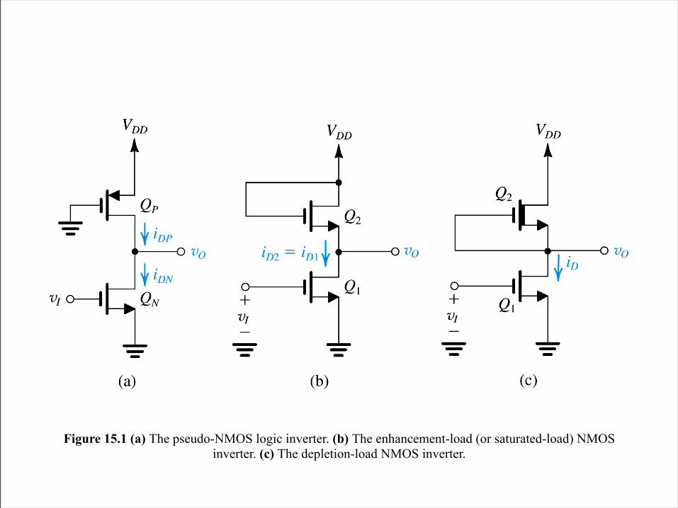
Figure 15.1 (a) The pseudo-NMOS logic inverter. (b) The enhancement-load (or saturated-load) NMOS inverter. (c) The depletion-load NMOS inverter.
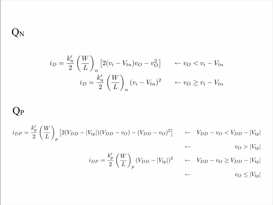
iD =k�
n
2
�W
L
�
n
�2(vi − Vtn)vO − v2
O
�← vO < vi − Vtn
iD =k�
n
2
�W
L
�
n
(vi − Vtn)2 ← vO ≥ vi − Vtn
QN
QP
iDP =k�
p
2
�W
L
�
p
�2(VDD − |Vtp|)(VDD − vO)− (VDD − vO)2
�← VDD − vO < VDD − |Vtp|
← vO > |Vtp|
iDP =k�
p
2
�W
L
�
p
(VDD − |Vtp|)2 ← VDD − vO ≥ VDD − |Vtp|
← vO ≤ |Vtp|
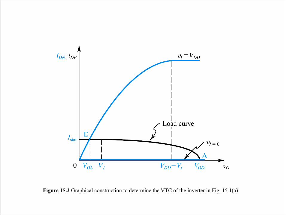
Figure 15.2 Graphical construction to determine the VTC of the inverter in Fig. 15.1(a).
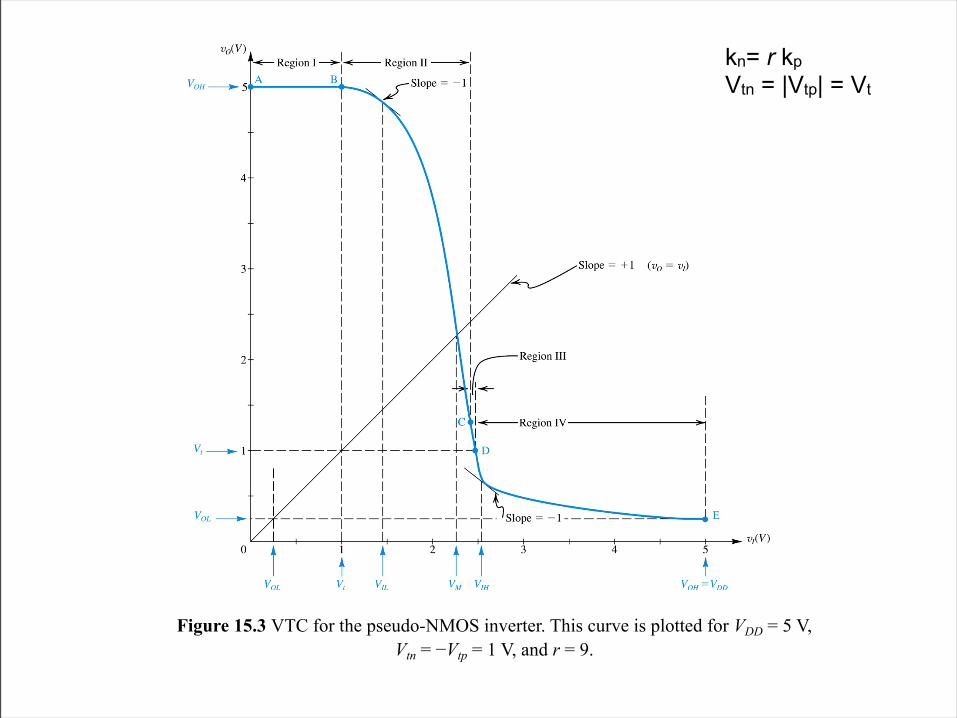
Figure 15.3 VTC for the pseudo-NMOS inverter. This curve is plotted for VDD = 5 V, Vtn = −Vtp = 1 V, and r = 9.
kn= r kpVtn = |Vtp| = Vt
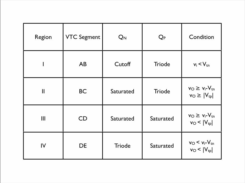
Region VTC Segment QN QP Condition
I AB Cutoff Triode vi < Vtn
II BC Saturated Triode vO ≥ vi-Vtn
vO ≥ |Vtp|
III CD Saturated Saturated vO ≥ vi-Vtn
vO < |Vtp|
IV DE Triode Saturated vO < vi-Vtn
vO < |Vtp|
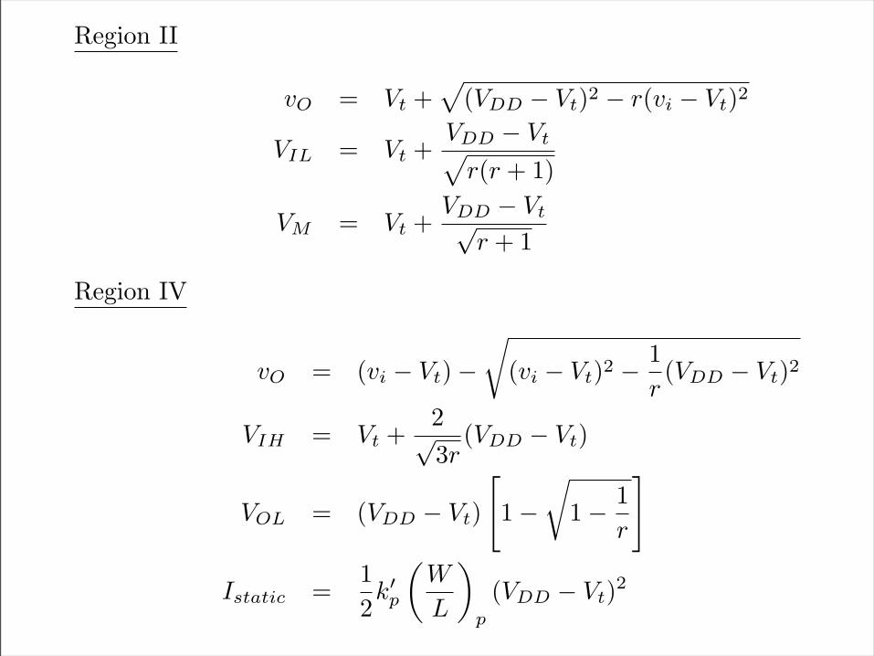
Region II
vO = Vt +�
(VDD − Vt)2 − r(vi − Vt)2
VIL = Vt +VDD − Vt�
r(r + 1)
VM = Vt +VDD − Vt√
r + 1
Region IV
vO = (vi − Vt)−�
(vi − Vt)2 −1r(VDD − Vt)2
VIH = Vt +2√3r
(VDD − Vt)
VOL = (VDD − Vt)
�1−
�1− 1
r
�
Istatic =12k�
p
�W
L
�
p
(VDD − Vt)2
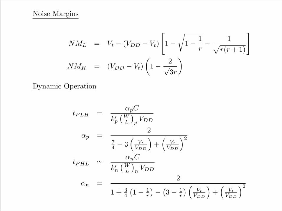
Noise Margins
NML = Vt − (VDD − Vt)
�1−
�1− 1
r− 1�
r(r + 1)
�
NMH = (VDD − Vt)
�1− 2√
3r
�
Dynamic Operation
tPLH =αpC
k�p
�W
L
�pVDD
αp =2
74 − 3
�Vt
VDD
�+
�Vt
VDD
�2
tPHL � αnC
k�n
�W
L
�n
VDD
αn =2
1 +34
�1− 1
r
�−
�3− 1
r
� �Vt
VDD
�+
�Vt
VDD
�2
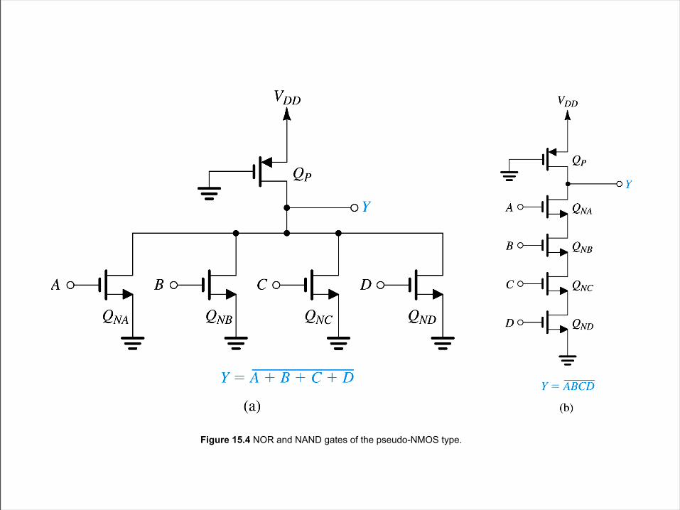
Figure 15.4 NOR and NAND gates of the pseudo-NMOS type.
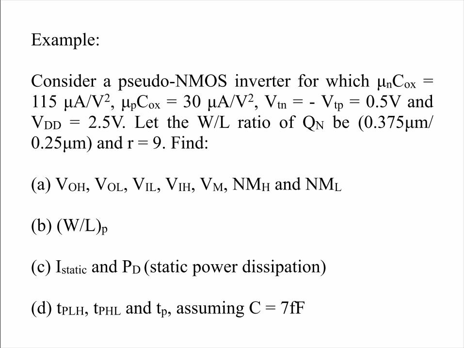
Example:
Consider a pseudo-NMOS inverter for which µnCox = 115 µA/V2, µpCox = 30 µA/V2, Vtn = - Vtp = 0.5V and VDD = 2.5V. Let the W/L ratio of QN be (0.375µm/0.25µm) and r = 9. Find:
(a) VOH, VOL, VIL, VIH, VM, NMH and NML
(b) (W/L)p
(c) Istatic and PD (static power dissipation)
(d) tPLH, tPHL and tp, assuming C = 7fF
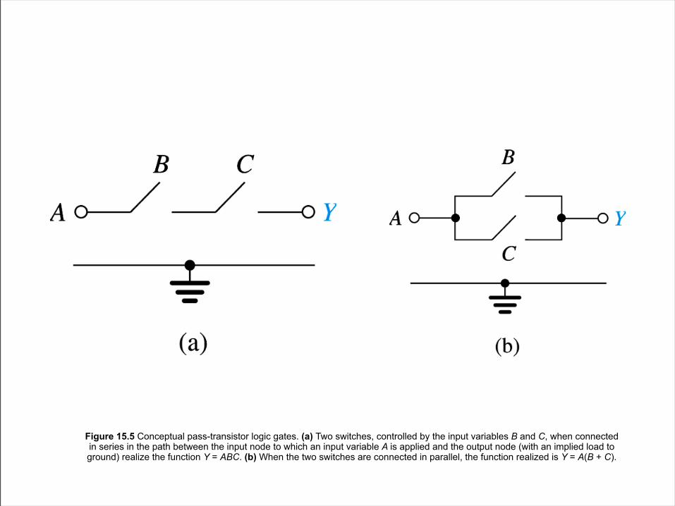
Figure 15.5 Conceptual pass-transistor logic gates. (a) Two switches, controlled by the input variables B and C, when connected in series in the path between the input node to which an input variable A is applied and the output node (with an implied load to ground) realize the function Y = ABC. (b) When the two switches are connected in parallel, the function realized is Y = A(B + C).
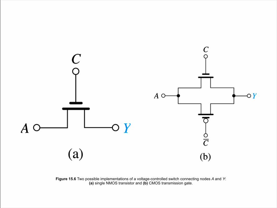
Figure 15.6 Two possible implementations of a voltage-controlled switch connecting nodes A and Y: (a) single NMOS transistor and (b) CMOS transmission gate.
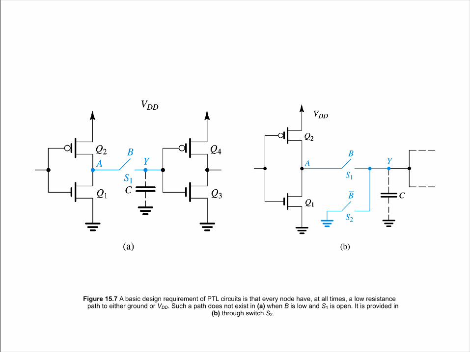
Figure 15.7 A basic design requirement of PTL circuits is that every node have, at all times, a low resistancepath to either ground or VDD. Such a path does not exist in (a) when B is low and S1 is open. It is provided in
(b) through switch S2.
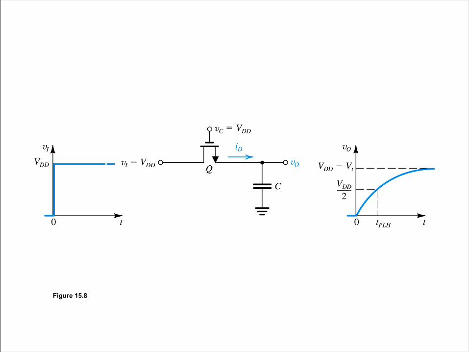
Figure 15.8
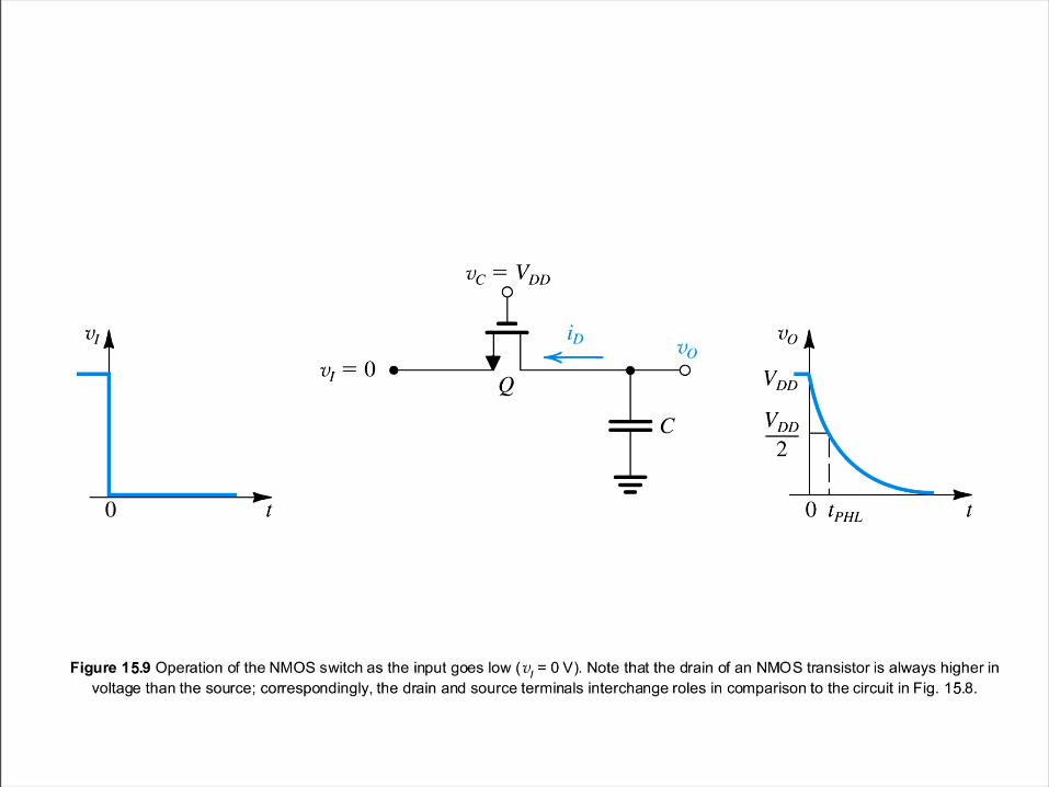
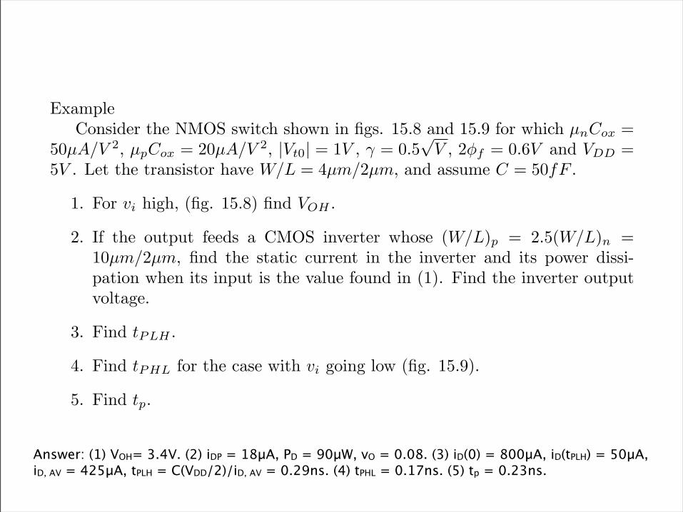
Example
Consider the NMOS switch shown in figs. 15.8 and 15.9 for which µnCox =
50µA/V 2, µpCox = 20µA/V 2, |Vt0| = 1V , γ = 0.5√
V , 2φf = 0.6V and VDD =
5V . Let the transistor have W/L = 4µm/2µm, and assume C = 50fF .
1. For vi high, (fig. 15.8) find VOH .
2. If the output feeds a CMOS inverter whose (W/L)p = 2.5(W/L)n =
10µm/2µm, find the static current in the inverter and its power dissi-
pation when its input is the value found in (1). Find the inverter output
voltage.
3. Find tPLH .
4. Find tPHL for the case with vi going low (fig. 15.9).
5. Find tp.
Answer: (1) VOH= 3.4V. (2) iDP = 18μA, PD = 90μW, vO = 0.08. (3) iD(0) = 800μA, iD(tPLH) = 50μA, iD, AV = 425μA, tPLH = C(VDD/2)/iD, AV = 0.29ns. (4) tPHL = 0.17ns. (5) tp = 0.23ns.
Related Documents


![CHAPTER 12 ARRAY SUBSYSTEMS [12.4-12.9]web.cecs.pdx.edu/~chiang/ECE_426_526_Summer_2011/Manjari_S... · Pseudo-nMOS ROM ... FULL and EMPTY flags ... First In First Out [FIFO] –](https://static.cupdf.com/doc/110x72/5ab549917f8b9a6e1c8ca011/chapter-12-array-subsystems-124-129webcecspdxeduchiangece426526summer2011manjarispseudo-nmos.jpg)