PROGRAMMABLE PERIPHERAL INTERFACE -8255 Features: • It is a programmable device. • It has 24 I/O programmable pins. T T L compatible. Improved dc driving capability

PROGRAMMABLE PERIPHERAL INTERFACE -8255 Features: It is a programmable device. It has 24 I/O programmable pins. T T L compatible. Improved dc driving.
Dec 14, 2015
Welcome message from author
This document is posted to help you gain knowledge. Please leave a comment to let me know what you think about it! Share it to your friends and learn new things together.
Transcript
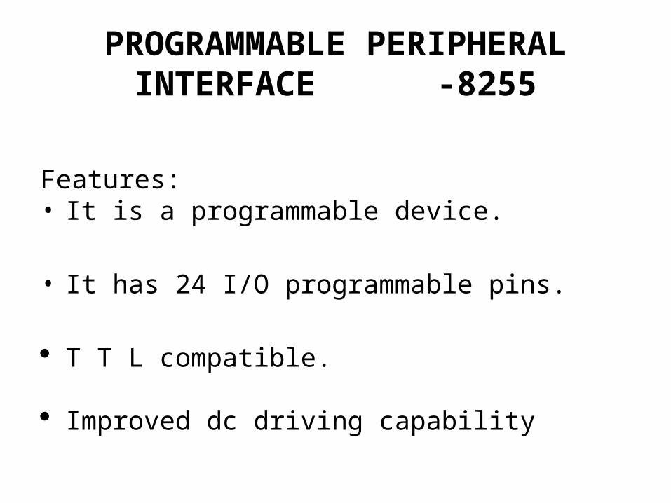
PROGRAMMABLE PERIPHERAL INTERFACE -8255
Features:• It is a programmable device.
• It has 24 I/O programmable pins.
T T L compatible.
Improved dc driving capability
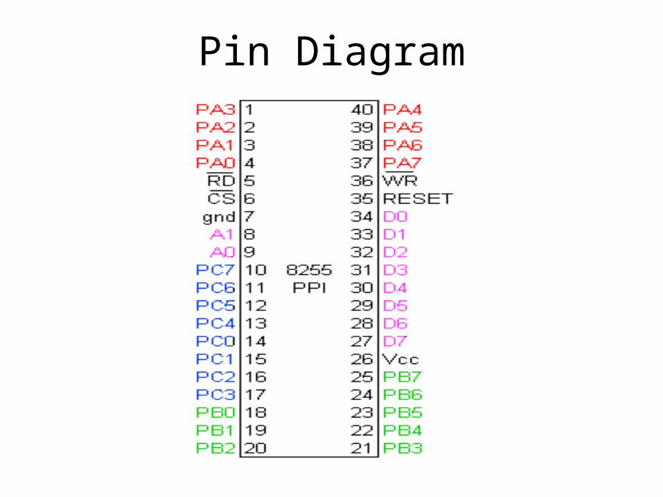
Pin Diagram
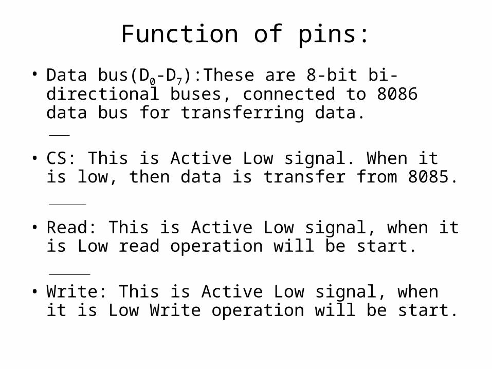
Function of pins:
• Data bus(D0-D7):These are 8-bit bi-directional buses, connected to 8086 data bus for transferring data.
• CS: This is Active Low signal. When it is low, then data is transfer from 8085.
• Read: This is Active Low signal, when it is Low read operation will be start.
• Write: This is Active Low signal, when it is Low Write operation will be start.
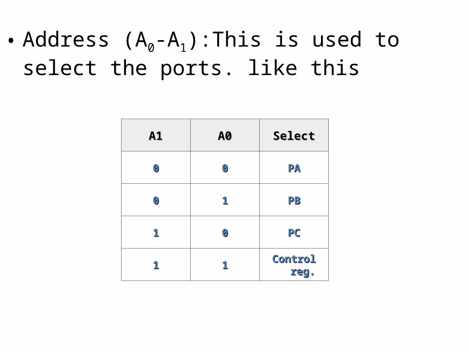
A1A1 A0A0 SelectSelect
00 00 PAPA
00 11 PBPB
11 00 PCPC
11 11Control Control
reg.reg.
• Address (A0-A1):This is used to select the ports. like this
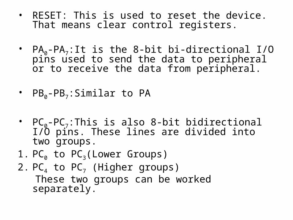
• RESET: This is used to reset the device. That means clear control registers.
• PA0-PA7:It is the 8-bit bi-directional I/O pins used to send the data to peripheral or to receive the data from peripheral.
• PB0-PB7:Similar to PA
• PC0-PC7:This is also 8-bit bidirectional I/O pins. These lines are divided into two groups.
1. PC0 to PC3(Lower Groups)2. PC4 to PC7 (Higher groups) These two groups can be worked separately.
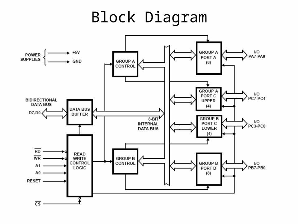
Block Diagram
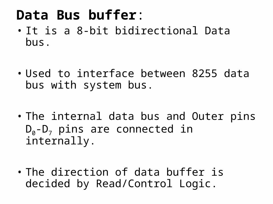
Data Bus buffer:• It is a 8-bit bidirectional Data bus.
• Used to interface between 8255 data bus with system bus.
• The internal data bus and Outer pins D0-D7 pins are connected in internally.
• The direction of data buffer is decided by Read/Control Logic.
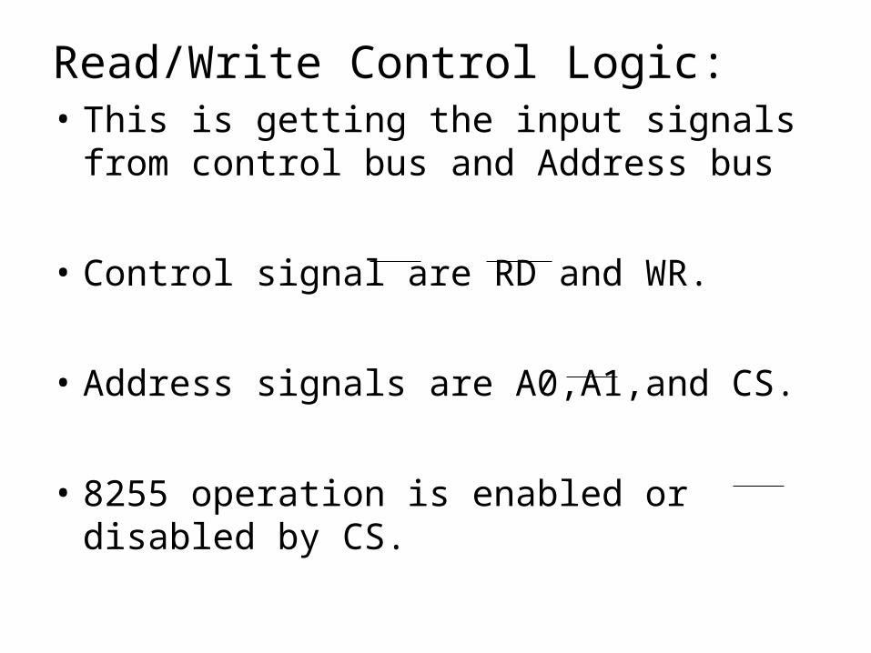
Read/Write Control Logic:• This is getting the input signals from control
bus and Address bus
• Control signal are RD and WR.
• Address signals are A0,A1,and CS.
• 8255 operation is enabled or disabled by CS.
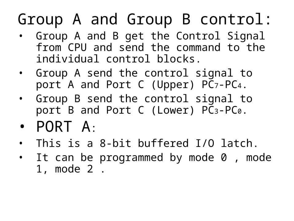
Group A and Group B control:• Group A and B get the Control Signal from CPU and
send the command to the individual control blocks. • Group A send the control signal to port A and Port
C (Upper) PC7-PC4.• Group B send the control signal to port B and Port
C (Lower) PC3-PC0.
• PORT A:• This is a 8-bit buffered I/O latch.• It can be programmed by mode 0 , mode 1, mode 2
.
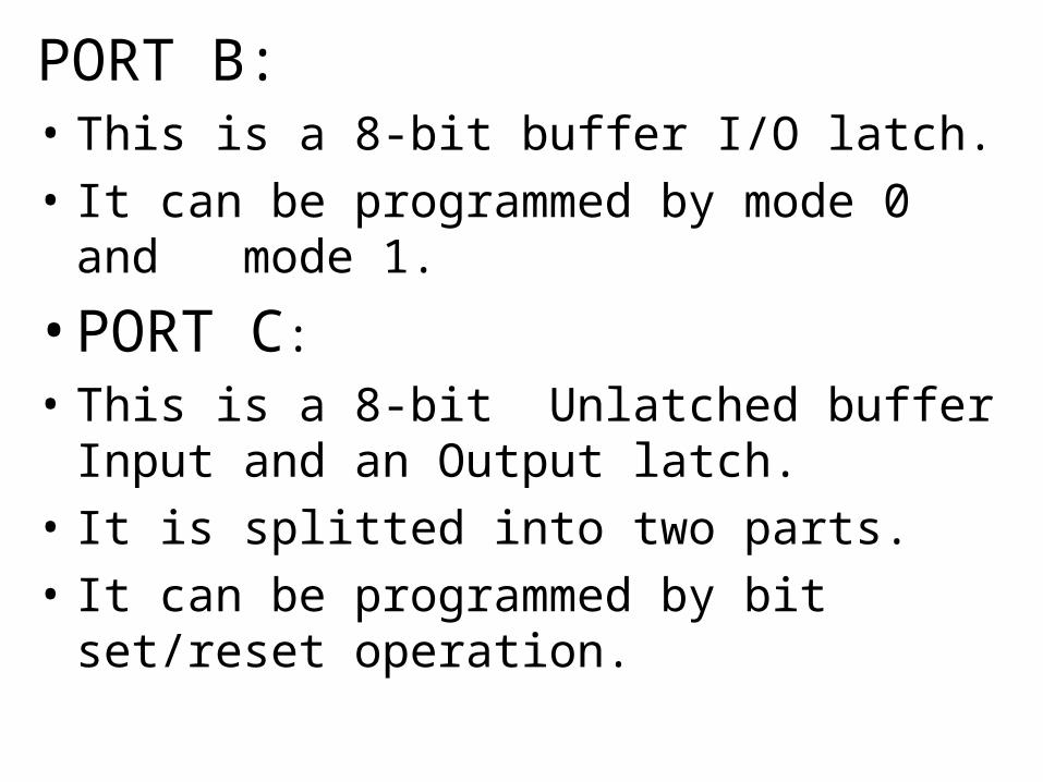
PORT B:• This is a 8-bit buffer I/O latch.• It can be programmed by mode 0 and mode 1.
• PORT C:• This is a 8-bit Unlatched buffer Input and an
Output latch.• It is splitted into two parts.• It can be programmed by bit set/reset operation.
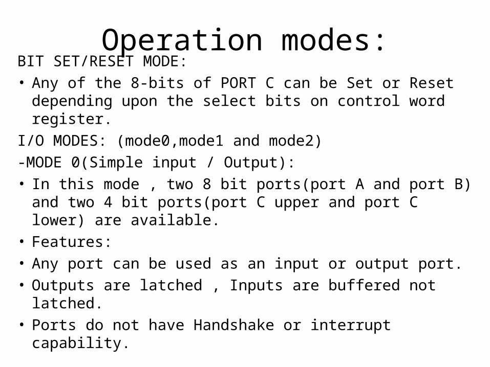
Operation modes:BIT SET/RESET MODE:• Any of the 8-bits of PORT C can be Set or Reset
depending upon the select bits on control word register.I/O MODES: (mode0,mode1 and mode2)-MODE 0(Simple input / Output):• In this mode , two 8 bit ports(port A and port B) and two
4 bit ports(port C upper and port C lower) are available.• Features:• Any port can be used as an input or output port.• Outputs are latched , Inputs are buffered not latched.• Ports do not have Handshake or interrupt capability.
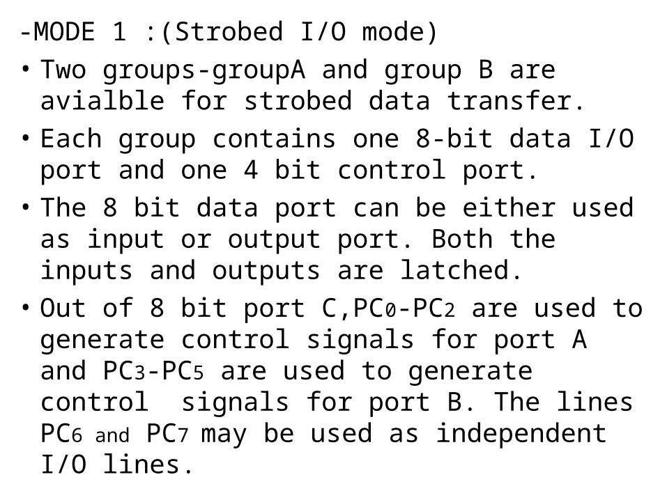
-MODE 1 :(Strobed I/O mode)• Two groups-groupA and group B are avialble for
strobed data transfer.• Each group contains one 8-bit data I/O port and
one 4 bit control port.• The 8 bit data port can be either used as input or
output port. Both the inputs and outputs are latched.
• Out of 8 bit port C,PC0-PC2 are used to generate control signals for port A and PC3-PC5 are used to generate control signals for port B. The lines PC6
and PC7 may be used as independent I/O lines.
MODE 2: Strobed bi-directional I/O mode:• This mode allows bidirectional data transfer over a single
8-bit data bus (port A) using handshake signals.• Port A is working as 8-bit bidirectional.• 5 bit control port PC3-PC7 is used for
generating/accepting handshaking signals of port A.• Both the inputs and outputs are latched.• Here, port B and three lines of port C (PC2-PC0) may be
used in either simple I/O mode or strobed mode.
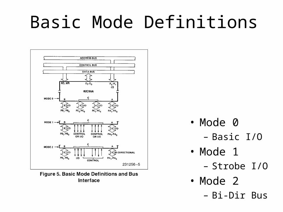
Basic Mode Definitions
• Mode 0– Basic I/O
• Mode 1– Strobe I/O
• Mode 2– Bi-Dir Bus
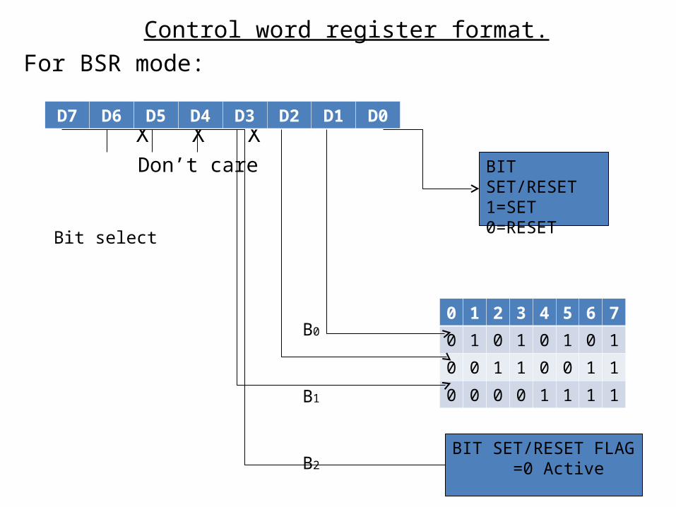
Control word register format.For BSR mode:
X X X Don’t care
Bit select B0
B1
B2
D7 D6 D5 D4 D3 D2 D1 D0
0 1 2 3 4 5 6 7
0 1 0 1 0 1 0 1
0 0 1 1 0 0 1 1
0 0 0 0 1 1 1 1
BIT SET/RESET1=SET0=RESET
BIT SET/RESET FLAG =0 Active
• PC0-PC7 is set or reset as per the status of D0.
• A BSR word is written for each bit• Example:• PC3 is Set then control register will be 0XXX0111.• PC4 is Reset then control register will be
0XXX01000.• X is a don’t care.
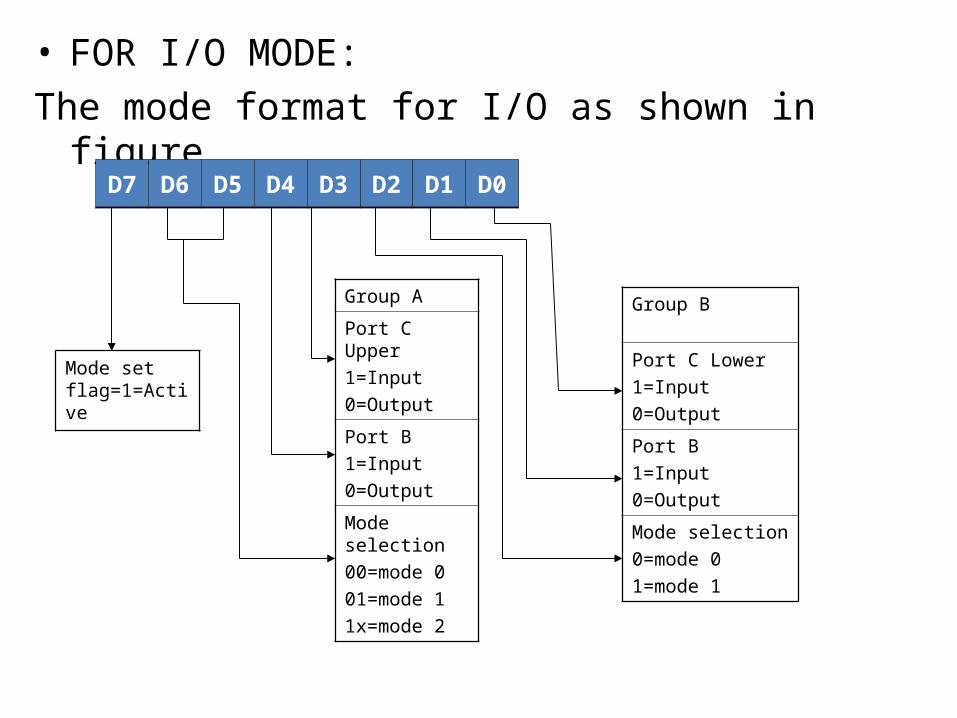
• FOR I/O MODE:The mode format for I/O as shown in figure
D7
D6
D5
D4
D3
D2
D1
D0
Group A
Port C Upper 1=Input0=Output
Port B 1=Input0=Output
Mode selection00=mode 001=mode 11x=mode 2
Group B
Port C Lower 1=Input0=Output
Port B 1=Input0=Output
Mode selection0=mode 01=mode 1
Mode set flag=1=Active
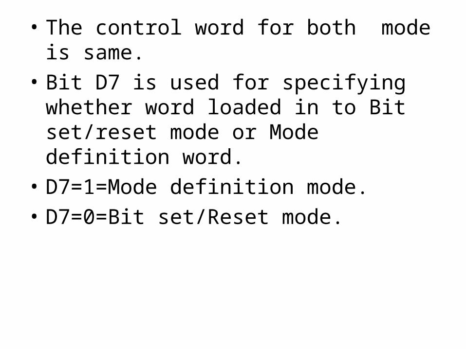
• The control word for both mode is same.• Bit D7 is used for specifying whether word
loaded in to Bit set/reset mode or Mode definition word.
• D7=1=Mode definition mode.• D7=0=Bit set/Reset mode.
Related Documents