Semiconductor Radiation Engineering- Global Applications & Trends Prof. Dr. Ahmed Shuja Syed Member Experts Group, SASSI Vice President, CESET Adjunct Professor & Principal Investigator Advanced Electronics Laboratory Project, Faculty of Engineering & Technology, International Islamic University, Islamabad Centre for Emerging Sciences, Engineering & Technology (CESET), Islamabad

Prof. Dr. Ahmed Shuja Syed Member Experts Group, SASSI Vice President, CESET Adjunct Professor & Principal Investigator Advanced Electronics Laboratory.
Dec 15, 2015
Welcome message from author
This document is posted to help you gain knowledge. Please leave a comment to let me know what you think about it! Share it to your friends and learn new things together.
Transcript
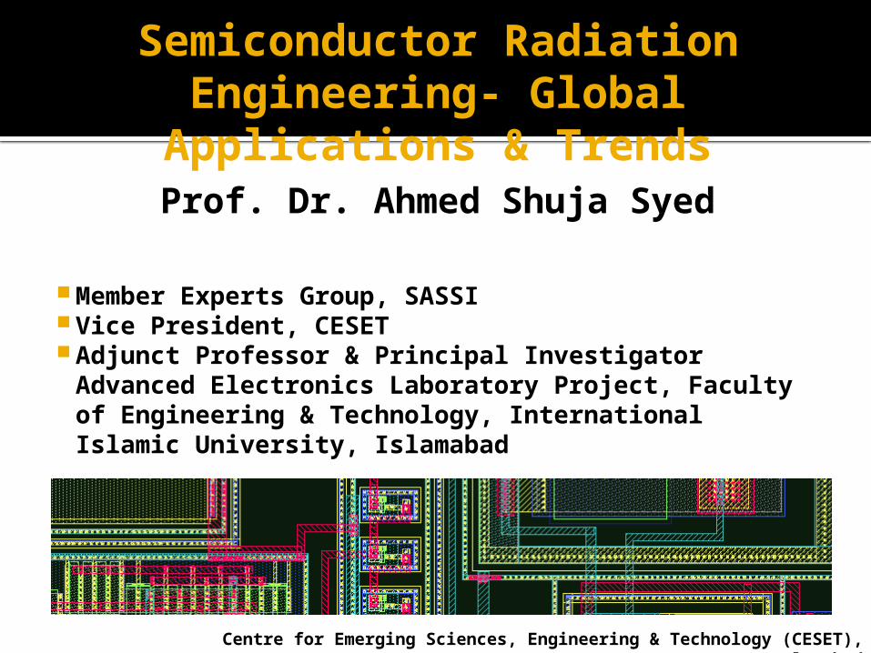
Semiconductor Radiation Engineering- Global
Applications & TrendsProf. Dr. Ahmed Shuja Syed
Member Experts Group, SASSI Vice President, CESET Adjunct Professor & Principal Investigator
Advanced Electronics Laboratory Project, Faculty of Engineering & Technology, International Islamic University, Islamabad
Centre for Emerging Sciences, Engineering & Technology (CESET), Islamabad
Semiconductor Radiation Engineering- Global
Applications & Trends
Centre for Emerging Sciences, Engineering & Technology (CESET), Islamabad
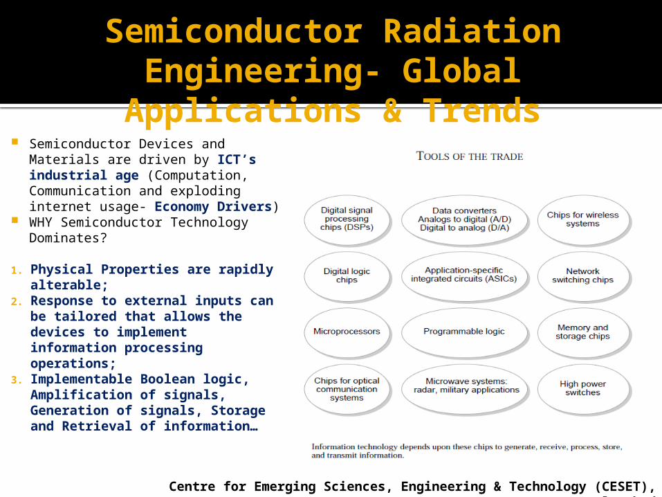
Semiconductor Devices and Materials are driven by ICT’s industrial age (Computation, Communication and exploding internet usage- Economy Drivers)
WHY Semiconductor Technology Dominates?
1. Physical Properties are rapidly alterable;
2. Response to external inputs can be tailored that allows the devices to implement information processing operations;
3. Implementable Boolean logic, Amplification of signals, Generation of signals, Storage and Retrieval of information…
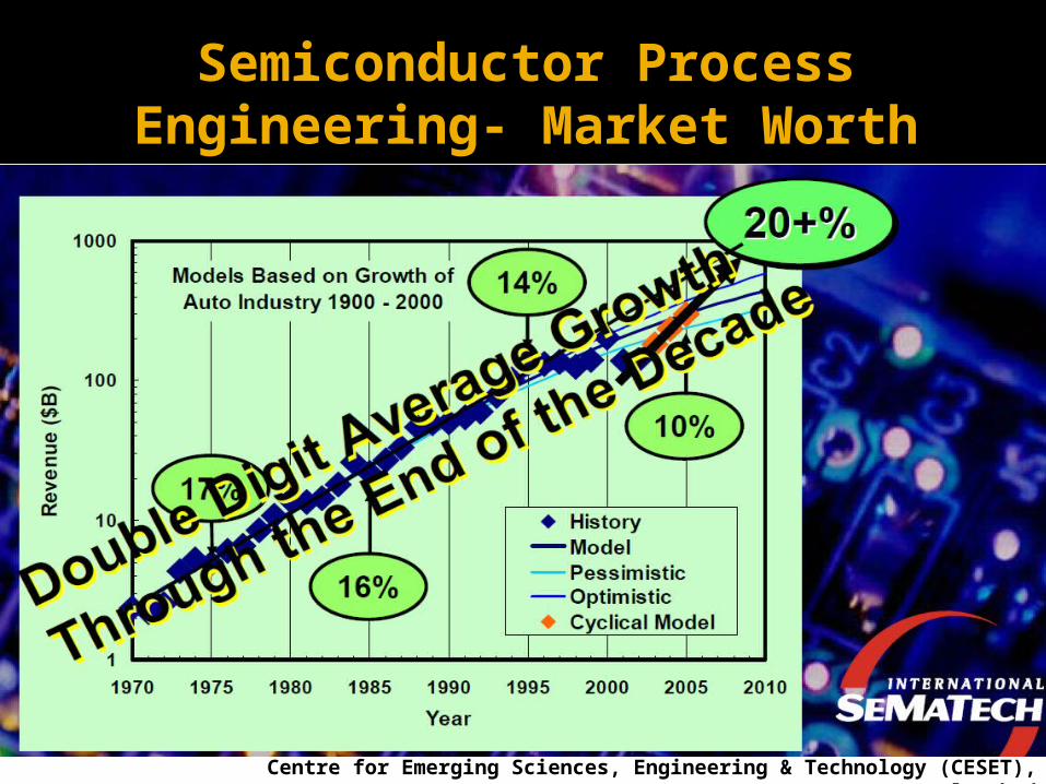
Semiconductor Process Engineering- Market Worth
Centre for Emerging Sciences, Engineering & Technology (CESET), Islamabad
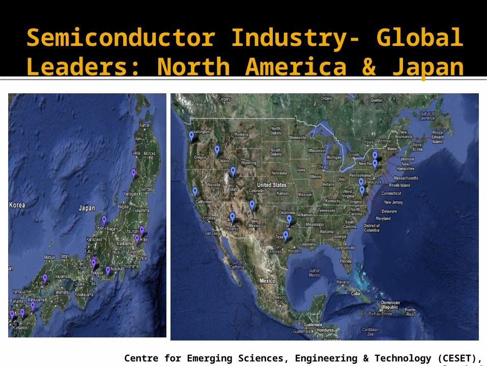
Semiconductor Industry- Global Leaders: North America & Japan
Centre for Emerging Sciences, Engineering & Technology (CESET), Islamabad
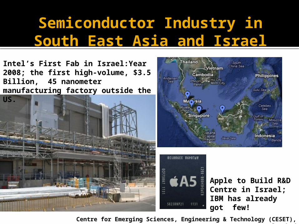
Semiconductor Industry in South East Asia and Israel
Centre for Emerging Sciences, Engineering & Technology (CESET), Islamabad
Intel’s First Fab in Israel:Year 2008; the first high-volume, $3.5 Billion, 45 nanometer manufacturing factory outside the US.
Apple to Build R&D Centre in Israel; IBM has already got few!
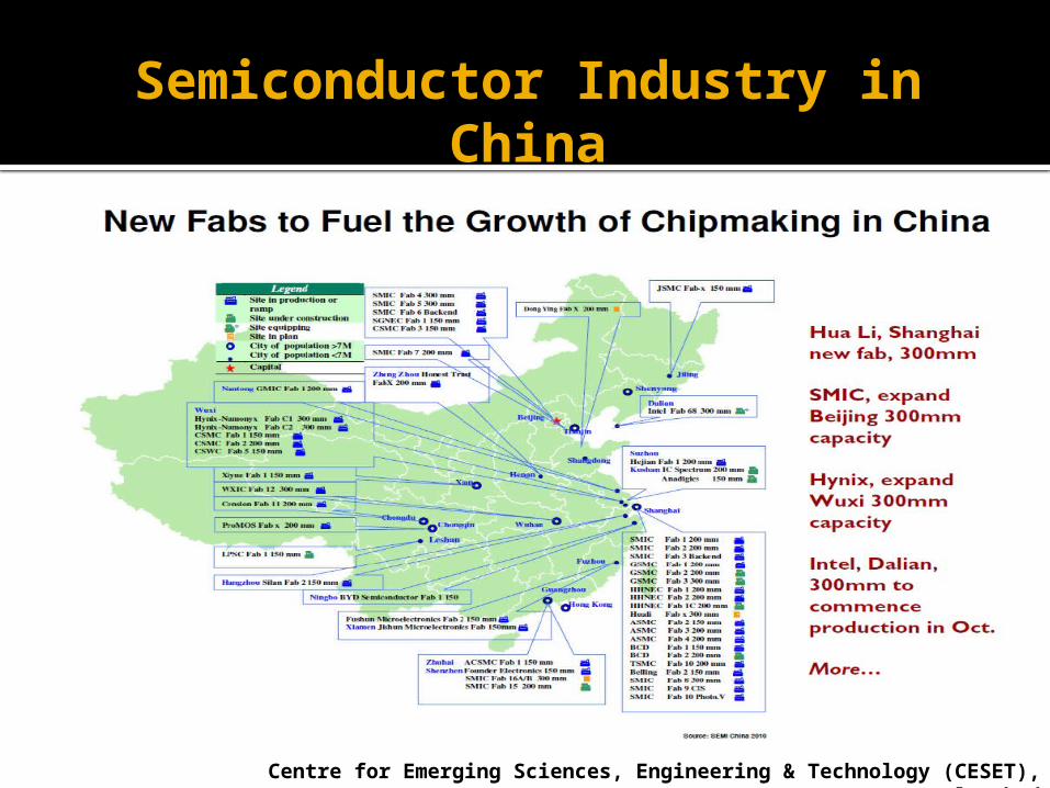
Semiconductor Industry in China
Centre for Emerging Sciences, Engineering & Technology (CESET), Islamabad
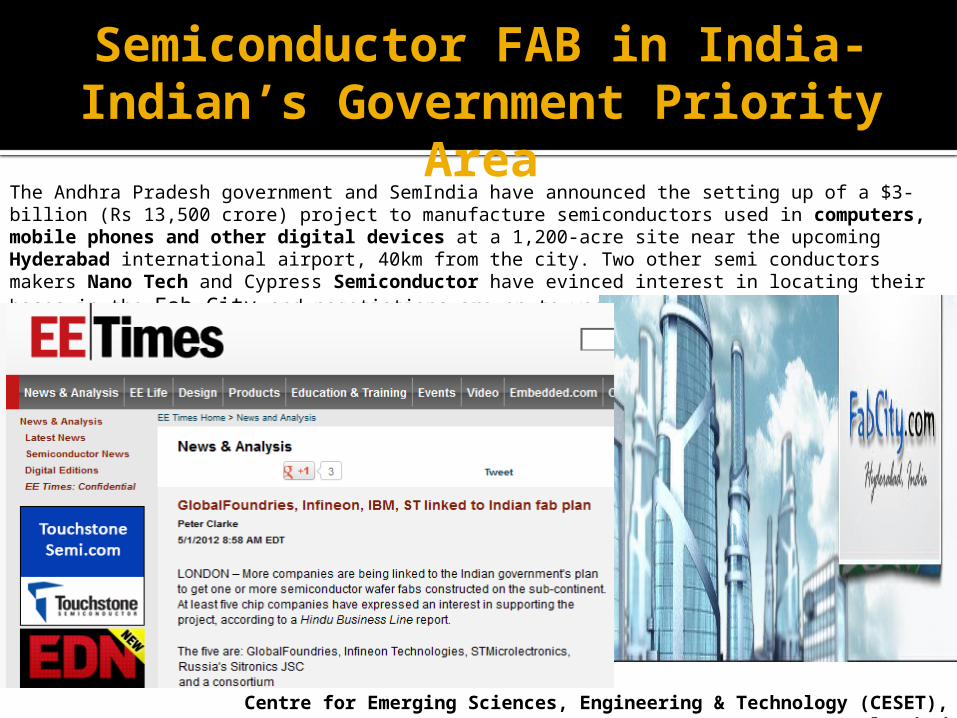
Semiconductor FAB in India- Indian’s Government Priority
Area
Centre for Emerging Sciences, Engineering & Technology (CESET), Islamabad
The Andhra Pradesh government and SemIndia have announced the setting up of a $3-billion (Rs 13,500 crore) project to manufacture semiconductors used in computers, mobile phones and other digital devices at a 1,200-acre site near the upcoming Hyderabad international airport, 40km from the city. Two other semi conductors makers Nano Tech and Cypress Semiconductor have evinced interest in locating their bases in the Fab City and negotiations are on to woo some more semiconductor companies. Chennai, Bangalore and Hyderabad, have been hotly pursuing the project.
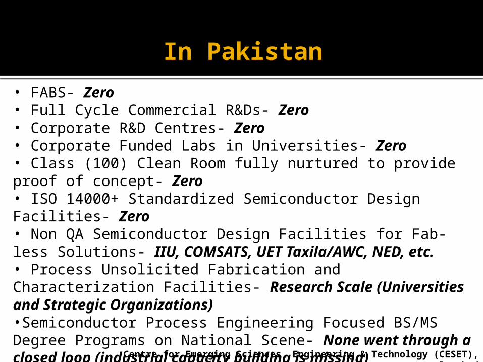
In Pakistan
Centre for Emerging Sciences, Engineering & Technology (CESET), Islamabad
• FABS- Zero• Full Cycle Commercial R&Ds- Zero• Corporate R&D Centres- Zero• Corporate Funded Labs in Universities- Zero• Class (100) Clean Room fully nurtured to provide proof of concept- Zero• ISO 14000+ Standardized Semiconductor Design Facilities- Zero• Non QA Semiconductor Design Facilities for Fab-less Solutions- IIU, COMSATS, UET Taxila/AWC, NED, etc.• Process Unsolicited Fabrication and Characterization Facilities- Research Scale (Universities and Strategic Organizations)•Semiconductor Process Engineering Focused BS/MS Degree Programs on National Scene- None went through a closed loop (industrial capacity building is missing)

Lets Compare it with UAE Only in 2011-12 Alone!
Centre for Emerging Sciences, Engineering & Technology (CESET), Islamabad
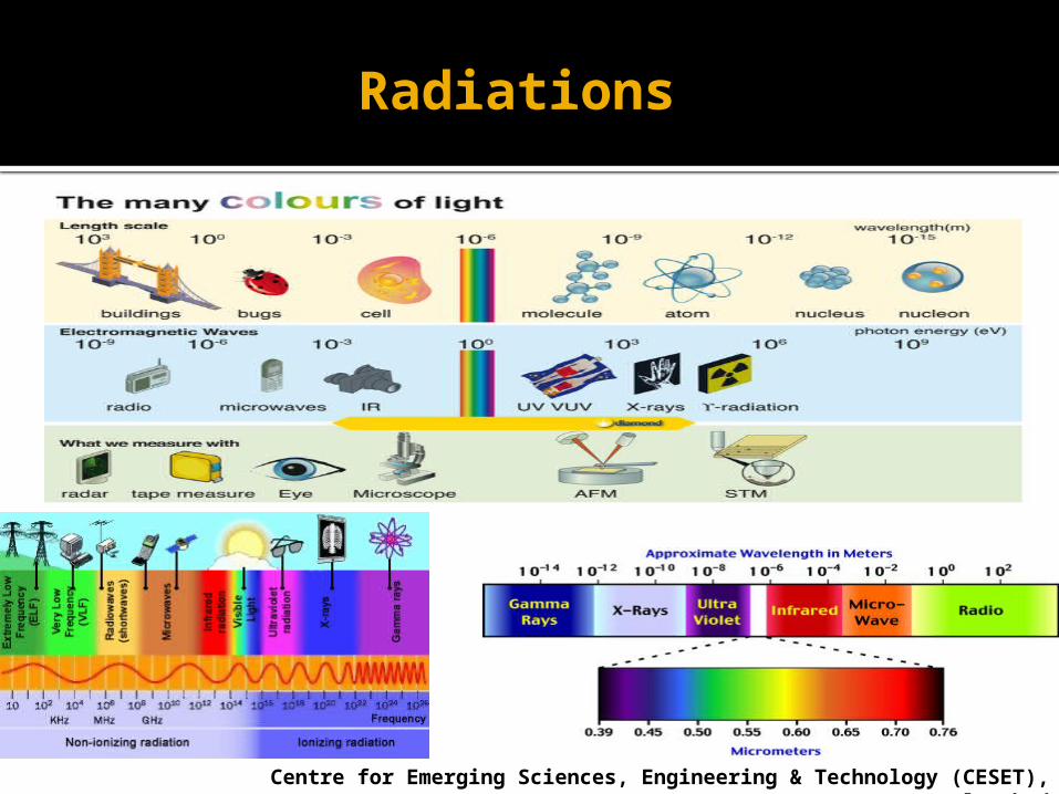
Radiations
Centre for Emerging Sciences, Engineering & Technology (CESET), Islamabad
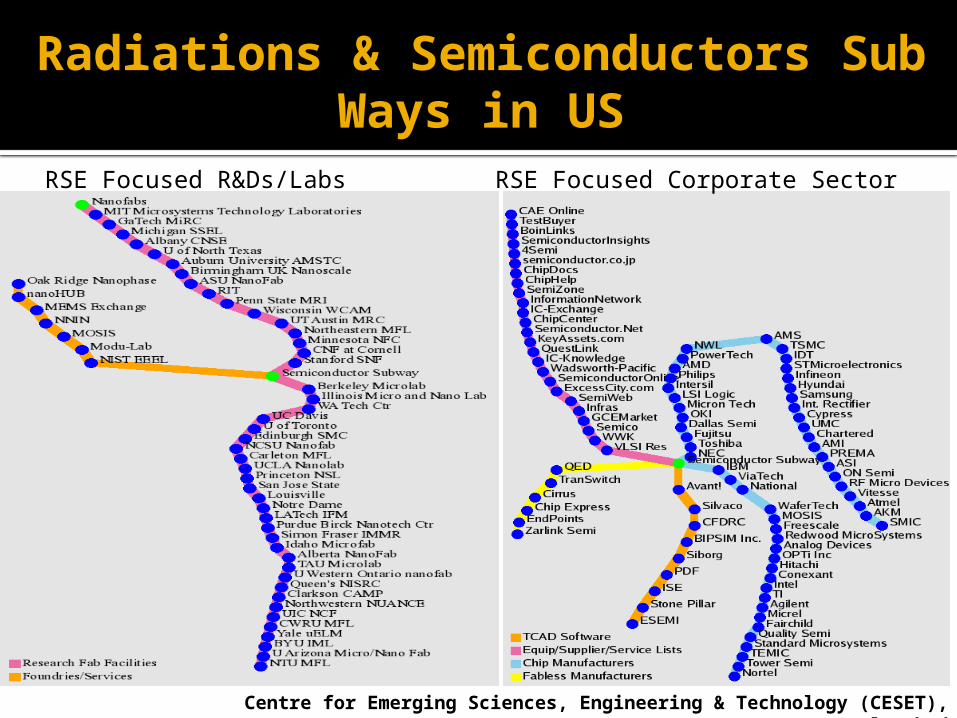
Radiations & Semiconductors Sub Ways in US
Centre for Emerging Sciences, Engineering & Technology (CESET), Islamabad
RSE Focused R&Ds/Labs RSE Focused Corporate Sector
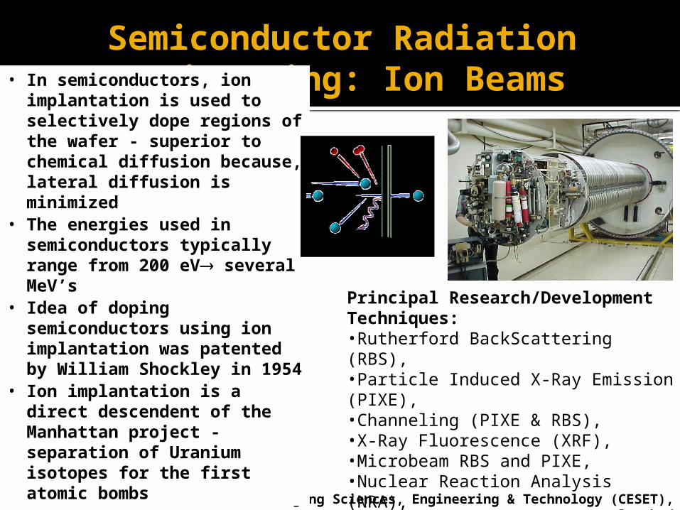
Semiconductor Radiation Engineering: Ion Beams
Centre for Emerging Sciences, Engineering & Technology (CESET), Islamabad
Principal Research/Development Techniques: •Rutherford BackScattering (RBS), •Particle Induced X-Ray Emission (PIXE), •Channeling (PIXE & RBS),•X-Ray Fluorescence (XRF),•Microbeam RBS and PIXE,•Nuclear Reaction Analysis (NRA),•Ion Implantation, and•Optical and electrical characterization
• In semiconductors, ion implantation is used to selectively dope regions of the wafer - superior to chemical diffusion because, lateral diffusion is minimized
• The energies used in semiconductors typically range from 200 eV several MeV’s
• Idea of doping semiconductors using ion implantation was patented by William Shockley in 1954
• Ion implantation is a direct descendent of the Manhattan project - separation of Uranium isotopes for the first atomic bombs
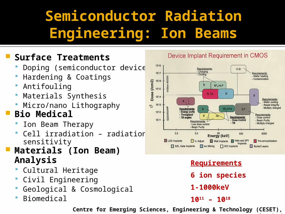
Semiconductor Radiation Engineering: Ion Beams
Centre for Emerging Sciences, Engineering & Technology (CESET), Islamabad
Surface Treatments Doping (semiconductor devices) Hardening & Coatings Antifouling Materials Synthesis Micro/nano Lithography
Bio Medical Ion Beam Therapy Cell irradiation – radiation sensitivity
Materials (Ion Beam) Analysis Cultural Heritage Civil Engineering Geological & Cosmological Biomedical
Requirements
6 ion species
1-1000keV
1011 – 1018
Semiconductor Radiation Engineering: Ion Beams
Centre for Emerging Sciences, Engineering & Technology (CESET), Islamabad
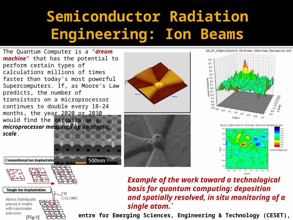
Example of the work toward a technological basis for quantum computing: deposition and spatially resolved, in situ monitoring of a single atom.`
The Quantum Computer is a "dream machine" that has the potential to perform certain types of calculations millions of times faster than today's most powerful Supercomputers. If, as Moore's Law predicts, the number of transistors on a microprocessor continues to double every 18-24 months, the year 2020 or 2030 would find the circuits on a microprocessor measured on an atomic scale.
Semiconductor Radiation Engineering- Light Source
Irradiation
Centre for Emerging Sciences, Engineering & Technology (CESET), Islamabad
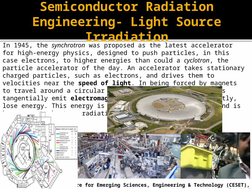
In 1945, the synchrotron was proposed as the latest accelerator for high-energy physics, designed to push particles, in this case electrons, to higher energies than could a cyclotron, the particle accelerator of the day. An accelerator takes stationary charged particles, such as electrons, and drives them to velocities near the speed of light. In being forced by magnets to travel around a circular storage ring, charged particles tangentially emit electromagnetic radiation and, consequently, lose energy. This energy is emitted in the form of light and is known as synchrotron radiation.
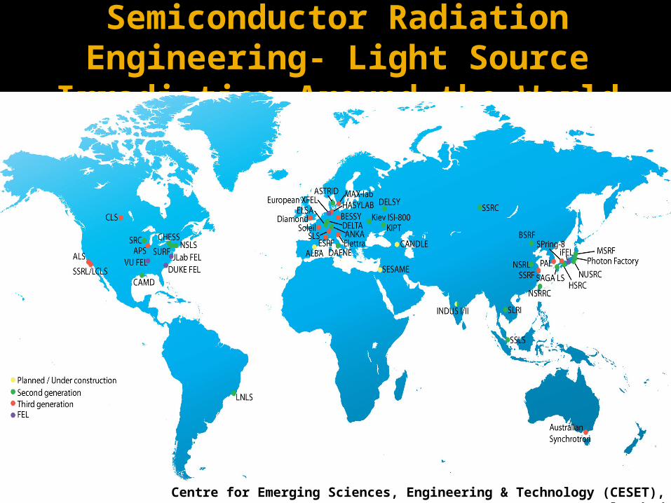
Semiconductor Radiation Engineering- Light Source
Irradiation Around the World
Centre for Emerging Sciences, Engineering & Technology (CESET), Islamabad
Semiconductor Radiation Engineering- Light Source
Irradiation In Pakistan’s Vicinity
Centre for Emerging Sciences, Engineering & Technology (CESET), Islamabad
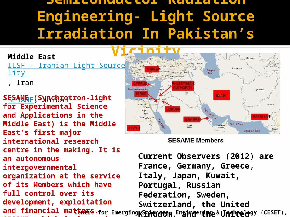
Middle East ILSF - Iranian Light Source Facility , Iran SESAME, Jordan
Current Observers (2012) are France, Germany, Greece, Italy, Japan, Kuwait, Portugal, Russian Federation, Sweden, Switzerland, the United Kingdom, and the United States of America.
SESAME (Synchrotron-light for Experimental Science and Applications in the Middle East) is the Middle East's first major international research centre in the making. It is an autonomous intergovernmental organization at the service of its Members which have full control over its development, exploitation and financial matters. SESAME, which is located at Allan (Jordan), will be a "third generation" synchrotron light source.
Focused Synchrotron Applications to Semiconductor
Design/Process/Fabrication
Centre for Emerging Sciences, Engineering & Technology (CESET), Islamabad
Facilities are used for the detailed study of engineering and manufacturing. The X-ray beams allow for detailed analysis and modeling of strain, cracks and corrosion as well as in situ study of materials during production processing. This research is vital to the development of high performance materials and their use in innovative products and structures.Determining the properties and morphology of buried layers and interfaces remains an important area in solid-state science. Many of the technological products of materials science are based on thin-film devices, which consist of a series of such layers. Structural studies of in-situ processing of semiconducting polymer films is also likely to be an important area of growth in the coming decade.
Diffraction of high-intensity x-ray beams is an ideal technique to study spin, charge and orbital ordering in single crystal samples to understand high temperature superconductivity.Magnetic contrast in images will be provided by exploiting either circular or linear dichroism. At 10 nm resolution, the nanoscience beamline provides high quality images of the magnetic domains of thin films and multilayers, clusters, exchange-biased films, giant magnetoresistive metals and metal-semiconductor spintronic materials. At higher spatial resolutions it is possible to conduct experiments on individual nanoclusters. Spectroscopy on nanosized particles is able to unravel their electronic and chemical properties which may be dominated by the surface due to a large surface to volume ratio.
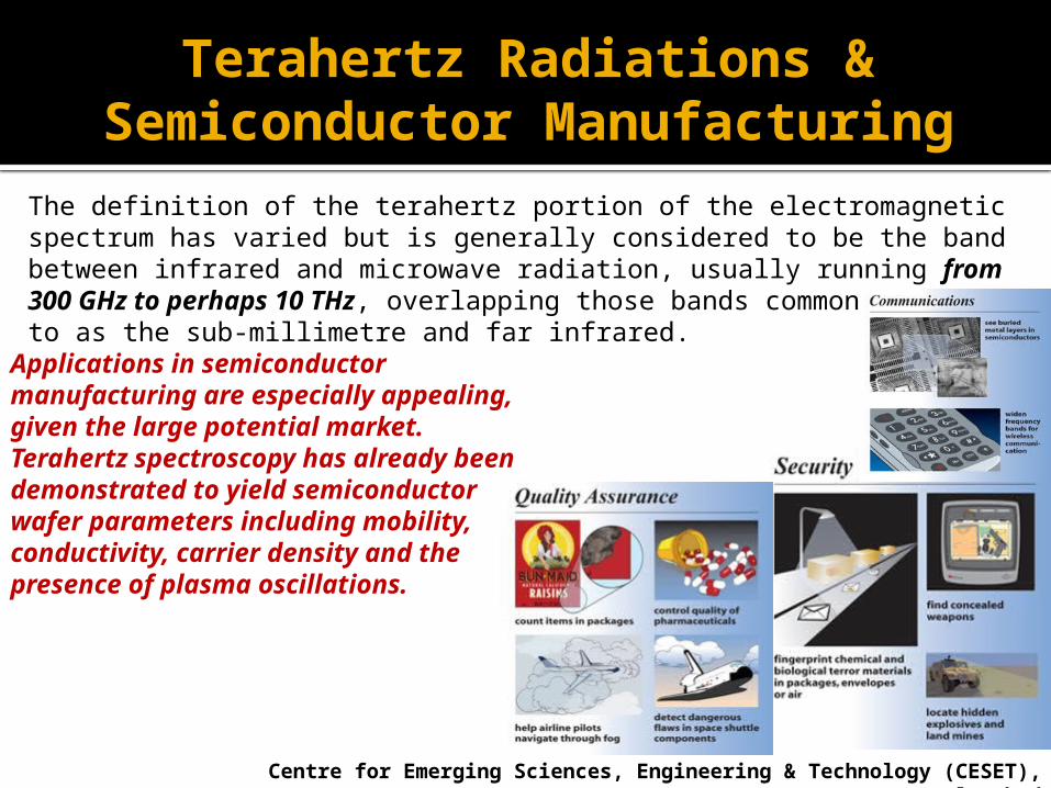
Terahertz Radiations & Semiconductor Manufacturing
Centre for Emerging Sciences, Engineering & Technology (CESET), Islamabad
The definition of the terahertz portion of the electromagnetic spectrum has varied but is generally considered to be the band between infrared and microwave radiation, usually running from 300 GHz to perhaps 10 THz, overlapping those bands commonly referred to as the sub-millimetre and far infrared.
Applications in semiconductor manufacturing are especially appealing, given the large potential market. Terahertz spectroscopy has already been demonstrated to yield semiconductor wafer parameters including mobility, conductivity, carrier density and the presence of plasma oscillations.
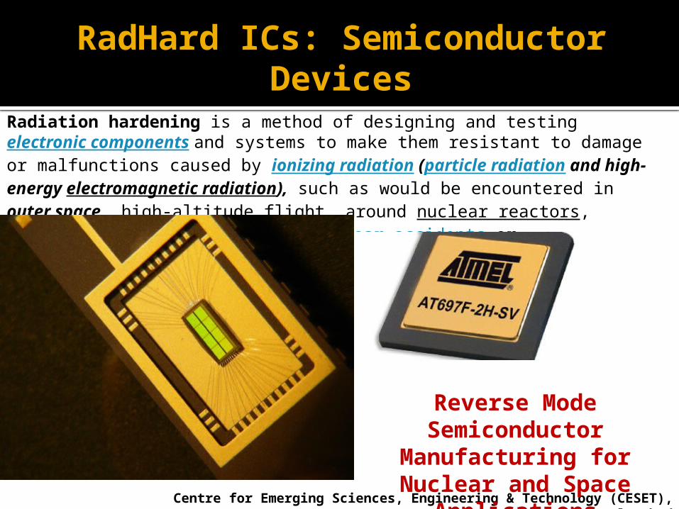
RadHard ICs: Semiconductor Devices
Centre for Emerging Sciences, Engineering & Technology (CESET), Islamabad
Radiation hardening is a method of designing and testing electronic components and systems to make them resistant to damage or malfunctions caused by ionizing radiation (particle radiation and high-energy electromagnetic radiation), such as would be encountered in outer space, high-altitude flight, around nuclear reactors, particle accelerators, during nuclear accidents or nuclear warfare.
Reverse Mode Semiconductor
Manufacturing for Nuclear and Space
Applications
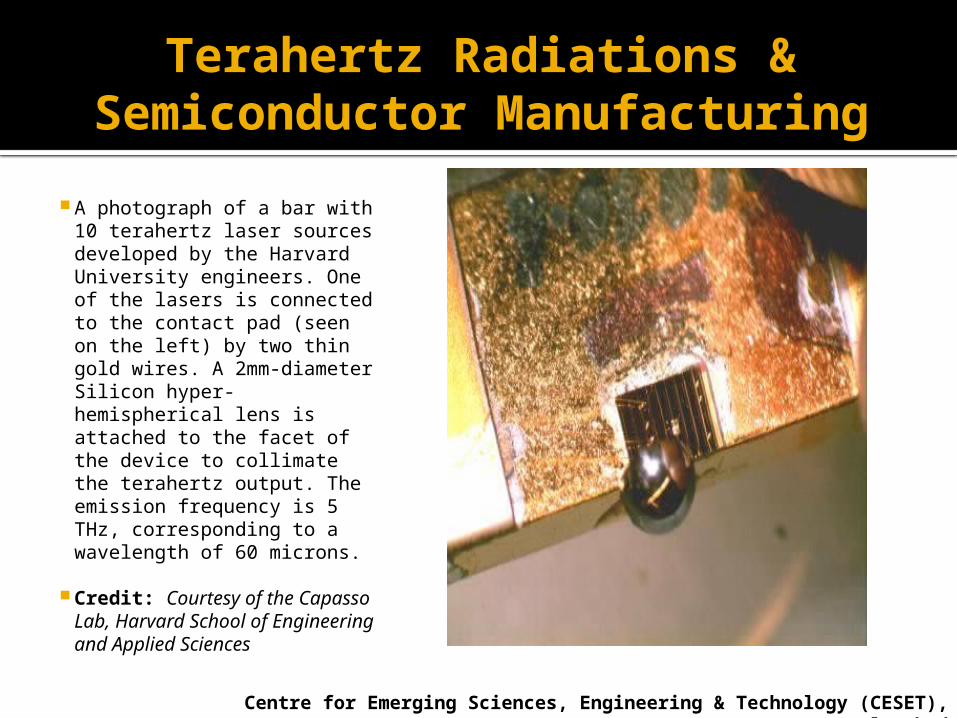
A photograph of a bar with 10 terahertz laser sources developed by the Harvard University engineers. One of the lasers is connected to the contact pad (seen on the left) by two thin gold wires. A 2mm-diameter Silicon hyper-hemispherical lens is attached to the facet of the device to collimate the terahertz output. The emission frequency is 5 THz, corresponding to a wavelength of 60 microns.
Credit: Courtesy of the Capasso Lab, Harvard School of Engineering and Applied Sciences
Centre for Emerging Sciences, Engineering & Technology (CESET), Islamabad
Terahertz Radiations & Semiconductor Manufacturing
Terahertz Radiations & Semiconductor Manufacturing
Centre for Emerging Sciences, Engineering & Technology (CESET), Islamabad
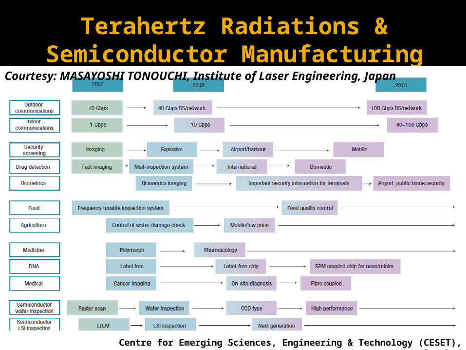
Courtesy: MASAYOSHI TONOUCHI, Institute of Laser Engineering, Japan
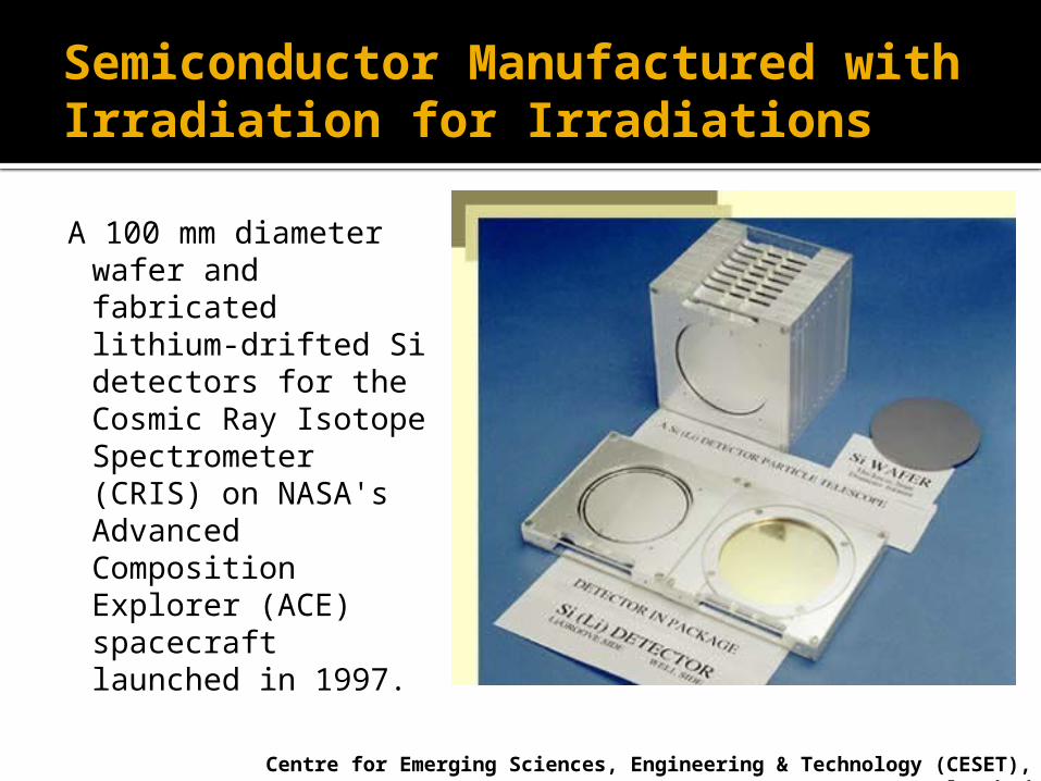
Semiconductor Manufactured with Irradiation for Irradiations
A 100 mm diameter wafer and fabricated lithium-drifted Si detectors for the Cosmic Ray Isotope Spectrometer (CRIS) on NASA's Advanced Composition Explorer (ACE) spacecraft launched in 1997.
Centre for Emerging Sciences, Engineering & Technology (CESET), Islamabad

A 20 by 20 orthogonal-strip lithium-drifted Si detector for imaging and high-resolution spectroscopy measurements. The active part of the detector is 46 mm by 46 mm by 3.5 mm thick. These detectors may be operated at relatively high temperatures (above 200K) while still maintaining low noise performance.
Centre for Emerging Sciences, Engineering & Technology (CESET), Islamabad
Semiconductor Manufactured with Irradiation for Irradiations
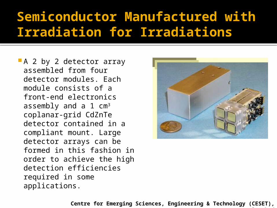
A 2 by 2 detector array assembled from four detector modules. Each module consists of a front-end electronics assembly and a 1 cm3 coplanar-grid CdZnTe detector contained in a compliant mount. Large detector arrays can be formed in this fashion in order to achieve the high detection efficiencies required in some applications.
Centre for Emerging Sciences, Engineering & Technology (CESET), Islamabad
Semiconductor Manufactured with Irradiation for Irradiations
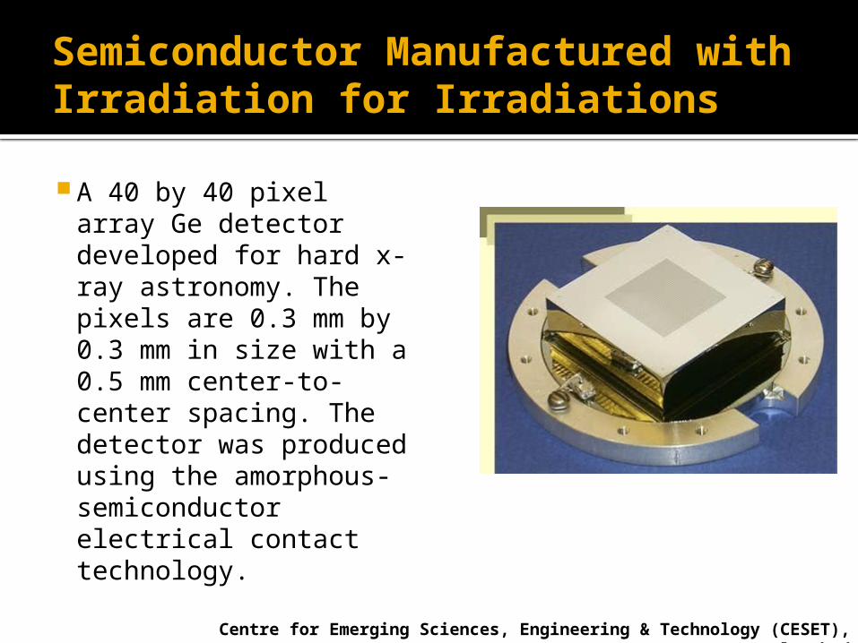
A 40 by 40 pixel array Ge detector developed for hard x-ray astronomy. The pixels are 0.3 mm by 0.3 mm in size with a 0.5 mm center-to-center spacing. The detector was produced using the amorphous-semiconductor electrical contact technology.
Centre for Emerging Sciences, Engineering & Technology (CESET), Islamabad
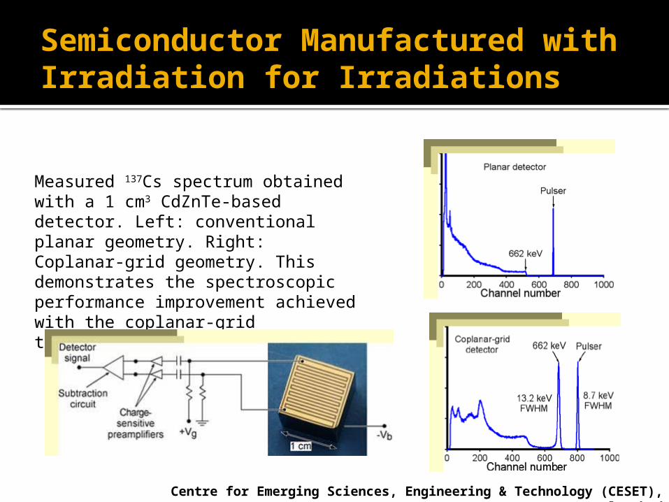
Semiconductor Manufactured with Irradiation for Irradiations
Centre for Emerging Sciences, Engineering & Technology (CESET), Islamabad
Measured 137Cs spectrum obtained with a 1 cm3 CdZnTe-based detector. Left: conventional planar geometry. Right: Coplanar-grid geometry. This demonstrates the spectroscopic performance improvement achieved with the coplanar-grid technique.
Semiconductor Manufactured with Irradiation for Irradiations
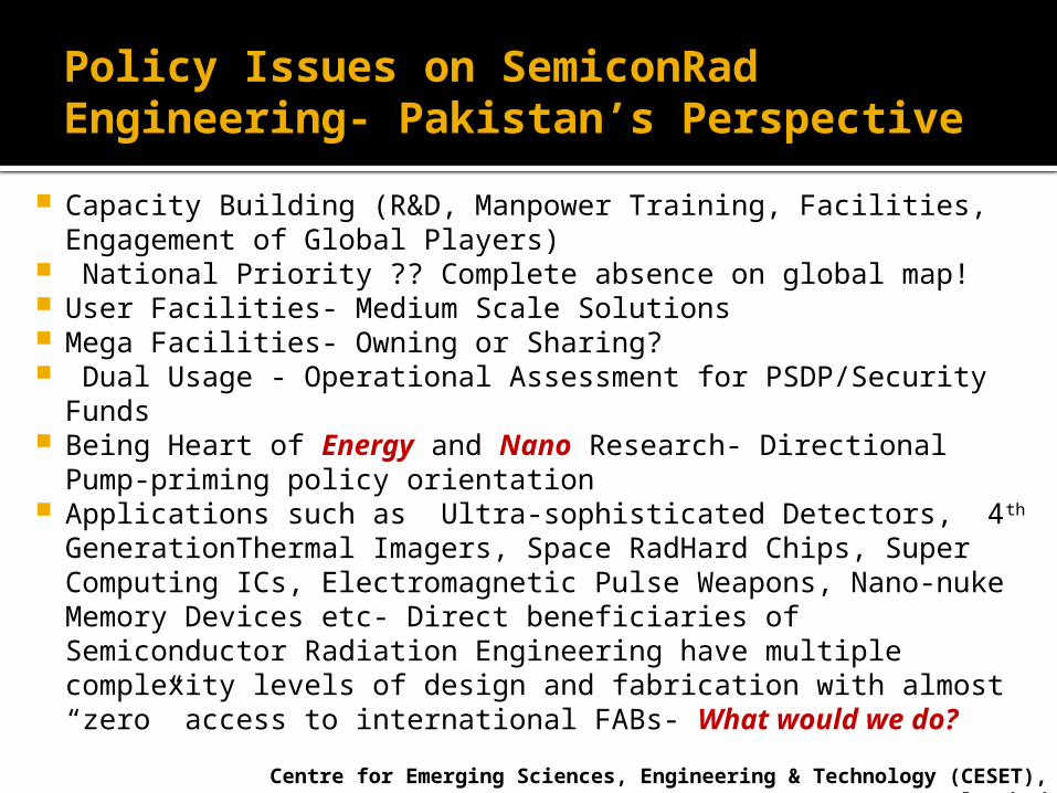
Policy Issues on SemiconRad Engineering- Pakistan’s Perspective
Centre for Emerging Sciences, Engineering & Technology (CESET), Islamabad
Capacity Building (R&D, Manpower Training, Facilities, Engagement of Global Players)
National Priority ?? Complete absence on global map! User Facilities- Medium Scale Solutions Mega Facilities- Owning or Sharing? Dual Usage - Operational Assessment for PSDP/Security Funds Being Heart of Energy and Nano Research- Directional Pump-
priming policy orientation Applications such as Ultra-sophisticated Detectors, 4th
GenerationThermal Imagers, Space RadHard Chips, Super Computing ICs, Electromagnetic Pulse Weapons, Nano-nuke Memory Devices etc- Direct beneficiaries of Semiconductor Radiation Engineering have multiple complexity levels of design and fabrication with almost “zero” access to international FABs- What would we do?
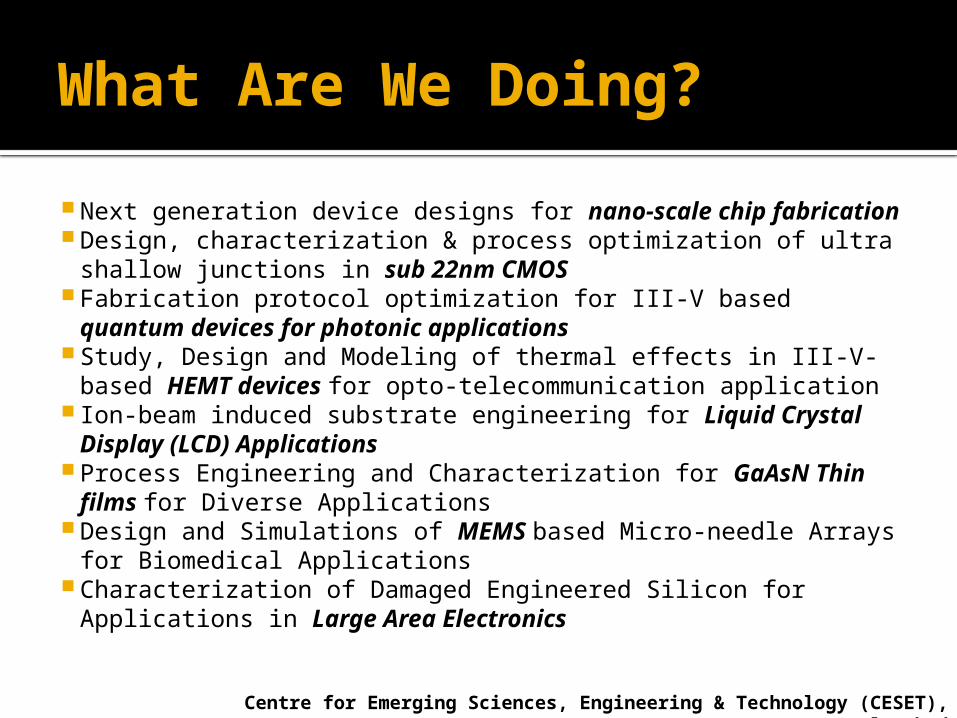
What Are We Doing?
Centre for Emerging Sciences, Engineering & Technology (CESET), Islamabad
Next generation device designs for nano-scale chip fabrication
Design, characterization & process optimization of ultra shallow junctions in sub 22nm CMOS
Fabrication protocol optimization for III-V based quantum devices for photonic applications
Study, Design and Modeling of thermal effects in III-V-based HEMT devices for opto-telecommunication application
Ion-beam induced substrate engineering for Liquid Crystal Display (LCD) Applications
Process Engineering and Characterization for GaAsN Thin films for Diverse Applications
Design and Simulations of MEMS based Micro-needle Arrays for Biomedical Applications
Characterization of Damaged Engineered Silicon for Applications in Large Area Electronics
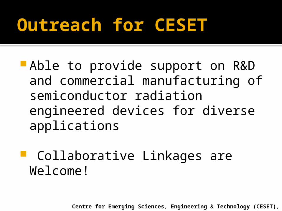
Outreach for CESET
Centre for Emerging Sciences, Engineering & Technology (CESET), Islamabad
Able to provide support on R&D and commercial manufacturing of semiconductor radiation engineered devices for diverse applications
Collaborative Linkages are Welcome!
Related Documents