Power Benefit Study for Ultra-High Density Transistor-Level Monolithic 3D ICs Young-Joon Lee, Daniel Limbrick, and Sung Kyu Lim School of ECE, Georgia Institute of Technology, Atlanta, GA [email protected], [email protected], [email protected] ABSTRACT The nano-scale 3D interconnects available in monolithic 3D IC technology enable ultra-high density device integration at the indi- vidual transistor-level. In this paper we demonstrate the power ben- efits of transistor-level monolithic 3D designs. We first build a cell library that consists of 3D gates and model their timing/power char- acteristics. Next, we build timing-closed, full-chip GDSII layouts and perform sign-off iso-performance power comparisons with 2D IC designs. We also study the characteristics of benchmark circuits that maximize the power benefits in monolithic 3D designs. Lastly, our study is extended to predict the power benefits of monolithic 3D designs built with future devices. Categories and Subject Descriptors B.8.2 [Performance and Reliability]: Performance Analysis and Design Aids General Terms Design Keywords 3D IC, monolithic 3D, transistor-level, power analysis 1. INTRODUCTION To better exploit the benefits from 3D die stacking, monolithic 3D technology is currently being investigated as a next generation technology. In a monolithic 3D IC, the device layers are fabri- cated sequentially. When the top layer is attached to the bottom layer, the top layer is a blank silicon. Alignment precision is de- termined by lithography stepper accuracy, which is around 10nm today. Also, the top layer can be made very thin, around 30nm [1]. Thus, monolithic inter-tier vias (MIVs) for vertical connections are very small—about two orders of magnitude smaller than through- silicon-via (TSV)—with almost negligible parasitic RC. With these small MIVs, designers can truly exploit the benefit of vertical di- mension. The early works for monolithic 3D ICs were technology-driven [6, 4, 9]. Recently, logic design methodologies for monolithic 3D ICs were demonstrated [2, 8, 7]. In these works, the authors pre- sented various comparisons among monolithic 3D ICs and TSV- Permission to make digital or hard copies of all or part of this work for personal or classroom use is granted without fee provided that copies are not made or distributed for profit or commercial advantage and that copies bear this notice and the full citation on the first page. To copy otherwise, to republish, to post on servers or to redistribute to lists, requires prior specific permission and/or a fee. DAC’13, May 29 - June 07 2013, Austin, TX, USA. Copyright 2013 ACM 978-1-4503-2071-9/13/05 ...$15.00. based 3D ICs and conventional 2D ICs in terms of footprint, tim- ing, and power. However, timing was not closed in these works, which make the studies not practical. In addition, all these works assume that the timing and power characteristics of 3D monolithic gates are the same as 2D gates and did not demonstrate why that is a reasonable assumption. The authors also did not provide in- depth analyses and discussions on why monolithic 3D technology reduces power consumption and what factors affect the power re- duction margin. This knowledge is crucial to maximize the benefit and justify on-going and future research on fabrication and design technologies for monolithic 3D ICs. As discussed in [2, 8], monolithic 3D technology enables a very fine-grained 3D circuit partitioning. We can divide standard cells into PMOS and NMOS parts, place them in different layers, and connect them using MIVs, which we call transistor-level mono- lithic 3D integration (T-MI) in this paper. Or, as in TSV-based 3D ICs, we may place planar cells in different layers and connect them using MIVs, which is named gate-level monolithic 3D integration (G-MI). In this paper we focus on transistor-level integration that allows the highest integration density possible. The T-MI designs are different from G-MI: (1) Most of the 3D interconnects are em- bedded in the cells. (2) PMOS and NMOS transistors are on dif- ferent layers, thus manufacturing processes can be optimized sepa- rately. (3) Physical layout (placement, routing, optimization, etc.) can be performed using existing 2D electronic design automation (EDA) tools, with modifications. In this paper, we study the power benefit of T-MI based on timing- closed, detailed routing completed GDSII-level layouts and sign- off analysis on timing and power. Our comprehensive work en- compasses device and interconnect-level study, gate-level modeling and optimization, and full-chip layout constructions, optimization, and timing/power analysis for the current and future technology nodes. With our layout-based simulations and in-depth analyses, we demonstrate how to maximize the power benefit of T-MI tech- nology. For fair comparisons between 3D and 2D designs, timing is closed on all designs (iso-performance), and power consumption is compared. We also investigate the circuit characteristics that affect the power benefit of monolithic 3D ICs. Our major contributions are as follows: (1) To the best of our knowledge, this is the first work to characterize the timing and power of the individual transistor-level monolithic 3D cells. We extract the internal parasitic RC of our T-MI cells and character- ize their timing and power. We then compare T-MI cells with 2D counterparts. (2) We study the design aspects that significantly af- fect the power benefit of monolithic 3D ICs. We discuss what kind of logic circuits are suitable for power reduction in monolithic 3D ICs. In addition, we demonstrate that the power reduction rate also depends on the target clock period. (3) We build the libraries and full-chip layouts for monolithic 3D ICs implemented using 7nm de- vices. The goal is to predict the future trend of power saving with

Welcome message from author
This document is posted to help you gain knowledge. Please leave a comment to let me know what you think about it! Share it to your friends and learn new things together.
Transcript

Power Benefit Study for Ultra-High DensityTransistor-Level Monolithic 3D ICs
Young-Joon Lee, Daniel Limbrick, and Sung Kyu LimSchool of ECE, Georgia Institute of Technology, Atlanta, GA
[email protected], [email protected], [email protected]
ABSTRACTThe nano-scale 3D interconnects available in monolithic 3D ICtechnology enable ultra-high density device integration at the indi-vidual transistor-level. In this paper we demonstrate the power ben-efits of transistor-level monolithic 3D designs. We first build a celllibrary that consists of 3D gates and model their timing/power char-acteristics. Next, we build timing-closed, full-chip GDSII layoutsand perform sign-off iso-performance power comparisons with 2DIC designs. We also study the characteristics of benchmark circuitsthat maximize the power benefits in monolithic 3D designs. Lastly,our study is extended to predict the power benefits of monolithic3D designs built with future devices.
Categories and Subject DescriptorsB.8.2 [Performance and Reliability]: Performance Analysis andDesign Aids
General TermsDesign
Keywords3D IC, monolithic 3D, transistor-level, power analysis
1. INTRODUCTIONTo better exploit the benefits from 3D die stacking, monolithic
3D technology is currently being investigated as a next generationtechnology. In a monolithic 3D IC, the device layers are fabri-cated sequentially. When the top layer is attached to the bottomlayer, the top layer is a blank silicon. Alignment precision is de-termined by lithography stepper accuracy, which is around 10nmtoday. Also, the top layer can be made very thin, around 30nm [1].Thus, monolithic inter-tier vias (MIVs) for vertical connections arevery small—about two orders of magnitude smaller than through-silicon-via (TSV)—with almost negligible parasitic RC. With thesesmall MIVs, designers can truly exploit the benefit of vertical di-mension.
The early works for monolithic 3D ICs were technology-driven[6, 4, 9]. Recently, logic design methodologies for monolithic 3DICs were demonstrated [2, 8, 7]. In these works, the authors pre-sented various comparisons among monolithic 3D ICs and TSV-
Permission to make digital or hard copies of all or part of this work forpersonal or classroom use is granted without fee provided that copies arenot made or distributed for profit or commercial advantage and that copiesbear this notice and the full citation on the first page. To copy otherwise, torepublish, to post on servers or to redistribute to lists, requires prior specificpermission and/or a fee.DAC’13, May 29 - June 07 2013, Austin, TX, USA.Copyright 2013 ACM 978-1-4503-2071-9/13/05 ...$15.00.
based 3D ICs and conventional 2D ICs in terms of footprint, tim-ing, and power. However, timing was not closed in these works,which make the studies not practical. In addition, all these worksassume that the timing and power characteristics of 3D monolithicgates are the same as 2D gates and did not demonstrate why thatis a reasonable assumption. The authors also did not provide in-depth analyses and discussions on why monolithic 3D technologyreduces power consumption and what factors affect the power re-duction margin. This knowledge is crucial to maximize the benefitand justify on-going and future research on fabrication and designtechnologies for monolithic 3D ICs.
As discussed in [2, 8], monolithic 3D technology enables a veryfine-grained 3D circuit partitioning. We can divide standard cellsinto PMOS and NMOS parts, place them in different layers, andconnect them using MIVs, which we call transistor-level mono-lithic 3D integration (T-MI) in this paper. Or, as in TSV-based 3DICs, we may place planar cells in different layers and connect themusing MIVs, which is named gate-level monolithic 3D integration(G-MI). In this paper we focus on transistor-level integration thatallows the highest integration density possible. The T-MI designsare different from G-MI: (1) Most of the 3D interconnects are em-bedded in the cells. (2) PMOS and NMOS transistors are on dif-ferent layers, thus manufacturing processes can be optimized sepa-rately. (3) Physical layout (placement, routing, optimization, etc.)can be performed using existing 2D electronic design automation(EDA) tools, with modifications.
In this paper, we study the power benefit of T-MI based on timing-closed, detailed routing completed GDSII-level layouts and sign-off analysis on timing and power. Our comprehensive work en-compasses device and interconnect-level study, gate-level modelingand optimization, and full-chip layout constructions, optimization,and timing/power analysis for the current and future technologynodes. With our layout-based simulations and in-depth analyses,we demonstrate how to maximize the power benefit of T-MI tech-nology. For fair comparisons between 3D and 2D designs, timing isclosed on all designs (iso-performance), and power consumption iscompared. We also investigate the circuit characteristics that affectthe power benefit of monolithic 3D ICs.
Our major contributions are as follows: (1) To the best of ourknowledge, this is the first work to characterize the timing andpower of the individual transistor-level monolithic 3D cells. Weextract the internal parasitic RC of our T-MI cells and character-ize their timing and power. We then compare T-MI cells with 2Dcounterparts. (2) We study the design aspects that significantly af-fect the power benefit of monolithic 3D ICs. We discuss what kindof logic circuits are suitable for power reduction in monolithic 3DICs. In addition, we demonstrate that the power reduction rate alsodepends on the target clock period. (3) We build the libraries andfull-chip layouts for monolithic 3D ICs implemented using 7nm de-vices. The goal is to predict the future trend of power saving with
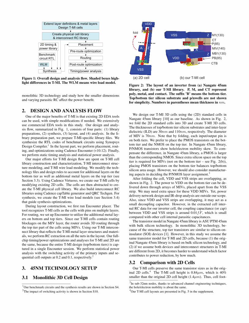
Extend layer definitions & metal layers
Design T-MI cells
Synthesis
Placement
Pre-route optimization
Routing
Post-route optimization
Timing/power analysis
WLM
Benchmark
circuit RTL
Create physical cell library
& interconnect RC library
2D timing &
power library
Figure 1: Overall design and analysis flow. Shaded boxes high-light differences in T-MI. The WLM means wire load model.
monolithic 3D technology and study how the smaller dimensionsand varying parasitic RC affect the power benefit.
2. DESIGN AND ANALYSIS FLOWOne of the major benefits of T-MI is that existing 2D EDA tools
can be used, with simple modifications if needed. We extensivelyuse commercial EDA tools in this study. Our design and analy-sis flow, summarized in Fig. 1, consists of four parts: (1) librarypreparations, (2) synthesis, (3) layout, and (4) analysis. In the li-brary preparation part, we prepare T-MI-specific library files. Wesynthesize the RTL codes of benchmark circuits using SynopsysDesign Compiler.1 In the layout part, we perform placement, rout-ing, and optimizations using Cadence Encounter (v10.12). Finally,we perform static timing analysis and statistical power analysis.
Our major efforts for T-MI design flow are spent on T-MI celllibrary construction and characterization, T-MI interconnect struc-ture modeling, and T-MI wire load modeling. We modify the tech-nology files and design rules to account for additional layers on thebottom tier as well as additional metal layers on the top tier (seeSection 3.3). Using Cadence Virtuoso, we create our T-MI cells bymodifying existing 2D cells. The cells are then abstracted to cre-ate the T-MI physical cell library. We also build interconnect RClibraries using Cadence capTable generator and QRC Techgen. Forsynthesis, we create the T-MI wire load models (see Section 3.4)that guide synthesis optimizations.
During layout construction, we first run Encounter placer. Thetool recognizes T-MI cells as the cells with pins on multiple layers.For routing, we set up Encounter to utilize the additional metal lay-ers on bottom and top tiers. Since our T-MI cells contain routingblockages on the MIV layer, the router avoids 3D routing throughthe top tier part of the cells using MIVs. Using our T-MI intercon-nect library that reflects the T-MI metal layer structures and materi-als, we perform RC extraction on all the nets in the layout. Our full-chip timing/power optimizations and analyses for T-MI and 2D arethe same, because the entire T-MI design (top/bottom tiers) is cap-tured in a single Encounter session. We perform statistical poweranalysis with the switching activity of the primary inputs and se-quential cell outputs at 0.2 and 0.1, respectively.2
3. 45NM TECHNOLOGY SETUP
3.1 Monolithic 3D Cell Design1Our benchmark circuits and the synthesis results are shown in Section S4.2The impact of switching activity is shown in Section S10.
(a) 2D cell
VSS
VSS
VDD
VDD
Z
Z MB1(130)
MIV(140)
CT
CTB
PB(85)
P(85)
M1(130)Z
AA
(b) our T-MI cell
fold
Figure 2: The layout of an inverter from (a) Nangate 45nmlibrary, and (b) our T-MI library. P, M, and CT representpoly, metal, and contact. The suffix ’B’ means the bottom tier.Top/bottom tier silicon substrate and p/nwells are not shownfor simplicity. Numbers in parentheses mean thickness in nm.
We design our T-MI 3D cells using the (2D) standard cells inNangate 45nm library [10] as our baseline. As shown in Fig. 2,we fold the 2D standard cells into 3D and create T-MI 3D cells.The thicknesses of top/bottom tier silicon substrates and inter-layerdielectric (ILD) are 30nm and 110nm, respectively. The diameterof MIV is 70nm. Note that by folding, each input/output pin ison both tiers. We prefer to place the PMOS transistors on the bot-tom tier and the NMOS on the top tier. In Nangate 45nm library,P/NMOS transistors show hole/electron mobility skew. To com-pensate the difference, in Nangate 45nm library, a PMOS is largerthan the corresponding NMOS. Since extra silicon space on the toptier is required for MIVs (not on the bottom tier – see Fig. 2(b)),placing PMOS transistors on the bottom tier balances top/bottomsilicon area usage. However, we should also consider manufactur-ing aspects in deciding the P/NMOS layer assignment.3
After folding the cell, VDD and VSS strips are overlapping, asshown in Fig. 2. The power to VDD on the bottom tier can be de-livered down through arrays of MIVs, placed apart from the VSSstrip. We may need extra space for these VDD MIVs. Yet, powerdelivery network design and IR-drop analysis are outside our scope.Also, since VDD and VSS strips are overlapping, it may act as asmall decoupling capacitor. However, in the extracted cell inter-nal RC data for our inverter cell, the coupling capacitance (or cap)between VDD and VSS strips is around 0.01fF , which is smallcompared with other cell internal parasitic capacitances.
The transistor model in Nangate 45nm library is ASU PTM 45nmwith bulk silicon technology. In monolithic 3D technology, be-cause of the structure, top tier transistors are similar to silicon-on-insulator (SOI) devices [1]. However, in this study we assume thesame transistor model for T-MI and 2D cells, because (1) the orig-inal Nangate 45nm library is based on bulk silicon technology, and(2) if we assume both devices and interconnect structures in T-MIare different from 2D, it becomes harder to understand which factorcontributes to power reduction, by how much.
3.2 Comparison with 2D CellsOur T-MI cells preserve the same transistor sizes as in the orig-
inal 2D cells.4 The T-MI cell height is 0.84µm, which is 40%smaller than the original 2D cell height (1.4µm). Thus, cell foot-3In sub-32nm nodes, thanks to advanced channel engineering techniques,the hole/electron mobility is about the same.4Our T-MI cell layouts are presented in Fig. 5 in the supplement.

Table 1: Cell internal parasitic RC values. The 3D-c means 3Dwith top tier silicon modeled as a conductor.
R (kΩ) C (fF )cell 2D 3D 3D-c 2D 3D 3D-cINV 0.186 0.107 0.107 0.363 0.368 0.349
NAND2 0.372 0.237 0.237 0.561 0.586 0.547MUX2 1.133 0.975 0.975 1.823 1.938 1.796
DFF 2.876 3.045 3.045 4.108 5.101 4.740
print reduces by 40%. The reasons why it is not 50% are (1)P/NMOS size mismatch incurs extra space on NMOS side, and (2)MIVs require extra space on the top tier.
When designing T-MI cells, care should be taken to reduce cellinternal parasitic RC. As shown in Fig. 2(b), the connection fromthe PMOS on the bottom tier to the NMOS on the top tier needs togo through CTB, MB1, MIV, CT, M1, then CT to diffusion. This3D path may become larger than the original 2D path and may in-crease cell internal parasitic RC. Similarly, the path from the PB onthe bottom tier to the P on the top tier goes through multiple layers.To reduce cell internal parasitic RC, it is important to minimize thelengths of 3D paths. To achieve shorter 3D paths, we should placeMIVs close to the connecting transistors. We also need to utilizedirect source/drain (S/D) contacts (see Fig. 5(c) in the supplement).The direct S/D contacts reduce the detour in the 3D paths and un-necessary parasitic RC.
We examine the cell internal parasitic RC of 3D and 2D cellsand the impact on timing/power. In previous works [2, 8, 7], theauthors assumed that the delay and power of 3D cells are the sameas 2D cells and used 2D timing/power library. In [1], the authorsfabricated a transistor-level monolithic 3D IC and measured thetop/bottom transistor performances. They reported that the differ-ences between 3D transistors and baseline 2D transistors were neg-ligible. Yet, the delay and power of cells are also affected by cellinternal parasitic RC. From Fig. 2(b), we can conjecture that thereare coupling capacitances among PB, CTB, MB1, MIV, CT, andM1. Using Mentor Graphics Calibre XRC with EM-simulation-based extraction rules, we extract these capacitance values as wellas resistances and transistors from our T-MI cell layout. Then, wegenerate a SPICE netlist of the cell that consists of transistors andparasitic RC components.
Since Calibre XRC is designed for 2D ICs, it can only model onediffusion layer. Due to this tool limitation, top tier diffusion layercan be modeled as either dielectric or conductor. Even though thetop tier silicon is doped (low resistivity) and the bodies of top tiertrasistors are tied to the ground, we expect that some amount ofelectric field may penetrate the top tier silicon and coupling amongtop and bottom tier objects (M1, MB1, P, PB, etc.) may exist. Whenwe assume that the top tier silicon is dielectric, the coupling be-tween top and bottom tier objects would be overestimated; when itis conductor, the coupling would be underestimated. The real casewould be between these two extreme cases.
The total cell internal RC values, extracted from the original 2Dcells and our 3D (T-MI) cells, are shown in Table 1. For 3D case,the results with top tier silicon as both dielectric (3D) and conductor(3D-c) are shown. From the results, we observe the followings: (1)For INV, NAND2, and MUX2, the R values of 3D are noticeablysmaller than 2D counterparts, because we reduce the length of polyand metal lines inside the cells, using 3D interconnects. (2) TheC values of 3D are comparable with those of 2D – the 2D value isbetween 3D and 3D-c. (3) For DFF, both R and C of 3D are largerthan 2D counterparts. Due to the complex internal connections, wecould not create a 3D cell layout that match parasitic RC of 2D. Insummary, depending on the cell layout complexity, the internal RC
Table 2: Delay and internal power consumption of cells withvarious input slew and load capacitance conditions. The li-brary uses different input slew settings for DFF. The values inthe parentheses mean the percentage ratio of 3D to 2D.
delay (ps) power (fJ)cell 2D 3D 2D 3D
fast case: input slew=7.5ps (5ps for DFF), load cap.=0.8fFINV 17.2 16.9 (98.3%) 0.383 0.351 (91.6%)
NAND2 21.2 20.9 (98.6%) 0.616 0.583 (94.6%)MUX2 59.8 58.2 (97.3%) 2.113 2.060 (97.5%)DFF 108.8 113.4 (104.2%) 6.341 6.735 (106.2%)
medium case: input slew=37.5ps (28.1ps for DFF), load cap.=3.2fFINV 51.1 50.8 (99.4%) 0.362 0.343 (94.8%)
NAND2 56.2 55.9 (99.5%) 0.604 0.581 (96.2%)MUX2 97.0 95.3 (98.2%) 2.239 2.168 (96.8%)DFF 142.6 147.0 (103.1%) 6.358 6.756 (106.3%)
slow case: input slew=150ps (112.5ps for DFF), load cap.=12.8fFINV 188.3 188.0 (99.8%) 0.449 0.431 (96.0%)
NAND2 195.9 195.5 (99.8%) 0.698 0.675 (96.7%)MUX2 215.1 212.5 (98.8%) 2.555 2.487 (97.3%)DFF 237.4 243.3 (102.5%) 7.303 7.659 (104.9%)
Table 3: Summary of metal layers. Unit is nm.level metal layers width spacing thickness
global 2D:M7-8, 3D:M10-11 400 400 800intermediate 2D:M4-6, 3D:M7-9 140 140 280
local 2D:M2-3, 3D:M2-6 70 70 140M1 2D:M1, 3D:MB1,M1 70 65 130
ratio between 3D and 2D may vary.Yet, the delay and power of the cells are more important met-
rics. We perform cell timing/power characterizations using com-mercial softwares. The SPICE netlists obtained from the previousRC extractions are fed into Cadence Encounter Library Character-izer, which runs SPICE simulations to characterize delay and powerof cells under various input slew and load capacitance conditions.The delay/power of 3D and 2D cells are shown in Table 2. The val-ues are obtained from the data tables in the characterized Liberty li-brary. The delay is the cell internal delay including load effect, andthe power is the dynamic power consumed within cell boundary(including short circuit power and power for gate/parasitic capaci-tances). We observe that for INV, NAND2, and MUX2, the delayand power of 3D are slightly better than 2D, whereas for DFF, theyare a little worse. In addition, as the input slew and load capacitancecondition changes from fast to slow case, the difference between T-MI and 2D becomes smaller. Note that depending on cell designquality and manufacturing technology, the results may change. Webelieve that with proper cell designs, the delay and power of 3Dcells could be similar to 2D counterparts.
3.3 Monolithic Interconnect SetupOur T-MI interconnect structure is an extension of the Nangate
(2D) 45nm library. As shown in Table 3, we use 8 out of 10 metallayers in the Nangate 45nm. For T-MI, we make two modifications:We add (1) a new metal layer on the bottom tier (MB1), and (2)three local metal layers on the top tier (M4-6).5
With T-MI cell folding, the cells become 40% smaller than 2D(see Section 3.2). This results in about 40-50% smaller core foot-print area. As a result, the cell pin density in T-MI becomes about1.7-2X larger than in 2D, leading to a higher routing demand perunit area (or routing tile). To satisfy the high routing demand, weneed to increase the routing capacity (#routing tracks per routingtile). The most area-efficient way is to add local metal layers, be-5Our 2D and T-MI metal layers are shown in Fig. 9 in the supplement.
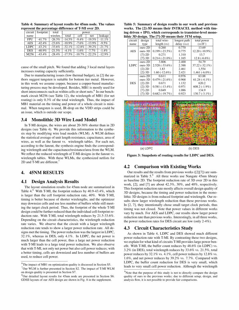
Table 4: Summary of layout results for 45nm node. The valuesrepresent the percentage difference of T-MI over 2D.
circuit footprint total powername wirelen. total cell net leakageFPU -41.7% -26.3% -14.5% -9.4% -19.5% -11.1%AES -42.4% -23.6% -10.9% -7.6% -13.9% -9.5%
LDPC -43.2% -33.6% -32.1% -12.8% -39.2% -21.7%DES -40.9% -21.5% -4.1% -1.6% -7.7% -1.4%M256 -43.4% -28.4% -17.5% -10.7% -22.2% -12.9%
cause of the small pitch. We found that adding 3 local metal layersincreases routing capacity sufficiently.
Due to manufacturing issues (low thermal budget), in [2] the au-thors suggest tungsten is suitable for bottom tier metal. However,in this work we assume copper, because a copper-based manufac-turing process may be developed. Besides, MB1 is mostly used forshort interconnects such as within cells or short nets.6 In our bench-mark circuit M256 (see Table 12), the wirelength of MB1 (for netrouting) is only 0.3% of the total wirelength. Thus, the impact ofMB1 material on the timing and power of a whole circuit is mini-mal. When tungsten is used, IR-drop on the VDD strips could bean issue, which is outside our scope.
3.4 Monolithic 3D Wire Load ModelIn T-MI designs, the wires are about 20-30% shorter than in 2D
designs (see Table 4). We provide this information to the synthe-sis step by modifying wire load models (WLM). A WLM definesthe statistical average of unit length resistance, capacitance, area ofwires, as well as the fanout vs. wirelength tables. For each net,according to the fanout, the synthesis engine finds the correspond-ing wirelength and the capacitance/resistance/area from the WLM.We reflect the reduced wirelength of T-MI designs in the fanout vs.wirelength tables. With these WLMs, the synthesized netlists for2D and T-MI are different.7
4. 45NM RESULTS
4.1 Design Analysis ResultsThe layout simulation results for 45nm node are summarized in
Table 4.8 With T-MI, the footprint reduces by 40.9-43.4%, whichis larger than the cell footprint reduction rate, 40%. With T-MI,timing is better because of shorter wirelengths, and the optimizermay downsize cells and use less number of buffers while still meet-ing the target clock period. Thus, the footprint of the whole T-MIdesign could be further reduced than the individual cell footprint re-duction rate. With T-MI, total wirelength reduces by 21.5-33.6%.Depending on the circuit characteristics, the wirelength reductionrate varies. We observe that the circuit with a larger wirelengthreduction rate tends to show a larger power reduction rate. All de-signs met the timing. The power reduction was the largest in LDPC,32.1%, whereas in DES, only 4.1%. In LDPC, the net power ismuch larger than the cell power, thus a large net power reductionwith T-MI leads to a large total power reduction. We also observethat with T-MI, not only net power but also cell power reduces; witha better timing, cells are downsized and less number of buffers areused, to reduce cell power.
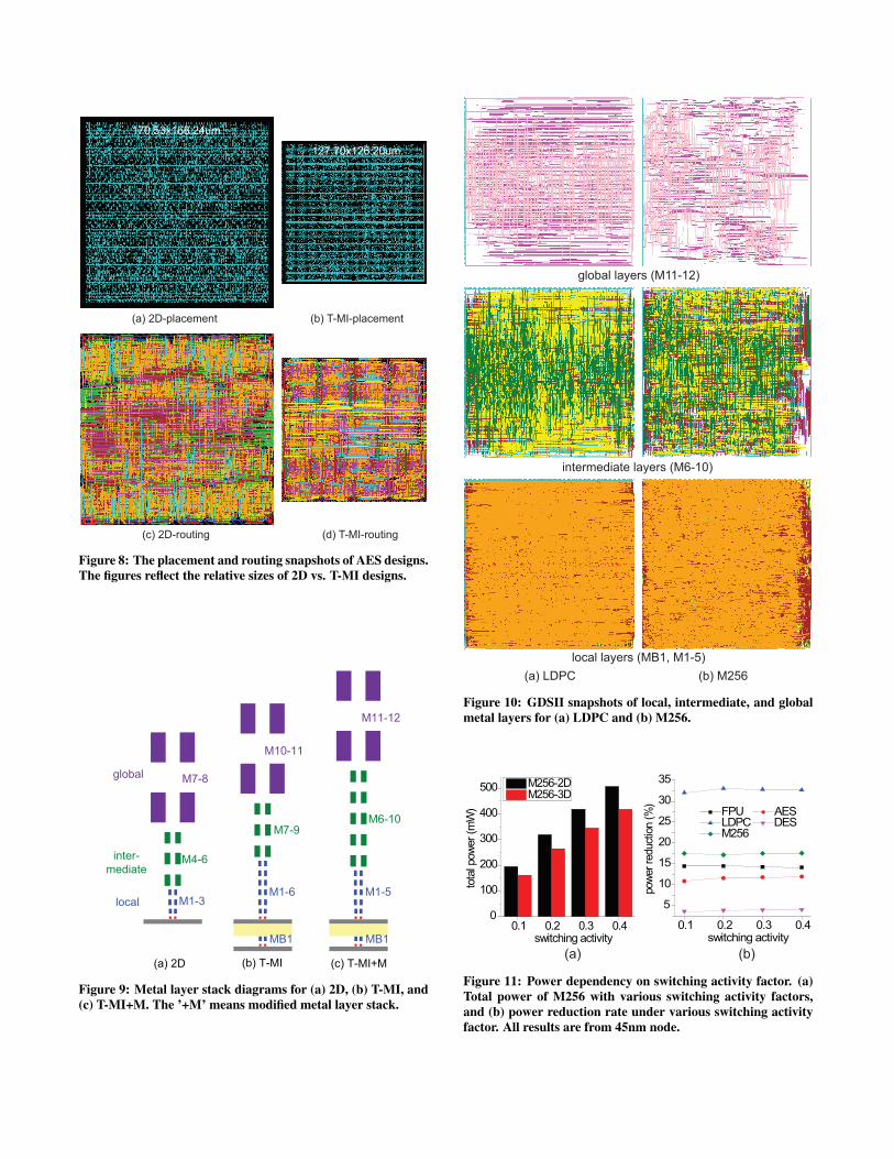
6The impact of MB1 on optimization quality is discussed in Section S5.7Our WLM is further presented in Section S2. The impact of T-MI WLMon design quality is presented in Section S7.8Our detailed layout results for 45nm node are presented in Section S6.GDSII layouts of our AES design are shown in Fig. 8 in the supplement.
Table 5: Summary of design results in our work and previousworks. The [2]-3D means their INTRACEL method with tim-ing driven + IPO, which corresponds to transistor-level mono-lithic 3D design. The [7]-3D means their 3TM setup.
circuit design total wire- longest path total powername type length (m) delay (ns) (mW )
ours-2D 0.260 0.770 13.69AES ours-3D 0.199 (-23.5%) 0.775 12.20 (-10.9%)
[7]-2D 0.271 1.310 13.7[7]-3D 0.214 (-21.0%) 1.165 12.8 (-6.6%)
ours-2D 3.806 2.400 54.79LDPC ours-3D 2.528 (-33.6%) 2.388 37.22 (-32.1%)
[2]-2D 1.83 2.461 1,554[2]-3D 1.60 (-12.6%) 2.421 1,461 (-6.0%)
ours-2D 0.611 0.976 63.88ours-3D 0.479 (-21.6%) 0.968 61.24 (-4.1%)
DES [2]-2D 0.671 1.132 620.2[2]-3D 0.581 (-13.4%) 0.971 608.2 (-1.9%)[7]-2D 0.849 1.086 134.9[7]-3D 0.682 (-19.7%) 0.923 130.7 (-3.1%)
(a) LDPC
footprint = 457.83x456.4um
wirelength = 3.806m
footprint = 331.88x330.4um
wirelength=0.611m
(b) DES
Figure 3: Snapshots of routing results for LDPC and DES.
4.2 Comparison with Existing WorksOur results and the results from previous works ([2][7]) are sum-
marized in Table 5.9 All three works use Nangate 45nm libraryas baseline 2D. The footprint reduction rate of 3D over 2D in thiswork, [2], and [7] are about 42.3%, 30%, and 40%, respectively.This footprint reduction rate mostly affects overall design quality of3D designs, because the timing and power reduction in the mono-lithic 3D designs is from reduced footprint and wirelength. Our re-sults show larger wirelength reduction than these previous works.In [2, 7], they intentionally chose small target clock periods, thustiming was not closed. Note that power values in different worksvary by much. For AES and LDPC, our results show larger powerreduction rate than previous works. Interestingly, in all three works,the power reduction rates for DES circuit are low (only 2-4%).
4.3 Circuit Characteristics StudyAs shown in Table 4, LDPC and DES showed much different
power reduction rate with T-MI. By contrasting these two designs,we explain for what kind of circuits T-MI provides large power ben-efit. With T-MI, the buffer count reduces by 48.6% (in LDPC) vs.3.2% (in DES), total wirelength reduces by 33.6% vs. 21.5%, totalpower reduces by 32.1% vs. 4.1%, cell power reduces by 12.8% vs.1.6%, and net power reduces by 39.2% vs. 7.7%. Compared withLDPC, the buffer count reduction for DES is very small, whichleads to very small cell power reduction. Although the wirelength9Note that the purpose of this study is not to directly compare the designquality of ours to the previous works; due to different setup, design, andanalysis flow, it is not possible to provide fair comparisons.

(a) AES (b) M256(1.0ns) (0.8ns) (0.72ns) (2.6ns) (2.4ns) (2.0ns)
slow medium fast
4
8
12
16
20
24
28re
duct
ion (%
) total power cell power net power leakage
slow medium fast
4
8
12
16
20
24
28
reduct
ion (%
)
Figure 4: Power reduction rate (T-MI over 2D) under varioustarget clock periods.
reduction in DES is not so small, the net power reduction rate is sig-nificantly smaller than LDPC. The net capacitance/power consistsof wire and (cell input) pin parts.10 For most nets in DES, wiresare very short. This difference is also observed in Fig. 3. In DESlayout, there are many small regions where cells are tightly con-nected inside but not so much to outside. For these short nets, pincapacitances dominate wire capacitances, thus reducing wirelengthdoes not reduce net power as much. Although these two circuitsare similar in size (#cells, nets) and average fanout, because of theinherent difference in circuit characteristics, the power benefit ofT-MI differs by much.
4.4 Impact of Target Clock PeriodThe power benefit of T-MI also depends on the target clock pe-
riod. For AES and M256, we vary the target clock period andperform full designs, from synthesis to layout optimizations. Thepower reduction rate is shown in Fig. 4. The trend is clear; whenthe target clock is faster, the power benefit of T-MI becomes larger.This is because at faster clock speeds, the timing of the 2D de-sign becomes harder to meet than T-MI, because of longer wires.The optimization engine uses more buffers and larger cells, lead-ing to steep increase in cell power. Thus, the cell power reductionrate increases noticeably as clock becomes faster. With faster clockspeeds, core footprint and wirelengths also become larger, leadingto larger net power reduction rate with T-MI.
5. 7NM TECHNOLOGY SETUPAnother major aspect that affects the power benefit of T-MI is the
technology node. As the technology advances, devices and wiresshrink at different speed, affecting timing/power of the circuit andchanging power benefit of T-MI. According to the latest ITRS 2011roadmap [5], 7nm node is near the end of the roadmap.11 In ITRSprojection for 7nm node, devices become dramatically efficient,however wires do not. The copper effective resistivity in 7nm is3.7X larger than in 45nm, due to size effects (edge scattering, etc.).
We now predict how the power benefit of T-MI changes in the fu-ture 7nm node. The comparison between our 45nm and 7nm setupis shown in Table 6. Since there is no real 7nm node data avail-able today, we scale down our 45nm library data as well as use datafrom ITRS projection. As a transistor model, we use ASU PTM-MG HP 7nm model [11]. The interconnect dimensions are scaleddown to (7/45)X = 0.156X, and the interconnect RC libraries are
10We provide wire vs. pin power breakdown in Section S8.11A summary of 45nm and 7nm node device and interconnect characteristicsfrom ITRS projections are shown in Table 10 in the supplement.
Table 6: Comparison of our 45nm and 7nm node setup.45nm 7nm
transistor planar multi-gateVDD (V ) 1.1 0.7
transistor length (drawn, nm) 50 11transistor width varies fixed
back-end-of-line ILD k 2.5 2.2M2 width (nm) 70 10.8
MIV diameter (nm) 70 10.8ILD thickness (nm) 110 50
standard cell height (um) 1.4 0.218
Table 7: Summary of layout results for 7nm node.circuit footprint total powername wirelen. total cell net leakageFPU -47.0% -34.2% -37.3% -32.4% -44.4% -21.0%AES -62.0% -47.8% -19.8% -10.3% -28.4% -28.5%
LDPC -42.9% -27.7% -19.1% -3.7% -26.6% -3.5%DES -40.8% -21.9% -3.4% -1.3% -7.3% -3.0%M256 -44.6% -23.0% -17.8% -14.1% -23.0% -2.4%
rebuilt, with a lower dielectric k (=2.2). We scale down the phys-ical shapes of cells to 0.156X. Based on preliminary SPICE simu-lations12, we also scale down cell input capacitance to 0.179X, celldelay to 0.471X, output slew to 0.420X, cell power to 0.084X, andcell leakage power to 0.678X. We apply these scaling factors tothe 45nm Liberty library and create our 7nm Liberty library. Sincethe transistors in 7nm node are not planar but multi-gate (e.g. Fin-FET), the coupling between top/bottom tier transistors would bemuch smaller. Thus, we can reduce ILD thickness to keep the as-pect ratio of MIV reasonable.
The interconnect RC characteristics for 45nm and 7nm are ob-tained from the capTable built with Cadence Encounter, which runsEM simulations. The unit length resistances (Ω/µm) of 45nm and7nm nodes for a local metal layer (M2) are 3.57 and 638, respec-tively, whereas for a global metal layer (M8), 0.188 and 2.650, re-spectively. The unit length capacitances (fF/µm) of 45nm and7nm nodes for M2 are 0.106 and 0.153, respectively, whereas forM8, 0.100 and 0.095, respectively. We observe that in 7nm node,the local metal layers become very resistive, due to the larger cop-per effective resistivity and the smaller metal width/thickness. Yet,in 7nm node, the wirelengths of the nets on local metal layers be-come shorter, thus the resistances of the net wires do not increaseas dramatically. The capacitance per unit length increases for localmetal layers, even though the dielectric k becomes smaller.
6. 7NM RESULTSThe layout simulation results for 7nm node are summarized in
Table 7.13 Compared with the results in Table 4, we see that thefootprint reduction rate is larger, especially for AES where 62%footprint reduction was achieved. In the AES case, the target clockperiod is very small, 0.27ns. For the 2D design, Encounter per-formed high-effort optimization techniques to meet the timing, whilefor T-MI design it did not. As a result, the buffer count of the T-MI design is 84.5% smaller. We also observed similar optimizationdifferences for FPU. Wirelength reduction is 21.9-47.8%. In theFPU case, total power reduction is the largest, 37.3%. For DES,the power reduction is the smallest, 3.4%.
For LDPC, the power reduction rate in 7nm node is smaller thanin 45nm. In LDPC, there are lots of long wires across the core area.
12Our 7nm cell characterizations are presented in Section S3.13Our detailed layout results for 7nm node are presented in Section S6.
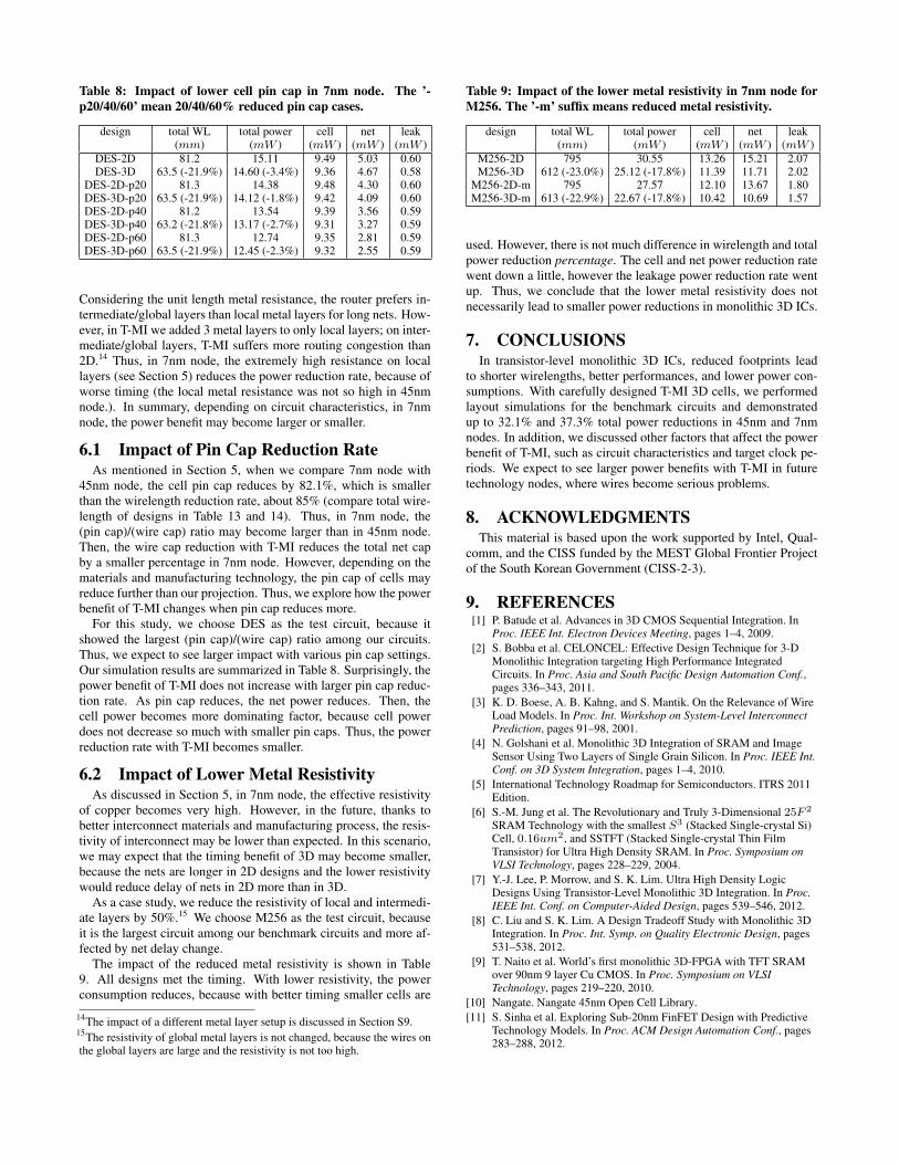
Table 8: Impact of lower cell pin cap in 7nm node. The ’-p20/40/60’ mean 20/40/60% reduced pin cap cases.
design total WL total power cell net leak(mm) (mW ) (mW ) (mW ) (mW )
DES-2D 81.2 15.11 9.49 5.03 0.60DES-3D 63.5 (-21.9%) 14.60 (-3.4%) 9.36 4.67 0.58
DES-2D-p20 81.3 14.38 9.48 4.30 0.60DES-3D-p20 63.5 (-21.9%) 14.12 (-1.8%) 9.42 4.09 0.60DES-2D-p40 81.2 13.54 9.39 3.56 0.59DES-3D-p40 63.2 (-21.8%) 13.17 (-2.7%) 9.31 3.27 0.59DES-2D-p60 81.3 12.74 9.35 2.81 0.59DES-3D-p60 63.5 (-21.9%) 12.45 (-2.3%) 9.32 2.55 0.59
Considering the unit length metal resistance, the router prefers in-termediate/global layers than local metal layers for long nets. How-ever, in T-MI we added 3 metal layers to only local layers; on inter-mediate/global layers, T-MI suffers more routing congestion than2D.14 Thus, in 7nm node, the extremely high resistance on locallayers (see Section 5) reduces the power reduction rate, because ofworse timing (the local metal resistance was not so high in 45nmnode.). In summary, depending on circuit characteristics, in 7nmnode, the power benefit may become larger or smaller.
6.1 Impact of Pin Cap Reduction RateAs mentioned in Section 5, when we compare 7nm node with
45nm node, the cell pin cap reduces by 82.1%, which is smallerthan the wirelength reduction rate, about 85% (compare total wire-length of designs in Table 13 and 14). Thus, in 7nm node, the(pin cap)/(wire cap) ratio may become larger than in 45nm node.Then, the wire cap reduction with T-MI reduces the total net capby a smaller percentage in 7nm node. However, depending on thematerials and manufacturing technology, the pin cap of cells mayreduce further than our projection. Thus, we explore how the powerbenefit of T-MI changes when pin cap reduces more.
For this study, we choose DES as the test circuit, because itshowed the largest (pin cap)/(wire cap) ratio among our circuits.Thus, we expect to see larger impact with various pin cap settings.Our simulation results are summarized in Table 8. Surprisingly, thepower benefit of T-MI does not increase with larger pin cap reduc-tion rate. As pin cap reduces, the net power reduces. Then, thecell power becomes more dominating factor, because cell powerdoes not decrease so much with smaller pin caps. Thus, the powerreduction rate with T-MI becomes smaller.
6.2 Impact of Lower Metal ResistivityAs discussed in Section 5, in 7nm node, the effective resistivity
of copper becomes very high. However, in the future, thanks tobetter interconnect materials and manufacturing process, the resis-tivity of interconnect may be lower than expected. In this scenario,we may expect that the timing benefit of 3D may become smaller,because the nets are longer in 2D designs and the lower resistivitywould reduce delay of nets in 2D more than in 3D.
As a case study, we reduce the resistivity of local and intermedi-ate layers by 50%.15 We choose M256 as the test circuit, becauseit is the largest circuit among our benchmark circuits and more af-fected by net delay change.
The impact of the reduced metal resistivity is shown in Table9. All designs met the timing. With lower resistivity, the powerconsumption reduces, because with better timing smaller cells are
14The impact of a different metal layer setup is discussed in Section S9.15The resistivity of global metal layers is not changed, because the wires onthe global layers are large and the resistivity is not too high.
Table 9: Impact of the lower metal resistivity in 7nm node forM256. The ’-m’ suffix means reduced metal resistivity.
design total WL total power cell net leak(mm) (mW ) (mW ) (mW ) (mW )
M256-2D 795 30.55 13.26 15.21 2.07M256-3D 612 (-23.0%) 25.12 (-17.8%) 11.39 11.71 2.02
M256-2D-m 795 27.57 12.10 13.67 1.80M256-3D-m 613 (-22.9%) 22.67 (-17.8%) 10.42 10.69 1.57
used. However, there is not much difference in wirelength and totalpower reduction percentage. The cell and net power reduction ratewent down a little, however the leakage power reduction rate wentup. Thus, we conclude that the lower metal resistivity does notnecessarily lead to smaller power reductions in monolithic 3D ICs.
7. CONCLUSIONSIn transistor-level monolithic 3D ICs, reduced footprints lead
to shorter wirelengths, better performances, and lower power con-sumptions. With carefully designed T-MI 3D cells, we performedlayout simulations for the benchmark circuits and demonstratedup to 32.1% and 37.3% total power reductions in 45nm and 7nmnodes. In addition, we discussed other factors that affect the powerbenefit of T-MI, such as circuit characteristics and target clock pe-riods. We expect to see larger power benefits with T-MI in futuretechnology nodes, where wires become serious problems.
8. ACKNOWLEDGMENTSThis material is based upon the work supported by Intel, Qual-
comm, and the CISS funded by the MEST Global Frontier Projectof the South Korean Government (CISS-2-3).
9. REFERENCES[1] P. Batude et al. Advances in 3D CMOS Sequential Integration. In
Proc. IEEE Int. Electron Devices Meeting, pages 1–4, 2009.[2] S. Bobba et al. CELONCEL: Effective Design Technique for 3-D
Monolithic Integration targeting High Performance IntegratedCircuits. In Proc. Asia and South Pacific Design Automation Conf.,pages 336–343, 2011.
[3] K. D. Boese, A. B. Kahng, and S. Mantik. On the Relevance of WireLoad Models. In Proc. Int. Workshop on System-Level InterconnectPrediction, pages 91–98, 2001.
[4] N. Golshani et al. Monolithic 3D Integration of SRAM and ImageSensor Using Two Layers of Single Grain Silicon. In Proc. IEEE Int.Conf. on 3D System Integration, pages 1–4, 2010.
[5] International Technology Roadmap for Semiconductors. ITRS 2011Edition.
[6] S.-M. Jung et al. The Revolutionary and Truly 3-Dimensional 25F 2
SRAM Technology with the smallest S3 (Stacked Single-crystal Si)Cell, 0.16um2, and SSTFT (Stacked Single-crystal Thin FilmTransistor) for Ultra High Density SRAM. In Proc. Symposium onVLSI Technology, pages 228–229, 2004.
[7] Y.-J. Lee, P. Morrow, and S. K. Lim. Ultra High Density LogicDesigns Using Transistor-Level Monolithic 3D Integration. In Proc.IEEE Int. Conf. on Computer-Aided Design, pages 539–546, 2012.
[8] C. Liu and S. K. Lim. A Design Tradeoff Study with Monolithic 3DIntegration. In Proc. Int. Symp. on Quality Electronic Design, pages531–538, 2012.
[9] T. Naito et al. World’s first monolithic 3D-FPGA with TFT SRAMover 90nm 9 layer Cu CMOS. In Proc. Symposium on VLSITechnology, pages 219–220, 2010.
[10] Nangate. Nangate 45nm Open Cell Library.[11] S. Sinha et al. Exploring Sub-20nm FinFET Design with Predictive
Technology Models. In Proc. ACM Design Automation Conf., pages283–288, 2012.
(a) INV (b) NAND2
(d) DFF
(c) MUX2
top
tier
bot
tier
NMOS
PMOS
MIVdirect
S/D
contact
Figure 5: GDSII layouts of our T-MI cells. The S/D meanssource/drain. The p/nwell and implants are not shown for sim-plicity.
0 5 10 15 20
0
100
200
300
400
wirele
ngth
(um
)
fanout
FPU AES LDPC DES M256
Figure 6: Fanout vs. wirelength in 2D wire load models.
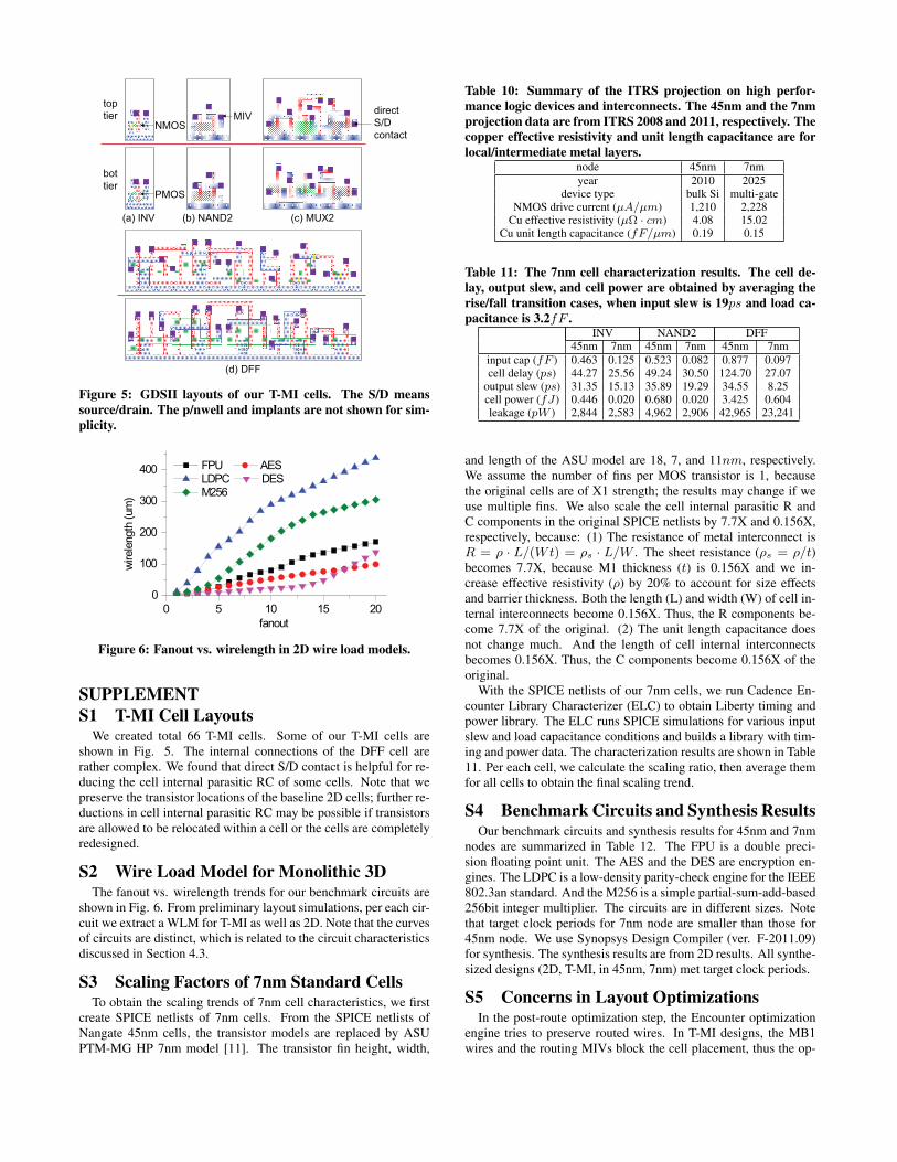
SUPPLEMENTS1 T-MI Cell Layouts
We created total 66 T-MI cells. Some of our T-MI cells areshown in Fig. 5. The internal connections of the DFF cell arerather complex. We found that direct S/D contact is helpful for re-ducing the cell internal parasitic RC of some cells. Note that wepreserve the transistor locations of the baseline 2D cells; further re-ductions in cell internal parasitic RC may be possible if transistorsare allowed to be relocated within a cell or the cells are completelyredesigned.
S2 Wire Load Model for Monolithic 3DThe fanout vs. wirelength trends for our benchmark circuits are
shown in Fig. 6. From preliminary layout simulations, per each cir-cuit we extract a WLM for T-MI as well as 2D. Note that the curvesof circuits are distinct, which is related to the circuit characteristicsdiscussed in Section 4.3.
S3 Scaling Factors of 7nm Standard CellsTo obtain the scaling trends of 7nm cell characteristics, we first
create SPICE netlists of 7nm cells. From the SPICE netlists ofNangate 45nm cells, the transistor models are replaced by ASUPTM-MG HP 7nm model [11]. The transistor fin height, width,
Table 10: Summary of the ITRS projection on high perfor-mance logic devices and interconnects. The 45nm and the 7nmprojection data are from ITRS 2008 and 2011, respectively. Thecopper effective resistivity and unit length capacitance are forlocal/intermediate metal layers.
node 45nm 7nmyear 2010 2025
device type bulk Si multi-gateNMOS drive current (µA/µm) 1,210 2,228
Cu effective resistivity (µΩ · cm) 4.08 15.02Cu unit length capacitance (fF/µm) 0.19 0.15
Table 11: The 7nm cell characterization results. The cell de-lay, output slew, and cell power are obtained by averaging therise/fall transition cases, when input slew is 19ps and load ca-pacitance is 3.2fF .
INV NAND2 DFF45nm 7nm 45nm 7nm 45nm 7nm
input cap (fF ) 0.463 0.125 0.523 0.082 0.877 0.097cell delay (ps) 44.27 25.56 49.24 30.50 124.70 27.07
output slew (ps) 31.35 15.13 35.89 19.29 34.55 8.25cell power (fJ) 0.446 0.020 0.680 0.020 3.425 0.604leakage (pW ) 2,844 2,583 4,962 2,906 42,965 23,241
and length of the ASU model are 18, 7, and 11nm, respectively.We assume the number of fins per MOS transistor is 1, becausethe original cells are of X1 strength; the results may change if weuse multiple fins. We also scale the cell internal parasitic R andC components in the original SPICE netlists by 7.7X and 0.156X,respectively, because: (1) The resistance of metal interconnect isR = ρ · L/(Wt) = ρs · L/W . The sheet resistance (ρs = ρ/t)becomes 7.7X, because M1 thickness (t) is 0.156X and we in-crease effective resistivity (ρ) by 20% to account for size effectsand barrier thickness. Both the length (L) and width (W) of cell in-ternal interconnects become 0.156X. Thus, the R components be-come 7.7X of the original. (2) The unit length capacitance doesnot change much. And the length of cell internal interconnectsbecomes 0.156X. Thus, the C components become 0.156X of theoriginal.
With the SPICE netlists of our 7nm cells, we run Cadence En-counter Library Characterizer (ELC) to obtain Liberty timing andpower library. The ELC runs SPICE simulations for various inputslew and load capacitance conditions and builds a library with tim-ing and power data. The characterization results are shown in Table11. Per each cell, we calculate the scaling ratio, then average themfor all cells to obtain the final scaling trend.
S4 Benchmark Circuits and Synthesis ResultsOur benchmark circuits and synthesis results for 45nm and 7nm
nodes are summarized in Table 12. The FPU is a double preci-sion floating point unit. The AES and the DES are encryption en-gines. The LDPC is a low-density parity-check engine for the IEEE802.3an standard. And the M256 is a simple partial-sum-add-based256bit integer multiplier. The circuits are in different sizes. Notethat target clock periods for 7nm node are smaller than those for45nm node. We use Synopsys Design Compiler (ver. F-2011.09)for synthesis. The synthesis results are from 2D results. All synthe-sized designs (2D, T-MI, in 45nm, 7nm) met target clock periods.
S5 Concerns in Layout OptimizationsIn the post-route optimization step, the Encounter optimization
engine tries to preserve routed wires. In T-MI designs, the MB1wires and the routing MIVs block the cell placement, thus the op-

Table 12: Benchmark circuits and synthesis results.FPU AES LDPC DES M256
45nm nodetarget clock period (ns) 1.8 0.8 2.4 1.0 2.4
#cells 9,694 13,891 38,289 51,162 202,877cell area (µm2) 19,123 16,756 60,590 85,526 293,636
#nets 11,345 14,218 44,153 54,724 222,569average fanout 2.35 2.40 2.38 2.33 2.23
7nm nodetarget clock period (ns) 0.72 0.27 0.9 0.3 1.0
#cells 11,378 12,541 37,322 50,833 191,543cell area (µm2) 447.1 362.3 1456.4 2061.3 6788.8
#nets 12,484 12,811 43,183 54,426 209,545average fanout 2.44 2.57 2.41 2.33 2.30
VDD/VSS
MIV
cells cannot be placed
MB1 MB1
M1
VDD/VSS
Figure 7: A zoom-in shot of T-MI design for AES. Skyblue rect-angles are standard cells. For clarity, only MB1, M1, and MIVlayers are shown.
timizer cannot place cells at (nor move cells to) such places. Forexample, in Fig. 7, the white spaces (dotted boxes) cannot be usedfor optimization such as buffering or gate sizing.
To see whether these MIV/MB1 blockages cause design qualitydegradation, we perform a layout simulation. For this case study,we use AES as the target circuit, because it showed a high place-ment utilization with lots of densely packed placement regions.From layout simulations, we observe that there are negligible dif-ferences in design quality, in terms of wirelength (+0.1%), timing(WNS = +25ps in original vs. +21ps without MB1 and MIV), andtotal power (-0.1%). Thus, we conclude that under our settings(placement, routing, optimization options, final utilization, etc.),the routings on MB1 and MIV do not degrade design quality no-ticeably. Note that the utilization of the above AES design is around80%; we may see problems caused by the MIV/MB1 blockageswhen utilization is very high. However, in general, it is customarynot to exceed the 80% utilization, due to various reasons (place-ment and routing quality, optimization quality, decap area, etc).
S6 Detailed Layout ResultsThe detailed layout simulation results for 45nm node are shown
in Table 13. We set the target utilization to around 80%, which iscommon in industry designs. Since we observed severe wire con-gestions in LDPC (see Fig. 3(a)), the target utilization was loweredto about 33%; the 2D design was barely routable with this setting.We also observed significant wire congestions in M256, thus the
Table 15: Layout results with/without our T-MI WLMs. The’-n’ suffix means without our T-MI WLM.
design total WL WNS total power(mm) (ps) (mW )
FPU-3D 149.1 +4 7.22FPU-3D-n 152.0 (+1.9%) +11 7.20 (-0.3%)AES-3D 198.8 +25 12.20
AES-3D-n 199.0 (+0.1%) +21 12.19 (-0.1%)LDPC-3D 2527.8 +12 37.22
LDPC-3D-n 2782.2 (+10.1%) +16 40.99 (+10.1%)DES-3D 479.1 +32 61.24
DES-3D-n 481.7 (+0.5%) +29 61.79 (+0.9%)M256-3D 4760.2 0 160.5
M256-3D-n 5020.6 (+5.5%) +3 166.8 (+3.9%)
Table 16: Wire vs. pin capacitance breakdown of LDPC andDES in 45nm node. The values are for the entire circuit.
design total cap. (pF ) power (mW )wire pin wire pin
LDPC-2D 558.0 134.4 30.73 9.04LDPC-3D 310.3 123.6 15.88 8.32DES-2D 64.4 127.4 8.88 17.80DES-3D 50.1 126.6 6.87 17.76
target utilization was lowered to 68%. All designs met the timing(WNS≥0).
The detailed layout simulation results for 7nm node are shownin Table 14. We set similar target utilizations as for 45nm node. Alldesigns met timing.
S7 Impact of T-MI Wire Load ModelAs mentioned in Section 3.4, we create custom WLMs for T-MI
designs. There have been debates on whether WLM is helpful ornot to the final layout results [3]. Since our target circuits are smallto medium sized, we may expect that WLM is helpful to some ex-tent. To see the impact of the custom WLMs on design quality, weperform the synthesis for T-MI designs with not our T-MI WLMsbut the 2D WLMs. As a result, the synthesized netlists for T-MIand 2D become similar. The layout results with/without customWLM for T-MI designs are shown in Table 15. For FPU, AES,and DES, the design quality difference is negligible. However, forLDPC and M256, we observe significant increase in wirelength andtotal power without T-MI WLM. Thus, we conclude that for somedesigns, T-MI WLM models are helpful for obtaining larger powerbenefits with T-MI.
S8 Breakdown of Net PowerWe break net power into wire and pin power components (net =
wire + pin). Wire means metal wires and vias used for connect-ing cell pins, and pin means input pins of cells. As shown in Ta-ble 16, in LDPC, wire cap is much larger than pin cap, and so iswire power. Most of the net power reduction is from reduced wire-lengths, as seen by the wire power reduction. In contrast, in DES,pin cap is much larger than wire cap. Thus, reduced wirelengthsand wire power only reduces a small portion of the net power. Infact, most of the nets in DES are short, whereas most are longin LDPC; the average wirelength of LDPC-2D and DES-2D are72.0µm and 10.5µm, respectively.
S9 Impact of the Metal Layer SetupTo see the impact of the metal layer setup on power benefit of
T-MI, we modify the metal layer stack of T-MI. Instead of adding3 local metal layers on the top tier, we add 2 to local and 2 tointermediate metal layers. The original and modified metal stacks
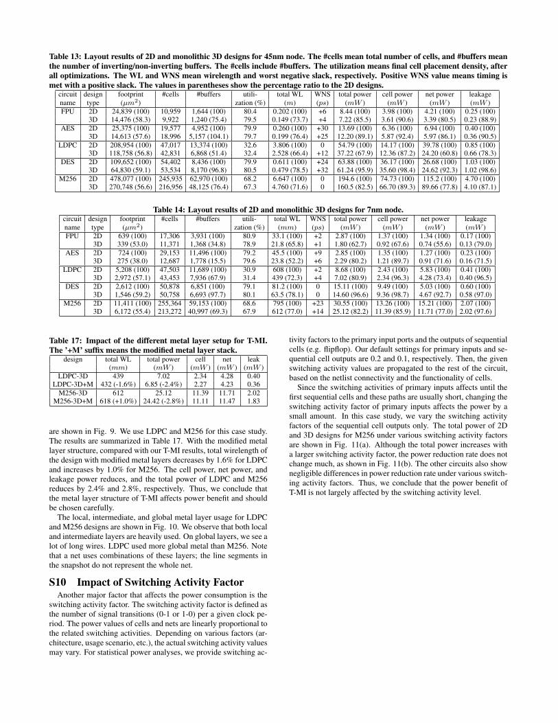
Table 13: Layout results of 2D and monolithic 3D designs for 45nm node. The #cells mean total number of cells, and #buffers meanthe number of inverting/non-inverting buffers. The #cells include #buffers. The utilization means final cell placement density, afterall optimizations. The WL and WNS mean wirelength and worst negative slack, respectively. Positive WNS value means timing ismet with a positive slack. The values in parentheses show the percentage ratio to the 2D designs.
circuit design footprint #cells #buffers utili- total WL WNS total power cell power net power leakagename type (µm2) zation (%) (m) (ps) (mW ) (mW ) (mW ) (mW )FPU 2D 24,839 (100) 10,959 1,644 (100) 80.4 0.202 (100) +6 8.44 (100) 3.98 (100) 4.21 (100) 0.25 (100)
3D 14,476 (58.3) 9,922 1,240 (75.4) 79.5 0.149 (73.7) +4 7.22 (85.5) 3.61 (90.6) 3.39 (80.5) 0.23 (88.9)AES 2D 25,375 (100) 19,577 4,952 (100) 79.9 0.260 (100) +30 13.69 (100) 6.36 (100) 6.94 (100) 0.40 (100)
3D 14,613 (57.6) 18,996 5,157 (104.1) 79.7 0.199 (76.4) +25 12.20 (89.1) 5.87 (92.4) 5.97 (86.1) 0.36 (90.5)LDPC 2D 208,954 (100) 47,017 13,374 (100) 32.6 3.806 (100) 0 54.79 (100) 14.17 (100) 39.78 (100) 0.85 (100)
3D 118,758 (56.8) 42,831 6,868 (51.4) 32.4 2.528 (66.4) +12 37.22 (67.9) 12.36 (87.2) 24.20 (60.8) 0.66 (78.3)DES 2D 109,652 (100) 54,402 8,436 (100) 79.9 0.611 (100) +24 63.88 (100) 36.17 (100) 26.68 (100) 1.03 (100)
3D 64,830 (59.1) 53,534 8,170 (96.8) 80.5 0.479 (78.5) +32 61.24 (95.9) 35.60 (98.4) 24.62 (92.3) 1.02 (98.6)M256 2D 478,077 (100) 245,935 62,970 (100) 68.2 6.647 (100) 0 194.6 (100) 74.73 (100) 115.2 (100) 4.70 (100)
3D 270,748 (56.6) 216,956 48,125 (76.4) 67.3 4.760 (71.6) 0 160.5 (82.5) 66.70 (89.3) 89.66 (77.8) 4.10 (87.1)
Table 14: Layout results of 2D and monolithic 3D designs for 7nm node.circuit design footprint #cells #buffers utili- total WL WNS total power cell power net power leakagename type (µm2) zation (%) (mm) (ps) (mW ) (mW ) (mW ) (mW )FPU 2D 639 (100) 17,306 3,931 (100) 80.9 33.1 (100) +2 2.87 (100) 1.37 (100) 1.34 (100) 0.17 (100)
3D 339 (53.0) 11,371 1,368 (34.8) 78.9 21.8 (65.8) +1 1.80 (62.7) 0.92 (67.6) 0.74 (55.6) 0.13 (79.0)AES 2D 724 (100) 29,153 11,496 (100) 79.2 45.5 (100) +9 2.85 (100) 1.35 (100) 1.27 (100) 0.23 (100)
3D 275 (38.0) 12,687 1,778 (15.5) 79.6 23.8 (52.2) +6 2.29 (80.2) 1.21 (89.7) 0.91 (71.6) 0.16 (71.5)LDPC 2D 5,208 (100) 47,503 11,689 (100) 30.9 608 (100) +2 8.68 (100) 2.43 (100) 5.83 (100) 0.41 (100)
3D 2,972 (57.1) 43,453 7,936 (67.9) 31.4 439 (72.3) +4 7.02 (80.9) 2.34 (96.3) 4.28 (73.4) 0.40 (96.5)DES 2D 2,612 (100) 50,878 6,851 (100) 79.1 81.2 (100) 0 15.11 (100) 9.49 (100) 5.03 (100) 0.60 (100)
3D 1,546 (59.2) 50,758 6,693 (97.7) 80.1 63.5 (78.1) 0 14.60 (96.6) 9.36 (98.7) 4.67 (92.7) 0.58 (97.0)M256 2D 11,411 (100) 255,364 59,153 (100) 68.6 795 (100) +23 30.55 (100) 13.26 (100) 15.21 (100) 2.07 (100)
3D 6,172 (55.4) 213,272 40,997 (69.3) 67.9 612 (77.0) +14 25.12 (82.2) 11.39 (85.9) 11.71 (77.0) 2.02 (97.6)
Table 17: Impact of the different metal layer setup for T-MI.The ’+M’ suffix means the modified metal layer stack.
design total WL total power cell net leak(mm) (mW ) (mW ) (mW ) (mW )
LDPC-3D 439 7.02 2.34 4.28 0.40LDPC-3D+M 432 (-1.6%) 6.85 (-2.4%) 2.27 4.23 0.36
M256-3D 612 25.12 11.39 11.71 2.02M256-3D+M 618 (+1.0%) 24.42 (-2.8%) 11.11 11.47 1.83
are shown in Fig. 9. We use LDPC and M256 for this case study.The results are summarized in Table 17. With the modified metallayer structure, compared with our T-MI results, total wirelength ofthe design with modified metal layers decreases by 1.6% for LDPCand increases by 1.0% for M256. The cell power, net power, andleakage power reduces, and the total power of LDPC and M256reduces by 2.4% and 2.8%, respectively. Thus, we conclude thatthe metal layer structure of T-MI affects power benefit and shouldbe chosen carefully.
The local, intermediate, and global metal layer usage for LDPCand M256 designs are shown in Fig. 10. We observe that both localand intermediate layers are heavily used. On global layers, we see alot of long wires. LDPC used more global metal than M256. Notethat a net uses combinations of these layers; the line segments inthe snapshot do not represent the whole net.
S10 Impact of Switching Activity FactorAnother major factor that affects the power consumption is the
switching activity factor. The switching activity factor is defined asthe number of signal transitions (0-1 or 1-0) per a given clock pe-riod. The power values of cells and nets are linearly proportional tothe related switching activities. Depending on various factors (ar-chitecture, usage scenario, etc.), the actual switching activity valuesmay vary. For statistical power analyses, we provide switching ac-
tivity factors to the primary input ports and the outputs of sequentialcells (e.g. flipflop). Our default settings for primary inputs and se-quential cell outputs are 0.2 and 0.1, respectively. Then, the givenswitching activity values are propagated to the rest of the circuit,based on the netlist connectivity and the functionality of cells.
Since the switching activities of primary inputs affects until thefirst sequential cells and these paths are usually short, changing theswitching activity factor of primary inputs affects the power by asmall amount. In this case study, we vary the switching activityfactors of the sequential cell outputs only. The total power of 2Dand 3D designs for M256 under various switching activity factorsare shown in Fig. 11(a). Although the total power increases witha larger switching activity factor, the power reduction rate does notchange much, as shown in Fig. 11(b). The other circuits also shownegligible differences in power reduction rate under various switch-ing activity factors. Thus, we conclude that the power benefit ofT-MI is not largely affected by the switching activity level.
(b) T-MI-placement(a) 2D-placement
(d) T-MI-routing(c) 2D-routing
170.53x168.24um
127.70x126.20um
Figure 8: The placement and routing snapshots of AES designs.The figures reflect the relative sizes of 2D vs. T-MI designs.
(a) 2D (b) T-MI (c) T-MI+M
local
inter-
mediate
global
M1-3
M4-6
M7-8
M1-6
M7-9
M10-11
MB1
M1-5
MB1
M6-10
M11-12
Figure 9: Metal layer stack diagrams for (a) 2D, (b) T-MI, and(c) T-MI+M. The ’+M’ means modified metal layer stack.
(a) LDPC (b) M256
global layers (M11-12)
intermediate layers (M6-10)
local layers (MB1, M1-5)
Figure 10: GDSII snapshots of local, intermediate, and globalmetal layers for (a) LDPC and (b) M256.
0.1 0.2 0.3 0.40
100
200
300
400
500
tota
l pow
er (m
W)
switching activity
M256-2D M256-3D
0.1 0.2 0.3 0.4
5
10
15
20
25
30
35
pow
er re
duct
ion (%
)
switching activity
FPU AES LDPC DES M256
(a) (b)
Figure 11: Power dependency on switching activity factor. (a)Total power of M256 with various switching activity factors,and (b) power reduction rate under various switching activityfactor. All results are from 45nm node.
Related Documents