Observation of High Resolution Microstructures in Thermal Sprayed Coatings and Single Deposited Splats Using Ion Beam Milling KeeHyun Kim 1; * , Makoto Watanabe 1 , Seiji Kuroda 1 and Naomi Kawano 2 1 Hybrid Materials Center, National Institute for Materials Science (NIMS), Tsukuba 305-0047, Japan 2 Materials Nanoarchitectonics Foundry, National Institute for Materials Science (NIMS), Tsukuba 305-0047, Japan We have investigated microstructures of thermal sprayed coatings and single deposited splats using two types of ion beam milling: one is broad argon ion beam for the cross-sectioning of thermal sprayed coatings in a cross section polisher and the other is focused gallium ion beam for the cross-sectioning and transmission electron microscopy (TEM) sample preparation of single splats. The cross section of tungsten carbide- cobalt (WC-Co) coatings fabricated by the polisher showed that it created a mirrored surface with minimized artifacts such as pull-outs of ceramic particles or smearings of pores which can be made by conventional metallographic preparations. A thin and locally re-thinned membrane of single nickel (Ni) splat was feasible to observe the internal interface of particle/substrate in high resolution atomic scale images. Substrate was heavily deformed by the impact of nickel particle with high kinetic and thermal energies. The particle and the substrate were intimately bonded without any voids or gaps. [doi:10.2320/matertrans.T-M2010826] (Received August 9, 2010; Accepted November 16, 2010; Published February 16, 2011) Keywords: sample preparation, ion milling, cross sectional polisher, focused ion beam, transmission electron microscopy 1. Introduction Cross sections of coated material layers are generally observed to know the porosity, inside microstructure and phase or composition analysis by optical microscope or scanning electron microscope (SEM). 1) Metallographic prep- aration of thermal sprayed coatings, however, is often problematic. Cross sections of ceramic coatings tend to exhibit exaggerated pores due to pull-outs of ceramic particles during grinding. Metallic coatings, on the other hand, tend to appear denser than the actual because very fine pores and unbonded boundaries between sprayed particles tend to be filled by plastic deformation of metals during grinding and polishing. Therefore, when a cross section of tungsten carbide-cobalt (WC-Co) cermet coatings composed of hard ceramics and relatively soft metal is prepared by conventional metallographic polishing the artifacts are boosted. To minimize such artifacts, the research reported herein used broad argon ion beam milling. When a broad beam of ions with maximum breadth of 500 mm 2) collides with atoms of a target material, the ions’ kinetic energy is transferred to surface atoms of the target. If the energy is larger than the sublimation energy of the surface atoms, 3) the atoms are sputtered away and consequently a clean surface can be created. A technique using the ion milling for preparation of polished cross sections was demonstrated with good quality of backscattered SEM image by the manufac- turer of a so-called cross-section polisher 4) and was applied for high spatial resolution electron probe X-ray microanalysis of an iron alloy. 2) In this study, the technique was used to make vertical cross sections of WC-Co coatings essentially free from the artifacts as well as a large viewing area. Another technique using ion beam for SEM and trans- mission electron microscopy (TEM) observations is focused gallium ion beam (FIB) milling. Since the first FIB system based on the field ionization of liquid gallium for microprobe applications was developed in 1970s, 5,6) it has been contin- uously evolved. 7–9) As a FIB milling technique facilitates delicate control of beam sizes under 10 nm with current densities of under 110 A/cm 2 at desired locations, 10) many researchers in thermal spray field have successfully used the FIB to investigate the cross sectional microstructures of isolated single splats, which are difficult by conventional metallographic preparations due to the splat size with micrometer scales, on substrate by SEM such as air plasma sprayed Ni-5% Al single splats, 11) high velocity oxy-fuel (HVOF) WC-Co splats, 12) high-powder hybrid plasma sprayed yittria-stabilized zirconia splats, 13) and cold sprayed aluminum splats. 14) Especially, a FIB apparatus with a micromanipulator can make directly a TEM membrane from an as-sprayed sample in its chamber without moving the sample or any mechanical sawing and thinning, 15,16) which are inevitable in conventional sample preparations such as electro-chemical jet polishing, micro-cleaving and dimpling method. 17–20) Many researchers hence have made TEM samples by the FIB method from micron-sized powders or small splats or thick coating layers at a desired location. 1,21–29) Because the FIB is an imaging tool in its own right as well as the milling and thinning capability in sample preparation, 30) during the FIB fabrication, one can check the milling state and get images of the sample. TEM samples normally have wedge-shape, i.e. top surface is the thinnest region and the inside is much thicker. 16) Therefore, when observing a thermal-sprayed splat from the surface to the interface of splat/substrate with TEM, it is quite difficult to obtain high resolution atomic structure images near the interface of splat/substrate because the region is too thick to derive the atomic structure. 1,21–24) For the high resolution images, several researchers prepared firstly the cross section of a single splat by a conventional polishing method using silicon carbide (SiC) papers or the FIB method and then, from the cross section, several TEM samples were made respectively at desired locations within the single splat. 27–29) Once a TEM sample was made and * Corresponding author, E-mail: [email protected] Materials Transactions, Vol. 52, No. 3 (2011) pp. 439 to 446 #2011 Japan Thermal Spray Society

Welcome message from author
This document is posted to help you gain knowledge. Please leave a comment to let me know what you think about it! Share it to your friends and learn new things together.
Transcript
Observation of High Resolution Microstructures in Thermal Sprayed Coatings
and Single Deposited Splats Using Ion Beam Milling
KeeHyun Kim1;*, Makoto Watanabe1, Seiji Kuroda1 and Naomi Kawano2
1Hybrid Materials Center, National Institute for Materials Science (NIMS), Tsukuba 305-0047, Japan2Materials Nanoarchitectonics Foundry, National Institute for Materials Science (NIMS), Tsukuba 305-0047, Japan
We have investigated microstructures of thermal sprayed coatings and single deposited splats using two types of ion beam milling: one isbroad argon ion beam for the cross-sectioning of thermal sprayed coatings in a cross section polisher and the other is focused gallium ion beamfor the cross-sectioning and transmission electron microscopy (TEM) sample preparation of single splats. The cross section of tungsten carbide-cobalt (WC-Co) coatings fabricated by the polisher showed that it created a mirrored surface with minimized artifacts such as pull-outs ofceramic particles or smearings of pores which can be made by conventional metallographic preparations. A thin and locally re-thinnedmembrane of single nickel (Ni) splat was feasible to observe the internal interface of particle/substrate in high resolution atomic scale images.Substrate was heavily deformed by the impact of nickel particle with high kinetic and thermal energies. The particle and the substrate wereintimately bonded without any voids or gaps. [doi:10.2320/matertrans.T-M2010826]
(Received August 9, 2010; Accepted November 16, 2010; Published February 16, 2011)
Keywords: sample preparation, ion milling, cross sectional polisher, focused ion beam, transmission electron microscopy
1. Introduction
Cross sections of coated material layers are generallyobserved to know the porosity, inside microstructure andphase or composition analysis by optical microscope orscanning electron microscope (SEM).1) Metallographic prep-aration of thermal sprayed coatings, however, is oftenproblematic. Cross sections of ceramic coatings tend toexhibit exaggerated pores due to pull-outs of ceramicparticles during grinding. Metallic coatings, on the otherhand, tend to appear denser than the actual because very finepores and unbonded boundaries between sprayed particlestend to be filled by plastic deformation of metals duringgrinding and polishing. Therefore, when a cross section oftungsten carbide-cobalt (WC-Co) cermet coatings composedof hard ceramics and relatively soft metal is prepared byconventional metallographic polishing the artifacts areboosted. To minimize such artifacts, the research reportedherein used broad argon ion beam milling. When a broadbeam of ions with maximum breadth of 500 mm2) collideswith atoms of a target material, the ions’ kinetic energy istransferred to surface atoms of the target. If the energy islarger than the sublimation energy of the surface atoms,3) theatoms are sputtered away and consequently a clean surfacecan be created. A technique using the ion milling forpreparation of polished cross sections was demonstrated withgood quality of backscattered SEM image by the manufac-turer of a so-called cross-section polisher4) and was appliedfor high spatial resolution electron probe X-ray microanalysisof an iron alloy.2) In this study, the technique was used tomake vertical cross sections of WC-Co coatings essentiallyfree from the artifacts as well as a large viewing area.
Another technique using ion beam for SEM and trans-mission electron microscopy (TEM) observations is focusedgallium ion beam (FIB) milling. Since the first FIB systembased on the field ionization of liquid gallium for microprobe
applications was developed in 1970s,5,6) it has been contin-uously evolved.7–9) As a FIB milling technique facilitatesdelicate control of beam sizes under 10 nm with currentdensities of under 1�10A/cm2 at desired locations,10) manyresearchers in thermal spray field have successfully usedthe FIB to investigate the cross sectional microstructures ofisolated single splats, which are difficult by conventionalmetallographic preparations due to the splat size withmicrometer scales, on substrate by SEM such as air plasmasprayed Ni-5% Al single splats,11) high velocity oxy-fuel(HVOF) WC-Co splats,12) high-powder hybrid plasmasprayed yittria-stabilized zirconia splats,13) and cold sprayedaluminum splats.14) Especially, a FIB apparatus with amicromanipulator can make directly a TEM membrane froman as-sprayed sample in its chamber without moving thesample or any mechanical sawing and thinning,15,16) whichare inevitable in conventional sample preparations such aselectro-chemical jet polishing, micro-cleaving and dimplingmethod.17–20) Many researchers hence have made TEMsamples by the FIB method from micron-sized powdersor small splats or thick coating layers at a desiredlocation.1,21–29) Because the FIB is an imaging tool in itsown right as well as the milling and thinning capability insample preparation,30) during the FIB fabrication, one cancheck the milling state and get images of the sample.
TEM samples normally have wedge-shape, i.e. top surfaceis the thinnest region and the inside is much thicker.16)
Therefore, when observing a thermal-sprayed splat fromthe surface to the interface of splat/substrate with TEM,it is quite difficult to obtain high resolution atomic structureimages near the interface of splat/substrate because theregion is too thick to derive the atomic structure.1,21–24) Forthe high resolution images, several researchers preparedfirstly the cross section of a single splat by a conventionalpolishing method using silicon carbide (SiC) papers or theFIB method and then, from the cross section, several TEMsamples were made respectively at desired locations withinthe single splat.27–29) Once a TEM sample was made and*Corresponding author, E-mail: [email protected]
Materials Transactions, Vol. 52, No. 3 (2011) pp. 439 to 446#2011 Japan Thermal Spray Society
observed, it is generally impossible to prepare much thinnersample at the desired position. By the FIB milling, however,it is possible to conduct re-thinning at any interested regioneven after TEM samples were already observed by electronmicroscopes. Best of all, the re-thinning technique enablesone to avoid making several TEM samples from a crosssection of single splat to obtain the high resolution images.
In this study, we have used two types of ion beam millingtechniques to investigate the microstructures of thermalsprayed coatings and single deposited splats and the bondingmechanism of sprayed particles and substrate: (i) broad argonion beam for SEM observations and (ii) focused galliumion beam for TEM observations of thermal sprayed splats,respectively. Examples are presented for HVOF cermetcoatings and warm sprayed metal. In addition, a local re-thinning technique using FIB for high resolution images ofthe interface of splat and substrate has been first introducedto derive the atomic structure.
2. Experimental Procedures
2.1 Feedstock material and sprayingCommercially available WC-Co powder (WC-12%Co,
Fujimi Inc., Japan) with an average carbide size of 0.2 mmand 12mass% cobalt contents was used to fabricate a coatingfor argon ion beam milling and SEM observations. TheWC-Co particles ranged from 15 to 45 mm powder size weresprayed onto a carbon steel substrate (JIS: S45C) via acommercial HVOF spraying equipment (JP5000, PraxairTechnology Inc., USA). The coating thickness was about300 mm. Details of used powder and spraying conditions forthe HVOF process are given elsewhere.31)
For FIB ion milling for TEM sample preparation,commercially available nickel powder (NI-914-3, PraxairTechnology Inc., USA) was used and sprayed on a mirror-polished S45C substrate with 5� 5� 5mm size via warmspraying process. Especially, single nickel splats were madeby the so-called wipe test at a minimum available powderfeeding rate of 4 g/min and with a rapid moving of the spraygun of 1500mm/s to eliminate secondary impacts by othernickel particles onto previously-deposited particles.32,33) Thespraying process to prepare single splats and coatings isdescribed in detail elsewhere.34,35) In the process, a mixtureof kerosene and oxygen ignited in a combustion chamber andwas mixed with nitrogen in a mixing chamber to lower itstemperature. Then, nickel powder was fed into the finalmixture of supersonic gases passing through a convergent-divergent nozzle. In this study, the nitrogen flow rate was1.5m3/min, which was an optimized condition to avoidmelting of sprayed particles and to make dense coating.
2.2 Cross-sectioning of coating layer by broad ion beammilling
Vertical cross-sections of HVOF sprayed WC-Co coatingswere prepared by a conventional mechanical polishing anda cross section polisher (SM-09020CP, JEOL, Japan),respectively. In the polisher, broad argon ion beam withmaximum breadth of 500 mm was used to mill the sample.The sample of 10� 5� 1:5mm was cut out from the as-sprayed specimen and lapped to have the uniform thickness.
Figure 1 shows a schematic illustration of the principle of thecross section polisher and an as-sprayed sample put on asample holder of the polisher. The molybdenum mask wasapplied to protect the sample surface except for the targetededge region where the argon beam would create the section.The accelerating voltage was 4 kV and the milling speed wasbelow 50 mm/h under the vacuum condition of 2� 10�3 Pa.In order to obtain a large and uniformly milled area, thesample was swung during milling.
Fig. 1 Schematic illustration of the principle of the cross section polisher
(a), an as-sprayed sample put on a sample holder (b) and in a CP (c).
Before argon ion beam milling, the molybdenum mask is put on the
sample.
440 K. Kim, M. Watanabe, S. Kuroda and N. Kawano
2.3 TEM sample preparation by focused ion beammilling
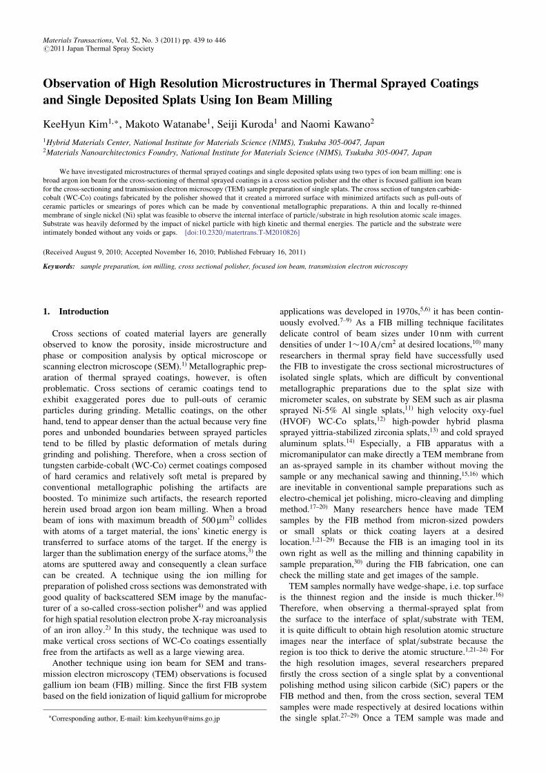
Thin enough membranes for TEM observation wereprepared from single splats deposited on steel substrate bya FIB milling equipment (FB-2100, Hitachi, Japan). Figure 2shows a schematic illustration of a typical FIB system and anas-sprayed sample put on a sample holder for FIB milling.
Figure 3 shows the 6-step specimen preparation procedureusing a FIB lift-out technique. Prior to the FIB crosssectioning, a strip of tungsten coating was deposited on thedesired location of as-sprayed single splat to protect thesurface from the ion beam milling and thinning. The beamvoltage and current are shown in Table 1. As the membranebecame thinner, a weaker beam was gradually applied toeliminate damage and deformation of the sample. Afterfinal milling, cleaning at a weak beam condition of 15 kVand 0.02 nA was conducted to remove or minimize a thinamorphous layer which is generally made by beam damage atthe surface of TEM specimen. At every cutting and thinningstage, images made by secondary electrons scattered bygallium ions were acquired to check the milling state andthickness of thin membrane. The scattered electrons aredetected and converted to photo signals by the scintillationdetector composed of a scintillator and a photomultipliertube.
Fig. 2 Schematic illustration of a typical FIB system (a), an as-sprayed
sample of 5� 5� 5mm size put on a sample holder for FIB milling (b)
and magnified image of copper grid part (c). Copper tape was used to fix
the as-sprayed sample on the holder. After FIB milling, a thin membrane
from the sample is put on the copper grid.
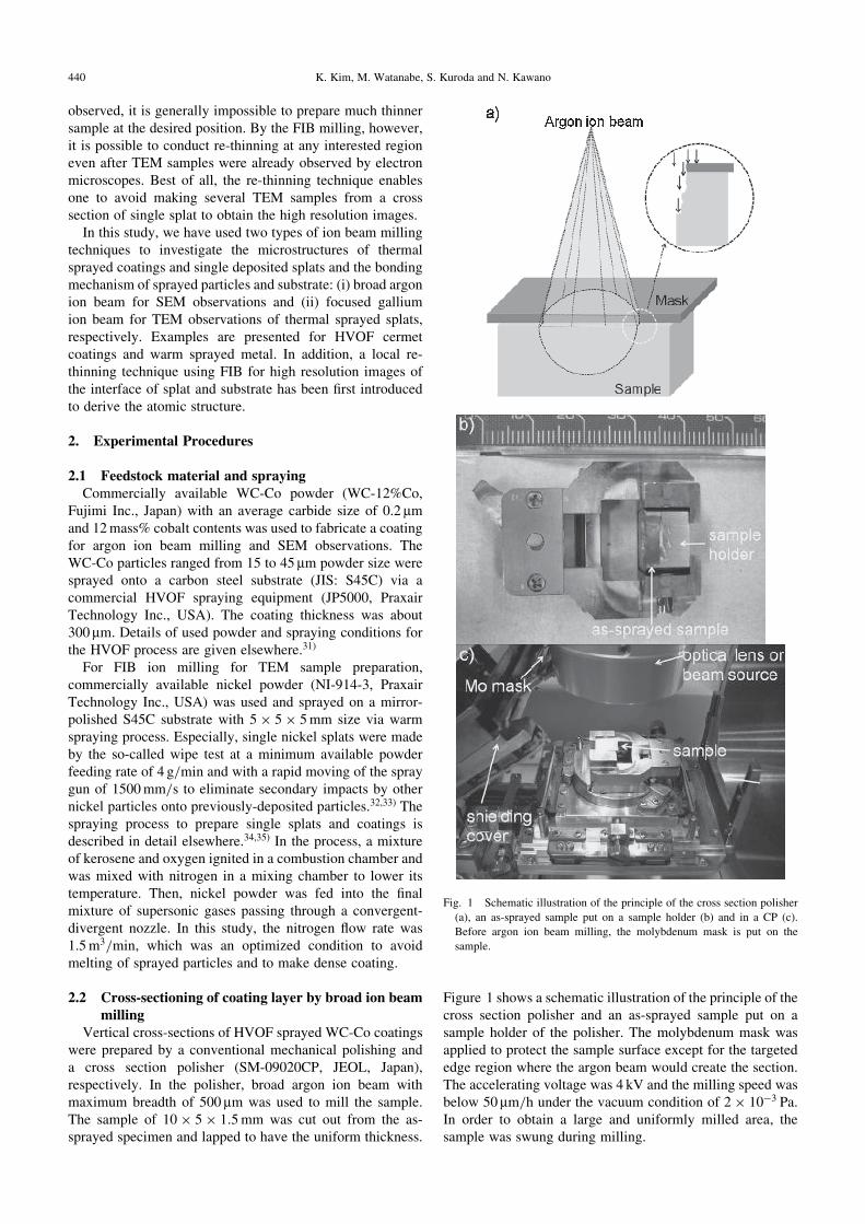
Fig. 3 A series of FIB lift-out technique for TEM sample preparation:
(a) tungsten deposition on a small area of 20� 5 mm at nickel particle
deposited on steel substrate, (b) making gradual trenches near the tungsten
deposited area, (c) 45� tilting of the specimen and bottom cutting,
(d) lifting-out of the specimen after a manipulator was connected on the
specimen by tungsten deposition and the remained left-side of panel (c)
was cut, (e) putting the specimen on a copper grid and cutting the bridge of
manipulator and specimen, and (f) after additional milling and cleaning on
the copper grid a TEM sample with an electron transparent area of about
7mm in length was made (see Fig. 5).
Observation of High Resolution Microstructures in Thermal Sprayed Coatings and Single Deposited Splats Using Ion Beam Milling 441
2.4 Re-thinning of TEM sampleA thin membrane of a single nickel splat made by the FIB
using a lift-out technology was re-thinned after it had beenobserved by TEM, which would be explained in section 3.3in detail. For the re-thinning, the TEM specimen was re-puton the sample holder that was already shown in Fig. 2. Then,the specimen was locally re-thinned at the desired positionsby the FIB milling. The beam conditions for the re-thinningwere 30 kV and 0:01�0:07 nA (step 4�6 in Table 1). Then,final cleaning at a weak beam condition of 15 kV and 0:01�0:04 nA was also conducted.
2.5 Microstructural analysisThe cross sections made by the conventional mechanical
polishing and the argon ion broad beam milling wereinvestigated by a field emission SEM (FE-SEM, JSM-6500,JEOL, Japan). The thin membranes made by the FIB processwere observed for high resolution images at the interfaceof splat and substrate by a FE-TEM (JEM-2100F, JEOL,Japan) with a scanning mode at an applied voltage of 200KV.Prior to the observation, the membrane was ion-cleaned byan ion cleaner (JIC-410, JEOL, Japan) to remove contami-nations such as hydrocarbons on the TEM specimen.
3. Results and Discussion
3.1 Comparison of microstructures of WC-Co coatingsprepared by two different polishing methods
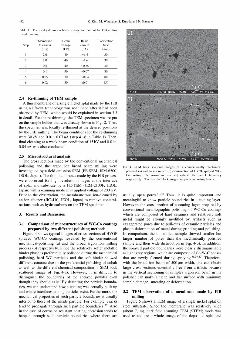
Figure 4 shows typical images of cross sections of HVOFsprayed WC-Co coatings revealed by the conventionalmechanical-polishing (a) and the broad argon ion millingprocess (b) respectively. Since the relatively softer metallicbinder phase is preferentially polished during the mechanicalpolishing, hard WC particles and the soft binder showeddifferent contrast due to the preferential polishing of cobaltas well as the different chemical composition in SEM backscattered image of Fig. 4(a). However, it is difficult todistinguish the boundaries of the sprayed powder eventhough they should exist. By detecting the particle bounda-ries, we can understand how a coating was actually built upand where interfaces among particles exist. Furthermore, themechanical properties of such particle boundaries is usuallyinferior to those of the inside particle. For example, crackstend to propagate through such particle boundaries.36) Alsoin the case of corrosion resistant coating, corrosion tends tohappen through such particle boundaries where there are
usually open pores.37,38) Thus, it is quite important andmeaningful to know particle boundaries in a coating layer.However, the cross section of a coating layer prepared byconventional metallographic polishing of WC-Co coatingswhich are composed of hard ceramics and relatively softmetal might be strongly modified by artifacts such asexaggerated pores due to pull-outs of ceramic particles andplastic deformation of metal during grinding and polishing.In comparison, the ion milled sample showed smaller butlarger number of pores than the mechanically polishedsample and their wide distribution in Fig. 4(b). In addition,the sprayed particle boundaries were clearly distinguishableas light grey regions, which are composed of Co-W-C phasesthat are newly formed during spraying.36,39,40) Therefore,with the broad ion beam of 500 mm width, one can obtainlarge cross sections essentially free from artifacts becausein the vertical sectioning of samples argon ion beam in thepolisher can make a clean and flat surface with minimumsample damage, smearing or deformation.
3.2 TEM observation of a membrane made by FIBmilling
Figure 5 shows a TEM image of a single nickel splat onsteel substrate. Since the membrane was relatively wide(about 7 mm), dark field scanning TEM (STEM) mode wasused to acquire a whole image of the deposited splat and
Table 1 The used gallium ion beam voltage and current for FIB milling
and thinning.
Step
Membrane
thickness
(mm)
Beam
voltage
(kV)
Beam
current
(nA)
Fabrication
time
(min)
1 2.0 40 �6:4 30
2 1.0 40 �1:6 30
3 0.5 40 �0:35 30
4 0.1 30 �0:07 80
5 0.05 30 �0:04 80
6 0.02 30 <0:01 150
Fig. 4 SEM back scattered images of a conventionally mechanical
polished (a) and an ion milled (b) cross-section of HVOF sprayed WC-
Co coating. The arrows in panel (b) indicate the particle boundary
respectively. Note that the black images are pores in coating layers.
442 K. Kim, M. Watanabe, S. Kuroda and N. Kawano
substrate. It is clearly shown that the nickel particle withhigh kinetic and thermal energies could heavily deform thesubstrate. However, the internal interfacial boundary ofparticle/substrate was too thick to get high resolution imagessuch as lattice fringes.
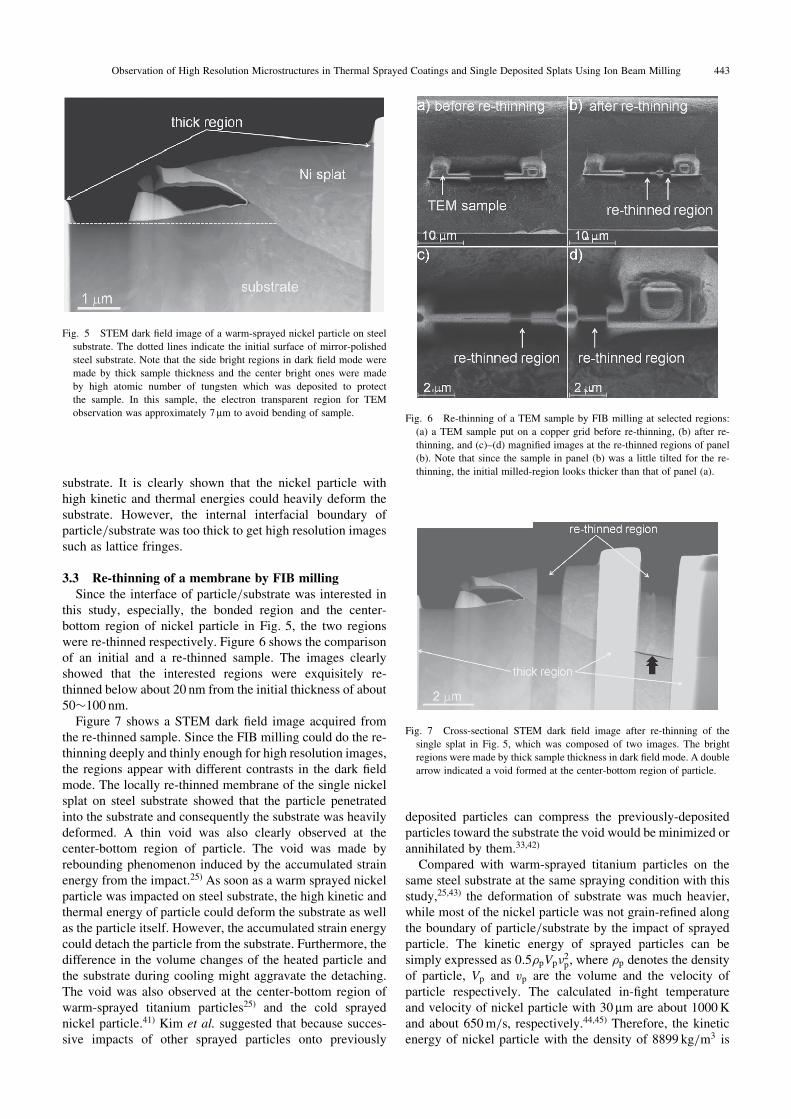
3.3 Re-thinning of a membrane by FIB millingSince the interface of particle/substrate was interested in
this study, especially, the bonded region and the center-bottom region of nickel particle in Fig. 5, the two regionswere re-thinned respectively. Figure 6 shows the comparisonof an initial and a re-thinned sample. The images clearlyshowed that the interested regions were exquisitely re-thinned below about 20 nm from the initial thickness of about50�100 nm.
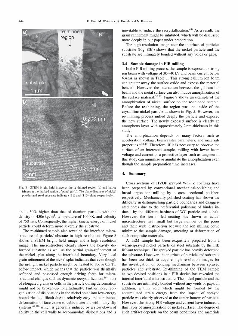
Figure 7 shows a STEM dark field image acquired fromthe re-thinned sample. Since the FIB milling could do the re-thinning deeply and thinly enough for high resolution images,the regions appear with different contrasts in the dark fieldmode. The locally re-thinned membrane of the single nickelsplat on steel substrate showed that the particle penetratedinto the substrate and consequently the substrate was heavilydeformed. A thin void was also clearly observed at thecenter-bottom region of particle. The void was made byrebounding phenomenon induced by the accumulated strainenergy from the impact.25) As soon as a warm sprayed nickelparticle was impacted on steel substrate, the high kinetic andthermal energy of particle could deform the substrate as wellas the particle itself. However, the accumulated strain energycould detach the particle from the substrate. Furthermore, thedifference in the volume changes of the heated particle andthe substrate during cooling might aggravate the detaching.The void was also observed at the center-bottom region ofwarm-sprayed titanium particles25) and the cold sprayednickel particle.41) Kim et al. suggested that because succes-sive impacts of other sprayed particles onto previously
deposited particles can compress the previously-depositedparticles toward the substrate the void would be minimized orannihilated by them.33,42)
Compared with warm-sprayed titanium particles on thesame steel substrate at the same spraying condition with thisstudy,25,43) the deformation of substrate was much heavier,while most of the nickel particle was not grain-refined alongthe boundary of particle/substrate by the impact of sprayedparticle. The kinetic energy of sprayed particles can besimply expressed as 0:5�pVp�
2p, where �p denotes the density
of particle, Vp and vp are the volume and the velocity ofparticle respectively. The calculated in-fight temperatureand velocity of nickel particle with 30 mm are about 1000Kand about 650m/s, respectively.44,45) Therefore, the kineticenergy of nickel particle with the density of 8899 kg/m3 is
Fig. 6 Re-thinning of a TEM sample by FIB milling at selected regions:
(a) a TEM sample put on a copper grid before re-thinning, (b) after re-
thinning, and (c)–(d) magnified images at the re-thinned regions of panel
(b). Note that since the sample in panel (b) was a little tilted for the re-
thinning, the initial milled-region looks thicker than that of panel (a).
Fig. 7 Cross-sectional STEM dark field image after re-thinning of the
single splat in Fig. 5, which was composed of two images. The bright
regions were made by thick sample thickness in dark field mode. A double
arrow indicated a void formed at the center-bottom region of particle.
Fig. 5 STEM dark field image of a warm-sprayed nickel particle on steel
substrate. The dotted lines indicate the initial surface of mirror-polished
steel substrate. Note that the side bright regions in dark field mode were
made by thick sample thickness and the center bright ones were made
by high atomic number of tungsten which was deposited to protect
the sample. In this sample, the electron transparent region for TEM
observation was approximately 7mm to avoid bending of sample.
Observation of High Resolution Microstructures in Thermal Sprayed Coatings and Single Deposited Splats Using Ion Beam Milling 443
about 50% higher than that of titanium particle with thedensity of 4506 kg/m3, temperature of 1040K, and velocityof 750m/s. Consequently, the higher kinetic energy of nickelparticle could deform more severely the substrate.
The re-thinned sample also revealed the interface micro-structure of particle/substrate in high resolution. Figure 8shows a STEM bright field image and a high resolutionimage. The microstructure clearly shows the heavily de-formed substrate as well as the partial grain-refinement ofthe nickel splat along the interfacial boundary. Very localgrain refinement of the nickel splat indicates that even thoughthe in-flight nickel particle might be heated to above 0.5 Tm
before impact, which means that the particle was thermallysoftened and possessed enough driving force for micro-structural changes such as dynamic recrystallization,46) mostof elongated grains or cells in the particle during deformationmight not be broken-up longitudinally. Furthermore, reor-ganization of dislocations in the nickel splat into low-energyboundaries is difficult due to relatively easy and continuousdeformation of face centered cubic materials with many slipsystems,47,48) which is generally induced by a slow-down ofability in the cell walls to accommodate dislocations and is
inevitable to induce the recrystallization.49) As a result, thegrain refinement might be inhibited, which will be discussedmore deeply in our paper under preparation.
The high resolution image near the interface of particle/substrate (Fig. 8(b)) shows that the nickel particle and thesubstrate are intimately bonded without any voids or gaps.
3.4 Sample damage in FIB millingIn the FIB milling process, the sample is exposed to strong
ion beam with voltage of 30�40 kV and beam current below6.4 nA as shown in Table 1. This strong gallium ion beamcan sputter away the surface oxide and expose the materialbeneath. However, the interaction between the gallium ionbeam and the metal surface can also induce amorphization ofthe surface material.50,51) Figure 9 shows an example of theamorphization of nickel surface on the re-thinned sample.Before the re-thinning, the region was the inside of thecrystalline nickel particle as shown in Fig. 5. However, there-thinning process milled deeply the particle and exposedthe new surface. The newly exposed surface is clearly anamorphous layer with approximately 2 nm thickness in thisstudy.
The amorphization depends on many factors such asacceleration voltage, beam raster parameters, and materialsproperties.9,42,43) Therefore, if it is necessary to observe thesurface of an interested sample, milling with lower beamvoltage and current or a protective layer such as tungsten inthis study can minimize or annihilate the amorphization eventhough the sample preparation time increases.
4. Summary
Cross sections of HVOF sprayed WC-Co coatings havebeen prepared by conventional mechanical-polishing andbroad argon ion milling by a cross sectional polisher,respectively. Mechanically polished coating has shown thedifficulty in distinguishing particle boundaries and exagger-ated pores due to the preferential polishing of binder in-duced by the different hardness of WC particle and cobalt.However, the ion milled coating has shown an actualmicrostructure with small but large number of the poresand their wide distribution because the ion milling couldminimize the sample damage, smearing or deformation ofsuch composite materials.
A TEM sample has been exquisitely prepared from awarm-sprayed nickel particle on steel substrate by the FIBlift-out technique. The sprayed particle has heavily deformedthe substrate. However, the interface of particle and substratehas been too thick to acquire high resolution images forthe investigation of bonding mechanism between sprayedparticles and substrate. Re-thinning of the TEM sampleat two desired positions in a FIB device has revealed theinternal interfacial microstructure. The nickel particle and thesubstrate are intimately bonded without any voids or gaps. Inaddition, a thin void which might be formed by theaccumulated strain energy from the impact of sprayedparticle was clearly observed at the center-bottom of particle.However, the strong FIB voltage and current have induced athin layer of amorphization of nickel surface. The degree ofsuch artifact depends on the beam conditions and materials
Fig. 8 STEM bright field image at the re-thinned region (a) and lattice
fringes at the marked region of panel (a)(b). The plane distances of nickel
powder and steel substrate indicate (111) and (110) plane respectively.
444 K. Kim, M. Watanabe, S. Kuroda and N. Kawano

properties. The re-thinning function of FIB is useful andpowerful to analyze the interface of sprayed particle andsubstrate, which is unattainable in conventional TEMpreparation using mechanical milling and thinning.
Finally, it is worth mentioning future applications of there-thinning technique using FIB. Until now, many research-ers have just used the FIB lift-out technique in order tomake a small splat sample or several samples at limitedlocation(s) such as only interface of coating/substrate orparticle/particle or surface area in a thick coating for TEMobservation. By the re-thinning technique, however, one canmake a wide and large re-thinned sample covering from thesurface to the interface in a thick coating.
Acknowledgements
This research was supported by Nanotechnology Networkprogram and World Premier International Research CenterInitiative on Materials Nanoarchitectonics, MEXT, Japan,and KAKENHI 19360335.
REFERENCES
1) K. H. Kim, M. Watanabe, S. Kuroda and N. Kawano: Proc. Int. Therm.
Spray Conf. & Expo. on Thermal Spray: Global Solutions for Future
Applications, CD-ROM, (Singapore, 03-05 May 2010).
2) H. Takahashi, A. Sato, M. Takakura, N. Mori, J. Boerder, W. Knoll and
J. Critchell: Microchim. Acta. 155 (2006) 295.
3) P. Sudraud, G. Benassayag and M. Bon: Microelectron. Eng. 6 (1987)
583.
4) M. Shibata: JEOL news 39 (2004) 28.
5) J. H. Orloff and L. W. Swanson: J. Vac. Sci. Technol. 12 (1975) 1209.
6) W. H. Escovitz, T. R. Fox and R. L. Seiti: Proc. Nat. Acad. Sci. 72
(1975) 1826.
7) J. Melngailis: J. Vac. Sci. Technol. B 5 (1987) 469.
8) M. H. F. Overwijk, F. C. van den Heuvei and C. W. T. Bulle-Lieuwma:
J. Vac. Sci. Technol. B 11 (1993) 2121.
9) J. Li: JOM 58 (2006) 27.
10) J. Orloff, L. W. Swanson and M. Utlaut: J. Vac. Sci. Technol. B 14
(1996) 3759.
11) Y. Wu, M. Qu, L. A. Giannuzzi, S. Sampath and A. Gouldstone: Mater.
Res. Soc. Symp. Proc. 983 (2007) 1.
12) M. Watanabe, A. Owada, S. Kuroda and Y. Gotoh: Surf. Coat. Technol.
201 (2006) 619.
13) H. Huang, K. Eguchi and T. Yoshida: J. Therm. Spray Technol. 15
(2006) 72.
14) P. C. King, S. H. Zahiri and M. Jahedi: Acta Mater. 56 (2008) 5617.
15) L. A. Giannuzzi and F. A. Stevie: Micron 30 (1999) 197.
16) B. I. Prenitzer, L. A. Giannuzzi, K. Newman, S. R. Brown, R. B.
Irwin, T. L. Shofner and F. A. Stevie: Metall. Mater. Trans. A 29 (1998)
2399.
17) E. A. Preblea, H. A. McLeana, S. M. Kiesela, P. Miragliaa, M.
Albrechtb and R. F. Davis: Ultramicroscopy 92 (2002) 265.
18) H. Lia, K. A. Khora and P. Cheang: Biomaterials 25 (2004) 3463.
19) D. Rafaja, T. Schucknecht, V. Klemm, A. Paul and H. Berek: Surf.
Coat. Technol. 203 (2009) 3206.
20) H. Koivuluoto, M. Honkanen and P. Vuoristo: Surf. Coat. Technol. 204
(2010) 2353.
21) W. J. Trompetter, M. Hyland, P. Munroe and A. Markwitz: J. Therm.
Spray Technol. 14 (2005) 524.
22) K. Balani, A. Agarwal, S. Seal and J. Karthikeyan: Scr. Mater. 53
(2005) 845.
23) L. Li, B. Kharas, H. Zhang and S. Sampath: Mater. Sci. Eng. A 456
(2007) 35.
24) S. Barradas, V. Guipont, R. Molins, M. Jeandin, M. Arrigoni, M.
Boustie, C. Bolis, L. Berthe andM. Ducos: J. Therm. Spray Technol. 16
(2007) 548.
25) K. H. Kim, M.Watanabe, K. Mitsuishi, K. Iakoubovskii and S. Kuroda:
J. Phys. D: Appl. Phys. 42 (2009) 065304 (5pp).
26) K. H. Kim, M. Watanabe, J. Kawakita and S. Kuroda: J. Therm. Spray
Technol. 18 (2009) 392.
27) Y. Xiong, K. Kang, G. Bae, S. Yoon and C. Lee: Appl. Phys. Lett. 92
(2008) 194101.
28) A. Agarwal, T. McKechnie and S. Seal: J. Therm. Spray Technol. 12
(2003) 350.
29) M. Fukumoto, M. Mashiko, M. Yamada and E. Yamaguchi: J. Therm.
Spray Technol. 19 (2010) 89.
30) S. Reyntjens and C. Kubel: J. Cryst. Growth 275 (2005) e1849.
31) P. Chivavibul, M. Watanabe, S. Kuroda, J. Kawakita, M. Komatsu, K.
Sato and J. Kitamura: J. Therm. Spray Technol. 17 (2008) 750.
32) T. Schmidt, H. Assadi, F. Gartner, H. Richter, T. Stolenhoff, H. Kreye
and T. Klassen: J. Therm. Spray Technol. 18 (2009) 794.
33) K. H. Kim, M. Watanabe and S. Kuroda: Surf. Coat. Technol. 204
(2010) 2175.
34) S. Kuroda, J. Kawakita, M. Watanabe and H. Katanoda: Sci. Technol.
Adv. Mater. 9 (2008) 033002.
35) K. H. Kim, M. Watanabe and S. Kuroda: J. Therm. Spray Technol. 18
(2009) 490.
36) P. Chivavibul, M. Watanabe, S. Kuroda and K. Shinoda: Surf. Coat.
Technol. 202 (2007) 509.
37) L. Pawlowski: The Science and Engineering of Thermal Spray
Coatings, Second Edition, (John Wiley & Sons, Chichester, 2008).
38) J. Kawakita, S. Kuroda, T. Fukushima, H. Katanoda, K. Matsuo and H.
Fukanuma: Surf. Coat. Technol. 201 (2006) 1250.
39) M. Watanabe, P. Chivavibul, S. Kuroda, J. Kawakita, J. Kitamura and
K. Sato: J. Jpn. Inst. Metals 71 (2007) 853–859.
40) P. Chivavibul, M. Watanabe, S. Kuroda and M. Komatsu: Surf. Coat.
Fig. 9 Surface amorphization of FIB milled sample: (a) STEM bright field image at the edge of re-thinned region of Fig. 8(a) and (b)
lattice image at the marked region of (a).
Observation of High Resolution Microstructures in Thermal Sprayed Coatings and Single Deposited Splats Using Ion Beam Milling 445

Technol. 202 (2008) 5127.
41) Y. Xiong, G. Bae, X. Xiong and C. Lee: J. Therm. Spray Technol. 19
(2010) 575.
42) K. H. Kim and S. Kuroda: Scr. Mater. 63 (2010) 215.
43) K. H. Kim, M. Watanabe and S. Kuroda: Scr. Mater. 60 (2009) 710.
44) H. Katanoda, T. Kiriaki, T. Tachibanaki, J. Kawakita, S. Kuroda and
M. Fukuhara: J. Therm. Spray Technol. 18 (2009) 401.
45) K. H. Kim, M. Watanabe, H. Katanoda and S. Kuroda: Collected
Abstracts of the 2010 Spring Meeting of JIM, (2010) p. 312.
46) K. H. Kim, M. Watanabe, J. Kawakita and S. Kuroda: Scr. Mater. 59
(2008) 768.
47) G. E. Dieter: Mechanical Metallurgy, (McGraw-Hill, New York,
1986).
48) R. E. Reed-Hill and R. Abbaschian: Physical Metallurgy Principles,
(PWS-Kent Pub., Boston, 1992).
49) M. A. Meyers, V. F. Nesterenko, J. C. LaSalvia and Q. Xue: Mater. Sci.
Eng. A 317 (2001) 204.
50) J. P. McCaffrey, M.W. Phaneuf and L. D. Madsen: Ultramicroscopy 87
(2001) 97.
51) D. Kiener, C. Motz, M. Rester, M. Jenko and G. Dehm: Mater. Sci.
Eng. A 459 (2007) 262.
446 K. Kim, M. Watanabe, S. Kuroda and N. Kawano
Related Documents