11215A–ATARM–04-Nov-13 Scope The Atmel ® SAMA5D3x series is a high-performance, power-efficient, embedded MPU based on the ARM ® Cortex ® -A5 core, offering the best balance between performance and power consumption. The External Bus Interface (EBI) in SAMA5D3 microcontrollers consists of a Static Memory Controller (HSMC), which can support memory devices such as SRAM, PSRAM, PROM, EPROM, EEPROM, LCD module, NOR Flash and NAND Flash. This application note discusses the HSMC support for NAND Flash devices and describes how to use the sample code to make customized application code. It focuses on support for MLC NAND Flash and introduces the PMECC (Programmable Multibit Error Correction Code) Controller. 1. Reference Documentation Type Reference Documentation Datasheet SAMA5D3 Series Datasheet Micron MT29F32G08CBAC Datasheet Micron MT29F2G08ABAEA Datasheet Application Note MLC NAND Flash Support in SAM9G15/G25/G35/X25/X35 Microcontrollers with PMECC Controller Other SAMA5D3-EK Design & Manufacturing Files Software Package SAMA5D3 Software Package Application Note NAND Flash Support in SAMA5D3 Microcontrollers ARM-based Embedded MPU

Welcome message from author
This document is posted to help you gain knowledge. Please leave a comment to let me know what you think about it! Share it to your friends and learn new things together.
Transcript
11215A–ATARM–04-Nov-13
Scope
The Atmel® SAMA5D3x series is a high-performance, power-efficient, embedded MPU based on the ARM® Cortex®-A5 core, offering the best balance between performance and power consumption.
The External Bus Interface (EBI) in SAMA5D3 microcontrollers consists of a Static Memory Controller (HSMC), which can support memory devices such as SRAM, PSRAM, PROM, EPROM, EEPROM, LCD module, NOR Flash and NAND Flash.
This application note discusses the HSMC support for NAND Flash devices and describes how to use the sample code to make customized application code. It focuses on support for MLC NAND Flash and introduces the PMECC (Programmable Multibit Error Correction Code) Controller.
1. Reference Documentation
Type Reference Documentation
Datasheet
SAMA5D3 Series Datasheet
Micron MT29F32G08CBAC Datasheet
Micron MT29F2G08ABAEA Datasheet
Application NoteMLC NAND Flash Support in SAM9G15/G25/G35/X25/X35 Microcontrollers with PMECC Controller
Other SAMA5D3-EK Design & Manufacturing Files
Software Package SAMA5D3 Software Package
Application Note
NAND Flash Support in SAMA5D3 Microcontrollers
ARM-based Embedded MPU
3NAND Flash Support in SAMA5D3 Microcontrollers [APPLICATION NOTE]11215A–ATARM–04-Nov-13
Table of Contents
Scope . . . . . . . . . . . . . . . . . . . . . . . . . . . . . . . . . . . . . . . . . . . . . . . . . . . . 1
1. Reference Documentation . . . . . . . . . . . . . . . . . . . . . . . . . . . . . . . . . 1
Table of Contents . . . . . . . . . . . . . . . . . . . . . . . . . . . . . . . . . . . . . . . . . . . 3
2. Device Overview . . . . . . . . . . . . . . . . . . . . . . . . . . . . . . . . . . . . . . . . 52.1 SAMA5D3 Static Memory Controller Overview. . . . . . . . . . . . . . . . . . . . . . . . . 5
2.2 NAND Flash Controller . . . . . . . . . . . . . . . . . . . . . . . . . . . . . . . . . . . . . . . . . . . 5
2.3 PMECC Controller . . . . . . . . . . . . . . . . . . . . . . . . . . . . . . . . . . . . . . . . . . . . . . 8
2.3.1 What is ECC? . . . . . . . . . . . . . . . . . . . . . . . . . . . . . . . . . . . . . . . . . . 8
2.3.2 BCH Algorithm . . . . . . . . . . . . . . . . . . . . . . . . . . . . . . . . . . . . . . . . . . 8
2.3.3 SAMA5D3 PMECC Overview . . . . . . . . . . . . . . . . . . . . . . . . . . . . . . 8
2.4 NAND Flash Device Overview . . . . . . . . . . . . . . . . . . . . . . . . . . . . . . . . . . . . 10
2.5 Multi-Level Cell and Single-Level Cell NAND Flash . . . . . . . . . . . . . . . . . . . . 10
2.6 Open NAND Flash Interface (ONFI) . . . . . . . . . . . . . . . . . . . . . . . . . . . . . . . . 10
3. SAMA5D3 MLC NAND Flash Support Example . . . . . . . . . . . . . . . 113.1 Hardware Connection . . . . . . . . . . . . . . . . . . . . . . . . . . . . . . . . . . . . . . . . . . . 11
3.2 Software Implementation . . . . . . . . . . . . . . . . . . . . . . . . . . . . . . . . . . . . . . . . 12
3.2.1 Code Structure Overview . . . . . . . . . . . . . . . . . . . . . . . . . . . . . . . . 12
3.2.2 Initialize the NAND Flash . . . . . . . . . . . . . . . . . . . . . . . . . . . . . . . . . 13
3.2.3 Raw Access . . . . . . . . . . . . . . . . . . . . . . . . . . . . . . . . . . . . . . . . . . . 15
3.2.4 Access the NAND Flash with PMECC . . . . . . . . . . . . . . . . . . . . . . . 15
3.2.5 NFC, NFC SRAM and HSMC DMA Enable . . . . . . . . . . . . . . . . . . . 16
4. Performance Comparison between NFC and HSMC . . . . . . . . . . . 174.1 SAMA5D3 Accesses NAND Flash through HSMC with DMA. . . . . . . . . . . . . 17
4.2 SAMA5D3 Accesses NAND Flash with NFC plus SRAM . . . . . . . . . . . . . . . . 18
4.3 Performance Test Results . . . . . . . . . . . . . . . . . . . . . . . . . . . . . . . . . . . . . . . 18
5. Conclusion . . . . . . . . . . . . . . . . . . . . . . . . . . . . . . . . . . . . . . . . . . . . 19
Revision History . . . . . . . . . . . . . . . . . . . . . . . . . . . . . . . . . . . . . . . . . . . 20
1. Device Overview
1.1 SAMA5D3 Static Memory Controller Overview
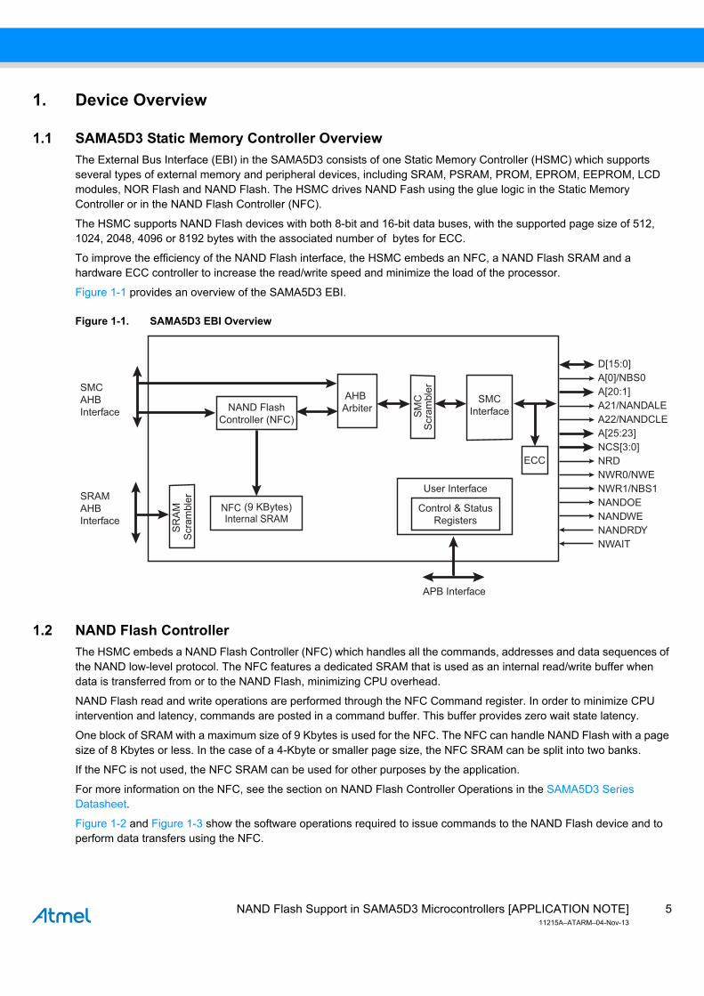
The External Bus Interface (EBI) in the SAMA5D3 consists of one Static Memory Controller (HSMC) which supports several types of external memory and peripheral devices, including SRAM, PSRAM, PROM, EPROM, EEPROM, LCD modules, NOR Flash and NAND Flash. The HSMC drives NAND Fash using the glue logic in the Static Memory Controller or in the NAND Flash Controller (NFC).
The HSMC supports NAND Flash devices with both 8-bit and 16-bit data buses, with the supported page size of 512, 1024, 2048, 4096 or 8192 bytes with the associated number of bytes for ECC.
To improve the efficiency of the NAND Flash interface, the HSMC embeds an NFC, a NAND Flash SRAM and a hardware ECC controller to increase the read/write speed and minimize the load of the processor.
Figure 1-1 provides an overview of the SAMA5D3 EBI.
Figure 1-1. SAMA5D3 EBI Overview
1.2 NAND Flash Controller
The HSMC embeds a NAND Flash Controller (NFC) which handles all the commands, addresses and data sequences of the NAND low-level protocol. The NFC features a dedicated SRAM that is used as an internal read/write buffer when data is transferred from or to the NAND Flash, minimizing CPU overhead.
NAND Flash read and write operations are performed through the NFC Command register. In order to minimize CPU intervention and latency, commands are posted in a command buffer. This buffer provides zero wait state latency.
One block of SRAM with a maximum size of 9 Kbytes is used for the NFC. The NFC can handle NAND Flash with a page size of 8 Kbytes or less. In the case of a 4-Kbyte or smaller page size, the NFC SRAM can be split into two banks.
If the NFC is not used, the NFC SRAM can be used for other purposes by the application.
For more information on the NFC, see the section on NAND Flash Controller Operations in the SAMA5D3 Series Datasheet.
Figure 1-2 and Figure 1-3 show the software operations required to issue commands to the NAND Flash device and to perform data transfers using the NFC.
SMC
Interface
NANDRDY
D[15:0]
NFCInternal SRAM
NAND Flash
Controller (NFC)
ECC
NWR0/NWE
NCS[3:0]
NWAIT
NANDOE
NANDWE
NRD
A[0]/NBS0
A[20:1]
NWR1/NBS1
A21/NANDALE
A22/NANDCLE
Control & Status
Registers
SRAM
AHB
Interface
AHB
Arbiter
Scra
mble
rS
MC
SMC
AHB
Interface
(9 KBytes)
User Interface
A[25:23]
APB Interface
Scra
mble
rS
RA
M
5NAND Flash Support in SAMA5D3 Microcontrollers [APPLICATION NOTE]11215A–ATARM–04-Nov-13
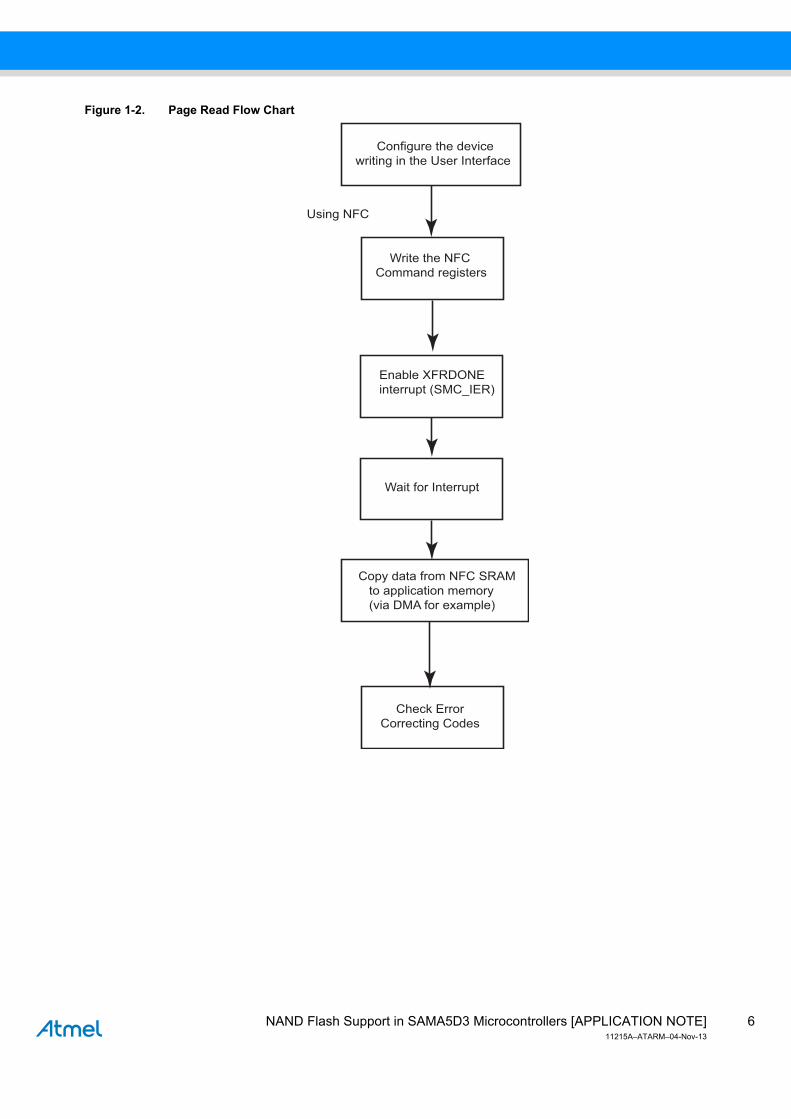
Figure 1-2. Page Read Flow Chart
Configure the device
writing in the User Interface
Write the NFC
Command registers
Enable XFRDONE
interrupt (SMC_IER)
Wait for Interrupt
Copy data from NFC SRAM
to application memory
(via DMA for example)
Using NFC
Check Error
Correcting Codes
6NAND Flash Support in SAMA5D3 Microcontrollers [APPLICATION NOTE]11215A–ATARM–04-Nov-13

Figure 1-3. Page Program Flow Chart
Configure the device writing in the User interface
Write data in the NFC SRAM (CPU or DMA) Enable XFRDONE
Write the CommandRegister through the AHB interface
Write ECC
Wait for interrupt
Wait for Ready/Busy interrupt
7NAND Flash Support in SAMA5D3 Microcontrollers [APPLICATION NOTE]11215A–ATARM–04-Nov-13
1.3 PMECC Controller
1.3.1 What is ECC?
Because of limitations in Flash technology, NAND devices are subject to data failures that occur during device operation. To ensure data read/write integrity, system error-checking and correction (ECC) algorithms must be implemented. Some NAND Flash devices feature an embedded ECC controller which can be enabled and disabled. Most ARM processors also feature hardware ECC controllers. The embedded ECC controller and the related decoding software are capable of generating redundancy for the correction of single or multiple bits of data.
1.3.2 BCH Algorithm
Binary BCH (Bose, Chaudhuri, Hocquenghem) codes were first discovered by A. Hocquenghem in 1959 and independently by R.C. Bose and D.K. Ray-Chaudhuri in 1960. BCH codes are a family of cyclic codes, with an algebraic structure which is useful to simplify the encoding and decoding procedures. Binary BCH codes with minimum distance 3 are better known as Hamming codes. BCH codes are a generalization of Hamming codes for multiple error correction, which have been a very popular choice in memory devices, because of their simple and fast encoding and decoding procedures.
1.3.3 SAMA5D3 PMECC Overview
The PMECC (Programmable Multibit Error Correction Code) Controller embedded in SAMA5D3 devices is a programmable binary BCH encoder/decoder. This controller can be used to generate redundancy information for both SLC and MLC NAND devices. It supports redundancy for correction of 2, 4, 8, 12 or 24 errors per sector of data. The sector size is programmable and can be set to 512 or 1024 bytes. The PMECC module generates redundancy at encoding time, when a NAND write page operation is performed. The redundancy is appended to the page and written in the spare area. This operation is performed by the processor. It moves the content of the PMECCx register into the NAND Flash memory. The number of registers depends on the selected error correction capability. This operation is executed for each sector. At decoding time, the PMECC module generates the remainders of the received codeword by the minimal polynomials. When all remainders for a given sector are set to zero, no error occurred. When the remainders are different from zero, the codeword is corrupted and further processing is required.
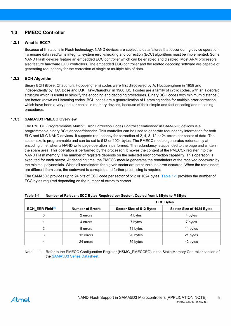
The SAMA5D3 provides up to 24 bits of ECC code per sector of 512 or 1024 bytes. Table 1-1 provides the number of ECC bytes required depending on the number of errors to correct.
Note: 1. Refer to the PMECC Configuration Register (HSMC_PMECCFG) in the Static Memory Controller section of the SAMA5D3 Series Datasheet.
Table 1-1. Number of Relevant ECC Bytes Required per Sector , Copied from LSByte to MSByte
BCH_ERR Field(1) Number of Errors
ECC Bytes
Sector Size of 512 Bytes Sector Size of 1024 Bytes
0 2 errors 4 bytes 4 bytes
1 4 errors 7 bytes 7 bytes
2 8 errors 13 bytes 14 bytes
3 12 errors 20 bytes 21 bytes
4 24 errors 39 bytes 42 bytes
8NAND Flash Support in SAMA5D3 Microcontrollers [APPLICATION NOTE]11215A–ATARM–04-Nov-13
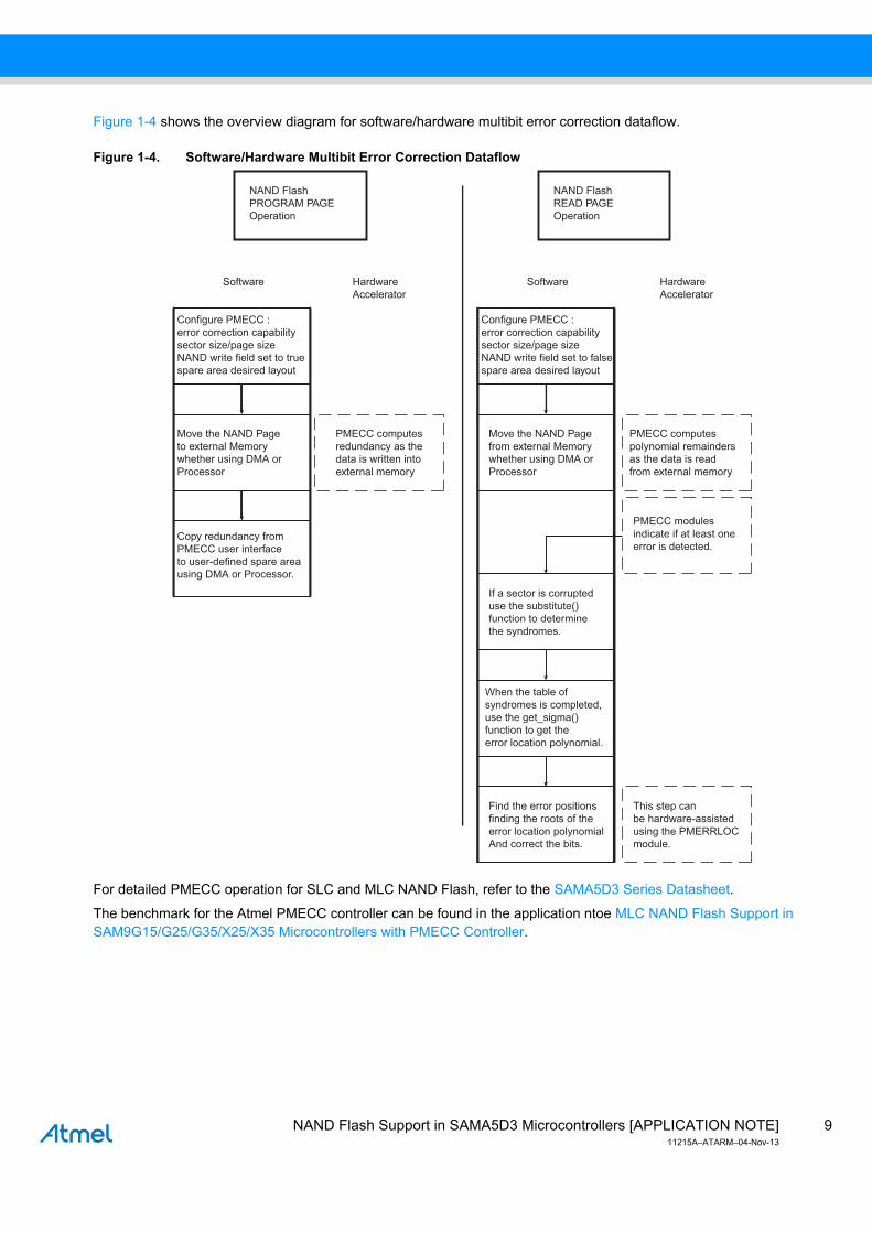
Figure 1-4 shows the overview diagram for software/hardware multibit error correction dataflow.
Figure 1-4. Software/Hardware Multibit Error Correction Dataflow
For detailed PMECC operation for SLC and MLC NAND Flash, refer to the SAMA5D3 Series Datasheet.
The benchmark for the Atmel PMECC controller can be found in the application ntoe MLC NAND Flash Support in SAM9G15/G25/G35/X25/X35 Microcontrollers with PMECC Controller.
ATMEL CONFID
ENTIAL
ATMEL CONFID
ENTIAL
NAND Flash
PROGRAM PAGE
Operation
Configure PMECC :
error correction capability
sector size/page size
NAND write field set to true
spare area desired layout
Move the NAND Page
to external Memory
whether using DMA or
Processor
Copy redundancy from
PMECC user interface
to user-defined spare area
using DMA or Processor.
PMECC computes
redundancy as the
data is written into
external memory
NAND Flash
READ PAGE
Operation
Configure PMECC :
error correction capability
sector size/page size
NAND write field set to false
spare area desired layout
Move the NAND Page
from external Memory
whether using DMA or
Processor
PMECC computes
polynomial remainders
as the data is read
from external memory
PMECC modules
indicate if at least one
error is detected.
If a sector is corrupted
use the substitute()
function to determine
the syndromes.
When the table of
syndromes is completed,
use the get_sigma()
function to get the
error location polynomial.
Find the error positions
finding the roots of the
error location polynomial
And correct the bits.
This step can
be hardware-assisted
using the PMERRLOC
module.
Hardware
Accelerator
Software Hardware
Accelerator
Software
9NAND Flash Support in SAMA5D3 Microcontrollers [APPLICATION NOTE]11215A–ATARM–04-Nov-13
1.4 NAND Flash Device Overview
The NAND Flash array is organized as a series of blocks divided into several pages.
Data is stored either in byte (8 bits) or half-word (16 bits) format depending on the device type.
Each page consists of a main area for storing data and a spare area (physically similar) typically used for data error identification and correction, wear levelling, etc.
One particularity of NAND Flash devices is that they may contain a percentage of invalid blocks in the memory array. The NAND Flash manufacturer identifies and marks the bad blocks as "Invalid blocks". This information is stored in the block spare area (1st or 2nd page of the block).
The existence of bad blocks does not affect the other blocks because each block is independent and individually isolated from the bit lines by block select transistors. As NAND Flash devices have a finite lifetime (approximately 60 K~100 K SLC / 3 K~5 K MLC), additional invalid blocks may develop while being used. Storing data requires bad-block management and data error identification and correction.
1.5 Multi-Level Cell and Single-Level Cell NAND Flash
The two most common types of NAND Flash technology are single-level cell (SLC) and multi- level cell (MLC).
In SLC NAND Flash, each cell exists in one of two states, storing one bit of information per cell. This technology is used in the majority of high-performance media card and wireless processor applications.
MLC NAND Flash was developed more recently to achieve a higher bit density, creating a Flash chip with a greater memory capacity for a given die size.
MLC NAND Flash uses multiple levels per cell to allow more bits to be stored using the same number of transistors. Most MLC NAND Flash has four possible states per cell, thus it can store two bits of information per cell. The primary benefit of MLC Flash is its lower cost per unit of storage due to the higher data density. However, since MLC technology reduces the amount of margin separating the states, there is a greater risk of errors. The higher error rate of MLC NAND results in lower write speed, a smaller number of program-erase cycles and in higher power consumption compared to SLC Flash memory.Compared to SLC, MLC architecture requires more ECC bits to compensate for the resulting higher error rate. Thus the algorithm and the related software are more complex. To reduce software complexity, the SAMA5D3 features a built-in PMECC module that supports MLC ECC requirement.
1.6 Open NAND Flash Interface (ONFI)
The Open NAND Flash Interface (ONFI) Working Group is a consortium of technology companies working to develop open standards for NAND Flash memory chips and devices that communicate with them. The formation of ONFI was announced at the Intel Developer Forum in March 2006.
ONFI defines a standardized NAND Flash device interface, which provides the means for a system to seamlessly make use of new NAND devices that may not have existed at the time the system was designed, reduces development cost/complexity and improves time to market.
The NAND Flash library provides a procedure to check if the NAND Flash is ONFI-compliant by sending a Read ID command (0x90) with 0x20 as the address parameter. If the NAND Flash is ONFI-compliant, it will retrieve the ONFI parameters using the PMECC configuration from the page block. The ONFI 2.0 page block includes the following information:
Table 1-2. ONFI 2.0 Page Block Information
Revision Information and Features
Manufacture Information
Memory Organization
Electrical Parameters
Vendor
10NAND Flash Support in SAMA5D3 Microcontrollers [APPLICATION NOTE]11215A–ATARM–04-Nov-13
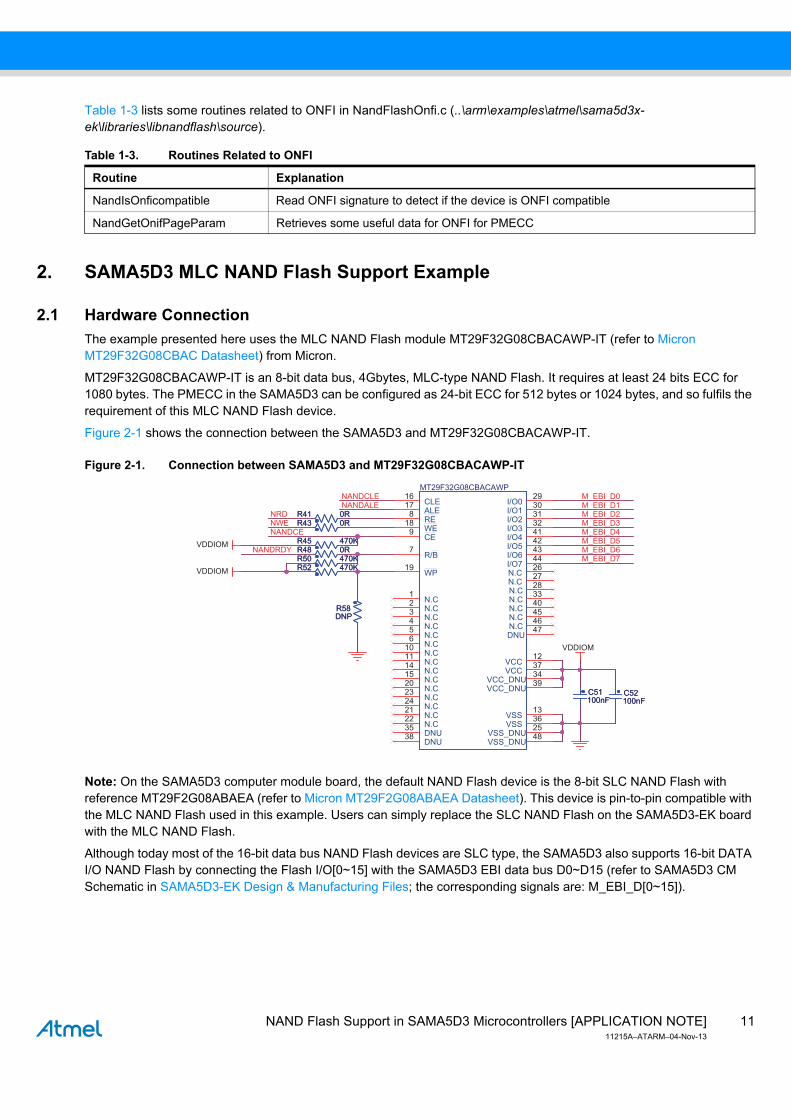
Table 1-3 lists some routines related to ONFI in NandFlashOnfi.c (..\arm\examples\atmel\sama5d3x-ek\libraries\libnandflash\source).
2. SAMA5D3 MLC NAND Flash Support Example
2.1 Hardware Connection
The example presented here uses the MLC NAND Flash module MT29F32G08CBACAWP-IT (refer to Micron MT29F32G08CBAC Datasheet) from Micron.
MT29F32G08CBACAWP-IT is an 8-bit data bus, 4Gbytes, MLC-type NAND Flash. It requires at least 24 bits ECC for 1080 bytes. The PMECC in the SAMA5D3 can be configured as 24-bit ECC for 512 bytes or 1024 bytes, and so fulfils the requirement of this MLC NAND Flash device.
Figure 2-1 shows the connection between the SAMA5D3 and MT29F32G08CBACAWP-IT.
Figure 2-1. Connection between SAMA5D3 and MT29F32G08CBACAWP-IT
Note: On the SAMA5D3 computer module board, the default NAND Flash device is the 8-bit SLC NAND Flash with reference MT29F2G08ABAEA (refer to Micron MT29F2G08ABAEA Datasheet). This device is pin-to-pin compatible with the MLC NAND Flash used in this example. Users can simply replace the SLC NAND Flash on the SAMA5D3-EK board with the MLC NAND Flash.
Although today most of the 16-bit data bus NAND Flash devices are SLC type, the SAMA5D3 also supports 16-bit DATA I/O NAND Flash by connecting the Flash I/O[0~15] with the SAMA5D3 EBI data bus D0~D15 (refer to SAMA5D3 CM Schematic in SAMA5D3-EK Design & Manufacturing Files; the corresponding signals are: M_EBI_D[0~15]).
Table 1-3. Routines Related to ONFI
Routine Explanation
NandIsOnficompatible Read ONFI signature to detect if the device is ONFI compatible
NandGetOnifPageParam Retrieves some useful data for ONFI for PMECC
NRDNWENANDCE
M_EBI_D2
M_EBI_D4M_EBI_D3
M_EBI_D6M_EBI_D7
M_EBI_D5
M_EBI_D0M_EBI_D1
NANDCLENANDALE
NANDRDYVDDIOM
VDDIOM
VDDIOM
R48 0RR48 0R
C51100nFC51100nF
C52100nFC52100nF
R50 470KR50 470K
MT29F32G08CBACAWP
WE18
N.C6
VCC37
CE9
RE8
N.C20
WP19
N.C5
N.C1
N.C2
N.C3
N.C4
N.C22
DNU35
N.C23
N.C24
R/B7
N.C26
N.C27
N.C28
I/O029
VCC_DNU34
N.C21
VSS36
DNU38
VCC_DNU39
VCC12
VSS13
ALE17
N.C11 N.C10
N.C14
N.C15
CLE16
VSS_DNU25
N.C33
I/O130
I/O332I/O231
DNU47N.C46N.C45
I/O744I/O643I/O542I/O441
N.C40
VSS_DNU48
R41 0RR41 0R
R58DNPR58DNP
R52 470KR52 470K
R45 470KR45 470K
R43 0RR43 0R
11NAND Flash Support in SAMA5D3 Microcontrollers [APPLICATION NOTE]11215A–ATARM–04-Nov-13
2.2 Software Implementation
Atmel provides a software package for the SAMA5D3 that is compatible with CodeSourcery and IAR environments. In this application note, the example shown is in the IAR environment.
To begin, download and install the most recent version of the SAMA5D3 Software Package. The library for SAMA5D3 is installed in the default directory Program Files\IAR Systems\Embedded Workbench 6.0xxx\arm\examples\Atmel\sama5d3x-ek.
Note: The IAR version number in the directory name may be different depending on the version of IAR installed on the user’s computer.
2.2.1 Code Structure Overview
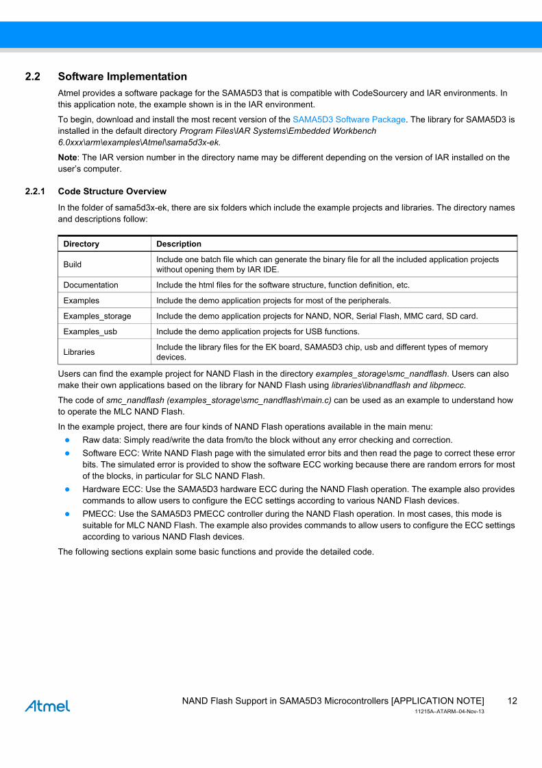
In the folder of sama5d3x-ek, there are six folders which include the example projects and libraries. The directory names and descriptions follow:
Users can find the example project for NAND Flash in the directory examples_storage\smc_nandflash. Users can also make their own applications based on the library for NAND Flash using libraries\libnandflash and libpmecc.
The code of smc_nandflash (examples_storage\smc_nandflash\main.c) can be used as an example to understand how to operate the MLC NAND Flash.
In the example project, there are four kinds of NAND Flash operations available in the main menu:
Raw data: Simply read/write the data from/to the block without any error checking and correction.
Software ECC: Write NAND Flash page with the simulated error bits and then read the page to correct these error bits. The simulated error is provided to show the software ECC working because there are random errors for most of the blocks, in particular for SLC NAND Flash.
Hardware ECC: Use the SAMA5D3 hardware ECC during the NAND Flash operation. The example also provides commands to allow users to configure the ECC settings according to various NAND Flash devices.
PMECC: Use the SAMA5D3 PMECC controller during the NAND Flash operation. In most cases, this mode is suitable for MLC NAND Flash. The example also provides commands to allow users to configure the ECC settings according to various NAND Flash devices.
The following sections explain some basic functions and provide the detailed code.
Directory Description
BuildInclude one batch file which can generate the binary file for all the included application projects without opening them by IAR IDE.
Documentation Include the html files for the software structure, function definition, etc.
Examples Include the demo application projects for most of the peripherals.
Examples_storage Include the demo application projects for NAND, NOR, Serial Flash, MMC card, SD card.
Examples_usb Include the demo application projects for USB functions.
LibrariesInclude the library files for the EK board, SAMA5D3 chip, usb and different types of memory devices.
12NAND Flash Support in SAMA5D3 Microcontrollers [APPLICATION NOTE]11215A–ATARM–04-Nov-13
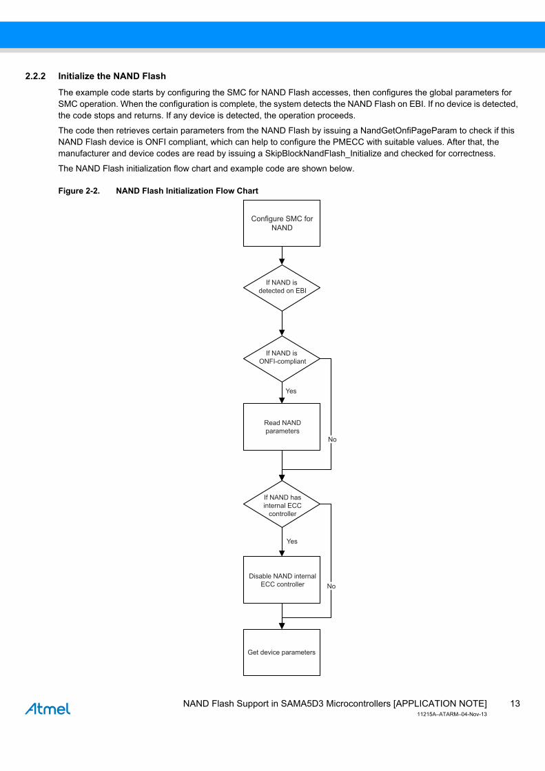
2.2.2 Initialize the NAND Flash
The example code starts by configuring the SMC for NAND Flash accesses, then configures the global parameters for SMC operation. When the configuration is complete, the system detects the NAND Flash on EBI. If no device is detected, the code stops and returns. If any device is detected, the operation proceeds.
The code then retrieves certain parameters from the NAND Flash by issuing a NandGetOnfiPageParam to check if this NAND Flash device is ONFI compliant, which can help to configure the PMECC with suitable values. After that, the manufacturer and device codes are read by issuing a SkipBlockNandFlash_Initialize and checked for correctness.
The NAND Flash initialization flow chart and example code are shown below.
Figure 2-2. NAND Flash Initialization Flow Chart
Configure SMC for
NAND
If NAND is
detected on EBI
If NAND is
ONFI-compliant
Read NAND
parameters
If NAND has
internal ECC
controller
Disable NAND internal
ECC controller
Get device parameters
Yes
Yes
No
No
13NAND Flash Support in SAMA5D3 Microcontrollers [APPLICATION NOTE]11215A–ATARM–04-Nov-13
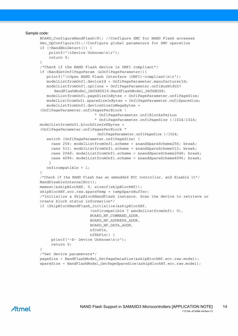
Sample code:BOARD_ConfigureNandFlash(8); //Configure SMC for NAND Flash accessesSmc_OpConfigure(0);//Configure global parameters for SMC operationif (!NandEbiDetect()) { printf("\tDevice Unknown\n\r"); return 0;}/*Check if the NAND Flash device is ONFI compliant*/if (NandGetOnfiPageParam (&OnfiPageParameter)){ printf("\tOpen NAND Flash Interface (ONFI)-compliant\n\r"); modelListfromOnfi.deviceId = OnfiPageParameter.manufacturerId; modelListfromOnfi.options = OnfiPageParameter.onfiBusWidth?
NandFlashModel_DATABUS16:NandFlashModel_DATABUS8; modelListfromOnfi.pageSizeInBytes = OnfiPageParameter.onfiPageSize; modelListfromOnfi.spareSizeInBytes = OnfiPageParameter.onfiSpareSize; modelListfromOnfi.deviceSizeInMegaBytes = (OnfiPageParameter.onfiPagesPerBlock \ * OnfiPageParameter.onfiBlocksPerLun * OnfiPageParameter.onfiPageSize )/1024/1024;modelListfromOnfi.blockSizeInKBytes = (OnfiPageParameter.onfiPagesPerBlock *
OnfiPageParameter.onfiPageSize )/1024; switch (OnfiPageParameter.onfiPageSize) { case 256: modelListfromOnfi.scheme = &nandSpareScheme256; break; case 512: modelListfromOnfi.scheme = &nandSpareScheme512; break; case 2048: modelListfromOnfi.scheme = &nandSpareScheme2048; break; case 4096: modelListfromOnfi.scheme = &nandSpareScheme4096; break; } onficompatible = 1;} /*Check if the NAND Flash has an embedded ECC controller, and disable it*/NandDisableInternalEcc();memset(&skipBlockNf, 0, sizeof(skipBlockNf));skipBlockNf.ecc.raw.spareTemp = tempSpareBuffer;/*Initialize a SkipBlockNandFlash instance. Scan the device to retrieve or create block status information*/if (SkipBlockNandFlash_Initialize(&skipBlockNf, (onficompatible ? &modelListfromOnfi: 0), BOARD_NF_COMMAND_ADDR, BOARD_NF_ADDRESS_ADDR, BOARD_NF_DATA_ADDR, nfCePin, nfRbPin)) { printf("-E- Device Unknown\n\r"); return 0;}/*Get device parameters*/pageSize = NandFlashModel_GetPageDataSize(&skipBlockNf.ecc.raw.model);spareSize = NandFlashModel_GetPageSpareSize(&skipBlockNf.ecc.raw.model);
14NAND Flash Support in SAMA5D3 Microcontrollers [APPLICATION NOTE]11215A–ATARM–04-Nov-13
2.2.3 Raw Access
Raw access means reading or writing the block without any ECC. In the demo, raw access includes the following operations:
Erasing the block before write and read
Writinge a page of data to the given block
Reading the page
Measuring the write and read performance in sample code by calculating the write or read time
The sample code for accessing the NAND in _pageAccess() function:/*Erase block*/SkipBlockNandFlash_EraseBlock(&skipBlockNf, block, SCRUB_ERASE);/*Write the page*/for ( i = 0; i < numPagesPerBlock; i++) SkipBlockNandFlash_WritePage(&skipBlockNf, block, i, pageBuffer, 0);/*Read the page*/for ( i = 0; i < numPagesPerBlock; i++) SkipBlockNandFlash_ReadPage(&skipBlockNf, block, i, pageBuffer, 0);
The detailed definitions of SkipBlockNandFlash_WritePage () and SkipBlockNandFlash_ReadPage() are in SkipBlockNandFlash.c file under libraries\libnandflash\source directory.
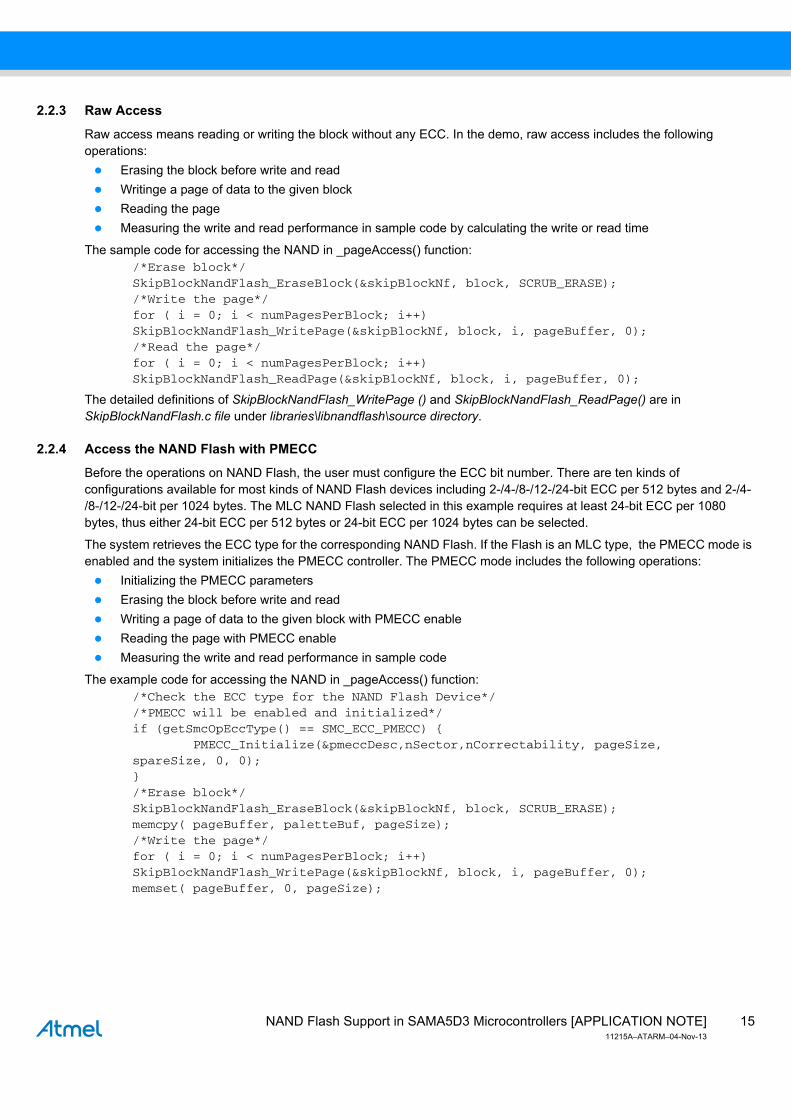
2.2.4 Access the NAND Flash with PMECC
Before the operations on NAND Flash, the user must configure the ECC bit number. There are ten kinds of configurations available for most kinds of NAND Flash devices including 2-/4-/8-/12-/24-bit ECC per 512 bytes and 2-/4-/8-/12-/24-bit per 1024 bytes. The MLC NAND Flash selected in this example requires at least 24-bit ECC per 1080 bytes, thus either 24-bit ECC per 512 bytes or 24-bit ECC per 1024 bytes can be selected.
The system retrieves the ECC type for the corresponding NAND Flash. If the Flash is an MLC type, the PMECC mode is enabled and the system initializes the PMECC controller. The PMECC mode includes the following operations:
Initializing the PMECC parameters
Erasing the block before write and read
Writing a page of data to the given block with PMECC enable
Reading the page with PMECC enable
Measuring the write and read performance in sample code
The example code for accessing the NAND in _pageAccess() function:/*Check the ECC type for the NAND Flash Device*//*PMECC will be enabled and initialized*/if (getSmcOpEccType() == SMC_ECC_PMECC) { PMECC_Initialize(&pmeccDesc,nSector,nCorrectability, pageSize, spareSize, 0, 0);}/*Erase block*/SkipBlockNandFlash_EraseBlock(&skipBlockNf, block, SCRUB_ERASE);memcpy( pageBuffer, paletteBuf, pageSize);/*Write the page*/for ( i = 0; i < numPagesPerBlock; i++) SkipBlockNandFlash_WritePage(&skipBlockNf, block, i, pageBuffer, 0);memset( pageBuffer, 0, pageSize);
15NAND Flash Support in SAMA5D3 Microcontrollers [APPLICATION NOTE]11215A–ATARM–04-Nov-13
/*Read the page*/for ( i = 0; i < numPagesPerBlock; i++) SkipBlockNandFlash_ReadPage(&skipBlockNf, block, i, pageBuffer, 0);
For the details on how to initialize the PMECC peripheral, refer to the function definition of PMECC_Initialize() in pmecc.c file under libaries\libpmecc\source directory.
2.2.5 NFC, NFC SRAM and HSMC DMA Enable
The SAMA5D3 EBI consists of a Static Memory Controller (HSMC), with the HSMC embedding an NFC (NAND Flash Controller). The NFC has SRAM which can be used as internal read/write buffer for the NAND data transfer. In HSMC mode, the DMA is used and data is transferred without processor intervention.
Both HSMC and NFC modes have benefits. In HSMC mode, the user has more flexibility to adjust the NAND operation timing depending on the parameters of the corresponding NAND Flash to achieve the fastest read/write speed. In NFC mode, after configuring the NFC parameters, data transfer can be performed automatically without processor intervention, which helps to improve the NAND Flash operation speed and save processor bandwidth. Users can select either mode depending on application requirements.
In the example code, there are options for users to configure the NAND Flash operation by enabling or disabling NFC, NFC SRAM and HSMC DMA.
Users can check the configuration by getting the return value of the following functions:isSMCOpNfcEn(); //If return 0, NFC is disabled; if return 1, NFC is enabledisSMCopNfcSramEn(); //If return 0, NFC SRAM is disabled; if return 1, NFC SRAM is enabledisSMCOpTransDmaen(); //If return 0, DMA mode is disabled; if return 1, DMA mode is enabledvoid enableSmcOpNfc(void) //Briefly set the SMC NAND global parameter to enable the NFCvoid enableSmcOpNfcSram(void) //Briefly set the SMC NAND global parameter to enable the NFC Host SRAMvoid enableSmcOpTransDma(void) //Briefly set the SMC NAND global parameter to enable the DMA data transfervoid Smc_Issue_Cle_Ale(const struct RawNandFlash *raw,uint8_t mode, uint32_t cmd1,uint32_t cmd2,uint32_t colAddress,uint32_t rowAddress)//Configure the NFC parameters
For the detailed functions on how to operate the NAND Flash with HSMC or NFC mode, please refer to the NandSmc.c file under libraries\libnandflash\source directory.
16NAND Flash Support in SAMA5D3 Microcontrollers [APPLICATION NOTE]11215A–ATARM–04-Nov-13
3. Performance Comparison between NFC and HSMC
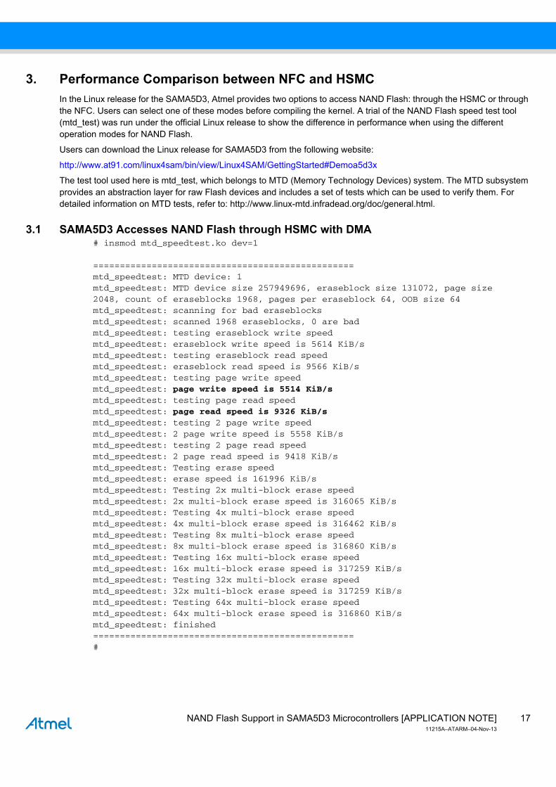
In the Linux release for the SAMA5D3, Atmel provides two options to access NAND Flash: through the HSMC or through the NFC. Users can select one of these modes before compiling the kernel. A trial of the NAND Flash speed test tool (mtd_test) was run under the official Linux release to show the difference in performance when using the different operation modes for NAND Flash.
Users can download the Linux release for SAMA5D3 from the following website:
http://www.at91.com/linux4sam/bin/view/Linux4SAM/GettingStarted#Demoa5d3x
The test tool used here is mtd_test, which belongs to MTD (Memory Technology Devices) system. The MTD subsystem provides an abstraction layer for raw Flash devices and includes a set of tests which can be used to verify them. For detailed information on MTD tests, refer to: http://www.linux-mtd.infradead.org/doc/general.html.
3.1 SAMA5D3 Accesses NAND Flash through HSMC with DMA# insmod mtd_speedtest.ko dev=1
=================================================mtd_speedtest: MTD device: 1mtd_speedtest: MTD device size 257949696, eraseblock size 131072, page size 2048, count of eraseblocks 1968, pages per eraseblock 64, OOB size 64mtd_speedtest: scanning for bad eraseblocksmtd_speedtest: scanned 1968 eraseblocks, 0 are badmtd_speedtest: testing eraseblock write speedmtd_speedtest: eraseblock write speed is 5614 KiB/smtd_speedtest: testing eraseblock read speedmtd_speedtest: eraseblock read speed is 9566 KiB/smtd_speedtest: testing page write speedmtd_speedtest: page write speed is 5514 KiB/smtd_speedtest: testing page read speedmtd_speedtest: page read speed is 9326 KiB/smtd_speedtest: testing 2 page write speedmtd_speedtest: 2 page write speed is 5558 KiB/smtd_speedtest: testing 2 page read speedmtd_speedtest: 2 page read speed is 9418 KiB/smtd_speedtest: Testing erase speedmtd_speedtest: erase speed is 161996 KiB/smtd_speedtest: Testing 2x multi-block erase speedmtd_speedtest: 2x multi-block erase speed is 316065 KiB/smtd_speedtest: Testing 4x multi-block erase speedmtd_speedtest: 4x multi-block erase speed is 316462 KiB/smtd_speedtest: Testing 8x multi-block erase speedmtd_speedtest: 8x multi-block erase speed is 316860 KiB/smtd_speedtest: Testing 16x multi-block erase speedmtd_speedtest: 16x multi-block erase speed is 317259 KiB/smtd_speedtest: Testing 32x multi-block erase speedmtd_speedtest: 32x multi-block erase speed is 317259 KiB/smtd_speedtest: Testing 64x multi-block erase speedmtd_speedtest: 64x multi-block erase speed is 316860 KiB/smtd_speedtest: finished=================================================#
17NAND Flash Support in SAMA5D3 Microcontrollers [APPLICATION NOTE]11215A–ATARM–04-Nov-13

3.2 SAMA5D3 Accesses NAND Flash with NFC plus SRAM# insmod mtd_speedtest.ko dev=1
=================================================mtd_speedtest: MTD device: 1mtd_speedtest: MTD device size 257949696, eraseblock size 131072, page size 2048, count of eraseblocks 1968, pages per eraseblock 64, OOB size 64mtd_speedtest: scanning for bad eraseblocksmtd_speedtest: scanned 1968 eraseblocks, 0 are badmtd_speedtest: testing eraseblock write speedmtd_speedtest: eraseblock write speed is 5631 KiB/smtd_speedtest: testing eraseblock read speedmtd_speedtest: eraseblock read speed is 11504 KiB/smtd_speedtest: testing page write speedmtd_speedtest: page write speed is 5436 KiB/smtd_speedtest: testing page read speedmtd_speedtest: page read speed is 11249 KiB/smtd_speedtest: testing 2 page write speedmtd_speedtest: 2 page write speed is 5528 KiB/smtd_speedtest: testing 2 page read speedmtd_speedtest: 2 page read speed is 11371 KiB/smtd_speedtest: Testing erase speedmtd_speedtest: erase speed is 155208 KiB/smtd_speedtest: Testing 2x multi-block erase speedmtd_speedtest: 2x multi-block erase speed is 296009 KiB/smtd_speedtest: Testing 4x multi-block erase speedmtd_speedtest: 4x multi-block erase speed is 298111 KiB/smtd_speedtest: Testing 8x multi-block erase speedmtd_speedtest: 8x multi-block erase speed is 299885 KiB/smtd_speedtest: Testing 16x multi-block erase speedmtd_speedtest: 16x multi-block erase speed is 300243 KiB/smtd_speedtest: Testing 32x multi-block erase speedmtd_speedtest: 32x multi-block erase speed is 300243 KiB/smtd_speedtest: Testing 64x multi-block erase speedmtd_speedtest: 64x multi-block erase speed is 300601 KiB/smtd_speedtest: finished=================================================#
3.3 Performance Test Results
The results show that the overall operation speed when using NFC is faster than when using HSMC. Moreover, an additional benefit of NFC mode is that it can reduce the processor load when performing the NAND Flash operations. This is based on the same NAND Flash timing configuration. If users want to achieve higher speeds, they can adjust each timing parameter depending on the requirements of the NAND Flash.
Table 3-1. Performance Comparison between NFC and HSMC
HSMC NFC
Page Read 5514 KB/s 5436 KB/s
Page Write 9326 KB/s 11249 KB/s
18NAND Flash Support in SAMA5D3 Microcontrollers [APPLICATION NOTE]11215A–ATARM–04-Nov-13
4. Conclusion
This application note provides information on how SAMA5D3 series processors support NAND Flash – in particular MLC NAND Flash – from a hardware and a software perspective. It also introduces the NAND Flash Controller (NFC) integrated in the SAMA5D3. In addition, the application note briefly describes the overall structure of the SAMA5D3 software pack and provides an example for NAND Flash to help users become familiar with the code and accelerate their design process.
19NAND Flash Support in SAMA5D3 Microcontrollers [APPLICATION NOTE]11215A–ATARM–04-Nov-13
Revision History
In the table that follows, the most recent version of the document appears first.
Doc. Rev CommentsChange Request Ref.
11215A First issue.
20NAND Flash Support in SAMA5D3 Microcontrollers [APPLICATION NOTE]11215A–ATARM–04-Nov-13
Atmel Corporation
1600 Technology Drive
San Jose, CA 95110
USA
Tel: (+1) (408) 441-0311
Fax: (+1) (408) 487-2600
www.atmel.com
Atmel Asia Limited
Unit 01-5 & 16, 19F
BEA Tower, Millennium City 5
418 Kwun Tong Road
Kwun Tong, Kowloon
HONG KONG
Tel: (+852) 2245-6100
Fax: (+852) 2722-1369
Atmel Munich GmbH
Business Campus
Parkring 4
D-85748 Garching b. Munich
GERMANY
Tel: (+49) 89-31970-0
Fax: (+49) 89-3194621
Atmel Japan G.K.
16F Shin-Osaki Kangyo Bldg
1-6-4 Osaki, Shinagawa-ku
Tokyo 141-0032
JAPAN
Tel: (+81) (3) 6417-0300
Fax: (+81) (3) 6417-0370
© 2013 Atmel Corporation. All rights reserved. / Rev.: 11215A–ATARM–04-Nov-13
Disclaimer: The information in this document is provided in connection with Atmel products. No license, express or implied, by estoppel or otherwise, to any intellectual property right is granted by this document or in connection with the sale of Atmel products. EXCEPT AS SET FORTH IN THE ATMEL TERMS AND CONDITIONS OF SALES LOCATED ON THE ATMEL WEBSITE, ATMEL ASSUMES NO LIABILITY WHATSOEVER AND DISCLAIMS ANY EXPRESS, IMPLIED OR STATUTORY WARRANTY RELATING TO ITS PRODUCTS INCLUDING, BUT NOT LIMITED TO, THE IMPLIED WARRANTY OF MERCHANTABILITY, FITNESS FOR A PARTICULAR PURPOSE, OR NON-INFRINGEMENT. IN NO EVENT SHALL ATMEL BE LIABLE FOR ANY DIRECT, INDIRECT, CONSEQUENTIAL, PUNITIVE, SPECIAL OR INCIDENTAL DAMAGES (INCLUDING, WITHOUT LIMITATION, DAMAGES FOR LOSS AND PROFITS, BUSINESS INTERRUPTION, OR LOSS OF INFORMATION) ARISING OUT OF THE USE OR INABILITY TO USE THIS DOCUMENT, EVEN IF ATMEL HAS BEEN ADVISED OF THE POSSIBILITY OF SUCH DAMAGES. Atmel makes no representations or warranties with respect to the accuracy or completeness of the contents of this document and reserves the right to make changes to specifications and products descriptions at any time without notice. Atmel does not make any commitment to update the information contained herein. Unless specifically provided otherwise, Atmel products are not suitable for, and shall not be used in, automotive applications. Atmel products are not intended, authorized, or warranted for use as components in applications intended to support or sustain life.
Atmel®, Atmel logo and combinations thereof, Enabling Unlimited Possibilities®, and others are registered trademarks or trademarks of Atmel Corporation or its subsidiaries. ARM® and and others are registered trademarks or trademarks ARM Ltd. Other terms and product names may be trademarks of others.
Related Documents