FRACTIONAL-N FREQUENCY SYNTHESIZER DESIGN FOR RF APPLICATIONS A THESIS SUBMITTED IN PARTIAL FULFILLMENT OF THE REQUIREMENTS FOR THE AWARD OF THE DEGREE OF MASTER OF TECHNOLOGY BY MEER MUDASSAR IMAM YAHYA (07410236) DEPARTMENT OF ELECTRONICS AND COMMUNICATION ENGINEERING INDIAN INSTITUTE OF TECHNOLOGY, GUWAHATI ASSAM, INDIA - 781039 JULY, 2009

Welcome message from author
This document is posted to help you gain knowledge. Please leave a comment to let me know what you think about it! Share it to your friends and learn new things together.
Transcript
FRACTIONAL-N FREQUENCY SYNTHESIZERDESIGN FOR RF APPLICATIONS
A THESIS SUBMITTED IN PARTIAL FULFILLMENT OF
THE REQUIREMENTS FOR THE AWARD OF THE DEGREE OF
MASTER OF TECHNOLOGY
BY
MEER MUDASSAR IMAM YAHYA
(07410236)
DEPARTMENT OF ELECTRONICS AND COMMUNICATION ENGINEERING
INDIAN INSTITUTE OF TECHNOLOGY, GUWAHATI
ASSAM, INDIA - 781039
JULY, 2009
C E R T I F I C A T E
This is to certify that the work contained in this thesis entitled “Fractional-
N Frequency Synthesizer Design for RF applications” is a bonafide work of
Meer Mudassar Imam Yahya, Roll no. 07410236. This work has been carried
out in the VLSI Lab, Department of Electronics and Communication Engineering,
Indian Institute of Technology Guwahati under my supervision and that it has not
been submitted elsewhere for a degree.
Supervisor: Dr. Roy P. Paily
Associate Professor,
July, 2009 Dept.of Electronics & Communication Engineering,
Guwahati Indian Institute of Technology Guwahati, Assam.

Dedicated to
My Parents and Siblings
Acknowledgements
It is a great privilege in expressing my sincere gratitude to my supervisor, Dr. Roy P.
Paily for his advice and guidance from the very early stage of this work as well as giving
me extraordinary experiences through out the work. He provided me encouragement
and support in various ways. I also gratefully acknowledge our head of department
Prof. S. Majhi and all the faculty members for their kind help and encouragement in
carrying out this work. They gave me the deep insight through the various courses
they taught, which made them a backbone of this thesis.
I would like to express my sincere thanks to my seniors and other research scholars
especially Ms. Genemala Haobijam, with whom I had several useful discussions. Col-
lective and individual acknowledgments are also owed to my friends, S. Venkatesh, Avi
Chandra and Navin Agarwal whose presence somehow perpetually refreshed, helpful
and memorable for giving me such a pleasant time in IITG. I have also benefitted a
lot from my classmates and friends throughout the entire course of study who helped
me in many ways to proceed. My parents deserve special mention for their insepara-
ble support and love all through. I thank the God for all that I have achieved thus far.
Meer Mudassar Imam Yahya
IIT Guwahati
July 2009
i
ABSTRACT
In this work, design of Fractional-N Frequency Synthesizer using PLL has been inves-
tigated. The simulation is done in 0.18µm CMOS technology with CADENCE tools
using UMC foundry models. The different parts of synthesizer discussed in detail.
Three different phase detector architectures are implemented. The Type I PFD has
power dissipation of 9.81µW at 40 MHz with a dead zone of 40 ps. While Type II PFD
has power dissipation of 6.228µW at 40 MHz and the dead zone is only 15 ps which is
equal to 0.0012π. High speed TSPC DFF has designed to divide the frequency of GHz
range. Different TSPC DFF are studied for 2.4 GHz and the glitches were within
2.5 % of supply voltage. The area of designed TSPC DFF is 34µm × 27µm. The
prescalar is modified to have a delay of 80 ps only. For VCO, a multi layer inductor
is used to save the area. The VCO works from 2.370-2.545 GHz with the controlled
voltage of 0.9-1.8 V. Area for the designed VCO is 80µm× 100µm. The phase noise
of designed VCO is -118 dBc/Hz at 1 MHz. The phase noise can be further reduced
with a ∆Σ modulator in feedback loop. The designed frequency synthesizer targets
RF applications like DVB-SH, WLAN, 802.11, bluetooth, cordless phones and remote
control.
Contents
List of Figures v
1 Introduction 1
1.1 Problem Definition and Methodology . . . . . . . . . . . . . . . . . . 5
1.2 Thesis organization . . . . . . . . . . . . . . . . . . . . . . . . . . . . 5
2 Overview of Frequency Synthesizer 7
2.1 Fractional-N Frequency Synthesis . . . . . . . . . . . . . . . . . . . . 8
2.2 Spur Reduction Techniques . . . . . . . . . . . . . . . . . . . . . . . 9
2.2.1 DAC Estimation Method . . . . . . . . . . . . . . . . . . . . . 9
2.2.2 Random Jittering Method . . . . . . . . . . . . . . . . . . . . 10
2.2.3 ∆− Σ Modulation method . . . . . . . . . . . . . . . . . . . . 12
2.2.4 Phase interpolation method . . . . . . . . . . . . . . . . . . . 13
2.2.5 Phase compensation method . . . . . . . . . . . . . . . . . . . 13
2.2.6 Pulse insertion method . . . . . . . . . . . . . . . . . . . . . . 15
3 Design of individual circuit blocks of synthesizer 17
3.1 Phase Frequency Detector . . . . . . . . . . . . . . . . . . . . . . . . 17
3.1.1 PFD based on DFF . . . . . . . . . . . . . . . . . . . . . . . . 17
3.1.2 Type I PFD(Traditional PFD Architecture) . . . . . . . . . . 19
3.1.3 Type 2 PFD . . . . . . . . . . . . . . . . . . . . . . . . . . . . 26
3.2 Charge Pump . . . . . . . . . . . . . . . . . . . . . . . . . . . . . . . 29
3.3 True Single Phase Clocked D-Flip Flop (TSPC DFF) . . . . . . . . . 32
3.4 Dual Modulus Pre-scalar . . . . . . . . . . . . . . . . . . . . . . . . . 38
iii
4 Designing Voltage Controlled Oscillator 41
4.1 Inductor . . . . . . . . . . . . . . . . . . . . . . . . . . . . . . . . . . 44
4.2 Capacitor . . . . . . . . . . . . . . . . . . . . . . . . . . . . . . . . . 44
4.2.1 Principle of Inversion Mode Varactors . . . . . . . . . . . . . . 45
4.3 Voltage controlled oscillator . . . . . . . . . . . . . . . . . . . . . . . 47
5 Future work and conclusion 55
5.1 Conclusion . . . . . . . . . . . . . . . . . . . . . . . . . . . . . . . . . 55
5.2 Future work . . . . . . . . . . . . . . . . . . . . . . . . . . . . . . . . 55
iv
List of Figures
1.1 The block diagram of Phase Locked Loop. . . . . . . . . . . . . . . . 4
2.1 Fractional-N frequency synthesis. . . . . . . . . . . . . . . . . . . . . 9
2.2 DAC estimation method. . . . . . . . . . . . . . . . . . . . . . . . . . 11
2.3 Random jittering method. . . . . . . . . . . . . . . . . . . . . . . . . 12
2.4 ∆− Σ modulation method. . . . . . . . . . . . . . . . . . . . . . . . 13
2.5 Phase-interpolated fractional divider. . . . . . . . . . . . . . . . . . . 14
2.6 Phase compensation method. . . . . . . . . . . . . . . . . . . . . . . 14
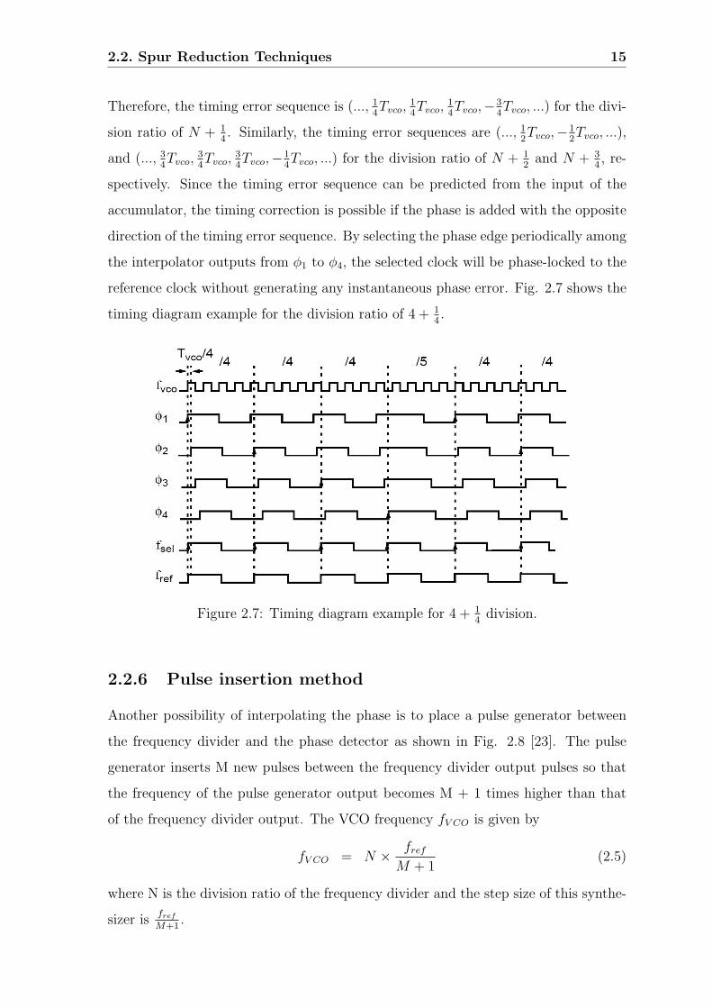
2.7 Timing diagram example for 4 + 14
division. . . . . . . . . . . . . . . 15
2.8 Pulse insertion method. . . . . . . . . . . . . . . . . . . . . . . . . . . 16
3.1 Phase Frequency Detector. . . . . . . . . . . . . . . . . . . . . . . . . 18
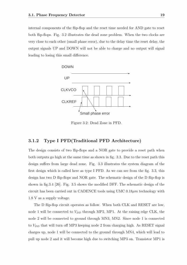
3.2 Dead Zone in PFD. . . . . . . . . . . . . . . . . . . . . . . . . . . . . 19
3.3 Type I PFD. . . . . . . . . . . . . . . . . . . . . . . . . . . . . . . . . 20
3.4 Traditional DFF. . . . . . . . . . . . . . . . . . . . . . . . . . . . . . 21
3.5 Modified DFF. . . . . . . . . . . . . . . . . . . . . . . . . . . . . . . 22
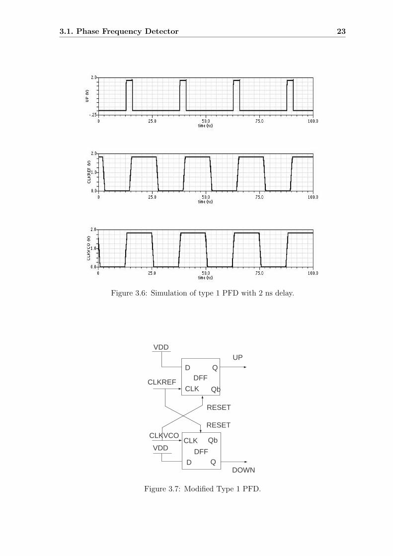
3.6 Simulation of type 1 PFD with 2 ns delay. . . . . . . . . . . . . . . . 23
3.7 Modified Type 1 PFD. . . . . . . . . . . . . . . . . . . . . . . . . . . 23
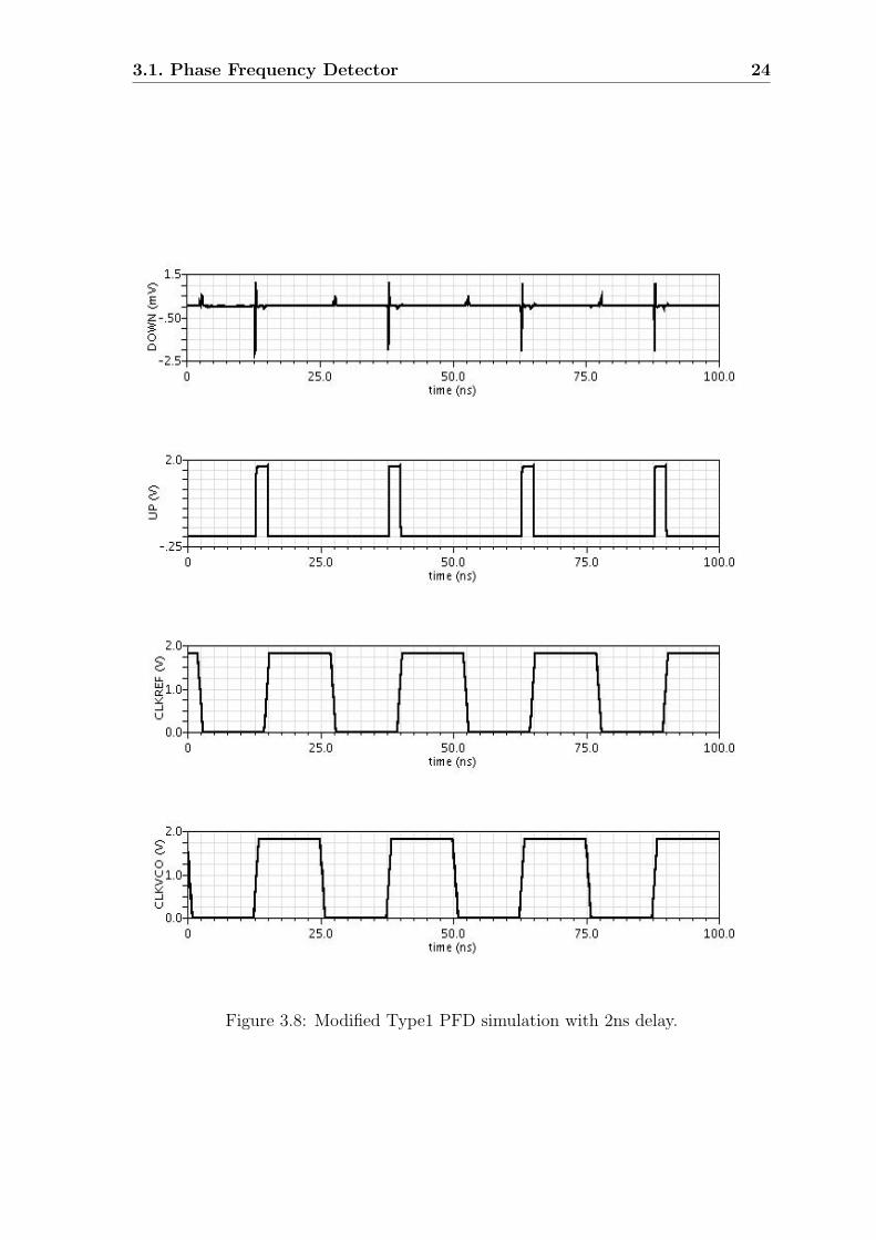
3.8 Modified Type1 PFD simulation with 2ns delay. . . . . . . . . . . . . 24
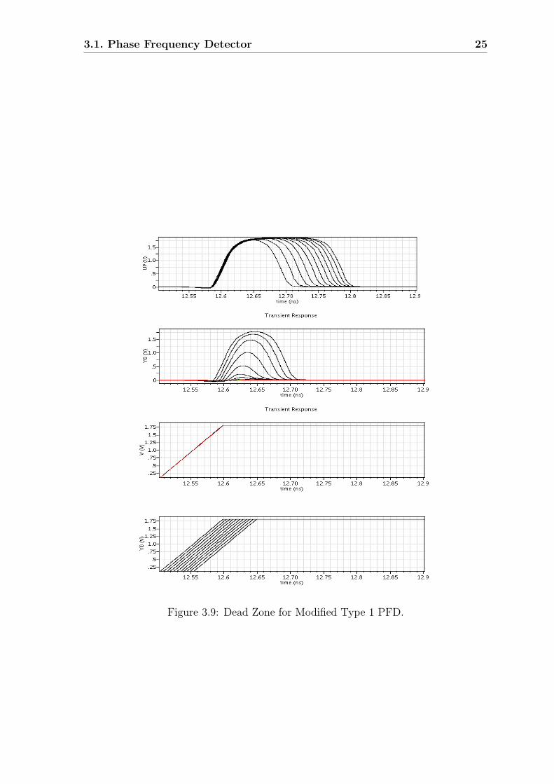
3.9 Dead Zone for Modified Type 1 PFD. . . . . . . . . . . . . . . . . . . 25
3.10 Schematic of Type 2 PFD. . . . . . . . . . . . . . . . . . . . . . . . . 26
3.11 Type2 PFD simulation with 2ns delay. . . . . . . . . . . . . . . . . . 27
3.12 Dead Zone in Type 2 PFD. . . . . . . . . . . . . . . . . . . . . . . . 28
3.13 Charge Pump [23] . . . . . . . . . . . . . . . . . . . . . . . . . . . . . 29
3.14 Schematic Design of Charge Pump. . . . . . . . . . . . . . . . . . . . 30
3.15 PFD-CP Simulation for 450 phase error. . . . . . . . . . . . . . . . . 31
v
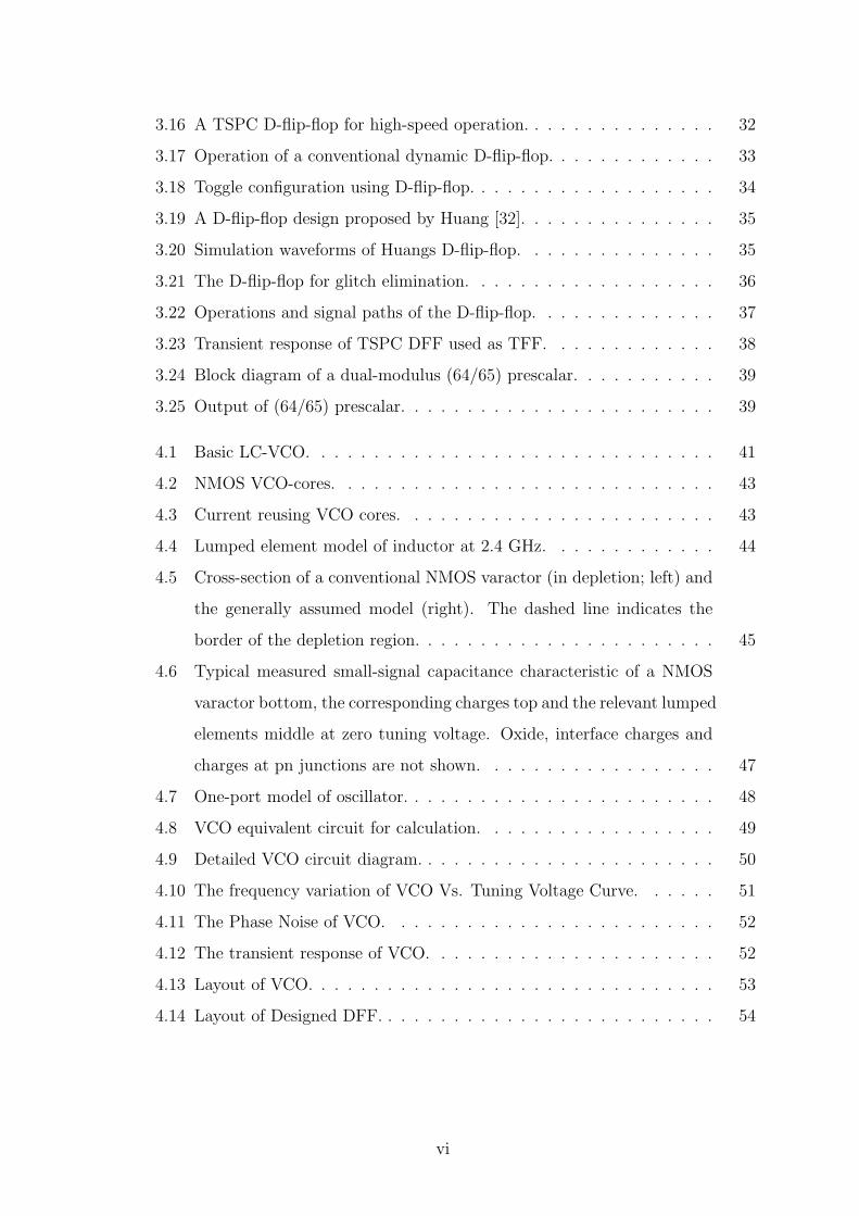
3.16 A TSPC D-flip-flop for high-speed operation. . . . . . . . . . . . . . . 32
3.17 Operation of a conventional dynamic D-flip-flop. . . . . . . . . . . . . 33
3.18 Toggle configuration using D-flip-flop. . . . . . . . . . . . . . . . . . . 34
3.19 A D-flip-flop design proposed by Huang [32]. . . . . . . . . . . . . . . 35
3.20 Simulation waveforms of Huangs D-flip-flop. . . . . . . . . . . . . . . 35
3.21 The D-flip-flop for glitch elimination. . . . . . . . . . . . . . . . . . . 36
3.22 Operations and signal paths of the D-flip-flop. . . . . . . . . . . . . . 37
3.23 Transient response of TSPC DFF used as TFF. . . . . . . . . . . . . 38
3.24 Block diagram of a dual-modulus (64/65) prescalar. . . . . . . . . . . 39
3.25 Output of (64/65) prescalar. . . . . . . . . . . . . . . . . . . . . . . . 39
4.1 Basic LC-VCO. . . . . . . . . . . . . . . . . . . . . . . . . . . . . . . 41
4.2 NMOS VCO-cores. . . . . . . . . . . . . . . . . . . . . . . . . . . . . 43
4.3 Current reusing VCO cores. . . . . . . . . . . . . . . . . . . . . . . . 43
4.4 Lumped element model of inductor at 2.4 GHz. . . . . . . . . . . . . 44
4.5 Cross-section of a conventional NMOS varactor (in depletion; left) and
the generally assumed model (right). The dashed line indicates the
border of the depletion region. . . . . . . . . . . . . . . . . . . . . . . 45
4.6 Typical measured small-signal capacitance characteristic of a NMOS
varactor bottom, the corresponding charges top and the relevant lumped
elements middle at zero tuning voltage. Oxide, interface charges and
charges at pn junctions are not shown. . . . . . . . . . . . . . . . . . 47
4.7 One-port model of oscillator. . . . . . . . . . . . . . . . . . . . . . . . 48
4.8 VCO equivalent circuit for calculation. . . . . . . . . . . . . . . . . . 49
4.9 Detailed VCO circuit diagram. . . . . . . . . . . . . . . . . . . . . . . 50
4.10 The frequency variation of VCO Vs. Tuning Voltage Curve. . . . . . 51
4.11 The Phase Noise of VCO. . . . . . . . . . . . . . . . . . . . . . . . . 52
4.12 The transient response of VCO. . . . . . . . . . . . . . . . . . . . . . 52
4.13 Layout of VCO. . . . . . . . . . . . . . . . . . . . . . . . . . . . . . . 53
4.14 Layout of Designed DFF. . . . . . . . . . . . . . . . . . . . . . . . . . 54
vi
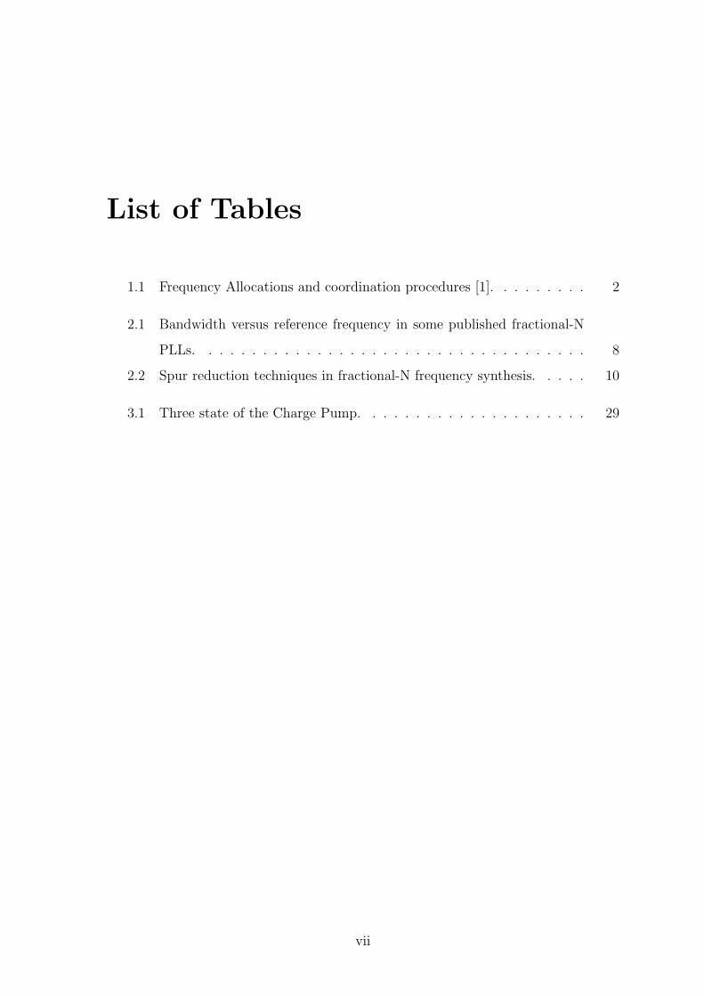
List of Tables
1.1 Frequency Allocations and coordination procedures [1]. . . . . . . . . 2
2.1 Bandwidth versus reference frequency in some published fractional-N
PLLs. . . . . . . . . . . . . . . . . . . . . . . . . . . . . . . . . . . . 8
2.2 Spur reduction techniques in fractional-N frequency synthesis. . . . . 10
3.1 Three state of the Charge Pump. . . . . . . . . . . . . . . . . . . . . 29
vii
Chapter 1
Introduction
With the explosive growth of the wireless communication industry, research related
to communication circuits and architectures has received a great deal of attention.
The major challenges are low-cost, low-voltage, and low-power designs, which com-
bine necessary performance with the ability to be manufactured economically in high
volumes. Recently, there has been an additional emphasis on integration of hetero-
geneous parts that constitute a communication transceiver. Modern transceivers are
expected to operate over a wide range of frequencies.
One of the most famous mobile broadcast system is Digital Video Broadcasting
Satellite services to Handhelds (DVB-SH). DVB-SH is a mobile broadcast standard
designed to deliver video, audio and data services to small handheld devices such
as mobile telephones, and vehicle-mounted devices. The key feature of DVB-SH
is the fact that it is a hybrid satellite/terrestrial system that will allow the use of
a satellite to achieve coverage of large regions or even a whole country. In areas
where direct reception of the satellite signal is impaired, and for indoor reception,
terrestrial repeaters are used to improve service availability. The DVB-SH system was
designed for frequencies below 3 GHz, supporting UHF band, L Band or S-band. It
complements and improves the existing DVB-H physical layer standard. Like (DVB-
H), it is based on DVB IP Datacast (IPDC) delivery, electronic service guides and
service purchase and protection standards.
DVB-SH specifies two operational modes:
1. SH-A: specifies the use of COFDM modulation on both satellite and terrestrial
1
2
links with the possibility of running both links in SFN mode.
2. SH-B: uses Time-Division Multiplexing (TDM) on the satellite link and COFDM
on the terrestrial link.
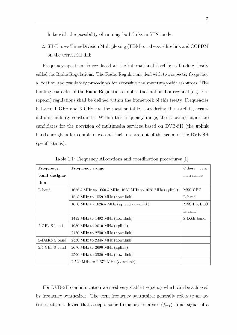
Frequency spectrum is regulated at the international level by a binding treaty
called the Radio Regulations. The Radio Regulations deal with two aspects: frequency
allocation and regulatory procedures for accessing the spectrum/orbit resources. The
binding character of the Radio Regulations implies that national or regional (e.g. Eu-
ropean) regulations shall be defined within the framework of this treaty. Frequencies
between 1 GHz and 3 GHz are the most suitable, considering the satellite, termi-
nal and mobility constraints. Within this frequency range, the following bands are
candidates for the provision of multimedia services based on DVB-SH (the uplink
bands are given for completeness and their use are out of the scope of the DVB-SH
specifications).
Table 1.1: Frequency Allocations and coordination procedures [1].
Frequency
band designa-
tion
Frequency range Others com-
mon names
L band 1626.5 MHz to 1660.5 MHz, 1668 MHz to 1675 MHz (uplink) MSS GEO
1518 MHz to 1559 MHz (downlink) L band
1610 MHz to 1626.5 MHz (up and downlink) MSS Big LEO
L band
1452 MHz to 1492 MHz (downlink) S-DAB band
2 GHz S band 1980 MHz to 2010 MHz (uplink)
2170 MHz to 2200 MHz (downlink)
S-DARS S band 2320 MHz to 2345 MHz (downlink)
2.5 GHz S band 2670 MHz to 2690 MHz (uplink)
2500 MHz to 2520 MHz (downlink)
2 520 MHz to 2 670 MHz (downlink)
For DVB-SH communication we need very stable frequency which can be achieved
by frequency synthesizer. The term frequency synthesizer generally refers to an ac-
tive electronic device that accepts some frequency reference (fref ) input signal of a
3
very stable frequency and then generates the desired frequency output, whereby the
stability, accuracy, and spectral purity of the output correlate with the performance
of the input reference.
Frequency synthesizers typically come in three main types:
1. The table-look-up synthesizer.
2. The direct synthesizer.
3. The indirect or phase-locked loop synthesizer.
In a table look- up synthesizer or digital synthesizer, the sinusoidal waveform
is created piece by piece by using the digital values of the waveform stored in a
memory. The hardware needed is a digital accumulator, whose capacity determines
the frequency resolution, a memory containing a cosine, a digital-to-analog converter
(DAC) and a low-pass filter to remove high-frequency spurs. Due to the limited speed
of the memory and the high-resolution DAC, high frequency operation is not feasible.
Moreover, high-frequency spurious tones tend to corrupt the spectral purity. The
direct synthesizer synthesizes the wanted output frequency from a single reference by
multiplying, mixing and dividing. By repeatedly mixing and dividing any frequency
accuracy is attainable. Ideally, the output spectrum is as clean as the reference
spectrum and fast frequency hopping is possible. However, when implementing the
direct synthesizer, cross-coupling between stages is a serious problem for the spectral
purity and the large number of components causes the synthesizer to be very bulky
and power consuming.
The indirect frequency synthesizer generates its output by phase-locking the di-
vided output to a reference signal. The phase-locked loop frequency synthesizer has
the potential of combining high frequency and low power. But its most distinct ad-
vantage is that the phase-locked loop is very well suited for integration in low-cost IC
processes, like CMOS. This is the reason why the PLL is used for frequency synthesis
in almost all wireless communication chip sets on the market.
The phase-locked loop synthesizer is the main topic of this work.
Fractional-N synthesis refers to the synthesis of a reference frequency that is related
with a fractional ratio to another reference frequency. This is especially important
4
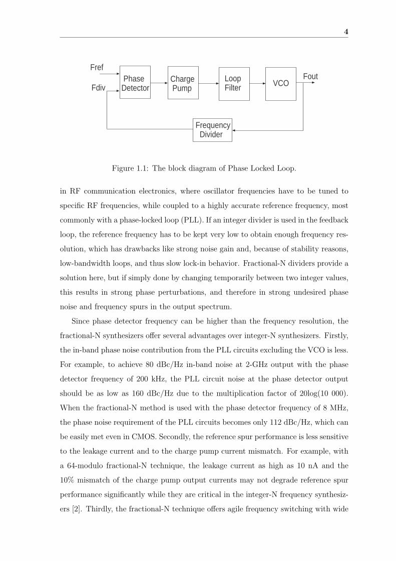
Frequency Divider
PhaseDetector
Charge Pump
LoopFilter VCO
FoutFdiv
Fref
Figure 1.1: The block diagram of Phase Locked Loop.
in RF communication electronics, where oscillator frequencies have to be tuned to
specific RF frequencies, while coupled to a highly accurate reference frequency, most
commonly with a phase-locked loop (PLL). If an integer divider is used in the feedback
loop, the reference frequency has to be kept very low to obtain enough frequency res-
olution, which has drawbacks like strong noise gain and, because of stability reasons,
low-bandwidth loops, and thus slow lock-in behavior. Fractional-N dividers provide a
solution here, but if simply done by changing temporarily between two integer values,
this results in strong phase perturbations, and therefore in strong undesired phase
noise and frequency spurs in the output spectrum.
Since phase detector frequency can be higher than the frequency resolution, the
fractional-N synthesizers offer several advantages over integer-N synthesizers. Firstly,
the in-band phase noise contribution from the PLL circuits excluding the VCO is less.
For example, to achieve 80 dBc/Hz in-band noise at 2-GHz output with the phase
detector frequency of 200 kHz, the PLL circuit noise at the phase detector output
should be as low as 160 dBc/Hz due to the multiplication factor of 20log(10 000).
When the fractional-N method is used with the phase detector frequency of 8 MHz,
the phase noise requirement of the PLL circuits becomes only 112 dBc/Hz, which can
be easily met even in CMOS. Secondly, the reference spur performance is less sensitive
to the leakage current and to the charge pump current mismatch. For example, with
a 64-modulo fractional-N technique, the leakage current as high as 10 nA and the
10% mismatch of the charge pump output currents may not degrade reference spur
performance significantly while they are critical in the integer-N frequency synthesiz-
ers [2]. Thirdly, the fractional-N technique offers agile frequency switching with wide
1.1. Problem Definition and Methodology 5
loop bandwidth. Some applications employ narrow band fractional-N synthesizers
simply to alleviate the PLL noise contribution. In that case, faster settling time can
be achieved by using a dynamic bandwidth method. By dynamic bandwidth we mean
that the loop bandwidth is set to be wider than the desired one when the PLL is in
the frequency acquisition mode [3][4]. With high phase detector frequency, the loop
bandwidth in the transient mode can be set high with less overshoot problem. The
fractional-N technique provides the opportunity of using dynamic bandwidth methods
more effectually.
1.1 Problem Definition and Methodology
The design of Fractional-N frequency synthesizer using PLL is taken up for study.
Since the Fractional-N frequency synthesizer have many advantages over other syn-
thesizer. The only disadvantage of fractional-N frequency synthesizer is the Spur,
which have to be suppressed using different techniques, which will increase the cir-
cuit complexity. This work is intended towards the design of complete fractional-N
frequency synthesizer.
CADENCE tools are followed for circuit simulation. Composer-schematic by CA-
DENCE tools is used for drawing schematic and Virtuoso is used for simulating the
design. The layout will be carried out using CADENCE design flow targeting UMC
foundry through Euro-practice for chip fabrication.
1.2 Thesis organization
In chapter two, the literature survey of Fractional-N frequency synthesizer is pre-
sented. Different spur reduction techniques like DAC estimation, Random jittering,
modulator, phase interpolation, phase compensation and phase insertion are discussed
in detail. A state of the art comparison of various architecture is provided at the end.
In chapter three, the design of different blocks of synthesizer are presented, like
Phase Frequency detector and charge pump. The simulation results of those design
are also presented at the end of design of each block. These designs are carried out
in CADENCE tools with the 0.18 m Technology provided by UMC foundry.
1.2. Thesis organization 6
In chapter four, the design of 2.4 GHz VCO is carried out. First the discussion on
different architecture of VCO is presented. Then the useful component are discussed
like Varactor and inductor. The simulation result of VCO is given at the end of this
chapter.
In chapter five the thesis is concluded with the future work to be done.
Chapter 2
Overview of Frequency Synthesizer
In the traditional Integer synthesizer, the voltage-controlled oscillator (VCO) fre-
quency is at some integer multiple of the reference frequency fref ). Frequency steps
smaller than fref are not possible. As a result, the comparison frequency can be no
higher, in frequency, than the desired channel spacing, or step size. If the VCO fre-
quency is high, and the step size is small, this results in a large division ratio in the
VCO path.
In a normal synthesizer, while locked, the phase detector produces a narrow pulse,
which is required to keep the VCO on frequency. Each pulse from the phase detector
should be identical to all the other pulses.
In the fractional N loop, the VCO is never quite on frequency. That is, it is never
an exact integer multiple of the comparison frequency. In one cycle of the comparison
frequency the VCO frequency will appear to be high by half the comparison frequency.
In the next cycle, the VCO will appear to be low by an equal amount. The loop will
therefore attempt to ramp the VCO frequency up, then down in alternate cycles of
the phase detector, creating a spur at half the comparison frequency. Because this
spur occurs at a fraction of the comparison frequency, it is known as a fractional spur.
It will be shown later that the chips used to develop this technique contain some
additional circuitry to minimize the level of the fractional spurs.
7
2.1. Fractional-N Frequency Synthesis 8
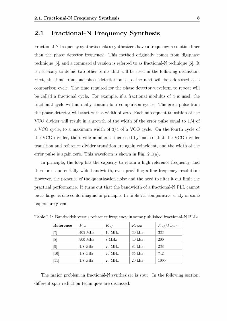
2.1 Fractional-N Frequency Synthesis
Fractional-N frequency synthesis makes synthesizers have a frequency resolution finer
than the phase detector frequency. This method originally comes from digiphase
technique [5], and a commercial version is referred to as fractional-N technique [6]. It
is necessary to define two other terms that will be used in the following discussion.
First, the time from one phase detector pulse to the next will be addressed as a
comparison cycle. The time required for the phase detector waveform to repeat will
be called a fractional cycle. For example, if a fractional modulus of 4 is used, the
fractional cycle will normally contain four comparison cycles. The error pulse from
the phase detector will start with a width of zero. Each subsequent transition of the
VCO divider will result in a growth of the width of the error pulse equal to 1/4 of
a VCO cycle, to a maximum width of 3/4 of a VCO cycle. On the fourth cycle of
the VCO divider, the divide number is increased by one, so that the VCO divider
transition and reference divider transition are again coincident, and the width of the
error pulse is again zero. This waveform is shown in Fig. 2.1(a).
In principle, the loop has the capacity to retain a high reference frequency, and
therefore a potentially wide bandwidth, even providing a fine frequency resolution.
However, the presence of the quantization noise and the need to filter it out limit the
practical performance. It turns out that the bandwidth of a fractional-N PLL cannot
be as large as one could imagine in principle. In table 2.1 comparative study of some
papers are given.
Table 2.1: Bandwidth versus reference frequency in some published fractional-N PLLs.
Reference Fout Fref F−3dB Fref/F−3dB
[7] 405 MHz 10 MHz 30 kHz 333
[8] 900 MHz 8 MHz 40 kHz 200
[9] 1.8 GHz 20 MHz 84 kHz 238
[10] 1.8 GHz 26 MHz 35 kHz 742
[11] 1.8 GHz 20 MHz 20 kHz 1000
The major problem in fractional-N synthesizer is spur. In the following section,
different spur reduction techniques are discussed.
2.2. Spur Reduction Techniques 9
PhaseDetector
Charge Pump VCO
FoutFdiv
Fref
/(N / N+1)
LPF
P
K-bitAccumulator
Fref
(a) Block Diagram
(b) Timing Diagram
Figure 2.1: Fractional-N frequency synthesis.
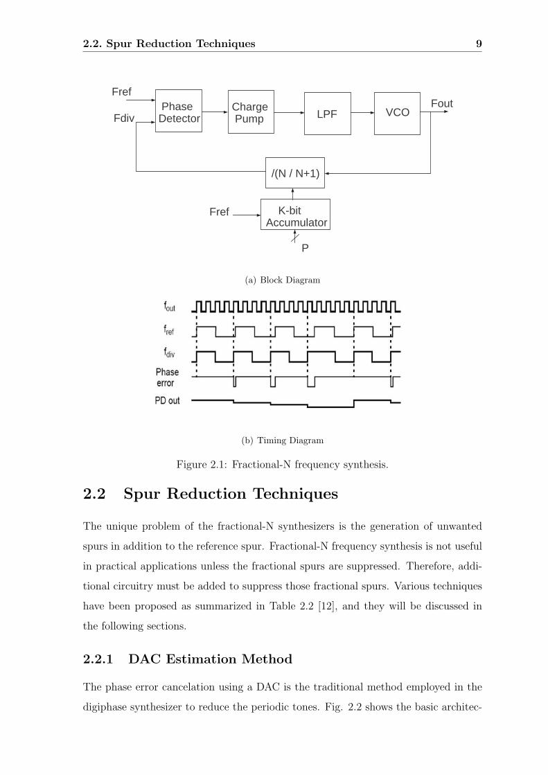
2.2 Spur Reduction Techniques
The unique problem of the fractional-N synthesizers is the generation of unwanted
spurs in addition to the reference spur. Fractional-N frequency synthesis is not useful
in practical applications unless the fractional spurs are suppressed. Therefore, addi-
tional circuitry must be added to suppress those fractional spurs. Various techniques
have been proposed as summarized in Table 2.2 [12], and they will be discussed in
the following sections.
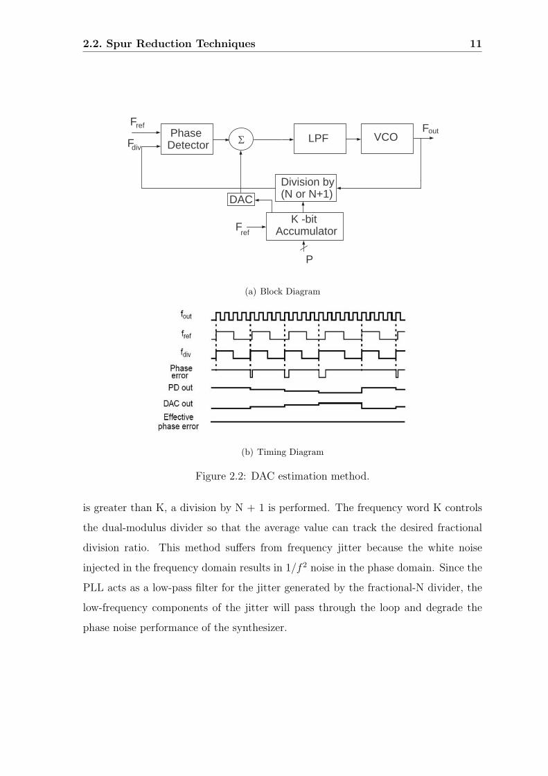
2.2.1 DAC Estimation Method
The phase error cancelation using a DAC is the traditional method employed in the
digiphase synthesizer to reduce the periodic tones. Fig. 2.2 shows the basic architec-
2.2. Spur Reduction Techniques 10
Table 2.2: Spur reduction techniques in fractional-N frequency synthesis.
Techniques Features Problems
DAC estimation Cancels spur by DAC Analog mismatches
Random jittering Randomizes divider control Frequency jitter
∆− Σ modulation Modulates divider control with
noise shaping
Quantization noise at high fre-
quencies
Phase interpolation Inherent fractional division Multi-phase VCO
Phase compensation Time-domain compensation Analog mismatches
Pulse insertion Frequency multiplier using pulse
insertion
Analog mismatches
ture and its operation. The value of the accumulator carries the information of the
spurious beat tone, which allows the DAC to predict the phase error for cancelation.
synthesizer that operates from 40 to 51 MHz with a reference frequency of 100 kHz
using this technique has been reported to exhibit a resolution of 1 Hz and spurious
sidebands less than -70 dBc [13]. Since the phase error is compensated in the voltage
domain, this method suffers from analog imperfections. The mismatch results primar-
ily from limited DAC resolution and the limited accuracy of the DAC. This approach
is effective when a sample-and-hold (S/H) phase detector is used. For the S/H phase
detector, the DAC needs to match only the dc voltage during one reference clock
period. For the phase-and-frequency detector (P/FD) that is widely used in modern
PLL ICs, the DAC must generate a waveform to match the real-time phase detector
output, and its performance is not sufficient to obtain the wide loop bandwidth [14].
2.2.2 Random Jittering Method
The spur in the fractional-N synthesizer originates from the fixed pattern of the dual
modulus divider. This periodicity in the control sequence of the dual-modulus divider
can be eliminated by random jitter injection. While the phase estimation technique
using a DAC operates in the analog domain, the random jittering approach solves the
spur problem in the digital domain. Fig. 2.3 shows a block diagram of a fractional-
N divider with random jittering [15]. At every output of the divider, the random or
pseudo random number generator produces a new random word Pn which is compared
with the frequency word K. If Pn is less than K, a division by N is performed. If Pn
2.2. Spur Reduction Techniques 11
PhaseDetector LPF VCO
Fout
Division by (N or N+1)
K -bit Accumulator
P
F
F
Fdiv
ref
ref
Σ
DAC
(a) Block Diagram
(b) Timing Diagram
Figure 2.2: DAC estimation method.
is greater than K, a division by N + 1 is performed. The frequency word K controls
the dual-modulus divider so that the average value can track the desired fractional
division ratio. This method suffers from frequency jitter because the white noise
injected in the frequency domain results in 1/f 2 noise in the phase domain. Since the
PLL acts as a low-pass filter for the jitter generated by the fractional-N divider, the
low-frequency components of the jitter will pass through the loop and degrade the
phase noise performance of the synthesizer.
2.2. Spur Reduction Techniques 12
PhaseDetector LPF VCO
Fout
Division by (N or N+1)
F
Fdiv
ref
N-bit word comparator
Random Number Generator
P
Fref
n
Figure 2.3: Random jittering method.
2.2.3 ∆− Σ Modulation method
Another method is using an over sampling ∆−Σ modulator to interpolate fractional
frequency with a coarse integer divider as shown in Fig. 2.4 [16][17]. Since the second
order or higher ∆ − Σ modulators do not generate fixed tones for dc inputs, they
effectively shape the phase noise without causing any spur. This method is similar to
the random jittering method, but it does not generate a frequency jitter due to the
noise-shaping property of the ∆− Σ modulator.
The conventional digiphase technique suffers from poor fractional spur perfor-
mance due to imperfect analog matching. It is difficult for charge-pump PLLs to
achieve high output frequency since the ratio of the phase compensation current to
the charge-pump current becomes very small. Typically, the synthesizers with out-
put frequency higher than 2-GHz have the fractional modulo of at most 8 for that
reason. The digiphase technique also requires specific crystal frequency range since it
provides only finite fractional modulo of 2N, where N is the number of bits used for
the accumulator.
The ∆− Σ fractional-N synthesizer offers agile switching and arbitrarily fine fre-
quency resolution that can make the synthesizer compensate for crystal-frequency
drift with a digital word and accommodate various crystal frequencies without re-
ducing phase detector frequency [18][19]. This synthesizer also alleviates PLL design
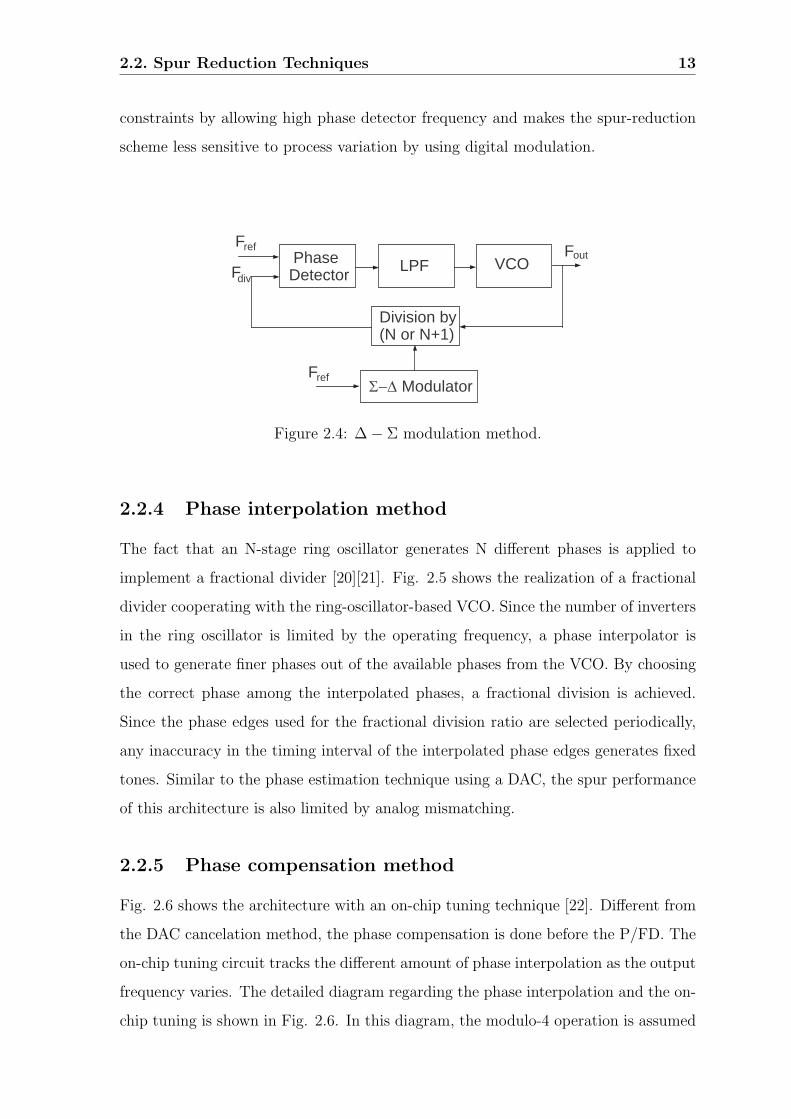
2.2. Spur Reduction Techniques 13
constraints by allowing high phase detector frequency and makes the spur-reduction
scheme less sensitive to process variation by using digital modulation.
PhaseDetector LPF VCO
Fout
Division by (N or N+1)
F
Fdiv
ref
Σ−Δ ModulatorFref
Figure 2.4: ∆− Σ modulation method.
2.2.4 Phase interpolation method
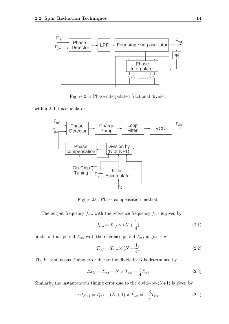
The fact that an N-stage ring oscillator generates N different phases is applied to
implement a fractional divider [20][21]. Fig. 2.5 shows the realization of a fractional
divider cooperating with the ring-oscillator-based VCO. Since the number of inverters
in the ring oscillator is limited by the operating frequency, a phase interpolator is
used to generate finer phases out of the available phases from the VCO. By choosing
the correct phase among the interpolated phases, a fractional division is achieved.
Since the phase edges used for the fractional division ratio are selected periodically,
any inaccuracy in the timing interval of the interpolated phase edges generates fixed
tones. Similar to the phase estimation technique using a DAC, the spur performance
of this architecture is also limited by analog mismatching.
2.2.5 Phase compensation method
Fig. 2.6 shows the architecture with an on-chip tuning technique [22]. Different from
the DAC cancelation method, the phase compensation is done before the P/FD. The
on-chip tuning circuit tracks the different amount of phase interpolation as the output
frequency varies. The detailed diagram regarding the phase interpolation and the on-
chip tuning is shown in Fig. 2.6. In this diagram, the modulo-4 operation is assumed
2.2. Spur Reduction Techniques 14
PhaseDetector LPF Four stage ring oscillator
Fout
/N
F
Fdiv
ref
PhaseInterpolator
Figure 2.5: Phase-interpolated fractional divider.
with a 2- bit accumulator.
PhaseDetector
Charge Pump
LoopFilter VCO
Fout
Division by (N or N+1)
K -bit Accumulator
K
F
F
Fdiv
ref
ref
Phasecompensation
On-Chip Tuning
Figure 2.6: Phase compensation method.
The output frequency fvco with the reference frequency fref is given by
fvco = fref × (N +1
4) (2.1)
or the output period Tvco with the reference period Tref is given by
Tref = Tvco × (N +1
4) (2.2)
The instantaneous timing error due to the divide-by-N is determined by
4tN = Tref −N × Tvco =1
4Tvco (2.3)
Similarly, the instantaneous timing error due to the divide-by-(N+1) is given by
4tN+1 = Tref − (N + 1)× Tvco = −3
4Tvco (2.4)
2.2. Spur Reduction Techniques 15
Therefore, the timing error sequence is (..., 14Tvco,
14Tvco,
14Tvco,−3
4Tvco, ...) for the divi-
sion ratio of N + 14. Similarly, the timing error sequences are (..., 1
2Tvco,−1
2Tvco, ...),
and (..., 34Tvco,
34Tvco,
34Tvco,−1
4Tvco, ...) for the division ratio of N + 1
2and N + 3
4, re-
spectively. Since the timing error sequence can be predicted from the input of the
accumulator, the timing correction is possible if the phase is added with the opposite
direction of the timing error sequence. By selecting the phase edge periodically among
the interpolator outputs from φ1 to φ4, the selected clock will be phase-locked to the
reference clock without generating any instantaneous phase error. Fig. 2.7 shows the
timing diagram example for the division ratio of 4 + 14.
Figure 2.7: Timing diagram example for 4 + 14
division.
2.2.6 Pulse insertion method
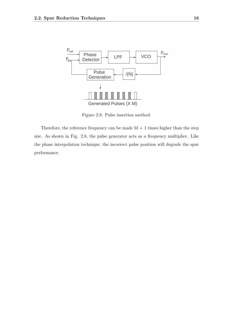
Another possibility of interpolating the phase is to place a pulse generator between
the frequency divider and the phase detector as shown in Fig. 2.8 [23]. The pulse
generator inserts M new pulses between the frequency divider output pulses so that
the frequency of the pulse generator output becomes M + 1 times higher than that
of the frequency divider output. The VCO frequency fV CO is given by
fV CO = N × fref
M + 1(2.5)
where N is the division ratio of the frequency divider and the step size of this synthe-
sizer isfref
M+1.
2.2. Spur Reduction Techniques 16
PhaseDetector LPF VCO
Fout
/(N)
F
Fdiv
ref
PulseGeneration
Generated Pulses (X M)
Figure 2.8: Pulse insertion method.
Therefore, the reference frequency can be made M + 1 times higher than the step
size. As shown in Fig. 2.8, the pulse generator acts as a frequency multiplier. Like
the phase interpolation technique, the incorrect pulse position will degrade the spur
performance.
Chapter 3
Design of individual circuit blocks
of synthesizer
3.1 Phase Frequency Detector
3.1.1 PFD based on DFF
In this section we discussed the three types of PFD implementation i.e. traditional,
Type I PFD and Type II PFD. Phase frequency detector (PFD) is one of the impor-
tant parts in PLL circuits. PFD is a circuit that measures the phase and frequency
difference between two signals, i.e. the signal that comes from the VCO and the ref-
erence signal. PFD has two outputs UP and DOWN which are signaled according to
the phase and frequency difference of the input signals.
The output signals of the PFD are fed to the charge pump. The output voltage of
the charge pump controls the output frequency of the VCO, so with a change happens
at the input of the CP the output voltage will change which will change the output
frequency of the VCO [24]. In this case the sensitivity of the phase and frequency
difference detection of the PFD is very crucial. Sensitivity of the PFD means the
smallest difference the PFD can detect and produce UP or DOWN signals that will
affect the charge pump, this lead to the conclusion that the higher the sensitivity the
better the PFD. One of the disadvantages that PFD suffers is dead-zone. Dead-zone
is a small difference in the phase of the inputs that a PFD will not be able to detect.
Dead zone is due to the delay time of the logic components and rest of the feedback
17
3.1. Phase Frequency Detector 18
path of the flip flops.
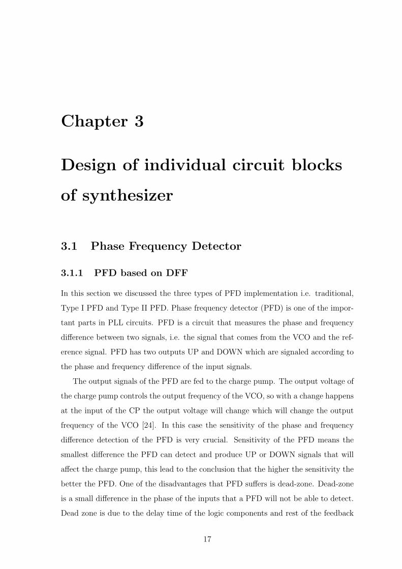
Fig. 3.1, shows a detailed design for PFD with input/output signals transaction. A
simple design of PFD consists of two D flip flops and AND gate. As the fig. 3.1 shows
the D input of the flip-flops is connected to VDD and the input signals (CLKREF,
CLKVCO) are applied to the clock input. When one of the clocks change to high, this
flip-flop will charged and change its output to high. The AND gate is for preventing
both flip-flop to be high at the same time. As we can see the inputs of the AND
gate are the both Up and DOWN signal from both flip-flops, and the output of the
AND gate is connected to the reset input of the flip-flops. As soon as both outputs
(UP, DOWN) are high the AND gate will generate a high signal that will reset both
flip-flops avoiding the situation of both high at the same time. The signal transaction
in fig. 3.1 gives an example of CLKREF leading CLKVCO.
DFFD
CLK
Q
Qb
DFFD
CLK Q
Qb
RESET
RESET
DOWN
UP
CLKREF
CLKVCO
VDD
VDD
(a) Block Diagram
DOWN
UP
CLKVCO
CLKREF
(b) Signal TransactionFigure 3.1: Phase Frequency Detector.
From the transaction, once CLKREF goes high it will charge the flip-flop and
charges UP signal to high. When CLKVCO becomes high it will change DOWN
signal to high. This will lead to have both output at high which will let the AND gate
to signal the reset output and reset both flip-flops driving both outputs to low. Since
CLKREF is leading in fig. 3.1, we can notice that only UP signal is signaling when
CLKREF change to high. in case CLKVCO is leading the opposite is true, which
means DOWN signal will be high when CLKVCO change to high.
As we mentioned before, dead-zone is due to small phase error. When the phase
difference between PFDs input signals, the output signals of the PFD will not be
proportional to this error [25]. The reason of this problem is the delay time of the
3.1. Phase Frequency Detector 19
internal components of the flip-flop and the reset time needed for AND gate to reset
both flip-flops. Fig. 3.2 illustrates the dead zone problem. When the two clocks are
very close to each other (small phase error), due to the delay time the reset delay, the
output signals UP and DOWN will not be able to charge and no output will signal
leading to losing this small difference.
Small phase error
CLKREF
CLKVCO
UP
DOWN
Figure 3.2: Dead Zone in PFD.
3.1.2 Type I PFD(Traditional PFD Architecture)
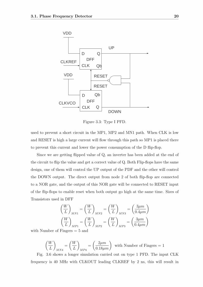
The design consists of two flip-flops and a NOR gate to provide a reset path when
both outputs go high at the same time as shown in fig. 3.3. Due to the reset path this
design suffers from large dead zone. Fig. 3.3 illustrates the system diagram of the
first design which is called here as type I PFD. As we can see from the fig. 3.3, this
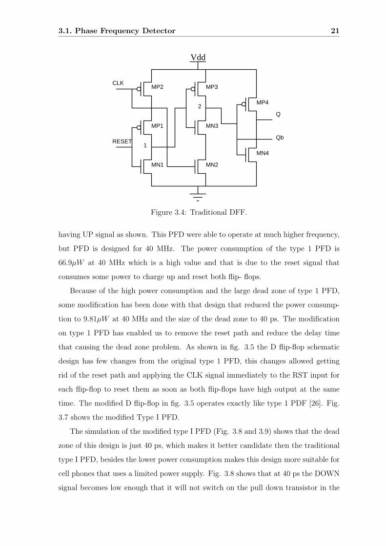
design has two D flip-flops and NOR gate. The schematic design of the D flip-flop is
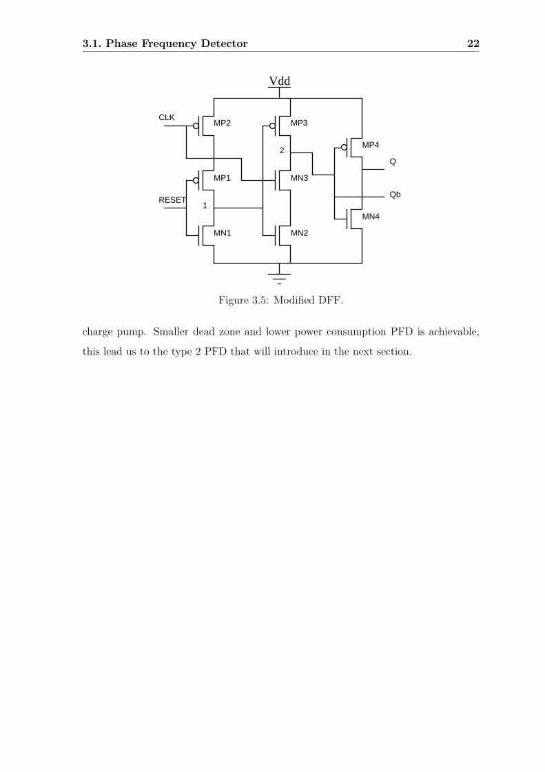
shown in fig.3.4 [26]. Fig. 3.5 shows the modified DFF. The schematic design of the
circuit has been carried out in CADENCE tools using UMC 0.18µm technology with
1.8 V as a supply voltage.
The D flip-flop circuit operates as follow. When both CLK and RESET are low,
node 1 will be connected to VDD through MP2, MP1. At the raising edge CLK, the
node 2 will be connected to ground through MN3, MN2. Since node 1 is connected
to VDD that will turn off MP3 keeping node 2 from charging high. As RESET signal
charges up, node 1 will be connected to the ground through MN4, which will lead to
pull up node 2 and it will become high due to switching MP3 on. Transistor MP1 is
3.1. Phase Frequency Detector 20
DFFD
CLK
Q
Qb
DFFD
CLK Q
Qb
RESET
RESET
DOWN
UP
CLKREF
CLKVCO
VDD
VDD
Figure 3.3: Type I PFD.
used to prevent a short circuit in the MP1, MP2 and MN1 path. When CLK is low
and RESET is high a large current will flow through this path so MP1 is placed there
to prevent this current and lower the power consumption of the D flip-flop.
Since we are getting flipped value of Q, an inverter has been added at the end of
the circuit to flip the value and get a correct value of Q. Both Flip-flops have the same
design, one of them will control the UP output of the PDF and the other will control
the DOWN output. The direct output from node 2 of both flip-flop are connected
to a NOR gate, and the output of this NOR gate will be connected to RESET input
of the flip-flops to enable reset when both output go high at the same time. Sizes of
Transistors used in DFF(W
L
)MN1
=
(W
L
)MN2
=
(W
L
)MN3
=
(3µm
0.4µm
)(W
L
)MP1
=
(W
L
)MP2
=
(W
L
)MP3
=
(3µm
0.4µm
)with Number of Fingers = 5 and
(W
L
)MN4
=
(W
L
)MP4
=
(2µm
0.18µm
)with Number of Fingers = 1
Fig. 3.6 shows a longer simulation carried out on type 1 PFD. The input CLK
frequency is 40 MHz with CLKOUT leading CLKREF by 2 ns, this will result in
3.1. Phase Frequency Detector 21
Vdd
CLK
RESET
MP2
MP1
MN1
MP3
MN3
MN2
MP4
MN4
Q
Qb
2
1
Figure 3.4: Traditional DFF.
having UP signal as shown. This PFD were able to operate at much higher frequency,
but PFD is designed for 40 MHz. The power consumption of the type 1 PFD is
66.9µW at 40 MHz which is a high value and that is due to the reset signal that
consumes some power to charge up and reset both flip- flops.
Because of the high power consumption and the large dead zone of type 1 PFD,
some modification has been done with that design that reduced the power consump-
tion to 9.81µW at 40 MHz and the size of the dead zone to 40 ps. The modification
on type 1 PFD has enabled us to remove the reset path and reduce the delay time
that causing the dead zone problem. As shown in fig. 3.5 the D flip-flop schematic
design has few changes from the original type 1 PFD, this changes allowed getting
rid of the reset path and applying the CLK signal immediately to the RST input for
each flip-flop to reset them as soon as both flip-flops have high output at the same
time. The modified D flip-flop in fig. 3.5 operates exactly like type 1 PDF [26]. Fig.
3.7 shows the modified Type I PFD.
The simulation of the modified type I PFD (Fig. 3.8 and 3.9) shows that the dead
zone of this design is just 40 ps, which makes it better candidate then the traditional
type I PFD, besides the lower power consumption makes this design more suitable for
cell phones that uses a limited power supply. Fig. 3.8 shows that at 40 ps the DOWN
signal becomes low enough that it will not switch on the pull down transistor in the
3.1. Phase Frequency Detector 22
Vdd
CLK
RESET
MP2
MP1
MN1
MP3
MN3
MN2
MP4
MN4
Q
Qb
2
1
Figure 3.5: Modified DFF.
charge pump. Smaller dead zone and lower power consumption PFD is achievable,
this lead us to the type 2 PFD that will introduce in the next section.
3.1. Phase Frequency Detector 23
Figure 3.6: Simulation of type 1 PFD with 2 ns delay.
DFFD
CLK
Q
Qb
DFFD
CLK
Q
Qb
RESET
RESET
DOWN
UP
CLKREF
CLKVCO
VDD
VDD
Figure 3.7: Modified Type 1 PFD.
3.1. Phase Frequency Detector 24
Figure 3.8: Modified Type1 PFD simulation with 2ns delay.
3.1. Phase Frequency Detector 25
Figure 3.9: Dead Zone for Modified Type 1 PFD.
3.1. Phase Frequency Detector 26
3.1.3 Type 2 PFD
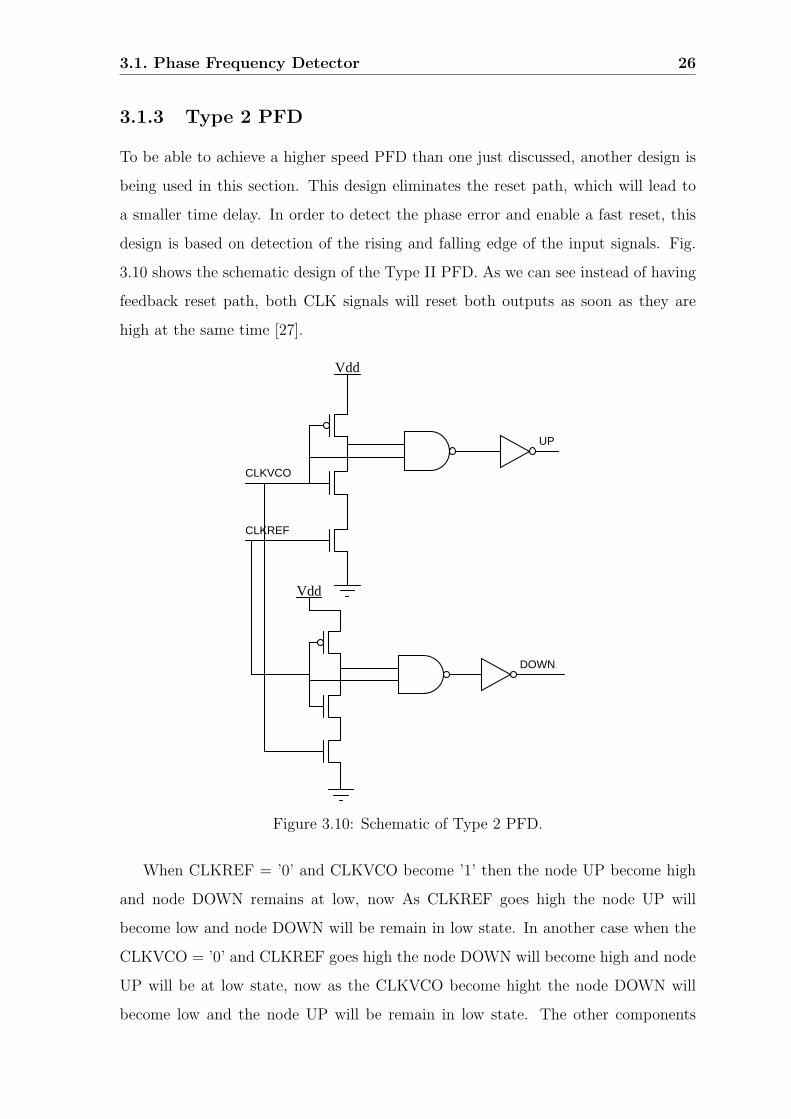
To be able to achieve a higher speed PFD than one just discussed, another design is
being used in this section. This design eliminates the reset path, which will lead to
a smaller time delay. In order to detect the phase error and enable a fast reset, this
design is based on detection of the rising and falling edge of the input signals. Fig.
3.10 shows the schematic design of the Type II PFD. As we can see instead of having
feedback reset path, both CLK signals will reset both outputs as soon as they are
high at the same time [27].
CLKVCO
CLKREF
Vdd
UP
Vdd
DOWN
Figure 3.10: Schematic of Type 2 PFD.
When CLKREF = ’0’ and CLKVCO become ’1’ then the node UP become high
and node DOWN remains at low, now As CLKREF goes high the node UP will
become low and node DOWN will be remain in low state. In another case when the
CLKVCO = ’0’ and CLKREF goes high the node DOWN will become high and node
UP will be at low state, now as the CLKVCO become hight the node DOWN will
become low and the node UP will be remain in low state. The other components
3.1. Phase Frequency Detector 27
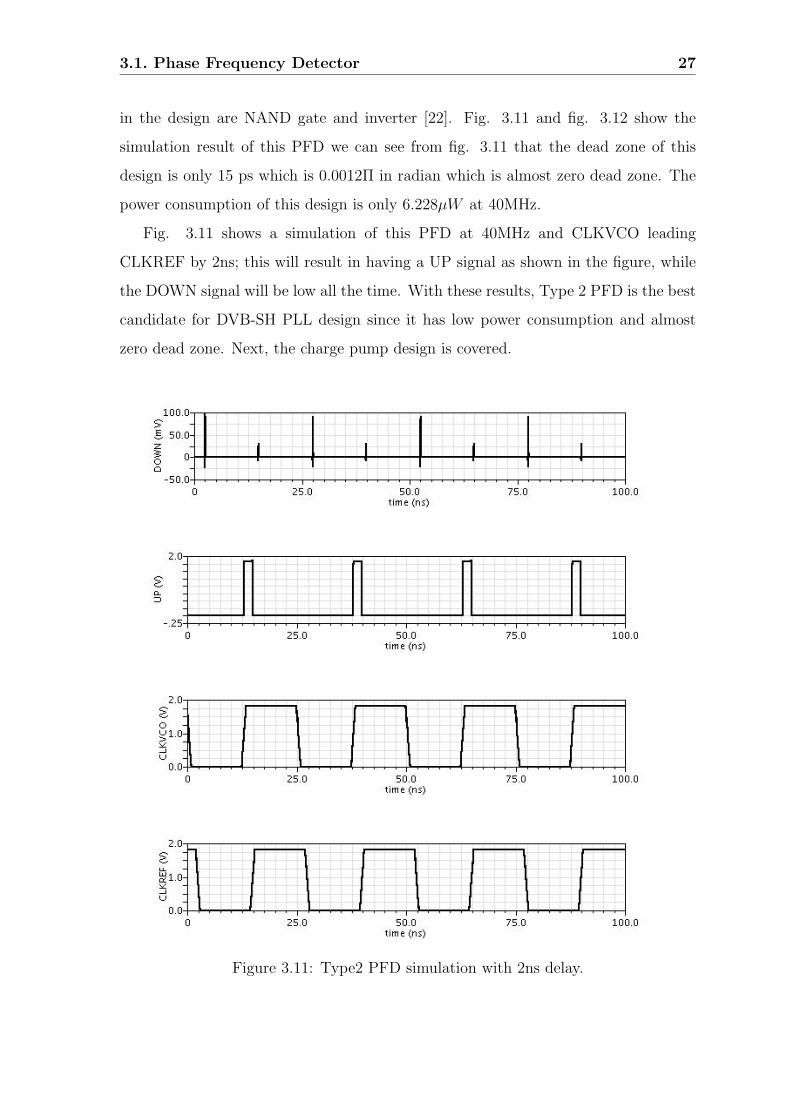
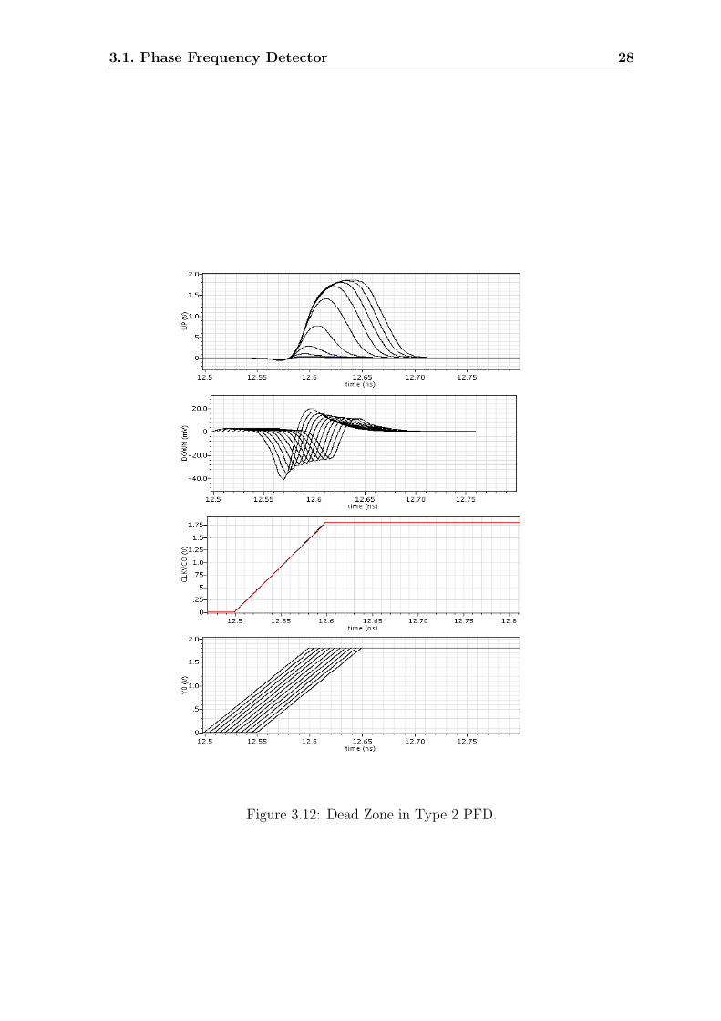
in the design are NAND gate and inverter [22]. Fig. 3.11 and fig. 3.12 show the
simulation result of this PFD we can see from fig. 3.11 that the dead zone of this
design is only 15 ps which is 0.0012Π in radian which is almost zero dead zone. The
power consumption of this design is only 6.228µW at 40MHz.
Fig. 3.11 shows a simulation of this PFD at 40MHz and CLKVCO leading
CLKREF by 2ns; this will result in having a UP signal as shown in the figure, while
the DOWN signal will be low all the time. With these results, Type 2 PFD is the best
candidate for DVB-SH PLL design since it has low power consumption and almost
zero dead zone. Next, the charge pump design is covered.
Figure 3.11: Type2 PFD simulation with 2ns delay.
3.1. Phase Frequency Detector 28
Figure 3.12: Dead Zone in Type 2 PFD.
3.2. Charge Pump 29
3.2 Charge Pump
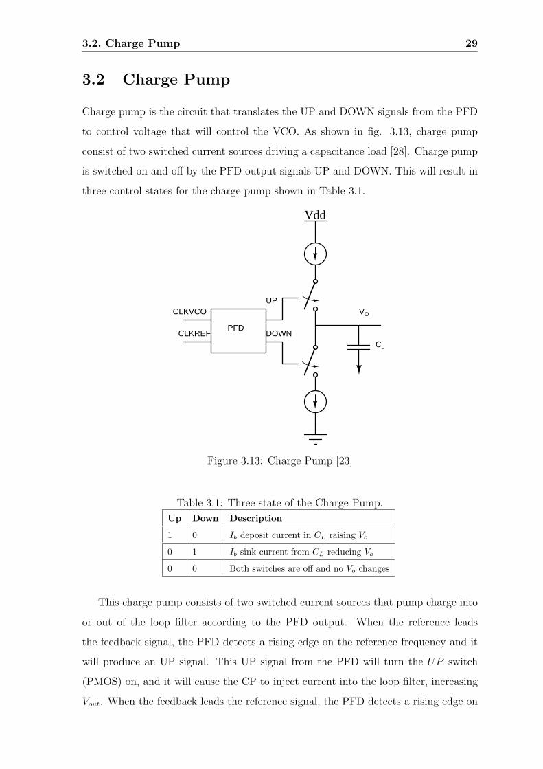
Charge pump is the circuit that translates the UP and DOWN signals from the PFD
to control voltage that will control the VCO. As shown in fig. 3.13, charge pump
consist of two switched current sources driving a capacitance load [28]. Charge pump
is switched on and off by the PFD output signals UP and DOWN. This will result in
three control states for the charge pump shown in Table 3.1.
Vdd
CLKVCO
CLKREFPFD
UP
DOWN
VO
CL
Figure 3.13: Charge Pump [23]
Table 3.1: Three state of the Charge Pump.
Up Down Description
1 0 Ib deposit current in CL raising Vo
0 1 Ib sink current from CL reducing Vo
0 0 Both switches are off and no Vo changes
This charge pump consists of two switched current sources that pump charge into
or out of the loop filter according to the PFD output. When the reference leads
the feedback signal, the PFD detects a rising edge on the reference frequency and it
will produce an UP signal. This UP signal from the PFD will turn the UP switch
(PMOS) on, and it will cause the CP to inject current into the loop filter, increasing
Vout. When the feedback leads the reference signal, the PFD detects a rising edge on
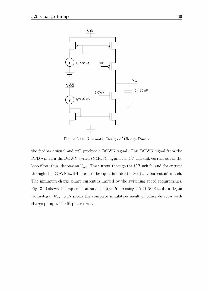
3.2. Charge Pump 30
Vdd
Vdd
Ib=600 uA
Ib=600 uA UP
DOWN
Vout
CL=10 pF
Figure 3.14: Schematic Design of Charge Pump.
the feedback signal and will produce a DOWN signal. This DOWN signal from the
PFD will turn the DOWN switch (NMOS) on, and the CP will sink current out of the
loop filter; thus, decreasing Vout. The current through the UP switch, and the current
through the DOWN switch, need to be equal in order to avoid any current mismatch.
The minimum charge pump current is limited by the switching speed requirements.
Fig. 3.14 shows the implementation of Charge Pump using CADENCE tools in .18µm
technology. Fig. 3.15 shows the complete simulation result of phase detector with
charge pump with 450 phase error.
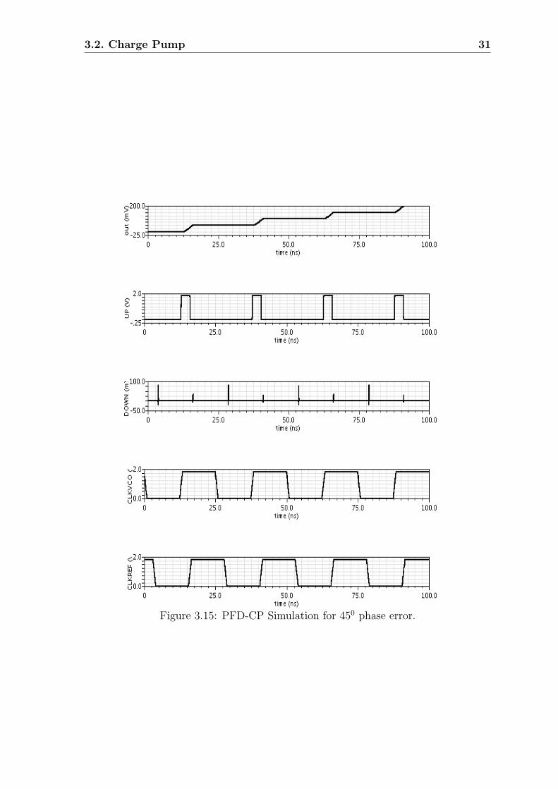
3.2. Charge Pump 31
Figure 3.15: PFD-CP Simulation for 450 phase error.
3.3. True Single Phase Clocked D-Flip Flop (TSPC DFF) 32
3.3 True Single Phase Clocked D-Flip Flop (TSPC
DFF)
D-flip-flops with high-speed operation and low-power consumption are essential for
high performance frequency synthesizers. Various flip-flops have been proposed to
improve the operating speed of dual-modulus pre scalars. The dynamic D-flip-flop de-
signs in previous studies found suffer from glitch and charge-sharing problems [29][30],
which may result in incorrect operations. To alleviate these problems, additional
transistors are introduced to some critical nodes to make these nodes stable [31][32].
However, the newly added transistors limit operating speed and increase power con-
sumption. In high-frequency operations, ratioed logic can replace ratio less logic
without significant penalty on power consumption [33][34]. Ratioed logic, however,
consumes high power in low-frequency operation, and their operating frequency range
is limited.
Dynamic or clocked logic gates are used to decrease circuit complexity, increase
operating speed, and lower power dissipation [35]. Of various dynamic CMOS circuit
techniques, a true single-phase-clock (TSPC) dynamic CMOS circuit is operated with
one clock signal that is never inverted. Therefore, no clock skew exists except for the
clock delay problems, and even higher clock frequency can be achieved [36].
Vdd
MN1
MP1
MPS1CLK
CLK CLK
Y1
N1Y2
N2N3
Qb
MNS1 MNS2
MN2 MN3
MP2 MP3
D
CLK
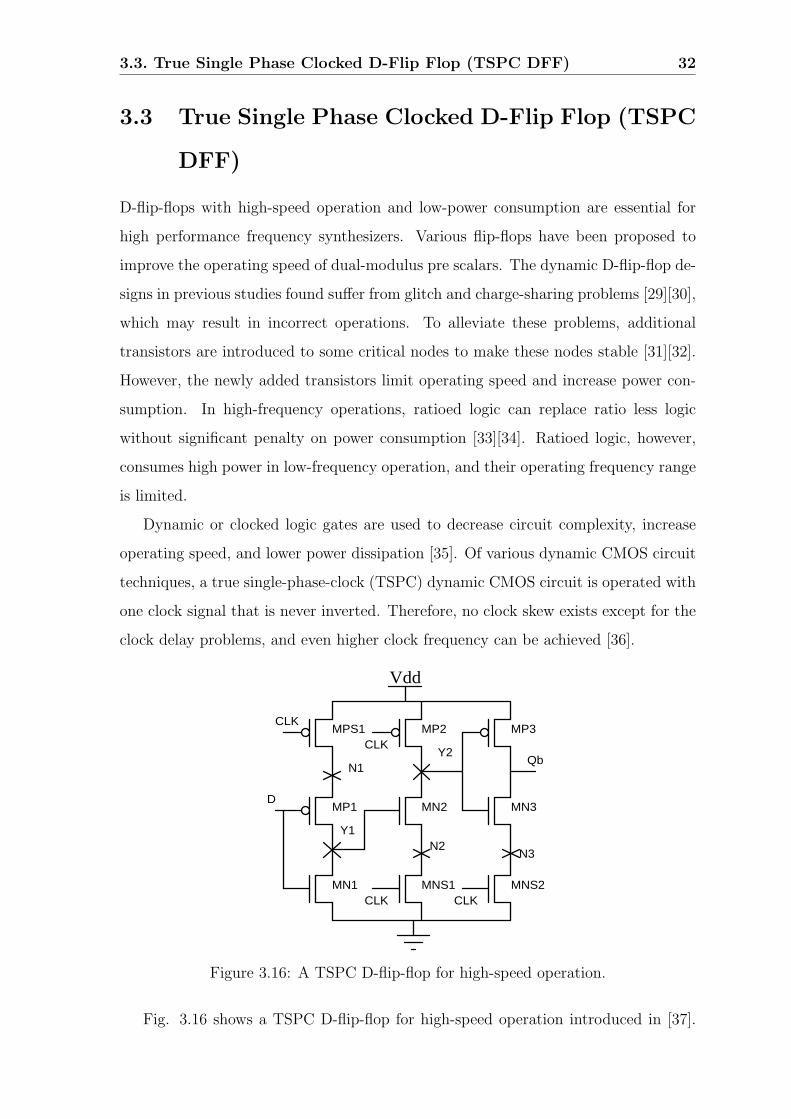
Figure 3.16: A TSPC D-flip-flop for high-speed operation.
Fig. 3.16 shows a TSPC D-flip-flop for high-speed operation introduced in [37].
3.3. True Single Phase Clocked D-Flip Flop (TSPC DFF) 33
The flip-flop consists of nine transistors, where the clocked switching transistors are
placed closer to power/ground for higher speed [38]. The state transition of the flip-
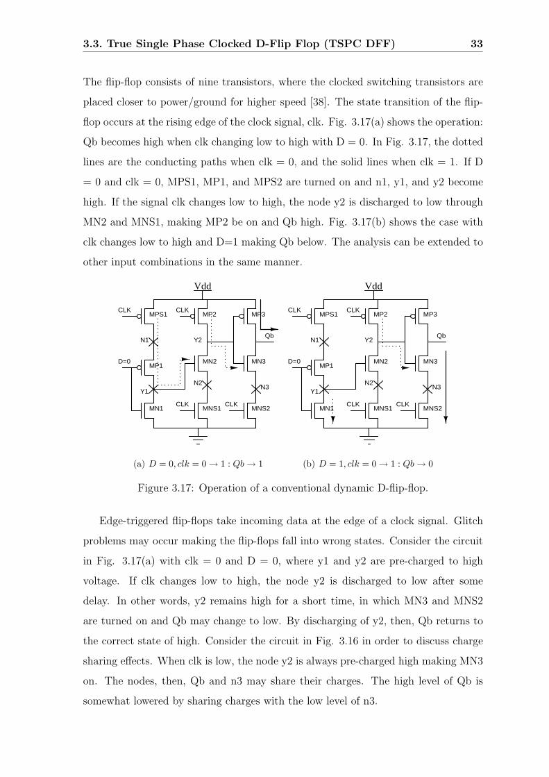
flop occurs at the rising edge of the clock signal, clk. Fig. 3.17(a) shows the operation:
Qb becomes high when clk changing low to high with D = 0. In Fig. 3.17, the dotted
lines are the conducting paths when clk = 0, and the solid lines when clk = 1. If D
= 0 and clk = 0, MPS1, MP1, and MPS2 are turned on and n1, y1, and y2 become
high. If the signal clk changes low to high, the node y2 is discharged to low through
MN2 and MNS1, making MP2 be on and Qb high. Fig. 3.17(b) shows the case with
clk changes low to high and D=1 making Qb below. The analysis can be extended to
other input combinations in the same manner.
Vdd
CLK
D=0
MPS1
MP1
MN1 MNS1CLK
N2Y1
N1 Y2
MN2
MP2 MP3
MN3
MNS2
N3
Qb
CLK
CLK
(a) D = 0, clk = 0→ 1 : Qb→ 1
Vdd
CLK
D=0
MPS1
MP1
MN1 MNS1CLK
N2Y1
N1 Y2
MN2
MP2 MP3
MN3
MNS2
N3
Qb
CLK
CLK
(b) D = 1, clk = 0→ 1 : Qb→ 0
Figure 3.17: Operation of a conventional dynamic D-flip-flop.
Edge-triggered flip-flops take incoming data at the edge of a clock signal. Glitch
problems may occur making the flip-flops fall into wrong states. Consider the circuit
in Fig. 3.17(a) with clk = 0 and D = 0, where y1 and y2 are pre-charged to high
voltage. If clk changes low to high, the node y2 is discharged to low after some
delay. In other words, y2 remains high for a short time, in which MN3 and MNS2
are turned on and Qb may change to low. By discharging of y2, then, Qb returns to
the correct state of high. Consider the circuit in Fig. 3.16 in order to discuss charge
sharing effects. When clk is low, the node y2 is always pre-charged high making MN3
on. The nodes, then, Qb and n3 may share their charges. The high level of Qb is
somewhat lowered by sharing charges with the low level of n3.
3.3. True Single Phase Clocked D-Flip Flop (TSPC DFF) 34
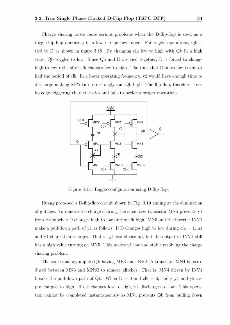
Charge sharing raises more serious problems when the D-flip-flop is used as a
toggle-flip-flop operating in a lower frequency range. For toggle operations, Qb is
tied to D as shown in figure 3.18. By changing clk low to high with Qb in a high
state, Qb toggles to low. Since Qb and D are tied together, D is forced to change
high to low right after clk changes low to high. The time that D stays low is almost
half the period of clk. In a lower operating frequency, y2 would have enough time to
discharge making MP2 turn on strongly and Qb high. The flip-flop, therefore, loses
its edge-triggering characteristics and fails to perform proper operations.
Vdd
MN1
MP1
MPS1CLK
CLK CLK
Y1
N1Y2
N2N3
Qb
MNS1 MNS2
MN2 MN3
MP2 MP3
D
CLK
Q
Figure 3.18: Toggle configuration using D-flip-flop.
Huang proposed a D-flip-flop circuit shown in Fig. 3.19 aiming at the elimination
of glitches. To remove the charge sharing, the small size transistor MN5 prevents y1
from rising when D changes high to low during clk high. MN5 and the inverter INV1
make a pull-down path of y1 as follows. If D changes high to low during clk = 1, n1
and y1 share their charges. That is, y1 would rise up, but the output of INV1 still
has a high value turning on MN5. This makes y1 low and stable resolving the charge
sharing problem.
The same analogy applies Qb having MP3 and INV2. A transistor MN4 is intro-
duced between MN3 and MNS2 to remove glitches. That is, MN4 driven by INV1
breaks the pull-down path of Qb. When D = 0 and clk = 0, nodes y1 and y2 are
pre-charged to high. If clk changes low to high, y2 discharges to low. This opera-
tion cannot be completed instantaneously as MN4 prevents Qb from pulling down
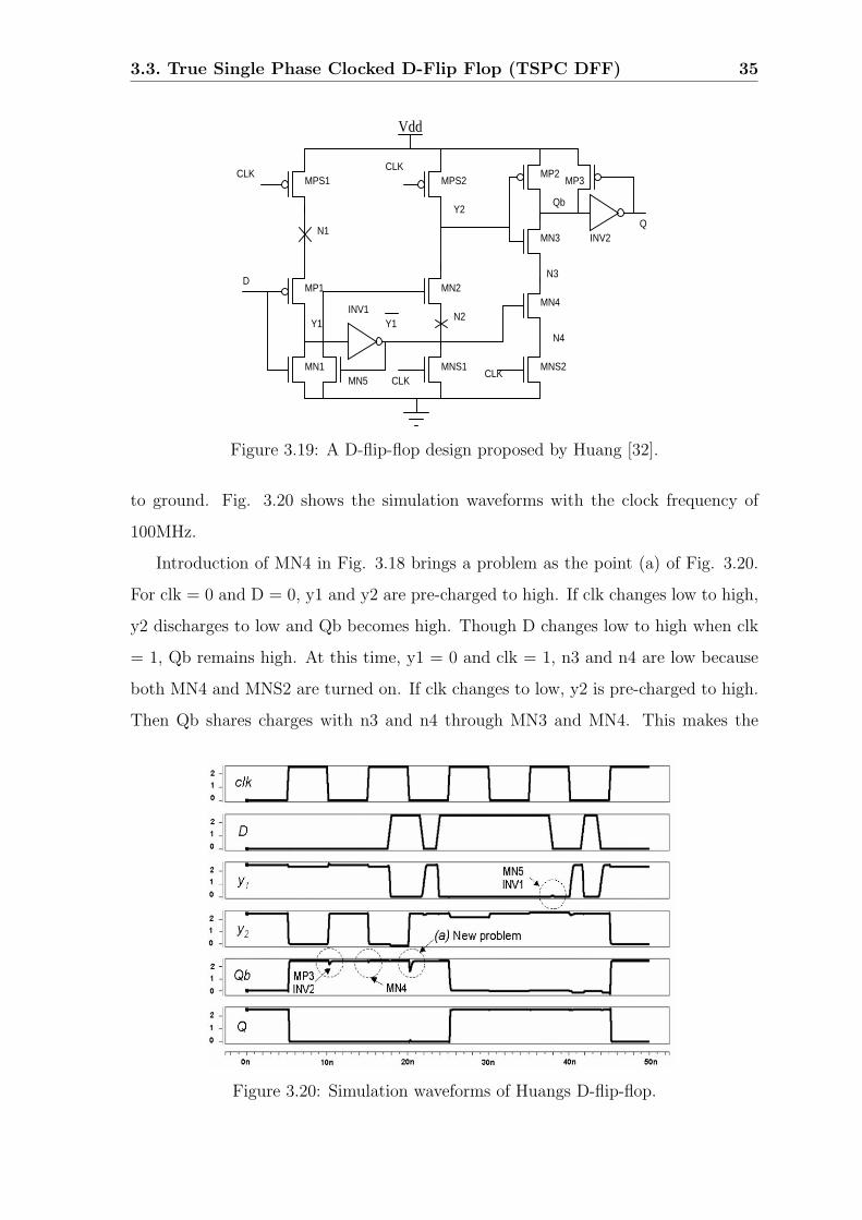
3.3. True Single Phase Clocked D-Flip Flop (TSPC DFF) 35
MP1
MPS1CLK
D
CLK
CLK
INV1
INV2Q
QbY2
Y1
N1
N2
CLK
N3
N4
MNS1
MN2
MPS2MP2
MP3
MN3
MN4
MNS2MN1MN5
Y1
Vdd
Figure 3.19: A D-flip-flop design proposed by Huang [32].
to ground. Fig. 3.20 shows the simulation waveforms with the clock frequency of
100MHz.
Introduction of MN4 in Fig. 3.18 brings a problem as the point (a) of Fig. 3.20.
For clk = 0 and D = 0, y1 and y2 are pre-charged to high. If clk changes low to high,
y2 discharges to low and Qb becomes high. Though D changes low to high when clk
= 1, Qb remains high. At this time, y1 = 0 and clk = 1, n3 and n4 are low because
both MN4 and MNS2 are turned on. If clk changes to low, y2 is pre-charged to high.
Then Qb shares charges with n3 and n4 through MN3 and MN4. This makes the
Figure 3.20: Simulation waveforms of Huangs D-flip-flop.
3.3. True Single Phase Clocked D-Flip Flop (TSPC DFF) 36
voltage of Qb fall down. Even though MP3 can stabilize Qb, the time for returning
to a correct logic value is somewhat long.
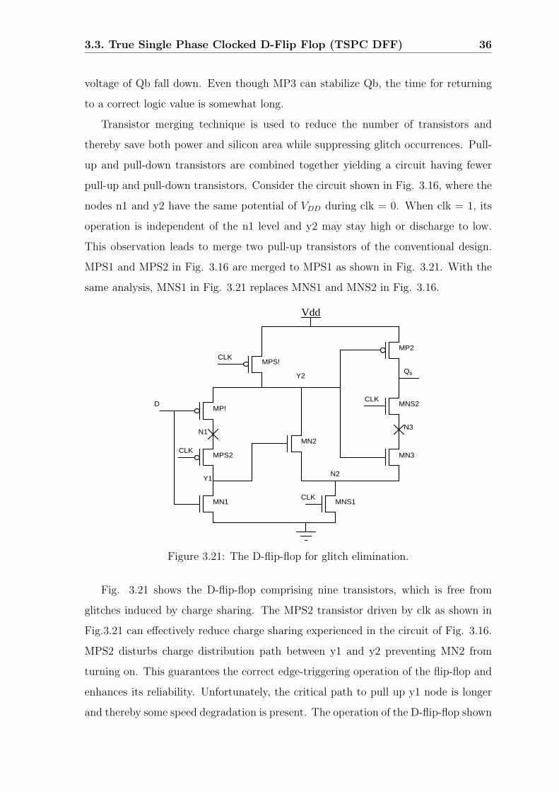
Transistor merging technique is used to reduce the number of transistors and
thereby save both power and silicon area while suppressing glitch occurrences. Pull-
up and pull-down transistors are combined together yielding a circuit having fewer
pull-up and pull-down transistors. Consider the circuit shown in Fig. 3.16, where the
nodes n1 and y2 have the same potential of VDD during clk = 0. When clk = 1, its
operation is independent of the n1 level and y2 may stay high or discharge to low.
This observation leads to merge two pull-up transistors of the conventional design.
MPS1 and MPS2 in Fig. 3.16 are merged to MPS1 as shown in Fig. 3.21. With the
same analysis, MNS1 in Fig. 3.21 replaces MNS1 and MNS2 in Fig. 3.16.
Vdd
D
CLKMPS!
MP!
MPS2
MN1
Y1
MN2
MNS1
N2
MN3
MNS2
MP2
CLK
CLK
Y2
CLK
N1N3
Qb
Figure 3.21: The D-flip-flop for glitch elimination.
Fig. 3.21 shows the D-flip-flop comprising nine transistors, which is free from
glitches induced by charge sharing. The MPS2 transistor driven by clk as shown in
Fig.3.21 can effectively reduce charge sharing experienced in the circuit of Fig. 3.16.
MPS2 disturbs charge distribution path between y1 and y2 preventing MN2 from
turning on. This guarantees the correct edge-triggering operation of the flip-flop and
enhances its reliability. Unfortunately, the critical path to pull up y1 node is longer
and thereby some speed degradation is present. The operation of the D-flip-flop shown
3.3. True Single Phase Clocked D-Flip Flop (TSPC DFF) 37
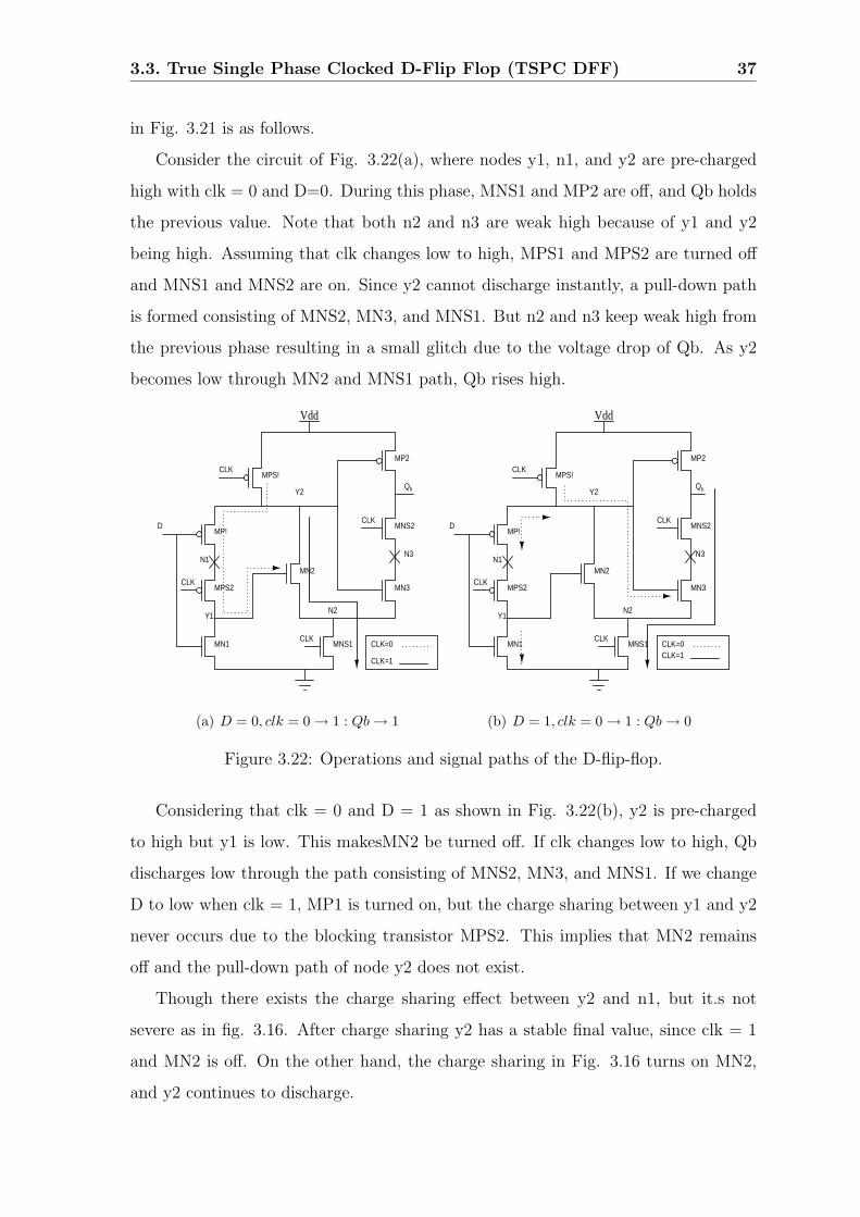
in Fig. 3.21 is as follows.
Consider the circuit of Fig. 3.22(a), where nodes y1, n1, and y2 are pre-charged
high with clk = 0 and D=0. During this phase, MNS1 and MP2 are off, and Qb holds
the previous value. Note that both n2 and n3 are weak high because of y1 and y2
being high. Assuming that clk changes low to high, MPS1 and MPS2 are turned off
and MNS1 and MNS2 are on. Since y2 cannot discharge instantly, a pull-down path
is formed consisting of MNS2, MN3, and MNS1. But n2 and n3 keep weak high from
the previous phase resulting in a small glitch due to the voltage drop of Qb. As y2
becomes low through MN2 and MNS1 path, Qb rises high.
Vdd
D
CLKMPS!
MP!
MPS2
MN1
Y1
MN2
MNS1
N2
MN3
MNS2
MP2
CLK
CLK
Y2
CLK
N1
CLK=0
CLK=1
N3
Qb
(a) D = 0, clk = 0→ 1 : Qb→ 1
Vdd
D
CLKMPS!
MP!
MPS2
MN1
Y1
MN2
MNS1
N2
MN3
MNS2
MP2
CLK
CLK
Y2
CLK
N1
CLK=0 CLK=1
N3
Qb
(b) D = 1, clk = 0→ 1 : Qb→ 0
Figure 3.22: Operations and signal paths of the D-flip-flop.
Considering that clk = 0 and D = 1 as shown in Fig. 3.22(b), y2 is pre-charged
to high but y1 is low. This makesMN2 be turned off. If clk changes low to high, Qb
discharges low through the path consisting of MNS2, MN3, and MNS1. If we change
D to low when clk = 1, MP1 is turned on, but the charge sharing between y1 and y2
never occurs due to the blocking transistor MPS2. This implies that MN2 remains
off and the pull-down path of node y2 does not exist.
Though there exists the charge sharing effect between y2 and n1, but it.s not
severe as in fig. 3.16. After charge sharing y2 has a stable final value, since clk = 1
and MN2 is off. On the other hand, the charge sharing in Fig. 3.16 turns on MN2,
and y2 continues to discharge.
3.4. Dual Modulus Pre-scalar 38
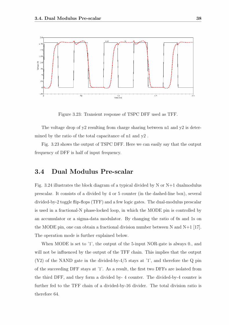
Figure 3.23: Transient response of TSPC DFF used as TFF.
The voltage drop of y2 resulting from charge sharing between n1 and y2 is deter-
mined by the ratio of the total capacitance of n1 and y2 .
Fig. 3.23 shows the output of TSPC DFF. Here we can easily say that the output
frequency of DFF is half of input frequency.
3.4 Dual Modulus Pre-scalar
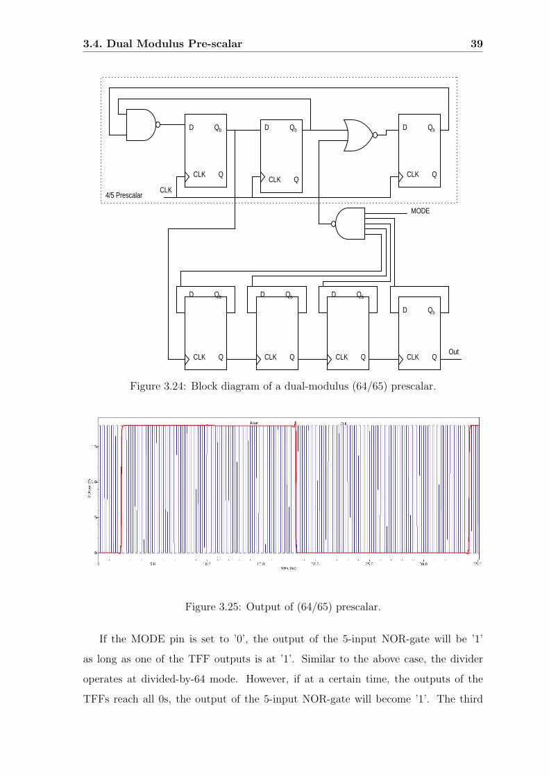
Fig. 3.24 illustrates the block diagram of a typical divided by N or N+1 dualmodulus
prescalar. It consists of a divided by 4 or 5 counter (in the dashed-line box), several
divided-by-2 toggle flip-flops (TFF) and a few logic gates. The dual-modulus prescalar
is used in a fractional-N phase-locked loop, in which the MODE pin is controlled by
an accumulator or a sigma-data modulator. By changing the ratio of 0s and 1s on
the MODE pin, one can obtain a fractional division number between N and N+1 [17].
The operation mode is further explained below.
When MODE is set to ’1’, the output of the 5-input NOR-gate is always 0., and
will not be influenced by the output of the TFF chain. This implies that the output
(Y2) of the NAND gate in the divided-by-4/5 stays at ’1’, and therefore the Q pin
of the succeeding DFF stays at ’1’. As a result, the first two DFFs are isolated from
the third DFF, and they form a divided by- 4 counter. The divided-by-4 counter is
further fed to the TFF chain of a divided-by-16 divider. The total division ratio is
therefore 64.
3.4. Dual Modulus Pre-scalar 39
CLK
CLKCLK
CLK
CLKCLKCLKCLK
Qb Qb Qb
Qb
QbQbQb
D D D
D
DDD
Q
QQQQOut
MODE
4/5 Prescalar
Figure 3.24: Block diagram of a dual-modulus (64/65) prescalar.
Figure 3.25: Output of (64/65) prescalar.
If the MODE pin is set to ’0’, the output of the 5-input NOR-gate will be ’1’
as long as one of the TFF outputs is at ’1’. Similar to the above case, the divider
operates at divided-by-64 mode. However, if at a certain time, the outputs of the
TFFs reach all 0s, the output of the 5-input NOR-gate will become ’1’. The third
3.4. Dual Modulus Pre-scalar 40
DFF in the dashed-line box now comes into operation, and the divided-by-4/5 counter
is in a divided-by-5 configuration. This configuration will delay the transition of Q4
for one input clock cycle (as if one input clock cycle is missing). At the next input
clock cycle, Q4 takes the transition, which drives the TFFs to a non-zero state, and
the divider is put in divided-by-64 configuration again. This is to say, the divider will
repeat its operation per 65 input clock cycles. Therefore, the division ratio is 65 when
MODE = 0. A fractional division ratio between 64 and 65 is achieved by toggling
MODE between ’1’ and ’0’. at a certain ratio. It may be noted that the flip-flops
inside the divided-by- 4 or 5 counter is the speed bottleneck. The remaining flip flops
operate at frequency four times lower than the input frequency.
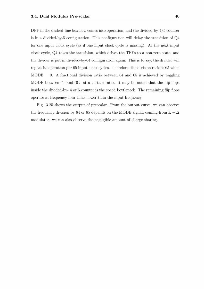
Fig. 3.25 shows the output of prescalar. From the output curve, we can observe
the frequency division by 64 or 65 depends on the MODE signal, coming from Σ−∆
modulator. we can also observe the negligible amount of charge sharing.
Chapter 4
Designing Voltage Controlled
Oscillator
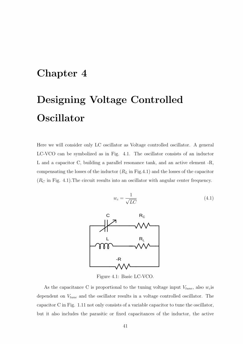
Here we will consider only LC oscillator as Voltage controlled oscillator. A general
LC-VCO can be symbolized as in Fig. 4.1. The oscillator consists of an inductor
L and a capacitor C, building a parallel resonance tank, and an active element -R,
compensating the losses of the inductor (RL in Fig.4.1) and the losses of the capacitor
(RC in Fig. 4.1).The circuit results into an oscillator with angular center frequency.
wc =1√LC
(4.1)
C
L
RC
RL
-R
Figure 4.1: Basic LC-VCO.
As the capacitance C is proportional to the tuning voltage input Vtune, also wcis
dependent on Vtune and the oscillator results in a voltage controlled oscillator. The
capacitor C in Fig. 1.11 not only consists of a variable capacitor to tune the oscillator,
but it also includes the parasitic or fixed capacitances of the inductor, the active
41
42
elements, and of any load connected to the VCO (output driver, mixer, prescalar,
etc.).
Many circuits options to provide the negative resistance of Fig. 4.1, to com-
pensate for the tank losses, are available. Aiming at standard CMOS realizations,
NMOS, PMOS, or a combination of NMOS- and PMOS-transistors can be used.
VCO-structures based on NMOS are presented in Fig. 4.2 [39]. The structure with
the current source to ground has the smallest sensitivity to noise on the ground line,
but the highest sensitivity to the power supply (pushing). This structure has a lower
flicker noise up-conversion than the structure with current source to the supply, due
to the more symmetrical waveforms. This due to the smaller harmonic distortion
caused in a MOS differential pair, if the tail node is connected to a current source
instead of short-circuited to ground. Due to the inductors to the supply voltage,
both structures easily have a signal swing of up to twice the power supply voltage on
each node, which is a very nice feature for phase noise minimization through signal
maximization, but it must be checked very carefully, as the high signal swing will
cause severe MOS-degradation like hot electron effects or even gate oxide breakdown.
Both structures are well suited for low voltage operation, e.g., operation from one
single battery. Similarly, the same VCO-structures can be drawn using PMOS tran-
sistors, and the same discussion as for NMOS can be repeated. PMOS transistors
are about half as fast as NMOS transistors and for the same transconductance per
current, approximately double width is needed. Their lower flicker noise, however, or
the fact that PMOS-transistors are situated in the wells, as most actual processes are
of N-well/p-substrate type, can be a strong argument to use PMOS instead of NMOS.
Finally, both transistor types [40] can be combined to the structures presented in Fig.
4.3.
The combination of NMOS and PMOS transistors generates a negative resistance
from NMOS and PMOS, thus enabling effectively to half the power consumption for
the same negative resistance. The signal swing is limited to power supply voltage,
granting a reliable longtime operation within the voltage limits of the technology.
The choice, whether to put the current source to ground or to power supply, will
be dominated by the primary concern to minimize the sensitivity to ground or to
power supply, which finally will depend on the package, the number of pads, and the
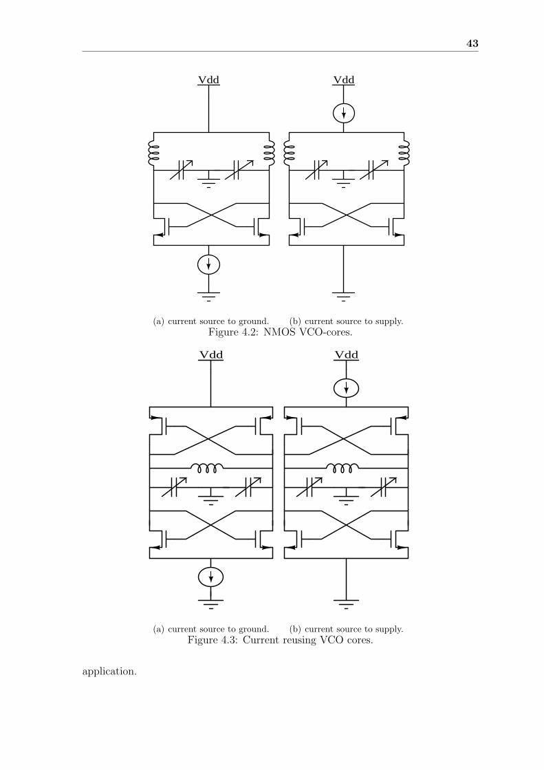
43
Vdd
(a) current source to ground.
Vdd
(b) current source to supply.Figure 4.2: NMOS VCO-cores.
Vdd
(a) current source to ground.
Vdd
(b) current source to supply.Figure 4.3: Current reusing VCO cores.
application.
4.1. Inductor 44
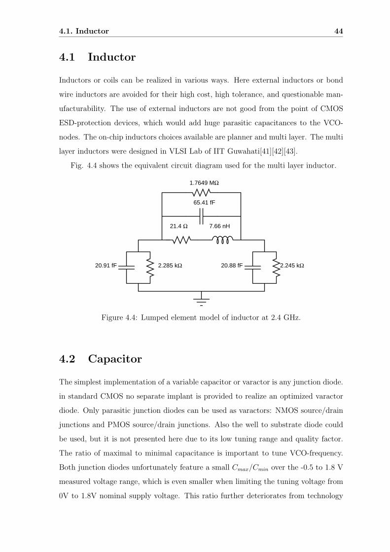
4.1 Inductor
Inductors or coils can be realized in various ways. Here external inductors or bond
wire inductors are avoided for their high cost, high tolerance, and questionable man-
ufacturability. The use of external inductors are not good from the point of CMOS
ESD-protection devices, which would add huge parasitic capacitances to the VCO-
nodes. The on-chip inductors choices available are planner and multi layer. The multi
layer inductors were designed in VLSI Lab of IIT Guwahati[41][42][43].
Fig. 4.4 shows the equivalent circuit diagram used for the multi layer inductor.
20.91 fF 2.285 kΩ 2.245 kΩ20.88 fF
21.4 Ω 7.66 nH
65.41 fF
1.7649 MΩ
Figure 4.4: Lumped element model of inductor at 2.4 GHz.
4.2 Capacitor
The simplest implementation of a variable capacitor or varactor is any junction diode.
in standard CMOS no separate implant is provided to realize an optimized varactor
diode. Only parasitic junction diodes can be used as varactors: NMOS source/drain
junctions and PMOS source/drain junctions. Also the well to substrate diode could
be used, but it is not presented here due to its low tuning range and quality factor.
The ratio of maximal to minimal capacitance is important to tune VCO-frequency.
Both junction diodes unfortunately feature a small Cmax/Cmin over the -0.5 to 1.8 V
measured voltage range, which is even smaller when limiting the tuning voltage from
0V to 1.8V nominal supply voltage. This ratio further deteriorates from technology
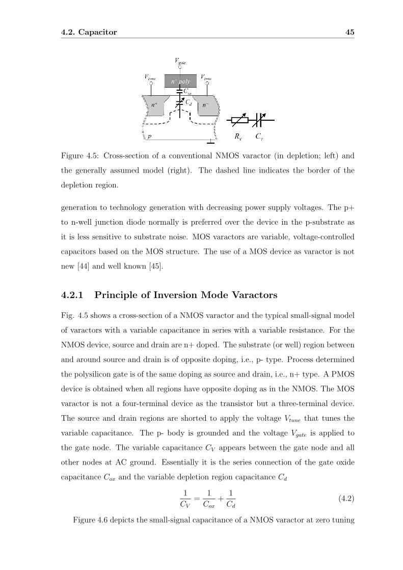
4.2. Capacitor 45
Figure 4.5: Cross-section of a conventional NMOS varactor (in depletion; left) and
the generally assumed model (right). The dashed line indicates the border of the
depletion region.
generation to technology generation with decreasing power supply voltages. The p+
to n-well junction diode normally is preferred over the device in the p-substrate as
it is less sensitive to substrate noise. MOS varactors are variable, voltage-controlled
capacitors based on the MOS structure. The use of a MOS device as varactor is not
new [44] and well known [45].
4.2.1 Principle of Inversion Mode Varactors
Fig. 4.5 shows a cross-section of a NMOS varactor and the typical small-signal model
of varactors with a variable capacitance in series with a variable resistance. For the
NMOS device, source and drain are n+ doped. The substrate (or well) region between
and around source and drain is of opposite doping, i.e., p- type. Process determined
the polysilicon gate is of the same doping as source and drain, i.e., n+ type. A PMOS
device is obtained when all regions have opposite doping as in the NMOS. The MOS
varactor is not a four-terminal device as the transistor but a three-terminal device.
The source and drain regions are shorted to apply the voltage Vtune that tunes the
variable capacitance. The p- body is grounded and the voltage Vgate is applied to
the gate node. The variable capacitance CV appears between the gate node and all
other nodes at AC ground. Essentially it is the series connection of the gate oxide
capacitance Cox and the variable depletion region capacitance Cd
1
CV
=1
Cox
+1
Cd
(4.2)
Figure 4.6 depicts the small-signal capacitance of a NMOS varactor at zero tuning
4.2. Capacitor 46
voltage. The corresponding charges and the relevant lumped elements in the device
are included also. Negative gate voltages result in a hole surplus at the surface of the
semiconductor; the device is in accumulation. Charge variations at the gate are bal-
anced by changes in the accumulation layer charge. A large capacitance determined
by the gate oxide is effective. At increasing gate voltage the flat-band situation is
reached. The semiconductor beneath the gate is neutral and fixed oxide and interface
charges balance the gate charge. The flat-band voltage VFB is usually negative as
especially the oxide charges are comprised of positively charged alkali-ions uninten-
tionally introduced during processing. Further, for the value of VFB the different work
functions of the gate and the well have to be considered. If gate and well are of the
same type of doping flat-band occurs close to 0 V. Different gate and well doping
typically results in VFB close to 1V.
With voltages just above the flat-band voltage, holes are repelled from the surface
and the negatively charged ions of the fixed dopant atoms (acceptors) form a depletion
region. Changes in the gate charge are balanced by more or less negative dopants,
i.e., by a wider or shallower depletion region. The capacitance in this situation is a
series connection of the gate oxide capacitance Cox and the variable depletion region
capacitance Cd.
Gate voltages above a certain threshold Vth result in a surplus of electrons at the
semiconductor surface; the device is in inversion. In this situation the depth of the
depletion region remains constant and changes in the gate charge are balanced by
changes in the electron inversion layer. Again the effective capacitance is determined
by the gate oxide capacitance. The necessary electrons can be provided by thermal
generation in the depletion region. However, at the voltages leading to inversion
the electric field between the gate and the source/drain lowers the barrier between
the source/drain and the semiconductor.s surface considerably. Therefore, the main
source of electrons are the n+ doped source and drain regions.
For highest tank L/C ratio a MOS-varactor with a high Cmax/Cmin is clearly
preferred, as it enables the use of higher inductance values. For maximal varactor
Q a minimal gate length should be preferred, but again MOS-varactor length should
be chosen higher to increase Cmax/Cmin. The MOS-varactors, however, have a very
steep capacitance over voltage characteristic as shown in fig.4.6.
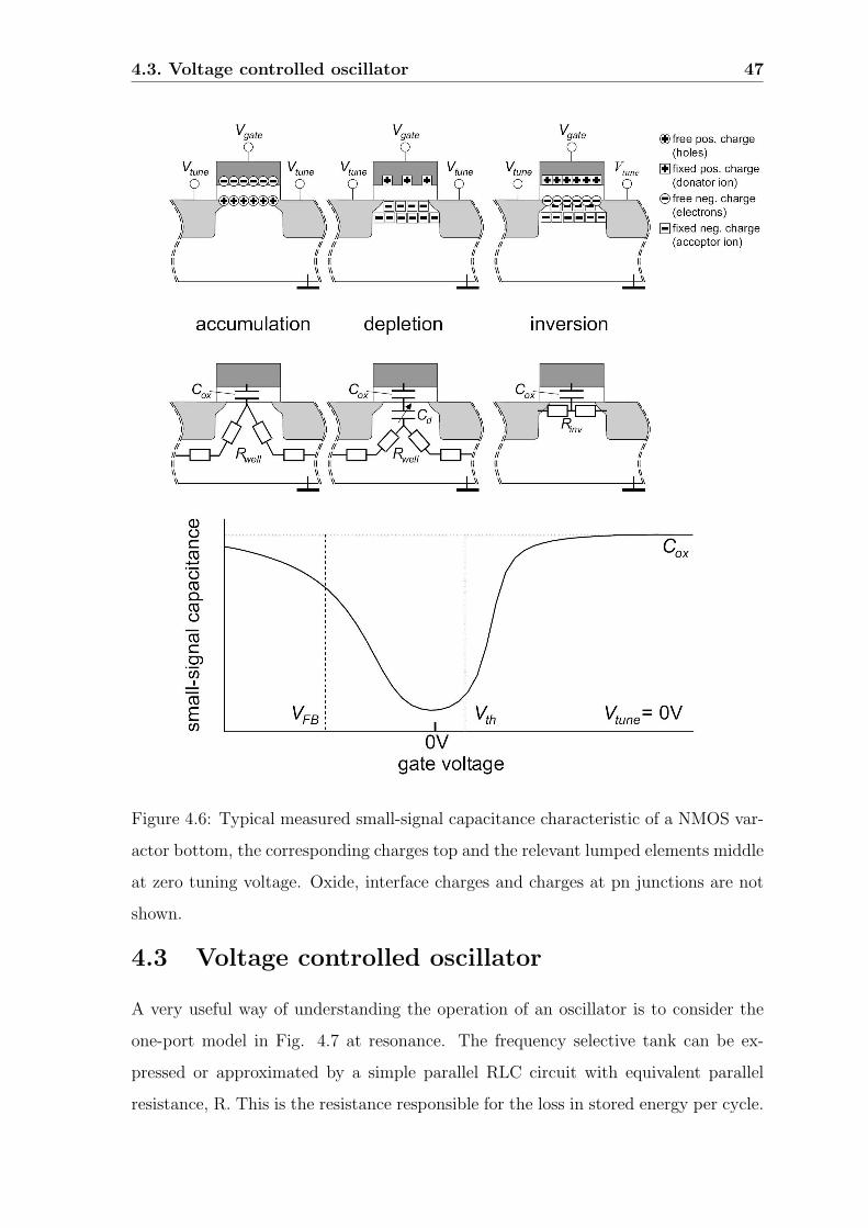
4.3. Voltage controlled oscillator 47
Figure 4.6: Typical measured small-signal capacitance characteristic of a NMOS var-
actor bottom, the corresponding charges top and the relevant lumped elements middle
at zero tuning voltage. Oxide, interface charges and charges at pn junctions are not
shown.
4.3 Voltage controlled oscillator
A very useful way of understanding the operation of an oscillator is to consider the
one-port model in Fig. 4.7 at resonance. The frequency selective tank can be ex-
pressed or approximated by a simple parallel RLC circuit with equivalent parallel
resistance, R. This is the resistance responsible for the loss in stored energy per cycle.
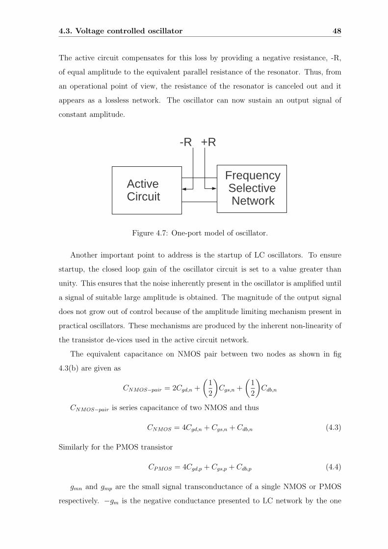
4.3. Voltage controlled oscillator 48
The active circuit compensates for this loss by providing a negative resistance, -R,
of equal amplitude to the equivalent parallel resistance of the resonator. Thus, from
an operational point of view, the resistance of the resonator is canceled out and it
appears as a lossless network. The oscillator can now sustain an output signal of
constant amplitude.
Frequency Selective Network
ActiveCircuit
+R-R
Figure 4.7: One-port model of oscillator.
Another important point to address is the startup of LC oscillators. To ensure
startup, the closed loop gain of the oscillator circuit is set to a value greater than
unity. This ensures that the noise inherently present in the oscillator is amplified until
a signal of suitable large amplitude is obtained. The magnitude of the output signal
does not grow out of control because of the amplitude limiting mechanism present in
practical oscillators. These mechanisms are produced by the inherent non-linearity of
the transistor de-vices used in the active circuit network.
The equivalent capacitance on NMOS pair between two nodes as shown in fig
4.3(b) are given as
CNMOS−pair = 2Cgd,n +
(1
2
)Cgs,n +
(1
2
)Cdb,n
CNMOS−pair is series capacitance of two NMOS and thus
CNMOS = 4Cgd,n + Cgs,n + Cdb,n (4.3)
Similarly for the PMOS transistor
CPMOS = 4Cgd,p + Cgs,p + Cdb,p (4.4)
gmn and gmp are the small signal transconductance of a single NMOS or PMOS
respectively. −gm is the negative conductance presented to LC network by the one
4.3. Voltage controlled oscillator 49
MOS of architecture shown in fig.4.3. gon and gop are the small signal output conduc-
tance of single NMOS and PMOS respectively. All these CNMOS, CPMOS, gon and gop
are small signal quantities in equilibrium, that is when the output differential voltage
across LC tank is zero.
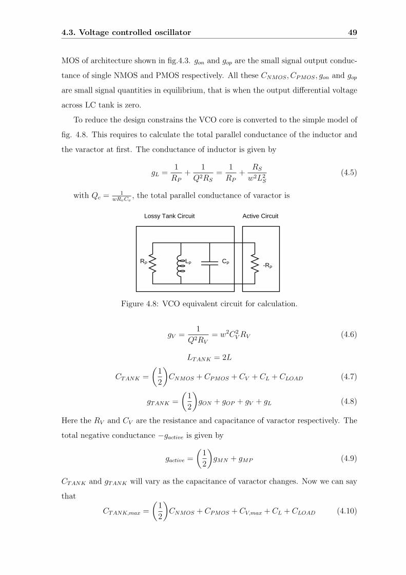
To reduce the design constrains the VCO core is converted to the simple model of
fig. 4.8. This requires to calculate the total parallel conductance of the inductor and
the varactor at first. The conductance of inductor is given by
gL =1
RP
+1
Q2RS
=1
RP
+RS
w2L2S
(4.5)
with Qc = 1wRvCv
, the total parallel conductance of varactor is
-RPRP LP CP
Lossy Tank Circuit Active Circuit
Figure 4.8: VCO equivalent circuit for calculation.
gV =1
Q2RV
= w2C2VRV (4.6)
LTANK = 2L
CTANK =
(1
2
)CNMOS + CPMOS + CV + CL + CLOAD (4.7)
gTANK =
(1
2
)gON + gOP + gV + gL (4.8)
Here the RV and CV are the resistance and capacitance of varactor respectively. The
total negative conductance −gactive is given by
gactive =
(1
2
)gMN + gMP (4.9)
CTANK and gTANK will vary as the capacitance of varactor changes. Now we can say
that
CTANK,max =
(1
2
)CNMOS + CPMOS + CV,max + CL + CLOAD (4.10)
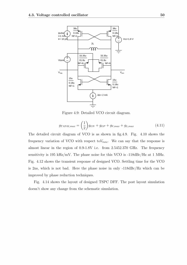
4.3. Voltage controlled oscillator 50
+−
2L
ipulse
idc= 2 mA
Vcc=1.8 V
15u
0.18uNF=1
15u
0.18uNF=1
+−Vtune
38u
0.18u
38u
0.18uNF=1 NF=1i=1 mA
tr= 10 pS
33.35u
01.8u
33.35u
01.8uNF=6NF=6
Vneg Vpos
Figure 4.9: Detailed VCO circuit diagram.
gTANK,max =
(1
2
)gON + gOP + gV,max + gL,max (4.11)
The detailed circuit diagram of VCO is as shown in fig.4.9. Fig. 4.10 shows the
frequency variation of VCO with respect toVtune. We can say that the response is
almost linear in the region of 0.9-1.8V i.e. from 2.5452.370 GHz. The frequency
sensitivity is 195 kHz/mV. The phase noise for this VCO is -118dBc/Hz at 1 MHz.
Fig. 4.12 shows the transient response of designed VCO. Settling time for the VCO
is 2ns, which is not bad. Here the phase noise in only -118dBc/Hz which can be
improved by phase reduction techniques.
Fig. 4.14 shows the layout of designed TSPC DFF. The post layout simulation
doesn’t show any change from the schematic simulation.
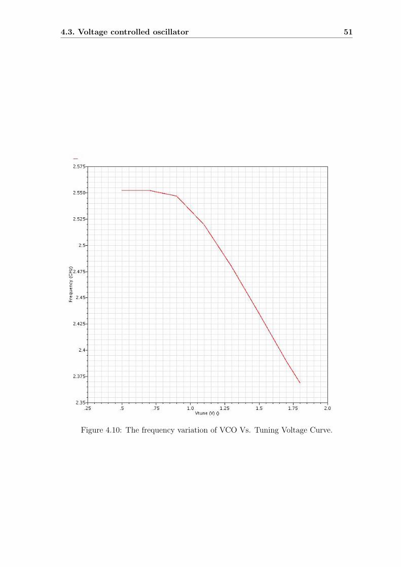
4.3. Voltage controlled oscillator 51
Figure 4.10: The frequency variation of VCO Vs. Tuning Voltage Curve.
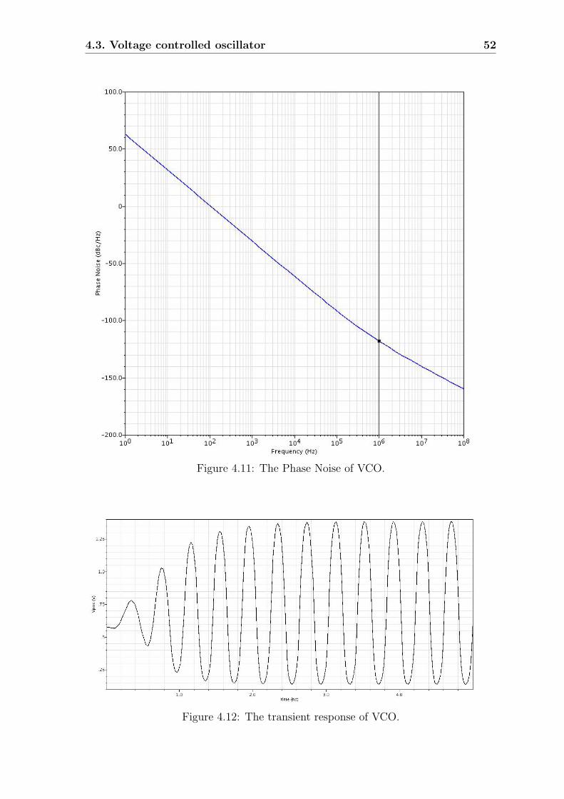
4.3. Voltage controlled oscillator 52
Figure 4.11: The Phase Noise of VCO.
Figure 4.12: The transient response of VCO.
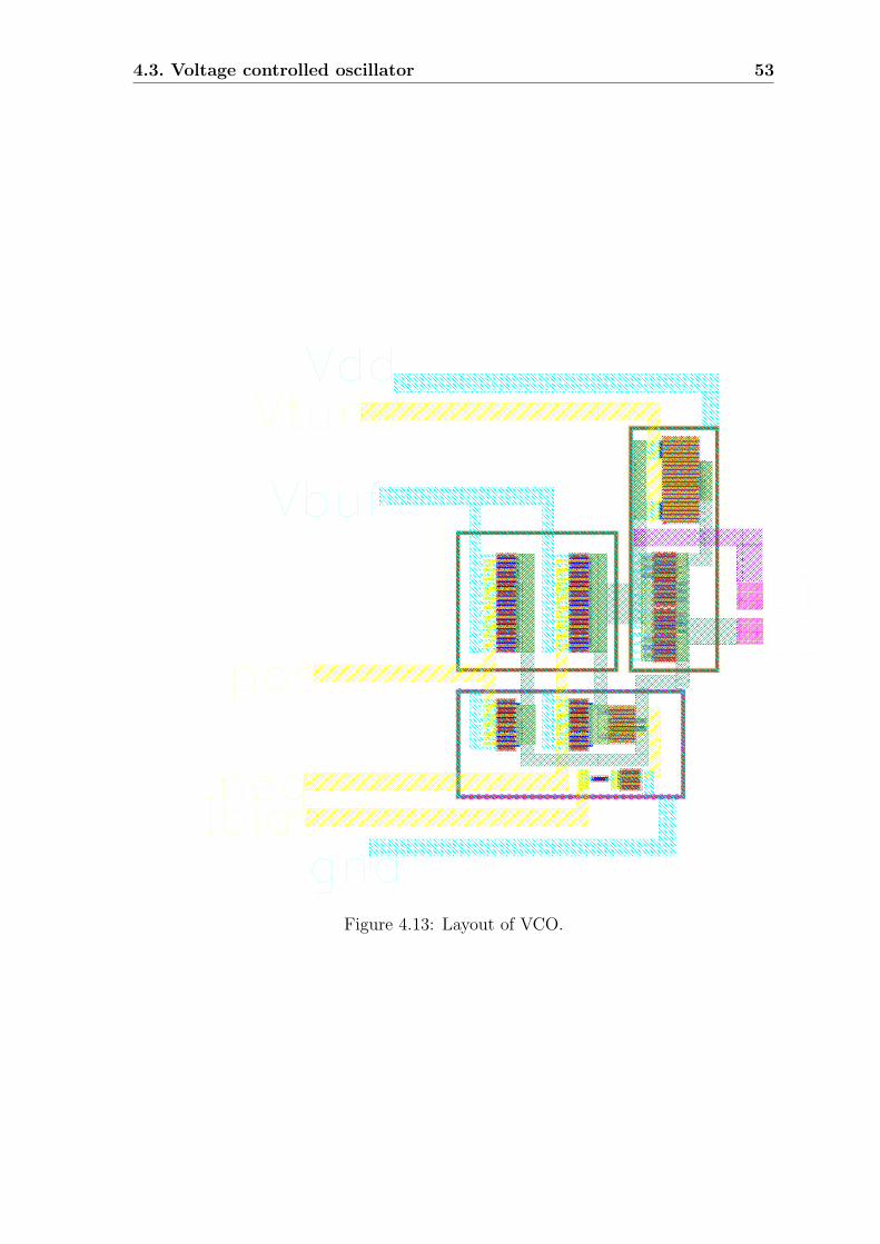
4.3. Voltage controlled oscillator 53
Figure 4.13: Layout of VCO.
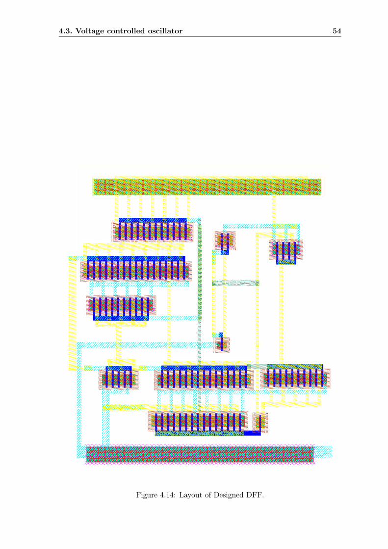
4.3. Voltage controlled oscillator 54
Figure 4.14: Layout of Designed DFF.
Chapter 5
Future work and conclusion
In summary the design of Phase/Frequency Detector, Charge Pump, TSPC DFF,
dual modulus prescalar and VCO has done in thesis work using CADENCE tools.
5.1 Conclusion
This thesis investigate the design steps required to build a Fractional-N Frequency
Synthesizer using PLL. Different architecture of DFF is used to reduce the power
consumption in Phase/Frequency Detector. High speed TSPC DFF has designed to
divide the frequency of GHz range. The design of VCO is carried out in 0.18µm
technology using CADENCE tools. The phase noise can be still reduce after applying
some phase noise reduction techniques. While the phase noise of overall system again
can be reduced by using Σ − ∆ Modulator in feedback loop. The Phase/Frequency
Detector of first type has power dissipation of 9.81µW at 40 MHz and the dead zone of
40 ps. While the type 2 Phase/Frequency Detector have power dissipation of 6.228µW
at 40 MHz and the dead zone of 15 ps which is equal to 0.0012π. the phase noise of
VCO is -118 dBc/Hz at 1 MHz.
5.2 Future work
There is a good scope in this direction. The Fractional-N Frequency Synthesizer has
to be tapped out with the work on Σ−∆ Modulator, which will give the good phase
noise of overall system. The different type of phase noise reduction techniques can
55
5.2. Future work 56
also be employed to reduce the phase noise.
References
[1] European Broadcasting Union, “Digital Video Broadcasting (DVB);DVB-SH im-
plementation guidelines,” pp. 27–29, Dec. 2008.
[2] W. Rhee, “Design of high-performance CMOS charge pumps in phase locked
loops,” IEEE Proceedings of ISCAS, vol. 2, pp. 545–548, June 1999.
[3] D. Byrd and C. Davis, “A fast locking scheme for PLL frequency synthesizers,”
Aplication Notes, National Semiconductor Corporation, July 1995.
[4] B. Memmler, E. Gotz, and G. Schonleber, “New fast-lock PLL for mobile GSM
GPRS application,” Proc. European Solid-State Circuits Conference, pp. 468–
471, Sept. 2000.
[5] G. C. Gillette, “The digiphase synthesizer,” Proceedings of 23rd Annual Frequency
Control Symposium, pp. 25–29, April 1969.
[6] J. Gibbs and R. Temple, “Frequency domain yields its data to phase-locked
synthesizer,” Electronics, pp. 107–113, April 1978.
[7] T. A. Riley, M. A. Copeland and T. A. Kwasnieski, “Delta-Sigma modulation in
fractional-n frequency synthesis,” IEEE J. Solid-St. Circ., vol. 28, pp. 553–559,
May 1993.
[8] W. Rhee, B. Song and A. Ali, “A 1.1-GHz CMOS fractional-N frequency synthe-
sizer with a 3-b third-order ∆− Σ modulator,” IEEE J. Solid-St. Circ., vol. 35,
pp. 1453–1460, Oct. 2000.
[9] M. H. Perrot, T. Tewksbury and C. G. Sodini, “A 27-mW CMOS fractional-N
synthesizer using digital compensation for 2.5 Mb/s GFSK modulation,” IEEE
J. Solid-St. Circ., vol. 32, pp. 2048–2060, Dec. 1997.
57
REFERENCES 58
[10] B. De Muer and M. Steyaert, “A CMOS monolithic ∆Σ-controlled fractional-N
frequency synthesizer or DCS-1800,” IEEE J. Solid-St. Circ., vol. 37, pp. 835–
844, July 2002.
[11] C. Heng and B. Song, “A 1.8-GHz CMOS fractional-N frequency synthesizer with
randomized multiphase VCO,” IEEE J. Solid-St. Circ., vol. 38, pp. 848–854, June
2003.
[12] D. G. Wilson, W. Rhee, and B. S. Song, Integrated RF receiver front ends and fre-
quency synthesizers for wireless. Designing Low Power Digital Systems, Emerging
Technologies, IEEE Press, New York, 1996.
[13] Dana Series 7000 Digiphase Frequency Synthesizers. Dana Laboratories, Inc,
Publication 980428, 1973.
[14] W. Djen, “SA8025 fractional-N synthesizer for 2 GHz band applications,” Appli-
cation Note, Philips Semiconductors, Sept. 1994.
[15] V. Reinhardt, “Spur reduction techniques in direct digital synthesizers,” Pro-
ceedings of 47th Frequency Control Symposium, pp. 230–241, Oct. 1993.
[16] T. A. Riley, M. Copeland, and T. Kwasniewski, “Delta-Sigma modulation in
fractional-N frequency synthesis,” IEEE Journal of Solid-State Circuits, vol. 28,
pp. 553–559, May 1993.
[17] B. Miller and R. Conley, “A multiple modulator fractional divider,” IEEE Trans-
actions on Instrumentation and Measurement, vol. 40, pp. 578–583, June 1991.
[18] N. Filiol, T. Riley, C. Plett, and M. Copeland, “An agile ISM band frequency
synthesizer with built-in GMSK data modulation,” IEEE Journal of Solid-State
Circuits, vol. 33, pp. 998–1008, July 1997.
[19] M. Perrott, T. Tewksbury, and C. Sodini, “A 27 mW CMOS fractional-N synthe-
sizer using digital compensation for 2.5 Mb/s GFSK modulation,” IEEE Journal
of Solid-State Circuits, vol. 32, pp. 2048–2060, Dec. 1997.
[20] T. Weigandt and S. Mehta, “A phase interpolation technique for fractional-N
frequency synthesis,” RF Integrated Circuit Design Group.
REFERENCES 59
[21] W. Rhee, “Design of low-jitter 1 GHz phase-locked loops for digital clock gener-
ation,” IEEE Proceedings of ISCAS , vol. 2, pp. 520–523, May 1999.
[22] W. Rhee and A. Ali, “An on-chip phase-compensation technique in fractional-N
frequency synthesis,” IEEE Proceedings of ISCAS, vol. 3, pp. 363–366, May 1999.
[23] T. Nakagawa and T. Ohira, “A phase noise reduction technique for MMIC fre-
quency synthesizers that uses a new pulse generator LSI,” IEEE Transactions on
Microwave Theory and Technique, vol. 42, pp. 2579–2582, Dec. 1994.
[24] Chou, Chien-Ping, Lin, Zhi-Ming,and Chen, Jun-Da, “A 3-ps dead-zone double-
edge-checking phase-frequency-detector with 4.78 GHz operation frequency,” The
2004 IEEE Asia-Pacific Conference on Circuits and Systems conference, vol. 2,
pp. 937–940, 2004.
[25] Barrett, Curtis, Fractional/ Integer-N PLL Basics. Texas Instruments, Wireless
Communication Business Unit, August 1999.
[26] Won-Hyo Lee, Sung-Dae Lee, and Jun-Dong Cho, “A high-speed, low-power
phase frequency detector and charge pump circuits for high frequency phase
locked loops,” IEICE TRANS. Fundamentals, vol. E82, pp. 2514–2520, 1993.
[27] Chou, Chien-Ping, Lin, Zhi-Ming, and Chen, Jun-Da, “A 3 ps dead-zone double-
edge-checking phase-frequency-detector with 4.78 GH operation frequency,” The
2004 IEEE Asia-Pacific Conference on Circuits and Systems conference, vol. 2,
pp. 937–940, 2004.
[28] Juarez-Hernandez and Alejandro Diaz-Sanchez, “A novel CMOS charge-pump
circuit with positive feedback for PLL applications,” The 8th IEEE International
Conference on Electronics, Circuits and Systems, vol. 1, pp. 349–352, 2001.
[29] J. Yuan and C. Svensson, “High-speed CMOS circuit technique,” IEEE Journal
Solid-State Circuits, vol. 24, pp. 62–70, Feb. 1989.
[30] R. Rogenmoser, N. Felber, Q. Huang, and W. Fichtner, “1.16 GHz dual-modulus
1.2 µm CMOS prescaler,” Proc. IEEE 1993 CICC, p. 27.6.127.6.4, May 1993.
REFERENCES 60
[31] Q. Huang and R. Rogenmoser, “A glitch-free single-phase DFF for gigahertz
applications,” Proc. IEEE 1994 ISCAS, vol. 4, pp. 11–13, May 1994.
[32] R. Rogenmoser, Q. Huang, and F. Piaza, “1.57 GHz asynchronous and 1.4 GHz
dual-modulus 1.2 µm CMOS prescaler,” Proc. IEEE 1994 CICC, pp. 387–390,
May 1994.
[33] B. Chang, J. Park, and W. Kim, “A 1.2 GHz CMOS dualmodulus prescaler
using new dynamic D-type flip-flops,” IEEE Journal Solid-State Circuits, vol. 31,
pp. 749–752, May 1996.
[34] C.-Y. Yang, G-.-K. Dehng, J.-M. Hsu, and S.-I. Liu, “New dynamic flip-flops for
high-speed dual-modulus prescaler,” IEEE Journal Solid-State Circuits, vol. 33,
pp. 1568–1571, Oct. 1998.
[35] R.J. Baker, H.W. Li, and D.E. Boyce, CMOS Circuit Design, Layout, and Sim-
ulation. IEEE Press, New York, 1998.
[36] J. Yuan and C. Svensson, “High-speed CMOS circuit technique,” IEEE J. Solid-
State Circuits, vol. 24, pp. 62–70, Feb. 1989.
[37] H. Oguey and E. Vittoz, “CODYMOS frequency dividers achieve low power
consumption and high frequency,” Electron Lett., pp. pp.386–387, Aug. 1973.
[38] Q. Huang and R. Rogenmoser, “Speed optimization of edge triggered CMOS
circuits for gigahertz single-phase clocks,” IEEE J. Solid-State Circuits, vol. 31,
pp. 456–465, March 1996.
[39] J. Craninckx, M. Steyaert, “A 1.8 GHz low-phase-noise CMOS VCO using op-
timized hollow spiral inductors,” IEEE Journal Solid-State Circuits, vol. 32,
pp. 736–744, May 1997.
[40] A. Hajimiri, T.H. Lee, Low Noise Oscillators. Kluwer,
Boston/Dordrecht/London, 1999.
[41] Genemala Haobijam and Roy Paily, “Multilevel symmetric spiral inductor with
reduced area and higher self resonating frequency,” Indian Microelectronics So-
ciety (IMS) Conference, Aug. 2007.
REFERENCES 61
[42] Genemala Haobijam and Roy Paily, “Systematic analysis, design and optimiza-
tion of on chip spiral inductor for silicon based RFIC’s,” IEEE INDICON, Delhi,
Sept. 2006.
[43] Genemala Haobijam and Roy Paily, “Multilevel pyramidically wound symmetric
spiral inductor,” 11th IEEE VLSI Design And Test Symposium, Kolkata, Aug.
2007.
[44] “Patent submission mos-varactor,” panasonic, 1982.
[45] A.S. Porret, T. Melly, C.C. Enz, E.A. Vittoz, “Design of high-Q varactors for
low-power wireless,” Applications. IEEE Journal Solid-State Circuits, vol. 35(3),
pp. 337–345, March 2000.
Related Documents