MTH500 TETRA Portable Radio R1:380-400 MHz (PT811F) Detailed Service Manual Part Number: 6802963C70 @6802963C70@ Printed on recycled paper. Environmentally friendly cover and spiral bound. European Publications Department . 68P02963C70-O, Issued: 05.02.

Welcome message from author
This document is posted to help you gain knowledge. Please leave a comment to let me know what you think about it! Share it to your friends and learn new things together.
Transcript

MTH500
TETRA Portable RadioR1:380-400 MHz (PT811F)
Detailed Service Manual
Part Number: 6802963C70
@6802963C70@
Printed on recycled paper. Environmentally friendly cover and spiral bound. European Publications Department .68P02963C70-O, Issued: 05.02.

ii 68P02963C70-O
Scope of this Manual
This manual contains information necessary to identify andtroubleshoot the MTH500 Portable radio at the componentlevel. It also contains information on radio assembling, dis-assembling, and maintenance. Accordingly, information inthis manual is divided into four sections:
• Overview
• Theory of Operation
• Troubleshooting
• Radio Programming
• Maintenance
Manual RevisionsChanges which occur after this manual is printed are described in Manual Revisions. These Manual Revisions provide complete information on changes including pertinent parts listing data.
Related Publications• 68P02963C30-O MTH500 User Guide
• 68P02963C65-O MTH500 Basic Service Manual
• 68P02956C20-F CPS User’s Guide
• IFR-Operational Manual Supplement 46882-324
• IFR-Operational Manual 46882-274T
Computer Software CopyrightsThe Motorola products described in this manual may include copyrighted Motorola computer programs stored in semiconductor memories or other media. Laws in the United States and other countries preserve for Motorola certain exclusive rights for copyrighted computer programs, including the exclusive right to copy or reproduce in any form the copyrighted computer program. Accordingly, any copyrighted Motorola computer programs contained in the Motorola products described in this manual may not be copied or reproduced in any manner without the express written permission of Motorola. Furthermore, the purchase of Motorola products shall not be deemed to grant either directly or by implication, estoppel, or otherwise, any license under the copyrights, patents or patent applications of Motorola, except for the normal non-exclusive royalty free license to use that arises by operation of law in the sale of a product.
TrademarksMOTOROLA and the Stylized M Logo are registered in the U.S.Patent and Trademark Office. All other product or service names are the property of their respective owners.
© Motorola, Inc. 2001
Safety And General InformationImportant Information on Safe and Efficient
OperationRead this Information before Using your
handsetThe information provided in this document supersedes the general safety information contained in service manuals published prior to June 2001. For information regarding handset use in a hazardous atmosphere please refer to the Factory Mutual (FM) Approval Manual Supplement or Instruction Card which is included with handset models that offer this capability.
Radio Frequency (RF) Operational CharacteristicsYour handset contains a radio frequency transmitter to convey the information you wish to send as well as occasional automatic signals used to sustain connection with the wireless network, and a receiver which enables you to receive communication and connection information from the network.
Handset Operation And EME ExposureYour Motorola handset is designed to comply with the following national and international standards and guidelines regarding exposure of human beings to radio frequency electromagnetic energy:
• United States Federal Communications Commission, Code of Federal Regulations; 47 CFR part 2 sub-part J
• American National Standards Institute (ANSI) / Institute of Electrical and Electronic Engineers (IEEE) C95. 1-1992
• Institute of Electrical and Electronic Engineers (IEEE) C95.1-1999 Edition
• National Council on Radiation Protection and Measurements (NCRP) of the United States, Report 86, 1986
• International Commission on Non-Ionizing Radiation Protection (ICNIRP) 1998
• Ministry of Health (Canada) Safety Code 6. Limits of Human Exposure to Radiofrequency Electromagnetic Fields in the Frequency Range from 3 kHz to 300 GHz, 1999
68P02963C70-O iii
• Australian Communications Authority Radiocom-munications (Electromagnetic Radiation – Human Exposure) Standard 1999 (applicable to wireless phones only)
• Anatel, Brasil Regulatory Authority“This equipment is in compliance with the limits of Specific Absorption Rate which refer to the exposal to electric, magnetic and electromagnetic fields adopted by ANATEL.”
To assure optimal handset performance and make sure human exposure to radio frequency electromagnetic energy is within the guidelines set forth in the above standards, always adhere to the following procedures:
Phone OperationWhen placing or receiving a phone call, hold your handset as you would a wireline telephone. Speak directly into the microphone.
Two-way radio OperationWhen using your handset, hold the handset in a vertical position with the microphone 2.5 to 5 cm away from your mouth.
Body-worn OperationTo maintain compliance with these RF exposure guidelines, if you wear a handset on your body when transmitting, always place the handset in a Motorola approved belt clip or leather case for this product. Use of non-Motorola-approved accessories may exceed these RF exposure guidelines. If you do not use a Motorola approved body-worn accessory and are not using the handset in the intended use positions along side of the head in the phone mode or in front of the face in the two-way radio mode, then ensure the antenna and handset is kept the following minimum distances from the body when transmitting:
• Phone or Two-way radio mode: 2.5 cm
• Data operation using any data feature with orwithout an accessory cable: 2.5 cm
Antenna CareUse only the supplied or an approved replacement antenna. Unauthorized antennas, modifications, or attachments could damage the handset and may violate FCC regulations.
DO NOT hold the antenna when the radio is “IN USE”. Holding the antenna affects call quality and may cause the radio to operate at a higher power level than needed.
Approved AccessoriesFor a list of Approved Motorola accessories, please see “REPLACEMENT PARTS AND KITS” on page 45.
Electromagnetic Interference/CompatibilityNOTE: Nearly every electronic device is susceptible to electromagnetic interference (EMI) if inadequately shielded, designed or otherwise configured for electromagnetic compatibility.
FacilitiesTo avoid electromagnetic interference and/or compatibility conflicts, turn off your handset in any facility where posted notices instruct you to do so. Hospitals or health care facilities may be using equipment that is sensitive to external RF energy.
AircraftWhen instructed to do so, turn off your handset when on board an aircraft. Any use of a handset must be in accordance with applicable regulations per airline crew instructions.
Medical Devices
PacemakersThe Health Industry Manufacturers Association recommends that a minimum separation of 15 centimetres be maintained between a handheld wireless handset and a pacemaker. These recommendations are consistent with those of the U.S Food and Drug Administration.Persons with pacemakers should:• ALWAYS keep the handset more than 15 centi-
metres from their pacemaker when the handset is turned ON.
• not carry the handset in the breast pocket.• use the ear opposite the pacemaker to minimise
the potential for interference.• turn the handset OFF immediately if you have
any reason to suspect that interference is taking place.
Hearing AidsSome digital wireless handsets may interfere with some hearing aids. In the event of such interference, you may want to consult your hearing aid manufacturer to discuss alternatives.
Other Medical DevicesIf you use any other personal medical device, consult the manufacturer of your device to determine if it is adequately shielded from RF energy. Your physician may be able to assist you in obtaining this information.

iv 68P02963C70-O
Safety and General
Use While DrivingCheck the laws and regulations on the use of radios in the area where you drive. Always obey them. When using the handset while driving, please:• Give full attention to driving and to the road.• Use hands-free operation, if available.• Pull off the road and park before making or answering a
call if driving conditions so require.
Operational Warnings
For Vehicles Equipped with an Air BagDo Not place a handset or install a Vehicular Adapter in the area over an air bag or in the air bag deployment area. Air bags inflate with great force. If a radio is placed in the air bag deployment area and the air bag inflates, the radio may be propelled with great force and cause serious injury to occupants of the vehicle.
Potentially Explosive AtmospheresTurn off your handset prior to entering any area with a potentially explosive atmosphere, unless it is a handset type especially qualified for use in such areas as “Intrinsically Safe” (for example, Factory Mutual, CSA, UL, or CENELEC Approved). Do not remove, install, or charge batteries in such areas. Sparks in a potentially explosive atmosphere can cause an explosion or fire resulting in bodily injury or even death.NOTE: The areas with potentially explosive atmos-
pheres referred to above include fuelling areas such as below decks on boats, fuel or chemical transfer or storage facilities, areas where the air contains chemicals or particles such as grain, dust, or metal powders, and any other area where you would normally be advised to turn off your vehicle engine. Areas with potentially explosive atmospheres are often, but not always, posted.
Blasting Caps and AreasTo avoid possible interference with blasting operations, turn off your handset when you are near electrical blasting caps, in a blasting area, or in areas posted: “Turn off two-way radio.” Obey all signs and instructions.
!W A R N I N G
!
Operational Cautions
AntennasDo not use any handset that has a damaged antenna. If a damaged antenna comes into contact with your skin, a minor burn can result.
BatteriesAll batteries can cause property damage and/or bodily injury such as burns if a conductive material such as jewellery, keys, or beaded chains touch exposed terminals. The conductive material may complete an electrical circuit (short circuit) and become quite hot. Exercise care in handling any charged battery, particularly when placing it inside a pocket, purse, or other container with metal objects.
European Union Directives Conformance Statement
This product is in conformance with the TETRA (TErrestrial Trunked RAdio) standard.This product is in conformance with the requirements of the applicable EU Council Directives.Declarations of Conformance with the requirements are located at:Motorola a/sMidtager 20DK-2605 Brondby
!C a u t i o n
Contents
68P02963C70-O v
MTH500 Portable Radio Model Information . . . . . . . . . . . . . . . . . . . . . . . . . . . . . . . . . . . . . . . . xi
MTH500 Model Specifications . . . . . . . . . . . . . . . . . . . . . . . . . . . . . . . . . . . . . . . . . . . . . . . . . . . . xii
MTH500 Accessories . . . . . . . . . . . . . . . . . . . . . . . . . . . . . . . . . . . . . . . . . . . . . . . . . . . . . . . . . . . xiii
Overview . . . . . . . . . . . . . . . . . . . . . . . . . . . . . . . . . . . . . . . . . . . . . . . . . . . . . . . . . . . . . . . . . . . . . 1-1General . . . . . . . . . . . . . . . . . . . . . . . . . . . . . . . . . . . . . . . . . . . . . . . . . . . . . . . . . . . . . . . . . . . . . . . . . . . . . . . . . . . . . . . 1-1
Digital Modulation Technology . . . . . . . . . . . . . . . . . . . . . . . . . . . . . . . . . . . . . . . . . . . . . . . . . . . . . . . . . . . . . . . . . 1-1Voice Compression Technology . . . . . . . . . . . . . . . . . . . . . . . . . . . . . . . . . . . . . . . . . . . . . . . . . . . . . . . . . . . . . . . . . 1-2
Description . . . . . . . . . . . . . . . . . . . . . . . . . . . . . . . . . . . . . . . . . . . . . . . . . . . . . . . . . . . . . . . . . . . . . . . . . . . . . . . . . . . . 1-2Transceiver Description . . . . . . . . . . . . . . . . . . . . . . . . . . . . . . . . . . . . . . . . . . . . . . . . . . . . . . . . . . . . . . . . . . . . . . . 1-2
Digital Section Description . . . . . . . . . . . . . . . . . . . . . . . . . . . . . . . . . . . . . . . . . . . . . . . . . . . . . . . . . . . . . . . . . . 1-2Transmitter Path Description . . . . . . . . . . . . . . . . . . . . . . . . . . . . . . . . . . . . . . . . . . . . . . . . . . . . . . . . . . . . . . . . . 1-2Receiver Path Description . . . . . . . . . . . . . . . . . . . . . . . . . . . . . . . . . . . . . . . . . . . . . . . . . . . . . . . . . . . . . . . . . . . 1-3Frequency Generating Section Description . . . . . . . . . . . . . . . . . . . . . . . . . . . . . . . . . . . . . . . . . . . . . . . . . . . . . . 1-3
Theory of Operation . . . . . . . . . . . . . . . . . . . . . . . . . . . . . . . . . . . . . . . . . . . . . . . . . . . . . . . . . . . 2-1Section Introduction . . . . . . . . . . . . . . . . . . . . . . . . . . . . . . . . . . . . . . . . . . . . . . . . . . . . . . . . . . . . . . . . . . . . . . . . . . . . . 2-1
Block Diagram Overview . . . . . . . . . . . . . . . . . . . . . . . . . . . . . . . . . . . . . . . . . . . . . . . . . . . . . . . . . . . . . . . . . . . . . . . . . 2-1Receiver Section . . . . . . . . . . . . . . . . . . . . . . . . . . . . . . . . . . . . . . . . . . . . . . . . . . . . . . . . . . . . . . . . . . . . . . . . . . . . . 2-2Transmitter Section . . . . . . . . . . . . . . . . . . . . . . . . . . . . . . . . . . . . . . . . . . . . . . . . . . . . . . . . . . . . . . . . . . . . . . . . . . . 2-3Digital Section . . . . . . . . . . . . . . . . . . . . . . . . . . . . . . . . . . . . . . . . . . . . . . . . . . . . . . . . . . . . . . . . . . . . . . . . . . . . . . . 2-3Frequency Generating Section . . . . . . . . . . . . . . . . . . . . . . . . . . . . . . . . . . . . . . . . . . . . . . . . . . . . . . . . . . . . . . . . . . 2-4
Block Diagrams Descriptions . . . . . . . . . . . . . . . . . . . . . . . . . . . . . . . . . . . . . . . . . . . . . . . . . . . . . . . . . . . . . . . . . . . . . . 2-5Receiver Path . . . . . . . . . . . . . . . . . . . . . . . . . . . . . . . . . . . . . . . . . . . . . . . . . . . . . . . . . . . . . . . . . . . . . . . . . . . . . . . . 2-5Transmitter Path . . . . . . . . . . . . . . . . . . . . . . . . . . . . . . . . . . . . . . . . . . . . . . . . . . . . . . . . . . . . . . . . . . . . . . . . . . . . . 2-6Digital Mode of Operation . . . . . . . . . . . . . . . . . . . . . . . . . . . . . . . . . . . . . . . . . . . . . . . . . . . . . . . . . . . . . . . . . . . . . 2-7Frequency Generating Section . . . . . . . . . . . . . . . . . . . . . . . . . . . . . . . . . . . . . . . . . . . . . . . . . . . . . . . . . . . . . . . . . . 2-8
Main Synthesizer . . . . . . . . . . . . . . . . . . . . . . . . . . . . . . . . . . . . . . . . . . . . . . . . . . . . . . . . . . . . . . . . . . . . . . . . . . 2-9RX Second Local Oscillator (LO) . . . . . . . . . . . . . . . . . . . . . . . . . . . . . . . . . . . . . . . . . . . . . . . . . . . . . . . . . . . . . 2-9Offset VCO . . . . . . . . . . . . . . . . . . . . . . . . . . . . . . . . . . . . . . . . . . . . . . . . . . . . . . . . . . . . . . . . . . . . . . . . . . . . . . 2-9
Detailed Circuit Description . . . . . . . . . . . . . . . . . . . . . . . . . . . . . . . . . . . . . . . . . . . . . . . . . . . . . . . . . . . . . . . . . . . . . . 2-10Receiver Path, Detailed Circuit Description . . . . . . . . . . . . . . . . . . . . . . . . . . . . . . . . . . . . . . . . . . . . . . . . . . . . . . . 2-10
Antenna Switch . . . . . . . . . . . . . . . . . . . . . . . . . . . . . . . . . . . . . . . . . . . . . . . . . . . . . . . . . . . . . . . . . . . . . . . . . . 2-10Limiter . . . . . . . . . . . . . . . . . . . . . . . . . . . . . . . . . . . . . . . . . . . . . . . . . . . . . . . . . . . . . . . . . . . . . . . . . . . . . . . . . 2-11Front Filter . . . . . . . . . . . . . . . . . . . . . . . . . . . . . . . . . . . . . . . . . . . . . . . . . . . . . . . . . . . . . . . . . . . . . . . . . . . . . . 2-11LNA . . . . . . . . . . . . . . . . . . . . . . . . . . . . . . . . . . . . . . . . . . . . . . . . . . . . . . . . . . . . . . . . . . . . . . . . . . . . . . . . . . . 2-11Second Pre-selector . . . . . . . . . . . . . . . . . . . . . . . . . . . . . . . . . . . . . . . . . . . . . . . . . . . . . . . . . . . . . . . . . . . . . . . 2-11Attenuator . . . . . . . . . . . . . . . . . . . . . . . . . . . . . . . . . . . . . . . . . . . . . . . . . . . . . . . . . . . . . . . . . . . . . . . . . . . . . . 2-11

Contents
vi 68P02963C70-O
Mixer . . . . . . . . . . . . . . . . . . . . . . . . . . . . . . . . . . . . . . . . . . . . . . . . . . . . . . . . . . . . . . . . . . . . . . . . . . . . . . . . . 2-11IF Filter . . . . . . . . . . . . . . . . . . . . . . . . . . . . . . . . . . . . . . . . . . . . . . . . . . . . . . . . . . . . . . . . . . . . . . . . . . . . . . . . 2-12BALUN . . . . . . . . . . . . . . . . . . . . . . . . . . . . . . . . . . . . . . . . . . . . . . . . . . . . . . . . . . . . . . . . . . . . . . . . . . . . . . . 2-12WPIC (receiver section) . . . . . . . . . . . . . . . . . . . . . . . . . . . . . . . . . . . . . . . . . . . . . . . . . . . . . . . . . . . . . . . . . . . 2-12
Transmitter Path, Detailed Circuit Description . . . . . . . . . . . . . . . . . . . . . . . . . . . . . . . . . . . . . . . . . . . . . . . . . . . . . . . 2-13Forward Path . . . . . . . . . . . . . . . . . . . . . . . . . . . . . . . . . . . . . . . . . . . . . . . . . . . . . . . . . . . . . . . . . . . . . . . . . . . . . . 2-13
WPIC . . . . . . . . . . . . . . . . . . . . . . . . . . . . . . . . . . . . . . . . . . . . . . . . . . . . . . . . . . . . . . . . . . . . . . . . . . . . . . . . . 2-13LO LINE-UP . . . . . . . . . . . . . . . . . . . . . . . . . . . . . . . . . . . . . . . . . . . . . . . . . . . . . . . . . . . . . . . . . . . . . . . . . . . 2-14LNODCT . . . . . . . . . . . . . . . . . . . . . . . . . . . . . . . . . . . . . . . . . . . . . . . . . . . . . . . . . . . . . . . . . . . . . . . . . . . . . . 2-14BALUN - FILTER . . . . . . . . . . . . . . . . . . . . . . . . . . . . . . . . . . . . . . . . . . . . . . . . . . . . . . . . . . . . . . . . . . . . . . . 2-14RF Power Amplifier . . . . . . . . . . . . . . . . . . . . . . . . . . . . . . . . . . . . . . . . . . . . . . . . . . . . . . . . . . . . . . . . . . . . . . 2-15Coupler and Feedback Path . . . . . . . . . . . . . . . . . . . . . . . . . . . . . . . . . . . . . . . . . . . . . . . . . . . . . . . . . . . . . . . . 2-15Isolator . . . . . . . . . . . . . . . . . . . . . . . . . . . . . . . . . . . . . . . . . . . . . . . . . . . . . . . . . . . . . . . . . . . . . . . . . . . . . . . . 2-15Antenna Switch . . . . . . . . . . . . . . . . . . . . . . . . . . . . . . . . . . . . . . . . . . . . . . . . . . . . . . . . . . . . . . . . . . . . . . . . . 2-15Harmonic Filter . . . . . . . . . . . . . . . . . . . . . . . . . . . . . . . . . . . . . . . . . . . . . . . . . . . . . . . . . . . . . . . . . . . . . . . . . 2-16
Digital Section, Detailed Circuit Description . . . . . . . . . . . . . . . . . . . . . . . . . . . . . . . . . . . . . . . . . . . . . . . . . . . . . . . . 2-17Host Memories . . . . . . . . . . . . . . . . . . . . . . . . . . . . . . . . . . . . . . . . . . . . . . . . . . . . . . . . . . . . . . . . . . . . . . . . . . . . . 2-17
Flash Memory . . . . . . . . . . . . . . . . . . . . . . . . . . . . . . . . . . . . . . . . . . . . . . . . . . . . . . . . . . . . . . . . . . . . . . . . . . . 2-17SRAM Memory . . . . . . . . . . . . . . . . . . . . . . . . . . . . . . . . . . . . . . . . . . . . . . . . . . . . . . . . . . . . . . . . . . . . . . . . . 2-18
Serial Peripheral Interface (SPI) . . . . . . . . . . . . . . . . . . . . . . . . . . . . . . . . . . . . . . . . . . . . . . . . . . . . . . . . . . . . . . . 2-18DC Power Distribution . . . . . . . . . . . . . . . . . . . . . . . . . . . . . . . . . . . . . . . . . . . . . . . . . . . . . . . . . . . . . . . . . . . . . . . 2-20
V1 Linear Regulator . . . . . . . . . . . . . . . . . . . . . . . . . . . . . . . . . . . . . . . . . . . . . . . . . . . . . . . . . . . . . . . . . . . . . . 2-20V2 Linear Regulator . . . . . . . . . . . . . . . . . . . . . . . . . . . . . . . . . . . . . . . . . . . . . . . . . . . . . . . . . . . . . . . . . . . . . . 2-20V3 Linear Regulator . . . . . . . . . . . . . . . . . . . . . . . . . . . . . . . . . . . . . . . . . . . . . . . . . . . . . . . . . . . . . . . . . . . . . . 2-20V4 Linear Regulator . . . . . . . . . . . . . . . . . . . . . . . . . . . . . . . . . . . . . . . . . . . . . . . . . . . . . . . . . . . . . . . . . . . . . . 2-20Switcher #1 (Synchronous Buck Mode Converter) . . . . . . . . . . . . . . . . . . . . . . . . . . . . . . . . . . . . . . . . . . . . . . 2-20Switcher #2 (Boost Mode Converter) . . . . . . . . . . . . . . . . . . . . . . . . . . . . . . . . . . . . . . . . . . . . . . . . . . . . . . . . . 2-21DSC Linear Regulator . . . . . . . . . . . . . . . . . . . . . . . . . . . . . . . . . . . . . . . . . . . . . . . . . . . . . . . . . . . . . . . . . . . . 2-21TS_REF Linear Regulator . . . . . . . . . . . . . . . . . . . . . . . . . . . . . . . . . . . . . . . . . . . . . . . . . . . . . . . . . . . . . . . . . 2-21VREF1 Linear Regulator . . . . . . . . . . . . . . . . . . . . . . . . . . . . . . . . . . . . . . . . . . . . . . . . . . . . . . . . . . . . . . . . . . 2-21VREF2 Linear Regulator . . . . . . . . . . . . . . . . . . . . . . . . . . . . . . . . . . . . . . . . . . . . . . . . . . . . . . . . . . . . . . . . . . 2-21Current Limit . . . . . . . . . . . . . . . . . . . . . . . . . . . . . . . . . . . . . . . . . . . . . . . . . . . . . . . . . . . . . . . . . . . . . . . . . . . 2-21
RS232, SB9600 . . . . . . . . . . . . . . . . . . . . . . . . . . . . . . . . . . . . . . . . . . . . . . . . . . . . . . . . . . . . . . . . . . . . . . . . . . . . 2-23Battery ID . . . . . . . . . . . . . . . . . . . . . . . . . . . . . . . . . . . . . . . . . . . . . . . . . . . . . . . . . . . . . . . . . . . . . . . . . . . . . . . . . 2-23Radio Audio System . . . . . . . . . . . . . . . . . . . . . . . . . . . . . . . . . . . . . . . . . . . . . . . . . . . . . . . . . . . . . . . . . . . . . . . . . 2-23
Tx Path . . . . . . . . . . . . . . . . . . . . . . . . . . . . . . . . . . . . . . . . . . . . . . . . . . . . . . . . . . . . . . . . . . . . . . . . . . . . . . . . 2-23Rx Path . . . . . . . . . . . . . . . . . . . . . . . . . . . . . . . . . . . . . . . . . . . . . . . . . . . . . . . . . . . . . . . . . . . . . . . . . . . . . . . . 2-23
Frequency Generating Section Detailed Circuit Description . . . . . . . . . . . . . . . . . . . . . . . . . . . . . . . . . . . . . . . . . . . . . 2-25REF. Oscillator - TCXO . . . . . . . . . . . . . . . . . . . . . . . . . . . . . . . . . . . . . . . . . . . . . . . . . . . . . . . . . . . . . . . . . . . . . . 2-26Main VCO and Main Synthesizer . . . . . . . . . . . . . . . . . . . . . . . . . . . . . . . . . . . . . . . . . . . . . . . . . . . . . . . . . . . . . . 2-26WPIC . . . . . . . . . . . . . . . . . . . . . . . . . . . . . . . . . . . . . . . . . . . . . . . . . . . . . . . . . . . . . . . . . . . . . . . . . . . . . . . . . . . . 2-26LMX - Dual Synthesizer . . . . . . . . . . . . . . . . . . . . . . . . . . . . . . . . . . . . . . . . . . . . . . . . . . . . . . . . . . . . . . . . . . . . . 2-27Second LO VCO . . . . . . . . . . . . . . . . . . . . . . . . . . . . . . . . . . . . . . . . . . . . . . . . . . . . . . . . . . . . . . . . . . . . . . . . . . . 2-27Offset VCO . . . . . . . . . . . . . . . . . . . . . . . . . . . . . . . . . . . . . . . . . . . . . . . . . . . . . . . . . . . . . . . . . . . . . . . . . . . . . . . 2-27
Display and Keypad Description . . . . . . . . . . . . . . . . . . . . . . . . . . . . . . . . . . . . . . . . . . . . . . . . . . . . . . . . . . . . . . . . . . 2-28Display . . . . . . . . . . . . . . . . . . . . . . . . . . . . . . . . . . . . . . . . . . . . . . . . . . . . . . . . . . . . . . . . . . . . . . . . . . . . . . . . . . . 2-28Keypad . . . . . . . . . . . . . . . . . . . . . . . . . . . . . . . . . . . . . . . . . . . . . . . . . . . . . . . . . . . . . . . . . . . . . . . . . . . . . . . . . . . 2-28Backlight and LEDs . . . . . . . . . . . . . . . . . . . . . . . . . . . . . . . . . . . . . . . . . . . . . . . . . . . . . . . . . . . . . . . . . . . . . . . . . 2-29
Backlight . . . . . . . . . . . . . . . . . . . . . . . . . . . . . . . . . . . . . . . . . . . . . . . . . . . . . . . . . . . . . . . . . . . . . . . . . . . . . . . 2-29Top LEDs . . . . . . . . . . . . . . . . . . . . . . . . . . . . . . . . . . . . . . . . . . . . . . . . . . . . . . . . . . . . . . . . . . . . . . . . . . . . . . 2-29
Radio Programming . . . . . . . . . . . . . . . . . . . . . . . . . . . . . . . . . . . . . . . . . . . . . . . . . . . . . . . . . . . . . . . . . . . . . . . . . 2-29Accessory Connector . . . . . . . . . . . . . . . . . . . . . . . . . . . . . . . . . . . . . . . . . . . . . . . . . . . . . . . . . . . . . . . . . . . . . . . . 2-29
Contents
68P02963C70-O vii
Mode Select (OPTION1 and OPTION2) . . . . . . . . . . . . . . . . . . . . . . . . . . . . . . . . . . . . . . . . . . . . . . . . . . . . . . 2-30
Troubleshooting . . . . . . . . . . . . . . . . . . . . . . . . . . . . . . . . . . . . . . . . . . . . . . . . . . . . . . . . . . . . . . . 3-1General . . . . . . . . . . . . . . . . . . . . . . . . . . . . . . . . . . . . . . . . . . . . . . . . . . . . . . . . . . . . . . . . . . . . . . . . . . . . . . . . . . . . . . . 3-1
Test Procedures . . . . . . . . . . . . . . . . . . . . . . . . . . . . . . . . . . . . . . . . . . . . . . . . . . . . . . . . . . . . . . . . . . . . . . . . . . . . . . . . . 3-1
Troubleshooting Flowcharts . . . . . . . . . . . . . . . . . . . . . . . . . . . . . . . . . . . . . . . . . . . . . . . . . . . . . . . . . . . . . . . . . . . . . . . 3-2DMO Troubleshooting Charts . . . . . . . . . . . . . . . . . . . . . . . . . . . . . . . . . . . . . . . . . . . . . . . . . . . . . . . . . . . . . . . . . . . 3-2TMO Troubleshooting Charts . . . . . . . . . . . . . . . . . . . . . . . . . . . . . . . . . . . . . . . . . . . . . . . . . . . . . . . . . . . . . . . . . . . 3-2Digital Troubleshooting . . . . . . . . . . . . . . . . . . . . . . . . . . . . . . . . . . . . . . . . . . . . . . . . . . . . . . . . . . . . . . . . . . . . . . . 3-3
Digital Analysis Test . . . . . . . . . . . . . . . . . . . . . . . . . . . . . . . . . . . . . . . . . . . . . . . . . . . . . . . . . . . . . . . . . . . . . . . 3-3Digital Analysis Test (Cont.) . . . . . . . . . . . . . . . . . . . . . . . . . . . . . . . . . . . . . . . . . . . . . . . . . . . . . . . . . . . . . . . . . 3-4Digital Analysis Test (Cont.) . . . . . . . . . . . . . . . . . . . . . . . . . . . . . . . . . . . . . . . . . . . . . . . . . . . . . . . . . . . . . . . . . 3-5Digital Analysis Test (Cont.) . . . . . . . . . . . . . . . . . . . . . . . . . . . . . . . . . . . . . . . . . . . . . . . . . . . . . . . . . . . . . . . . . 3-6DC Distribution (V2_2.775V) Test . . . . . . . . . . . . . . . . . . . . . . . . . . . . . . . . . . . . . . . . . . . . . . . . . . . . . . . . . . . . 3-7DC Distribution (V2_2.775V) Test (Cont.) . . . . . . . . . . . . . . . . . . . . . . . . . . . . . . . . . . . . . . . . . . . . . . . . . . . . . 3-8DC Distribution (V2_2.775V) Test (Cont.) . . . . . . . . . . . . . . . . . . . . . . . . . . . . . . . . . . . . . . . . . . . . . . . . . . . . . 3-9DC Distribution (V2_2.775V) Test (Cont.) . . . . . . . . . . . . . . . . . . . . . . . . . . . . . . . . . . . . . . . . . . . . . . . . . . . . 3-10DC Distribution (SWB+) Test . . . . . . . . . . . . . . . . . . . . . . . . . . . . . . . . . . . . . . . . . . . . . . . . . . . . . . . . . . . . . . . 3-11DC Distribution (V4_2.775V) Test . . . . . . . . . . . . . . . . . . . . . . . . . . . . . . . . . . . . . . . . . . . . . . . . . . . . . . . . . . . 3-12DC Distribution (V3_2.775V/PWM2_1.8V) Test . . . . . . . . . . . . . . . . . . . . . . . . . . . . . . . . . . . . . . . . . . . . . . . 3-13DC Distribution (V5_RF/PWM1/VSIMI _5.6V) Test . . . . . . . . . . . . . . . . . . . . . . . . . . . . . . . . . . . . . . . . . . . . 3-14
Transmitter Troubleshooting . . . . . . . . . . . . . . . . . . . . . . . . . . . . . . . . . . . . . . . . . . . . . . . . . . . . . . . . . . . . . . . . . . . 3-15Standby Current Troubleshooting . . . . . . . . . . . . . . . . . . . . . . . . . . . . . . . . . . . . . . . . . . . . . . . . . . . . . . . . . . . . 3-15Open Loop Power Test . . . . . . . . . . . . . . . . . . . . . . . . . . . . . . . . . . . . . . . . . . . . . . . . . . . . . . . . . . . . . . . . . . . . 3-16Open Loop Power Test (Cont.) . . . . . . . . . . . . . . . . . . . . . . . . . . . . . . . . . . . . . . . . . . . . . . . . . . . . . . . . . . . . . . 3-17Open Loop Power Test (Cont.) . . . . . . . . . . . . . . . . . . . . . . . . . . . . . . . . . . . . . . . . . . . . . . . . . . . . . . . . . . . . . . 3-18WPIC Test . . . . . . . . . . . . . . . . . . . . . . . . . . . . . . . . . . . . . . . . . . . . . . . . . . . . . . . . . . . . . . . . . . . . . . . . . . . . . . 3-19Closed Loop Power Test . . . . . . . . . . . . . . . . . . . . . . . . . . . . . . . . . . . . . . . . . . . . . . . . . . . . . . . . . . . . . . . . . . . 3-20Transmitter Current Consumption Test . . . . . . . . . . . . . . . . . . . . . . . . . . . . . . . . . . . . . . . . . . . . . . . . . . . . . . . . 3-21
Receiver Troubleshooting . . . . . . . . . . . . . . . . . . . . . . . . . . . . . . . . . . . . . . . . . . . . . . . . . . . . . . . . . . . . . . . . . . . . . 3-22Synthesizer Troubleshooting . . . . . . . . . . . . . . . . . . . . . . . . . . . . . . . . . . . . . . . . . . . . . . . . . . . . . . . . . . . . . . . . . . . 3-23Synthesizer Troubleshooting (Cont.) . . . . . . . . . . . . . . . . . . . . . . . . . . . . . . . . . . . . . . . . . . . . . . . . . . . . . . . . . . . . 3-24
Second LO VCO Test . . . . . . . . . . . . . . . . . . . . . . . . . . . . . . . . . . . . . . . . . . . . . . . . . . . . . . . . . . . . . . . . . . . . . 3-25Offset VCO Test . . . . . . . . . . . . . . . . . . . . . . . . . . . . . . . . . . . . . . . . . . . . . . . . . . . . . . . . . . . . . . . . . . . . . . . . . 3-26
Audio Troubleshooting (External Mic to External Out) . . . . . . . . . . . . . . . . . . . . . . . . . . . . . . . . . . . . . . . . . . . . . . 3-27
Programming the Radio . . . . . . . . . . . . . . . . . . . . . . . . . . . . . . . . . . . . . . . . . . . . . . . . . . . . . . . . 4-1Programming The Radio . . . . . . . . . . . . . . . . . . . . . . . . . . . . . . . . . . . . . . . . . . . . . . . . . . . . . . . . . . . . . . . . . . . . . . . . . . 4-1
Codeplug Programming . . . . . . . . . . . . . . . . . . . . . . . . . . . . . . . . . . . . . . . . . . . . . . . . . . . . . . . . . . . . . . . . . . . . . . . 4-1Application Programming . . . . . . . . . . . . . . . . . . . . . . . . . . . . . . . . . . . . . . . . . . . . . . . . . . . . . . . . . . . . . . . . . . . . . . 4-2
Maintenance . . . . . . . . . . . . . . . . . . . . . . . . . . . . . . . . . . . . . . . . . . . . . . . . . . . . . . . . . . . . . . . . . . 5-1Preventive Maintenance . . . . . . . . . . . . . . . . . . . . . . . . . . . . . . . . . . . . . . . . . . . . . . . . . . . . . . . . . . . . . . . . . . . . . . . . . . 5-1
Inspection . . . . . . . . . . . . . . . . . . . . . . . . . . . . . . . . . . . . . . . . . . . . . . . . . . . . . . . . . . . . . . . . . . . . . . . . . . . . . . . . . . 5-1Cleaning . . . . . . . . . . . . . . . . . . . . . . . . . . . . . . . . . . . . . . . . . . . . . . . . . . . . . . . . . . . . . . . . . . . . . . . . . . . . . . . . . . . 5-1
Safe Handling of CMOS Devices . . . . . . . . . . . . . . . . . . . . . . . . . . . . . . . . . . . . . . . . . . . . . . . . . . . . . . . . . . . . . . . . . . . 5-2
Disassembling and Reassembling the MTH500 Unit . . . . . . . . . . . . . . . . . . . . . . . . . . . . . . . . . . . . . . . . . . . . . . . . . . . . 5-2Protecting Static-Sensitive Devices . . . . . . . . . . . . . . . . . . . . . . . . . . . . . . . . . . . . . . . . . . . . . . . . . . . . . . . . . . . . . . 5-3
To create a proper ground: . . . . . . . . . . . . . . . . . . . . . . . . . . . . . . . . . . . . . . . . . . . . . . . . . . . . . . . . . . . . . . . . . . . 5-3To store or transport a circuit board: . . . . . . . . . . . . . . . . . . . . . . . . . . . . . . . . . . . . . . . . . . . . . . . . . . . . . . . . . . . 5-3
Contents
viii 68P02963C70-O
Removing and Installing the Antenna . . . . . . . . . . . . . . . . . . . . . . . . . . . . . . . . . . . . . . . . . . . . . . . . . . . . . . . . . . . . 5-4To remove the antenna from the unit: . . . . . . . . . . . . . . . . . . . . . . . . . . . . . . . . . . . . . . . . . . . . . . . . . . . . . . . . . 5-4To install the antenna in the unit: . . . . . . . . . . . . . . . . . . . . . . . . . . . . . . . . . . . . . . . . . . . . . . . . . . . . . . . . . . . . . 5-4
Removing and Installing Battery Door and Battery . . . . . . . . . . . . . . . . . . . . . . . . . . . . . . . . . . . . . . . . . . . . . . . . . . 5-4To remove the battery door from the unit: . . . . . . . . . . . . . . . . . . . . . . . . . . . . . . . . . . . . . . . . . . . . . . . . . . . . . . 5-4To remove the battery: . . . . . . . . . . . . . . . . . . . . . . . . . . . . . . . . . . . . . . . . . . . . . . . . . . . . . . . . . . . . . . . . . . . . . 5-5To install the battery: . . . . . . . . . . . . . . . . . . . . . . . . . . . . . . . . . . . . . . . . . . . . . . . . . . . . . . . . . . . . . . . . . . . . . . 5-6To install the battery door: . . . . . . . . . . . . . . . . . . . . . . . . . . . . . . . . . . . . . . . . . . . . . . . . . . . . . . . . . . . . . . . . . . 5-6
Removing and Installing the Back Housing . . . . . . . . . . . . . . . . . . . . . . . . . . . . . . . . . . . . . . . . . . . . . . . . . . . . . . . . 5-6Removing the back housing from the unit: . . . . . . . . . . . . . . . . . . . . . . . . . . . . . . . . . . . . . . . . . . . . . . . . . . . . . 5-6Installing the back housing: . . . . . . . . . . . . . . . . . . . . . . . . . . . . . . . . . . . . . . . . . . . . . . . . . . . . . . . . . . . . . . . . . 5-7
Removing and Installing the Vibrator . . . . . . . . . . . . . . . . . . . . . . . . . . . . . . . . . . . . . . . . . . . . . . . . . . . . . . . . . . . . 5-7Removing the vibrator: . . . . . . . . . . . . . . . . . . . . . . . . . . . . . . . . . . . . . . . . . . . . . . . . . . . . . . . . . . . . . . . . . . . . . 5-8Installing the vibrator: . . . . . . . . . . . . . . . . . . . . . . . . . . . . . . . . . . . . . . . . . . . . . . . . . . . . . . . . . . . . . . . . . . . . . 5-8
Removing and Installing the Main Board . . . . . . . . . . . . . . . . . . . . . . . . . . . . . . . . . . . . . . . . . . . . . . . . . . . . . . . . . 5-9Removing the main board from the unit: . . . . . . . . . . . . . . . . . . . . . . . . . . . . . . . . . . . . . . . . . . . . . . . . . . . . . . . 5-9Installing the main board: . . . . . . . . . . . . . . . . . . . . . . . . . . . . . . . . . . . . . . . . . . . . . . . . . . . . . . . . . . . . . . . . . . . 5-9
Removing and Installing the Keypad and LCD Boards . . . . . . . . . . . . . . . . . . . . . . . . . . . . . . . . . . . . . . . . . . . . . . 5-10Removing the keypad and LCD boards from the unit: . . . . . . . . . . . . . . . . . . . . . . . . . . . . . . . . . . . . . . . . . . . . 5-10Installing the keypad and LCD boards: . . . . . . . . . . . . . . . . . . . . . . . . . . . . . . . . . . . . . . . . . . . . . . . . . . . . . . . 5-11
Removing and Installing the LCD Module Assembly . . . . . . . . . . . . . . . . . . . . . . . . . . . . . . . . . . . . . . . . . . . . . . . 5-12To remove the LCD module assembly from the unit: . . . . . . . . . . . . . . . . . . . . . . . . . . . . . . . . . . . . . . . . . . . . 5-12To install the LCD module assembly: . . . . . . . . . . . . . . . . . . . . . . . . . . . . . . . . . . . . . . . . . . . . . . . . . . . . . . . . 5-13
Removing and Installing the Keypad . . . . . . . . . . . . . . . . . . . . . . . . . . . . . . . . . . . . . . . . . . . . . . . . . . . . . . . . . . . . 5-14Removing the keypad: . . . . . . . . . . . . . . . . . . . . . . . . . . . . . . . . . . . . . . . . . . . . . . . . . . . . . . . . . . . . . . . . . . . . 5-14Installing the keypad: . . . . . . . . . . . . . . . . . . . . . . . . . . . . . . . . . . . . . . . . . . . . . . . . . . . . . . . . . . . . . . . . . . . . . 5-14
Removing and Installing the Microphone . . . . . . . . . . . . . . . . . . . . . . . . . . . . . . . . . . . . . . . . . . . . . . . . . . . . . . . . 5-15Removing the microphone: . . . . . . . . . . . . . . . . . . . . . . . . . . . . . . . . . . . . . . . . . . . . . . . . . . . . . . . . . . . . . . . . 5-15Installing the microphone: . . . . . . . . . . . . . . . . . . . . . . . . . . . . . . . . . . . . . . . . . . . . . . . . . . . . . . . . . . . . . . . . . 5-15
Removing and Installing the Earphone . . . . . . . . . . . . . . . . . . . . . . . . . . . . . . . . . . . . . . . . . . . . . . . . . . . . . . . . . . 5-15Removing the earphone: . . . . . . . . . . . . . . . . . . . . . . . . . . . . . . . . . . . . . . . . . . . . . . . . . . . . . . . . . . . . . . . . . . . 5-15Installing the earphone: . . . . . . . . . . . . . . . . . . . . . . . . . . . . . . . . . . . . . . . . . . . . . . . . . . . . . . . . . . . . . . . . . . . 5-15MTH500 Components List . . . . . . . . . . . . . . . . . . . . . . . . . . . . . . . . . . . . . . . . . . . . . . . . . . . . . . . . . . . . . . . . . 5-17
Component Board Layouts . . . . . . . . . . . . . . . . . . . . . . . . . . . . . . . . . . . . . . . . . . . . . . . . . . . . . . 6-1
Schematic Diagrams and Parts Lists . . . . . . . . . . . . . . . . . . . . . . . . . . . . . . . . . . . . . . . . . . . . . . . 6-7
Appendix 1 Replacement Parts and Kits . . . . . . . . . . . . . . . . . . . . . . . . . . . . . . . . . . . . . . . . . . . . . . . . . . . . . . . . . . . . . . . A1-1Ordering Parts . . . . . . . . . . . . . . . . . . . . . . . . . . . . . . . . . . . . . . . . . . . . . . . . . . . . . . . . . . . . . . . . . . . . . . . . . . . . . . . . A1-1
Level 3 Maintenance . . . . . . . . . . . . . . . . . . . . . . . . . . . . . . . . . . . . . . . . . . . . . . . . . . . . . . . . . . . . . . . . . . . . . . . . . . . A1-1EMEA Region . . . . . . . . . . . . . . . . . . . . . . . . . . . . . . . . . . . . . . . . . . . . . . . . . . . . . . . . . . . . . . . . . . . . . . . . . . . . . A1-1Latin America Region . . . . . . . . . . . . . . . . . . . . . . . . . . . . . . . . . . . . . . . . . . . . . . . . . . . . . . . . . . . . . . . . . . . . . . . A1-2

Contents
68P02963C70-O ix
Appendix 2 Test Equipment, Service Aids &Tools . . . . . . . . . . . . . . . . . . . . . . . . . . . . . . . . . . . . . . . . . . . . . . . . . . . . . . . . . . . . . . . . . . . . . . . A2-1
Appendix 3 Self Check Error/Fail Code Tables . . . . . . . . . . . . . . . . . . . . . . . . . . . . . . . . . . . . . . . . . . . . . . . . . . . . . . . . A3-1General . . . . . . . . . . . . . . . . . . . . . . . . . . . . . . . . . . . . . . . . . . . . . . . . . . . . . . . . . . . . . . . . . . . . . . . . . . . . . . . . . . . . . .A3-1
Self Check Error Codes . . . . . . . . . . . . . . . . . . . . . . . . . . . . . . . . . . . . . . . . . . . . . . . . . . . . . . . . . . . . . . . . . . . . . . . . . .A3-1
Appendix 4 Glossary . . . . . . . . . . . . . . . . . . . . . . . . . . . . . . . . . . . . . . . . . . . . . . . . . . . . . . . . . . A4-1

Contents
x 68P02963C70-O
THIS PAGE INTENTIONALLY LEFT BLANK

Foreword
68P02963C70-O xi
MTH500 Portable Radio Model Information
This manual applies to the following MTH500, 1W, Hand-Held Portable Radio Models:
Black H39PCN6TZ5AZ, 380-400MHz
Blue H39PCN6TZ5AR, 380-400MHz
Typical Model Numbering: M 1 2 P C N 6 T Z 5 A Z Position:
MODEL NUMBERING SYSTEM
2 31 4 5 7 109 11 1286
Position 1 - Type of UnitH = Hand-Held PortableM = Mobile Product
Positions 2 and 3 - Model Series
02=Motorola Digital Communicator06=Motorola Advanced Feature Digital07=Motorola i370 Products08=Motorola i1000 Products12=Motorola 3:1 Mobile13=Motorola Ruggedized Digital39=Motorola MTH500 Family
Position 4 - Frequency Band
P=380 to 400 MHzQ=410 to 430 MHz*Values given represent range only; they are not absolute.
Position 5 - Power Level
A=0 to 0.7 WattsB=0.7 to 0.9 WattsC=1.0 to 3.9 WattsD=4.0 to 5.0 WattsE=5.1 to 6.0 WattsF=6.1 to 10.0 Watts
Position 6 - Physical Packages
F=Limited Keypad - With DisplayH=Full Keypad - With DisplayK= Limited Controls - Basic DisplayN=Enhanced Controls - Enhanced Display
Position 7 - Channel Spacing
1=5 kHz2=6.25 kHz3=10 kHz4=12.5 kHz
5=15 kHz6=25 kHz7=30 kHz
Position 12 - UniqueModel VariationsN=Standard PackageR=Blue HousingZ=Black Housing
Position 11 - VersionVersion Letter (Alpha) -Major ChangeVersion Letter (Beta)Major Change
Position 10 - Feature Level1=Basic2=Limited Pkg3=Limited Plus4=Intermediate5=Standard Pkg
6=Standard Plus7=Expanded Pkg8=Expanded Plus9=Full Feature/ Programmable
Position 9 - Primary System TypeR=iDEN BasicS= iDen AFUZ= Dimetra
Position 8 - Primary OperationN=Digital FrontQ=Low Profile -Basic DisplayR=Digital Multi-ServiceT=TDMA Digital Dual Mode

Foreword
xii 68P02963C70-O
MTH500 Model Specifications
Specifications subject to change without notice.
GENERAL RECEIVER TRANSMITTERETSI ETS 300 394-1 Receiver Type: Class A and B Modulation Type: ���DQPSK
Type Number: Frequency Range: R1:380-400 MHz
Temperature Range for Transceiver: Channel Spacing: 25 kHz RF Power
Operating: -20°C to +60°C Sensitivity (4%) BER: -112 dBm
Storage: -40°C to +85°C Intermodulation:Interfering Signal Level:
(4%) BER-47 dBm
Frequency Range: R1: 380-400 MHz
Selectivity Blocking:(50-100 kHz)Interfering Signal Level:
(4%) BER
-40 dBm
Frequency Stability: Locked to Base Not Locked to Base
± 100 Hz± 2 ppm
Battery Types:Standard SNN5705B 800mAH (LiIon),Standard SNN5705C 800mAH (LiIon),
High Capacity SNN5706A 1100mAH (LiIon)
Spurious Rejection:Interfering Signal Level:
(4%) BER
-45 dBm
Spurious Emissions Conducted30MHz-1GHz1GHz-4GHz Radiated30MHz-1GHz1GHz-4GHz
-36dBm-30dBm
-36dBm-30dBm
Frequency Stability: Locked to Base Not Locked to Base
± 100 Hz± 2 ppm
Adjacent Channel Power (at± 25kHz) – 60 dB
Battery Voltage: Audio Rated: 0.5 W
Minimum: 3.4 Vdc Distortion at Rated Audio: 5% Max.
Nominal: 3.8 Vdc
Portable Dimensions HxWxD in MMs: 140x55x31 mm
Weight:<155gr, without battery
R1:380-400 MHz: PT811F
1Watt
Foreword
68P02963C70-O xiii
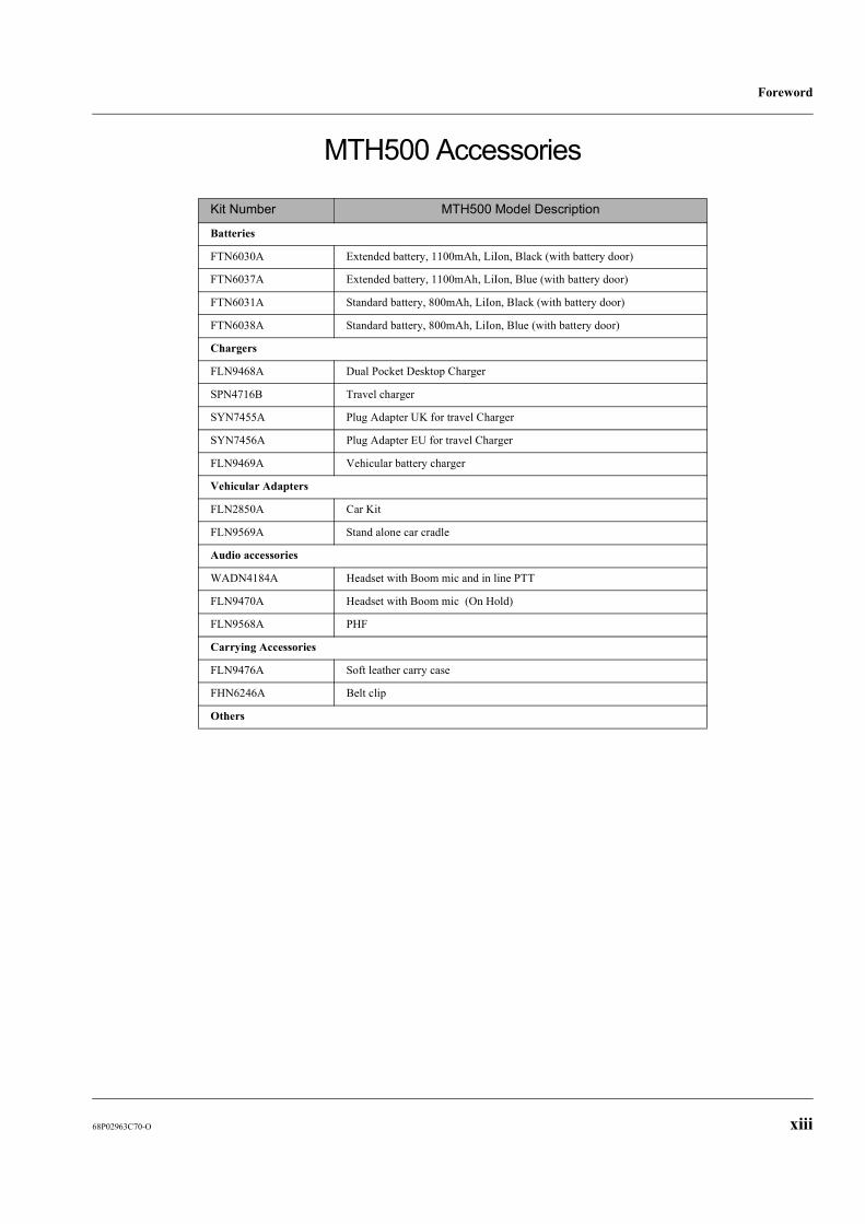
MTH500 Accessories
Kit Number MTH500 Model Description
Batteries
FTN6030A Extended battery, 1100mAh, LiIon, Black (with battery door)
FTN6037A Extended battery, 1100mAh, LiIon, Blue (with battery door)
FTN6031A Standard battery, 800mAh, LiIon, Black (with battery door)
FTN6038A Standard battery, 800mAh, LiIon, Blue (with battery door)
Chargers
FLN9468A Dual Pocket Desktop Charger
SPN4716B Travel charger
SYN7455A Plug Adapter UK for travel Charger
SYN7456A Plug Adapter EU for travel Charger
FLN9469A Vehicular battery charger
Vehicular Adapters
FLN2850A Car Kit
FLN9569A Stand alone car cradle
Audio accessories
WADN4184A Headset with Boom mic and in line PTT
FLN9470A Headset with Boom mic (On Hold)
FLN9568A PHF
Carrying Accessories
FLN9476A Soft leather carry case
FHN6246A Belt clip
Others

Foreword
xiv 68P02963C70-O
THIS PAGE INTENTIONALLY LEFT BLANK

68P02963C70-O 1- 1
Overview
General
To achieve a high spectrum efficiency, the MTH500 uses digital modulationtechnology and sophisticated voice-compression algorithm. The voice of the per-son speaking into the microphone is converted into a digital bit stream consistingof zeros (0) and ones (1). This stream is then modulated into a radio-frequency(RF) signal, which is transmitted over the air to another radio. The process iscalled digital modulation.
Digital Modulation Technology
The MTH500 is a 380-400 MHz portable radio that can operate in dispatch andphone mode. This radio can also operate in TMO (Trunked Mode Operation) andDMO (Direct Mode Operation). It uses two digital technologies: �/4DQPSK andTime Division Multiple Access (TDMA).
�/4DQPSK is a modulation technique that transmits information by altering thephase of the radio frequency (RF) signal. Data is converted into complex symbols,which alter the RF signal and transmit the information. When the signal is re-ceived, the change in phase is converted back into symbols and then into the orig-inal data.
The system can accommodate 4-voice channels in the standard 25 kHz channel asused in the two-way radio.
Time Division Multiple Access (TDMA) is used to allocate portions of the RF sig-nal by dividing time into four slots, one for each unit.
Time allocation enables each unit to transmit its voice information without inter-ference from other transmitting units. Transmission from a unit or base station isaccommodated in time-slot lengths of 15 milliseconds and frame lengths of 60milliseconds. The TDMA technique requires sophisticated algorithms and a dig-ital signal processor (DSP) to perform voice compressions/decompressions andRF modulation/demodulation.
Overview
1 - 2 68P02963C70-O
Voice Compression Technology
Voice is converted into a digital bit stream by sampling the voice at high rate andconverting the samples into numbers, which are represented by bits.
Voice compression reduces the number of bits per second while maintaining thevoice at an acceptable quality level. The MTH500 uses a coding technique calledACELP (Algebraic Code Excited Linear Prediction). The compressed voice-databits modulate the RF signal.
Description
Transceiver Description
All the radio circuitry is contained in the Digital/RF Board and the keypad board.The Digital/RF board is divided into the following sections: digital, frequencygenerating, transmitter, and receiver.
Digital Section Description
The digital section includes the Redcap 2 that consists of the Mcore risk machineand the Digital Signal Processor (DSP).
The Mcore is the controller of the Digital/RF Board. It controls the operation ofthe transmitter, receiver, audio, and synthesizer integrated circuits located in theRF section. It communicates with the keypad and display.
The Digital Signal Processor (DSP) which performs modulation and de-modula-tion functions for the radio. It also performs Forward Error Correction and othercorrection algorithms for overcoming channel errors and ACELP speech coding.It carries out linear 16-bit analog to digital conversions, audio filtering, and levelamplification for the microphone audio input and the received audio output.
The power and audio section is based on the GCAP III and includes power sup-plies, 13-bit CODEC, audio routing, microphone and ear piece amplifiers. A audiopower amplifier is used for the loud speaker.
Transmitter Path DescriptionThe transmitter circuitry includes a linear class AB Power Amplifier (PA) for thelinear modulation of the MTH500. It also includes a novel cartesian feedbackloop to enhance its transmitter linearity and reduced splattering power into adja-cent channels.

Overview
68P02963C70-O 1 - 3
The transmitter path consists of a novel cartesian feedback loop that contains theforward and loop feedback paths. The forward path includes the low noise ODCT(Offset Direct Conversion Transmitter), Balun, Attenuator, and Power Amplifier.The loop feedback path includes the directional coupler, attenuator, and LNODCT(Low Noise Offset Direct Conversion Transmitter) ASIC.
The cartesian Feedback output power passes to the antenna through the Isolator,Antenna Switch, and Harmonic Filter.
Receiver Path Description
The receiver path includes the Antenna Switch, SAW, LNA, ceramic filter, mixer,Crystal Filter, and WPIC (World Phone IC). The first IF consists of the CrystalFilter and WPIC ASIC.
Frequency Generating Section Description
The frequency generating section provides description of the following main com-ponents: Fractional-N Synthesizer, REF. oscillator, Main VCO, WPIC ASIC Syn-thesizers, LNODCT ASIC Synthesizer, External Offset and second LOSynthesizer, DSP PLL, and Host PLL.

Overview
1 - 4 68P02963C70-O
THIS PAGE INTENTIONALLY LEFT BLANK
68P02963C70-O 2 - 1
Theory of Operation
Section Introduction
This section provides a block diagram overview of the main Digital/RF Board.This is supplemented by the detailed block diagram and detailed circuit descrip-tion.
Block Diagram Overview
The main Digital/RF Block contains the following four sections (see Figure 1). Anoverview of these four sections is provided in the following paragraphs:
• Receiver Section
• Transmitter Section
• Digital & Audio Section
• Frequency Generating Section (Synthesizer)

Theory of Operation
2 - 2 68P02963C70-O
Figure 1 General Block Diagram
Receiver Section
The receiver section includes the following main components:
• Antenna Switch
• Limiter
• Front Filter
• Low Noise Amplifier (LNA)
• Second Pre-selector
• Attenuator
• Mixer
• IF Filter
• Balun
• WPIC
DigitalBlock
DCBlock
Transmitter
Receiever
Synthesizer
LCD KeyPad
Audio
Battery
Antenna
AntennaSwitch
Main Board
Theory of Operation
68P02963C70-O 2 - 3
The Receiver Path implements an Automatic Gain Control (AGC). It is requiredto maintain a good receiver linearity over a wide range of incoming signals andprevents clipping of high level signals.
The first Intermediate frequency (IF) circuit consists of the Mixer, IF Filter, andWPIC. The second IF consists of an analog IF and a digital mixer that converts tobase band. They are located in the WPIC. The WPIC performs the following func-tions:
• Carries out amplification and quadrature down conversion of the signal intothe second IF.
• Performs IF AGC.
• Converts the second IF analog signal into digital I & Q formats.
• Synthesizes the second VCO frequency.
• Synthesizes the Sigma-Delta clock.
• Synthesizes the receive and data transmit data clock.
• Transmits the received data to the DSP.
Transmitter Section
The transmitter circuitry includes a linear class AB Power Amplifier (PA) for thelinear modulation of the MTH500. It also includes a novel cartesian feedback loopto enhance its transmitter linearity and reduced splattering power into adjacentchannels.
The transmitter path consists of a novel cartesian feedback loop that contains theforward and feedback paths. The forward path includes the low noise ODCT (Off-set Direct Conversion Transmitter), Balun, Attenuator, and Power Amplifier. Theloop feedback path includes the directional coupler, attenuator, and LNODCT(Low Noise Offset Direct Conversion Transmitter) ASIC.
The cartesian Feedback output power passes to the antenna through the Isolator,Antenna Switch, and Harmonic Filter.
Digital Section
This section includes the REDCAP2, which controls the transmit, receive, andsynthesize operations of the integrated circuits located in the RF section. Withinthe REDCAP2 is the DSP and the serial communication interface.
The digital section contains the following:
• REDCAP2
• Power On/Off circuitry
• Serial peripheral interface (SPI)
• Host memories (flash and SRAM)
• Bottom connector signal MUX
• Keypad block and connector
• LCD (liquid-crystal display) circuit and connector
Theory of Operation
2 - 4 68P02963C70-O
Frequency Generating Section
The frequency generating section contains the following components:
• REF. Oscillator - TCXO
• Main Synthesizer - consists of the WPIC’s PLL and the Main Voltage Con-trolled Oscillator (VCO).
• 2nd Local Oscillator (LO) VCO together with the LMX Dual Synthesizer.
• Offset VCO together with the LMX Dual Synthesizer.

Theory of Operation
68P02963C70-O 2 - 5
Block Diagrams Descriptions
The block diagrams descriptions cover Receiver Path, Transmitter Path, Digital Section, andFrequency Generation Section.
Receiver Path
The received signal (see Figure 2) from the antenna is directed by the Antenna Switch to theFront Filter.
Figure 2 Receive Path Block Diagram
This block-type filter, which defines the receive frequency range, blocks the half IF and imagefrequency entry, and reduces the RF oscillator leakage. The signal is mixed with the local os-cillator to create the first IF at 109.65 MHz. The signal is filtered by the crystal filter and sentto the WPIC ASIC.
The WPIC performs down conversion to the second IF at baseband frequency (0 Hz) and con-verts the second IF analog signals into digital-in-phase (I) and Quadrature (Q) formats. This
(DSP)
LCFront FilterIL=2.5dB
WPIC

Theory of Operation
2 - 6 68P02963C70-O
data is sent for further processing to the Digital Signal Processor (DSP) (part ofRedCap2) over the Synchronous Serial Interface (SSI) data links.
The DSP performs: the demodulation, Forward Error Correction (FEC) and othercorrection algorithms for overcoming channel errors, and the GCAP decoder pro-cedure for digital speech data decompression.
Transmitter Path
When the radio is transmitting (see Figure 3), the microphone audio is sent to theGCAP (CODEC). The CODEC performs analog-to-digital conversion and thedigital signal is routed to the DSP. The DSP performs coding, Error Correction andmodulation. From the DSP, the signal is sent to the WPIC+.
Figure 3 Transmit Path Block Diagram
In the WPIC+ data is converted into analog signal. This signal is also filtered.From the WPIC+, the data is injected to the LNODCT. In the LNODCT the datais mixed with RF signal.
From the differential output of the LNODCT the modulated RF signal is injectedto the Balun-Filter, that transforms the differential input into single output, andthen it is routed to the antenna via the Antenna Switch.
The feedback signal is used for power control.
HarmonicFilter
AntennaSwitch
-0.8dB
-1dB4dB
-8dB
-3.5dB 36 - 39dB
RF PABalun-FilterLNODCTWPIC+
REDCAP2
GCAP
IsolatorAttenuator
Attenuator
Power at Antenna:30dBm ± 2dB

Theory of Operation
68P02963C70-O 2 - 7
Digital Mode of Operation
The digital section (see Figure 4) contains the radio's Redcap Risk-processor withits external memory and DSP, including its memory, within. GCAP III includesswitching regulator and linear regulators, audio preamplifiers, CODEC 13-bit, 8-channel 8-bit A/D Converter, Regulators, Audio Amplifier.
The Redcap controls the receive/transmit frequencies, power levels, display, key-pad, accessories, MMI, and other radio functions. This microprocessor can be op-erated through the RS232 interface by a personal computer to program theFLASH.
The codec distribution is supported by the Global Control Audio Power (GCAPIII) IC. This IC supplies power to the radio using step-down PWM regulator sup-plying 1.88 VDC to the Redcap core, V3 linear regulator 2.775VDC to the exter-nal memories, display and Redcap peripheral modules, supplying V2 to the A/Dconverter, GCAP internal logic, and audio amplifier. The regulator's power-downmode is controlled by the redcap, which senses the ON or OFF condition.
The DSP performs signalling, and voice encoding and decoding. The audio filter-ing and volume control, and analog-to-digital and digital-to-analog conversionson audio signals, are performed in the GCAP's Codec.
.
Figure 4 Digital Section Block Diagram
CS2
OE
EB1
CS0
SPI CE WEOE
FLASHU403
DATA ADR
CE UB LB OE
SRAMU402
DATA ADR
Display
AddressBus
Data Bus
REDCAP2U401
Chip Selects
SPI Bus
RFBus
KeypressDetect
ColumnLines (5)Row
Lines (5)
KeypadBoard
Control Bus
To RadioBottomConnector
RS232
161619
RW
WE
EB0
22

Theory of Operation
2 - 8 68P02963C70-O
Frequency Generating Section
The frequency generating section contains the following components(see Figure 5):
• REF. Oscillator - TCXO
• Main Synthesizer - consists of the WPIC’s PLL and the Main Voltage Con-trolled Oscillator (VCO).
• 2nd Local Oscillator (LO) VCO together with the LMX Dual Synthesizer.
• Offset VCO together with the LMX Dual Synthesizer.
Figure 5 Frequency Generation - Block Diagram
Of fset VCO
Second LO
Dual Synthesizer (U808)
Main VCO
Main Synthesizer
493.65-513.65 MHz to RX Mixer
113.65 MHz to Offset Mixer
493.65-513.65 MHz to TX MixerReferenceOscillator - TCXO
Divider
OSC_IN
DOI F
IF Section
RF Section
DORF219.3MHz
FINIF
FINRF
50kHz
100kH zOSC_IN
WPI CXTALBASE
PRSCI N
CPGITR
Data
LOIN
LPF
LPF
LPF
Osc.
Osc.
Osc.
Buf fer
Theory of Operation
68P02963C70-O 2 - 9
All frequencies originate from the REF. oscillator -TCXO. This is a digital tem-perature compensated crystal oscillator producing an accurate and stable 16.8MHz reference frequency. The 16.8 MHz reference frequency is divided in theWPIC and in the Dual Synthesizer to produce required reference frequency for theother synthesizers.
Main Synthesizer
The Main Synthesizer consists of the WPIC internal PLL modules, and MainVCO on board. It produces the LO signal to down-convert the receive signal to thefirst IF 109.65 MHz frequency and to up-convert the 113.65 MHz transmitter IFfrequency to produce the RF carrier frequency.
RX Second Local Oscillator (LO)
The second LO synthesizer supplies the second IF local oscillator frequency to thereceiver. It produces 219.3 MHz that is divided by two in the WPIC in order todown-convert the received signal to the baseband.
Offset VCO
The Offset VCO consists of the LMX Dual Synthesizer and the VCO on board. Itproduces the output of the offset VCO 113.65 MHz.

Theory of Operation
2 - 10 68P02963C70-O
Detailed Circuit Description
Receiver Path, Detailed Circuit Description
See Figure 6.
Figure 6 Receiver Path Circuit Diagram
Antenna Switch
The signal coming from the antenna is routed to the receiver section via the har-monic filter, which is comprised of L890 and C1012. The signal continues to flowthrough image filter (equivalent quarter wave) transformer C1015 and L817 to theRx section toward limiter diode D500. The antenna switch attenuates the image
(DSP)
BasebandFilters
BasebandAmplifiers
LCFront FilterIL=2.5dB
GCAP
Theory of Operation
68P02963C70-O 2 - 11
frequency by approximately 38dB. The attenuation of wanted signal is typically0.7dB.
Limiter
The limiter (D500) function is to prevent entering of signal with power higher then30dBm, which may damage the receiver front-end.
Front Filter
The signal arrived from the limiter is flowing via the front filter (FL500) and rout-ed to the Low Noise Amplifier (LNA) (U500) via C576.
The front filter is also called -1st pre-selector and is used to attenuate the incomingparasitic RF frequencies, especially the image frequency (25dB). The InsertionLoss (IL) is typically 2dB.
LNA
The LNA module is the RF signal amplifier. The LNA gain (U500) including out-put matching circuit, C1048, L518, C521, R965, L500, C532, R580 and C507, istypically 23dB. Because the LNA is the first amplifier in the line, it is importantthat it will maintain large gain and small Noise Figure - 1.8dB.
The LNA has an “enable” pin (pin 3) which is called VPD. When this pin receivesa supply of 1.8 V from DC switch (Q504) - the amplifier is enabled. From theLNA the signal passes to second pre-selector, LC filter (FL501). The IIP3 of theLNA is between -5dBm to -2.5dBm.
Second Pre-selector
The 2nd Pre-selector (FL501) attenuates the non-linear products of the LNA andalso the image product by 25dB. Its IL is typically 2.5 dB. From the output of theLC filter the received signal is routed via a Pi-attenuator to the Mixer RF input.
Attenuator
The purpose of the resistor Pi-attenuator (R519, R517, R945), is to protect themixer (U504) input from saturation. The pad attenuates RF power by 2.5dB
Mixer
The Mixer (U504) function is to down convert the incoming RF signal into IF sig-nal (109.65 MHz). The Conversion Loss (CL) is typically 6.2dB and its IIP3 istypically 20dBm.
The RF signal enters the Mixer at pin 1, and the IF is produced at pin 6. The LO(from the main VCO) signal passes via the matching circuit (C522, L505, R943

Theory of Operation
2 - 12 68P02963C70-O
and C984), enters the Mixer at pin 3. The LO power at the LO mixer input is -2dBm. The 2.7V DC is supplied by switch Q500 to pin.4.
The mixer conversion Loss is 7dB.
An impedance matching net is placed between the mixer and the IF filter (FL502).It consists of L512, C525, C531, C524, L504 and C539.
IF Filter
The IF signal is routed via the IF filter (FL502), which has IL of 2.5dB and atten-uates parasitic products of the Mixer, and via an impedance matching network thatconsist of C546, C536 and L501 to the BALUN.
BALUN
The Balun transforms the single ended input RF signal to a differential double-ended output. It consists of L519, C526, C527, L520, C530 and C534.
The differential signal is routed to the WPIC (Word Phone IC) at pin A4 and B4.
WPIC (receiver section)
The differential IF signal is amplified and transferred into the WPIC and mixedwith 2nd LO signal. The 2nd LO signal is routed to the WPIC at pin D1 and divid-ed by 2 in to the quadrature generator block of the WPIC. The baseband signalfrom the mixer passes via a Baseband filters and amplifiers arrays that gives lowernoise and better I & Q balance, to the WPIC A/D block and than to the DSP.
An internal AGC that is controlled by a control unit, establishes an appropriate at-tenuation for unwanted signals as well as an appropriate gain for wanted signals.The voltage at external capacitor C557 indicates the AGC attenuation level for thedifferent input signal levels. The voltage at the capacitor varies from 1.4V to 2.7Vas a function of the power of the received signal.

Theory of Operation
68P02963C70-O 2 - 13
Transmitter Path, Detailed Circuit Description
See Figure 7.
Figure 7 Transmit Path Circuit Diagram
Forward Path
WPIC
The WPIC (World Phone IC) U503 receives serial data that is transmitted by theREDCAP2 at a 48 kbps rate to the SSI port (pin K10, STD). Data is transmittedas a 16-bit ‘I’ word followed by a 16-bit ‘Q’ word. The WPIC provides a serialclock of 4.8MHz to the REDCAP2 (pin K11, TXCLK) and sends a frame sync sig-nal (pin L11, RXFS/SFS) at the beginning of every ‘I’ word transmission, to in-struct the REDCAP2 to send data. In the WPIC, the received serial I & Q wordsfrom the REDCAP2 are converted into parallel I & Q words, and transferred to aninterpolating filter. The interpolating filter increases the sampling rate to reducein-band quantization noise, as well as to reduce image at multiples of the input da-ta. The interpolated samples are rounded to 8 bits, and run through the 8-bit D/Aconverters. The D/A converters take the digital I & Q words and convert them intoanalog signals, which are filtered and amplified. The output is comprised of twoseparate low-level differential signals, I & Q (pins A8, OUTQ; C8, OUTQB; D8,OUTI; A9, OUTIB). A differential output is used to minimize the noise pick-up,due to its inherent common mode rejection. The output signals are routed to theLNODCT IC where the transmitting loop is closed. The WPIC sends a 2.4MHz
LNODCT
Balun-Filter
Att.
+30
Att.
0
-3dB
37 ± 2
-5dB
-10dB
I/Q Split
Dr
ImageFilter Att.
-3
Main VCO
Mixer
WPIC(ADDAGpart)
REDCAP2
Power Amp.(FET)
Coupler
Isolator
Ant. Switch+Harm.Filter
OffsetVCO
DualSynthesizer
-0.1dB

Theory of Operation
2 - 14 68P02963C70-O
low-level differential reference clock signal (pins B11, TCLCK; C10, TCLCKB)to the LNODCT. It also sends a differential signal (pins A11, TSLOT; A10,TSLOTB) that marks the beginning and the end of each transmission time slot ofthe REDCAP2 (whenever a TXE signal (pin H8 TXE) is received from theREDCAP2). After receiving the TSLOT signal, the LNOCDT toggles the ASWline (pin J5, ASW) which signals the WPIC to set VCNTO signal LOW (pin J6,VCNTO) which enables the Antenna Switch during transmit time. WPIC starts toreceive data from REDCAP2 after TXE signal (pin H8, TXE).
LO LINE-UP
LO LINE-UP includes MIXER U800, Attenuator (R800, R819, R808), Image Fil-ter FL800, LO Driver Q808, and I - Q Splitter Q801. Offset VCO is based on DualSynthesizer IC U808 that receives data from REDCAP2 that defines Offset VCOparameters. The Offset VCO signal 113.65MHz is mixed with the Main VCO sig-nal (493.65 - 513.65MHz) in the Mixer U800. The output of the Mixer is the RFcarrier frequency. The signal passes through the ��attenuator and image filterFL800. The image filter attenuates the VCO and image frequencies and any out-of-band spurs that may be present. The signal is amplified by LO FET DriverQ808 and routed to I-Q splitter U801 that converts the single input signal into twoquadrature (90 degrees phase shift) ‘I’ and ‘Q’ signals and then routs them to theLNODCT LO input (pins 46, LOQ; 45, LOQB; 57, LOI; 56, LOIB). RF signal issampled at the I-Q splitter input and applied to the LNODCT LO feedback (pin24, MVCO).
LNODCT
The LNODCT (Low Noise Offset Direct Conversion Transmitter) U803 is theheart of the transmitter.
The differential base-band signals from the WPIC are inputted into the LNODCTon pins 58 – 61 (BINQB, BINQ, BINIB and BINI). They pass through a variableattenuator and then they are summed with the down converted I & Q feedback.The base-band signal is then amplified and sent to the up-mixer.
The up-mixer consists of two mixers, one for the I channel and the other for the Qchannel. The split I & Q LO signal is mixed with the base-band I & Q signals toproduce an I and Q modulated signals at RF frequency. The signal is then outputdifferentially on pins 51 and 52 (RFOUTB, RFOUT).
BALUN - FILTER
The differential RF signal is converted to a single-ended (unbalanced) signal bypassing the BALUN-Filter FL801 (balanced-unbalanced filter). The BALUN-Fil-ter has a 200 Ohm input and 50 Ohm single-ended output, the BALUN-Filter out-put voltage amplitude is two times higher than the differential voltagesamplitudes. Thus the LNODCT output signal is increased by 6dB in compare toeach of the differential signals.
Theory of Operation
68P02963C70-O 2 - 15
Another function of the BALUN-Filter is to attenuate the image frequencies andother unwanted out-of-band spurs present in the output signal. The insertion lossof the BALUN-Filter is 3dB. The output signal from the BALUN-Filter is appliedto the RF PA through -1.8dB attenuator (R836, R833, R834).
RF Power AmplifierThe signal is then routed through DC coupling capacitor C823 to the RF PowerAmplifier (PA). The PA IC consist of two amplifying stages. The PA output ismatched with 50 Ohm coupler by the ��LC-circuit (C1028, C1029, L921). LCnotch filter (L923, C1030) rejects the second harmonic of the RF signal. The PAgain is set by PA_BIAS voltage from the REDCAP2, L1T 3 (pin C6, TOUT3).The bias voltage is applied to the dual-transistor switch Q807, Q911 and then toPA (pins 8,VREG; 16, VBIAS respectively).
Coupler and Feedback PathA coupler U806 exists at the RF PA output, it is used to pass the signal to IsolatorFL801 and sample the signal thus providing the necessary feedback for the line-arization and feedback correction. The sampled signal is routed via attenuatorR815, R818, R825 to the LNODCT (pin 37, RFIN). The feedback signal is thenmixed down to base-band in a quadrature down mixer, amplified and summedwith the base-band input signal. The loop is closed.
Isolator
The signal in the forward path is fed to pin 2 of the isolator (FL801). The isolatoris placed at the PA output to decrease the influence of the antenna impedance var-iation on the PA performance. The reflected power returned from the antenna, isabsorbed in a 50 Ohms resistor inside the isolator. The isolator also protects theCartesian loop from sudden VSWR variations that could lead to loop instability.
Antenna Switch
The RF signal from the Isolator is applied to the PIN DIODES U802. The PIN di-odes are turned on during the transmission time slot, and the DC current flowsthrough the Isolator to the ground. The RF signal is routed through 2 �-LC-cir-cuits (C848/L818/C838 and C1010/L817/C852) and the Harmonic Filter to theAntenna. L817/C1015 circuit provides the image rejection of the output RF signal.In the Receiving mode the PIN diodes are turned off, the input RF signal is direct-ed to the receiver path via p/4 LC equivalent circuit (C1010/L817/C852). The con-dition of the PIN diodes is controlled by the voltage switch Q806 by applying theANT_EN signal to the switch. The resistor R832 determines the DC currentthrough PIN diodes; diode D801 provides the additional capacitance during theTransmission mode, capacitors C835 and C832 compensate the parasitic induct-ance of the D801. The VCNTO signal applied to the voltage switch Q806 is setLOW during the Receiving and Transmission modes.
The RF output signal is disabled during the CLCH (Training) mode by setting theVCNTO signal HIGH thus providing the low output power during the trainingslot.
Theory of Operation
2 - 16 68P02963C70-O
Harmonic Filter
From the antenna switch the signal is routed to a one section of LC filter, consist-ing of the coil L890 and capacitors C1010, C1011 and C1012. The filter is re-quired to attenuate the harmonics of the amplifying stages at the transmissionpath, and the Local Oscillator leakage at the receiver path.

Theory of Operation
68P02963C70-O 2 - 17
Digital Section, Detailed Circuit Description
See Figure 8.
Figure 8 Digital Section - Detailed Circuit Diagram
Host Memories
The RedCap2 Address bus is a 22-bit wide (0:21) and RedCap2 Data Bus is a 16-bit wide (0:15).
RedCap2 uses two types of memories:
Flash Memory
The Flash Memory is dedicated to the application software. This memory has a16-bit wide data bus. The Flash memory location has a 32M Bit of memory; Whenaddressing the Flash memory location, the processor reads into its 16-bit wide databus.
RF Section
GCAP3
CE Accessory Conn.
Keypad
Vibracall
Power Supplies
Radio Off
ES
SI
UA
RT
OP
TS
EL
ESSISPIBReset
OPT B+
USB/8-RS232
USB_PWR
BAT_FDBK
Ext Audio
ON3
Control
BBP
SPIA
REDCAP2
4 MB flashmemory1MB SRAM
Graphic Display
SPIB

Theory of Operation
2 - 18 68P02963C70-O
The Flash also stores the Radio CodePlug (Customer related information) such astelephone numbers, addresses, etc.
SRAM Memory
This 512 x 16 Static Ram is used for Data storage.
Serial Peripheral Interface (SPI)
The RedCap2 uses the SPI protocol (Serial Peripheral Interface) to communicatewith RF IC's (WPIC, ODCT, Synthesizer/LMX), GCAP3 IC and the display driv-er.
The RF IC's are connected to SPIA module, while GCAP3 and the display areconnected via SPIB module.
The protocol is built upon 4 lines [MOSI(Tx), MISO(Rx), CS, CLK)].
The Display Module, based on the display driver (i.e. Samsung KS0741) uses aserial interface.
Figure 9 is a block diagram of the RedCap2 and its interfaces.

Theory of Operation
68P02963C70-O 2 - 19
Figure 9 REDCAP2 Block Diagram
Encr yptionAccelerator
DSP Peripheral DMA
PR OM 2Kx24
PRAM 40Kx24
YROM 0Kx16
YRAM 15Kx16
DSPCore
ViterbiAcceler ator
MCU/DSPInterface
MDI
XROM 0Kx16
XRAM 12Kx16
Shared X/VIA CRAM 2Kx16
Shared X/MCURAM 2Kx16
Clocks/PLL
MCU Debug
Layer 1Timer
JTAG/OnCE
UARTB
MUX
UARTA
AudioCODECSer ial PortSAP
BRM
ExternalIntefaceModule
QSPIB
QSPIA
SIM
Reset
KeypadInterface
GPIO
MCUCore
ROM 4Kx32
RAM 512x32
PIGPeripher al I/F
Gask et
GPReg
MCU Timers/PWM/PIT/Watchdog
BasebandCODECSer ial P ortBBP
Counter
DSP Timer
MC
U I
nt. C
t l
DSP_IRQSTDB
SRDBSFSB(2)
SCKB(2)
STD ASRD A
SFSA(2)
SCKA(2)
ADRS(22)
DATA(16 )R/WOE
EB0,EB1CS(6)MOD
INT(6)INT6/DSRA/STD A/TRST
INT7/DTRA/SCLK/SRD A/TMS
MOSIBMISOBQSCKB
SPICSB(5)
MOSIAMISO A
QSCKASPICSA(5)
RST_OUTRST_IN
COLUMN(5)ROW(5)
COLUMN5/GPIOROW5/IC2B/GPIO
COLUMN6/OC1COLUMN7/PWM
ROW6/DCDA/SC2A/DSP_DEROW7/RIA/ISCKA//TCK
XYA(16)
XYRW,XYSEL,XYSTB
XYD(16)/TXA/RXA/GI
CKIH,CKILCKOH,CKO
DEBUG(6)
TOUT(16)
DSP_DEJTAG(5)MCU_DETESTRTSBCTSBTXBRXB
MUX_CTLRTSA/IC2A/RESET_INCTSA/MCU_DE
TXA/TDO
RXA/IC1/TDI

Theory of Operation
2 - 20 68P02963C70-O
DC Power Distribution
(See Figure 10).
V1 Linear Regulator
V1 is a programmable linear regulator. It is programmed using the Redcap SPI busfrom 0.975V to 3.0V in 8 steps. This regulator is active during Power Reset (POR)and its initial value is 0.95V. For this radio, V1 (programmed to 1.875V) is thesupply for the vibrator motor. This regulator is active whenever the radio is turnedON.
V2 Linear Regulator
V2 is a selectable linear regulator. It is selectable using the GCAP UV_SEL pinbetween either 2.5V and 2.775V. This regulator is active during POR and its initialoutput value is set by GCAP3 UV_SEL pin. Connecting UV_SEL pin to B+ setsV2 output value to 2.775V, connecting UV_SEL pin to Ground sets V2 output val-ue to 2.5V. For this radio, V2 is selected to 2.775V. This regulator is supplied byB+ and it is active whenever the radio is turned ON. V2 is the supply for internaland external audio circuits, CLK_IN input driver and TS interface.
V3 Linear Regulator
V3 is a selectable linear regulator. It is selectable using the Redcap SPI bus from1.875V to 2.775V in 4 steps. This regulator is active during POR and its initial out-put value is 2.775V. For this radio, V3 is selected to 2.775V. The regulator is sup-plied by B+ and it is active whenever the radio is turned ON. V3 is V3_2.775V,which is the supply for the SRAM, FLASH, Redcap, CE bus and Display.
V4 Linear Regulator
V4 is a selectable linear regulator with external pass transistor. It is selectable us-ing the Redcap SPI bus from 1.875V to 2.775V in 4 steps. It is set to 2.775V. V4is always powered from B+ and it is active whenever the radio is turned ON. Thisregulator is active during POR. V4 is V4_2.775V_RF, which is the supply for theWPIC, ODCT and LMX.
Switcher #1 (Synchronous Buck Mode Converter)
Switcher #1 is a selectable step down switching regulator. It is selectable using theRedcap SPI bus from 1.2V to 2.45V in 6 steps, Pass Through and Power downmodes. The switcher is active during POR in 1.86V mode. It is set to 1.86V.Switching regulator is PWM#1_1.86V, which is the supply for the internal core,emulation port and clock output drivers of the Redcap. The switcher is suppliedfrom B+ and it is active whenever the radio is turned ON.
Theory of Operation
68P02963C70-O 2 - 21
Switcher #2 (Boost Mode Converter)
Switcher #2 is a selectable step up switching regulator. It is selectable using theRedcap SPI bus to 5.6/5.0/3.35 Volt and Power down mode. The switcher is sup-plied from B+ and it is active whenever the radio is turned ON. The switcher isinherently in 5.6V mode at POR. The radio uses the switcher at 5.6 V to supply5V_RF and VSIM linear regulators.
DSC Linear Regulator
DSC is a fixed output linear regulator. This regulator is active during POR in the5V mode. DSC is supplied from PWM#2_5.6V, which is used to supply the WPICand ODCT charge pump circuits.
TS_REF Linear Regulator
TS_REF is a fixed output linear regulator. It is supplied internally from the V2 lin-ear regulator. It is set to 2.3V. The radio uses TS_REF for the AD voltage dividers.It is not active at POR.
VREF1 Linear Regulator
VREF1 is a programmable linear regulator. It is programmed using the RedcapSPI bus from 1.875V to 2.775V in 4 steps. This regulator is active during POR andits initial value is 2.775V. For this radio, VREF1 is programmed to 2.775V and isbattery supplied. VREF1 is VREF1_2.775V, which is the supply for TCXO.
VREF2 Linear Regulator
VREF1 is a programmable linear regulator. It is programmed using the Redcap SPI bus from 1.875V to 2.775V in 4 steps. This regulator is active during POR and its initial value is 2.775V. For this radio, VREF2 is programmed to 2.775V and is battery supplied. VREF2 is VREF2_2.775V, which is the supply for the keypad and display backlight circuits. This regulator is On whenever the radio is turned ON.
Current Limit
The SWB+ current limit regulator provides power from the phone battery to clip-on accessories. It is enabled only when the phone is powered up and an accessorywhich requires power from the phone is connected.
Several sections of the radio are connected directly to the battery, which suppliesRaw_B+ and Fused_B+. The radio operates with a low-level battery voltage of3.15Vdc, nominal-level voltage of 3.6Vdc, and high-level voltage of 4.2Vdc. Thebattery is connected to P1 - 4 (+) and P1 - 1 (-). These pins supply the Raw_B+to the RF TX power amplifier. The SWB+ output of the U104 regulator suppliesthe accessories through the bottom connector. Raw_B+ is routed via F600 (Fuse)

Theory of Operation
2 - 22 68P02963C70-O
becoming Fused_B+, which goes via the main FET and provides power to theGCAP III IC.
Figure 10 MTH500 DC Distribution
Bat
tery
Fil
ter
3.6VDC
RF PATetra
Filter
Filter
Filter
PWM2(Boost)5.6V @ 100mA
V32.775V @ 150mA
PWM1(Buck)1.86V @ 100mA
EXT_VSIM13.0V @ 50mA
CurrentLimit800mA
VREF12.775V @ 5 mA
V22.775V @ 200mA
V11.875V @ 150mA
VREF22.775V @ 100mA
V42.775V @ 250mA
VDSC5V @ 60mA
VTS2.3V @ 5mA
VVIB1.3V @ 200mA
VUSB3.3V @ 40mA
ON
ON
ON
OFF
OFF
OFF
ON
0.9V OFF
0.95V OFF
1.875V ON
ON
ONFILT_B+ V4_2.775V_RF
V4_2.775V_RF
FILT_B+
VREF2_2.775V_RF
WPICSFOUT:2.5V, 40mA
MainVCO&BufferOffsetVCO
: 10mA:
7mA
VCO&Buffer2ndLOVCO
: 10mA:
7mA
5V_RF
TETRATX
TETRATX
WPICCP5
Driver&mixer45
TETRARXWPIC: 20LNODCT: 130Mixer:2.5AntSW: 8LO_DRV: 40
TETRA_TX:202TCXO: 2
WPIC: 30Mixer:2.7LNA:7.5
TETRA_RX:62Dedicated: 2.5
VBLIN: 3ODCT CP: 1PA Bias: <1
REDCAPAVDD-AddressBusDVDD-Data BusCVDD-Bus ControlBVDD-SIMEVDD-AudioESSI
HVDD-SPIA/B,BBESSL,L1TLVDD-DSPAddress Bus VisibilityMVDD-DSPData Bus Visibility
FVDD-ClockOutputDriverKVDD-EMULPort
OVCCH-I/Opre driversvoltage
OVCC-Internalcore
GVDD-GPIO,JTAG, DebugSTO, DATA, Bottom
FLASHVCC
SRAM
AUDIO PA
Vibrator
Accessory VCC
Audio Circuits
USB Drivers
BL_SNKGCAP III
V3
SWB+ EN
UV_SEL
USBDETECT
ThermBatt,RF_PA Term,HW_ID
Keypad/DisplayBacklight
Display
R_G_LED
MA
IN-B
OA
RD
KE
YPA
D
LEDR/LEDGGCAP III
LNODCT:Upmixer40mA
TCXO: 2mA
NotUsed

Theory of Operation
68P02963C70-O 2 - 23
RS232, SB9600
The REDCAP processor (RCE) uses the three serial protocols: UART andSB9600 to communicate with external devices via the bottom connector of theunit. There is no external hardware for switching from one protocol to another be-cause the REDCAP2 handles the switching and line multiplexing functions inter-nally.
Battery ID
The battery is equipped with a Dallas 2502 EPROM. A one-wire serial bus allowsthe radio or the battery charger to communicate with the battery and identifywhether or not the battery is compatible. If the battery is determined to be incom-patible, the unit automatically shuts off, and the charger does not enter chargingmode.
Besides compatibility data, the EPROM also stores the following information:battery type, capacity, fuel-gauging parameters, and voltage threshold.
Radio Audio System
See Figure 11.
The audio system consists of the GCAP 3 IC (U600) and the DSP (U401), bothare located on the main board.
The GCAP 3 perform the analog task and part of the digital task of the audio sys-tem.
Tx Path
Audio speech is fed either to the internal microphone, or to a Phone Hands Free(PHF) microphone. The signals reach the GCAP 3 IC. In the GCAP 3 IC, a fix gainamplifier (A3 or A5) provides the signal amplification, the multiplexer (MUX) se-lects the active input, and the programmable Gain Amplifier (TxPGA) adjust thepath gain according to the radio mode of operation. Finally, the A/D converts theanalog signal into digital format and transfers it to the DSP. The DSP performs thefunctions of audio filtering, ACELP speech compression, digital modulation, andtransfers the data to the RF section. When the radio is operating in the telephoneinterconnect mode, the DSP performs the required tasks such as echo and noisereduction.
Rx Path
The digital output signal from the receiver is fed to the DSP which performs thefunctions of digital de-modulation, ACELP speech de-compression, and audio fil-tering. It transfers the data to the GCAP3 IC. In this IC, the D/A converts the dig-ital audio format to an analog signal, the Programmable Gain Amplifier (RxPGA)

Theory of Operation
2 - 24 68P02963C70-O
GCAPIII
adjusts the path gain according to the setting of the volume control, and the mul-tiplexer routes the audio to the active receive path. When the internal speaker isactive, the audio is fed to A2, double-ended audio power amplifier. Otherwise, theaudio is fed to A1, output amplifier, that drives the Internal Earpiece or the PHFearpiece.
Figure 11 Audio Path Block Diagram

Theory of Operation
68P02963C70-O 2 - 25
Frequency Generating Section Detailed Circuit Description
See Figure 12.
This section describes the generating circuits that supply all the required frequen-cies for the required transmitter and receiver functions. These circuits are de-scribed as follows:
• REF. Oscillator - TCXO.
• Main VCO and Main Synthesizer.
• Second IF VCO and Dual Synthesizer RF section.
• Offset VCO and Dual Synthesizer IF section.
Figure 12 Frequency Generating Section - Block Diagram
Of fset VCO
Second LO
Dual Synthesizer (U808)
Main VCO
Main Synthesizer
493.65-513.65 MHz to RX Mixe
113.65 MHz to Offset Mixer
493.65-513.65 MHz to TX MixerReferenceOscillator - TCXO
Divider
OSC_IN
DOI F
IF Section
RF Section
DORF219.3MHz
FINIF
FINRF
50kHz
100kH zOSC_IN
WPICXTALBASE
PRSCI N
CPGITR
Data
LOIN
LPF
LPF
LPF
Osc.
Osc.
Osc.
Buf fer

Theory of Operation
2 - 26 68P02963C70-O
REF. Oscillator - TCXO
The TCXO is the reference frequency source for all the radio synthesizers. Theoutput of the oscillator is a 16.8 MHz stable temperature compensated referenceclock. This signal is present at pin 3 of the TCXO. This oscillator’s centre frequen-cy is programmed (256 steps of approximately 0.1 ppm). It drives the TCXO buff-er to split the 16.8 MHz signal to the WPIC, LMX Dual Synthesizer and GCAPIII.
The 16.8 MHz signal from pin 3 of the TCXO is routed into the following:
1. The WPIC via C580 to pin K6 XTALBASE. The signal is divided by 4 to produce the 4.2 MHz reference signal, which is used for the Main PLL syn-thesizer.
2. The LMX Dual Synthesizer via C946 to pin OSC_IN. The signal is divided to produce the 100 KHz reference signal for the second LO and to 50 KHz reference signal for the Offset VCO.
Main VCO and Main Synthesizer
The synthesizer components are WPIC, Loop Filter, VCO and buffer. It producesthe LO signal.
The synthesizer functions are as follows:
• To serve as the local oscillator for the mixer of the receiver. It is used to down-mix the RF frequency (109.65 MHz).
• To serve as the LO for mixing the transmitter IF frequency (generated by the Offset VCO) into the transmit RF band. The transmitter Offset VCO fre-quency is 113.65 MHz. This conversion is performed in the Tx Mixer.
• To serve as the WPIC feedback signal for locking the main synthesizer.
The WPIC is programmed by the DSP through the SPI bus.
WPIC
The WPIC contain internal synthesizer loops:
1. The main PLL is a three accumulators, fractional N system with a 24-bit resolution. The 16.8 MHz signal from pin 3 of the TCXO is routed via C580 to pin K6 of XTALBASE input of the WPIC. In the synthesizer, the signal is divided by 4 to produce the 4.2 MHz reference signal used for the main PLL synthesizer.
2. The second LO generator, which has a single ended signal at twice the de-sired IF frequency. The signal is routed as a differential signal (I, Q) to a quadrature phase splitter at the WPIC. The quadrature generator is a single master-slave flip-flop configured in a divide by two toggle mode.

Theory of Operation
68P02963C70-O 2 - 27
LMX - Dual Synthesizer
The LMX233XL is an integrated dual frequency synthesizer that includes prescal-ers. It is used with the second LO at the RF section and with the Offset VCO at theIF section.
The LMX uses the 16.8 MHz from the TCXO for both synthesizers and dividesthe TCXO frequency as follows:
• The reference frequency for the second LO is 100 KHz.
• The reference frequency for the Offset VCO is 50 KHz
Second LO VCO
The Second LO VCO is a discrete VCO that is controlled by the LMX Dual Syn-thesizer RF section. The VCO produces a frequency of 219.3 MHz.
The internal phase detector is of the charged pump type.
The output signal of the of the VCO is routed via the phase detector at U808,pin 5 (FINRF).
The output of the phase detector is present at U808, pin3 (DORF) and than via theloop filter R915, C903, C948.
Offset VCO
The Offset VCO is a discrete VCO that is controlled by the LMX Dual Synthesizer(U808) IF section. The Offset VCO produces frequency of 113.65 MHz.
The internal phase detector is of a charged pump type. The output signal of theVCO is routed via the phase detector at U808, pin 18 (FINIF).
The output of the phase detector is present at U808, pin 20 (DOIF) and than viathe loop filter R829, C895, C860.

Theory of Operation
2 - 28 68P02963C70-O
Display and Keypad Description
Display
The LCD (Liquid Crystal Display) Module is a Graphic Display based upon theKS0741TB-01 display driver.
It consist of LCD Holographic Glass, LED backlight and a 22 pin flex cable con-nected to the Keypad board.
The Communication to the RedCap2 IC is performed using a SPI protocol (SerialPeripheral Interface). The Operation of the LCD is determined upon the RS lineconfiguration (Data/Command).
The Display is 128X100 (Columns X Rows respectively).
Keypad
The RCE is responsible for decoding key presses and displaying them properly onthe LCD. The keys are arranged into a matrix of five rows and five columns, whichincludes the Volume and PTT keys.
The PWR key is not decoded by the RCE; it directly drives the GCAP III, whichsends a signal to RCE through INT1. The five row lines are pulled high via fiveinternal 22 Kohm resistors. The five row lines and five column lines are fed toREDCAP2 I/O pins. Pressing any key also generates the keypad internal interrupt.The REDCAP2 debounces the keys by reading them 25 milliseconds later.
The keypad-decoding scheme works as follows:
1. REDCAP2 sets rows to inputs; all columns are set as outputs and driven logic low.
2. Rows are pulled logic high. When a key is pressed, one row goes low, which indicates a key press and sends an internal interrupt.
3. REDCAP2 reads rows. A low on that row indicates a key press. All others are high.
4. REDCAP2 sets all columns to output logic high.
5. One column at a time is set to output logic low. REDCAP2 reads the rows to see which one is now at a logic low level. (A low seen on a row indicates the correct column and row.)
All keypad circuitry is located on the keypad board. Refer to the keypad boardschematics.

Theory of Operation
68P02963C70-O 2 - 29
Backlight and LEDs
Backlight
The keypad backlight consists of 10 green LEDs. There are two more LEDs in theLCD module that are connected in parallel to the keypad LEDs.
Top LEDs
There are one Green and one Red LEDs, both located on the LCD board. TheseLEDs are used as indicators to the radio operation.
Radio Programming
The radio is entered into programming mode by setting the MOD pin high level,and applying a preamble sequence to the radio via the RS232 lines.
The MOD pin assertion is encountered at least 4 CKIH cycles before the negationof the Reset pin.
Accessory Connector
The CE bus is intended to support connection to accessories, personal computers,and test systems. The bus connector has a total of 17 pins, 9 of which have multi-ple functions. The bus has six basic modes of operation: Normal (also No Acces-sory Connected), USB Mode, Analog Audio Mode, Phone Powered USB Mode,RS-232 Mode, and RS-232/SSI Mode (there is also two additional non-standardmodes, DSC and FLASH which are used only for development, factory program-ming, and debugging). Eight of the 17 pins have different functions depending onwhich mode is selected. The other 9 pins always have the same function regardlessof mode.
The mode is selected by applying appropriate logic levels to the Option Selectpins, named OPTION1 and OPTION2. Some of the modes listed above are select-ed by the additional application of a level on the USB POWER and AUDIO-INpins as well.

Theory of Operation
2 - 30 68P02963C70-O
Mode Select (OPTION1 and OPTION2)
Logic levels applied to the OPTION1, OPTION2, USB POWER, and AUDIO IN lines areused to select the CE Bus mode. The modes will be set as follows:
MODE OPTION_1 OPTION_2 USB_PWR AUDIO_IN
NORMAL (no accessory) 1 1 0 X
USB Accessory/Computer 1 1 >4.0V X
Dumb Accessory 1 0 X 1
Phone Powered USB Accessory 1 0 X 0
RS-232 (8 wire)/IDB Smart Cable 0 1 X 1
RS-232 (4 wire)/SSI 0 1 X 0
PTT 0 0 X X
SB9600 X X
Pin No. Signal Name (Short Form)
Power/Default States
USB Dumb RS232/SSI
RS232 (8
wire)
1 Power Ground (GND) GND GND GND GND GND
2 Battery Feedback (BATT_FDBK) BATT_FDBK
BATT_FDBK
BATT_FDBK
BATT_FDBK
BATT_FDBK
3 External Power (EXTB+) EXTB+ EXTB+ EXTB+ EXTB+ EXTB+
4 USB+/TXD (D+) D+ TXD TXD TXD
5 USB-/RXD (D-) D- RXD RXD RXD
6 USB Power/Ignition/RTS (USB_PWR)
USB_PWR
IGN RTS RTS
7 Switched Battery (SWB+) SWB+ SWB+ SWB+ SWB+ SWB+
8 Hook Switch/CTS (HKSW) HKSW HKSW CTS CTS
9 MUTE/FS/DCD (MUTE) MUTE FS DCD
10 DUMB_SEL2/SCK/RI (DSEL2) DSCEN DSCEN DSEL2 SCK RI
11 DUMB_SEL1/SRDA/DTR (DSEL1)
DSEL1 SRDA DTR

Theory of Operation
68P02963C70-O 2 - 31
12 DUMB_SEL0/STDA/DSR (DSEL0)
DSEL0 STDA DSR
13 Option 1 (OPT1) UPLink UPLink OPT1 OPT1 OPT1
14 Option 2 (OPT2) DNLink DNLink OPT2 OPT2 OPT2
15 Audio Out On/Off (AUDIO_OUT) AUDIO_OUT
AUDIO_OUT
AUDIO_OUT
AUDIO_OUT
AUDIO_OUT
16 Audio In (AUDIO_IN) AUDIO_IN
AUDIO_IN
AUDIO_IN
AUDIO_IN
AUDIO_IN
17 Audio Ground (AUDIO_GND) AUDIO_GND
AUDIO_GND
AUDIO_GND
AUDIO_GND
AUDIO_GND
Pin No. Signal Name (Short Form)
Power/Default States
USB Dumb RS232/SSI
RS232 (8
wire)

Theory of Operation
2 - 32 68P02963C70-O
THIS PAGE INTENTIONALLY LEFT BLANK

68P02963C70-O 3 - 1
Troubleshooting
General
Troubleshooting faults in the radio require proper understanding of the different circuitry con-tained in the radio. Since the radio contains a highly integrated system, the software and hard-ware functions can not be separated easily. Thus, it is also necessary to understand thefunctioning of different ICs and the role of the software in the operation of the radio.
This service manual includes schematic diagrams, circuit board layouts, block diagrams, andtroubleshooting procedures, which help a technician to troubleshoot a malfunctioning circuitand detect a defective component.
NOTE: The CPS has no capability to tune the radio. Tuning theradio can only be performed at the factory or at theappropriate Motorola Repair Centre.Components replacement can affect the radio tuning andmust only be performed by the appropriate MotorolaRepair Centre.
The radio is tuned and tested at the factory. The results of the tuning procedures are stored ina special EEPROM. This information includes tuning and other system parameters. The areaof the memory in the radio where the tuning information stored is called the “codeplug”. Aradio codeplug can be read using the CPS programme.
Test Procedures
This section explains the procedures required to troubleshoot a MTH500 radio.
The digital tests should be performed using the GoNoGo PATS test and TetraCom SW. Touse the TetraCom you must go to test mode by using the command <Test Enter>.

Troubleshooting
3 - 2 68P02963C70-O
Troubleshooting Flowcharts
Use the following flowcharts to troubleshoot the radio. These flowcharts contain proceduresusing TetraCom SW application, GoNoGo PATS test and factory test modes for troubleshoot-ing radios having digital, receiver, transmitter, or frequency generation test failures.
DMO Troubleshooting Charts
The troubleshooting flowcharts for the DMO mode are same like the TMO mode. If a problemoccurs in the DMO mode, then refer to the respective flowchart given under TMO mode.When a problem is found and fixed according to the TMO troublshooting charts, then it is au-tomatically fixed in the DMO. However, if the problem still remains in the DMO mode andnot in the TMO mode, then the software should be fixed.
TMO Troubleshooting Charts
The following flowcharts are included for the TMO mode:
* Digital Troubleshooting
* Transmitter Troubleshooting
* Receiver Troublshooting
* Synthesizer Troubleshooting
* Audio Troubleshooting

Troubleshooting
68P02963C70-O 3 - 3
Digital Troubleshooting
Digital Analysis Test
Use this test for troubleshooting the main board.
After completing thesetup procedure, power
on the unit.
Does thepower supply showcurrent of 0.05 to
0.1A?
Replace theMain Board.
Is thepower supplycurrent correct
now?
Check for a defectiveREDCAP2 (U401)
Refer to the MainBoard DC Flowchart
Use the GoNoGoPATS test for
“Bootload”
Didthe unit pass
the “Bootload”test?
A
Replace theMain Board.
Is thePower Supplycurrent OK?
Check for a defectiveREDCAP2
(U401)
Is the32kHz clock
From GCAP3Tp600 OK?
Is the8.4kHz clockFrom WPIC
correct?
2. Refer to theRF WPICflowchart
2. Check for a defectiveREDCAP2 (U401)
3. Check assemblyof the RCfilters U105, U106,U107
No
No
No
No
No
No
Yes
Yes
Yes
Yes
Yes
Yes
Refer to theDC distribution (V2-2.775 V)
Test flowchart
1. Refer to theDC distribution(V2-2.775 V) Testflowchart
1. Refer to theDC distribution(V2-2.775 V) Testflowchart

Troubleshooting
3 - 4 68P02963C70-O
Digital Analysis Test (Cont.)
Did the “I/O_Loop”test pass?
Did thebacklightturn on?
Check beads E007,E005, E006 and40 pin connector
Use the GoNoGoPAT S test “IO_Loop”(40 pin connector)
Test the backlightby turning it on
Replace theKeypad and LCD
Boards
No
No
Yes
Yes
Note:This test will be perform by TetraCom SW application.Command: <BackL EN/DIS>.
Did theunit pass the
“Flash_up” test?The Flash (U403)
is defective.
Use the GoNoGoPAT S test for“Flash_up”
(U403)
A
B
No
Yes
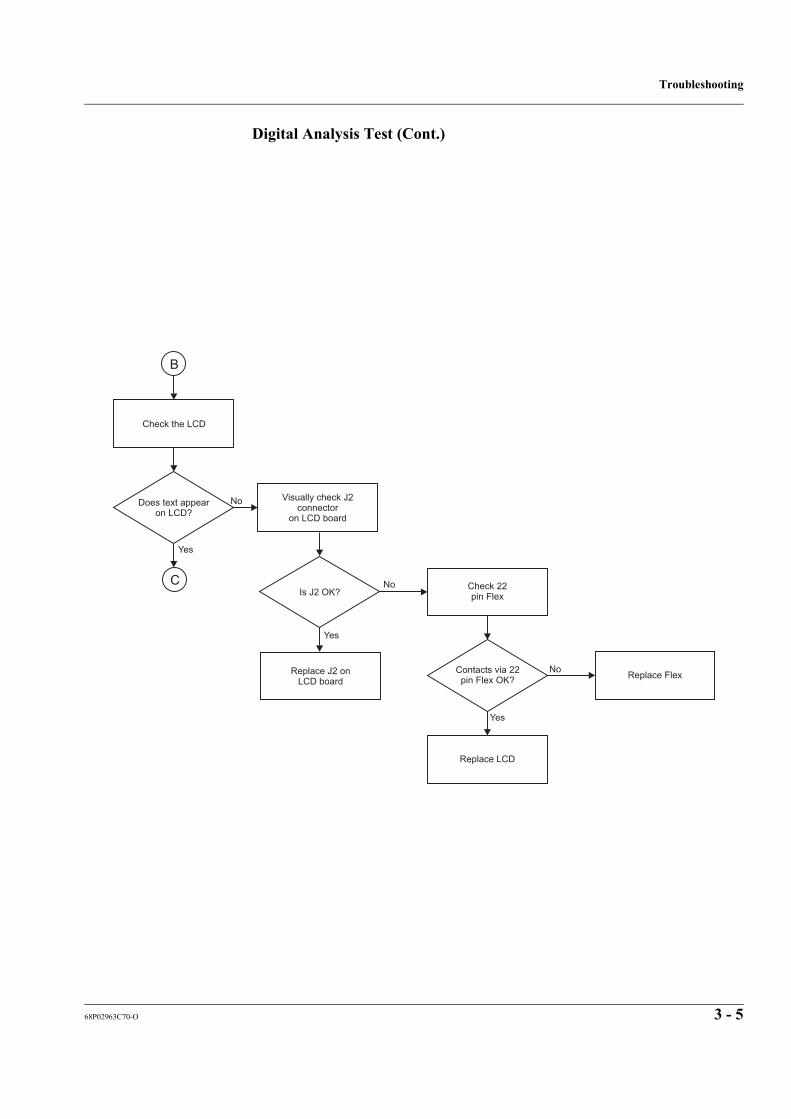
Troubleshooting
68P02963C70-O 3 - 5
Digital Analysis Test (Cont.)
Does text appearon LCD?
Is J2 OK?
Contacts via 22pin Flex OK?
Visually check J2connector
on LCD board
Check 22pin Flex
Replace LCD
Replace FlexReplace J2 onLCD board
Check the LCD
C
B
No
No
Yes
Yes
Yes
No

Troubleshooting
3 - 6 68P02963C70-O
Digital Analysis Test (Cont.)
Did thevibratorvibrate?
Is theVoltage
OK?
Are theVoltages
OK?
Check the Power SupplyV1, 1.875V on C611
when “VIBR EN” TetraComcommand has been entered
Check 1.875V on D001and <0.4V on Q002
pin 1, 4
Replace the Vibrator
Check for defectiveQ002 or D001
The Main Boardsuccessfully passed
all tests
Refer to theDC distribution (V2_2.775V)
Test flowchart
Test the vibrator
No
No
Yes
Yes
Yes
Note:This test will be perform by TetraCom SW application.Command: <VIBR EN/DIS>.
C

Troubleshooting
68P02963C70-O 3 - 7
DC Distribution (V2_2.775V) Test
Use this test on a unit with the following symptoms: no power, no V2_2.775V, V1_1.875V,V3_2.775V, VREF1_2.775V, VREF2_2.775V.
Note: The following are the DC power distribution voltages with their correct values and ap-propriate location to check the voltages:• Fused_B+ (3.6 Vdc) @ F600• Filt_B+ (3.6 Vdc) @ C640• V1_1.875V (1.875 Vdc) @ C611• V2_2.775V (2.775 Vdc) @ C610, C613, C657• V3_2.775V (2.775 Vdc) @ C609, C658, C659• VREF1_2.775V (2.775 Vdc) @ C628• VREF2_2.775V (2.775 Vdc) @ C612, C660, C661• V4_2.775V (2.775 Vdc) @ C625, C644, C647• VSIM1 (3 Vdc) @ C653• 5V_RF (5 Vdc) @ C615, C651• PWM2_1.8V (1.8 Vdc) @ C624, C648• PWM1_5.6V (5.6 Vdc) @ C623

Troubleshooting
3 - 8 68P02963C70-O
DC Distribution (V2_2.775V) Test (Cont.)
Is the voltage OK?
Is the voltage OK?
Is the voltage OK?
Is the voltage OK?
Is resistance OK?
Check the benchPower Supply
Replace FuseF600
Check junction ofF600 and VR601
for 0 (ground)�
Check traces to Fused_B+for oepens.
Check Q600 pin 4circuitry for shorts.
Repair, as necessary.
Replace E600
Check junction ofF600 and Vr601 pin 2for 3.6Vdc (Fused_B+)
Check Q600 pin 3for 3.6 Vdc
Check all Fused_B+circuit components.
Repair, as necessary.
Check C640for 3.6 Vdc (Filt_B+)
Checkbattery contact P1-4
for 3.6 Vdc
A
No
No
No
No
Yes
Yes
Yes
No
Yes
Yes

Troubleshooting
68P02963C70-O 3 - 9
DC Distribution (V2_2.775V) Test (Cont.)
Is the voltage OK?
Are frequencyand amplitude OK?
Is Resethigh?
Replace U600 (GCAP III)
ReplaceU600 (GCAP III)
Check TP600 for32 kHz clock with 2.775V
amplitude
Check TP603for the Reset high
Check Filt_B+ atC640 or C652
for 3.6 Vdc
B
A
No
No
Yes
Yes
Yes
No

Troubleshooting
3 - 10 68P02963C70-O
DC Distribution (V2_2.775V) Test (Cont.)
Is the voltage OK? Replace U600 (GCAP III)
Check C610, C613, C657for 2.775 Vdc(V2_2.775V)
Refer to otherDC DistributionTest Flowcharts
B
No
Yes

Troubleshooting
68P02963C70-O 3 - 11
DC Distribution (SWB+) Test
Use this test on a unit with the following symptoms: no SWB+.
Note: This test will be performed using TetraCom SW application commands <SWBEN/Dis>.
Is the voltage OK?Is the voltage
0.3V?<
Are voltages OK?
Is the voltage OK?
TetraComcommand“SWB Dis”
SWB+current limit
test OK
TetraCom command“SWB EN”
Check R119
Refer to theDC distribution (V2-2.775 V)
Test flowchart
Check If U104 pin 5 isshorted to ground.
Repair, as necessary.
Check U104 pin 3Voltages >2.0V for “SWB EN”
<0.4V for “SWB Dis”(SPICS4A-Redcap)
Check U104.Replace if necessary
Check U104 pin 1for 3.6 Vdc (Filt_B+)
Check U104 pin 6for 3.6 Vdc
NoNo
No
No
Yes
Yes
Yes
Yes

Troubleshooting
3 - 12 68P02963C70-O
DC Distribution (V4_2.775V) Test
Use this test on a unit with the following symptoms: no V4_2.775V.
Is the voltage OK?
Is the voltage OK?
Is the voltage OK?
Is the voltage OK?
Check tracesto the RX section,
Freq. Gen. section,and TX section
Refer to theDC distribution (V2-2.775 V)
Test flowchart
Replace U600(GCAP III)
Replace E200
Check Q602 pin 1
for 3.0 Vdcreference voltage
�
(V4DRV)
Check Q602,replace if required
Check Q602 pin 3for 3.6 Vdc(Filt_B+)
Check Q602 pin 2for 2.775 Vdc
No
No
No
No
Yes
Yes
Yes
Yes

Troubleshooting
68P02963C70-O 3 - 13
DC Distribution (V3_2.775V/PWM2_1.8V) Test
Use this test on a unit with the following symptoms: no V3_2.775V, no PWM2_1.8V.
Is the voltage OK?
Is the voltage OK?
Check C624for 1.88 Vdc
(PWM2_1.8V)
Check E401 ferritebeads by REDCAP2
for opens
Check C609, C658, C659for 2.7 Vdc
(V3_2.775 V)
Yes
No
No
Yes
Refer to theDC distribution (V2_2.775 V)
Test flowchart
Refer to theDC distribution (V2_2.775 V)
Test flowchart

Troubleshooting
3 - 14 68P02963C70-O
DC Distribution (V5_RF/PWM1/VSIM1 _5.6V) Test and (VSIM1) Test
Use these tests on a unit with the following symptoms: no V5_RF, no PWM1_5.6V,or no VSIM1_5.6V.
Is the voltage OK?
ageIs the volt OK?
Is the voltage OK?
Is the voltage OK?
Check E201for opening
Refer to theDC distribution (V2_2.775 V)
Test flowchart
Replace L600
Replace U600(GCAP III)
Disconnect E201
Check3.6 VdcL600, C601
for
Check C623for 5.6 Vdc
Check C615, C651for 5 Vdc
No
No
No
No
Yes
Yes
Yes
Yes
Refer to theDC distribution (V2_2.775 V)
Test flowchart
Check VSIMI C652for 3.0 Vdc
Is the voltage OK ?Check trace tillC24, C406, C403
Yes
Check U601 pin 3for 2.775 Vdc
No
Is the voltage OK?
Refer to theDC distribution (V2_2.775 V)
Test flowchart
Check U601 pin 1for 5.6 Vdc
Is the voltage OK?Refer to the
DC Distribution 5V-RFTest flowchart
Replace L601
VSIMI
No
Yes
Yes
No
PWMI
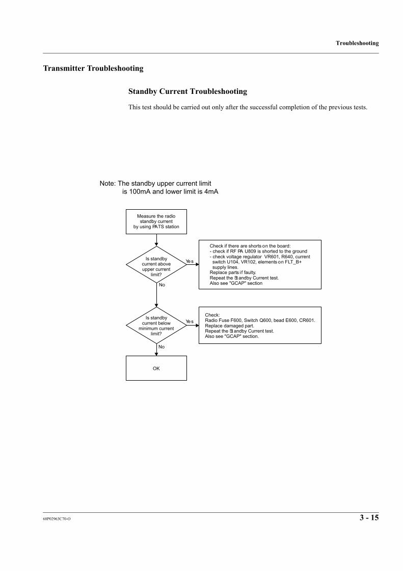
Troubleshooting
68P02963C70-O 3 - 15
Transmitter Troubleshooting
Standby Current Troubleshooting
This test should be carried out only after the successful completion of the previous tests.
Measure the radiostandby current
by using PATS station
Is standbycurrent aboveupper current
limit?
No
No
Yes
Yes
Check if there are shorts on the board:- check if RF PA U809 is shorted to the ground- check voltage regulator VR601, R640, current
U104, VR102, elements on FLT_B+supply lines.
Replace parts i f faulty.Repeat the St andby Current test.Also see "GCAP" section
switch
Is standbycurrent below
minimum currentlimit?
Check:Radio Fuse F600, Switch Q600, bead E600, CR601.Replace damaged part.Repeat the St andby Current test.Also see "GCAP" section.
OK
Note: The standby upper current limit is 100mA and lower limit is 4mA

Troubleshooting
3 - 16 68P02963C70-O
Open Loop Power Test
This test should be carried out only after the successful completion of the previous tests.
A
No
No
No
No
No
No
Yes
Yes
Yes
Yes
Yes
Yes
Measure theOpen Loop power
by using PATS
Is theoutput power
less than120mW (20.8dBm)?
Is theoutput power
above 0.5W (27dBm) ?Is the radio
in oscillation?
Check the bias voltageson pins 8,16 of RF PA U809.
Check resistors R827and R828, regulators Q807and Q911, replace partsif faulty.
Perform the Open looppower test again
Check RF PA U809, Isolator FL801, Coupler U806,components: E801, E808, E809, L916, L917, L920, L921,L923, L918, L919, C1030,C1028,C1029, C822,C867.
Replace damaged parts.Perform the Open loop power test again.
OK
Are voltages2.775V_RF, 5V_RF,
RAW_B+_RF and 2.5V_TXsupplied to the Transmitter
components?
Check the battery,regulators Q800, Q805,Q806, Q807, Q911,elements on 2.5V_TX lines.
Replace if faulty.Perform the Open loop
power test again.
Is there~ 2.5Vdc of ANT_ENsignal on Q806 pin(or C830) during
Tx slot?
Check E810.Perform REDCAP2 test.Repeat Open Loop
Power Test.
Using a Power Probe, measureRF power at the RF PAU809 input (pin 6).
Is power < -20 dBm?
Using a Power Probe test TXline-up (starting from RFPA U809 output: pins 12,13)by measuring output powerafter every component ofTransmitter till Antenna.It should be as specifiedin the spread sheet, otherwisereplace the damagedcomponents.Perform the Open loop powertest again.
Using a Power Probe,measure RF power at theLNODCT U803 outputs(pins 51,52).

Troubleshooting
68P02963C70-O 3 - 17
Open Loop Power Test (Cont.)
A
B
No
No
No
No
Yes
Yes
Yes
Yes
Is power < -4 dBm?
Check Tx line-up fromLNODCT U803 output till RFPA U809 input, replacedamaged parts.Perform the Open loop powertest again.
Perform the following:1. Visually check all components and solder connections around LN ODCT.2. Check L926 and ODCT pins 34,40,53,63 for 2.775Vdc_ODCT, check
pins 51, 52 for 5Vdc during Tx slot; check ODCT pins 45,46,56,57 for 2.3Vdcduring Tx slot.
Are all checks OK?
Replace damaged components.Perform the Open loop powertuning and test again.
Using aeasure
the RF level atpin 6 of Mixer (U800)
power highimpedance probe m
Is thepower < -6.5 dBm?
No
Yes
Check the power at pin 1of U800 mixer.
Is thesignal at U800
pin 1 stable and its power1 dBm?>
Check L809, C844.Perform Offset VCO test.Perform the Open loop powertest again.
Check the power at pin 3of U800 mixer
Is thesignal at U800
pin 3 stable and itspower -0.5 dBm?>
Replace the mixer U800.Perform the Open loop powertest again.
Check C800, L800, R805,C833.Perform Main VCO Buffer test.Perform the Open loop powertest again.
Measure the RF power at inputand output of Image filter (FL800).Calculate the difference betweenImage filter input and output.
No
Yes
Is thedifference > 3.5 dB?
Check FL800, Q808 (LO Driver),replace if faulty.Perform the Open loop powertest again.

Troubleshooting
3 - 18 68P02963C70-O
Open Loop Power Test (Cont.)
B
No
No
No
Yes
Yes
Yes
No
No
Yes
Yes
Measure the RF power at theinput of LO Driver (Q808) andinput of I/Q splitter U801.Calculate the LO Driver Gain.
Is the Gain< 22 dBm?
Check for 2.5Vdc during Tx slot,if voltage is OK, check L813, ifL813 is OK replace Q808.If there is no voltage, checkQ805 and L811.Replace damaged parts.Perform the Open loop powertest again.
Measure the RF power at inputand output of I/Q splitter (U801).Calculate the differencebetween I/Q splitter input and output.
Is thedifference > 3.5 dB?
Check I/Q splitter U801, C851,C849.Replace faulty parts.Perform the Open loop powertest again.
Measure theASW level on pin 28
of LNODCT U803 duringTx slot by using scope. Does theASW level go low (about 0V dc)
during Tx slot?
Replace LNODCT U803Perform the Open looppower test again
Replace LNODCT U803.Perform the Open loop powertest again.
Perform "WPIC Test"Perform the Open looppower test again
Was anydata detected?
Verify by using scope that there is an inputdata on pins 58-61 of the LNODCT U803.(AC voltage 300-400mV peak)
Does thetwo condition exist?
Verify by using scope that:1. There is 2.4MHz clock (1.8 0.3Vdc) on
pins 11,12 of U803 during Tx slot.2. SLT and SLTB go low on pins 9,10 of U803.

Troubleshooting
68P02963C70-O 3 - 19
WPIC Test
This test should be started in accordance to Open Loop Power test.
No
Yes
No
No
Yes
Yes
Perform the following:1. Set the unit to the Open loop test at a frequency of 390MHz.2. Read the value of WPIC1 9 register by using TetraCom. It has 8 b its.
Change the hexadecimal value of WPIC1 9 t o switch the 5-th bit from 0 to 1.3. U bserve output data voltage on Test Points 500,501.sing a scope o
Is datavoltage (0.4-0.8Vp-p)
observed duringTx slot?
Replace WPIC U503.If the Open Loop Power problemexists replace LNODCT U803.Repeat the Open Loop power test.
TetraCom Commands:WPIC 1 9Read the register value
Measure:1. 2.775_WPIC dc voltage on C572 (C516, C519, C555,
C552, C549, C573, C547, C535, C502, C542.2. V3_2.775V on C515.
Are voltages(2.6-2.9Vdc)
OK?
Perform the GCAP test.If the problem still existsreplace WPIC U503.
Measure TXE signal(0.5-2.3Vdc) during Tx slot on R514.
Is the TXE signal OK?
Verify the REDCAP2 U401 functionality,replace if faulty, repeat WPIC test, if theproblem still exists replace WPIC U503.

Troubleshooting
3 - 20 68P02963C70-O
Closed Loop Power Test
This test should be carried out only after the successful completion of the previous tests.
No
Yes
No
No
Yes
Yes
Tune the radio on PATS.
Is theradio close loop
output power <28dBmor >31 dBm?
OK
OK
Check the elements: coupler U806, R815, R818,R825, R826, C817. Replace if faulty and repeat theClose Loop test.
Does theclose loop power
problem stillexists?
Measure the LO power on pin 24 MVCOof the LNODCT U803 (800-400 mVp-p(single ended) swing into a 50Ohm load).
Is the LO power OK?
Replace LNODCT, performOpen Loop Power test andClose Loop Power test.
Check R838, C814 replace if faulty, repeatClose Loop Power test. If the problem stillexists replace LNODCT U803 and repeatOpen Loop Power test and Close LoopPower test.

Troubleshooting
68P02963C70-O 3 - 21
Transmitter Current Consumption Test
This test should be carried out only after the successful completion of the previous tests.
No
Yes
NoYes
OK
Start TX current test.
Is TXcurrent > 2.2A
(average TX current?)
1. Measure RF PA bias voltages on pins 8and 16 of U809.
2. Measure supply votage on pin 12 of U809.
Are supplyor (and) bias voltages
high?
Repeat Open loop power test andClose loop power test.If the problem still exists replace U809.Repeat Transmitter current consumption test.
1. Check power supplies;2. Repeat tuning of the radio.Repeat Transmitter currentconsumption test.

Troubleshooting
3 - 22 68P02963C70-O
Receiver Troubleshooting
No
No
No
No
No
Ye s
Ye s
Ye s
Ye s
Ye s
Is thegain below
4dB?
Is theGain still below
4db?
Is theGain still below
4db?
Check with all powerInput s/Output s o f Ant. SW .,Front Filter (Fl500), LN A(U500), Second Filter (Fl501),Mixer (U504), Xt al Filter(Fl502). Replace if necessary .Check Front Gain again.
Check second LO .-16dBm<Power<-10dBmFreq.=219.3MHzRe pa ir if necessary(See Synth. Troubleshooting)
OK
Wa s that theproblem ?
Check 2.775V suppl y t oLN A & Mixer and checkcontrol lones (Q504, Q500).Rep air if necessary .Check Front Gain again.
Check Main Synth. Powerlevel (>-5dBm) and frequency .F F +109.65MHz).Rep ai r i f necessary .(See Synth. Troubleshooting)
main = rx
TetraCom Commands (TD MMode):>Freq. RX 390.0125>Mode RXTDM/Mode RSSI>LIMITER ON>BERRout WPIC BaseBand signalto test point s:>WPI C 2 0 7 2 NOWActivating control lines atcontinuos mode:WPI C 3 9 1 b NOW
Run RX_BER -112dBm &ULTIMA TE_BER
Check BaseBand Output atWPIC (U503) TP500/TP501.
Passed?Return to firsttest.
Check Front Gain, usinga R F probe on C536,
Frequency 109.65MHz
Replace if necessary.

Troubleshooting
68P02963C70-O 3 - 23
Synthesizer Troubleshooting
Use this test on a unit with the following symptom: no Tx or Rx
Using a 50-ohm probe on thespectrum analyzer,check the LO
output at the buffer output atR927 and R944.
Is the frequencyat 503.65MHz?
Is the bufferoutput between-5 and -3dBm ?
The unit tested successfully
check the VCOoutput at R937 ,Is
the freq 529.65MHz?
Test the VCO controlvoltage at R917.The typical
range is 0.5 to 4.5 V.
Check for opens,shorts,ormissing components in the
buffer circuits.Also check for 2.3 Vdc on
L907.
Is the controlvoltage railed to<0.5V or >4.5V
Possible prescaler feedbackproblem:1.check solderin ofC933,C915.2.Probe to determine if LOis reaching the prescalerinput.
NO
YES
YES
NO
YES
Note:This isthe abnormal
condition.
No
A
NO
YES
TetraCom Commands:
MAIN_VCO ONWPIC 3 1 c0 NOWWPIC 2 4 17 NOWWPIC 2 5 F4 NOWWPIC 2 6 9e NOWWPIC 2 7 79 NOWWPIC 0 5 30 NOWWPIC 0 8 0 NOW

Troubleshooting
3 - 24 68P02963C70-O
Synthesizer Troubleshooting (Cont.)
Possible VCO problem:Check for opens orshorts in the VCO circuit.
A
Whether theproblem found
and fixed ?
Check for the following:2.4Vdc on R934 and on R923.Confirm that the resonator tabis prperly soldered.Confirm that the Varicap is inthe right direction.
Unit testingis complete
Yes
Check Loop filter:Check for opens
or shorts .
NO
Whether theproblem found
and fixed ?
Unit testingis complete
Yes
NO Check buffer:Check for opens
or shorts .
Whether theproblem found
and fixed ?
Unit testingis complete
NO
Yes
WPIC Problem

Troubleshooting
68P02963C70-O 3 - 25
Second LO VCO Test
Perform the following:1.Remove the 2nd_LO shield.2.Set the Unit to continuous
Recieve mode (Rxndc).3.Measure the 2nd_LO control
voltage at C761.
Measure the RF power level atC959 at 219.3MHz.
The 2nd_LO VCO/synthesizeris O.K.
Chek for feedbackproblem:1.check soldering ofC262,R951,C970.2.Measure the RF powerlevel at Pin 5 of the LMXat 219.3MHz.
Check Q905,R939 for solderingproblems and forthe right values.
(compare with BOM)
No
Check DC supply for the VCO:1.Check for SF_OUT on C902,R939,R906.2.Check for TETRA_2nd_LO_En onQ910.
Check DC BlockNo
Check DC supply for the LMX:1.Check for 5V_RF on C954or on Pin 22 of the LMX.2.Check 2.775V_RF on Pin
23 and Pin 24 of the LMX.
Yes
Check DC BlockNo
Perform VCO_ONLY TEST:1.connect an external 0.5 to 4.5Vpower supply to R9016.2.Measure the RF freq at C959.3.Adjust the external supply voltageuntil the frequency is219.3MHz.
The VCO is working properly.the problem is with the LMX.
Replace the LMX.
Yes
Check R915,C903,C948,R916,D902,C960,L905,C940,C920,R909,R906,C922,C921,R922,R939,R906,C953,C959 for soldering
problems andcompare with BOM
values.
No
Is the control Voltage at R916 andC948
between 0.5 and 4.5Vdc
Is the power level at 0dBm
and stable on frequency.
No
Does the VCO hasits DC Supply?
Does the LMX has itsDC Supply?
Can the frequencybe set to
219.3MHz?
Yes
Yes
TetraCom Commands:
WPIC 3 9 1b NOWdual RF 0202a2 004447
Yes
Yes
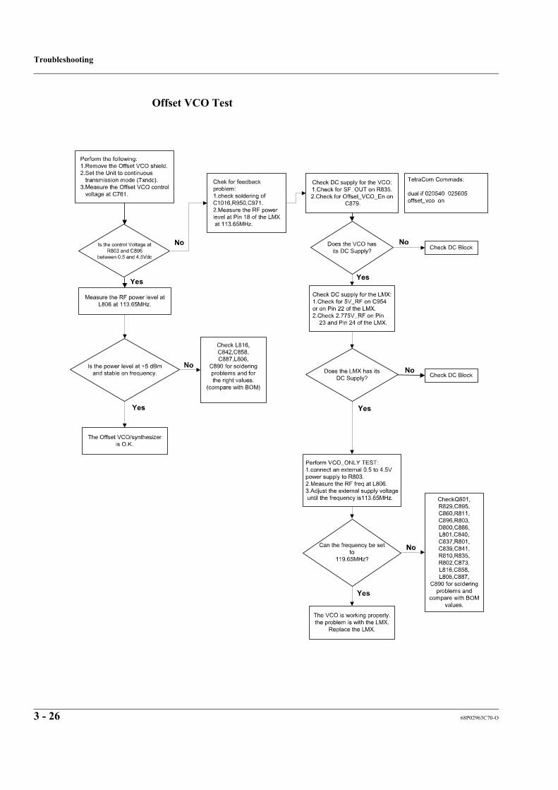
Troubleshooting
3 - 26 68P02963C70-O
Offset VCO Test

Troubleshooting
68P02963C70-O 3 - 27
Audio Troubleshooting (External Mic to External Out)
Set the audio input to the external mic to 1.02KHz @ 44mV RMS. Test sequence is controlled by TetraCom commands tothe external mic-to-external out loopback.
Check R110, C103 & continuity to connec-tor.
Check R108, C104 & continuity to connec-tor.
No trouble found
Connect a scope or DVM to the following points and measure ac levels in Vrms.
Start AUDIO_LOOPBACK (1)
Is voltage atC103 =
44mVRMS?
Yes
No
Yes
No
Tetracom Routine
MIC VAMICGA 0DSP_LOOP ONDSP_VOL 0Vol 0SPKR VA
Is voltage atC104=
66mVRMS?

Troubleshooting
3 - 28 68P02963C70-O
This page left blank intentionally

68P02963C70-O 4 - 1
Programming the Radio
Programming The Radio
1. Verify that the radio is turned off.
2. Run the Customer Programming Software (CPS) on your computer.
Codeplug Programming
1. On the menu bar, click “File” “Open”.
2. Browse for the required Codeplug file and open the file.
3. The CodePlug window appears on the screen.
4. Click the Toolbar “Tools” icon and select “Write Entire Codeplug”.
5. Press the “Yes” icon.
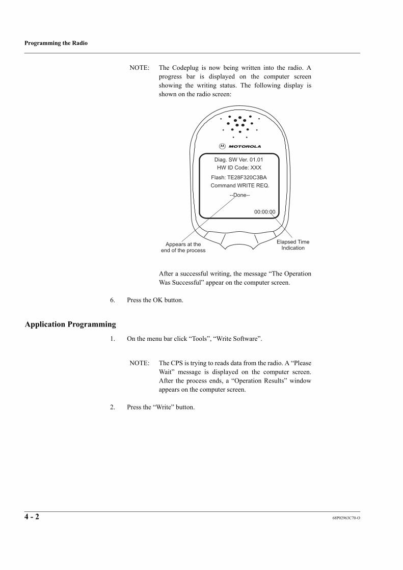
Programming the Radio
4 - 2 68P02963C70-O
NOTE: The Codeplug is now being written into the radio. Aprogress bar is displayed on the computer screenshowing the writing status. The following display isshown on the radio screen:
After a successful writing, the message “The OperationWas Successful” appear on the computer screen.
6. Press the OK button.
Application Programming
1. On the menu bar click “Tools”, “Write Software”.
NOTE: The CPS is trying to reads data from the radio. A “PleaseWait” message is displayed on the computer screen.After the process ends, a “Operation Results” windowappears on the computer screen.
2. Press the “Write” button.
Diag. SW Ver. 01.01
HW ID Code: XXX
Flash: TE28F320C3BA
Command WRITE REQ.
00:00:00
--Done--
Elapsed TimeIndication
Appears at theend of the process

Programming the Radio
68P02963C70-O 4 - 3
NOTE: The application is now being written into the radio. Aprogress bar is displayed on the computer screenshowing the writing status. The following display isshown on the radio screen:
After a successful writing, the message “The OperationWas Successful” appear on the computer screen.
3. Press the “Ok” button.
4. Click the toolbar “R” (Reset) icon.
Diag. SW Ver. 01.01
HW ID Code: XXX
Flash: TE28F320C3BA
Command WRITE REQ.
00:00:00
--Done--
Elapsed TimeIndication
Appears at theend of the process

Programming the Radio
4 - 4 68P02963C70-O
This page left blank intentionally
68P02963C70-O 5 - 1
Preventive Maintenance
This portable radio does not require a scheduled preventive maintenance program. However,periodic visual inspection is recommended.
Inspection
Inspect the radio’s external surfaces. A detailed inspection of interior circuitry is not neededor recommended.
Cleaning
The following procedures describe the recommended cleaning agents and methods to be used when cleaning the external and internal surfaces of the radio. External surfaces should becleaned whenever a periodic visual inspection reveals the presence of smudges, compound,or grime. Internal surfaces (circuit boards and components) should be cleaned only when theradio is disassembled for servicing or repair.
The only recommended agent for cleaning external radio surfaces is a 0.5% solution (one tea-spoon of detergent per gallon or four litres of water) of mild dishwashing detergent in water.The internal surfaces should be cleaned only with isopropyl alcohol (70% by volume).
Maintenance

Maintenance
5 - 2 68P02963C70-O
Safe Handling of CMOS Devices
Complementary metal-oxide semiconductor (CMOS) devices are used in the radio. While theattributes of CMOS devices are many, their characteristics make them susceptible to damageby electrostatic or high voltage charges. Damage can be latent, resulting in failure occurringweeks or months later. Therefore, special precautions must be taken to prevent device damageduring disassembly, troubleshooting, and repair. The following handling precautions aremandatory for CMOS circuits, and are especially important in low humidity conditions.
• All CMOS devices must be stored or transported in conductive material so that all ex-posed leads are shorted together. CMOS devices must not be inserted into conventionalplastic “snow” or plastic trays of the type that are used for storage or transportation ofother semiconductor devices.
• All CMOS devices must be placed on a grounded bench surface and the technician mustalso be grounded before handling the devices. This is done most effectively by havingthe technician wear a conductive wrist strap in series with a 100k� resistor to ground.
• Do not wear nylon clothing while handling CMOS circuits.
• Do not insert or remove CMOS devices with power applied. Check all power suppliesto be used for testing CMOS devices and be certain there are no voltage transientspresent.
• When straightening CMOS device leads, provide ground straps for the apparatus used.
• When soldering, use a grounded soldering iron.
• All power must be turned off in a system before printed circuit boards containing CMOSdevices are inserted, removed, or soldered.
Disassembling and Reassembling the MTH500 Unit
Mechanical checks and self tests should be performed on the unit at the basic level of service.To perform testing at the field level, it is sometimes necessary to remove the antenna and thehousing from the unit. Procedures for disassembling and reassembling the unit are describedin the sections that follow.
NOTE: Read each procedure thoroughly before performing the actual task.

Maintenance
68P02963C70-O 5 - 3
Protecting Static-Sensitive Devices
This unit contains static-sensitive devices that must be protected when opening the unit, orstoring and transporting any printed-circuit board.
To create a proper ground:• Ground the working surface of your service bench.
If possible, use the Motorola Static Protection Assembly (part #0180386A82) to groundyour service bench. This assembly contains a wrist strap, two ground cords, a table mat,and a floor mat.
• Wear a conductive wrist strap in series with a 1Mg ohm resistor to ground.
• Do not wear nylon clothing when handling any printed-circuit board.
• Prior to touching any printed-circuit board, touch an electrical ground to remove anystatic charge that might have accumulated.
To store or transport a circuit board:• Place the printed-circuit board in conductive, anti-static material.
• Do not insert the printed-circuit board into conventional plastic “snow” trays used fortransporting other devices.

Maintenance
5 - 4 68P02963C70-O
Removing and Installing the Antenna
The antenna must be removed each time the back housing is removed.
Recommended tools: no tools are required
To remove the antenna from the unit:(See Figure 13)
• Unscrew the antenna counter clockwise until it is detached from the handset.
To install the antenna in the unit:• Screw the antenna clockwise to the handset.
Figure 13 Antenna Removal and Installation
Removing and Installing Battery Door and Battery
Recommended tools: no tools are required
To remove the battery door from the unit:(See Figure 14)
1. Place the unit facing down on the work area.

Maintenance
68P02963C70-O 5 - 5
2. Press the battery door release button, slide the door towards the bottom of the unit and lift it up from the unit.
Figure 14 Battery Door Removal
To remove the battery:(See Figure 15)
1. Press the battery fastening bridge toward the upper side of the unit.
2. Simultaneously, using other hand, release the battery from its chamber.
Figure 15 Battery Removal

Maintenance
5 - 6 68P02963C70-O
To install the battery:
1. Locate the battery so that the lower part (coloured silver) is touching the lower wall of the battery chamber.
2. Carefully press the battery down until it snaps into location.
To install the battery door:
1. Position the door on the unit over the battery so that the door release button is just above the battery fastening bridge.
2. Slide the door upward until the door snaps into location.
3. Verify that the door is aligned with the handset back housing.
Removing and Installing the Back Housing
Recommended tools: T-8 Torx bit, Torx driver, mini flat-tip screwdriver
Removing the back housing from the unit:(See Figure 16)
1. Remove the antenna, refer to “Removing and Installing the Antenna”.
2. Remove the battery door and the battery, refer to “Removing and Installing Battery Door and Battery”.
3. Place the unit facing down on the work area.
4. Using the screwdriver remove the oval label at the top of the unit and the tamper evi-dent label in the center to enable access to all six screws fastening the back housing. Clean the adhesive remains of the tamper evident label using alcohol.
5. Using the Torx driver with the T-8 Torx bit, unscrew the six screws fastening the back housing.
6. Carefully remove the back housing from the unit.

Maintenance
68P02963C70-O 5 - 7
Installing the back housing:
1. Position the back housing over the unit.
2. Verify that the cover is positioned correctly, screw holes are aligned to the threads of the front housing, external antenna connector is inserted into its dedicated hole, and the styling groove of the back housing meets the styling groove of the front housing.
3. Set the Torx driver to 3.5 in-lb (0.4 Nm).
4. Screw the back housing screws in the following order: Upper left and right screws, center left and right screws and lower left and right screws.
5. Glue a new oval label over the holes of the two upper screws and a new tamper evident label (*only available to Motorola Services Centres) on the holes of the two center screws.
6. Install the battery and the battery door, refer to “Removing and Installing Battery Door and Battery”.
7. Install the antenna, refer to “Removing and Installing the Antenna”.
Figure 16 Back Housing Removal and Installation
Oval Label
External Antenna Connector
Back HousingFastening Screws
(X6)

Maintenance
5 - 8 68P02963C70-O
Removing and Installing the Vibrator
Recommended tools: mini flat-tip screwdriver
Removing the vibrator:(See Figure 17)
1. Remove the back housing, refer to “Removing and Installing the Back Housing”.
2. Turn the back housing up side down and, using the screwdriver, remove the vibrator from its chamber inside the back housing.
Installing the vibrator:
1. Carefully push the vibrator into its chamber in the back housing.
2. Install the back housing, refer to “Removing and Installing the Back Housing”.
Figure 17 Vibrator Removal and Installation
Back Housing
Vibrator

Maintenance
68P02963C70-O 5 - 9
Removing and Installing the Main Board
Recommended tools: no tools are required
Removing the main board from the unit:(See Figure 18)
1. Remove the back housing, refer to “Removing and Installing the Back Housing”.
2. Gently lift the main board, I/O connector side at the bottom of the board first, and re-move it from the unit.
3. Gently remove the rubber seal from the I/O connector, verify that the seal is not dam-aged (retain the seal for reinstallation).
Installing the main board:
1. Gently install the rubber seal over the I/O connector.
2. Position the main board in location. Verify that the two guide pins are inserted into the holes in the main board.
3. Gently push the main board down and verify that the Board-to-Board connector is properly connected to the keypad board.
4. Verify that the I/O rubber seal is properly located in the unit.
5. Install the back housing, refer to “Removing and Installing the Back Housing”.
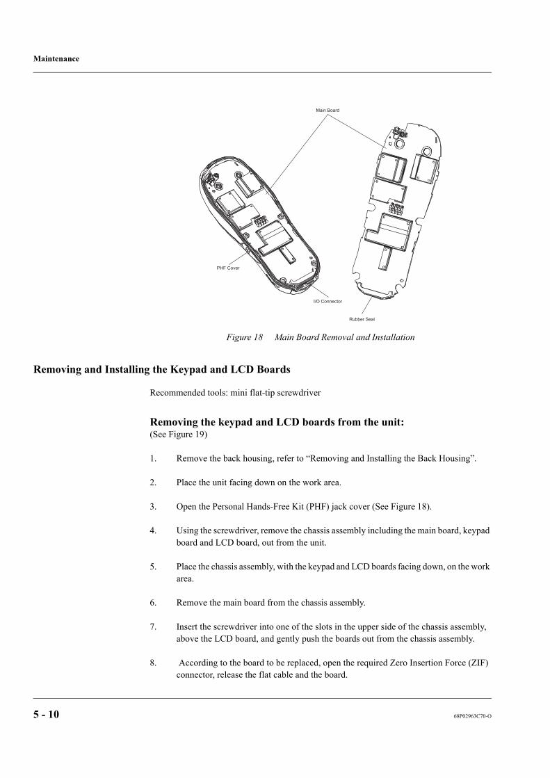
Maintenance
5 - 10 68P02963C70-O
Figure 18 Main Board Removal and Installation
Removing and Installing the Keypad and LCD Boards
Recommended tools: mini flat-tip screwdriver
Removing the keypad and LCD boards from the unit:(See Figure 19)
1. Remove the back housing, refer to “Removing and Installing the Back Housing”.
2. Place the unit facing down on the work area.
3. Open the Personal Hands-Free Kit (PHF) jack cover (See Figure 18).
4. Using the screwdriver, remove the chassis assembly including the main board, keypad board and LCD board, out from the unit.
5. Place the chassis assembly, with the keypad and LCD boards facing down, on the work area.
6. Remove the main board from the chassis assembly.
7. Insert the screwdriver into one of the slots in the upper side of the chassis assembly, above the LCD board, and gently push the boards out from the chassis assembly.
8. According to the board to be replaced, open the required Zero Insertion Force (ZIF) connector, release the flat cable and the board.
Main Board
PHF Cover
I/O Connector
Rubber Seal

Maintenance
68P02963C70-O 5 - 11
Installing the keypad and LCD boards:
1. Place the keypad and LCD boards on the work area so that the ZIF connectors are fac-ing up.
CAUTION: Care must be taken when installing the keypad and LCD boards on the chassis.Failure to comply may result in tear of the flat cable between the two boards.
2. Insert the flat cable into the ZIF connectors and close the connectors doors until a click is heard.
3. Insert the LCD board between the two snags at the sides of the chassis assembly.
4. Push the LCD board down until it snaps into location.
5. Verify that the chassis center guide pin is properly located inside the hole in the LCD board and that the snag at the top of the chassis is inserted into the slot of the board.
6. Install the keypad board on the chassis assembly.
7. Verify that the keypad board is sited parallel to the chassis assembly.
8. Verify that the main board is fully installed with the rubber seal.
9. Turn the chassis assembly up side down.
10. Install the main board on the chassis assembly. Verify that the two guide pins are in-serted to the holes in the main board.
11. Verify that the guide pins are properly located and that the Board-to-Board connector is properly connected to the main board.
12. Install the chassis assembly with the boards into the unit. Verify that the I/O connector rubber seal is properly located in the unit.
13. Install the back housing, refer to “Removing and Installing the Back Housing”.

Maintenance
5 - 12 68P02963C70-O
Figure 19 Keypad and LCD Boards Removal and Installation
Removing and Installing the LCD Module Assembly
Recommended tools: no tools are required
To remove the LCD module assembly from the unit:(See Figure 20)
1. Remove the LCD board, refer to “Removing and Installing the Keypad and LCD Boards”
NOTE: Do not touch the LCD module assembly in the active viewing area;fingerprints on this surface cannot be easily removed.
2. Using your hand, gently disengage the right two snaps and rotate the LCD module as-sembly to the left until it disengaged from the LCD board.
Chassis Assembly
LCD BoardRelease Slot
LCD Board
Keypad Board
ZIF Connectors
Board-to-BoardConnector
Flat Cable

Maintenance
68P02963C70-O 5 - 13
To install the LCD module assembly:
NOTE: Do not touch the LCD module assembly in the active viewing area;fingerprints on this surface cannot be easily removed.
1. Locate the LCD module above the LCD board so that the two guide pins are aligned with the holes in the LCD board.
2. Gently push the module down, right snaps first and then left snaps.
3. Verify that the snaps are located correctly inside the board slots.
4. Remove the protective film from the LCD glass. Verify that no damage exists on the LCD glass.
5. Install the LCD board, refer to “Removing and Installing the Keypad and LCD Boards”.
Figure 20 LCD Module Removal and Installation
LCD Board
LCD Module
LCD ModuleSnaps(X4)
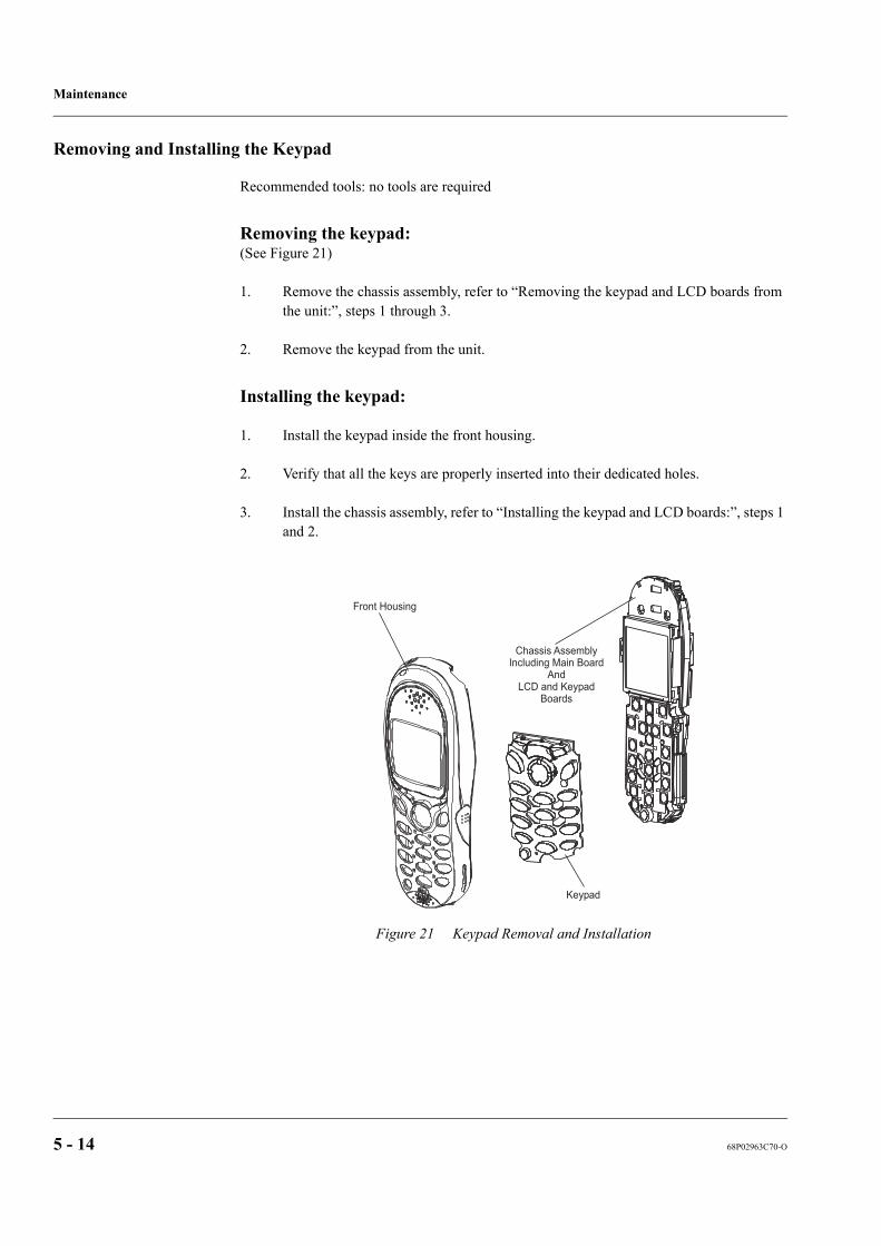
Maintenance
5 - 14 68P02963C70-O
Removing and Installing the Keypad
Recommended tools: no tools are required
Removing the keypad:(See Figure 21)
1. Remove the chassis assembly, refer to “Removing the keypad and LCD boards from the unit:”, steps 1 through 3.
2. Remove the keypad from the unit.
Installing the keypad:
1. Install the keypad inside the front housing.
2. Verify that all the keys are properly inserted into their dedicated holes.
3. Install the chassis assembly, refer to “Installing the keypad and LCD boards:”, steps 1 and 2.
Figure 21 Keypad Removal and Installation
Front Housing
Chassis AssemblyIncluding Main Board
AndLCD and Keypad
Boards
Keypad

Maintenance
68P02963C70-O 5 - 15
Removing and Installing the Microphone
Recommended tools: no tools are required
Removing the microphone:(See Figure 22)
1. Remove the chassis assembly, refer to “Removing the keypad and LCD boards from the unit:”, steps 1 through 3.
2. Remove the microphone.
Installing the microphone:
1. Insert a microphone into location.
2. Install the chassis assembly, refer to “Installing the keypad and LCD boards:”, steps 1 and 2.
Removing and Installing the Earphone
Recommended tools: mini flat-tip screwdriver
Removing the earphone:(See Figure 22)
1. Remove the Acoustic Safety Rubber.
2. Remove the chassis assembly, refer to “Removing the keypad and LCD boards from the unit:”, steps 1 through 3.
3. Using the screwdriver, remove the earphone from the unit. If the earphone was de-tached from its bottom plate, remove the plate as well.
Installing the earphone:
1. Install the Acoustic Safety Rubber.
2. Using the screwdriver, remove the protective film from the adhesive layer at the ear-phone bottom plate.
3. Insert the earphone into location. Verify that the two snags at the earphone sides are properly located in their dedicated slots.
4. Gently push the earphone until it is firmly glued inside the front housing.

Maintenance
5 - 16 68P02963C70-O
5. Install the chassis assembly, refer to “Installing the keypad and LCD boards:”, steps 1 and 2.
Figure 22 Microphone and Earphone Removal and InstallationMicrophone
Earphone
Acoustic Safety Rubber
Front Housing
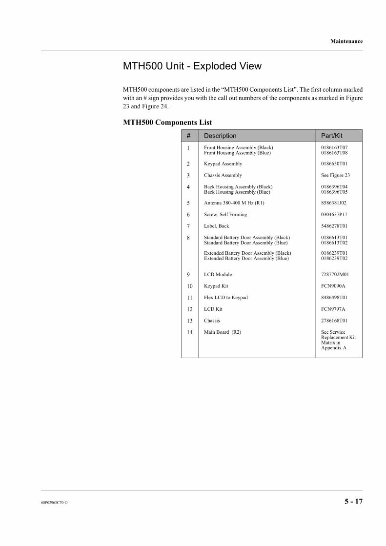
Maintenance
68P02963C70-O 5 - 17
MTH500 Unit - Exploded View
MTH500 components are listed in the “MTH500 Components List”. The first column markedwith an # sign provides you with the call out numbers of the components as marked in Figure23 and Figure 24.
MTH500 Components List
# Description Part/Kit
1 Front Housing Assembly (Black)Front Housing Assembly (Blue)
0186163T070186163T08
2 Keypad Assembly 0186630T01
3 Chassis Assembly See Figure 23
4 Back Housing Assembly (Black)Back Housing Assembly (Blue)
0186396T040186396T05
5 Antenna 380-400 M Hz (R1) 8586381J02
6 Screw, Self Forming 0304637P17
7 Label, Back 5486278T01
8 Standard Battery Door Assembly (Black)Standard Battery Door Assembly (Blue)
Extended Battery Door Assembly (Black)Extended Battery Door Assembly (Blue)
0186613T010186613T02
0186239T010186239T02
9 LCD Module 7287702M01
10 Keypad Kit FCN9090A
11 Flex LCD to Keypad 8486498T01
12 LCD Kit FCN9797A
13 Chassis 2786168T01
14 Main Board (R2) See Service Replacement Kit Matrix in Appendix A

Maintenance
5 - 18 68P02963C70-O
Figure 23 Exploded View
1
2
3
4
5
7
6 (X6)
8

Maintenance
68P02963C70-O 5 - 19
Figure 24 Exploded View of Chassis Assembly
9
12
13
10
11
14

Maintenance
5 - 20 68P02963C70-O

MTH500 Detailed Service Manual - COMPONENT BOARD LAYOUTS
68P02963C70-O 6 - 1
Component Board Layouts

MTH500 Detailed Service Manual - COMPONENT BOARD LAYOUTS
6 - 2 68P02963C70-O
This page intentionally left blank

MTH500 Detailed Service Manual - COMPONENT BOARD LAYOUTS
68P02963C70-O 6 - 3
Keypad Board (FCN9090A) - Sides 1 and 2
8487639U01_P1
OL 79B02964C13-O
SHOWN FROM SIDE 1O1 79B02964C11-O
P1
C1
C2
C3C4
C7
C8
C9
C10
C11
C12
E1
J1
P2
R1R2
R3
R4R5
R6
TP
1
TP
2T
P3
TP4
U1
U2
U3
U4
U5
VR1
VR2
VR3
VR
4
1
1
1
11 1
1
11
1
1
1
O1 79B02964C12-OSHOWN FROM SIDE 2
OL 79B02964C14-O
8487639U01_P1
D1
D2
D3
D5
D6
D7
D8
D9D10D
13
D14
D17
MK1
S1
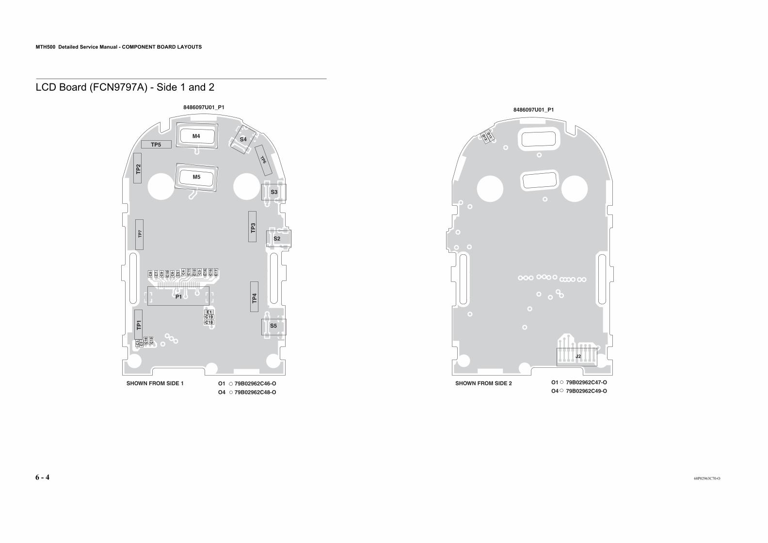
MTH500 Detailed Service Manual - COMPONENT BOARD LAYOUTS
6 - 4 68P02963C70-O
LCD Board (FCN9797A) - Side 1 and 2
O4 79B02962C48-O
SHOWN FROM SIDE 1 O1 79B02962C46-O
8486097U01_P1
P1
C1
C2
C3
C4
C5
C6
C7
C8
C9
C10 C11
C12
C13
C14
C15
C16
C17
C18C19E1
M4
M5
S2
S3
S4
S5TP
1T
P2
TP
3T
P4
TP5
TP6
TP
7
8486097U01_P1
D11D
12
O1 79B02962C47-OSHOWN FROM SIDE 2O4 79B02962C49-O
J2
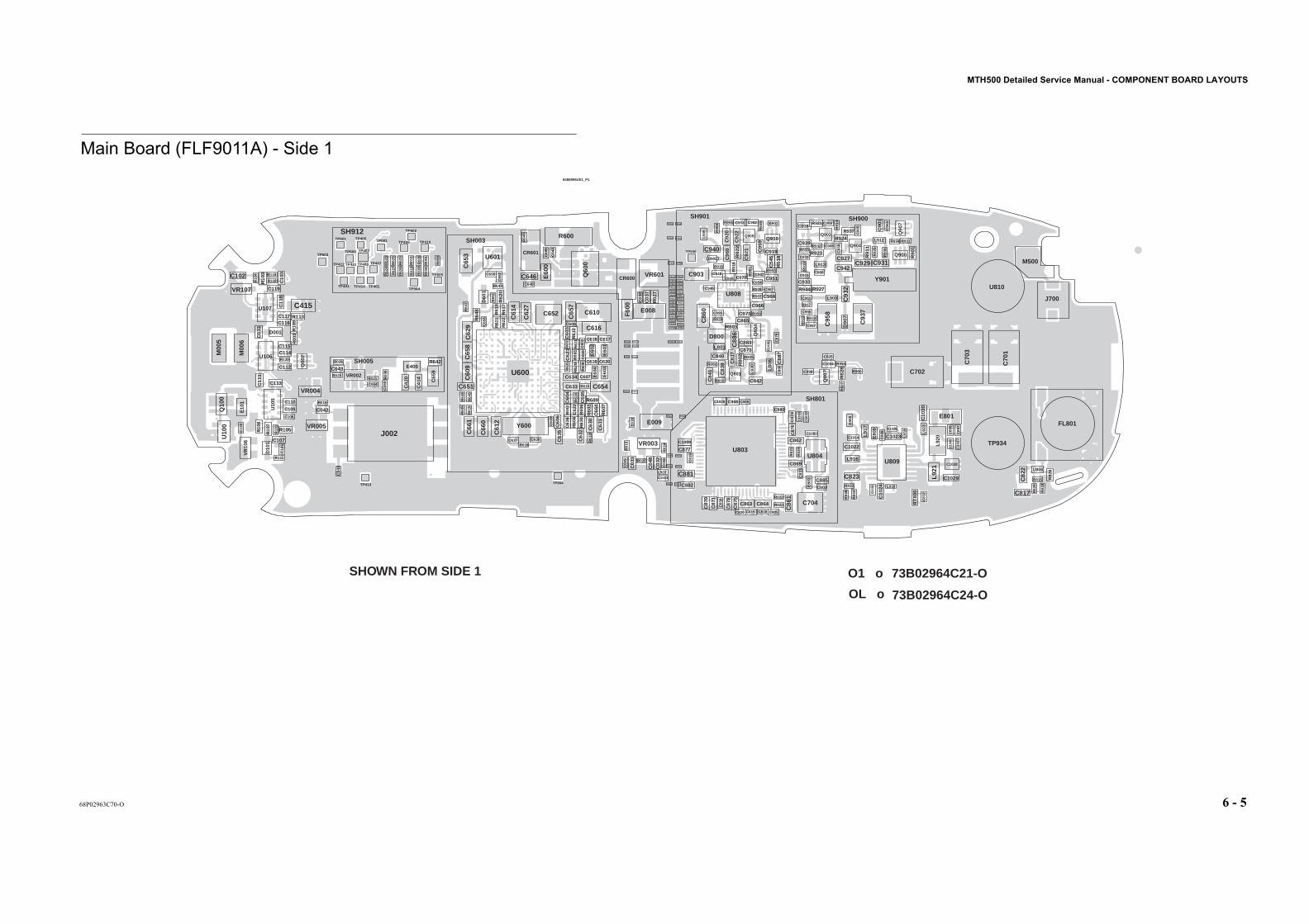
MTH500 Detailed Service Manual - COMPONENT BOARD LAYOUTS
68P02963C70-O 6 - 5
Main Board (FLF9011A) - Side 1
73B02964C24-O
73B02964C21-O
TP823TP923
TP830
TP804
TP930
TP904
TP915 TP815
TP806TP906
TP905 TP805
TP824TP924
TP917 TP817 TP802TP902
TP935 TP850
TP803TP903
TP919 TP819
TP818TP918
TP925 TP825
TP828TP928
TP922 TP822
TP821TP921
TP913 TP813
TP809TP909
TP912 TP812
TP832TP932
TP920 TP820
TP829TP929
TP933 TP833
TP808TP908
TP911 TP811
TP814
J002
Y901
D90
7
SH901
SH003SH912
J700
M500
TP914
8488996U01_P1
SHOWN FROM SIDE 1 O1 o
C03
1
C03
2
C03
3
C03
5
C03
6
C03
7C
038
C04
1
C042
C043
C044
C04
8
C05
0
C10
1C102
C10
3
C107
C108
C109
C110
C11
1
C112
C113
C114C115
C116C117
C11
8
C119
C12
0
C41
4
C415
C42
0
C54
5C60
0
C60
2C60
3C
604
C60
5
C60
6
C607
C608
C60
9
C610
C61
2
C61
4
C616
C617C618
C619 C620C62
1C
622
C62
7
C62
9
C63
0
C63
1
C63
2
C633
C634
C63
5
C63
6
C637 C638
C63
9
C640
C64
3
C646C650
C651
C652
C65
3
C654
C65
5
C65
6 C65
7
C65
8
C65
9
C66
0
C66
1
C66
2
C66
4
C70
1
C702
C70
3
C704
C802
C805
C809
C81
2
C815 C816
C817
C81
8
C820
C82
2
C823
C825
C83
1
C83
4
C83
7
C83
9
C840
C84
1
C842
C86
0
C86
1
C862
C863 C864
C865
C868
C869
C87
0C
871
C873
C87
4
C87
5
C87
6
C877
C87
8
C87
9
C880
C881
C882
C883
C885
C88
6
C88
7
C88
8
C89
0
C895
C89
7
C89
8
C899
C90
1C902
C903
C90
4
C90
5
C906
C909
C910
C915C916
C919
C92
0
C92
1
C92
2
C927C929
C93
0
C931
C93
2
C933
C93
7
C938
C939C940
C942
C946
C948C951
C953
C954
C955
C957 C95
8
C95
9
C96
0
C961
C962
C966
C967
C968
C970
C971
C980
C1004
C1009C1014
C10
16
C1020
C1022
C1023
C10
24
C10
25
C1026
C10
27
C1028
C1029
C10
30
C1031
C10
32
C10
33
C10
45
C1050
CR600
CR601
D001
D10
1
D60
1
D800
D902
E008
E009E01
0
E10
1
E400
E60
0
E60
1
E60
2
E60
3
E60
4
E801
E80
3
E80
8
E80
9
E901
F60
0
FL801
L801
L80
6
L903
L90
5
L912
L913
L916
L91
7
L918
L91
9
L92
0L
921
L922
L92
3
L93
0
M00
5
M00
6
Q00
2
Q10
0
Q60
0
Q801
Q80
4
Q80
7
Q900
Q903
Q904
Q905
Q90
7
Q910
R00
1
R00
3
R00
4
R00
8
R00
9R
010
R01
1R
012
R01
3
R01
4
R019
R020R021
R025
R026
R02
7
R10
1
R10
3
R10
4
R105R10
6
R10
7
R10
9
R110
R111
R113
R118
R120
R51
8
R600
R60
1
R60
2
R60
3
R60
4
R60
5
R60
6
R60
7
R60
8
R609
R610
R61
1R
612
R61
3
R61
4
R61
5
R616
R61
7
R61
8R
620
R62
1
R62
2
R62
3
R62
4
R62
5
R62
6
R62
7
R62
8
R62
9R
630
R63
1R
632
R64
0
R642
R643
R64
5
R64
6R
647
R64
8
R65
0
R65
1
R801 R80
2
R803
R810
R815
R81
8
R82
1
R822
R823
R82
4
R82
5
R82
6
R82
7R
828
R829
R833
R83
4
R835
R83
6
R90
1
R906
R907
R908
R90
9
R91
1
R91
3
R91
4
R915
R91
6
R917
R918
R91
9
R921
R92
2
R923
R924
R92
5
R927
R931R932
R933
R934
R93
6
R937R93
9
R944
R950
R95
1
R953
R954
R960
RT
800
SH005
SH801
SH900
TP001
TP401
TP402
TP403
TP405
TP407TP408
TP409 TP410
TP411TP412
TP413
TP414TP504
TP600
TP601
TP602
TP603
TP604
TP605
TP934
TP936
U10
0
U10
5
U106
U107
U600
U601
U803U804
U806
U808
U809
U810
VR002
VR003
VR004
VR005
VR
106
VR107
VR601
Y600
OL o

MTH500 Detailed Service Manual - COMPONENT BOARD LAYOUTS
6 - 6 68P02963C70-O
Main Board (FLF9011A) - Side 2
8488996U01_P1
E00
2
E004
E00
3
E00
6
E00
5
J10
M001
M002
P15
M501
Q808
E810
E800
E80
7
E500
E501
TP002
C00
1
C00
2C
003
C004
C00
5
C006
C007
C00
8
C00
9
C01
0C
011
C01
2
C01
3C
014
C01
5
C016C01
7
C01
9C
020
C02
1
C02
2
C02
3C
024
C02
5
C02
6
C02
7C
028
C02
9
C049
C10
4
C105
C10
6
C121
C12
2
C20
0
C20
1
C203
C204
C205
C206
C401
C402
C403
C40
4
C40
5
C40
6
C40
7
C40
8
C40
9
C41
0
C412C413
C41
6
C417
C418
C41
9
C421
C42
2C
423
C424
C425
C426
C42
7
C42
8
C42
9
C43
0
C500
C50
1
C50
2
C50
3
C504
C505
C507
C508
C510
C51
2
C513
C51
4
C515
C51
6
C518
C51
9
C52
1
C522
C524C525
C526
C52
7
C52
8
C530
C53
1
C53
2
C53
3
C534C535
C53
6
C53
9
C54
2
C54
6
C547C549
C55
0
C55
1
C552
C55
3
C554
C55
5
C557
C56
0
C56
1
C57
2
C573
C574
C576
C577
C58
0
C59
0
C60
1
C611
C613
C61
5
C623 C62
4
C625 C626
C62
8
C641
C64
2
C64
4
C647
C64
8
C649C66
3
C800
C80
8
C81
1
C814C819
C82
1
C824
C827
C828
C829 C830
C832
C83
3
C835C838
C843
C844
C84
5
C846
C847
C848
C84
9
C85
0
C85
1
C85
2
C85
3
C85
4
C855
C85
6
C857
C859
C866
C867
C891
C894
C984
C1010
C10
11
C10
12
C1015
C10
21
C10
46
C1048
C1049
CR602
CR
603
D500
D801
E00
1E007
E10
2
E201
E203
E40
1
E80
6
FL500
FL
501
FL502
FL800
L50
0
L50
1
L50
4
L505
L508L512
L51
3
L518
L519
L520
L52
5
L53
0
L60
0
L601 L602
L800
L803
L805
L80
8
L809
L810
L811
L81
2
L81
3
L81
5
L817
L818
L81
9
L89
0
L931
L932
Q500
Q504
Q602
Q80
0Q805
Q80
6
R01
5R
016
R10
8
R119
R12
1
R401
R405
R40
7
R41
7
R500
R504
R512
R514
R515
R51
7
R519
R520
R52
1
R58
0
R649
R80
0
R80
4
R805
R806
R80
7
R80
8
R80
9
R812
R81
4
R81
6
R817
R819
R82
0
R83
2
R838
R899
R943
R94
5
R95
6
R961
R962
R963
R964
R965
R966
R967
R968
RT500
SH500
SH501
SH502
SH802
SH911
TP500
TP501 TP502
TP503
U104
U401
U402
U403
U40
5
U50
0U503
U504
U80
0
U80
1
U802
VR101
VR
102
VR104
VR105
Y501
SHOWN FROM SIDE 2
73B02964C24-O
73B02964C22-OO1 o
OL o

MTH500 Detailed Service Manual - Schematic Diagrams and Parts Lists
68P02963C70-O 6 - 7
Schematic Diagrams and Parts Lists

SCHEMATIC DIAGRAMS - MTH500 Keypad Board (FCN9090A)
6 - 8 68P02963C70-O
MTH500 Keypad Board (FCN9090A)
INT_EAR+_R
GREEN LED
GND contact
pinsGND
RESET
Connector GND pins
BACKLIGHT-
RESET
1
9
MK12
1+
VALUEC8
INT_EAR-_R
ON_OFF
PTT
ROW4
COL2
COL4
PHF_GND
PHF_MIC
PHF_SENSE
PHF_PTT
PHF_EAR
PHF_JACK
place close to
ROW2
ROW1
MENU
UP
GND
GND
GND
GND
GND
GND
FLEX to Display Board
BACKLIGHT-
RESET
CHIP SELECT
2.775_DISPLAY
RS
DATA
CLOCK
INT_EAR+
INT_EAR-_PHF_EAR
PHF
ON_OFF
PTT
GND
INT_MIC+
INT_MIC-
ROW1
ROW2
COL0
COL1
COL2
COL3
COL4
SEND/ENDSOFT KEY
LEFT
SOFT KEY
RIGHTDOWN MODE
* 7
80
4
5
1
2
369#
MUTE LEFT
40 pin Main To Keypad conn
RED LED
RIGHT
ROW0
BACKLIGHT+
GREEN LED
ROW3
ROW4
COL0
COL1
COL2
COL3
COL4
PHF_GND
GND
PHF_MIC
GND
GND
GND
GND
GND
GND
PHF_SENSE
GND
GND
INT_MIC+
INT_MIC-
CHIP SELECT
2.775_DISPLAY
RS
DATA
CLOCK
MIC
ROW0
BACKLIGHT+
RED LED
ROW3
ROW4
R3
68
J1-5
J1-3
J1-4
5GN
D1
1
GN
D2
6
R110
R29
R38
R47
U5
FLTR_EZAST33A
C12
C23
C34
C4
1G
ND
1
6G
ND
2
10R1
9R2
8R3
7R4FLTR_EZAST33A
U3
2C1
3C2
4C3
C45
P2-22
22
P2-9
7
P2-19
19
P2-1
1
P2-7
2
P2-3
3
P2-4
4
P2-2
5C4
1G
ND
1
6G
ND
2
10R1
9R2
8R3
7R4
FLTR_EZAST33A
U4
2C1
3C2
4C3
VALUE
C9
41
P1-42
42
38
P1-41
P1-37
37
P1-38
35
P1-36
36
P2-5
5
P1-35
10
P2-8
8
P2-11
11
P2-10
18
P2-17
17
P2-21
21
P2-18
P2-20
20
VR4VR3
VR1 VR2
0.
R6
R5 0.
0.R4
VALUE
C4
VALUE
C3
C2
VALUE
C1 33.u
5
P1-4
4
P1-6
6
P1-5
P1-11
J1-1
J1-2
N2
S1
A1 A2
Q1 Q2
S1
N1
S1
V1 V2
S1
T2
S1
U1 U2
9R2
8R3
7R4
S1
T1
2C1
3C2
C34
5C4
6G
ND
1G
ND
21
10R1
P2-24
24
U2
EZAST21
P2-23
23
C34
C45
GN
D1
1
GN
D2
6
R110
R29
R38
R47
U1
FLTR_EZAST33A
C12
C23
E1
BLM11B601S
C12
10.n1.u 180.p
C11
S1
X1 X2
C10S1
M1 M2W1 W2
S1
G1 G2
11
S1
P1-40
40
P1-11
26
P1-39
39
P1-25
25
P1-26
23
P1-24
24
P1-22
22
P1-23
20
P1-21
21
18
P1-20
2
P1-17
17
P1-18
15
P1-2
P1-16
16
P1-15
P2-15
15
P2-16
16
6
P2-14
14
13
P2-6
P2-12
12
P2-13
C7
VALUE
P1-19
19
BACKLIGHT+
BACKLIGHT+
14
P1-13
13
P1-12
12
P1-14
9
P1-7
7
P1-10
10
P1-9
3
P1-8
8
S1 S2
P1-3
L2
S1
R1 R2
S1
K1 K2
S1
L1
S1
J1 J2
S1
P2
S1
H1 H2
E1 E2
S1
P1
S1
D1 D2
S1
B2
S1
C1 C2
F1 F2
S1
B1
P1-34
34
S1
32
P1-33
33
P1-31
31
P1-32
29
P1-30
30
28
P1-29
P1-27
27
P1-28

MTH500 Detailed Service Manual - MTH500 Keypad Board (FCN9090A) Component Parts
68P02963C70-O 6 - 9
MTH500 Keypad Board (FCN9090A) Component Parts
When ordering component parts, the part number should be included.
CAPACITORS CONNECTOR and INDUCTORS RESISTORS
Ref # Part # Description Ref # Part # Description Ref # Part # Description
C1 2311049A30 Tant. chip 33µF J1 0985885K01 conn.J
C2 9186929J02 400&880MHz resonance Cap.
P1 0986926J03 conn.J
C3 9186929J02 Part not placed P2 0986966J01 conn.J INTEGRATED CIRCUITS
C4 9186929J02 400&880MHz resonance Cap.
C7-9 9186929J02 Part not placed GENERAL Ref # Part # Description
C10 2113743P01 Part not placed Ref # Part # Description U1 9186133U02 FLTR_EZAST33A
C11 2113928A01 1µF U2 9185759B01 EZAST21
C12 2113741F49 10nF MK1 5086346J02 Part not placed U3-5 9186133U02 FLTR_EZAST33A
DIODES RESISTOR
Ref # Part # Description Ref # Part # Description ZENER DIODES
R1-2 0662057C43 res_47 Ohm Ref # Part # Description
LED R3 0662057A21 res_68 Ohm VR1-4 4804645P09 Suppr. 6V
Ref # Part # Description R4-5 0662057A18 res_51 Ohm
D1 4886955J02 Part not placed R6 0662057B47 res_0 Ohm
D2-3 4886955J02 LED_grn S1 9997639U01 Keypad_22
D5 4886955J02 LED_grn
D6 4886955J02 Part not placed
D7-10 4886955J02 LED_grn
D13-14 4886955J02 LED_grn
D17 4886955J02 LED_grn
E1 2409134J04 BLM11B6016

SCHEMATIC DIAGRAMS - MTH500 LCD Board (FCN9797A)
6 - 10 68P02963C70-O
MTH500 LCD Board (FCN9797A)
RS
2.775_DISPLAY
CHIP SELECT
DNP DNP
73D02964C07-O
DNP DNP
BACKLIGHT+
BACKLIGHT-
RESET
CLOCK
DATA
DNPDNP DNP DNPDNP
RED LED
GREEN LED
INT_EAR+_R
INT_EAR-_R
ON_OFF
PTT
ROW4
COL2
COL4
GND
GND
FLEX to Keypad Board
2.775_DISPLAY
RS
CHIP SELECT
GND
GND
GND
BACKLIGHT+
BACKLIGHT-
RESET
DNP DNPDNPDNPDNPDNP
DNP DNP DNP DNP DNP
VOL DOWN
VOL UP
ON/OFF
PTT
ROW4
COL2
COL4
RED GREEN
GROUND CONTACTS
DNP DNPDNPDNP
DISPLAY
GND
CLOCK
DATA
C3
180.p
C2
180.p
P1-14
14
C1
180.p
P1-4
4
P1-1
1
P1-22
22
P1-16
16
P1-21
21
P1-20
20
18
P1-19
19
M4
P1-18
4A
J2-5A5A
J2-7A7A
J2-4A
2A
J2-1A1A
J2-6A6A
J2-2A
8A
J2-3A3A
J2-9A9A
J2-8A
BACKLIGHT+
BACKLIGHT+
BACKLIGHT+
C12
180.p 180.p
C11
180.p
C10 C9
180.p 180.p
C8 C7
180.p
P1-15
15
C6
180.p
12
P1-13
13
5
P1-6
6
P1-12
3
P1-2
2
P1-5
8
P1-7
7
P1-3
P1-9
9
P1-8
P1-10
10
P1-17
17
M5
P1-11
11
J2-5B
C16
180.p
J2-4B
J2-9B
J2-7B
TP7CLIP
CLIP1
CLIP1
TP6CLIP
CLIP1
TP4CLIP
CLIP1
TP5CLIP
CLIP1
TP3CLIP
CLIP1
TL
SU
1008
_RE
D
D12
TP2CLIP
TL
GU
1008
_GR
N
D11
3
A24
B1 1
B2 2
B2 2
S2
A1
S5
A13
A24
B1 1
S4
A13
A24
B1 1
B2 2
S3
A13
4 A2
B1 1
B2 2
J2-8B
J2-3B
J2-6B
J2-1B
J2-2B
180.p
C5
180.p
TP1CLIP
CLIP1
C4
10.n
C19
1.u
C18
BLM11B601SE1
24
180.p
C17
P1-23
23
P1-24
C15
180.p
C14
180.p180.p
C13

MTH500 Detailed Service Manual - MTH500 LCD Board (FCN9797A) Component Parts
68P02963C70-O 6 - 11
MTH500 LCD Board (FCN9797A) Component Parts
When ordering component parts, the part number should be included.
CAPACITORS RECEPTOR RESISTORS
Ref # Part # Description Ref # Part # Description Ref # Part # Description
C1-17 2113743p01 Part not placed
C18 2113928A01 1µF GENERAL
C19 2113741F49 10nF Ref # Part # Description INTEGRATED CIRCUIT - AUDIO
M4-5 3986295T01 Contact Ref # Part # Description
S2-5 4086218A02 Switch
TP1-7 4209080u02 Part not placed
DIODES RESISTOR
Ref # Part # Description Ref # Part # Description
LED
Ref # Part # Description
D11 4886955j02 LED_grn
D12 4886955j01 LED_red
CONNECTOR and INDUCTORS
Ref # Part # Description
E1 2409134j04 Ind. chip fer.
J2 0988189K02 conn_J
P1 0986966j01 conn_J

SCHEMATIC DIAGRAMS - MTH500 MAIN Board (FLF9011A)
6 - 12 68P02963C70-O
MTH500 MAIN Board (FLF9011A)
5V_RF
ANT_EN
LO_Driver_En
LO_Mixer_En
PA_Bias
PA_TEMP
RAW_B+_RF
RESET
16.8_MHz_CLK
RF
79B02964C09-O
SHEET 1 OF 9
SPIA_CS2_ODCT
SPIA_MISO
SPIA_MOSI
SYNTH_CS
TCXO_WARP
TETRA_MAIN_VCO_ON
V3_2.775
V4_2.775V_RF
VREF1_2.775V
WPIC_OSC_EN
WPIC_SRD
WPIC_SSI_FSYNCH
WPIC_STD
WPIC_TXCLK
WPIC_TXE
DIGITAL
WPIC_STD
WPIC_TXCLK
WPIC_TXE
16.8_OR13_MHz_CLK
5V_RF
ANT_EN
LO_Driver_EN
LO_Mixer_EN
PA_BIAS
PA_TEMP
RAW_B+_RF
RESET
RF_TEMP
RX_ACQ
SPIA_CLK
SPIA_CS0_WPIC
RF_TEMP
RX_ACQ
SPIA_CLK
SPIA_CS0_WPIC
SPIA_CS2_ODCT
SPIA_MISO
SPIA_MOSI
SYNT_CS_
TCXO_WARP
TETRA_MAIN_VCO_ON
V3_2.775V
V4_2.775V
VREF1_2.775V
WPIC_FSYNC
WPIC_OSC_EN
WPIC_SRD

MTH500 Detailed Service Manual - MTH500 Main RF Block
68P02963C70-O 6 - 13
MTH500 Main RF Block
SHEET 2 OF 9
VA Connector
N/U
N/U N/U
N/U
N/U
1
TP828
CHTSTP
1
79B02964C09-O
Digital Test Point Shield
Antenna Contacts
C205
270.p
VALUE
TP825
CHTSTP
L931
1.u
E201
CHTSTP
1
TP808
CHTSTP
1
TP817
CHTSTP
1
TP804
CHTSTP
1
TP811
CHTSTP
1
TP823
CHTSTP
1
TP824
CHTSTP
1
TP815
CHTSTP
1
TP818
CHTSTP
1
TP821
1
TP805
CHTSTP
1
TP806
CHTSTP
1
TP830
CHTSTP
1
TP819
CHTSTP
1
TP822
CHTSTP
C1046
47.0U
M500
SHIELD
SH912
1
M501
TP934
1
GND
PLATED_HOLE5_2X7_6
U810
1
GND
J700-4
4
PLATED_HOLE5_2X7_6
1
J700-3
3
J700-2
2
J700-1
PA_BIAS
PA_TEMP
RAW_B+_RF
RX_TETRA
SPI_CLK
SPI_MISO
SPI_MOSI
TCLK
TCLKB
TETEA_TX_LO TETRA_ANT
TSLOT
TSLOTB
VCNTO
offset_vco
2.775V_RF
5V_RF+
ANT_EN
ASW
GND
LO_Driver_EN
LO_Mixer_EN
ODCT_CS
OD
CT
_RE
SE
T
OUTI
OUTIB
OUTQ
OUTQB
C206
CHTSTP
TP802
100.n
100.n
C204
C201
100.n
270.p
C200
C203
270.p
RX_2nd_LO
SF_OUT
SPIA_CLK
SPIA_CS3_SYNT
SPIA_MOSI
TETRA_2nd_LO_Enable
TETRA_MAIN_VCO_ON
TETRA_RX_LO
TETRA_TX_LO
offset_vco
offset_vco_En
TSLOT
TSLOTB
TXCLK
TXE
V3
VCNTO
VREF1_2.775V
WPIC_CE
WPIC_RESET
2.775V_RF
5V_RF+
ADAPT
CPGITR
Ded_Synt_Ref
GND
PRSCINPRSCIN
RF_TEMP
RX_2nd_LO
RX_ACQ
RX_TETRA
SF_OUT
SPI_CLK
SPI_IN
SRD
SSI_FSYNCH
STD
TCLK
TCLKB
TCXO_WARP
TETRA_2nd_LO_Enable
TETRA_RX_LO
2.775V_RF
5V_RF+
ADAPT
ASW
CLK_OUT
CPGITR
Ded_Synt_Ref
GND
OSC_EN
OUTI
OUTIB
OUTQ
OUTQB
E203
VALUE
CHTSTP
TP850
TP833
CHTSTP
1
TP812
CHTSTP
1
CHTSTP
TP809
1
CHTSTP
TP813
1
TP829
CHTSTP
1
TP814
CHTSTP
1
CHTSTP
1
TP803
CHTSTP
1
832
CHTSTP
1
RF_TEMP
16.8_OR13_MHz_CLK
SPIA_CS0_WPIC
WPIC_TXE
WPIC_STD
WPIC_SSI_FSYNCH
WPIC_TXCLK
WPIC_SRD
RX_ACQ
WPIC_OSC_EN
TP820
LO_Mixer_EN
PA_TEMP
V4_2.775V_RF
5V_RF
V3_2.775
ANT_EN
VREF1_2.775V
TCXO_WARP
RESET
SYNTH_CS
TETRA_MAIN_VCO_ON
LO_Driver_EN
SPIA_CS2_ODCT
PA_BIAS
RAW_B+_RF
SPIA_MISO
SPIA_CLK
SPIA_MOSI
ReceiverTETRA Transmitter
Frequency Generation

SCHEMATIC DIAGRAMS - MTH500 Transmitter Block (Sheet 1 of 2) )
6 - 14 68P02963C70-O
MTH500 Transmitter Block (Sheet 1 of 2) )
6.8n6.8n 6.8n
CMY210
DG0106A01
380Mhz
300300
18
1.8p
8V
DD
VC
C
49USUB
ODCT_H19GED
U803
23VSSR
17V
OF
F
6SPISB
5SPIO
4
14V
CP
53V
CC
U
22V
CC
O34
VC
CD
63V
CC
2
40
RFOUTB52
RFOUT
36RFINB
37RFIN
20
30TST4
29TST3
27TST2
26TST1
2
13LSUB
47LP2QB
48LP2Q
54
SPII
3SPIC
10SLTB
9SLT
51
LP1IB44
LP1I
45LOQB
46LOQ
56
OVCOB
19OVCO
25MVCOB
24MVCO
MRSTB
GN
DU
21G
ND
O35
GN
DD
62G
ND
2
39
LP2IB55
LP2I
41LP1QB
42LP1Q
43
2.775V_RF
CAPR
32CAPO
31CAPM
58BINQB
R824
18
59BINQ
L1T0
L1T1(LO Line Up)
ODCT Shield
ODCT Bottom Shield
60BINIB
61BINI
6.8n
1
2
N/U
N/U
N/U N/U
N/U N/U
N/U
6.8n N/U
28ASW
GN
D
15G
CP
33DSUB
7D
GN
D
16CPO
12CLKIB
11CLKI
1CAPRB
64
LOIB
57LOI
38LCAP
2.5V_TX
C850
4.3p
390.p
18G
OF
F
50
18.0n
18
R823
C862
R82118
GND GND GND
GND
GND
270.p
C805
5V_RF+
6.8NF
C880
C812
270.p
C874
100.n 100.n 100.n
C870
GND
GND
2.775V_ODCT
GNDGND
C868
270.p
C802
GND GND
C809
GND
270.p
R806
1.2K
GND
R812
270
100n100n
L805
270.p
L803
R817
C81451.
51.
R816
270.p
C819
270.p
C811
270.p
GND
GND
GND
GND
C818
270.p
C820
GND
C863
C815
270.p
C816270.p
C864
GND
C882
4.7n
GND
C881
4.7nC861
18.0n
18
R822
R808
300
GND GND
300
R819
R800
18
GND
R838
150.
R833
GND
R834
51.
R836
R814
C849
2.4p
C851
3.p
39n
L807
SLC_045P
IN
ISOL
OUT_0
OUT_90
GND
U801
GND
C877
2.775V_ODCT
GND GND
C878
C871
GND GNDGND GND
2.775V_ODCT
100.n
C869
100.n
C876
100.n
C875
100.n
L811
8.2n
GND
2.775V_RF
L813
22.n
GND
15.p
C843
12.p
C845C854
1.n
GND
1.n
510 C853
R807
GND
8.2p
C847
270.p
C821
100.p
C894C844
10.p
12.p
L810C846 12n
12n
L809
L800
68nC800
82.p
U800
2G
ND
1
5G
ND
2
6IF_RF
3LO_IN
1RF_IF
4
VDD
R804 C859
GND
2.2K
GND
GND
8.2
R820
L808
22n
DS
S1
2.775V_RF
2.5V_TX
Q808
Q800
E800
BLM10B601SDP
GND GND
47K
RT800
C828
270.p
C857
1.n
C827
GND
C856
GND
270.p
C855
GND
1.n
1.n 270.p
C824
BA_IN3
1B_IN
GN
D1
2 7G
ND
2
8NC1
6U_OUT
GND
5V_RF+
GND
2.5V_TX
U804
C1033
2.775V_ODCT
GND
C1032
270.p
GND
270.p
270.p
C1031
1
GND
BLM10B601SDP
L922
1
GND
SH802
SHIELD
100.n
GND
SH801
SHIELD
6OUT
7OUT_GND
GND
C1020
1G
ND
15
GN
D2
4G
ND
38
GN
D4
2IN
3IN_GND
GND
FL800
GND
C1009
10u
C704
BLM11B601S
E806
BLM11B601S
E803
GND
56n
L815
470.p
C833
R805
560
C834
270.p
GND
C885
100.n
8.2n
L812
270.p
C1050C831
R964
2K
330
GND
R961
R963
4.7K
GND
R962
4.7K
Q805
22n
L926
GND
2.775V_RF
LO_Driver_EN
offset_vco
LO_Mixer_EN
5V_RF+
TCLKB
ASW
GND
OUTIB
SPI_CLK
SPI_MOSI
SPI_MISO
TETEA_TX_LO
2.775V_RF
OUTI
ODCT_CS
ODCT_RESET
TSLOTB
OUTQ
TCLK
TSLOT
OUTQB
PA_TEMP
10K
10K
10K10K
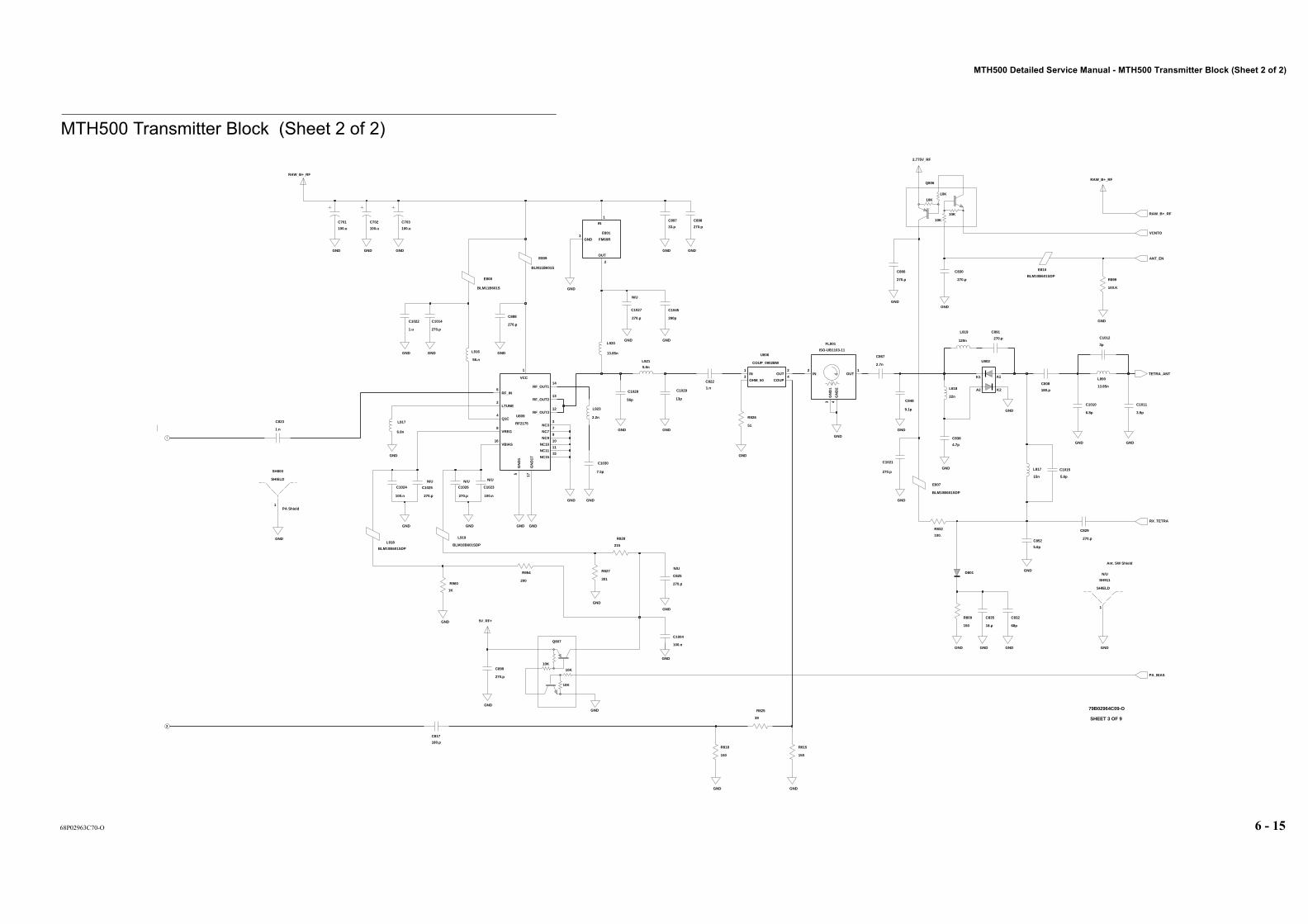
MTH500 Detailed Service Manual - MTH500 Transmitter Block (Sheet 2 of 2)
68P02963C70-O 6 - 15
MTH500 Transmitter Block (Sheet 2 of 2)
PA Shield
Ant. SW Shield
79B02964C09-O
SHEET 3 OF 9
N/U
N/U
13p
2.2n
6.8n
N/U N/U N/U
200 301
215
56p
7.5p
390p
N/U
9.1p
120n
22n
6.8p
3p
15n
4.7p
68p
5.6p
ISO-UB1103-11
GND
1OUT
GND
C822
1.n
GND
R954
C1045
1K
GND
SH911
SHIELD
1
GND
R960
C848
L923
BLM10B601SDPBLM10B601SDP
L919
GNDGND
L918
C1026
270.p270.p
C1025
100.n
C1024
GND
100.n
C1023
1.u
C1022270.p
GND
5.6n
L921
C1027
GND
13.85n
L920
GND
C1029
C1030
GND
C1028
GND
GND
56.n
L916
L917
RF_IN6
RF_OUT114
RF_OUT213
RF_OUT312
VBIAS16
VCC
1
VREG8
GND
LTUNE2
NC1010
NC1111
NC1515
NC33
NC77
NC99
Q1C4
RF2175
U809
GN
D1
5 17G
ND
17
R899
100.K
GND
GND
E810
C1021
270.p
GND
BLM10B601SDP
SH800
SHIELD
1
GND
C1015
C1014
GND
5.6p
GND GND
270.p
C1011
3.9p
C1010
13.85n
C1012
GND
L890
5V_RF+
GND
C1004
100.n
C899
270.p
Q807
GND
GND GND GND
100.u
C703C702C701
100.u
4COUP
1IN
OHM_503
2OUT
100.u
GND
COUP_0902BW
U806
C897
33.p
E808
E809
BLM11B601S
GND
BLM11B601S
GND
C832
51
R826
GND
E807
BLM10B601SDP
GND
R818
150
C835
18.p150
R809
GND
D801
L818
GND
GND
OUT
2
C867
2.7n
E801
FM60RGND3
IN
1
R832
100.
A1
A2
K1
K2
U802
Q806
GND
C891
270.p
270.p
C830
C838
GND
L819
C829
GND
270.p
C866
270.p
270.p
C825
GND
1.n
C823
GND
RAW_B+_RFRAW_B+_RF
R828
R827
270.p
GND
C898
GND
C888
2.775V_RF
270.p
FL801
GN
D1
3 4G
ND
2
2IN
180.p
C808
GND
L817
C852
180.p
C817
GND
39
R825
R815
150
ANT_EN
VCNTO
RX_TETRA
RAW_B+_RF
PA_BIAS
TETRA_ANT
10K
10K
10K
10K
10K
10K
10K
2

SCHEMATIC DIAGRAMS - MTH500 Receiver Block (Sheet 1 of 2)
6 - 16 68P02963C70-O
MTH500 Receiver Block (Sheet 1 of 2)
Enviorement Temp. Sens.
GPO5/DCLICP
should be 75n
Pins crossed for better routing
RX Front End Shield
N/U
1
2
3
4
5
6
DG0106A01
39n
47n
270p
22n
3.6p0380MHZ-BPF
N/U N/U
98A02
C524
L932
270.
R965
C1048
270.p
L530
R580
220.
C590
270.p
SH501
SHIELD
1
2.775V_WPIC
C510
270.p
C500
270.p
22n
L525
R519
R945
470470
R517
1.n
2.775V_RF
Q504
VREF1_2.775V
C513
470.p
C984
R943
560
D500
7OUT_GND
C574
270.p
1G
ND
15
GN
D2
4G
ND
38
GN
D4
2IN
3IN_GND
6OUT
FL500
E501
BLM10B601SDP
47K
RT500
E500
BLM10B601SDP
5V_RF+
V3
C514
270.p
2.775V_RF
2.775V_RF
2.775V_RF
Q500
6
GN
D1
GN
D2
2
8IN
4OUT
FL501
C576
C550
1.n
L500
L518
33n
6.8p
C521
C532
R500
1.K
C505
1n
C553
100.0n
C507
GN
D1
2
GN
D2
54
RF0UT
1RFIN
VPD3
1.n
RF2361U500
56.n
L508
12.n
L513
C528
C522
8.2p
68.n
L505
100.p
1.n
C551
VD
D4
270.p
C512
U504
GN
D1
2
GN
D2
5
IF_RF6
LO_IN3
RF_IF1
12.n
L512
CMY211
C531
12.p
C525
6
OUT4
IN1
4.7n
FL502
GN
D2 3
GN
D1
GN
D2
5
GN
D3
C539
1.8p
470.n
L504
1.8p
5V_RF+
V3
RF_TEMP
VREF1_2.775V
RX_TETRA
GND
2.775V_RF
PRSCIN
ADAPT
CPGITR
TETRA_RX_LO
10K
10K10K
10K
10K
10K
10K
10K

MTH500 Detailed Service Manual - MTH500 Receiver Block (Sheet 2 of 2)
68P02963C70-O 6 - 17
MTH500 Receiver Block (Sheet 2 of 2)
470.K
TP504
10.n
N/U
N/U
5
6
79B02964C09-O
SHEET 4 OF 9
4GPO6/DCLICIN
Tetra RX Mixer + 2nd LO Enable
3
2
1
RX IF Shield
Warp from WPIC
WPIC Shield
N/U
N/U
N/U
C516
100.n
7
8
6
5
C530
10.n
10.n
C534
VAGBYPE3
VBLINL5
VCNTOJ6
VCOCT1K1
VCOCT2J2
XTALBASEK6
XTALEMITL6
J8XTALWARP
D9TESTD_GP04
TME11
A11TSLOT
TSLOTBA10
K11TXCLK_SCK
TXE_TXKEYH8
TXKEYOUTF2
VAGE1
SRDJ11
STDK10
TCAPMC7
TCAPPB8
TCLKB11
TCLKBC10
TEST1D4
TEST2D3
SERIALGNDL8
SERIALVCCH11
K4SFBYP
SFGNDK3
L4SFOUT
SFVCCJ4
SPICLKK9
SPIIL9
REFPLLVCCG10
REFVCCB10
RFA0B1
RSTBE10
H9RXACQ
RXCLKJ10
RXFSL11
SATDETH1
PREINGBA3
PREINIB4
PREINIBA4
PRSCING1
QGNDC11
QVCCD10
REFGNDB9
REFPLLGNDH10
PLLCPF11
PLLCPVCCF9
PLLEMITG9
PRAGNDA2
PRAGNDDIGA1
C3PRAVCC1
PRAVCC2B5
PREINGB3
OUTIBA9
A8OUTQ
OUTQBC8
D6PKGGND1
F4PKGGND2
PKGGND3F8
PKGGND4H6
G11PLLBASE
MNCPGNDK2
MNCPVCCH4
NGNDD11
E9NVCC
OSCENBJ9
OSCGNDK5
OSCVCCJ7
OUTID8
J1GPO1
GPO2H2
GPO3B7
LOGICGNDL7
LOGICVCCK7
D1LOIN
G2MAINGND
MAINVCCH3
C6DCLQCIN
A6DCLQCP
DETSWJ3
DMCSL10
DMXGNDB2
DMXGNDDIGC2
DMXVCCC1
D2DMXVCCDIG
K8CEX
CLKOUTF10
C9CLKSEL
L3CPGITR
L2CPGT
CREFA7
DCLICINC5
DCLICPB6
ADAPTL1
AGCF3
AGCDRIVEG3
AGCGNDE2
AGCVCCF1
ASWJ5
BBFGNDA5
BBFVCCC4
9
9
U503
WPIC27C02
1
2
10uF
C561
100.n
C555
5
4
3
2
6
7
2.775V_WPIC
2.775V_WPIC
2.775V_WPIC
2.775V_WPIC
2.775V_WPIC
2.775V_WPIC
L519
220.n
L520
220.n
10.p
C527
C560
C526
10.p
10uF
3.3n
C542
100.n
C547
C502
100.n
100.n
C508
100.nC549
C535
100.n
C572
100.n
100.n
C501
C504
100.n
C515
100.n
100.K
R521
TP502
C580
1.n
V_CONT1
100.K
R520
Y501
TCXO_16.8MHZ
GND
2
OUTPUT
3
VCC
4
TP500
TP501
FREQ
51
R518C545
5.1p
3
4
C519
100.n
5
4
3
2
7
8
2.775V_WPIC
2.775V_WPIC
2.775V_WPIC
2.775V_WPIC
2.775V_WPIC
2.775V_WPIC
8
6
R968
22
R967
C1049
270.pR966
39
R956
0.
1
SH502
SHIELD
1.n
C552
33.
R504
100.n
C573
C554
47.n
C518
100.n
3
2
1
7
6
5
4
C533
C577
10u
VREF1_2.775V
10n
C503
R515
100K
R514
5.1K
R512
100K
1
2.775V_WPIC
5V_RF+
V3
TP503
SH500
SHIELD
C557
15n
C546
1.5p
C536
22p
470.n
L501
TCXO_WARP
8
SF_OUT
Ded_Synt_Ref
RX_ACQ
WPIC2(1:9)
SRD
SSI_FSYNCH
TETRA_2nd_LO_Enable
OSC_EN
WPIC_RESET
WPIC_CE
SPI_CLK
SPI_IN
STD
TXCLK
TXE
ASW
TCLKB
VCNTO
OUTIB
OUTI
WPIC1(1:8)
TSLOTB
TSLOT
TCLK
OUTQB
OUTQ
RX_2nd_LO
CLK_OUT

SCHEMATIC DIAGRAMS - MTH500 Frequency Block Tetra Main VCO (Sheet 1 of 2)
6 - 18 68P02963C70-O
MTH500 Frequency Block Tetra Main VCO (Sheet 1 of 2)
TETRA Main VCO
N/U
Main VCO Shield
N/U
3382022n
12p
3.6p
100n
GND
C955 D907
C937
1
GND
GND
SHIELD
SH900
10n18.pC980
L907
GND
100p
C915
C942
15p
R919510.
GND
C932
5V_RF+
GND
GND
SF_OUT
SF_OUT
2.775V_RF
Q907
GND
GND GND
GND
GND
GND GND
GND
GND
C938
1.5K
R933C939
4.3p
GND
100.p
C909
270
R921
Q903
GND
R924
R932
68
R914
1.3K
GND
3.6K
100.p
C906
51
R937
C910
GND
GND
100.p
R944
22.
R927
C933
22
5.6p
R918
180
R917
75
100n
C958
GND
R913
C957
4.7n
R911
2.2K
22.0n
C961
C929
5.1p
L903
390n
390nL913
L912
390n5.1p
C931
15.p
C927
C930
100p
100p
C905
C904 C901
270.p 100.n
R901
47.K
R925
R936
100.
R923
68.
R934
1.K
R931
8.2K
FREQ
RESONATOR
Y901
Q900
PRSCIN
TETRA_MAIN_VCO_ON
SF_OUT
2.775V_RF
5V_RF+
GND
Q904
ADAPT
CPGITR
TETRA_TX_LO
TETRA_RX_LO
10K
10K
10K
10K
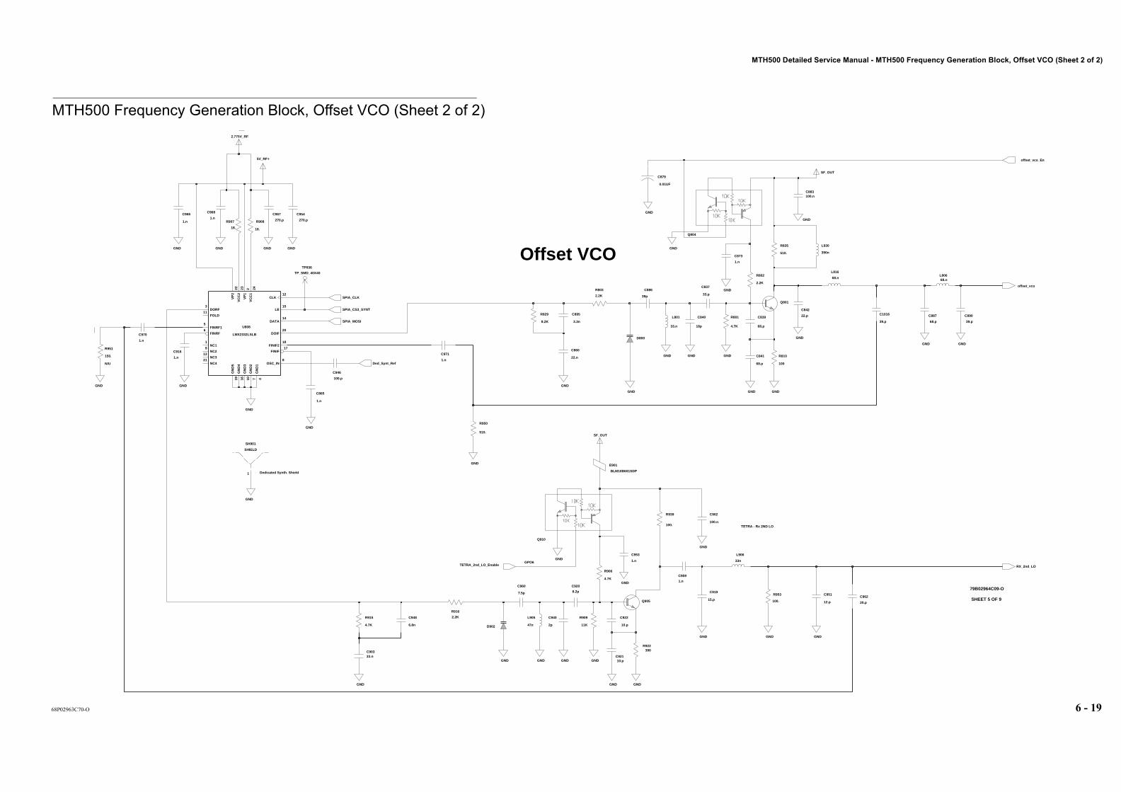
MTH500 Detailed Service Manual - MTH500 Frequency Generation Block, Offset VCO (Sheet 2 of 2)
68P02963C70-O 6 - 19
MTH500 Frequency Generation Block, Offset VCO (Sheet 2 of 2)
TETRA - Rx 2ND LO
GPO6
Offset VCO
Dedicated Synth. Shield
N/U
79B02964C09-O
SHEET 5 OF 9
39p
18p
L930
390n
GND
TP936
TP_SMD_40X40
1
GND
R953
100.
GND
SHIELD
SH901
1.n
C970
150.
R951
510.
GND
R950
C971
1.n
6.8n
39.p
C1016
GND
C948
33.nC903
R915
4.7K
1.n
C865
GND
1.n
GND
18.
GND
GND
C916
R908
18.
R9071.n
C966
NC3
NC421 8
OSC_IN
24V
CC
1
23V
CC
2
2V
P1
22V
P2
GND
GN
D1
7G
ND
210
GN
D3
16G
ND
419
GN
D5
15LE
NC11
9NC2
13
DATA
20DOIF
3DORF
17FINIF
18FINIF2
6FINRF
5FINRF1
11FOLD
4
GND
LMX2332LSLB
U808
12CLK
14
C968
GND
C9671.n
GND
SF_OUT
GND
270.p
Q804
GND
L80668.n
39.p
C890
R803
2.2K
GND
D800
68.p
C887
0.01UF
C879
GND
1.n
GND
GND
C883
GND
C873
100.n
68.n
L816
GND
GND
22.p
C842
33.n
L801
GND GND
GND
C840
C88633.p
C837
68.p
C841
68.p
C839
4.7K
R801
2.2K
R802
510.
R835
Q801
100
R810
GND
BLM10B601SDP
E901
GND
GND
100.p
C946
270.p
C954
1.n
C953
5V_RF+
GND
2.775V_RF
SF_OUT
D902
Q910
C951
12.p
C962
GNDGND
GND
GND
GND
20.p
GNDGND
GND
C902
100.n100.
R939
C940
2p
33n
L906
R922390
2.2K
R916
4.7K
8.2p
C920
11K
R906
R909
8.2K
R829 C895
3.3n
22.n
C860
C960
C959
1.n
7.5p C919
15.p
C92110.p
10.p
C922L905
47n
Q905
offset_vco_En
offset_vco
SPIA_MOSI
TETRA_2nd_LO_Enable
Ded_Synt_Ref
RX_2nd_LO
SPIA_CS3_SYNT
SPIA_CLK

SCHEMATIC DIAGRAMS - MTH500 Main Digital Block (Sheet 1 of 2)
6 - 20 68P02963C70-O
MTH500 Main Digital Block (Sheet 1 of 2)
WPIC_TXE
WPIC_DSPCLK
WPIC_FSYNC
WPIC_SRD
WPIC_STD
RX_ACQ
WPIC_OSC_EN
RAW_B+_RF
SPIA_CLK
SPIA_MOSI
SPIA_MISO
N.C. RESET TETRA
DATA TETRA
CLK TETRA
COL0
COL1
COL2
COL3
COL4
ROW0
ROW1
ROW2
ROW3
ROW4
PA_TEMP
TETRA SIM
SYNT_CS_
RF_TEMP
DATA
RESET
CLOCK
TETRA_RESET
TETRA_CLK
TETRA_DATA
TETRA_VSIMTETRA_VSIM
PTT/PHF_PTT
PHF_MIC
MIC-
MIC+
Backlight-
GRN_LED
RED_LED
ON/OFF
DATA
CLOCK
PHF_GND
GND
GND
GND
GND
GND
GND
RESET
PHF_SENSE
EARPIECE+
PHF_EAR/EARPIECE-
Backlight+
V3_2.775V
DISPLAY_RS
CHIP_SEL
MAIN TO KEYPAD
40 pin connector
COL0
COL1
COL2
COL3
COL4
ROW0
ROW1
ROW2
ROW3
ROW4
GND
GND
GND
GND
GND
SPIA_CS0_WPIC
SPIA_CS2_ODCT
PA_BIAS
LO_Mixer_EN
LO_Driver_EN
TETRA_MAIN_VCO_ON
ANT_EN
16.8_OR_13MHz_CLK
RESET
J002
Contact GND
Contact GND
1
2
3
4
5
6
7
8
9
10
11
12
13
14
13
14
15
16
17
18
19
20
21
22
23
24
25
26
27
28
29
30
31
32
33
34
35
36
37
38
39
40
41
42
46
47
44
45
43
DNP
DNP
DNP
DNPDNPDNP
DNP
DNP
DNP
DNP
DNP
DNP
DNP DNP DNP DNP DNP DNP DNP DNP DNP DNP DNP
N/U
41
P15-42 42
3
12
VSIM
P15-41
12
VR005
VR0043
R026
05
6
VREF2_2.775V
7
2
3
1
C043 C044
22p 100.p
R020 47
R021 100.
22.p
C042
R019
75
E003 BLM10B601SDP
E004 BLM10B601SDP
E005
BLM10B601SDP
E002
BLM10B601SDP
E006
BLM10B601SDP
E007
BLM11B601S
1
E001
BLM11B601S
100n
VSIM
TP935
9
C041
P15-11 11
P15-9
R016
R015
22.
C017
22.
180.p180.p
C016
33.p33.p
C002 C003
180.p
C029
180.p
C028
180.p
C027C026C025
180.p180.p180.p
C024
180.p
C023
180.p
C022
180.p
C021
180.p
C015
180.p
C014
180.p
C013
180.p
C011 C012
180.p
C010
180.p180.p 180.p
C009C007 C008
180.p180.p
C006
180.p
C005
180.p180.p
C001 C004
180.p
C020
180.p
C019
V3_2.775V
P15-1 1
P15-8 8
P15-2 2
12
P15-7 7
P15-13 13
P15-12
34
P15-17 17
P15-38 38
P15-34
6
P15-39 39
21
P15-6
18
P15-20 20
P15-21
P15-10 10
P15-18
P15-4 4
P15-36 36
P15-35 35
P15-19 19
40
P15-16 16
P15-37 37
P15-40
3
P15-5 5
P15-22 22
P15-3
15
P15-14 14
P15-33 33
P15-15
P15-32 32
P15-28 28
P15-30 30
P15-26 26
P15-31 31
P15-24 24
P15-29 29
25
P15-27 27
P15-23 23
P15-25
12K
1
TP904
1
R003
WPIC_STD
WPIC_TXCLK
WPIC_TXE
TP908
1
TP903
SPIA_MOSI
SPIB_CLK
SPIB_CS1_DISPLAY
SPIB_CS2_GCAP3
SPIB_MISO
SPIB_MOSI
SW
B+_
EN
SYNT_CS_
TCXO_WARP
TETRA_MAIN_VCO_ON
TX_DETECT
VA
_EN
VIBR_EN
WPIC_FSYNC
WPIC_OSC_EN
WPIC_SRD
RS232_DSR
RS232_DTR
RS232_RI
RS232_RTS
RS232_RX
RS232_TX
RX_ACQ
SIM_CLOCK
SIM_DATA
SIM_POWER
SIM_RESET
SOFT_TURN_OFF
SPIA_CLK
SPIA_CS0_WPIC
SPIA_CS2_ODCT
SPIA_MISO
KP_ROW0
KP_ROW1
KP_ROW2
KP_ROW3
KP_ROW4
LO_Driver_En
LO_Mixer_En
LV_DETECT
MOD
MUX_CTRL
OPT_SEL_1
OPT_SEL_2
PA_Bias
PTT
RESET_OUT
RS232_CTS
RS232_DCD
ANT_EN
AU
DIO
_SE
NS
E
BAT_DATA
DISPLAY_RS
GCAP3_AD_TRIGGER
GCAP3_DCLK
GCAP3_FSYNC
GCAP3_INT
GCAP3_RX
GCAP3_STANDBY
GCAP3_TX
KP_COL0
KP_COL1
KP_COL2
KP_COL3
KP_COL4
TP923
1
TP914
1 16.8_MHz_CLK
32KHz_CLK1
TP917
1
TP924
1
TP919
1
TP911
TP918
1
TP928
1
1
TP922
1
TP921
1
1
TP909
1
TP913
TP912
1
TP929
1
TP920
TP930
1
6.2V
VR002
TP925
1
TP915
1
1
TP932
1
TP933SYNT_CS_
TCXO_WARP
RF_TEMP
ANT_EN
WPIC_FSYNC
WPIC_SRD
SPIA_MISO
SPIA_CS2_ODCT
SPIA_CS0_WPIC
LO_Mixer_En
TETRA_MAIN_VCO_ON
PA_Bias
LO_Driver_En
16.8_MHz_CLK
WPIC_TXE
WPIC_TXCLK
WPIC_STD
RX_ACQ
WPIC_OSC_EN
RESET
RAW_B+_RF
SPIA_CLK
SPIA_MOSI
PA_TEMP
DISPLAY
KEYPAD
TCXO
SPIA I/O
WPICI/O
WPICEPPI
SIMReader
PTT
CE Bus I/O
GCAP3CODECINTERFACE
GCAP3I/O
RS232I/O
MISCI/O
BATTERY ID
Bo
tto
m C
on
nec
tor
SPIBI/O
DIGITAL / KEYPAD / LEDBLOCK
VIBRATOR
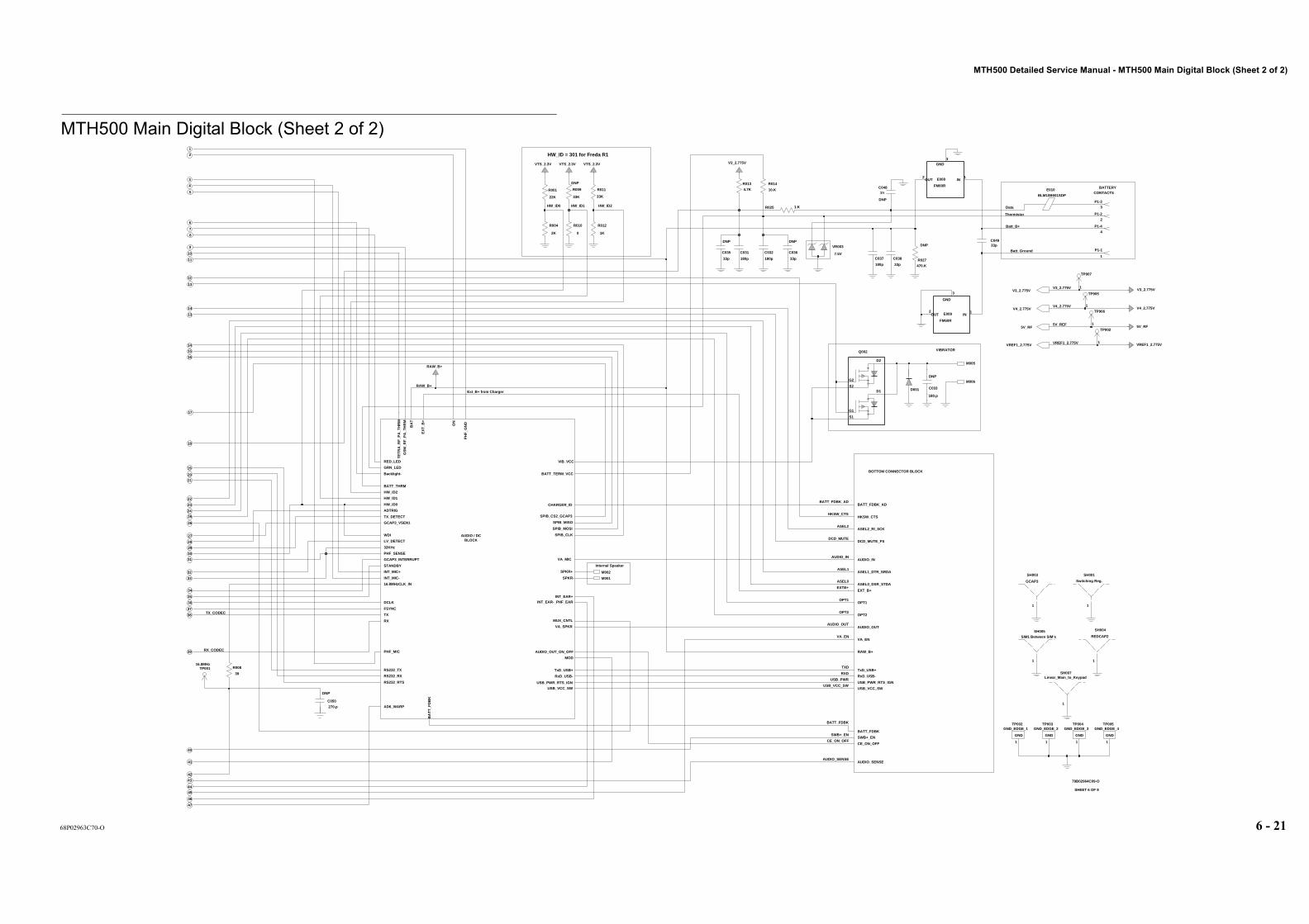
MTH500 Detailed Service Manual - MTH500 Main Digital Block (Sheet 2 of 2)
68P02963C70-O 6 - 21
MTH500 Main Digital Block (Sheet 2 of 2)
Internal Speaker
Data
Batt_Ground
Thermistor
Batt_B+
Ext_B+ from Charger
RX_CODEC
RAW_B+
TX_CODEC
BATTERYCONTACTS
OPT2
RXD
DCD_MUTE
ASEL0
ASEL1
OPT1
ASEL2
AUDIO_OUT
TXD
BATT_FDBK_AD
EXTB+
BATT_FDBK
CE_ON_OFF
SWB+_EN
HKSW_CTS
USB_PWR
AUDIO_IN
AUDIO_SENSE
VIBRATOR
HW_ID = 301 for Freda R1
VREF1_2.775V
5V_REF
V4_2.775V
V3_2.775V
HW_ID2HW_ID1HW_ID0
VA_EN
DNP
USB_VCC_SW
DNP
16.8MHz
DNP
1
2
3
4
5
6
7
8
9
10
11
12
13
14
13
14
15
16
17
18
19
20
21
22
23
24
25
26
27
28
29
30
31
32
33
34
35
36
37
38
39
40
41
42
46
47
44
45
43 79B02964C09-O
SHEET 6 OF 9
DNP
DNP DNP
22K 33K 33K
2K 0 1K
DNP
1
P1-1
4
P1-4
M006
2
P1-2
M001
3P1-3
C050
BLM10B601SDP
E010
270.p
R027
470.K
C04933p
FM60R
E009
GND
3
IN1
OUT2
FM60R
E008
GND3
1INOUT
2
C0481n
G1
G2
S1
S2D001
Q002
D1
D2
1.KR025
SH007Linear_Main_to_Keypad
1
GND_EDGE_3TP004
1
GND
GND_EDGE_4TP005
1
GND
GND_EDGE_1TP002
1
GND
GND_EDGE_2TP003
1
GND
SIM1 Between SIM’sSH005
1
1
REDCAP2
SH004
1
Switching Reg.
SH001
1
GCAP3
SH003
TP001
VTS_2.3V
R012
R001
R004
M002
M005
VTS_2.3V VTS_2.3V
VREF1_2.775V
TP902
1
VR003
7.5VC037
180p
C038
33p
C036
33p
C035
33p
BATT_FDBK
BATT_FDBK_AD
CE_ON_OFF
DCD_MUTE_FS
EXT_B+
HKSW_CTS
OPT1
OPT2
RAW_B+
RxD_USB-
SWB+_EN
TxD_USB+
USB_PWR_RTS_IGN
USB_VCC_SW
VA_EN
R009
ASEL0_DSR_STDA
ASEL1_DTR_SRDA
ASEL2_RI_SCK
AUDIO_IN
AUDIO_OUT
AUDIO_SENSE
TP906
1
1
V4_2.775V
TP905
1
5V_RF
R008
V3_2.775V
TP907
TxD_USB+
USB_PWR_RTS_IGN
USB_VCC_SW
VA_MIC
VA_SPKR
VIB_VCC
WDI
39
RED_LED
RS232_RTS
RS232_RX
RS232_TX
RX
RxD_USB-
SPIB_CLK
SPIB_CS2_GCAP3
SPIB_MISO
SPIB_MOSI
SPKR+
SPKR-
STANDBY
TE
TR
A_R
F_P
A_T
HR
M
TX
TX_DETECT
GRN_LED
GS
M_R
F_P
A_T
HR
M
HW_ID0
HW_ID1
HW_ID2
INT_EAR+INT_EAR-_PHF_EAR
INT_MIC+
INT_MIC-
LV_DETECT
MOD
MUX_CNTL
ON
PH
F_G
ND
PHF_MIC
PHF_SENSE
16.8MHzCLK_IN
32KHz
AD6_WARP
ADTRIG
AUDIO_OUT_ON_OFF
BA
T
BA
TT
_FD
BK
BATT_TERM_VCC
BATT_THRM
Backlight-
CHARGER_ID
DCLK
EX
T_B
+
FSYNC
GCAP3_INTERRUPT
GCAP3_VSEN1
RAW_B+
180.p
R010
4.7K
V3_2.775V
C033
R013
C031
180p 180p
R014
C032
10.KR011
V4_2.775V
5V_RF
VREF1_2.775V
V3_2.775V
AUDIO / DCBLOCK
BOTTOM CONNECTOR BLOCK

SCHEMATIC DIAGRAMS - MTH500 Audio & DC Block (Sheet 1 of 2)
6 - 22 68P02963C70-O
MTH500 Audio & DC Block (Sheet 1 of 2)
STANDBY
BATT_TERM_VCC
HW_ID1
HW_ID2
TETRA_RF_PA_THRM
GSM_RF_PA_THRM
RxD_USB-
TxD_USB+
USB_PWR_RTS_IGN
RS232_RX
USB_VCC_SW
GCAP3_VSEN1
WDI
RS232_RTS
BAT
V4_2.775V
TP605
35
36
37
38
39
40
For P2.0 only
P2.6
TX
EN
B
VM
VP
SLUMP DETECTOR
Dual band
Dual band
DNP
BLM21P300S
DNP
DNP
ON\32kHz
MU
X_C
TL
AD
7
AD
8
RE
F1_
VC
C
RE
F1
RE
F1
L2
U600
GCAP3
C732KHZ
L3A1L_IN
4.7u
C653
ON3
Dual band
USB_PWR 3.3V
1
2
3
4
5
6
7
8
9
10
11
12
3.6 VOLTS
MOBPORTB
TX PEAK
CHARGE
MAIN
PWM Filter
SPI_CLK
SPI_DR
SPI_DW
INTERRUPT
STANDBY
WDI
TX
RX
CLK_IN
DCLK
FSYNC
CE
ON
VSEN1
43
44
13
14
15
16
17
18
19
20
21
42
41
22
23
24
25
26
27
28
29
30
31
32
33
344.7u
C626
2.2KR609
C632 1.u
R614 1.K
R613 1.K
R607 2.2K
R606 2.2K
C601
10u100.n
C642
100.n
C641
4.7UH
2 1
FREQ
32.768K
Y600
21
L600
R615
FILT_B+
75.K
R600
FILT_B+
56.K
R605
NEG POS
0.24CR600
18pF
C638
18pF
C637
C646
FUSED_B+
180.p 100.n
C640
C600
100.n
A6
E600
N2
VIN
2
G12
VIN
3
N12
VS
EN
1
VS
IM1
M13
M12
VS
IN
K13
WD
I
B10XRXD
A7
XT
AL
1
XT
AL
2
V2
H14
V3
K14
V4
J11
V4D
RV
A3
VA
G
M7
VIB
_OU
T
M8
VIB
_VC
C
E13
VIN
1
E9USB_POS
F13USB_PWR
F14USB_VCC
J13
US
B_V
CC
R
E10USB_VM
D10USB_VP
B4
UV
SE
L
E14
V1
P1
TSX1M4
TSX2L4
TSY1
TSY2P3
N5
TS
_BY
P
C5TX
B14
TX
EN
B
C9USB_NEG
K6
TH
ER
MB
IAS
K10
TH
GN
D1
L10
TH
GN
D2
L8
TH
GN
D3
H5
TH
GN
D4
G11
TH
GN
D5
K9
TH
GN
D6
TH
GN
D7
F5
N4
C8SR_IN
E7SR_OUT
D8SR_VIN
A8SR_VOUT
C4STANDBY
H3ST_COMP
G1ST_REF
F10TERM4
N1SPKRN
F1SPKROUT1
F2SPKROUT1L
M2SPKRP
H2SPKR_GND1
L1SPKR_GND2
SPKR_OUT2G3
B8SR_EXT
SIMI_O
SIM_PD1E11
E12SIM_PD2
L12SPI_CLK
L13SPI_DR
SPI_DWL11
K12
SP
I_V
CC
M1SPKRIN
RE
F2
RE
F2_
VC
CB
9
A11
RE
F3
B11
RE
F3_
VC
C
N14RESETB
B6
RT
C_G
N
B5RX
A10SE0_IN
M11
PGM2
N8
PG
ND
M9
PS
RC
1
PS
RC
2K
8
H13
RE
F1A
H12
RE
F1B
J14
RE
F1_
VC
CA
J10
RE
F1_
VC
CB
A9
PA
_ON
1P
13P
A_S
EN
SE
PGA_INLF4
F3PGA_INL2
E4PGA_INR
E1PGA_INR2
J2PGM0
J4PGM1
K1
N6
MO
BP
OR
TB
N3MOD
C12
MU
X_C
TL
D13
NC
J5ON
D6ON2
K4ON3
N13
PA
_DR
VP
14
MA
IN_F
ET
C2MB_CAP1
MB_CAP2D1
J12
MF
ET
_LO
W
A2MICINN
D2MIC_BIAS1
MIC_BIAS2E2
B2MIC_OUT
P10
LS
1_O
UT
P11
M10
LS
2_IN
N10
LS
2_O
UT
LS
3_R
XP
12
N11
LS
3_T
X
P9
LX
1
P8
LX
2
P6
N9
FB
1
L9
FB
2
D5FSYNC
A5INTERRUPT
K7
ISE
NS
E
D14LEDG
G10LEDR
B7
LIC
EL
L
LS
1_IN
DSC_INNB12
DSC_INP
G13
DS
C_P
WR
DS
C_S
PL
YG
14
A13
DW
N_I
NB
13D
WN
_OU
T
K3EXTOUT
EXT_MICC3E5
DCLK
H4
DG
ND
1K
11D
GN
D2
C11
DG
ND
3
DG
ND
4A
4
DINC10
A14DSC_EN
C13DSC_EN_OUT
A12
E8
BL
_SIN
KP
7B
PL
US
B3
CD
_CA
P
L14CE
CH
AR
GE
D7
M6
CH
RG
C
C6CLK_IN
D11CMP_OUT
G2ALRT_REF
J3ALRT_VCC
B1AUX_MICN
C1AUX_MICP
D3AUX_OUT
L7
BA
TT
ER
Y
BA
TT
_FD
BK
N7
P5
BG
_BY
P
L6
AG
ND
5H
11A
GN
D6
AG
ND
7H
10
F11
AG
ND
8D
9A
GN
D9
H1ALRTIN
J1ALRTOUT
K2ALRTOUTP
ADTRIG
E3
AG
ND
1E
6A
GN
D10
G5AGND11A
F12AGND11B
G4
AG
ND
2
AG
ND
3M
3
P2
AG
ND
4
A1L_OUT
D4A1_INT
M5AD4
L5AD5
K5AD6
C14
AD
7
D12
AD
8
P4AD9
M14
PWM1_5.6VVSIM1
VIN5
VOUT
100.n
C650
U601
LP2980
2G
ND
NC43
ON_OFF*
1
VTS_2.3V
VTS_2.3V VTS_2.3V
39.K
R622
39.K
R621
R620
V2_2.775V
39.K
R650
39.K
R651
1.K
V1_2.775V
D601
0.
R647
5V_RF
FILT_B+
R646
56.K
56.K
R645
C615
5V_RF
C614
10u
V3_
2.77
5V
FILT_B+
4.7u
C639
C627
4.7u
100.n
0.047u
C662
1.5K
R643
39.K
R642
TP604
TP603
1K
TP601
R640
V3_2.775V
2.2KR630
100n
C656
3.3K
R618
G2
S1
S2
TP600
D1A
D1B
D2A
D2B
G1
V3_2.775V
Q600
15u
L601
C623
NEG POS
68uF
PWM1_5.6V
MBRM120L
CR602
100.n
C643
R616 10.M
MBRM120LT3
NEGPOS
CR601
F600
7.5
VR601
2.5A
C651
180.p
10.u
C652
C649
V3_2.775V
4.7u
1.uC631
1.uC630
47.0u
L602
C648CR603
MBRM120L
NEG
POS180.p
PWM2_1.8V
C624
33uF
2.2K
R617
AD6_WARP
LV_DETECT
V4_DRV
INT_MIC-
INT_MIC+
PHF_MIC
VA_MIC
ON
VIB_VCC
SPIB_CLK
SPIB_MOSI
SPIB_MISO
GCAP3_INTERRUPT
Backlight-
RX
TX
16.8MHzCLK_IN
DCLK
FSYNC
SPIB_CS2_GCAP3
GRN_LED
RED_LED
EXT_B+
MOD
AUDIO_OUT_ON_OFF
PHF_GND
32KHz
PHF_SENSE
BATT_THRM
CHARGER_ID
HW_ID0
ADTRIG
BATT_FDBK
TX_DETECT
RS232_TX

MTH500 Detailed Service Manual - MTH500 Audio & DC Block (Sheet 2 of 2)
68P02963C70-O 6 - 23
MTH500 Audio & DC Block (Sheet 2 of 2)
42
43
44
SHEET 8 OF 9
79B02964C09-O
8
6
7
9
10
5
14
- Vibrator
13
12
DNP
1
2
3
4
11
C605
VSIM
TP602
C663
R649
3.3n
PGM1 = 0
VIB_VCC
External LP2980 regulator 3.0V for QVCCM
Bias current for the A/D inputsVTS_2.3V
WPIC, ODCT, LVFracN, ...V4_2.775V
V1_2.775V
Dual band
NU
VREF2_2.775V
VSIM1 -
PGM2 = 1
DNP
DNP
DNP
PGM0 = 1
TP connected to Redcap MUX_CNTL pin
Leds and Backlight
- 3.6V nominal - RF PA, TX Pre-drivers, ODCT Up-mixer
- RAW_B+ thru ferrite bead with bypass caps
- 5.0Vdc to WPIC Charge Pump
DC Power Supply Distribution
Digital section - Redcap, Flash, RAM, Display
- Audio
- 5.6Vdc (GCAP3 switching regulator #2 - BOOST) to the input of DSC regulator (5.0Vdc) to the WPIC Charge Pump , VSIM1
- 1.875Vdc(GCAP3 switching regulator #1 - BUCK) to REDCAP core
V2_2.775V
V3_2.775V
5V_RF
RAW_B+
FILT_B+
PWM2_5.6V
PWM1_1.8V
RF TCXOVREF1_2.775V
SW_B+ Battery Voltage for CE bus with the Current limit function
C647
15
16
17
18
19
20
21
22
23
24
25
26
27
28
29
30
31
32
33
34
35
36
37
38
39
40
41
180.p
C619
E604
BLM11B601S
100.n
BLM11B601S
E603
4.7u
C629
R648
C6592.7K
4.7u4.7u
C658
4.7u
C609
C657
V3_2.775V
C613
4.7u
V2_2.775V
4.7u10.u
C610
R623
0.
4.7u
VREF2_2.775V
V4_DRV
C654 1.u
VREF1_2.775V
10.u
V1_2.775V
C628
C611
100.n
C608C616
10.u
C607
FILT_B+
R603
100.n
75K
100.n
C606
1.u
C635
C604
100.n
FILT_B+
C621 1n
C620
R601 33K
180.p
C625
100u 180.p
390.pC664
100
4.7u
C612 C660
4.7u
C661
4.7u
C636 390.p
R632
100
R631 100
10n
C655
R629 6.2K
0.
R627R624
0.0.
R626
0.
R625R628
0.
R608 22KC634 1.u
C618 C617
180.p180.p
E602
BLM11B601S
E601
BLM11B601S
C603
33K
1n
R612
6.2KR611R610 22K
C602
10n
1.uC633
R604 75K
C622 390.p
R602
FILT_B+ V4_2.775V
75K
100.n
C644
Q602
1
2
3
SPKR-
SPKR+
VA_SPKR
MUX_CNTL
INT_EAR-_PHF_EAR
INT_EAR+

SCHEMATIC DIAGRAMS - MTH500 REDCAP 2 Block (Sheet 1 of 2)
6 - 24 68P02963C70-O
MTH500 REDCAP 2 Block (Sheet 1 of 2)
19
2
4 3 2 1
3
5
1
O
SWB+_EN
NU
NU
NU
O
SYNT
O
O
II
ODISPLAY RS
BAT_DATA
O
O
O
O
O
I/O
AUDIO_IN
SWB+ Voltage enable for the CE bus
NU
DIS
PL
AY
_RS
O
I
WPIC Serial Port SRD Pin 77
OTCXO_WARP
O
O
VIBR_EN
I
I
I
IINT0 - PTT
O
O
I
MOD
RESET_OUTRESET_OUT
SIM_CARD
TX_DETECT
Sam
sun
g 5
12k
x16
I
SPIB
WPIC Serial Port STD Pin 83
WPIC Serial Port CLK Pin 25
WPIC Serial Port Frame Sync Pin 24
O
O
O
INT1 - GCAPIII INT
RESET_2.5V-2.7V Low_Voltage_Dector (Connect to GCAP3 RESETB Pin)
INT4 - Option_Select_1
INT5 - Option_Select_2
I
I
I
I
KEYPAD
PT
T
ON
/OF
F f
rom
GC
AP
3
Op
tio
n_S
elec
t_1
Op
tio
n_S
elec
t_2
IGCAP3 Audio Serial Port Frame Sync
Internal Pulldown
INPUTS
RESET_OUT
16.8 MHz InputI
32.768 kHz Input
OE
INTERRUPT
GCAP3
I
O
Connect to GCAP3 WDI Pin
INT0 - PTT
INT1 - GCAPIII INT
INT4 - Option_Select_1
INT5 - Option_Select_2
RTS
RX
TX
ROW7
ROW6
INT6
INT7
SYMBOL
PIN NAME
Gen Port Ctrl Reg (GPCR)GPCR = xxxxxxxx x11xxx11
Gen Port Ctrl Reg (GPCR)GPCR = xxxxxxxx x00xxx00
GPCR (Bit7)=1GPCR (Bit7)=0
I
I
O
O
O
O
O
I
I
I
O
O
O
O
O
I
I
I
I
O
NOTE: RESETS FROM THE BOTTOM CONNECTOR WILL ONLY BE POSSIBLE IF
MUX_CTRL =1 AND THE 8-WIRE INTERFACE IS THUS SET TO JTAG MODE
32.768 kHz Input
16.8 MHz InputI
Un
use
d G
PO
Un
use
d G
PO
Un
use
d G
PO
Un
use
d G
PO
Un
use
d G
PO
Un
use
d G
PO
O
O
O
O
O
LA
YE
R1
TIM
ER
RI
DCD
DSR
DTR
8-Wire RS232
STDA
SRDA
SB9600
ESSI
MUX_CTRL=1MUX_CTRL=0
DSP_DE
CTS
REDCAP2
17x17mm BGA
CS2#-SRAM
FLASH2 Meg x16
WPIC
ODCT
FL
AS
H
SR
AM
RA
DIO
SO
FT
TU
RN
OF
F
NU
RESET_OUT
SPIA
GCAP3 Audio Serial Port Clock
DSP_SRD goes to GCAPIII_TX
DSP_STD goes to GCAPIII_RX
CTS
RTS
RX
TX
WPIC
I
I
O
O
O
O
O
MCU_DE
RESET_IN
TDI
TDO
TCK
TRST
TMS
JTAG
CTS
RTS
RX
TX
SCKA
SC2A
STDA
SRDA
4-Wire RS232
ESSI
BUSY_OUT
BUSY_IN (IC2)
RX
TX
SCKA
SC2A
TP414
100.n
C430
R417
6.8K
TP411
TP412
TP413
TP409TP410
TP407
TP408
C426 10n
C425
10n
14
TP402
1
TP405
VS
S2
E3
VS
S3
8
9
10
11
12
13
G5
LBA1
G2NC1
NC2H6
B2UB
E1
VC
C1
D6
VC
C2
VS
S1
D1
E6
D4F5
D5F6
D6G6
D7B1
D8C1
D9
B6DO
EN_OEA2
EN_WE
D10D2
D11E2
D12F2
D13F1
D14G1
D15
C6D2
D5D3
E5
A5C4
A6D4
A7H2
A8H3
A9
B5CS1
A6CS2
C5D1
C2
A14
A15F4
E4A16
A17D3
H1A18
A5A2
B3A3
B4A4
C3
K6F8016U6AA3A0
A4A1
H4A10
H5A11
G3A12
G4A13
F3
V3_2.775V_FLTR
U402
TP4011
V3_2.775V_FLTR
0R401
21
18
0
V3_2.775V_FLTR
21
TP4031
C412 100.n
100.n
C401
F1
GN
D2
NC1C4
F5
VC
CE
1V
CC
Q
A4
VP
P
5
DQ8D6
DQ9E6
EN_CED7
EN_OEF8
EN_RPB4
EN_WEB3
A5EN_WP
E8
GN
D1
DQ14D2
DQ15E2
DQ2D5
DQ3E5
DQ4F4
D3DQ5
DQ6E3
DQ7F2
A3A8
C3A9
DQ0E7
DQ1F7
DQ10F6
DQ11D4
DQ12E4
DQ13F3
A6A19
B8A2
C5A20
C7A3
A8A4
B7A5
C6A6
A7A7
A2A11
C2A12
A13A1
B1A14
C1A15
D1A16
B6A17
B5A18
28F320C3
U403
D8A0
C8A1
B2A10
4
6
33
2
2 3 4 5
15
6
4
N8
XY
D6
M6
XY
D7
XY
D8
L10
XY
D9
M9
XZ
YR
WC
4
B5
XY
SE
L
XY
ST
B4
1
N9
T9
XY
D13
XY
D14
R9
P9
XY
D15
M5
XY
D2
P8
XY
D3
R8
XY
D4
T8
XY
D5
A1
XY
A7
C2
C3
XY
A8
D1
XY
A9
R7
XY
D0
T7
XY
D1
XY
D10
M10
XY
D11
M11
XY
D12
XY
A12
XY
A13
E1
E3
XY
A14
XY
A15
E4
XY
A2
B3
XY
A3
B2
XY
A4
A3
XY
A5
A2
XY
A6
B7
H14
TR
ST
G15TXA_TDO
TXBK11
XY
A0
A4
XY
A1
D4
D2
XY
A10
D3
XY
A11
E2
E8
D5TOUT2
C6TOUT3
B6TOUT4
A6TOUT5
D6TOUT6
D7TOUT7
TOUT8C7
TOUT9
TM
S
A5TOUT0
C5TOUT1
TOUT10B8
TOUT11A8
TOUT12D8
TOUT13E6
TOUT14E7
TOUT15
B12
D16STDA
A14STDB
T13STO
H13
TC
KG
12T
DI
F12
TD
O
G16
TE
ST
H12
SPICS3A
SPICS3BA10
F7SPICS4A
E12SPICS4B
A9SPI_CKA
SPI_CKBD11
D13SRDA
B14SRDB
SRDB2
SIZ
0F
14S
IZ1
D9SPICS0A
SPICS0BD10
E11SPICS1A
SPICS1BC10
E10SPICS2A
SPICS2BB10
E9
SC2B
C15SCKA
C13SCKB
SCKB2A12
SE
NS
EP
12
N11
SIM
CL
K
N12
SIM
DA
TA
T12
SIM
RE
SE
T
F15
RW
G14RXA_IC1_TDI
RXBJ12
SC0AB16 B13
SC0BA16
SC1AA13
SC1BA15
SC2AC14
ROW2K15
ROW3J14
ROW4
ROW5_IC2BJ15
J16ROW6_DCD_SC2A_DSP_DE
J13ROW7_RI_SCKA_TCK
G13RTSA_IC2A_RESET_IN
RTSBK12
M2
PS
TA
T2
D15
PS
TA
T3
T10PVCC
PW
R_E
NT
11
R13RESET_IN
P13RESET_OUT
L15ROW0
K13ROW1
K14
D12
F16MUX_CTL
M1
OE
P1GNDN10
R10PCAP
P10PGND
E13
PS
TA
T0
PS
TA
T1
E15
D14
INT
5M
13IN
T6_
DS
R_S
TD
A_T
RS
TL
14IN
T7_
DT
R_S
CL
K_S
RD
A_T
MS
MC
U_D
EH
11
B9MISOA
MISOBC11
R12
MO
D
C9MOSIA
MOSIB
DS
P_I
RQ
K1
EB
0J3
EB
1
INT
0N
16
N15
INT
1N
14IN
T2
M15
INT
3M
16IN
T4
M14
R3
P3D4
T4D5
R4D6
P4D7
P5D8
N5D9
G11
DS
P_D
E
C12
T2
P6D10
R6D11
T6D12
N6D13
N7D14
P7D15
T3D2
D3
CS
1P
2C
S2
R2
CS
3P
1C
S4
R1
CS
5
F13CTSA_MCU_DE
CTSBL12
T1D0
D1
COLUMN1R15
COLUMN2T14
COLUMN3R16
COLUMN4P16
COLUMN5P15
COLUMN6_OC1P14
COLUMN7
N3
CS
0N
2
ADDR7H5
ADDR8G5
ADDR9
K4CKIH
CKILK2
M3CKO
L2CKOH
N13COLUMN0
R14
ADDR19
ADDR2J4
F2ADDR20
F3ADDR21
ADDR3L5
K6ADDR4
J6ADDR5
H6ADDR6
G6
ADDR11
ADDR12H1
H2ADDR13
H3ADDR14
ADDR15E5
G3ADDR16
G4ADDR17
F4ADDR18
F1
U401
30C40
J2ADDR0
J1ADDR1
F5ADDR10
H4
12
13
14
15
15
8
9
10
11
11
12
13
14
15
10
11
12
8
9
10
5
6
7
8
9
7
1
2
3
4
1
2
3
4
5
6
16
17
18
19
0
0
1
2
3
4
5
6
7
13
14
15
1
2
8
9
10
11
12
3
4
5
6
7 5
6
7
0
1
2
19
1
2
3
4
14
15
16
17
18
8
9
10
11
12
13
3
4
5
6
7
14
15
16
17
PWM2_1.8V_FLTR
20
20
13
22.KR405
10uF
C415
U405R407
47.
C422
10.n
DISPLAY_RS
VIBR_EN
TCXO_WARP
C423
6.8n
MEM_CNTL(6:1)
SPIB_CS2_GCAP3
SPIB_MISO
SPIB_CLK
SPIB_MOSI
SPIB_CS1_DISPLAY
SIM_BUS(5:1)
VA_EN
WPIC_OSC_EN
GCAP3_STANDBY
AUDIO_SENSE
BAT_DATA
MOD
SOFT_TURN_OFF
SWB+_EN
SIM_DATA
SIM_POWER
SIM_RESET
SIM_CLOCK
CS2_
EB1
EB0
WPIC_SRD
KP_ROW4
TX_DETECT
RX_ACQ
TETRA_MAIN_VCO_ON
SYNT_CS_
RESET_OUT
RESET_OUT
RS232_DTR
RS232_DSR
16.8_MHz_CLK
KP_COL0
KP_COL1
KP_COL2
KP_COL3
KP_COL4
KP_ROW0
KP_ROW1
KP_ROW2
KP_ROW3
LV_DETECT
GCAP3_FSYNC
GCAP3_DCLK WPIC_TXCLK
GCAP3_TX
GCAP3_RX WPIC_STD
LO_Driver_En
LO_Mixer_En
WPIC_TXE
PA_Bias
GCAP3_AD_TRIGGER
ANT_EN
RS232_TX
HST_Addr(0:21)HST_DATA(0:15)
SPIA_CS0_WPIC
SPIA_MISO
SPIA_CS2_ODCT
SPIA_CLK
32KHz_CLK
RS232_CTS
PTT
GCAP3_INT
OPT_SEL_1
OPT_SEL_2
MCU_DE
SPIA_MOSI
MUX_CTRL
RS232_DCD
RS232_RI
RS232_RTS
RS232_RX
WPIC_FSYNC
AUDIO
CODEC
QSPI-A
QSPI-B
EIM
EMU AND DEBUG INTERRUPTS
KEYPAD
UART-B
UART-A
CLOCK AND PLL
LAYER1 TIMER
BASEBANDCODEC PORT
JTAG AND TEST SMART CARD

MTH500 Detailed Service Manual - MTH500 REDCAP 2 Block (Sheet 2 of 2)
68P02963C70-O 6 - 25
MTH500 REDCAP 2 Block (Sheet 2 of 2)Bypass Caps for REDCAP
REDCAP2
PWR, GND, NC
Ad
dre
ss B
us
Bu
s C
on
tro
l
Dat
a B
us
Au
dio
Co
dec
Po
rt
Clo
ck O
utp
ut
Dri
ver
Bo
tto
m, G
PIO
, JT
AG
, DE
BU
G, D
AT
A,S
TO
QS
PI &
L1T
& B
BP
EM
UL
po
rt
SIM
CA
RD
Inte
rnal
Co
re
Co
re V
olt
age
Co
nve
rto
rs
DS
P A
dd
ress
vis
ibilt
y
DS
P D
AT
A v
isib
ilty
VCC TRUTH TABLE
PWM2_1.8V = 1.875V (Redcap Core, ADDR/Data Bus, Flash, SRAM.
V3_2.775V = 2.775V (from GCAP3 V3)
PWM2
V3
VSIM1 = 3V for the SIM port and QVCCH
VSIM1
79B02964C09-O
SHEET 7 OF 9
C429
100n
100n
C428
100n
C427
C424
100n
VSIM1
PWM2_1.8V_FLTR
V3_2.775V_FLTR
10.u
C416
E401
V3_2.775V
PWM2_1.8V
E400
1.u
C420C414
180p
1.u
C421
180p
C413
QV
CC
2L
4
QV
CC
3L
13
QV
CC
4M
7
QV
CC
H1
F9
J11
QV
CC
H2
QV
CC
H3
M8
QV
CC
H4
K3
NC7H8
NC8H9
NC9H10
QG
ND
1F
10
QG
ND
2L
1
QG
ND
3L
7
QG
ND
4L
16
QV
CC
1F
8
K10NC17L6NC18L11NC19
NC2G7
NC3G8
NC4G9
NC5G10
NC6H7
NC1F11
NC10J7
NC11J8
NC12 J9
NC13 J10
K7NC14K8NC15K9NC16
C8
HV
DD
2
KG
ND
E14
KV
DD
E16
C1
LG
ND
B1
LV
DD
MG
ND
L9
MV
DD
L8
NC0F6
GG
ND
2K
16
T15
GG
ND
3
GV
DD
1H
16
GV
DD
2M
12
T16
GV
DD
3
A7
HG
ND
1
HG
ND
2A
11
HV
DD
1B
11
CV
DD
N1
DG
ND
T5
DV
DD
R5
EG
ND
C16
EV
DD
B15
FG
ND
L3
FV
DD
M4
GG
ND
1H
15
AG
ND
1G
2
AG
ND
2K
5
AV
DD
1G
1
AV
DD
2J5
BG
ND
P11
BV
DD
R11
CG
ND
N4
PWR_GND_NC
U401
C418
.01uF
.01uF
C417 C419
.01uF
100.n
C402C405
100.n
C407
100.n
C404
100.n
C409
100.n
C410
10.n
C406
100.n 100.n
C408C403
10.n
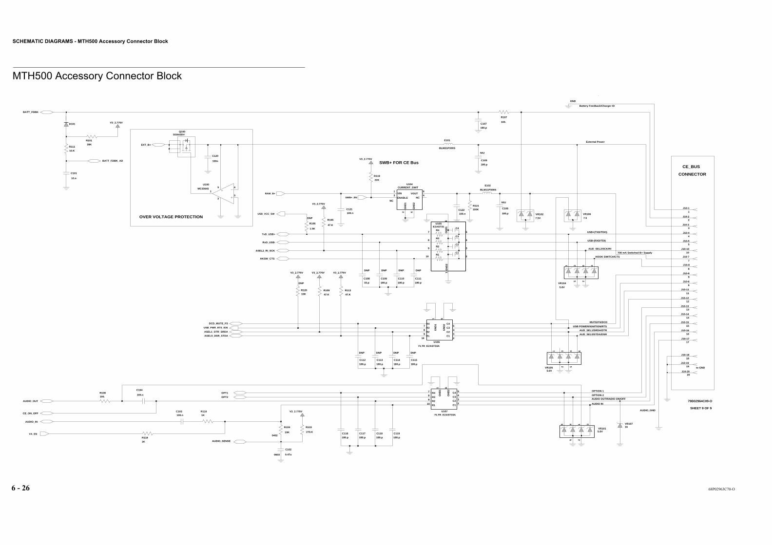
SCHEMATIC DIAGRAMS - MTH500 Accessory Connector Block
6 - 26 68P02963C70-O
MTH500 Accessory Connector Block
DNP
Battery Feedback/Charger ID
External Power
USB-(RXD/TDI)
USB+(TXD/TDO)
USB POWER/IGNITION/RTS
700 mA Switched B+ Supply
HOOK SWITCH/CTS
MUTE/FS/DCD
AUD_SEL2/SCK/RI
AUD_SEL1/SRDA/DTR
AUD_SEL0/STDA/DSR
OPTION 1
OPTION 2
AUDIO OUT/RADIO ON/OFF
AUDIO IN
NC
SWB+ FOR CE BusCE_BUS
CONNECTOR
AUDIO_GND
GND
OVER VOLTAGE PROTECTION
BLM21P300S
BLM11P300S
to GND
0603
0402
79B02964C09-O
SHEET 9 OF 9
DNP DNP DNP DNP
DNP DNP DNP DNP
DNP
N/U
N/U
180.p
J10-2020
C105
E101
R108
100.
J10-1818
J10-1919
V3_2.775V
100K
R121
C122
100.n
C121
100.n
10K
R120
V3_2.775V
16VR107
7.5
VR106
E102
9R2
8R3
7R4
2
C1
3
C2
4
C3
5
C4
6G
ND
11
GN
D2
10R1
10R1
9R2
8R3
7R4
EZAST31U105
2C1
3C2
4C3
5C4
1G
ND
1
6G
ND
2
9R2
8R3
7R4
FLTR_EZAST33A
U106
2C1
3C2
4C3
5C4
1G
ND
1
6G
ND
2
10 R1
FLTR_EZAST33AU107
R119
22K
R118
1K
MC33645
U100
32
4
1
5
C120
100n
Q100
V3_2.775V V3_2.775V
SI3443DV
47.K
R113
47.K
R109
16
J10-1717
J10-1515
J10-16
13
J10-1414
J10-1212
J10-13
10
J10-11
11
J10-99
J10-10
J10-7
7
J10-8
8
J10-66
J10-44
J10-55
J10-33
J10-1
1
J10-22
180.p
C119
180.p
C116
180.p
C117
180.p
C118
C115C114
180.p180.p180.p
C113
180.p
C112
33.p
C108
180.p
C111
180.p
C110
180.p
C109
2G
ND
1
5G
ND
2
4NC
1VIN
6VOUT
U104CURRENT_SWIT
3ENABLE
R101
V3_2.775V
R111
10.K
39K
10.n
C101
V3_2.775V
D101
V3_2.775V
R105
47.K1.5K
100.n
C104
R106
100.n
C103
C102
0.47u
R104
10K
R103
270.K
R110
1K
C107
180.p
C106
180.p VR102
5.6V
2 5
1 3 4 6
7.5V
4631
VR105
5.6V
VR104
25
25
3146
100.
R107
5.6VVR101
AUDIO_SENSE
USB_VCC_SW
ASEL2_RI_SCK
BATT_FDBK_AD
SWB+_EN
RAW_B+
USB_PWR_RTS_IGN
EXT_B+
VA_EN
BATT_FDBK
TxD_USB+
RxD_USB-
HKSW_CTS
DCD_MUTE_FS
ASEL1_DTR_SRDA
ASEL0_DSR_STDA
OPT1
OPT2
AUDIO_OUT
AUDIO_IN
CE_ON_OFF

MTH500 Detailed Service Manual - MTH500 (FLF9011A) Component Parts (for reference only)
68P02963C70-O 6 - 27
MTH500 (FLF9011A) Component Parts (for reference only)When ordering component parts, the part number should be included. If the correct numbers cannot be located, call Motorola Parts Identification.
CAPACITORS
Ref # Part # Description Ref # Part # Description Ref # Part # Description Ref # Part # Description Ref # Part # Description
C001 2113743p01 180pF C401-402 2113743M24 100nF C526-527 2113743n26 10pF C608 2113743M24 100nF C701-703 2360567A06 100µF
C002 2113740F39 33pF C403 2113743L41 10nF C528 2113743n24 8.2pF C609 2113928C04 4.7µF C704 2311049G32 10µF
C003 2113740F39 33pF C404-409 2113743M24 100nF C530 2113743L41 10nF C610-611 2113928k09 10µF C800 2113740F49 82pF
C004 2113743p01 180pF C410 2113743L41 10nF C531 2113741F41 4.7nF C612-614 2113928C04 4.7µF C802 2113743L03 270pF
C005 2113743p01 180pF C412 2113743M24 100nF C532 2113743n22 6.8pF C615 2113928D08 10µF C805 2113743L03 270pF
C006 2113743p01 180pF C413-414 2113740F57 180pF C533 2113928U08 10nF C616 2311049A72 Tant. 10µF C808 2113740F57 180pF
C007 2113743p01 180pF C415-416 2311049A59 Tant. 10µF C534 2113743L41 10nF C617-620 2113743p01 180pF C809 2113743L03 270pF
C008 2113743p01 180pF C417-419 2113743L41 10nF C535 2113928n01 100nF C621 2113743L17 1nF C811-812 2113743L03 270pF
C009 2113743p01 180pF C420-421 2113928P04 1µF C536 2113743n34 22pF C622 2113743L07 390pF C814-816 2113743L03 270pF
C010 2113743p01 180pF C422 2113741F49 10nF C539 2113743Q08 1.8pF C623 2311049C16 Tant. 68µF C817 2113740F57 180pF
C011 2113743p01 180pF C423 2113741F45 6.8nF C542 2113743L29 3.3nF C624 2311049C15 Tant. 33µF C819-821 2113743L03 270pF
C012 2113743p01 180pF C424 2113743M24 100nF C545 2113743n19 5.1pF C625 2311049C14 Tant 100µF C822-823 2113741F25 1nF
C013 2113743p01 180pF C425-426 2113743L41 10nF C546 2113743Q07 1.5pF C626-627 2113928C04 4.7µF C824 2113743L03 270pF
C014 2113743p01 180pF C427-429 2113743M24 100nF C547 2113928n01 100nF C628 2113928P04 1µF C827-830 2113743L03 270pF
C015 2113743p01 180pF C430 2113928n01 100nF C549 2113928n01 100nF C629 2113928C04 4.7µF C831 2113743N69 1.8pF
C016 2113743p01 180pF C500 2113743L03 270pF C550-552 2113743l17 1nF C630-635 2113928P04 1µF C832 2113743N46 68pF
C017 2113743p01 180pF C501-502 2113928n01 100nF C553 2113928N01 100nF C636 2113743L07 390pF C833 2113743L09 470pF
C031 2113743p01 180pF C503 2113743L41 10nF C554 2113743E12 47nF C637-638 2113743N32 18pF C834 2113743L03 270pF
C032 2113743p01 180pF C504 2113928n01 100nF C555 2113928n01 100nF C639-643 2113743M24 100nF C835 2113743N32 18pF
C037 2113743p01 180pF C505 2113743L17 1nF C557 2113743E03 15nF C644 2113928n01 100nF C837 2113740F39 33pF
C038 2113743N38 33pF C507 2113743L17 1nF C560-561 2311049A59 Tant. 10µF C646-648 2113740F57 180pF C838 2113743N18 4.7pF
C049 2113743N38 33pF C508 2113928n01 100nF C572-573 2113928n01 100nF C649 2113928C04 4.7µF C839 2113740F47 68pF
C101 2113743L41 10nF C510 2113743L03 270pF C574 2113743L03 270pF C650 2113743M24 100nF C840 2113740F30 18pF
C102 2113928A02 0.47µF C512 2113743L03 270pF C576 2113743L03 270pF C651 2113740F57 180pF C841 2113740F47 68pF
C103-104 2113928n01 100nF C513 2113743L17 1nF C577 2113743L41 10nF C652 2311049G32 Tant. 10µF C842 2113743N34 22pF
C107 2113743p01 180pF C514 2113743L03 270pF C580 2113743l17 1nF C653 2311049C18 4.7µF C843 2113743N30 15pF
C116-119 2113743p01 180pF C515-516 2113928n01 100nF C590 2113743L03 270pF C654 2113928C04 4.7µF C844-845 2113743N28 12pF
C120-121 2113743M24 100nF C518-519 2113928n01 100nF C600 2113743M24 100nF C655 2113743L41 10nF C846 2113743N26 10pF
C122 2113928s04 100nF C521 2113743n15 3.6pF C601 2113928D08 10µF C657-661 2113928C04 4.7µF C847 2113743N24 8.2pF
C200 2113743L03 270pF C522 2113743N50 100pF C602 2113743L41 10nF C662 2113928S02 0.047µF C848 2113743N25 9.1pF
C203 2113743L03 270pF C524 2113743Q08 1.8pF C603 2113743l17 1nF C663 2113743L29 3.3nF
C205 2113743L03 270pF C525 2113743n28 12pF C604-607 2113928n01 100nF C664 2113743L07 390pF

SCHEMATIC DIAGRAMS - MTH500 (FLF9011A) Component Parts (for reference only)
6 - 28 68P02963C70-O
C849 2113743N11 2.4pF C909-910 2113743N50 100pF C984 2113743L37 470pF E007 2409134j04 blm11b601s
C850 2113743N17 4.3pF C915 2113743N50 100pF C1004 2113928n01 100nF E008 9108445S04 fm60r
C851 2113743N13 3pF C916 2113743L17 1nF C1009 2113743L37 6.8pF E009 9108445S04 fm60r
C852 2113740F21 1pF C919 2113743n30 15pF C1010 2113743N22 8.2pF E010 7686949J02 blm10b601sdp
C853-857 2113743L17 1nF C920 2113740F25 8.2pF C1011 2113740F17 3.9pF E101 2480675U01 idctr
C859 2113743L07 390pF C921-922 2113740F27 10pF C1012 2113740L05 3pF E102 7686949J08 idctr
C860 0804533C48 22nF C927 2113740F31 15pF C1014 2113743L03 270pF E201 2480675U01 idctr
C861-862 2113743E05 18nF C929 2113740F20 5.1pF C1015 2113743N20 5.6pF E203 2480675U01 idctr
C863-864 2113741F45 6.8nF C930 2113743N50 100pF C1016 2113743N40 39pF E400-401 2480067M02 blm21a121s
C865 2113743L17 1nF C931 2113740F20 5.1pF C1020 2113928n01 100nF E500-501 7686949J02 blm10b601sdp
C866 2113743L03 270pF C932 2113740F31 15pF C1021 2113743L03 270pF E600 2480675U01 idctr
C867 2113740F35 2.7nF C933 2113743n20 5.6pF C1022 2113928P04 1µF E601-604 2409134J04 blm11b601s
C869 2113928N01 100nF C937 2104263L01 100nF C1023-24 2113743K15 100nF E800 7686949J02 blm10b601sdp
C873 2113743L17 1nF C938 2113743n17 4.3pF C1028 2186113u01 56pF E801 9108445S04 fm60r
C874-875 2113928n01 100nF C939 2113743N15 3.6pF C1029 2113740F30 13pF DIODES E803 2409134J04 blm11b601s
C877-878 2113743cL37 6800pF C940 2113740L01 2pF C1030 2113740F24 7.5pF Ref # Part # Description E806 2409134J04 blm11b601s
C879 2113741F49 10nF C942 2113740F25 8.2pF C1031-1032 2113743L03 270pF CR600-603 4813833a19 mbrm120L E807 7686949j02 blm10b601sdp
C880 2113741f45 6.8nf C946 2113743N50 100pF C1045 2113743L07 390pF D001 4808032h08 1ss355 E808-809 2409134j04 blm11b601s
C881-882 2113741F41 4.7nF C948 2113743L37 6.8nF C1046 2113928W09 47µF D101 4809948D42 1ss367 E810 7686949j02 blm10b601sdp
C883 2113928n01 100nF C951 2113743n28 12pF C1048 2113743L03 270pF D500 4808115L17 tekelec E901 7686949j02 blm10b601sdp
C886 2113740F41 38pF C953 2113743L17 1nF C1050 2113743L03 270pF D601 4809948D42 1ss367 FUSES
C887 2113743N46 68pF C954 2113743L03 270pF D800 4804135k05 1sv231 Ref # Part # Description
C888 2113743L03 270pF C955 2113743L48 22000pF D801 4885908A02 ma4p789 F600 6586221j04 2.5A 16V
C890 2113743N40 39pF C957 2113743L33 4.7nF D902 4809877c13 1sv305
C891 2113743L03 270pF C958 2104263L01 100nF D907 4805656W28 BBY5802W
C894 2113740F51 100pF C959 2113743L17 1nF BEADSC895 2113743L29 3.3nF C960 2113740F24 7.5pF Ref # Part # Description
C897 2113743N38 33pF C961 2113743L48 22nF E001 2409134j04 blm11b601s
C898-899 2113743L03 270pF C962 2113743N33 20pF E002 7686949j02 blm10b601sdp
C901-902 2113928n01 100nF C966 2113743L17 1nF E003 7686949j02 blm10b601sdp
C903 0804533C50 33nF C967 2113743L03 270pF E004 7686949j02 blm10b601sdp
C904 2113743L03 270pF C968 2113743L17 1nF E005 7686949j02 blm10b601sdp
C905-906 2113743N50 100pF C970-971 2113743L17 1nF E006 7686949j02 blm10b601sdp
CAPACITORS
Ref # Part # Description Ref # Part # Description Ref # Part # Description Ref # Part # Description Ref # Part # Description

MTH500 Detailed Service Manual - MTH500 (FLF9011A) Component Parts (for reference only)
68P02963C70-O 6 - 29
FILTERS TRANSISTORS
Ref # Part # Description Ref # Part # Description Ref # Part # Description Ref # Part # Description Ref # Part # Description
FL500 9180310L24 390mhz L530 2409154M21 47n L916 2413926g16 56n Q002 4809579E50 si1905dl R011 0662057N11 33K
FL501 9186216J06 380mhz L600 2408603y01 4.7uh L917 2413926g05 6.8n Q100 4809579E29 si3443 R012 0662057M24 1000K
FL502 9185898A02 109.65mhz L601 2486085A02 15u L918-919 7686949j02 blm10b601sdp Q500 4805723X03 umd3n R013 0662057M90 res_4.7K
FL800 9180310L23 390mhz L602 2486085A05 47uh L920 2460591C23 13.85n Q504 4805723X03 umd3n R014 0662057M98 res_10K
FL801 5804901K15 380mhz L800 2409154M23 68n L921 2486616u01 5.6n Q600 4885140c01 fds6875 R015 0662057m34 res_22
L801 2409377M10 33n L922 7686949j02 blm10b601sdp Q602 4805128M27 bsr33 R016 0662057m34 res_22
CONNECTORS L803 2413926g19 100n L923 2485930822 2.8n Q800 4805723X03 umd3n R025 0662057M74 res_1K
Ref # Part # Description L805 2413926g19 100n L926 2409154M17 22n Q801 4805793y01 ne68519 R101 0662057V17 res_39K
J10 0987636k05 conn_ce L806 2413926g17 68n L930 2486170u01 390n Q804 4805723X03 umd3n R103 0662057n33 res_270K
J700 0987984k02 conn_va L807 2409154M20 39n L931 2486185u01 1u Q805 4805921t11 21t11 R104 0662057M98 res_10K
L808 2409154M17 22n L932 2409154M20 39n Q806-807 4805723X03 umd3n R105 0662057n15 res_47K
L809-810 2409154M14 12n Q808 4809579E41 ne38018 R107-108 0662057m50 res_100
L811-812 2413926m12 8.2n CONTACTS Q900 4805723X02 umt1 R109 0662057n15 res_47K
L813 2413926g11 22n Ref # Part # Description Q903-905 4805793y01 ne68519 R110 0662057M74 res_1K
INDUCTORS L815 2409154M22 56n M001 3986389t01 contact_Spkr Q907 4805723X03 umd3n R111 0662057M98 res_10K
Ref # Part # Description L816 2409154M23 68n M002 3986389t01 contact_Spkr Q910 4805723X03 umd3n R113 0662057n15 res_47K
L500 2487685L08 22n L817 2409377M06 15n M005 3986535t01 contact_Vibrator
L501 2462587V42 470n L818 2487685L08 22n M006 3986535t01 contact_Vibrator
L504 2462587V42 470n L819 2409377M19 128n M500 3986916t01 contact_Ant_Hot RESISTORS
L505 2413926G17 68n L890 2460591C23 13.85n M501 3986917t01 contact_Ant_Gnd Ref # Part # Description
L508 2413926G16 56n L903 2486170u01 390n P1 0989368K01 Connector J R001 0662057n07 res_22K
L512-513 2413926G08 12n L905 2409377M12 47n P15 2886925J04 Connector P R003 0662057n01 res_12K
L518 2409154M19 33n L906 2409154M19 33n R004 0662057M81 res_2k
L519-520 2462587V38 220n L907 2409154M13 10n R008 0662057M40 res_39
L525 2409154M17 22n L912-913 2486170u01 390n R010 0662057M01 res_0
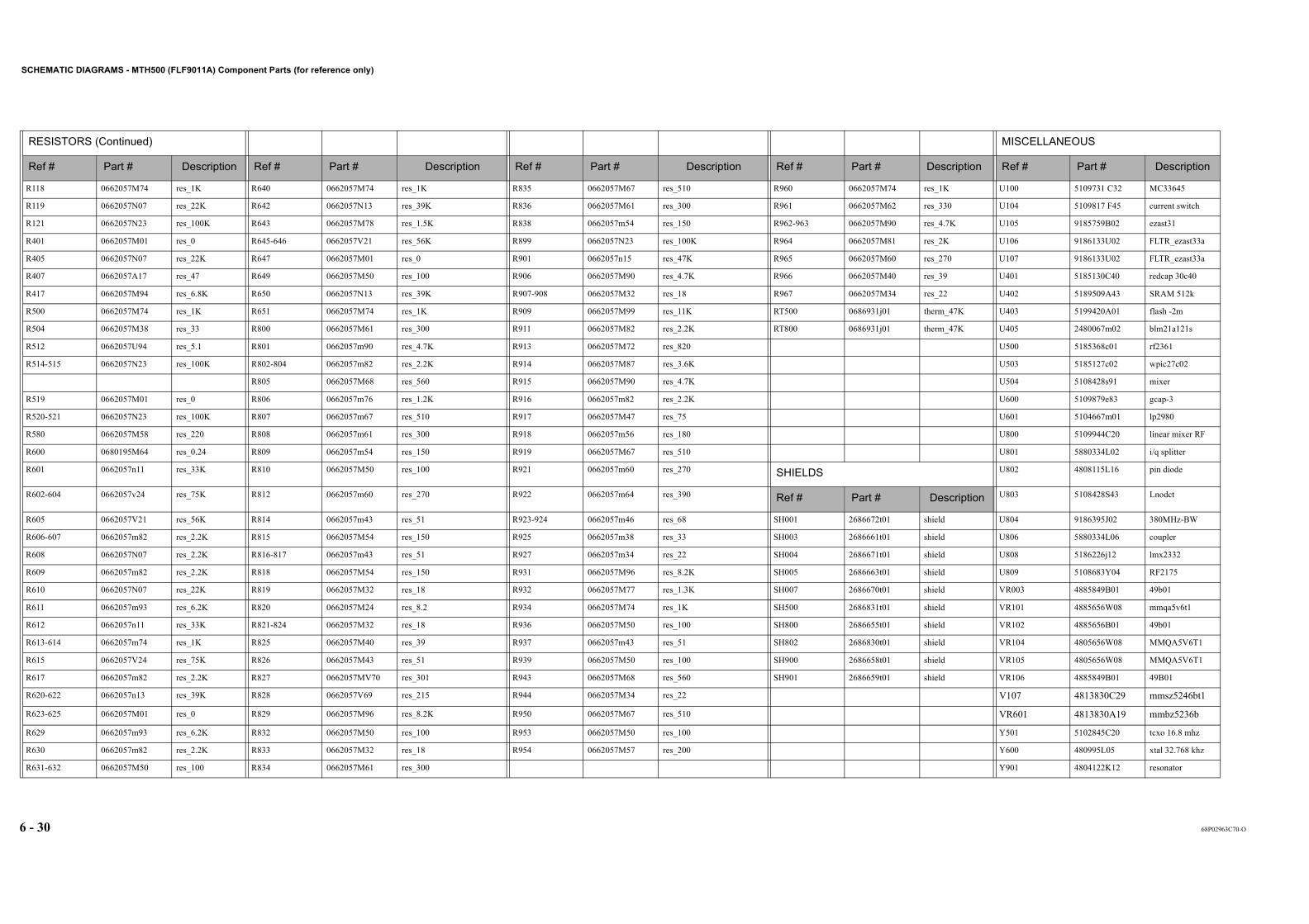
SCHEMATIC DIAGRAMS - MTH500 (FLF9011A) Component Parts (for reference only)
6 - 30 68P02963C70-O
RESISTORS (Continued) MISCELLANEOUS
Ref # Part # Description Ref # Part # Description Ref # Part # Description Ref # Part # Description Ref # Part # Description
R118 0662057M74 res_1K R640 0662057M74 res_1K R835 0662057M67 res_510 R960 0662057M74 res_1K U100 5109731 C32 MC33645
R119 0662057N07 res_22K R642 0662057N13 res_39K R836 0662057M61 res_300 R961 0662057M62 res_330 U104 5109817 F45 current switch
R121 0662057N23 res_100K R643 0662057M78 res_1.5K R838 0662057m54 res_150 R962-963 0662057M90 res_4.7K U105 9185759B02 ezast31
R401 0662057M01 res_0 R645-646 0662057V21 res_56K R899 0662057N23 res_100K R964 0662057M81 res_2K U106 9186133U02 FLTR_ezast33a
R405 0662057N07 res_22K R647 0662057M01 res_0 R901 0662057n15 res_47K R965 0662057M60 res_270 U107 9186133U02 FLTR_ezast33a
R407 0662057A17 res_47 R649 0662057M50 res_100 R906 0662057M90 res_4.7K R966 0662057M40 res_39 U401 5185130C40 redcap 30c40
R417 0662057M94 res_6.8K R650 0662057N13 res_39K R907-908 0662057M32 res_18 R967 0662057M34 res_22 U402 5189509A43 SRAM 512k
R500 0662057M74 res_1K R651 0662057M74 res_1K R909 0662057M99 res_11K RT500 0686931j01 therm_47K U403 5199420A01 flash -2m
R504 0662057M38 res_33 R800 0662057M61 res_300 R911 0662057M82 res_2.2K RT800 0686931j01 therm_47K U405 2480067m02 blm21a121s
R512 0662057U94 res_5.1 R801 0662057m90 res_4.7K R913 0662057M72 res_820 U500 5185368c01 rf2361
R514-515 0662057N23 res_100K R802-804 0662057m82 res_2.2K R914 0662057M87 res_3.6K U503 5185127c02 wpic27c02
R805 0662057M68 res_560 R915 0662057M90 res_4.7K U504 5108428s91 mixer
R519 0662057M01 res_0 R806 0662057m76 res_1.2K R916 0662057m82 res_2.2K U600 5109879e83 gcap-3
R520-521 0662057N23 res_100K R807 0662057m67 res_510 R917 0662057M47 res_75 U601 5104667m01 lp2980
R580 0662057M58 res_220 R808 0662057m61 res_300 R918 0662057m56 res_180 U800 5109944C20 linear mixer RF
R600 0680195M64 res_0.24 R809 0662057m54 res_150 R919 0662057M67 res_510 U801 5880334L02 i/q splitter
R601 0662057n11 res_33K R810 0662057M50 res_100 R921 0662057m60 res_270 SHIELDS U802 4808115L16 pin diode
R602-604 0662057v24 res_75K R812 0662057m60 res_270 R922 0662057m64 res_390 Ref # Part # Description U803 5108428S43 Lnodct
R605 0662057V21 res_56K R814 0662057m43 res_51 R923-924 0662057m46 res_68 SH001 2686672t01 shield U804 9186395J02 380MHz-BW
R606-607 0662057m82 res_2.2K R815 0662057M54 res_150 R925 0662057m38 res_33 SH003 2686661t01 shield U806 5880334L06 coupler
R608 0662057N07 res_2.2K R816-817 0662057m43 res_51 R927 0662057m34 res_22 SH004 2686671t01 shield U808 5186226j12 lmx2332
R609 0662057m82 res_2.2K R818 0662057M54 res_150 R931 0662057M96 res_8.2K SH005 2686663t01 shield U809 5108683Y04 RF2175
R610 0662057N07 res_22K R819 0662057M32 res_18 R932 0662057M77 res_1.3K SH007 2686670t01 shield VR003 4885849B01 49b01
R611 0662057m93 res_6.2K R820 0662057M24 res_8.2 R934 0662057M74 res_1K SH500 2686831t01 shield VR101 4885656W08 mmqa5v6t1
R612 0662057n11 res_33K R821-824 0662057M32 res_18 R936 0662057M50 res_100 SH800 2686655t01 shield VR102 4885656B01 49b01
R613-614 0662057m74 res_1K R825 0662057M40 res_39 R937 0662057m43 res_51 SH802 2686830t01 shield VR104 4805656W08 MMQA5V6T1
R615 0662057V24 res_75K R826 0662057M43 res_51 R939 0662057M50 res_100 SH900 2686658t01 shield VR105 4805656W08 MMQA5V6T1
R617 0662057m82 res_2.2K R827 0662057MV70 res_301 R943 0662057M68 res_560 SH901 2686659t01 shield VR106 4885849B01 49B01
R620-622 0662057n13 res_39K R828 0662057V69 res_215 R944 0662057M34 res_22 V107 4813830C29 mmsz5246bt1
R623-625 0662057M01 res_0 R829 0662057M96 res_8.2K R950 0662057M67 res_510 VR601 4813830A19 mmbz5236b
R629 0662057m93 res_6.2K R832 0662057M50 res_100 R953 0662057M50 res_100 Y501 5102845C20 tcxo 16.8 mhz
R630 0662057m82 res_2.2K R833 0662057M32 res_18 R954 0662057M57 res_200 Y600 480995L05 xtal 32.768 khz
R631-632 0662057M50 res_100 R834 0662057M61 res_300 Y901 4804122K12 resonator

MTH500 Detailed Service Manual - MTH500 Flex CD
68P02963C70-O 6 - 31
MTH500 Flex CD
73B02964C06-O
J2-1
J1-14
J1-15
to keypad to LCD
J1-12
J1-13
J1-10
J1-11
J1-8
J1-9
J1-5
J1-6
J1-7
J1-3
J1-4
J1-1
J1-2
J2-3
J2-2
J2-6
J2-5
J2-4
J2-8
J2-7
J2-10
J2-9
J2-12
J2-11
J2-14
J2-13
J2-16
J2-15
J2-18
J2-17
J2-21
J2-20
J2-19
J1-22
J2-22
J1-20
J1-21
J1-18
J1-19
J1-16
J1-17

SCHEMATIC DIAGRAMS - MTH500 Flex CD
6 - 32 68P02963C70-O
This page left blank intentionally

68P02963C70-O A1 - 1
Appendix 1 ReplacementParts and Kits
REPLACEMENT PARTS AND KITS
Damaged parts should be replaced with identical replacement parts.
Replacement Parts
For complete information on ordering required parts and kits, contact your local customer service representative.
Level 3 Maintenance
EMEA Region
EMEA Radio Support Depots are level 3 service partners. The depots are capable of performing repairs down to component level where retuning is required. Con-tact your local CGISS office for information.
Motorola European Radio Support Centre ERSC Phone: +49 6128 702618Heinrich Hertz Strasse 1D-65232 TaunussteinGermany
ERSC Customer Information Desk available through the following service number:Austria: 06 60 75 41 Italy: 16 78 77 387Belgium: 08 00 72 471 Luxemburg: 08 00 23 27 Denmark: 80 01 55 72 Netherlands: 60 22 45 13Finland: 08 00 11 49 10 Norway: 80 01 11 15France: 05 90 30 90 Portugal 05 05 49 35Germany: 01 30 18 75 24 Spain: 90 09 84 902Greece: 00 80 04 91 29 020 Sweden: 02 07 94 307UK: 08 00 96 90 95 Switzerland: 1 55 30 82Ireland 18 00 55 50 21 Iceland: 80 08 147or dial +49 6128 70 2618Please use these numbers for repair enquires only.

Replacement Parts and Kits
A1 - 2 68P02963C70-O
Latin America Region
Latin America Radio Support CentersThe Customer Support is available through the following service centers:
Warranty and Repairs:Motorola De Colombia Service CenterCarrera 7 No. 71-52Torre B piso 13Oficina 1301Bogota- Colombia(571) 376-6990
Motorola De Mexico Service CenterBosques de Alisos #125Col. Bosques de las LomasCP 05120 Mexico DF5252576700
Piece Parts:To order parts in Latin America and the Carribean:7:00 A.M. to 7:00 P.M. (Central Standard Time)Monday through Friday (Chicago, USA)
1-847-538-8023
Technical Support:https://businessonline.motorola.com, go to Contact Us to request technical sup-port
Motorola Parts (Accessories and Aftermarket Division AAD):Attention: Order Processing1313 E. Algonquin RoadSchaumburg. IL. 60196
Parts Identification:1-847-538-0021 (Voice)1-847-538-8194 (Fax)
Some replacement parts, spare parts, and/or product information can be ordered directly. If a complete Motorola part number is assigned to the part, it is available from Motorola Radio After market and Accessory Division (AAD). If no part number is assigned, the part is not normally available from Motorola. If the part number is appended with an asterisk, the part is serviceable by Motorola Depot only. If a parts list is not included, this generally means that no user-serviceable parts are available for that kit or assembly.

Replacement Parts and Kits
68P02963C70-O 3
Radio Replacement Parts List
Part/Kit Number MTH500 Model Description
0186163T070186163T08
Front Housing Assembly (Black)Front Housing Assembly (Blue)
0186630T01 Keypad Assembly
0186396T040186396T05
Back Housing Assembly (Black)Back Housing Assembly (Blue)
8586381J03 Antenna 380-400 MHz (R1)
0186613T010186613T02
0186239T010186239T02
Standard Battery Door Assembly (Black)Standard Battery Door Assembly (Blue)
Extended Battery Door Assembly (Black)Extended Battery Door Assembly (Blue)
7287702M01 LCD Module
FCN9090A Keypad Kit
FCN9797A LCD Kit
(See Service Replacement Kit Matrix below)
Main Board (R1)

Replacement Parts and Kits
4 68P02963C70-O
Accessories Replacement Parts List
Kit Number MTH500 Model Description
Batteries
FTN6030A Extended battery, 1100mAh, LiIon, Black (with battery door)
FTN6037A Extended battery, 1100mAh, LiIon, Blue (with battery door)
FTN6031A Standard battery, 800mAh, LiIon, Black (with battery door)
FTN6038A Standard battery, 800mAh, LiIon, Blue (with battery door)
Chargers
FLN9468A Dual Pocket Desktop Charger
SPN4716B Travel charger
SYN7455A Plug Adapter UK for travel Charger
SYN7456A Plug Adapter EU for travel Charger
FLN9469A Vehicular battery charger
Vehicular Adapters
FLN2850A Car Kit
FLN9569A Stand alone car cradle
Audio accessories
WADN4184A Headset with Boom mic and in line PTT
FLN9470A Headset with Boom mic (On Hold)
FLN9568A PHF
Carrying Accessories
FLN9476A Soft leather carry case
FHN6246A Belt clip
Others
FKN4897A Data cable
Replacement Parts and Kits
68P02963C70-O 5
Recommended Programming Equipment
Service Replacement Kit Matrix (1)
Note: All models listed in the Service Tanapa Column are not field replaceable for Latin America
Name Part NumberMTH500 CPS PMVN4065BData Cable FKN4897A
Sales Model Description
Service Tanapa
Description
MTH500 Black 380-400 MHzPT811F
FUF1208AS MTH500 BlackS/T R1 CLEAR
FUF1210AS MTH500 BlackS/T R1 TEA1
FUF1211AS MTH500 BlackS/T R1 TEA2
MTH500 Blue380-400 MHzPT811F
FUF1209AS MTH500 BlueS/T R1 CLEAR
FUF1212AS MTH500 BlueS/T R1 TEA1
FUF1213AS MTH500 BlueS/T R1 TEA2

Replacement Parts and Kits
6 68P02963C70-O

Replacement Parts and Kits
68P02963C70-O 7

Replacement Parts and Kits
8 68P02963C70-O

68P02963C70-O A2 - 1
Appendix 2 Test Equipment,Service Aids &
Tools
The table below lists the special test equipment required for servicing MTH500radios.
Name Part Number
Anritsu Digital Signal Generator MG3660A
Power Meter HP437B
Power Supply HP6032A
Universal Multimeter HP3457A
RF Probe HP85024A
Spectrum Analyzer HP8560E
R&S Audio Analyzer UPL16
Data Cable FKN4897
Flash/Data programming cable FLN9636
IFR System 2968

Test Equipment, Service Aids & Tools
A2 - 2 68P02963C70-O
THIS PAGE INTENTIONALLY LEFT BLANK

68P02963C70-O A3 - 1
Appendix 3 Self CheckError/Fail Code Tables
GeneralThis appendix describes the possible self check error codes for the MTH500Portable Radios.
Self Check Error Codes
Table 1. is the possible self check error (non fatal) codes for the MTH500 PortableRadios. No corrective action is required.
Table 2. is the possible self check fail (fatal) codes for the MTH500 Portable Ra-dios. The radio is inoperatable, the user should return the radio to Depot.
Table 2. Self Check Fail (Fatal) Codes
Table 1. Self Check Error (Non-Fatal) Codes
Message Cause
Error00001 A non-fatal error was logged during operation
Error00002 Codeplug error log validity error
Message Cause
Fail00100 Old CodePlug Version failure
Fail00200 New CodePlug Version failure
Fail00400 CodePlug Model failure
Fail00800 Codeplug validity error
Fail00801 CP - Unknown block
Fail00802 CP - Unknown eld
Fail00803 CP - Unknown ag

Connector Pin Functions
A3 - 2 68P02963C70-O
Fail00804 CP - Unknown format
Fail00805 CP - Invalid pointer
Fail00806 CP - Invalid path
Fail00807 CP - Invalid handler
Fail00808 CP - Invalid leght
Fail00809 CP - Invalid index
Fail0080A CP - Invalid offset
Fail0080B CP - Invalid header pointer
Fail0080C CP - Invalid block header
Fail0080D CP - Initialization failed
Fail0080E CP - Recovery failed
Fail0080F CP - Write failure
Fail00810 CP - Corrupted block
Fail00811 CP - Corrupted codeplug
Fail00812 CP - Radio Operattion System eror
Fail00813 CP - Lower layer error
Fail00814 CP - Too many arguments
Fail00815 CP - Log over ow
Fail00816 CP - Invalid check summ
Fail00817 CP - Not initilized
Fail00818 CP - Ambiguous code
Fail00819 CP - Invalid start entry
Fail0081A CP - Duplicate data
Fail0081B CP - Invalid version number
Fail01000 Flash checksum error
Fail02000 A fatal error was logged during operation
Fail10000 Handset communication error
FailF4000 Ergo pre-selftest codeplug error
FailF8000 Ergo pre-selftest invalid device error
Message Cause

68P02963C70-O A4 - 1
Appendix 4 Glossary
µC Microcontroller
ABACUS Analog to digital converter for a radio receiver.
A/D Analog to Digital
A/D Converter A device that converts an instantaneous dc voltage level to a corresponding digital value. Also known as CODEC.
ACELP Algebraic Code Excited Linear Prediction
AGC Automatic Gain Control
BDM Background Debug Mode
CPS Customer Programming Software
D/A Digital to Analog converter
D/A Converter A device that converts a digital value to a corresponding dc voltage value.
DQPSK Differential Quadrature Phase Shift Keying. A sub-class of the QPSK methods of transmitting data. Rather than using the absolute value of phase (as in QPSK), only the difference between the current value of phase and the previous value of phase are used. By using phase differences, the implementation is simpler (since an absolute reference source is not required).
DSI Data Serial Input
DSO Data Serial Output
DTMF Dual Tone Multi-Frequency
DSP Digital Signal Processor; microcontroller specifically tailored for signal processing computations.
EEPROM Electrically Erasable Programmable Read Only Memory. Integrated circuit used to store data, which can be erased by electrical methods.
GCAP Global Control Audio Power
IC Integrated Circuit
IF Intermediate Frequency
Glossary
A4 - 2 68P02963C70-O
IMIC Integrated Memory Interface
I & Q In-phase & Quadrature
LCD Liquid Crystal Device/Display
LED Light Emitting Diode
LO Local Oscillator
LPF Low-Pass Filter
OOIC On-Off Interface Circuit
PCB Printed Circuit Board
PLL Phase Locked Loop. A circuit in which an oscillator is kept in phase with a reference, usually after passing through a reference divider.
POR Power Reset
PTT Push-To-Talk
RESET Reset line; an input to the microcontroller that restarts execution.
RF PA Radio Frequency Power Amplifier
RTS Request-To-Send
SRAM Static-RAM chip used for volatile, program/data memory.
SSI Synchronous Serial Interface
RF Radio Frequency
STN Super Twisted Nematic
TDMA Time Division Multiple Access
TDS TETRA Diagnostics Software
TOT Time-Out Timer; a timer that limits the length of a transmission.
TranLin IC Transmit Linear IC
UART Universal Asynchronous Receiver Transmitter
VCO Voltage-Controlled Oscillator; an oscillator whereby the frequency of oscillation can be varied by changing a control voltage.
VVA Voltage Variable Attenuator
WPIC World Phone Integrated Circuit
Related Documents


![· PDF fileNBR Material Polytetrafluoroethylene Reinforced polyteraf]uoroeth- ylene ... 7,560 10,450 13,300 17 ,500 25,340 35,000 58,500 285 380 380 430 820 I ,350 I](https://static.cupdf.com/doc/110x72/5a7400797f8b9a4b538b8954/a-nbr-material-polytetrafluoroethylene-reinforced-polyterafuoroeth-ylene.jpg)


