MP2315 High Efficiency 3A, 24V, 500kHz Synchronous Step Down Converter MP2315 Rev. 1.01 www.MonolithicPower.com 1 1/8/2014 MPS Proprietary Information. Patent Protected. Unauthorized Photocopy and Duplication Prohibited. © 2014 MPS. All Rights Reserved. The Future of Analog IC Technology DESCRIPTION The MP2315 is a high frequency synchronous rectified step-down switch mode converter with built in internal power MOSFETs. It offers a very compact solution to achieve 3A continuous output current over a wide input supply range with excellent load and line regulation. The MP2315 has synchronous mode operation for higher efficiency over output current load range. Current mode operation provides fast transient response and eases loop stabilization. Full protection features include OCP and thermal shut down. The MP2315 requires a minimum number of readily available standard external components and is available in a space saving 8-pin TSOT23 package. FEATURES Wide 4.5V to 24V Operating Input Range 3A Load Current 90mΩ/40mΩ Low Rds(on) Internal Power MOSFETs Low Quiescent Current High Efficiency Synchronous Mode Operation Fixed 500kHz Switching Frequency Frequency Sync from 200kHz to 2MHz External Clock AAM Power Save Mode Internal Soft Start OCP Protection and Hiccup Thermal Shutdown Output Adjustable from 0.8V Available in an 8-pin TSOT-23 package APPLICATIONS Notebook Systems and I/O Power Digital Set Top Boxes Flat Panel Television and Monitors All MPS parts are lead-free and adhere to the RoHS directive. For MPS green status, please visit MPS website under Products, Quality Assurance page. “MPS” and “The Future of Analog IC Technology” are registered trademarks of Monolithic Power Systems, Inc. TYPICAL APPLICATION 60 65 70 75 80 85 90 95 100 0.01 0.1 1 10 NOT RECOMMENDED FOR NEW DESIGNS REFER TO MP2393

Welcome message from author
This document is posted to help you gain knowledge. Please leave a comment to let me know what you think about it! Share it to your friends and learn new things together.
Transcript
MP2315 High Efficiency 3A, 24V, 500kHz Synchronous Step Down Converter
MP2315 Rev. 1.01 www.MonolithicPower.com 1 1/8/2014 MPS Proprietary Information. Patent Protected. Unauthorized Photocopy and Duplication Prohibited. © 2014 MPS. All Rights Reserved.
The Future of Analog IC Technology
DESCRIPTION The MP2315 is a high frequency synchronous rectified step-down switch mode converter with built in internal power MOSFETs. It offers a very compact solution to achieve 3A continuous output current over a wide input supply range with excellent load and line regulation. The MP2315 has synchronous mode operation for higher efficiency over output current load range.
Current mode operation provides fast transient response and eases loop stabilization.
Full protection features include OCP and thermal shut down.
The MP2315 requires a minimum number of readily available standard external components and is available in a space saving 8-pin TSOT23 package.
FEATURES
Wide 4.5V to 24V Operating Input Range 3A Load Current 90mΩ/40mΩ Low Rds(on) Internal Power
MOSFETs Low Quiescent Current High Efficiency Synchronous Mode
Operation Fixed 500kHz Switching Frequency Frequency Sync from 200kHz to 2MHz
External Clock AAM Power Save Mode Internal Soft Start OCP Protection and Hiccup Thermal Shutdown Output Adjustable from 0.8V Available in an 8-pin TSOT-23 package
APPLICATIONS Notebook Systems and I/O Power Digital Set Top Boxes Flat Panel Television and Monitors
All MPS parts are lead-free and adhere to the RoHS directive. For MPS green status, please visit MPS website under Products, Quality Assurance page.
“MPS” and “The Future of Analog IC Technology” are registered trademarks of Monolithic Power Systems, Inc.
TYPICAL APPLICATION
60
65
70
75
80
85
90
95
100
0.01 0.1 1 10
NOT RECOMMENDED FOR
NEW D
ESIGNS
REFER TO MP23
93
MP2315 – 24V, 3A SYNC STEP DOWN CONVERTER
MP2315 Rev. 1.01 www.MonolithicPower.com 2 1/8/2014 MPS Proprietary Information. Patent Protected. Unauthorized Photocopy and Duplication Prohibited. © 2014 MPS. All Rights Reserved.
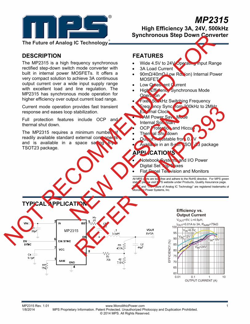
ORDERING INFORMATION Part Number* Package Top Marking
MP2315GJ TSOT23-8 AGC
* For Tape & Reel, add suffix –Z (e.g. MP2315GJ–Z);
PACKAGE REFERENCE
AAM
IN
SW
GND
FB
VCC
EN/SYNC
BST
1
2
3
4
8
7
6
5
TOP VIEW
TSOT23-8
ABSOLUTE MAXIMUM RATINGS (1) VIN ................................................–0.3V to +28V VSW........ –0.3V (-5V<10ns) to +28V (30V<10ns) VBST ........................................................ VSW+6V All Other Pins..................................-0.3V to +6V
Continuous Power Dissipation (TA=+25°C) (2)
... ................................................................. 1.25W Junction Temperature...............................150°C Lead Temperature ....................................260°C Storage Temperature................. -65°C to 150°C
Recommended Operating Conditions (3) Supply Voltage VIN ............................. 4.5 to 24V Output Voltage VOUT.................... 0.8V to VIN*DV Operating Junction Temp (TJ).. -40°C to +125°C
Thermal Resistance (4) θJA θJC TSOT23-8…………………...…….100…..55..°C/W
Notes: 1) Exceeding these ratings may damage the device. 2) The maximum allowable power dissipation is a function of the
maximum junction temperature TJ (MAX), the junction-to-ambient thermal resistance θJA, and the ambient temperature TA. The maximum allowable continuous power dissipation at any ambient temperature is calculated by PD (MAX) = (TJ
(MAX)-TA)/θJA. Exceeding the maximum allowable power dissipation will cause excessive die temperature, and the regulator will go into thermal shutdown. Internal thermal shutdown circuitry protects the device from permanent damage.
3) The device is not guaranteed to function outside of its operating conditions.
4) Measured on JESD51-7, 4-layer PCB.
NOT RECOMMENDED FOR
NEW D
ESIGNS
REFER TO MP23
93
MP2315 – 24V, 3A SYNC STEP DOWN CONVERTER
MP2315 Rev. 1.01 www.MonolithicPower.com 3 1/8/2014 MPS Proprietary Information. Patent Protected. Unauthorized Photocopy and Duplication Prohibited. © 2014 MPS. All Rights Reserved.
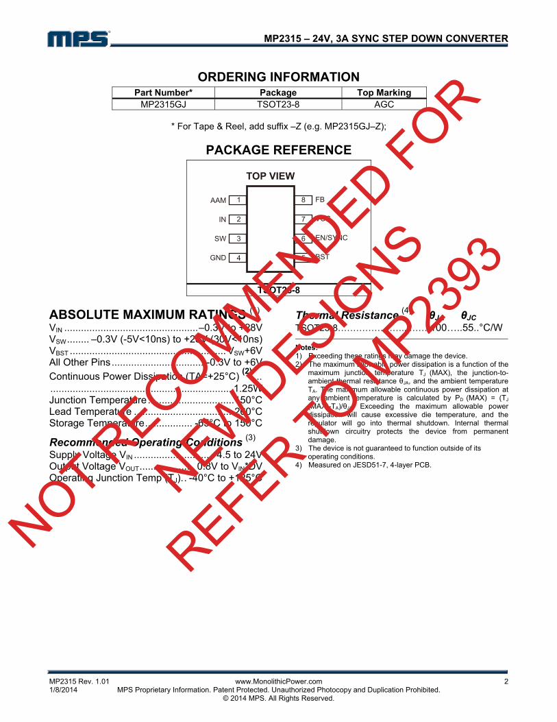
ELECTRICAL CHARACTERISTICS (5) VIN = 12V, TA = 25°C, unless otherwise noted.
Parameter Symbol Condition Min Typ Max Units
Supply Current (Shutdown) IIN VEN = 0V 1 μA
Supply Current (Quiescent) Iq VEN = 2V, VFB = 1V, AAM=0.5V
130 180 240 μA
HS Switch On Resistance HSRDS-ON VBST-SW=5V 90 mΩ
LS Switch On Resistance LSRDS-ON VCC=5V 40 mΩ
Switch Leakage SWLKG VEN = 0V, VSW =12V 1 μA
Current Limit ILIMIT Duty Cycle=40% 4.5 5.5 6.5 A
Oscillator Frequency fSW VFB=750mV 420 500 620 kHz
Fold-back Frequency fFB VFB=200mV 0.5 fSW
Maximum Duty Cycle DMAX VFB=750mV 90 95 %
Minimum On Time (5) TON_MIN 60 ns
Sync Frequency Range fSYNC 0.2 2 MHz
Feedback Voltage VFB TA=25ºC
779 791 803 mV
Feedback Current IFB VFB=820mV 10 50 nA
EN Rising Threshold VEN_RISING 1.2 1.4 1.6 V
EN Hysteresis VEN_HYS 80 150 220 mV
VEN=2V 1.5 2 2.5 μA EN Input Current IEN
VEN=0 0 50 nA
EN Turn Off Delay ENTd-off 6 10 14 μs
VIN Under Voltage Lockout Threshold-Rising
INUVVth 3.7 3.9 4.1 V
VIN Under Voltage Lockout Threshold-Hysteresis
INUVHYS 550 650 750 mV
VCC Regulator VCC 4.65 4.9 5.15 V
VCC Load Regulation ICC=5mA 0 1 3 %
Soft-Start Period TSS 10% to 90% 0.8 1.5 2.2 ms
Thermal Shutdown 150 ºC
Thermal Hysteresis 20 ºC
AAM Source Current IAAM 5.6 6.2 6.8 μA
Notes: 5) Guaranteed by design NOT R
ECOMMENDED FOR
NEW D
ESIGNS
REFER TO MP23
93
MP2315 – 24V, 3A SYNC STEP DOWN CONVERTER
MP2315 Rev. 1.01 www.MonolithicPower.com 4 1/8/2014 MPS Proprietary Information. Patent Protected. Unauthorized Photocopy and Duplication Prohibited. © 2014 MPS. All Rights Reserved.
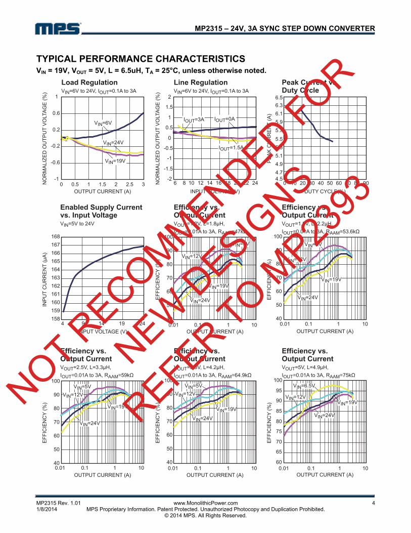
TYPICAL PERFORMANCE CHARACTERISTICS VIN = 19V, VOUT = 5V, L = 6.5uH, TA = 25°C, unless otherwise noted.
-1
-0.6
-0.2
0.2
0.6
1
0 0.5 1 1.5 2 2.5 3
Peak Current vs. Duty Cycle
-2
-1.5
-1
-0.5
0
0.5
1
1.5
2
6 8 10 12 14 16 18 20 22 24 0 10 20 30 40 50 60 70 80 90
158
159
160
161
162
163
164
165
166
167
168
4 9 14 19 2440
50
60
70
80
90
100
0.01 0.1 1 1040
50
60
70
80
90
100
0.01 0.1 1 10
40
50
60
70
80
90
100
0.01 0.1 1 1040
50
60
70
80
90
100
0.01 0.1 1 1060
65
70
75
80
85
90
95
100
0.01 0.1 1 10
4.54.7
4.9
5.1
5.3
5.5
5.7
5.9
6.1
6.3
6.5
NOT RECOMMENDED FOR
NEW D
ESIGNS
REFER TO MP23
93
MP2315 – 24V, 3A SYNC STEP DOWN CONVERTER
MP2315 Rev. 1.01 www.MonolithicPower.com 5 1/8/2014 MPS Proprietary Information. Patent Protected. Unauthorized Photocopy and Duplication Prohibited. © 2014 MPS. All Rights Reserved.
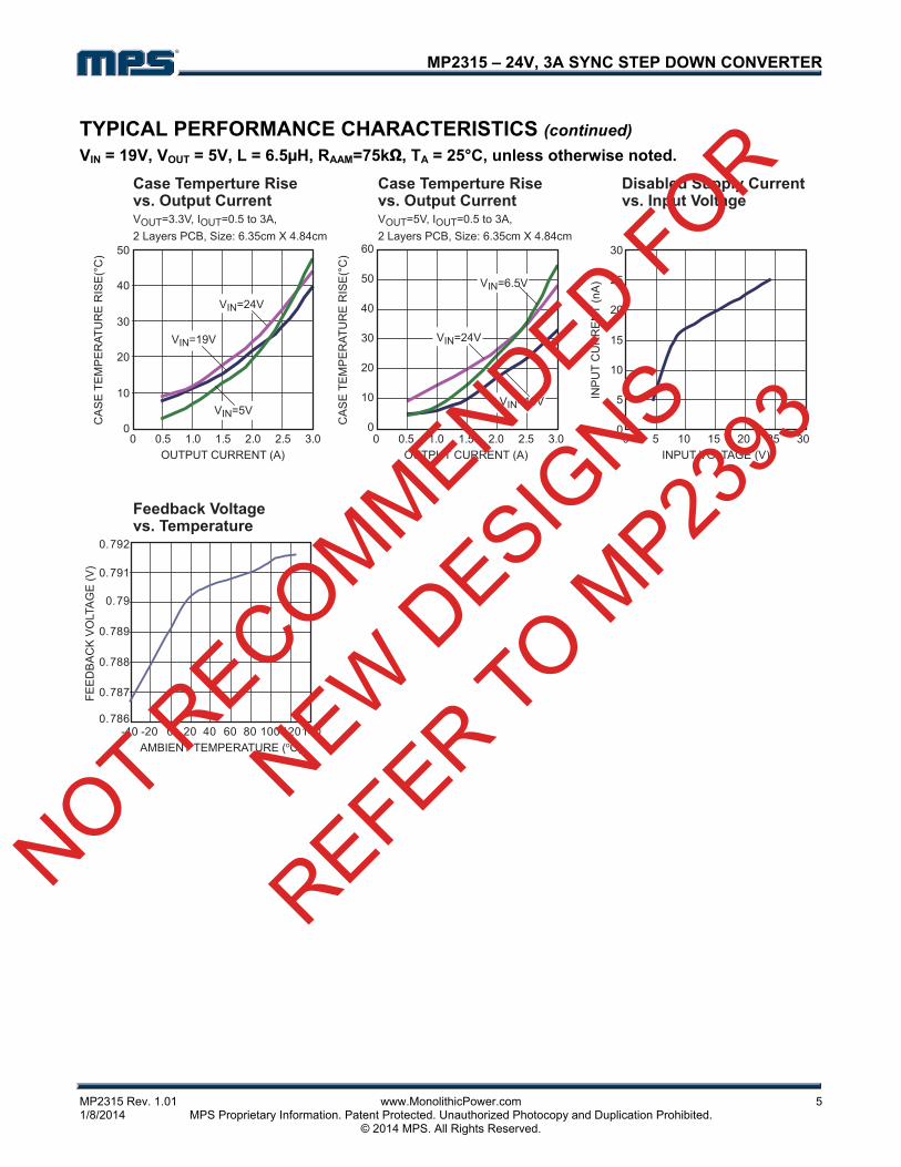
TYPICAL PERFORMANCE CHARACTERISTICS (continued) VIN = 19V, VOUT = 5V, L = 6.5µH, RAAM=75kΩ, TA = 25°C, unless otherwise noted.
0
10
20
30
40
50
0
10
20
30
40
60
50
0 0.5 1.0 1.5 2.0 2.5 3.0
Case Temperture Rise vs. Output CurrentVOUT=5V, IOUT=0.5 to 3A,
2 Layers PCB, Size: 6.35cm X 4.84cm
0 0.5 1.0 1.5 2.0 2.5 3.0
Case Temperture Rise vs. Output CurrentVOUT=3.3V, IOUT=0.5 to 3A,
2 Layers PCB, Size: 6.35cm X 4.84cm
Disabled Supply Current vs. Input Voltage
0
5
10
15
20
25
30
0 5 10 15 20 25 30
Feedback Voltage vs. Temperature
0.786
0.787
0.788
0.789
0.79
0.791
0.792
-40 -20 0 20 40 60 80 100120140
NOT RECOMMENDED FOR
NEW D
ESIGNS
REFER TO MP23
93
MP2315 – 24V, 3A SYNC STEP DOWN CONVERTER
MP2315 Rev. 1.01 www.MonolithicPower.com 6 1/8/2014 MPS Proprietary Information. Patent Protected. Unauthorized Photocopy and Duplication Prohibited. © 2014 MPS. All Rights Reserved.
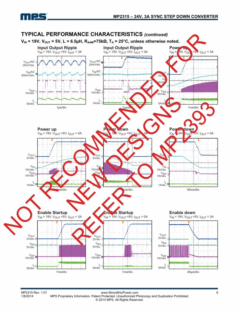
TYPICAL PERFORMANCE CHARACTERISTICS (continued) VIN = 19V, VOUT = 5V, L = 6.5µH, RAAM=75kΩ, TA = 25°C, unless otherwise noted.
VOUT/AC20mV/div.
VIN/AC500mV/div.
VSW10V/div.
IL5A/div.
VOUT/AC20mV/div.
VIN/AC500mV/div.
VSW10V/div.
IL1A/div.
VOUT2V/div.
VIN10V/div.
VSW10V/div.
IL1A/div.
VOUT2V/div.
VIN10V/div.
VSW10V/div.
IL5A/div.
VOUT2V/div.
VEN5V/div.
VSW10V/div.
IL5A/div.
VOUT2V/div.
VEN5V/div.
VSW10V/div.
IL5A/div.
VOUT2V/div.
VEN5V/div.
VSW10V/div.
IL5A/div.
VOUT2V/div.
VIN10V/div.
VSW10V/div.
IL5A/div.
VOUT2V/div.
VIN10V/div.
VSW10V/div.
IL1A/div.
NOT RECOMMENDED FOR
NEW D
ESIGNS
REFER TO MP23
93
MP2315 – 24V, 3A SYNC STEP DOWN CONVERTER
MP2315 Rev. 1.01 www.MonolithicPower.com 7 1/8/2014 MPS Proprietary Information. Patent Protected. Unauthorized Photocopy and Duplication Prohibited. © 2014 MPS. All Rights Reserved.
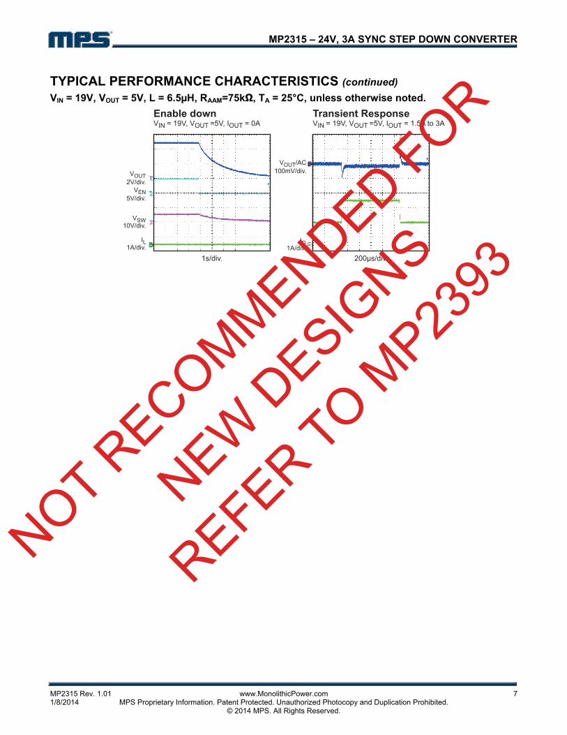
TYPICAL PERFORMANCE CHARACTERISTICS (continued) VIN = 19V, VOUT = 5V, L = 6.5µH, RAAM=75kΩ, TA = 25°C, unless otherwise noted.
VOUT/AC100mV/div.
IO1A/div.
VOUT2V/div.
VEN5V/div.
VSW10V/div.
IL1A/div.
NOT RECOMMENDED FOR
NEW D
ESIGNS
REFER TO MP23
93
MP2315 – 24V, 3A SYNC STEP DOWN CONVERTER
MP2315 Rev. 1.01 www.MonolithicPower.com 8 1/8/2014 MPS Proprietary Information. Patent Protected. Unauthorized Photocopy and Duplication Prohibited. © 2014 MPS. All Rights Reserved.
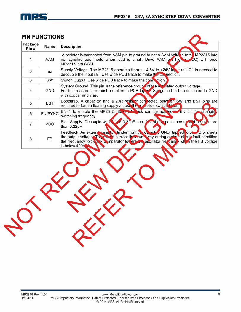
PIN FUNCTIONS Package
Pin # Name Description
1 AAM A resistor is connected from AAM pin to ground to set a AAM voltage force MP2315 into non-synchronous mode when load is small. Drive AAM pin high (=VCC) will force MP2315 into CCM.
2 IN Supply Voltage. The MP2315 operates from a +4.5V to +24V input rail. C1 is needed to decouple the input rail. Use wide PCB trace to make the connection.
3 SW Switch Output. Use wide PCB trace to make the connection.
4 GND System Ground. This pin is the reference ground of the regulated output voltage. For this reason care must be taken in PCB layout. Suggested to be connected to GND with copper and vias.
5 BST Bootstrap. A capacitor and a 20Ω resistor connected between SW and BST pins arerequired to form a floating supply across the high-side switch driver.
6 EN/SYNC EN=1 to enable the MP2315. External clock can be applied to EN pin for changing switching frequency.
7 VCC Bias Supply. Decouple with 0.1μF-0.22μF cap. And the capacitance should be no more than 0.22μF
8 FB
Feedback. An external resistor divider from the output to GND, tapped to the FB pin, sets the output voltage. To prevent current limit run away during a short circuit fault condition the frequency fold-back comparator lowers the oscillator frequency when the FB voltage is below 400mV.
NOT RECOMMENDED FOR
NEW D
ESIGNS
REFER TO MP23
93
MP2315 – 24V, 3A SYNC STEP DOWN CONVERTER
MP2315 Rev. 1.01 www.MonolithicPower.com 9 1/8/2014 MPS Proprietary Information. Patent Protected. Unauthorized Photocopy and Duplication Prohibited. © 2014 MPS. All Rights Reserved.
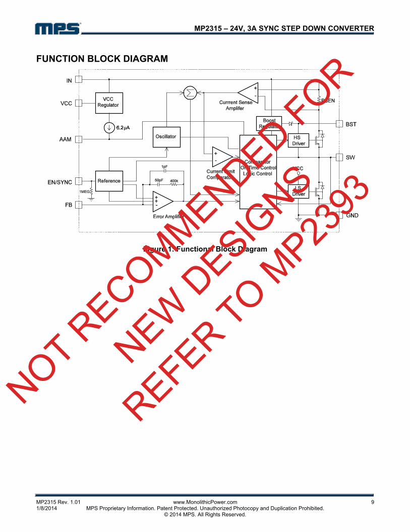
FUNCTION BLOCK DIAGRAM
Figure 1: Functional Block Diagram
NOT RECOMMENDED FOR
NEW D
ESIGNS
REFER TO MP23
93
MP2315 – 24V, 3A SYNC STEP DOWN CONVERTER
MP2315 Rev. 1.01 www.MonolithicPower.com 10 1/8/2014 MPS Proprietary Information. Patent Protected. Unauthorized Photocopy and Duplication Prohibited. © 2014 MPS. All Rights Reserved.
OPERATIONThe MP2315 is a high frequency synchronous rectified step-down switch mode converter with built in internal power MOSFETs. It offers a very compact solution to achieve 3A continuous output current over a wide input supply range with excellent load and line regulation.
The MP2315 operates in a fixed frequency, peak current control mode to regulate the output voltage. A PWM cycle is initiated by the internal clock. The integrated high-side power MOSFET is turned on and remains on until its current reaches the value set by the COMP voltage. When the power switch is off, it remains off until the next clock cycle starts. If, in 95% of one PWM period, the current in the power MOSFET does not reach the COMP set current value, the power MOSFET will be forced to turn off.
Internal Regulator Most of the internal circuitries are powered from the 5V internal regulator. This regulator takes the VIN input and operates in the full VIN range. When VIN is greater than 5.0V, the output of the regulator is in full regulation. When VIN is lower than 5.0V, the output decreases, a 0.1uF ceramic capacitor for decoupling purpose is required.
Error Amplifier The error amplifier compares the FB pin voltage with the internal 0.8V reference (REF) and outputs a COMP voltage, which is used to control the power MOSFET current. The optimized internal compensation network minimizes the external component counts and simplifies the control loop design.
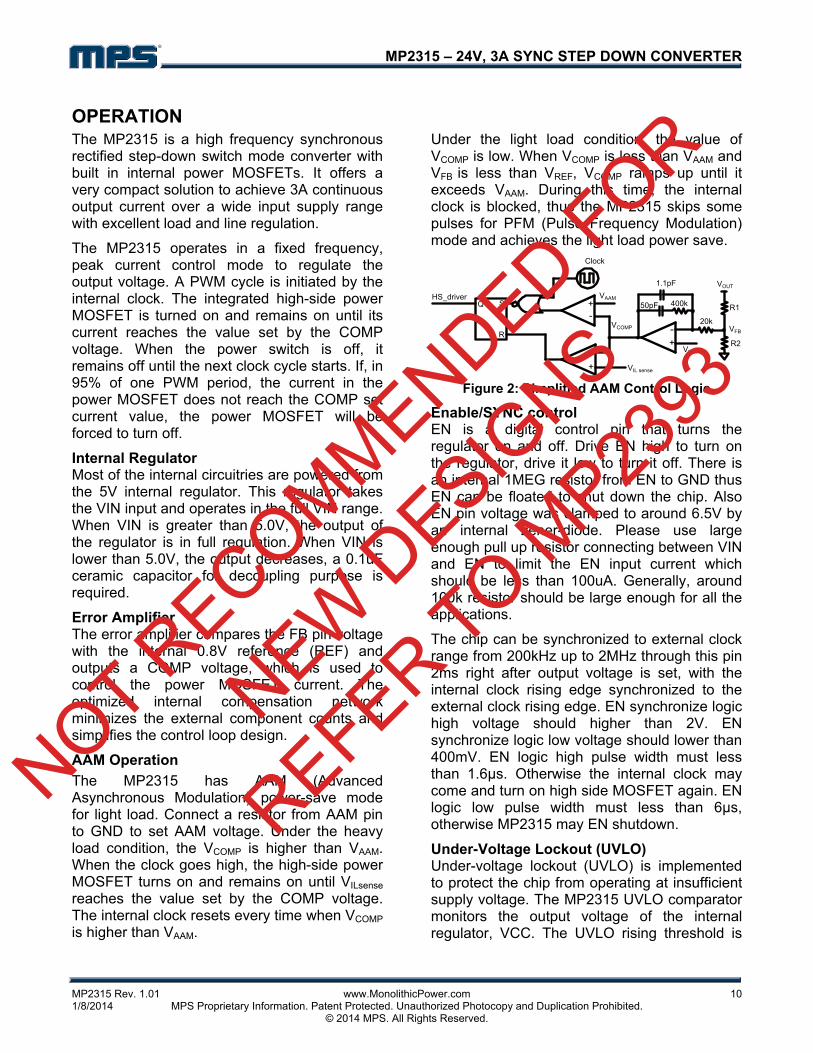
AAM Operation
The MP2315 has AAM (Advanced Asynchronous Modulation) power-save mode for light load. Connect a resistor from AAM pin to GND to set AAM voltage. Under the heavy load condition, the VCOMP is higher than VAAM. When the clock goes high, the high-side power MOSFET turns on and remains on until VILsense reaches the value set by the COMP voltage. The internal clock resets every time when VCOMP is higher than VAAM.
Under the light load condition, the value of VCOMP is low. When VCOMP is less than VAAM and VFB is less than VREF, VCOMP ramps up until it exceeds VAAM. During this time, the internal clock is blocked, thus the MP2315 skips some pulses for PFM (Pulse Frequency Modulation) mode and achieves the light load power save.
HS_driver
Clock
VAAM
VCOMP
VIL sense
VREF
VOUT
VFB
R1
R2
1.1pF
50pF 400k
20k
Q S
R
Figure 2: Simplified AAM Control Logic
Enable/SYNC control EN is a digital control pin that turns the regulator on and off. Drive EN high to turn on the regulator, drive it low to turn it off. There is an internal 1MEG resistor from EN to GND thus EN can be floated to shut down the chip. Also EN pin voltage was clamped to around 6.5V by an internal zener-diode. Please use large enough pull up resistor connecting between VIN and EN to limit the EN input current which should be less than 100uA. Generally, around 100k resistor should be large enough for all the applications.
The chip can be synchronized to external clock range from 200kHz up to 2MHz through this pin 2ms right after output voltage is set, with the internal clock rising edge synchronized to the external clock rising edge. EN synchronize logic high voltage should higher than 2V. EN synchronize logic low voltage should lower than 400mV. EN logic high pulse width must less than 1.6µs. Otherwise the internal clock may come and turn on high side MOSFET again. EN logic low pulse width must less than 6µs, otherwise MP2315 may EN shutdown.
Under-Voltage Lockout (UVLO) Under-voltage lockout (UVLO) is implemented to protect the chip from operating at insufficient supply voltage. The MP2315 UVLO comparator monitors the output voltage of the internal regulator, VCC. The UVLO rising threshold is
NOT RECOMMENDED FOR
NEW D
ESIGNS
REFER TO MP23
93
MP2315 – 24V, 3A SYNC STEP DOWN CONVERTER
MP2315 Rev. 1.01 www.MonolithicPower.com 11 1/8/2014 MPS Proprietary Information. Patent Protected. Unauthorized Photocopy and Duplication Prohibited. © 2014 MPS. All Rights Reserved.
about 3.9V while its falling threshold is consistent 3.25V.
Internal Soft-Start The soft start is implemented to prevent the converter output voltage from overshooting during start up. When the chip starts, the internal circuitry generates a soft-start voltage (SS) ramping up from 0V. The soft-start period lasts until the voltage on the soft-start capacitor exceeds the reference voltage of 0.8V. At this point the reference voltage takes over. The soft-start time is internally set to be around 1.5ms.
Over-Current-Protection and Hiccup The MP2315 has cycle-by-cycle over current limit when the inductor current peak value exceeds the set current limit threshold. Meanwhile, output voltage starts to drop until FB is below the Under-Voltage (UV) threshold, typically 50% below the reference. Once a UV is triggered, the MP2315 enters hiccup mode to periodically restart the part. This protection mode is especially useful when the output is dead-short to ground. The average short circuit current is greatly reduced to alleviate the thermal issue and to protect the regulator. The MP2315 exits the hiccup mode once the over current condition is removed.
Thermal Shutdown Thermal shutdown is implemented to prevent the chip from operating at exceedingly high temperatures. When the silicon die temperature is higher than 150°C, it shuts down the whole chip. When the temperature is lower than its lower threshold, typically 130°C, the chip is enabled again.
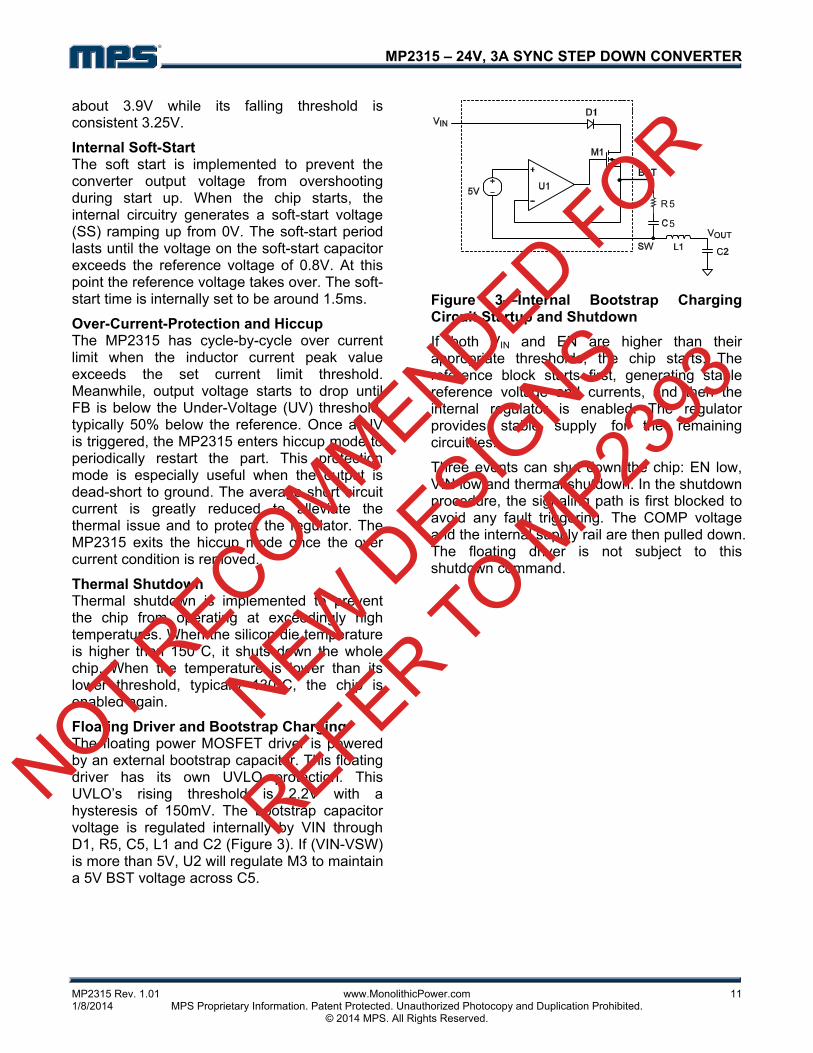
Floating Driver and Bootstrap Charging The floating power MOSFET driver is powered by an external bootstrap capacitor. This floating driver has its own UVLO protection. This UVLO’s rising threshold is 2.2V with a hysteresis of 150mV. The bootstrap capacitor voltage is regulated internally by VIN through D1, R5, C5, L1 and C2 (Figure 3). If (VIN-VSW) is more than 5V, U2 will regulate M3 to maintain a 5V BST voltage across C5.
5
R 5
Figure 3—Internal Bootstrap Charging Circuit Startup and Shutdown
If both VIN and EN are higher than their appropriate thresholds, the chip starts. The reference block starts first, generating stable reference voltage and currents, and then the internal regulator is enabled. The regulator provides stable supply for the remaining circuitries.
Three events can shut down the chip: EN low, VIN low and thermal shutdown. In the shutdown procedure, the signaling path is first blocked to avoid any fault triggering. The COMP voltage and the internal supply rail are then pulled down. The floating driver is not subject to this shutdown command.
NOT RECOMMENDED FOR
NEW D
ESIGNS
REFER TO MP23
93
MP2315 – 24V, 3A SYNC STEP DOWN CONVERTER
MP2315 Rev. 1.01 www.MonolithicPower.com 12 1/8/2014 MPS Proprietary Information. Patent Protected. Unauthorized Photocopy and Duplication Prohibited. © 2014 MPS. All Rights Reserved.
APPLICATION INFORMATIONCOMPONENT SELECTION
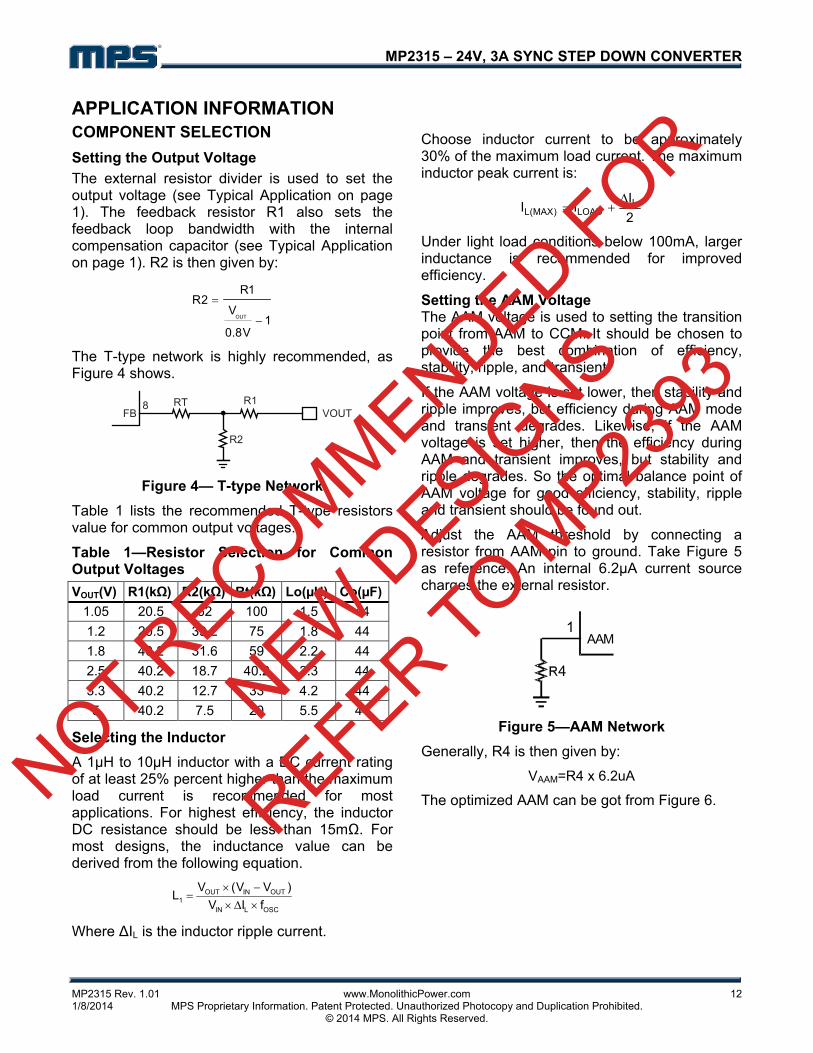
Setting the Output Voltage
The external resistor divider is used to set the output voltage (see Typical Application on page 1). The feedback resistor R1 also sets the feedback loop bandwidth with the internal compensation capacitor (see Typical Application on page 1). R2 is then given by:
OUT
R1R2
V1
0.8V
The T-type network is highly recommended, as Figure 4 shows.
FB8 RT
R2
R1VOUT
Figure 4— T-type Network
Table 1 lists the recommended T-type resistors value for common output voltages.
Table 1—Resistor Selection for Common Output Voltages
VOUT(V) R1(kΩ) R2(kΩ) Rt(kΩ) Lo(µH) Co(µF)
1.05 20.5 62 100 1.5 44
1.2 20.5 39.2 75 1.8 44
1.8 40.2 31.6 59 2.2 44
2.5 40.2 18.7 40.2 3.3 44
3.3 40.2 12.7 33 4.2 44
5 40.2 7.5 20 5.5 44
Selecting the Inductor
A 1µH to 10µH inductor with a DC current rating of at least 25% percent higher than the maximum load current is recommended for most applications. For highest efficiency, the inductor DC resistance should be less than 15mΩ. For most designs, the inductance value can be derived from the following equation.
OUT IN OUT1
IN L OSC
V (V V )L
V I f
Where ΔIL is the inductor ripple current.
Choose inductor current to be approximately 30% of the maximum load current. The maximum inductor peak current is:
2
III LLOAD)MAX(L
Under light load conditions below 100mA, larger inductance is recommended for improved efficiency.
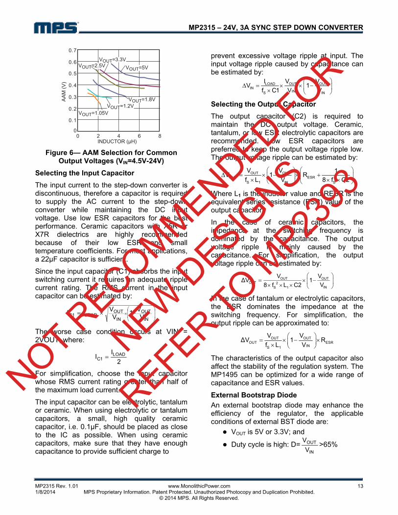
Setting the AAM Voltage The AAM voltage is used to setting the transition point from AAM to CCM. It should be chosen to provide the best combination of efficiency, stability, ripple, and transient.
If the AAM voltage is set lower, then stability and ripple improves, but efficiency during AAM mode and transient degrades. Likewise, if the AAM voltage is set higher, then the efficiency during AAM and transient improves, but stability and ripple degrades. So the optimal balance point of AAM voltage for good efficiency, stability, ripple and transient should be found out.
Adjust the AAM threshold by connecting a resistor from AAM pin to ground. Take Figure 5 as reference. An internal 6.2µA current source charges the external resistor.
AAM
4
1
Figure 5—AAM Network
Generally, R4 is then given by:
VAAM=R4 x 6.2uA
The optimized AAM can be got from Figure 6. NOT RECOMMENDED FOR
NEW D
ESIGNS
REFER TO MP23
93
MP2315 – 24V, 3A SYNC STEP DOWN CONVERTER
MP2315 Rev. 1.01 www.MonolithicPower.com 13 1/8/2014 MPS Proprietary Information. Patent Protected. Unauthorized Photocopy and Duplication Prohibited. © 2014 MPS. All Rights Reserved.
0
0.1
0.2
0.3
0.4
0.5
0.6
0.7
0 2 4 6 8
Figure 6— AAM Selection for Common Output Voltages (VIN=4.5V-24V)
Selecting the Input Capacitor
The input current to the step-down converter is discontinuous, therefore a capacitor is required to supply the AC current to the step-down converter while maintaining the DC input voltage. Use low ESR capacitors for the best performance. Ceramic capacitors with X5R or X7R dielectrics are highly recommended because of their low ESR and small temperature coefficients. For most applications, a 22µF capacitor is sufficient.
Since the input capacitor (C1) absorbs the input switching current it requires an adequate ripple current rating. The RMS current in the input capacitor can be estimated by:
IN
OUT
IN
OUTLOAD1C V
V1V
VII
The worse case condition occurs at VIN = 2VOUT, where:
2
II LOAD
1C
For simplification, choose the input capacitor whose RMS current rating greater than half of the maximum load current.
The input capacitor can be electrolytic, tantalum or ceramic. When using electrolytic or tantalum capacitors, a small, high quality ceramic capacitor, i.e. 0.1μF, should be placed as close to the IC as possible. When using ceramic capacitors, make sure that they have enough capacitance to provide sufficient charge to
prevent excessive voltage ripple at input. The input voltage ripple caused by capacitance can be estimated by:
LOAD OUT OUTIN
INS IN
I V VV 1
f C1 V V
Selecting the Output Capacitor
The output capacitor (C2) is required to maintain the DC output voltage. Ceramic, tantalum, or low ESR electrolytic capacitors are recommended. Low ESR capacitors are preferred to keep the output voltage ripple low. The output voltage ripple can be estimated by:
OUT OUTOUT ESR
S 1 IN S
V V 1V 1 R
f L V 8 f C2
Where L1 is the inductor value and RESR is the equivalent series resistance (ESR) value of the output capacitor.
In the case of ceramic capacitors, the impedance at the switching frequency is dominated by the capacitance. The output voltage ripple is mainly caused by the capacitance. For simplification, the output voltage ripple can be estimated by:
OUT OUTOUT 2
INS 1
V VΔV 1
V8 f L C2
In the case of tantalum or electrolytic capacitors, the ESR dominates the impedance at the switching frequency. For simplification, the output ripple can be approximated to:
OUT OUTOUT ESR
INS 1
V VΔV 1 R
f L V
The characteristics of the output capacitor also affect the stability of the regulation system. The MP1495 can be optimized for a wide range of capacitance and ESR values.
External Bootstrap Diode
An external bootstrap diode may enhance the efficiency of the regulator, the applicable conditions of external BST diode are:
VOUT is 5V or 3.3V; and
Duty cycle is high: D=IN
OUT
V
V>65%
NOT RECOMMENDED FOR
NEW D
ESIGNS
REFER TO MP23
93
MP2315 – 24V, 3A SYNC STEP DOWN CONVERTER
MP2315 Rev. 1.01 www.MonolithicPower.com 14 1/8/2014 MPS Proprietary Information. Patent Protected. Unauthorized Photocopy and Duplication Prohibited. © 2014 MPS. All Rights Reserved.
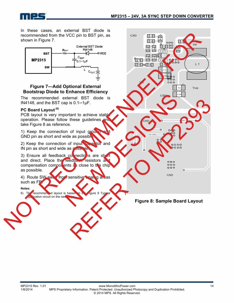
In these cases, an external BST diode is recommended from the VCC pin to BST pin, as shown in Figure 7.
RBST
5
Figure 7—Add Optional External Bootstrap Diode to Enhance Efficiency
The recommended external BST diode is IN4148, and the BST cap is 0.11μF.
PC Board Layout (6) PCB layout is very important to achieve stable operation. Please follow these guidelines and take Figure 8 as reference.
1) Keep the connection of input ground and GND pin as short and wide as possible.
2) Keep the connection of input capacitor and IN pin as short and wide as possible.
3) Ensure all feedback connections are short and direct. Place the feedback resistors and compensation components as close to the chip as possible.
4) Route SW away from sensitive analog areas such as FB.
Notes:
6) The recommended layout is based on the Figure 9 Typical Application circuit on the next page.
1
8 7 6
L 1
C 2
C 2A
C 1
R6R7
R8
R9
R4
R1
R2
R3
R5
C3
C5
C6
C4
1 2 3 4
Vin
GND
Vout
SW
GND
5
8C
C 1
A
SW
BST
EN / SYNC
VCC
GND
GND VOUT
Figure 8: Sample Board Layout
NOT RECOMMENDED FOR
NEW D
ESIGNS
REFER TO MP23
93
MP2315 – 24V, 3A SYNC STEP DOWN CONVERTER
MP2315 Rev. 1.01 www.MonolithicPower.com 15 1/8/2014 MPS Proprietary Information. Patent Protected. Unauthorized Photocopy and Duplication Prohibited. © 2014 MPS. All Rights Reserved.
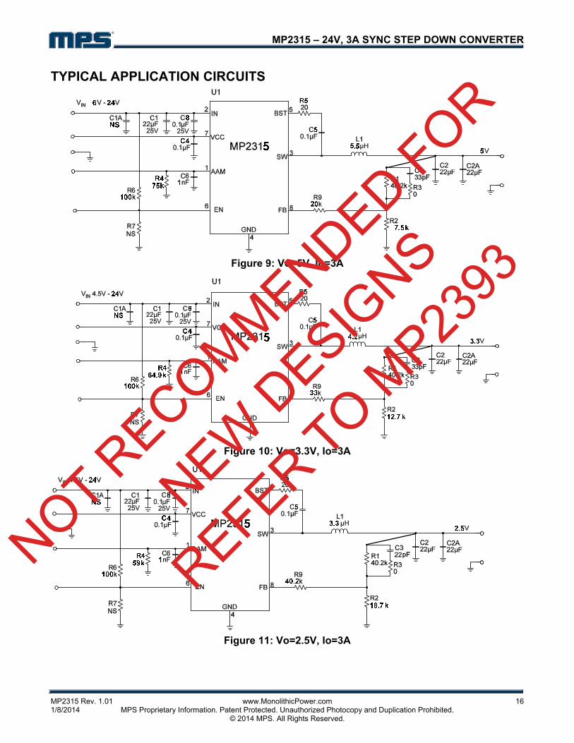
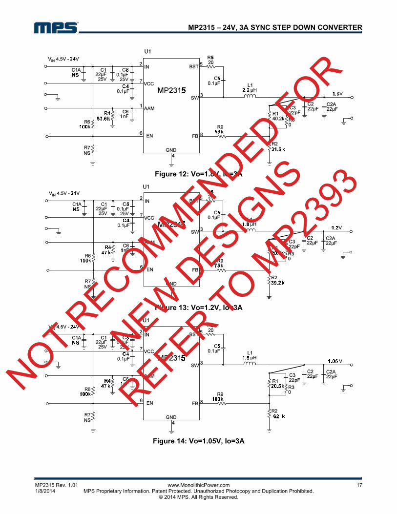
Design Example
Below is a design example following the application guidelines for the specifications:
Table 2: Design Example
VIN 19V VOUT 5V
IO 3A
The detailed application schematics are shown in Figures 9 through 14. The typical performance and circuit waveforms have been shown in the Typical Performance Characteristics section. For more device applications, please refer to the related Evaluation Board Datasheets.
NOT RECOMMENDED FOR
NEW D
ESIGNS
REFER TO MP23
93
MP2315 – 24V, 3A SYNC STEP DOWN CONVERTER
MP2315 Rev. 1.01 www.MonolithicPower.com 16 1/8/2014 MPS Proprietary Information. Patent Protected. Unauthorized Photocopy and Duplication Prohibited. © 2014 MPS. All Rights Reserved.
TYPICAL APPLICATION CIRCUITS
Figure 9: Vo=5V, Io=3A
Figure 10: Vo=3.3V, Io=3A
Figure 11: Vo=2.5V, Io=3A
NOT RECOMMENDED FOR
NEW D
ESIGNS
REFER TO MP23
93
MP2315 – 24V, 3A SYNC STEP DOWN CONVERTER
MP2315 Rev. 1.01 www.MonolithicPower.com 17 1/8/2014 MPS Proprietary Information. Patent Protected. Unauthorized Photocopy and Duplication Prohibited. © 2014 MPS. All Rights Reserved.
Figure 12: Vo=1.8V, Io=3A
Figure 13: Vo=1.2V, Io=3A
Figure 14: Vo=1.05V, Io=3A
NOT RECOMMENDED FOR
NEW D
ESIGNS
REFER TO MP23
93
MP2315 – 24V, 3A SYNC STEP DOWN CONVERTER
NOTICE: The information in this document is subject to change without notice. Users should warrant and guarantee that third party Intellectual Property rights are not infringed upon when integrating MPS products into any application. MPS will not assume any legal responsibility for any said applications.
MP2315 Rev. 1.01 www.MonolithicPower.com 18 1/8/2014 MPS Proprietary Information. Patent Protected. Unauthorized Photocopy and Duplication Prohibited. © 2014 MPS. All Rights Reserved.
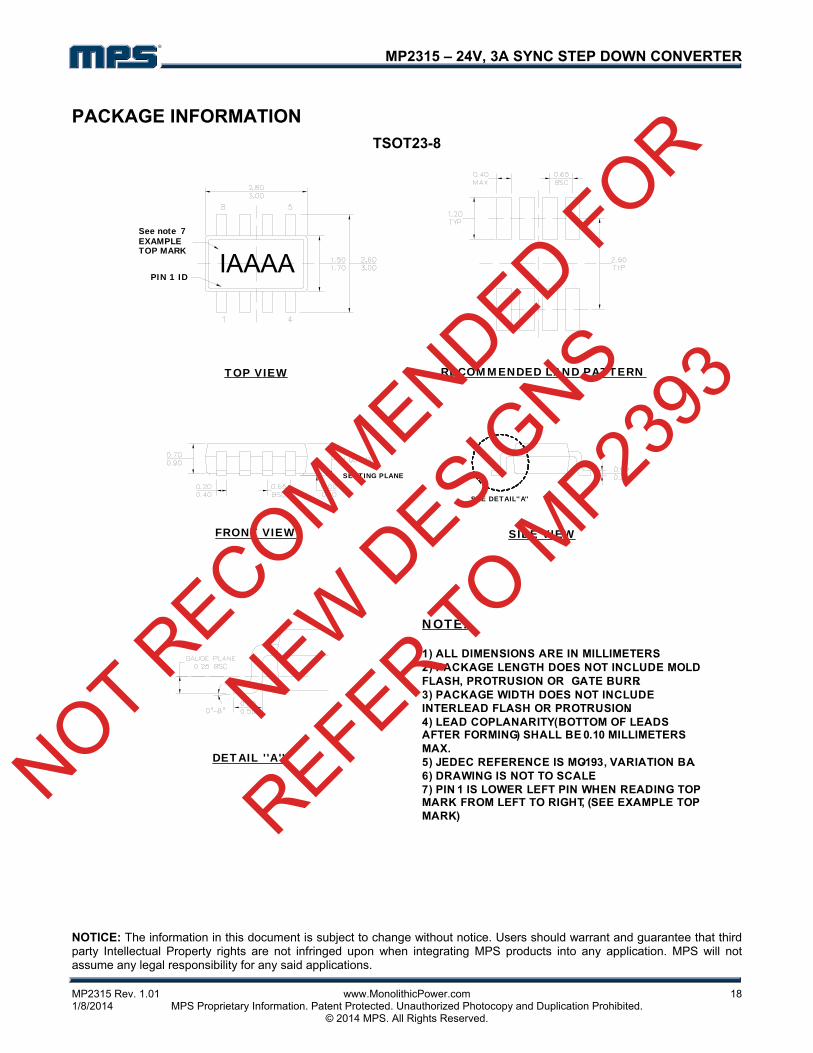
PACKAGE INFORMATION TSOT23-8
FRONT VIEW
NOTE:
1) ALL DIMENSIONS ARE IN MILLIMETERS.2) PACKAGE LENGTH DOES NOT INCLUDE MOLD FLASH, PROTRUSION OR GATE BURR.3) PACKAGE WIDTH DOES NOT INCLUDE INTERLEAD FLASH OR PROTRUSION.4) LEAD COPLANARITY (BOTTOM OF LEADS AFTER FORMING) SHALL BE 0.10 MILLIMETERS MAX.5) JEDEC REFERENCE IS MO-193, VARIATION BA.6) DRAWING IS NOT TO SCALE.7) PIN 1 IS LOWER LEFT PIN WHEN READING TOP MARK FROM LEFT TO RIGHT, (SEE EXAMPLE TOP MARK)
TOP VIEW RECOMMENDED LAND PATTERN
SEATING PLANE
SIDE VIEW
DETAIL ''A''
SEE DETAIL ''A''
IAAAAPIN 1 ID
See note 7EXAMPLE TOP MARK
NOT RECOMMENDED FOR
NEW D
ESIGNS
REFER TO MP23
93
Related Documents