HITK/ECE 1 M. Tech. in Electronics & Communication Engineering – VLSI (ECE-VLSI)

Welcome message from author
This document is posted to help you gain knowledge. Please leave a comment to let me know what you think about it! Share it to your friends and learn new things together.
Transcript
HITK/ECE 1
M. Tech. in Electronics & Communication Engineering – VLSI (ECE-VLSI)
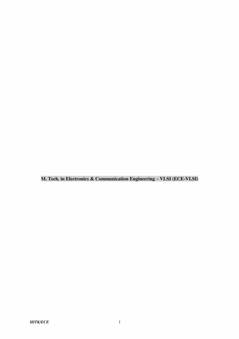
Curricular Structure
M.Tech. - ECE (Microelectronics & VLSI Design)
First Year, First Semester
A. Theory
Sl.
No.
Course
Code
Course Name Contact Hours/Week Credit
Points L T P Total
1 MATH5103 Advanced Mathematics 4 0 0 4 4
2 VLSI5101 VLSI Device & Modelling 4 0 0 4 4
3 VLSI5102 Digital IC Design 4 0 0 4 4
4 VLSI5103 Microelectronic Technology & IC
Fabrication 4 0 0 4 4
5
Elective – I
4 0 0 4 4 VLSI5131
Embedded Systems
VLSI5132 Digital Communication
Technology
Total Theory 20 20
B. Practical
6 VLSI5111 VLSI Frontend Design & CAD
Tools 0 0 3 3 2
7 VLSI5112 VLSI Backend Design &
Technology CAD Tools 0 0 3 3 2
Total Practical 6 4
C. Sessional
8 VLSI5121 Seminar 0 2 0 2 1
Total Sessional 2 1
Total of Semester 28 25
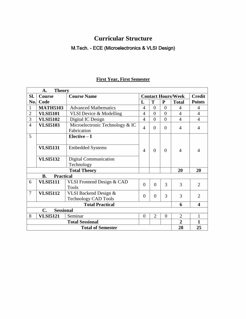
Second Semester
A. Theory
Sl.
No.
Course
Code
Course Name Contact Hours/Week Credit
Points L T P Total
1 VLSI5201 VLSI Processor Architecture 4 0 0 4 4
2 VLSI5202 VLSI Design, Verification and
Testing 4 0 0 4 4
3 VLSI5203 Analog IC Design 4 0 0 4 4
4 Elective – II
4 0 0 4 4 VLSI5231 Advanced Micro & Nano Devices
VLSI5232 DSP Algorithms for VLSI System
Design
5 Elective - III
4 0 0 4 4 VLSI5241 Low Power VLSI Circuit and
System
VLSI5242 Sensors
Total Theory 20 20
B. Practical
6 VLSI5213 Analog VLSI Design Laboratory 0 0 3 3 2
Total of practical 3 2
C. Sessional
7 VLSI5221 Term paper leading to thesis 0 4 0 4 3
Total Sessional 4 3
Total of Semester 27 25
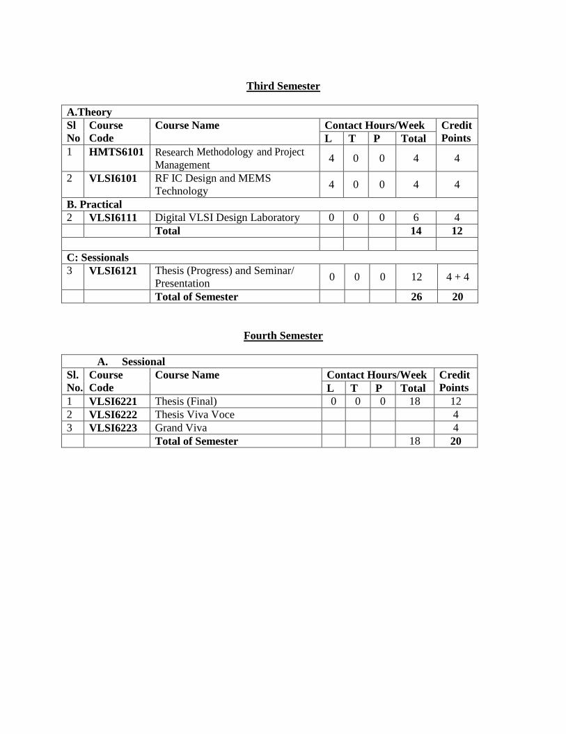
Third Semester
A.Theory
Sl
No
Course
Code
Course Name Contact Hours/Week Credit
Points L T P Total
1 HMTS6101 Research Methodology and Project
Management 4 0 0 4 4
2 VLSI6101 RF IC Design and MEMS
Technology 4 0 0 4 4
B. Practical
2 VLSI6111 Digital VLSI Design Laboratory 0 0 0 6 4
Total 14 12
C: Sessionals
3 VLSI6121 Thesis (Progress) and Seminar/
Presentation 0 0 0 12 4 + 4
Total of Semester 26 20
Fourth Semester
A. Sessional
Sl.
No.
Course
Code
Course Name Contact Hours/Week Credit
Points L T P Total
1 VLSI6221 Thesis (Final) 0 0 0 18 12
2 VLSI6222 Thesis Viva Voce 4
3 VLSI6223 Grand Viva 4
Total of Semester 18 20
HITK/ECE 5
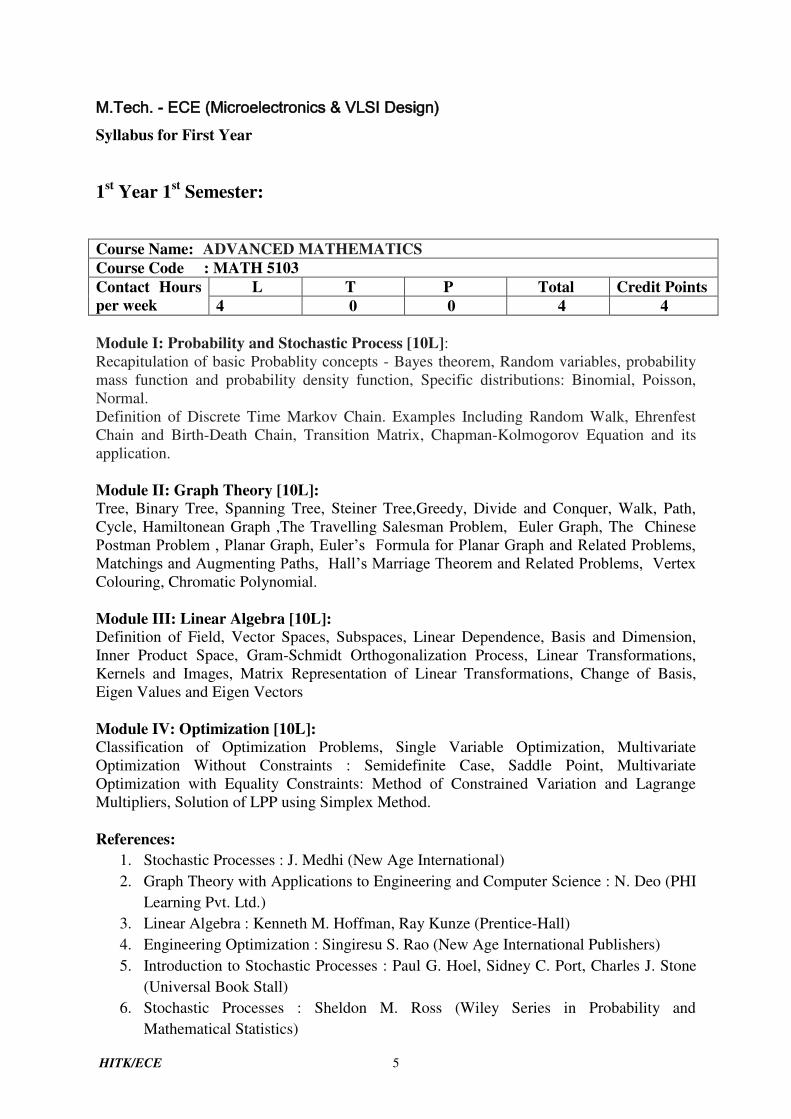
M.Tech. - ECE (Microelectronics & VLSI Design)
Syllabus for First Year
1st Year 1
st Semester:
Course Name: ADVANCED MATHEMATICS Course Code : MATH 5103
Contact Hours
per week
L T P Total Credit Points
4 0 0 4 4
Module I: Probability and Stochastic Process [10L]:
Recapitulation of basic Probablity concepts - Bayes theorem, Random variables, probability
mass function and probability density function, Specific distributions: Binomial, Poisson,
Normal.
Definition of Discrete Time Markov Chain. Examples Including Random Walk, Ehrenfest
Chain and Birth-Death Chain, Transition Matrix, Chapman-Kolmogorov Equation and its
application.
Module II: Graph Theory [10L]: Tree, Binary Tree, Spanning Tree, Steiner Tree,Greedy, Divide and Conquer, Walk, Path,
Cycle, Hamiltonean Graph ,The Travelling Salesman Problem, Euler Graph, The Chinese
Postman Problem , Planar Graph, Euler’s Formula for Planar Graph and Related Problems, Matchings and Augmenting Paths, Hall’s Marriage Theorem and Related Problems, Vertex Colouring, Chromatic Polynomial.
Module III: Linear Algebra [10L]: Definition of Field, Vector Spaces, Subspaces, Linear Dependence, Basis and Dimension,
Inner Product Space, Gram-Schmidt Orthogonalization Process, Linear Transformations,
Kernels and Images, Matrix Representation of Linear Transformations, Change of Basis,
Eigen Values and Eigen Vectors
Module IV: Optimization [10L]:
Classification of Optimization Problems, Single Variable Optimization, Multivariate
Optimization Without Constraints : Semidefinite Case, Saddle Point, Multivariate
Optimization with Equality Constraints: Method of Constrained Variation and Lagrange
Multipliers, Solution of LPP using Simplex Method.
References:
1. Stochastic Processes : J. Medhi (New Age International)
2. Graph Theory with Applications to Engineering and Computer Science : N. Deo (PHI
Learning Pvt. Ltd.)
3. Linear Algebra : Kenneth M. Hoffman, Ray Kunze (Prentice-Hall)
4. Engineering Optimization : Singiresu S. Rao (New Age International Publishers)
5. Introduction to Stochastic Processes : Paul G. Hoel, Sidney C. Port, Charles J. Stone
(Universal Book Stall)
6. Stochastic Processes : Sheldon M. Ross (Wiley Series in Probability and
Mathematical Statistics)
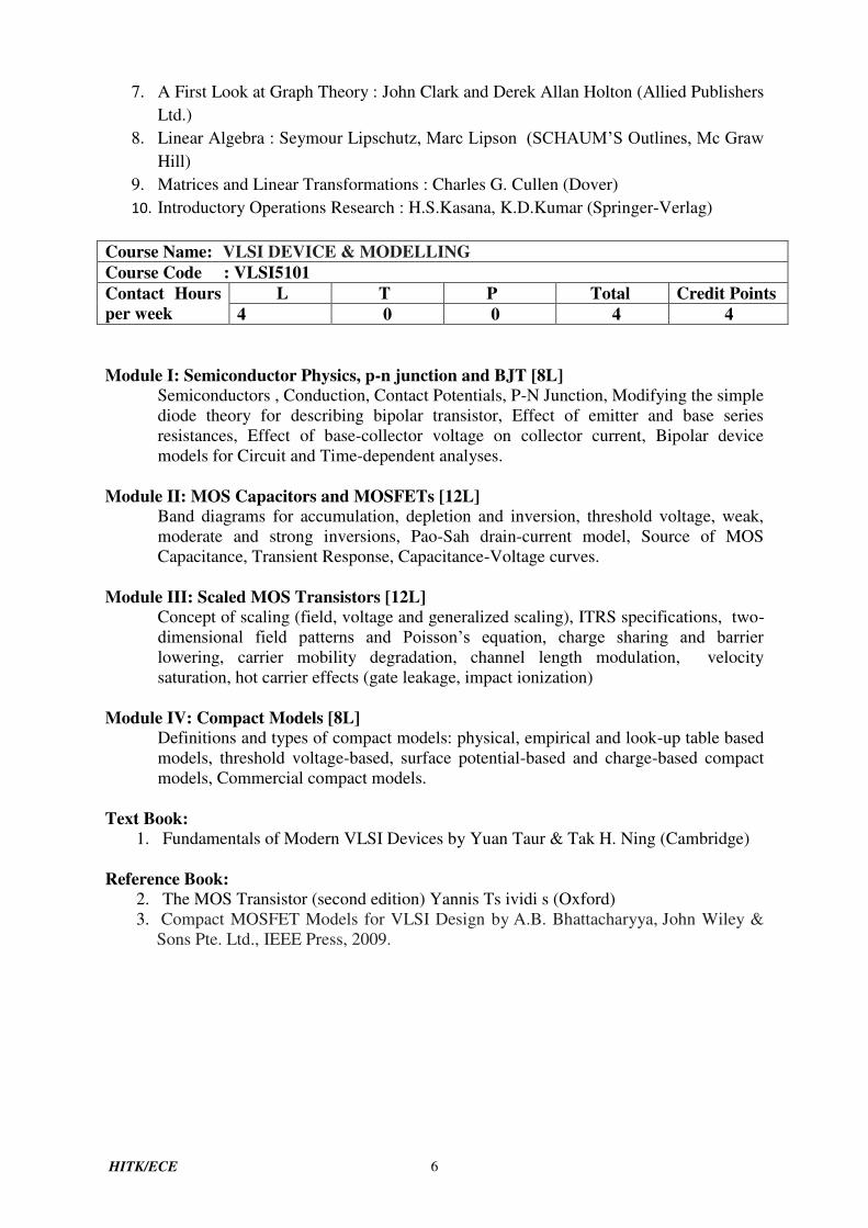
HITK/ECE 6
7. A First Look at Graph Theory : John Clark and Derek Allan Holton (Allied Publishers
Ltd.)
8. Linear Algebra : Seymour Lipschutz, Marc Lipson (SCHAUM’S Outlines, Mc Graw Hill)
9. Matrices and Linear Transformations : Charles G. Cullen (Dover)
10. Introductory Operations Research : H.S.Kasana, K.D.Kumar (Springer-Verlag)
Course Name: VLSI DEVICE & MODELLING Course Code : VLSI5101
Contact Hours
per week
L T P Total Credit Points
4 0 0 4 4
Module I: Semiconductor Physics, p-n junction and BJT [8L]
Semiconductors , Conduction, Contact Potentials, P-N Junction, Modifying the simple
diode theory for describing bipolar transistor, Effect of emitter and base series
resistances, Effect of base-collector voltage on collector current, Bipolar device
models for Circuit and Time-dependent analyses.
Module II: MOS Capacitors and MOSFETs [12L]
Band diagrams for accumulation, depletion and inversion, threshold voltage, weak,
moderate and strong inversions, Pao-Sah drain-current model, Source of MOS
Capacitance, Transient Response, Capacitance-Voltage curves.
Module III: Scaled MOS Transistors [12L]
Concept of scaling (field, voltage and generalized scaling), ITRS specifications, two-
dimensional field patterns and Poisson’s equation, charge sharing and barrier lowering, carrier mobility degradation, channel length modulation, velocity
saturation, hot carrier effects (gate leakage, impact ionization)
Module IV: Compact Models [8L]
Definitions and types of compact models: physical, empirical and look-up table based
models, threshold voltage-based, surface potential-based and charge-based compact
models, Commercial compact models.
Text Book:
1. Fundamentals of Modern VLSI Devices by Yuan Taur & Tak H. Ning (Cambridge)
Reference Book:
2. The MOS Transistor (second edition) Yannis Ts ividi s (Oxford)
3. Compact MOSFET Models for VLSI Design by A.B. Bhattacharyya, John Wiley &
Sons Pte. Ltd., IEEE Press, 2009.
HITK/ECE 7
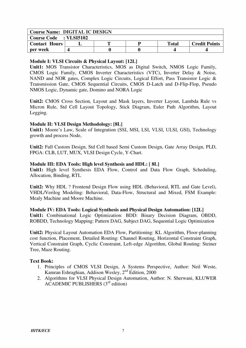
Course Name: DIGITAL IC DESIGN Course Code : VLSI5102
Contact Hours
per week
L T P Total Credit Points
4 0 0 4 4
Module I: VLSI Circuits & Physical Layout: [12L]
Unit1: MOS Transistor Characteristics, MOS as Digital Switch, NMOS Logic Family,
CMOS Logic Family, CMOS Inverter Characteristics (VTC), Inverter Delay & Noise,
NAND and NOR gates, Complex Logic Circuits, Logical Effort, Pass Transistor Logic &
Transmission Gate, CMOS Sequential Circuits, CMOS D-Latch and D-Flip-Flop, Pseudo
NMOS Logic, Dynamic gate, Domino and NORA Logic
Unit2: CMOS Cross Section, Layout and Mask layers, Inverter Layout, Lambda Rule vs
Micron Rule, Std Cell Layout Topology, Stick Diagram, Euler Path Algorithm, Layout
Legging.
Module II: VLSI Design Methodology: [8L] Unit1: Moore’s Law, Scale of Integration (SSI, MSI, LSI, VLSI, ULSI, GSI), Technology growth and process Node,
Unit2: Full Custom Design, Std Cell based Semi Custom Design, Gate Array Design, PLD,
FPGA: CLB, LUT, MUX, VLSI Design Cycle, Y-Chart.
Module III: EDA Tools: High level Synthesis and HDL: [ 8L]
Unit1: High level Synthesis EDA Flow, Control and Data Flow Graph, Scheduling,
Allocation, Binding, RTL
Unit2: Why HDL ? Frontend Design Flow using HDL (Behavioral, RTL and Gate Level),
VHDL/Verilog Modeling: Behavioral, Data-Flow, Structural and Mixed, FSM Example:
Mealy Machine and Moore Machine.
Module IV: EDA Tools: Logical Synthesis and Physical Design Automation: [12L]
Unit1: Combinational Logic Optimization: BDD: Binary Decision Diagram, OBDD,
ROBDD, Technology Mapping: Pattern DAG, Subject DAG, Sequential Logic Optimization
Unit2: Physical Layout Automation EDA Flow, Partitioning: KL Algorithm, Floor-planning
cost function, Placement, Detailed Routing: Channel Routing, Horizontal Constraint Graph,
Vertical Constraint Graph, Cyclic Constraint, Left-edge Algorithm, Global Routing: Steiner
Tree, Maze Routing.
Text Book:
1. Principles of CMOS VLSI Design, A Systems Perspective, Author: Neil Weste,
Kamran Eshraghian, Addison Wesley, 2nd
Edition, 2000
2. Algorithms for VLSI Physical Design Automation, Author: N. Sherwani, KLUWER
ACADEMIC PUBLISHERS (3rd
edition)
HITK/ECE 8
Reference Book:
3. CMOS Digital Integrated Circuits, Analysis and Design, Author: Sung-Mo Kang,
Yusuf Leblebici, Tata McGraw Hill (3rd
Edition), 2006
4. CMOS VLSI Design, A Circuits and Systems Perspective (3rd Edition) Author: Neil
Weste, David Harris, Ayan Banerjee. Pearson, 2011
5. Digital Integrated Circuit, Design Perspective, Author: .M. Rabaey, Prentice-Hall
6. VLSI Design and EDA TOOLS, Author: Angsuman Sarkar, Swapnadip De, Chandan
Kumar Sarkar, SCITECH PUBLICATIONS (India) Pvt. Ltd., 2011
7. Algorithms for VLSI Design Automation, Author: Gerez, Wiley, 2011
8. A VHDL Primer, J. Bhasker, Prentice-Hall, 2013
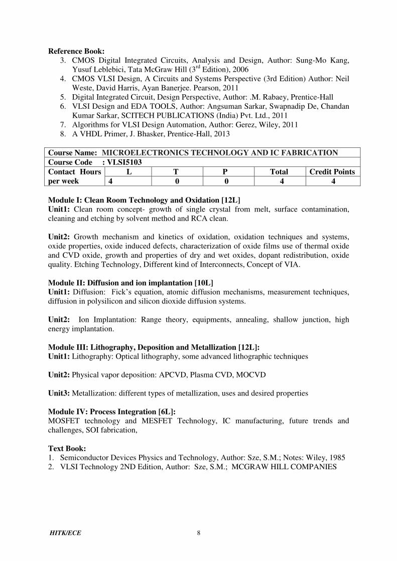
Course Name: MICROELECTRONICS TECHNOLOGY AND IC FABRICATION Course Code : VLSI5103
Contact Hours
per week
L T P Total Credit Points
4 0 0 4 4
Module I: Clean Room Technology and Oxidation [12L]
Unit1: Clean room concept- growth of single crystal from melt, surface contamination,
cleaning and etching by solvent method and RCA clean.
Unit2: Growth mechanism and kinetics of oxidation, oxidation techniques and systems,
oxide properties, oxide induced defects, characterization of oxide films use of thermal oxide
and CVD oxide, growth and properties of dry and wet oxides, dopant redistribution, oxide
quality. Etching Technology, Different kind of Interconnects, Concept of VIA.
Module II: Diffusion and ion implantation [10L]
Unit1: Diffusion: Fick’s equation, atomic diffusion mechanisms, measurement techniques, diffusion in polysilicon and silicon dioxide diffusion systems.
Unit2: Ion Implantation: Range theory, equipments, annealing, shallow junction, high
energy implantation.
Module III: Lithography, Deposition and Metallization [12L]: Unit1: Lithography: Optical lithography, some advanced lithographic techniques
Unit2: Physical vapor deposition: APCVD, Plasma CVD, MOCVD
Unit3: Metallization: different types of metallization, uses and desired properties
Module IV: Process Integration [6L]:
MOSFET technology and MESFET Technology, IC manufacturing, future trends and
challenges, SOI fabrication,
Text Book:
1. Semiconductor Devices Physics and Technology, Author: Sze, S.M.; Notes: Wiley, 1985
2. VLSI Technology 2ND Edition, Author: Sze, S.M.; MCGRAW HILL COMPANIES
HITK/ECE 9
Reference Book:
3. An Introduction to Semiconductor Microtechnology, Author: Morgan, D.V., and Board,
K
4. The National Technology Roadmap for Semiconductors , Notes: Semiconductors Industry
Association, SIA, 1994
5, Electrical and Electronic Engineering Series VLSI Technology, Author: Sze, S.M. Notes:
Mcgraw-Hill International Editions
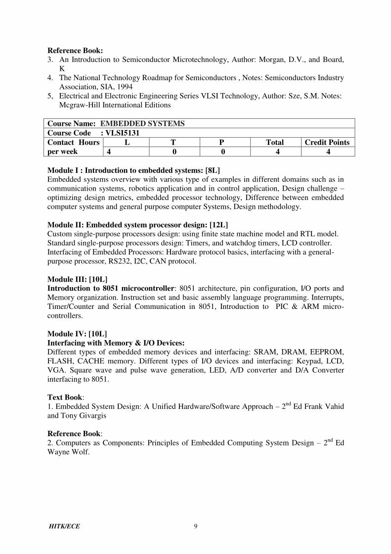
Course Name: EMBEDDED SYSTEMS Course Code : VLSI5131
Contact Hours
per week
L T P Total Credit Points
4 0 0 4 4
Module I : Introduction to embedded systems: [8L]
Embedded systems overview with various type of examples in different domains such as in
communication systems, robotics application and in control application, Design challenge –
optimizing design metrics, embedded processor technology, Difference between embedded
computer systems and general purpose computer Systems, Design methodology.
Module II: Embedded system processor design: [12L]
Custom single-purpose processors design: using finite state machine model and RTL model.
Standard single-purpose processors design: Timers, and watchdog timers, LCD controller.
Interfacing of Embedded Processors: Hardware protocol basics, interfacing with a general-
purpose processor, RS232, I2C, CAN protocol.
Module III: [10L]
Introduction to 8051 microcontroller: 8051 architecture, pin configuration, I/O ports and
Memory organization. Instruction set and basic assembly language programming. Interrupts,
Timer/Counter and Serial Communication in 8051, Introduction to PIC & ARM micro-
controllers.
Module IV: [10L]
Interfacing with Memory & I/O Devices:
Different types of embedded memory devices and interfacing: SRAM, DRAM, EEPROM,
FLASH, CACHE memory. Different types of I/O devices and interfacing: Keypad, LCD,
VGA. Square wave and pulse wave generation, LED, A/D converter and D/A Converter
interfacing to 8051.
Text Book:
1. Embedded System Design: A Unified Hardware/Software Approach – 2nd
Ed Frank Vahid
and Tony Givargis
Reference Book:
2. Computers as Components: Principles of Embedded Computing System Design – 2nd
Ed
Wayne Wolf.
HITK/ECE 10
Course Name: DIGITAL COMMUNICATION TECHNOLOGY Course Code : VLSI5132
Contact Hours
per week
L T P Total Credit Points
4 0 0 4 4
Module I: [10L]
Review of baseband digital signal transmission –PCM DM ADM ADPCM. Inter Symbol
Interference ( ISI ), Nyquist criteria for no ISI in band limited channel, Eye Diagram &
interpretation, Error Vector Magnitude, Error coding techniques, Viterbi decoding.
Parametric decoding: Sub band coding APC LPC voice excited vocoder
Synchronization – Symbol and Frame synchronization
Equalizer: Linear equalization Decision feedback equalizer iterative equalizer and decoding
Module II: [10L]
Digital Modulation:
Review of modulation schemes – BPSK DPSK QPSK M-ary PSK QASK MSK BFSK M-ary
FSK - principles transmitters receivers signal space presentation bandwidth efficiency
GMSK Orthogonal frequency division multiplexing ( OFDM ) – principle generation and
detection
Bit error performance of bandpass signal – Narrow band noise model Error performance
of different shift keying techniques like BPSK, Comparison of bandwidth efficiency and
error performance of modulation schemes
Module III: [9L]
Multiplexing and multiple access: TDM/TDMA FDM/FDMA Space DMA ALOHA –slotted ALOHA and reservation ALOHA CSMA-CD CSMA- CA basic techniques and
comparative performances
Spread spectrum modulation: Principle of DSS, processing gain jamming margin single
tone interference probability of error
Principle of frequency hopped spread spectrum (FHSS) – slow frequency and fast frequency
hopping
Principle of CDMA Multiple access interference (MAI) and limit of simultaneous users
Digital cellular CDMA system – forward and reverse link error rate performance
Module IV: [9L]
Optimum Detection and Estimation:
Noise vector in signal space Bayes detection of received signal, optimum M-ary receiver
design
Decision region and minimum error probability
Matched filter, Optimum detection of 16 QAM signal, MPSK signal orthogonal and bi
orthogonal signal
Decision criterion: maximum likelihood Neyman Pearson and Minimax decision criterion
Estimation: Linear estimation – simple mean Linear mean squared error Wiener filter
Non linear estimation: Bayes estimation MAP ML estimates
Text Book:
1. Digital Communications 4th edition J G Proakis MGH international Edition
HITK/ECE 11
Reference Book:
2. Principle of Communication Systems Taub and Schilling 7th edition TMH
3. Digital Communications :Fundamentals and Applications 2nd edn 2008 Bernard Sklar and
Pabitra Kumar Ray Pearson Education
4. Principle of Digital Communications Simon Haykin Wiley Student Edition
5. Digital Communications Zeimer and Tranter CRC Press
6. Wireless Communication & Networks: 3G & Beyond Iti Saha Mishra, McGraw-Hill
Education, 2nd
Edition
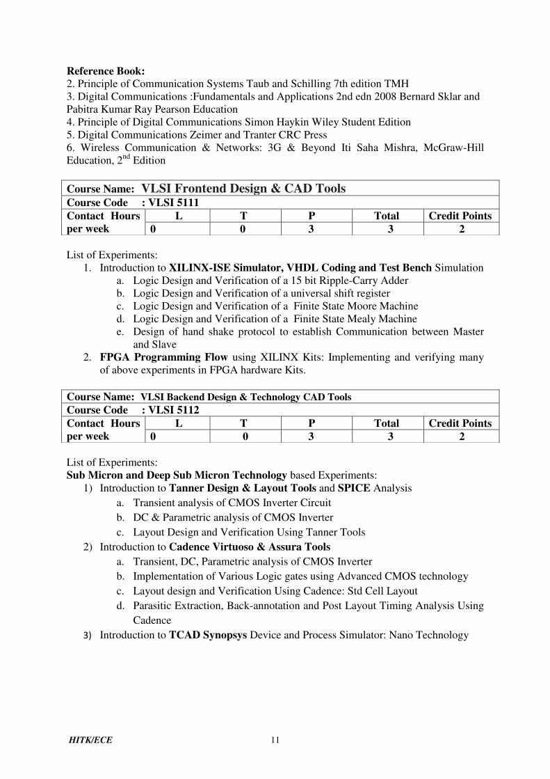
List of Experiments:
1. Introduction to XILINX-ISE Simulator, VHDL Coding and Test Bench Simulation
a. Logic Design and Verification of a 15 bit Ripple-Carry Adder
b. Logic Design and Verification of a universal shift register
c. Logic Design and Verification of a Finite State Moore Machine
d. Logic Design and Verification of a Finite State Mealy Machine
e. Design of hand shake protocol to establish Communication between Master
and Slave
2. FPGA Programming Flow using XILINX Kits: Implementing and verifying many
of above experiments in FPGA hardware Kits.
List of Experiments:
Sub Micron and Deep Sub Micron Technology based Experiments:
1) Introduction to Tanner Design & Layout Tools and SPICE Analysis
a. Transient analysis of CMOS Inverter Circuit
b. DC & Parametric analysis of CMOS Inverter
c. Layout Design and Verification Using Tanner Tools
2) Introduction to Cadence Virtuoso & Assura Tools
a. Transient, DC, Parametric analysis of CMOS Inverter
b. Implementation of Various Logic gates using Advanced CMOS technology
c. Layout design and Verification Using Cadence: Std Cell Layout
d. Parasitic Extraction, Back-annotation and Post Layout Timing Analysis Using
Cadence
3) Introduction to TCAD Synopsys Device and Process Simulator: Nano Technology
Course Name: VLSI Frontend Design & CAD Tools
Course Code : VLSI 5111
Contact Hours
per week
L T P Total Credit Points
0 0 3 3 2
Course Name: VLSI Backend Design & Technology CAD Tools Course Code : VLSI 5112
Contact Hours
per week
L T P Total Credit Points
0 0 3 3 2
HITK/ECE 12
1st Year 2
nd Semester:
Course Name: VLSI PROCESSOR ARCHITECTURE Course Code : VLSI5201
Contact Hours
per week
L T P Total Credit Points
4 0 0 4 4
Module I: Fundamentals: [8L]
Architecture organization, basic structure of instruction set architecture (ISA arch) and
Flynn’s taxonomy. Comparison of Von-Neumann and Harvard architecture, Microcoded and
hardwired control architecture, scalar and Vector processors architecture, CISC and RISC
architecture. Basic of pipelining, pipeline hazards and solutions.
Module II: The DSP and Its Impact on Technology: [12L]
Parallel computation using superscalar architecture, description of the very long Instruction
word architecture (VLIW arch) , detail description of TI TMS320C5x DSP processor
architecture.
Module III: Accelerator :[10L]
Need for accelerators, Accelerators and different types of parallelism, Processor architectures
and different approaches to acceleration. General-Purpose Embedded Processor Cores: The
ARM.
Module IV: Multiprocessor and multithreaded processor [10L]
Utilization of course-grain parallelism, chip-multiprocessors, multithreaded processors, SMT
processor, A benefits analysis of processor customization, Using microprocessor cores in
SOC design, Benefiting from microprocessor extensibility, how microprocessor use differs
between SOC and board-level design
Text Book:
1. Computer Architecture: Pipelined and Parallel Processor Design – 2nd
Ed Michael J. Flynn
Reference Book:
2. Digital Signal Processors: Architecture, Programming and Applications - B.
Venkataramani, M. Bhaskar
3. ARM System-on-Chip Architecture – 2nd
Ed Steve Furber
4. Computer System Design: System-on-Chip – 1st. Ed Michael J. Flyn, Wayne Luk
Course Name: VLSI DESIGN VERIFICATION AND TESTING Course Code : VLSI5202
Contact Hours
per week
L T P Total Credit Points
4 0 0 4 4
Module I: VLSI Memory Design: [12L] Types of Memory, Memory Organization, Memory Folding Criteria, Memory Cell Design
Method for Write and Read Operation, Critical Path Analysis & Memory Access Time,
DRAM 4T, 3T, 1T Cell Design Method, SRAM 8T, 6T Cell Design Method, Sense
Amplifier Operation, Multiport Register File Design Challenges, Mask ROM, ROM
Programming Techniques, Flash ROM
HITK/ECE 13
Module II: VLSI Interconnect Design: [6L]
Component of Interconnect, Interconnect Cross Section, Wire material, Interconnect
Modelling, Interconnect Design Issues and WirePlan: Capacitance, Delay, Lumped Model vs
Distributed Model, RC Scaling, Repeater, Interconnect Power, Interconnect Noise: Coupling,
Cross Talk
Module III: VLSI Verification Flows and Static Timing Analysis: [12L]
Unit1: Logic Verification, Circuit Verification, Layout Verification (DRC, LVS), pre-layout
simulation, parasitic Extraction and Back-annotation, post layout verification,
Unit2: Timing checks (set-up, hold), process variation study with PVT analysis, Library Cell
characterization, Static Timing Analysis: Types of Path for Timing Analysis, Launch path,
Capture Path, Longest Path, Shortest Path, Critical Path, Clock Skew
Module IV: Si-Testing: [10L]
Why Testing, Challenge of Si-Testing, Manufacturing Defects, Die (Inter and Intra)
Variation, Yield, DPM, Combinational Circuit Testing: Logical Fault Modelling: Stuck at
Faults (D-Algorithm), Bridging Fault, Transistor Stuck open/Stuck Short, ATPG, Path Delay
Fault, Sequential Circuit Testing: DFT, Scan Design, SFF, LSSD-SSF, BIST
Text Book:
1. Principles of CMOS VLSI Design, A Systems Perspective, Author: Neil Weste,
Kamran Eshraghian, Addison Wesley, 2nd
Edition, 2000
2. VLSI Test Principles and Architectures, Design for Testability, Author: Laung-Terng
Wang, Cheng-Wen Wu, Xiaoqing Wen, The Morgan Kaufmann series in Systems on
Silicon. 2006 Elsevier
Reference Book:
3. CMOS VLSI Design, A Circuits and Systems Perspective (3rd Edition) Author: Neil
Weste, David Harris, Ayan Banerjee. Pearson, 2011
4. Digital Integrated Circuit, Design Perspective, Author: .M. Rabaey, Prentice-Hall
Course Name: ANALOG IC DESIGN Course Code : VLSI5203
Contact Hours
per week
L T P Total Credit Points
4 0 0 4 4
Module I: CMOS OPAMP Circuits: [12L]
Unit1: CMOS models for analog circuits - Small signal equivalent circuit, temperature effect
and sensitivity, overview of electrical noise. Analog sub-circuits : CMOS switch, resistors,
current source, sink, current mirror, voltage and current references.
Unit2: CMOS Amplifiers & CMOS Operation Amplifiers : Basic concepts , Performance
Parameters , Single Stage OPAMP, Two stage OPAMP, Stability and Phase compensation,
Cascode OPAMP
Unit3: Comparators: Characterisation, Two stage open loop comparators, Discrete time
comparators , high speed comparator circuits , CMOS S/H circuits
Module II: RF Analog Circuits & Sub-circuits: [8L]
Capacitors and Inductor s in VLSI circuits , Bandwidth estimation techniques, Design of high
frequency amplifiers , Design of low noise amplifiers ,Design of Mixers of RF power
amplifiers , Architectures of RF receivers and transmitters.
HITK/ECE 14
Module III: Data Converter Fundamentals & Architecture: [10L]
Ideal D/A converters, Ideal A/D converter, Serial and Flash D/A converters and A/D
converters, Medium and High Speed converters, Over-sampling converters, performance
limitations, Design considerations.
Module IV: Special Circuits: [10L]
Unit1: Switched Capacitor circuits: General considerations, Resistor simulation using
different Switched Capacitor topologies, Switched Capacitor integrators, First and second
order switched capacitor filter circuits.
Unit2: CMOS voltage controlled oscillators, Phase locked loops, Ring oscillators.
Text Book:
1. CMOS Analog Circuit Design ( second edition) Phillip E. Allen and Douglas R.
Holberg (Oxford)
Reference Book:
2. The MOS Transistor (second edition) Yannis Tsividi s (Oxford)
Course Name: ADVANCED MICRO AND NANO DEVICES Course Code : VLSI5231
Contact Hours
per week
T P Total Credit Points
4 0 0 4 4
Module I: Leakage Current Mechanisms and Reduction (6+6=12L)
Unit 1: Sub-threshold leakage, band-to-band leakage, gate-oxide tunneling, gate-induced-
drain leakage etc.
Unit 2: High-K gate dielectric and Metal-gate technology: Concept of EOT, leakage current
control, use of various high-K oxides, work function engineering, Fermi-level pinning.
Module II: SOI MOSFETs [6L]
Partially-depleted SOI, Fully-depleted SOI, Advantages and disadvantages of SOI structure.
Module III: Multigate Structures [12L]
DG-MOSFETs, TRI Gate MOSFETs, FinFETs, Surround gate MOSFETs, Omega Gate
MOSFETs, Volume inversion, Random Dopant Fluctuation, Concept of undoped body,
Underlap device structure, Symmetry and asymmetry MOSFET structure.
Module IV: Hetero Structures and Quantum Well devices [10L]
Quantization and low-dimensional electron gas, band alignment in Si/SiGe hetero-structures,
HEMTs, Carbon Nano-tube, Graphene device.
Text Book:
1. The MOS Transistor (second edition) Yannis Tsividis (Oxford)
HITK/ECE 15
Reference Book:
2. Fundamentals of Modern VLSI Devices by Yuan Taur & Tak H. Ning (Cambridge)
3. FinFETs and Other Multi-Gate Transistors by J.P. Colinge, Springer, 2008.
Course Name : DSP ALGORITHMS FOR VLSI SYSTEM DESIGN Course Code : VLSI5232
Contact Hours
per week
L T P Total Credit Points
4 0 0 4 4
Module I: DSP Algorithms: [14L]
Typical DSP Algorithms, Adaptive Filters, Discrete Cosine Transform, Vector
Quantization, Viterbi Algorithm, Decimator & Expander, Wavelet Transform,
Filter Banks.
Module II: Iteration Bound: [8L]
Signal-flow graph, Data-flow graph, Dependence graph, Critical path, Loop &
Iteration bounds, Computation of iteration bound .
Module III: Pipelining and Retiming Techniques: [8L]
Fine-grain pipelining of FIR filter, Low power aspects for pipelining and
parallel processing, Cutset retiming, Clock period and Register minimizations.
Module IV: Unfolding Algorithms: [10L]
SISO and MIMO systems, properties of unfolding, sample period reduction,
word and bit level parallel processing.
Text Book:
1. VLSI Digital Signal Processing Systems: Design and implementation
Keshab K Parhi, Wiley India, 2008
Reference Book:
2. DSP Processor Fundamentals: Architectures and Features, Phil Lapsley, Jeff
Bier, Amit Shoham, Edward Lee, Wiley – IEEE Press, Jan, 1997
3. Computer Architecture – A Quantitative Approach, John L Hennessy, David
A. Patterson,, Elsevier, 2012.
Course Name: LOW POWER VLSI CIRCUIT AND SYSTEM Course Code : VLSI5241
Contact Hours
per week
L T P Total Credit Points
4 0 0 4 4
Module I: Dynamic Power Reduction: [12L]
Unit1: Introduction: Why Low Power ? Definition of dynamic power, Transition probability,
Signal probability, Transition probability of basic gates, Glitch power, source of switching
capacitance
Unit2: Dynamic Power reduction with Vdd, Delay vs Power Trade-off, Dual Vdd, Dynamic
Voltage Scaling (DVS), Dynamic Power Management, Capacitance Scaling, Transistor
sizing, Transition probability reduction by clock gating, Logic restructuring, Input
Reordering, Glitch reduction
HITK/ECE 16
Module II: Standby Power Reduction: [12L]
Unit1: Leakage power definition, Gate Leakage, Channel Leakage, Junction Leakage.
Channel leakage issue with Threshold Scaling, Leakage vs Dynamic power
Unit2: Technology Solution of Gate Leakage reduction: High-K, FinFET, Channel leakage
reduction techniques: Multiple Threshold Voltage, Long Channel Transistor, Device
Downsizing, Stacking, Power Gating, Dual Vdd, Dynamic Body-Biasing, Technology
Solution: FinFET
Module III: Short Circuit Power Reduction: [6L]
Definition, Dependency on Load Capacitance, Various reduction techniques
Module IV: Power Reduction at Various Design Phase: [10L]
System level, Algorithm level, Architecture Level (Parallel vs Pipeline), Gate level, transistor
level, Power Analysis Tool, Low Power Memory Circuit Example on DRAM, SRAM, ROM,
Power issue with Dynamic Gates: Floating node and Keeper Solution.
Text Book:
1. Practical Low Power Digital VLSI Design, Author: Gary Yeap, KLUWER
ACADEMIC PUBLISHERS, 2010
Reference Book:
2. Low Power CMOS VLSI Circuit Design, Author: Kuashik Roy and Sharat Prasad,
John Wiley & Sons, Inc. 2009
Course Name: SENSORS Course Code : VLSI 5242
Contact Hours
per week
L T P Total Credit Points
4 0 0 4 4
Module I: [10L]
Principles of Physical and Chemical Sensors: Sensor classification, Sensing mechanism of
Mechanical, Electrical, Thermal, Magnetic, Optical, Chemical and Biological Sensors.
Sensor Characterization and Calibration: Study of Static and Dynamic Characteristics, Sensor
reliability, aging test, failure mechanisms and their evaluation and stability study.
Module II [10L]
Sensor Modeling: Numerical modeling techniques, Model equations, Different effects on
modeling (Mechanical, Electrical, Thermal, Magnetic, Optical, Chemical and Biological)
and examples of modeling. Sensor Design and Packaging: Partitioning, Layout, technology
constraints, scaling.
Module III [10L]
Sensor Technology: Thick and thin films fabrication process, Micro machining, IOC
(Integrated Optical circuit) fabrication process, Ceramic material fabrication process, Wire
bonding, and Packaging. Sensor Interfaces: Signal processing, Multi sensor signal processing,
Smart Sensors, Interface Systems. Sensor Applications: Process Engineering, Medical
Diagnostic and Patient monitoring,
HITK/ECE 17
Module IV [10L]
MEMS: Introduction, Scaling, MEMS Markets and Applications MEMS materials and
fabrication methods, with emphasis on silicon micromachining, Process simulation: basic
lithography, deposition, and etching processes for MEMS.
Text Book:
1. AN INTRODUCTION TO MICROELECTROMECHANICAL SYSTEMS ENGG. BY
NADIM MALUF & K WILLIAMS, ARTECH HOUSE
Reference Book:
2. RF MEMS THEORY DESIGN AND TECHNOLOGY BY G.M.REBEIZ, WILEY
List of Experiments:
Sub Micron and Deep Sub Micron Technology based Experiments:
1) Cadence Virtuoso and Assura Tool Based Analog Experiments
a. MOS as Resistors, Current Source, Sink, Current Mirror
b. DC, Transient and AC analysis of Single Stage Amplifier
c. Layout Design and Verification of Single Stage Amplifier
d. Circuit and Layout design of Differential Amplifier
e. Circuit and Layout design of Operational Amplifier
f. ADC/DAC Design
2) Introduction to Texas Instruments Analog System Laboratory Starter Kits
(ASLK)
Course Name: Analog VLSI Design Laboratory
Course Code : VLSI 5213
Contact Hours
per week
L T P Total Credit Points
0 0 3 3 2
2nd Year 1st Semester:
Course Name : Research Methodology and Project Management
Course Code : HMTS6101
Contact Hours per week
L T P Total Credit Points
4 0 0 4 4
Course outcome: 1.Idea about research methodology 2. Project – implementation and appraisal 3.Project planning
Module 1
Meaning of Research, Types of Research, process of Research, Formulation of Research
Problem and Development of Research Hypotheses, Data Collection — Primary and
Secondary Data, Types of Measurement Scale, Sample Designing, Sampling vs. Non
sampling Error, Different types of Sample designing, Determination of Sample Size.
Testing of Hypotheses, Null and Alternate hypothesis, One tailed and two-tailed test, Type I
and Type II error, Steps in Testing Hypothesis, Level of Significance and Critical region, Z
test, t Test, P Test, ANOVA, Correlation and Regression Analysis, Chi-Square test.
Module 2
Concepts of a Project, Characteristics of a Project, Project Life Cycle Phases,
Difference between Project Management and Functional Management, Roles and
Responsibilities of a Project Manager, Matrix organization of a Project.
Module 3
Project Appraisal: DPR - Technical, Marketing, Environment, Social, Financial Appraisal
[Non Discounted Cash Flow Technique like Payback and Accounting Rate of return (ARR);
Discounted Cash Flow technique like Profitability Index (P/I) or Benefit Cost ratio (BCR), Net
Present Value (NPV), Internal Rate of return (IRR)]
Module 4
Project Planning, Work Breakdown Structure (WBS), Networking Concepts, Network
Analysis, Difference between PERT and CPM, Calculation of Floats, Concept of Crashing,
Gantt Chart, LOB.
Case Study on Project Management
Recommended Books: Research Methodology Concepts and Cases by Chawla &
Sondhi,Vikas Publishing House.
Project Management by S Choudhury, TMH Projects: Planning, Analysis, Selection, Implementation & Review by Prasanna Chandra, TIvll-I.
Course Name: RF IC Design and MEMS Technology
Course Code : VLSI6101
Contact Hours per week
L T P Total Credit Points
4 0 0 4 4
Course outcome: 1.Design of RF system blocks in VLSI 2.MEMS – technology and fabrication 3.MEMS for RF applications Module I: [10L] Prerequisite: RFIC design tradeoffs; Fading,Diversity; Multiple Access Schemes; S and ABCD parameters; Resonance in LC circuit; Concept of transmission lines-Reflection Coefficient; Impedance transformation and matching; Unit1: RF Devices: Design of RF passive devices- capacitor, inductors; Design of RF MOS devices; Spectre RF ,BJT, MOS spice modeling in RF. Unit2: RF Systems basics: Nonlinearity in RF Systems; IIP3, SFDR; Classical two port network theory of Noise; Noise in MOSFETs; Testing of RF System – Noise, Distortion Measures and Mitigation Methods; Module II: [12L] Unit1: RF System Blocks: Wideband amplifier design; LNA Design; Mixer Design, Gilbert mixer; Linearization techniques; Design Overview of oscillator and Mixer, Frequency Synthesizer; VCO design; power amplifier design – A,B,AB,C,D,E,F; Unit2: Transmitter Architecture- PLL/CDR Loop, Frequency Divider Unit2: Receiver architectures- direct conversion, heterodyne, image reject architectures; Unit3: Applications- GSM,CDMA architectures. Module lll: [9L] Unit1: Introduction to MEMS technology: Basics of MEMS; Areas of application; Silicon as Design material; Important Material Properties and Physical Effects;Other design materials (GaAs,Quartz, SiC, Polymer etc.,) Unit2: MEMS Fabrication: Bulk micromachining; Surface micromachining; Different types of etchants and etching methods; Nonlithographic Microfabrication Technologies; Module lV: [9L] Unit1: MEMS Structures and Systems for sensors and actuators: Sensing and Actuation methods; Sensors of different types with example of each type (Mechanical, temperature, chemical , Lab on Chip, microfluidic, bio-sensors);micro pump; 3D Accelerometer, Digital Light Projector;
Unit2: MEMS structure and systems for RF applications: Passive Electrical Components: Capacitors and Inductors; Surface-Micromachined Variable Capacitors;Bulk-Micromachined Variable Capacitors ;Micromachined Inductors; Microelectromechanical Resonators; Microelectromechanical Switches; Text Books:
1. The Design of CMOS Radio-Frequency Integrated Circuits -Thomas H. Lee,
Cambridge University Press; 2 edition
2. MEMS- NPMahalik, Mc Graw Hills Publishers.
Referense books: 1. An introduction to microelectromechanical systems –Nadim Maluf, Kirt Williams,
Artech House 2nd Edition
2. Mems & Microsystems: Design & Manufacture-Tai-Ran Hsu, Mc Graw Hills
Publishers, 1st Edition
3. RF Microelectronics- Behazad Razavi, Pearson Education, 2nd Edition
4. VLSI for Wireless Communication- Bosco Leung, Springer, 2nd Edition
5. Microsystem Design, Senturia,Kluwer Academic Publishers.
6. Fundamentals of Micro Fabrication, Madou, CRC Press.
Course Name: Digital VLSI Design Laboratory
Course Code : VLSI6111
Contact Hours per week
L T P Total Credit Points
0 0 0 6 4
List of Experiments: Sub Micron and Deep Sub Micron Technology based Experiments:
1) Combinational Circuit Example (Cadence Virtuoso and Assura Tools)
a. Circuit Design,
b. Critical Path Timing Analysis,
c. Layout Design and Verification,
d. Parasitic Extraction, Back-annotation and Post Layout Timing Analysis
2) Sequential Circuit Example (Cadence Virtuoso and Assura Tools)
a. Circuit Design,
b. Setup and Hold Analysis,
c. Layout Design and Verification,
d. Parasitic Extraction, Back-annotation and Post Layout Timing Analysis
3) Cadence Semi Custom Design Flow
a. Incisive Logic Simulation: Verilog Coding and Test Bench Verification
b. Encounter RTL Compiler: Logic Synthesis
c. Encounter Physical Design Implementation: Floor-planning, Power-
planning, Placement, CTS, Routing, Static Timing Analysis
d. ASIC views - .lib, .lef, .gds, .sdf
e. Std. cells- Design, layout, characterization
f. Logical Equivalence checking
Related Documents