Freescale Semiconductor Application Note Document Number: AN4142 Rev. 0, 10/2010 Contents © Freescale Semiconductor, Inc.,2010. All rights reserved. 1 Introduction This application note describes the use of the MC9S08MP16 in a high speed sensorless BLDC motor control application. BLDC motors are popular in a wide range of applications. The BLDC motor lacks a commutator and is therefore more reliable than the DC motor. The sensorless application is also more cost effective. The MC9S08MP16 is a Freescale microcontroller with Pulse-Width Modulation (PWM), Programmable Delay Block (PDB), and Analog-to-Digital Converter (ADC) modules dedicated for motor control applications. These modules reflect specific requirements of the motor control application that ensures safe PWM signal generation with minimal microcontroller (MCU) intervention. The concept of the application is a speed closed-loop brushless direct current (BLDC) drive using a sensorless zero-crossing technique. 1 Introduction . . . . . . . . . . . . . . . . . . . . . . . . . . . . . . . . . . . 1 2 FlexTimer. . . . . . . . . . . . . . . . . . . . . . . . . . . . . . . . . . . . . 2 2.1 FlexTimer Features . . . . . . . . . . . . . . . . . . . . . . . . . 2 2.2 FlexTimer Module Block Diagram . . . . . . . . . . . . . . 3 2.3 Polarity Control . . . . . . . . . . . . . . . . . . . . . . . . . . . . 3 2.4 Complementary Signals and Dead Time Generation4 2.5 Fault Control . . . . . . . . . . . . . . . . . . . . . . . . . . . . . . 5 2.6 Enable and Disable FTM Outputs . . . . . . . . . . . . . . 6 2.7 Channel Duty Cycle Update Synchronization . . . . . 6 2.8 Combine PWM Mode . . . . . . . . . . . . . . . . . . . . . . . 7 3 ADC Module . . . . . . . . . . . . . . . . . . . . . . . . . . . . . . . . . 12 3.1 ADC Features . . . . . . . . . . . . . . . . . . . . . . . . . . . . 12 3.2 Channel Assignments . . . . . . . . . . . . . . . . . . . . . . 12 3.3 ADC Module Block Diagram . . . . . . . . . . . . . . . . . 13 3.4 ADC Clock Control . . . . . . . . . . . . . . . . . . . . . . . . 13 3.5 Hardware Trigger. . . . . . . . . . . . . . . . . . . . . . . . . . 14 3.6 Conversion Control . . . . . . . . . . . . . . . . . . . . . . . . 14 4 Programmable Delay Block (PDB) . . . . . . . . . . . . . . . . 15 4.1 Features . . . . . . . . . . . . . . . . . . . . . . . . . . . . . . . . 15 4.2 PDB Module Block Diagram . . . . . . . . . . . . . . . . . 16 4.3 PDB Input Trigger Assignments . . . . . . . . . . . . . . 16 4.4 Modes of Operation . . . . . . . . . . . . . . . . . . . . . . . . 17 5 Example of Using the MC9S08MP16 in a High Speed . 18 5.1 PWM Generation Using the FlexTimer Module . . . 18 5.2 Back-EMF Processing . . . . . . . . . . . . . . . . . . . . . . 21 6 Conclusion . . . . . . . . . . . . . . . . . . . . . . . . . . . . . . . . . . . 30 MC9S08MP16 High Speed BLDC Sensorless Drive by: Petr Staszko Freescale Czech System Laboratories Roznov pod Radhostem, Czech Republic

Welcome message from author
This document is posted to help you gain knowledge. Please leave a comment to let me know what you think about it! Share it to your friends and learn new things together.
Transcript
Freescale SemiconductorApplication Note
Document Number: AN4142Rev. 0, 10/2010
Contents
Introduction . . . . . . . . . . . . . . . . . . . . . . . . . . . . . . . . . . . 1FlexTimer. . . . . . . . . . . . . . . . . . . . . . . . . . . . . . . . . . . . . 2
2.1 FlexTimer Features . . . . . . . . . . . . . . . . . . . . . . . . . 22.2 FlexTimer Module Block Diagram . . . . . . . . . . . . . . 32.3 Polarity Control . . . . . . . . . . . . . . . . . . . . . . . . . . . . 32.4 Complementary Signals and Dead Time Generation42.5 Fault Control . . . . . . . . . . . . . . . . . . . . . . . . . . . . . . 52.6 Enable and Disable FTM Outputs . . . . . . . . . . . . . . 62.7 Channel Duty Cycle Update Synchronization . . . . . 62.8 Combine PWM Mode . . . . . . . . . . . . . . . . . . . . . . . 7ADC Module . . . . . . . . . . . . . . . . . . . . . . . . . . . . . . . . . 12
3.1 ADC Features . . . . . . . . . . . . . . . . . . . . . . . . . . . . 123.2 Channel Assignments . . . . . . . . . . . . . . . . . . . . . . 123.3 ADC Module Block Diagram . . . . . . . . . . . . . . . . . 133.4 ADC Clock Control . . . . . . . . . . . . . . . . . . . . . . . . 133.5 Hardware Trigger. . . . . . . . . . . . . . . . . . . . . . . . . . 143.6 Conversion Control . . . . . . . . . . . . . . . . . . . . . . . . 14Programmable Delay Block (PDB) . . . . . . . . . . . . . . . . 15
4.1 Features . . . . . . . . . . . . . . . . . . . . . . . . . . . . . . . . 154.2 PDB Module Block Diagram . . . . . . . . . . . . . . . . . 164.3 PDB Input Trigger Assignments . . . . . . . . . . . . . . 164.4 Modes of Operation. . . . . . . . . . . . . . . . . . . . . . . . 17Example of Using the MC9S08MP16 in a High Speed . 18
5.1 PWM Generation Using the FlexTimer Module . . . 185.2 Back-EMF Processing. . . . . . . . . . . . . . . . . . . . . . 21Conclusion. . . . . . . . . . . . . . . . . . . . . . . . . . . . . . . . . . . 30
MC9S08MP16 High Speed BLDC Sensorless Driveby: Petr Staszko
Freescale Czech System LaboratoriesRoznov pod Radhostem, Czech Republic
1 IntroductionThis application note describes the use of the MC9S08MP16 in a high speed sensorless BLDC motor control application. BLDC motors are popular in a wide range of applications. The BLDC motor lacks a commutator and is therefore more reliable than the DC motor. The sensorless application is also more cost effective.
The MC9S08MP16 is a Freescale microcontroller with Pulse-Width Modulation (PWM), Programmable Delay Block (PDB), and Analog-to-Digital Converter (ADC) modules dedicated for motor control applications. These modules reflect specific requirements of the motor control application that ensures safe PWM signal generation with minimal microcontroller (MCU) intervention.
The concept of the application is a speed closed-loop brushless direct current (BLDC) drive using a sensorless zero-crossing technique.
12
3
4
5
6
© Freescale Semiconductor, Inc.,2010. All rights reserved.
FlexTimer
2 FlexTimerThere are two FlexTimer (FTM) modules on the MC9S08MP16 device. FTM1 is a 2-channel timer and FTM2 is a 6-channel timer. Each FTM module is a timer that supports input capture, output compare, and the generation of PWM signals that control electric motor and power management applications. The FTM time reference is a 16-bit counter that can operate up to two times the bus clock frequency. The FTM is backwards compatible with the TPM for simple configuration and operation. It also has a high degree of reconfigurability at the design phase.
This chapter describes new FTM features, useful for BLDC motor control applications. To enable all new features, the FTMEN bit has to be set to 1 in the FTMxMODE register.
2.1 FlexTimer FeaturesThe FTM features include:
• FTM source clock which is selectable
— Source clock that can be the system clock, the fixed system clock, or a clock from an external pin
— Fixed system clock source that is synchronized to the system clock by an external synchronization circuit to the FTM
— External clock pin that can be shared with any FTM channel pin or a separated input pin
— External clock source that is synchronized to the system clock by the FTM
• Prescaler divide-by 1, 2, 4, 8, 16, 32, 64, or 128
• FTM has a 16-bit counter
— It can be a free-running counter, or a counter with initial and final values
— Counting can be up or up-down
• Each channel can be configured for input capture, output compare, or edge-aligned PWM mode
• In input capture mode
— The capture can occur on rising edges, falling edges, or both edges
— An input filter can be selected for some channels
• In output compare mode, the output signal can be set, cleared, or toggled on match
• All channels can be configured for center-aligned PWM mode
• Each pair of channels can be combined to generate a PWM signal with independent control of both edges of the PWM signal
• The FTM channels can operate as pairs with equal outputs, pairs with complementary outputs, or independent channels with independent outputs
• The dead time insertion is available for each complementary pair
• Generation of triggers; hardware trigger, that is to delay block, ADC, and FTM
• Software control of PWM outputs
• Up to four fault inputs for global fault control
• The polarity of each channel is configurable
MC9S08MP16 High Speed BLDC Sensorless Drive, Rev. 0
Freescale Semiconductor2
FlexTimer
• Loading the FTM registers that have a write buffer can be synchronized
• Write protection for critical registers
• The generation of one interrupt per channel
• The generation of one interrupt at the end of counting
• Backwards compatible with TPM
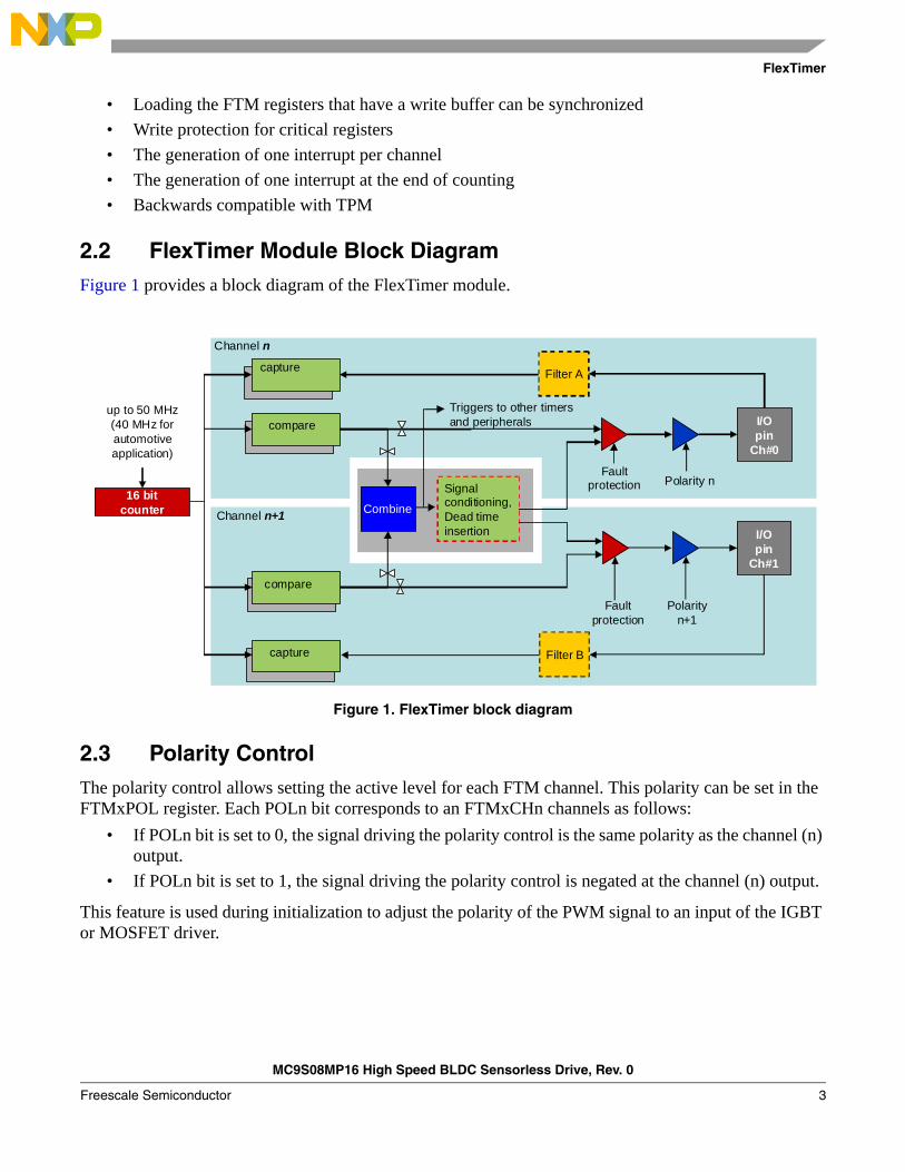
2.2 FlexTimer Module Block DiagramFigure 1 provides a block diagram of the FlexTimer module.
Figure 1. FlexTimer block diagram
2.3 Polarity ControlThe polarity control allows setting the active level for each FTM channel. This polarity can be set in the FTMxPOL register. Each POLn bit corresponds to an FTMxCHn channels as follows:
• If POLn bit is set to 0, the signal driving the polarity control is the same polarity as the channel (n) output.
• If POLn bit is set to 1, the signal driving the polarity control is negated at the channel (n) output.
This feature is used during initialization to adjust the polarity of the PWM signal to an input of the IGBT or MOSFET driver.
capture
capture
compare
Combine
I/O pin
Ch#1
Signal conditioning, Dead time insertion
Triggers to other timers and peripherals
Channel n+1
Channel n
Filter B
compare
Filter A
I/O pin
Ch#0
Fault protection
Fault protection Polarity n
Polarity n+1
16 bit counter
up to 50 MHz(40 MHz for automotiveapplication)
MC9S08MP16 High Speed BLDC Sensorless Drive, Rev. 0
Freescale Semiconductor 3
FlexTimer
NOTEAfter an MCU reset, the FTM is disabled and FTM channel pins are set to GPIO input mode. Therefore, the proper external pull-up or pull-down resistor has to be used to ensure the correct voltage level on the input of the IGBT or MOSFET driver.
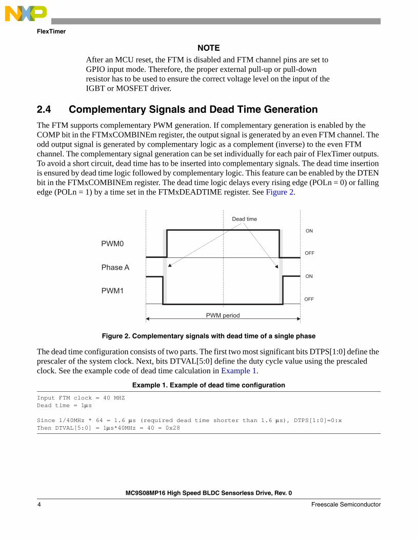
2.4 Complementary Signals and Dead Time GenerationThe FTM supports complementary PWM generation. If complementary generation is enabled by the COMP bit in the FTMxCOMBINEm register, the output signal is generated by an even FTM channel. The odd output signal is generated by complementary logic as a complement (inverse) to the even FTM channel. The complementary signal generation can be set individually for each pair of FlexTimer outputs. To avoid a short circuit, dead time has to be inserted into complementary signals. The dead time insertion is ensured by dead time logic followed by complementary logic. This feature can be enabled by the DTEN bit in the FTMxCOMBINEm register. The dead time logic delays every rising edge (POLn = 0) or falling edge (POLn = 1) by a time set in the FTMxDEADTIME register. See Figure 2.
Figure 2. Complementary signals with dead time of a single phase
The dead time configuration consists of two parts. The first two most significant bits DTPS[1:0] define the prescaler of the system clock. Next, bits DTVAL[5:0] define the duty cycle value using the prescaled clock. See the example code of dead time calculation in Example 1.
Example 1. Example of dead time configuration
Input FTM clock = 40 MHZDead time = 1s
Since 1/40MHz * 64 = 1.6 s (required dead time shorter than 1.6 s), DTPS[1:0]=0:xThen DTVAL[5:0] = 1s*40MHz = 40 = 0x28
PWM0
PWM1
Phase A
PWM period
Dead time
ON
ON
OFF
OFF
MC9S08MP16 High Speed BLDC Sensorless Drive, Rev. 0
Freescale Semiconductor4
FlexTimer
2.5 Fault ControlThe fault control logic ensures the shut down of FlexTimer outputs in the case of any fault condition. The FlexTimer is equipped with four fault pins. If the signal is active on an enabled pin, set to logic 1. The FlexTimer outputs are set to an inactive level. The inactive level is defined by polarity control (the opposite level to the active level set by polarity control). The fault control can operate in automatic fault clearing or manual fault clearing modes.
2.5.1 Enabling Fault Control
To enable fault control, the following setting has to be made:
• Set fault mode in the FTMxMODE register (FAULTM[1:0] bits). For FAULTM[1:0] bit settings see Table 1.
• Enable fault control for each pair of FTM outputs by setting the FAULTEN bit in FTMxCOMBINEm.
Table 1. Fault control mode selection
2.5.2 Automatic Fault Clearing
If automatic fault clearing is selected (FAULTM[1:0] = 11), then the disabled channel outputs are re-enabled at the beginning of each PWM pulse and the fault input signal returns to zero. This setting is usually used for implementing cycle to cycle current limitation.
2.5.3 Manual Fault Clearing
If manual fault clearing is selected (FAULTM[1:0] = 01 or 10), then disabled channel outputs are enabled when the FAULTFn bits are cleared and a new PWM cycle begins. This mode is used for fault protection. Because the fault inputs are edge sensitive only, the actual state of the fault input pins must be checked by testing the FAULTIN bit in the FTMxFMS register before clearing the FAULTFn bits.
FAULTM Fault Control Mode
00 Fault control is disabled
01 Fault control is enabled for only even channels (channels 0, 2, 4, and 6) and the manual fault clearing is selected
10 Fault control is enabled for all channels and the manual fault clearing is selected
11 Fault control is enabled for all channels and the automatic fault clearing is selected
MC9S08MP16 High Speed BLDC Sensorless Drive, Rev. 0
Freescale Semiconductor 5
FlexTimer
2.5.4 Fault Status and Interrupt Control
The fault event can generate an interrupt if enabled by the FAULTIE bit in the FTMxMODE register. The fault event is indicated by the FAULTFn bits in the FTMxFMS register. To clear the FAULTFn bit, it is necessary to do two steps:
• Read the FTMxFMS register (while the FAULTFn bit is set)
• Write 0 to FAULTFn bit, which needs to be cleared
WARNINGClearing FAULTFn bits re-enables FTM outputs on any condition because the fault inputs are only edge sensitive. Therefore, before clearing the FAULTFn bit, the actual state of the fault input pin must be checked by testing the FAULTINn bit in the FTMxFMS register.
2.5.5 Fault Input Pin Filter
Each enabled fault input signal can be filtered to avoid glitches. The filter delay is set through the FFVAL[3:0] bits in the FTMxFLTFILTER register. The filter delay is equal to 4 + FFVAL[3:0] system clocks. If the fault signal is shorter then the delay defined by the FFVAL[3:0] bits, the input signal is ignored and a fault event is not triggered. In case that the input filter is disabled, the fault signal is always delayed by two system clocks.
2.6 Enable and Disable FTM OutputsThe FTM does not directly support the function to enable and disable FTM outputs. There are two ways to enable and disable FTM:
• Using ELSnB:ELSnA bits
• Using output mask control
The ELSnB:ELSnA bits are available for each FTM channel in the FTMxCnSC registers. If ELSnB:ELSnA=00, the FTM channel output reverts to a general purpose input and output (I/O) pin. If the I/O pin is set as an input pin, the FTM outputs are forced to an inactive level by an external resistor. If the I/O pin is set as an output pin, the FTM output can be controlled through software as a standard GPIO pin. In this case, the GPIO pin has to be set to an inactive value before the ELSnB:ELSnA bits are set to zero.Another way to enable and disable FTM outputs is to use output mask control. The mask control sets the FTM channel output to an inactive level when the corresponding bit in the FTMxOUTMASK register is set. To use output mask control for this purpose, the SYNCHOM bit in the FTMxSYNC register has to be set to 0. In this case, any change in the FTMxOUTMASK register takes effect immediately. The output mask control in combination with the polarity control feature enables flexible commutation control in the BLDC motor control applications.
2.7 Channel Duty Cycle Update SynchronizationTo generate consistent PWM signals on multiple FTM channels, the update of duty cycles for all channels has to be synchronized, specifically when the duty cycle update is done asynchronously. The channel duty cycle update synchronization is available in the FTMxSYNC register. Before synchronization is used, it
MC9S08MP16 High Speed BLDC Sensorless Drive, Rev. 0
Freescale Semiconductor6
FlexTimer
has to be enabled individually for each pair of FTM outputs by setting the SYNCEN bit to 1 in the FTMxCOMBINEm register.
The duty cycle update synchronization is controlled by CNTMAX and CNTMIN. These bits define where the duty cycle update takes place. If CNTMAX is set to 1, the duty cycle update is finished when the FTM counter reaches its maximal value. If CNTMIN is set to 1, the duty cycle update is finished when the FTM counter reaches its minimal value.
The four most significant bits (SWSYNC, and TRIG2-0) trigger the duty cycle update. The SWSYNC bit allows triggering a duty cycle update through software. The next three bits (TRIG2-0) allow triggering a duty cycle update through an external event. The source signal for the TRIG2-0 bits can be found in the datasheet titled MC9S08MP16 Series Data Sheet (document MC9S08MP16DS) for the MC9S08MP16 microcontroller.
When the SWSYNC bit is set to 1, the duty cycle update occurs on the next event corresponding to the CNTMAX and CNTMIN settings after the SWSYNC bit is set. If CNTMAX is set to 1, the duty cycle update occurs when the FTM counter reaches the maximal value after the SWSYNC bit is set. Similarly, if CNTMIN is set to 1 the duty cycle update occurs when FTM counter reaches its minimal value after the SWSYNC bit is set. The SWSYNC bit is cleared automatically after the duty cycle update. The SWSYNC bit corresponds to the LDOK bit on other PWM modules used by Freescale microcontrollers.
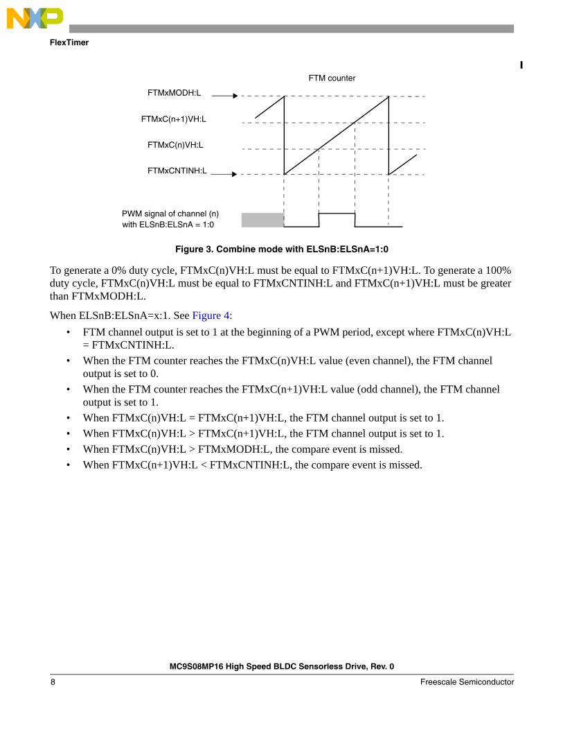
2.8 Combine PWM ModeThe FTM offers a completely new way of generating PWM signals, this is a combine mode. The combine mode merges two FTM channels to generate a single PWM signal. This mode allows controlling both edges of a PWM signal individually. The even channel controls the first edge, the odd channel controls the second edge in the PWM period. The combine mode is enabled by setting the COMBINE bit to 1 in the FTMxCOMBINEm register. The period of the PWM signal is defined by FTMxMODH:L and FTMxCNTINH:L. The FTMxCNTINH:L value can even be a negative value as shown later (see Section 2.8.2, “Generation of Center-Aligned PWM in Combine Mode”). To ensure correct PWM generation, the FTMxMODH:L value must be greater than FTMxCNTINH:L. The PWM duty cycle is defined by the FTMxC(n)VH:L and FTMxC(n+1)VH:L registers in the following way:
When ELSnB:ELSnA=1:0. See Figure 3:
• FTM channel output is cleared (set to 0) at the beginning of a PWM period, except where FTMxC(n)VH:L = FTMxCNTINH:L.
• When the FTM counter reaches the FTMxC(n)VH:L value (even channel), the FTM channel output is set to 1.
• When the FTM counter reaches the FTMxC(n+1)VH:L value (odd channel), the FTM channel output is set to 0.
• When FTMxC(n)VH:L = FTMxC(n+1)VH:L, the FTM channel output is set to 0.
• When FTMxC(n)VH:L > FTMxC(n+1)VH:L, the FTM channel output is set to 0.
• When FTMxC(n)VH:L > FTMxMODH:L, the compare event is missed.
• When FTMxC(n+1)VH:L < FTMxCNTINH:L, the compare event is missed.
MC9S08MP16 High Speed BLDC Sensorless Drive, Rev. 0
Freescale Semiconductor 7
FlexTimer
Figure 3. Combine mode with ELSnB:ELSnA=1:0
To generate a 0% duty cycle, FTMxC(n)VH:L must be equal to FTMxC(n+1)VH:L. To generate a 100% duty cycle, FTMxC(n)VH:L must be equal to FTMxCNTINH:L and FTMxC(n+1)VH:L must be greater than FTMxMODH:L.
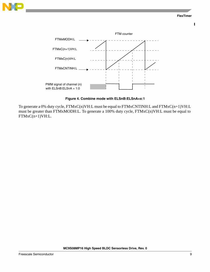
When ELSnB:ELSnA=x:1. See Figure 4:
• FTM channel output is set to 1 at the beginning of a PWM period, except where FTMxC(n)VH:L = FTMxCNTINH:L.
• When the FTM counter reaches the FTMxC(n)VH:L value (even channel), the FTM channel output is set to 0.
• When the FTM counter reaches the FTMxC(n+1)VH:L value (odd channel), the FTM channel output is set to 1.
• When FTMxC(n)VH:L = FTMxC(n+1)VH:L, the FTM channel output is set to 1.
• When FTMxC(n)VH:L > FTMxC(n+1)VH:L, the FTM channel output is set to 1.
• When FTMxC(n)VH:L > FTMxMODH:L, the compare event is missed.
• When FTMxC(n+1)VH:L < FTMxCNTINH:L, the compare event is missed.
FTM counter
FTMxMODH:L
FTMxCNTINH:L
FTMxC(n)VH:L
FTMxC(n+1)VH:L
PWM signal of channel (n)with ELSnB:ELSnA = 1:0
MC9S08MP16 High Speed BLDC Sensorless Drive, Rev. 0
Freescale Semiconductor8
FlexTimer
Figure 4. Combine mode with ELSnB:ELSnA=x:1
To generate a 0% duty cycle, FTMxC(n)VH:L must be equal to FTMxCNTINH:L and FTMxC(n+1)VH:L must be greater than FTMxMODH:L. To generate a 100% duty cycle, FTMxC(n)VH:L must be equal to FTMxC(n+1)VH:L.
FTM counter
FTMxMODH:L
FTMxCNTINH:L
FTMxC(n)VH:L
FTMxC(n+1)VH:L
PWM signal of channel (n)with ELSnB:ELSnA = 1:0
MC9S08MP16 High Speed BLDC Sensorless Drive, Rev. 0
Freescale Semiconductor 9
FlexTimer
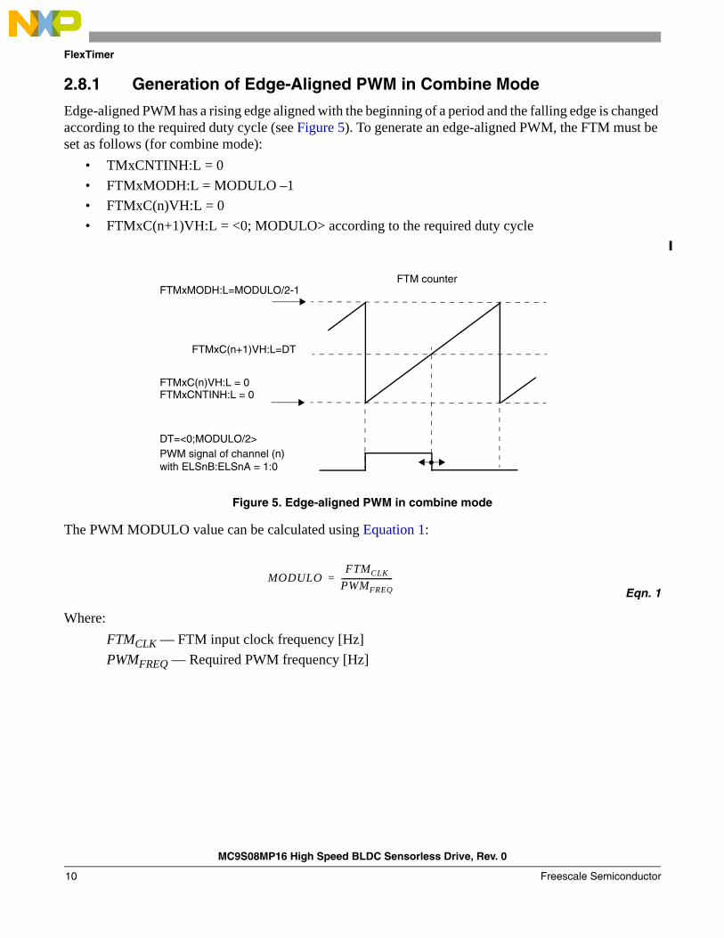
2.8.1 Generation of Edge-Aligned PWM in Combine Mode
Edge-aligned PWM has a rising edge aligned with the beginning of a period and the falling edge is changed according to the required duty cycle (see Figure 5). To generate an edge-aligned PWM, the FTM must be set as follows (for combine mode):
• TMxCNTINH:L = 0
• FTMxMODH:L = MODULO –1
• FTMxC(n)VH:L = 0
• FTMxC(n+1)VH:L = <0; MODULO> according to the required duty cycle
Figure 5. Edge-aligned PWM in combine mode
The PWM MODULO value can be calculated using Equation 1:
Eqn. 1
Where:
FTMCLK — FTM input clock frequency [Hz]
PWMFREQ — Required PWM frequency [Hz]
FTM counter
FTMxCNTINH:L = 0FTMxC(n)VH:L = 0
PWM signal of channel (n)with ELSnB:ELSnA = 1:0
FTMxMODH:L=MODULO/2-1
FTMxC(n+1)VH:L=DT
DT=<0;MODULO/2>
MODULOFTMCLK
PWMFREQ--------------------------=
MC9S08MP16 High Speed BLDC Sensorless Drive, Rev. 0
Freescale Semiconductor10
FlexTimer
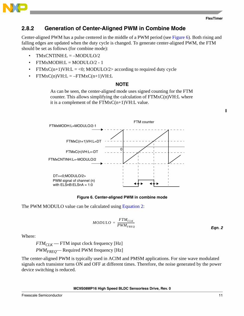
2.8.2 Generation of Center-Aligned PWM in Combine Mode
Center-aligned PWM has a pulse centered in the middle of a PWM period (see Figure 6). Both rising and falling edges are updated when the duty cycle is changed. To generate center-aligned PWM, the FTM should be set as follows (for combine mode):
• TMxCNTINH:L = –MODULO/2
• FTMxMODH:L = MODULO/2 - 1
• FTMxC(n+1)VH:L = <0; MODULO/2> according to required duty cycle
• FTMxC(n)VH:L = –FTMxC(n+1)VH:L
NOTEAs can be seen, the center-aligned mode uses signed counting for the FTM counter. This allows simplifying the calculation of FTMxC(n)VH:L where it is a complement of the FTMxC(n+1)VH:L value.
Figure 6. Center-aligned PWM in combine mode
The PWM MODULO value can be calculated using Equation 2:
Eqn. 2
Where:
FTMCLK — FTM input clock frequency [Hz]
PWMFREQ— Required PWM frequency [Hz]
The center-aligned PWM is typically used in ACIM and PMSM applications. For sine wave modulated signals each transistor turns ON and OFF at different times. Therefore, the noise generated by the power device switching is reduced.
FTM counterFTMxMODH:L=MODULO/2-1
FTMxCNTINH:L=-MODULO/2
FTMxC(n)VH:L=-DT
FTMxC(n+1)VH:L=DT
PWM signal of channel (n)with ELSnB:ELSnA = 1:0
0
DT=<0;MODULO/2>
MODULOFTMCLK
PWMFREQ--------------------------=
MC9S08MP16 High Speed BLDC Sensorless Drive, Rev. 0
Freescale Semiconductor 11
ADC Module
3 ADC Module
3.1 ADC FeaturesThe ADC module features include:
• Linear successive approximation algorithm with 12-bit resolution
• Output formatted in 12-bit, 10-bit, or 8-bit right-justified unsigned format
• Single or continuous conversion, automatic return to idle after a single conversion
• Configurable sample time and conversion speed and power
• Conversion complete flag and interrupt
• Input clock selectable up to four sources
• Asynchronous clock source for lower noise operation
• Selectable asynchronous hardware conversion trigger
• Automatic compare with interrupt for less-than, greater-than, or equal-to a programmable value
• Temperature sensor
3.2 Channel Assignments
The ADC module on MC9S08MP16 devices enables the following input signal measurements:
• 13 analogue input pins
• Programmable Gain Amplifier (PGA) output—Can be used for low amplitude signals (that is, currents)
• Internal temperature sensor. For more information on using the temperature sensor, see the application note titled Temperature Sensor for the HCS08 Microcontroller Family (document AN3031)
• Internal bandgap voltage
• High reference voltage—Internally tied to analogue power supply
• Low reference voltage—Internally tied to analogue ground
MC9S08MP16 High Speed BLDC Sensorless Drive, Rev. 0
Freescale Semiconductor12
ADC Module
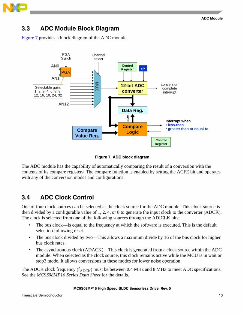
3.3 ADC Module Block DiagramFigure 7 provides a block diagram of the ADC module.
Figure 7. ADC block diagram
The ADC module has the capability of automatically comparing the result of a conversion with the contents of its compare registers. The compare function is enabled by setting the ACFE bit and operates with any of the conversion modes and configurations.
3.4 ADC Clock ControlOne of four clock sources can be selected as the clock source for the ADC module. This clock source is then divided by a configurable value of 1, 2, 4, or 8 to generate the input clock to the converter (ADCK). The clock is selected from one of the following sources through the ADICLK bits:
• The bus clock—Is equal to the frequency at which the software is executed. This is the default selection following reset.
• The bus clock divided by two—This allows a maximum divide by 16 of the bus clock for higher bus clock rates.
• The asynchronous clock (ADACK)—This clock is generated from a clock source within the ADC module. When selected as the clock source, this clock remains active while the MCU is in wait or stop3 mode. It allows conversions in these modes for lower noise operation.
The ADCK clock frequency (fADCK) must be between 0.4 MHz and 8 MHz to meet ADC specifications. See the MC9S08MP16 Series Data Sheet for the details.
12-bit ADC converter
Data Reg.
AN0
AN12
MU
X
PGA
AN1
PGASynch
Channelselect
conversioncompleteinterrupt
Compare Value Reg.
CompareLogic
SU
M
ControlRegister clk
ControlRegister
Interrupt when• less-than• greater than or equal-to
Selectable gain:1, 2, 3, 4, 6, 8, 9,12, 16, 18, 24, 32
MC9S08MP16 High Speed BLDC Sensorless Drive, Rev. 0
Freescale Semiconductor 13
ADC Module
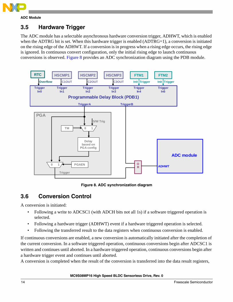
3.5 Hardware TriggerThe ADC module has a selectable asynchronous hardware conversion trigger, ADHWT, which is enabled when the ADTRG bit is set. When this hardware trigger is enabled (ADTRG=1), a conversion is initiated on the rising edge of the ADHWT. If a conversion is in progress when a rising edge occurs, the rising edge is ignored. In continuous convert configuration, only the initial rising edge to launch continuous conversions is observed. Figure 8 provides an ADC synchronization diagram using the PDB module.
Figure 8. ADC synchronization diagram
3.6 Conversion ControlA conversion is initiated:
• Following a write to ADCSC1 (with ADCH bits not all 1s) if a software triggered operation is selected.
• Following a hardware trigger (ADHWT) event if a hardware triggered operation is selected.
• Following the transferred result to the data registers when continuous conversion is enabled.
If continuous conversions are enabled, a new conversion is automatically initiated after the completion of the current conversion. In a software triggered operation, continuous conversions begin after ADCSC1 is written and continues until aborted. In a hardware triggered operation, continuous conversions begin after a hardware trigger event and continues until aborted.A conversion is completed when the result of the conversion is transferred into the data result registers,
0 1
RTC HSCMP1 HSCMP2 HSCMP3 FTM1 FTM2
Overflow C1OUT C2OUT C3OUT Init Trigger Init Trigger
Programmable Delay Block (PDB1)
TriggerIn0
TriggerIn1
TriggerIn2
TriggerIn3
TriggerIn4
TriggerIn5
TriggerA TriggerB
S/W Trig
TM
Delaybased on
PGA config
0 1 PGAEN
PGA
Trigger
OR
ADC module
ADHWT
MC9S08MP16 High Speed BLDC Sensorless Drive, Rev. 0
Freescale Semiconductor14
Programmable Delay Block (PDB)
ADCRH and ADCRL. This is indicated by the setting of COCO. An interrupt is generated if AIEN is high at the time that COCO is set.
4 Programmable Delay Block (PDB)The purpose of this block is to:
• Manages the delay between an external event and the time the comparator, ADC, or PGA samples are taken.
• Generate PWM pulses that are synchronized to the FlexTimer, comparators output, or RTC.
The trigger signal can be selected for the FlexTimer’s initial trigger, comparators output, RTC overflow, or software starts the PBD, or resets the PBD counter if the PDB is in continuous mode. A single one-shot pulse or pulse string can be generated in reply to a response trigger.
4.1 Features• 16-bit resolution with prescaler
• Positive transition of trigger event signal initiates the counter
• Supports two triggered delay outputs. Each has an independently-controlled delay from the trigger event
• PDB outputs can be ORed together to schedule two conversions from one input trigger event
• PDB outputs can schedule precise edge placement for a pulsed output. This feature is used to generate the control signal for the HSCMP windowing feature and output to a package pin if needed for applications, such as a critical conductive mode power factor correction.
• Continuous-pulse output or single-shot mode supported
MC9S08MP16 High Speed BLDC Sensorless Drive, Rev. 0
Freescale Semiconductor 15
Programmable Delay Block (PDB)
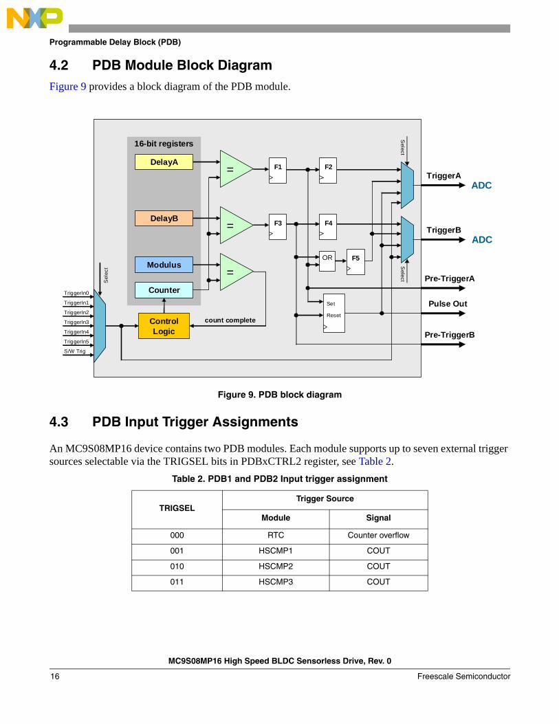
4.2 PDB Module Block DiagramFigure 9 provides a block diagram of the PDB module.
Figure 9. PDB block diagram
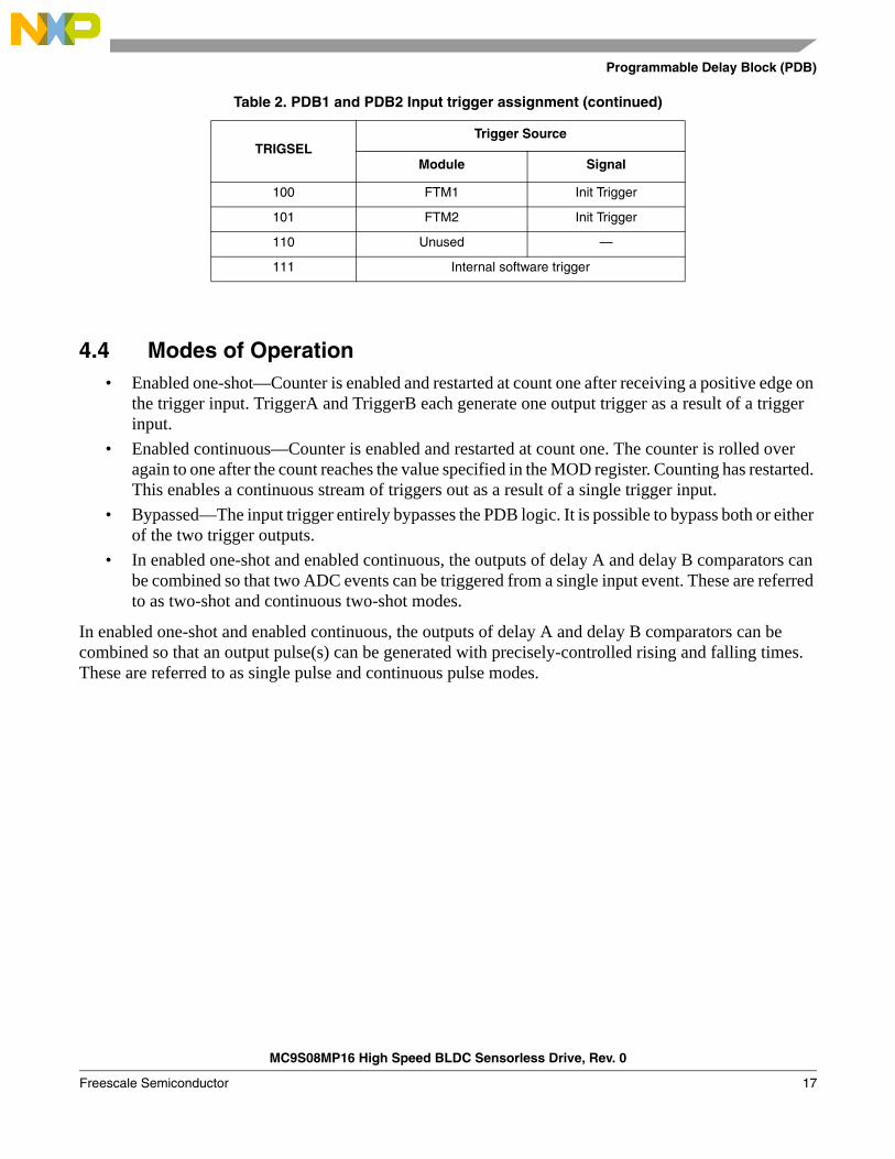
4.3 PDB Input Trigger Assignments
An MC9S08MP16 device contains two PDB modules. Each module supports up to seven external trigger sources selectable via the TRIGSEL bits in PDBxCTRL2 register, see Table 2.
Table 2. PDB1 and PDB2 Input trigger assignment
TRIGSELTrigger Source
Module Signal
000 RTC Counter overflow
001 HSCMP1 COUT
010 HSCMP2 COUT
011 HSCMP3 COUT
DelayA
DelayB
=
=
=Modulus
Counter
16-bit registers
ControlLogic
count complete
TriggerA
TriggerB
OR
F1
F3
F2
F4
F5
Pre-TriggerA
Set
Reset
Pre-TriggerB
Pulse Out
TriggerIn0
TriggerIn1
TriggerIn2
TriggerIn3
TriggerIn4
TriggerIn5
S/W Trig
Sel
ect
Select
Select
ADC
ADC
MC9S08MP16 High Speed BLDC Sensorless Drive, Rev. 0
Freescale Semiconductor16
Programmable Delay Block (PDB)
4.4 Modes of Operation• Enabled one-shot—Counter is enabled and restarted at count one after receiving a positive edge on
the trigger input. TriggerA and TriggerB each generate one output trigger as a result of a trigger input.
• Enabled continuous—Counter is enabled and restarted at count one. The counter is rolled over again to one after the count reaches the value specified in the MOD register. Counting has restarted. This enables a continuous stream of triggers out as a result of a single trigger input.
• Bypassed—The input trigger entirely bypasses the PDB logic. It is possible to bypass both or either of the two trigger outputs.
• In enabled one-shot and enabled continuous, the outputs of delay A and delay B comparators can be combined so that two ADC events can be triggered from a single input event. These are referred to as two-shot and continuous two-shot modes.
In enabled one-shot and enabled continuous, the outputs of delay A and delay B comparators can be combined so that an output pulse(s) can be generated with precisely-controlled rising and falling times. These are referred to as single pulse and continuous pulse modes.
100 FTM1 Init Trigger
101 FTM2 Init Trigger
110 Unused —
111 Internal software trigger
Table 2. PDB1 and PDB2 Input trigger assignment (continued)
TRIGSELTrigger Source
Module Signal
MC9S08MP16 High Speed BLDC Sensorless Drive, Rev. 0
Freescale Semiconductor 17
Example of Using the MC9S08MP16 in a High Speed BLDC Sensorless Application
5 Example of Using the MC9S08MP16 in a High Speed BLDC Sensorless Application
This chapter describes an example of using the FTM, PDB, and ADC modules in a high speed BLDC sensorless application, configuration examples, the timing, and hardware interconnections of modules inside the controller.
5.1 PWM Generation Using the FlexTimer Module
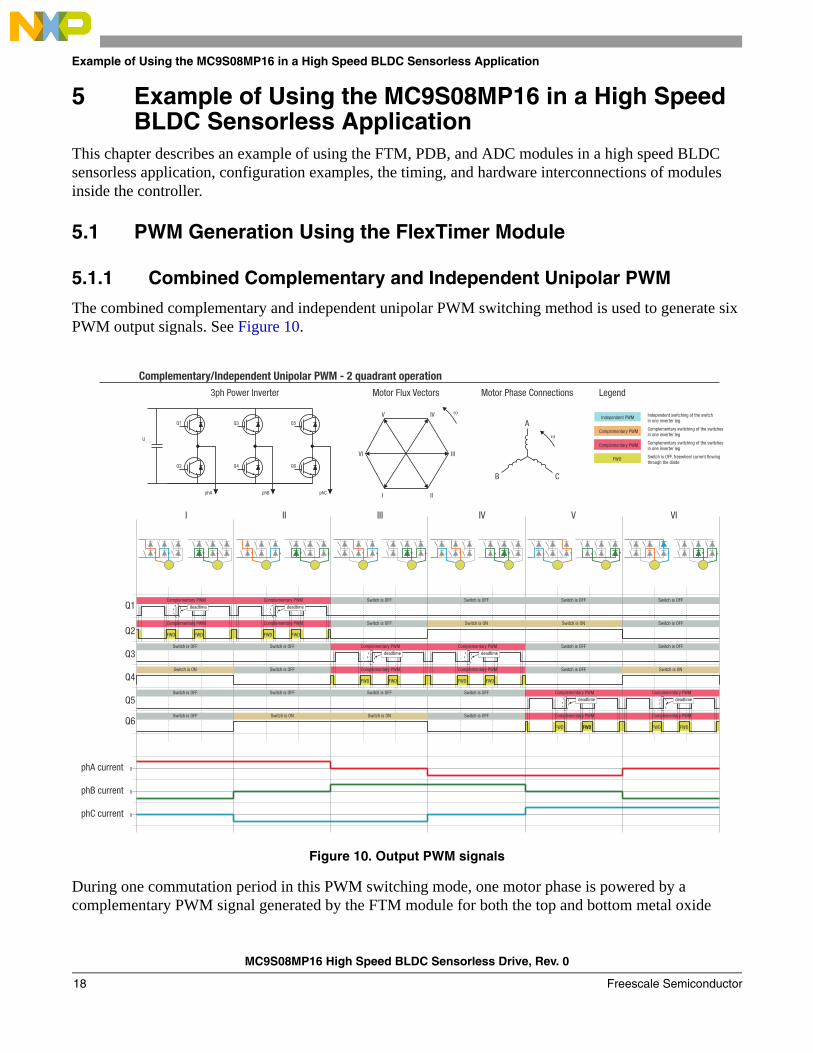
5.1.1 Combined Complementary and Independent Unipolar PWM
The combined complementary and independent unipolar PWM switching method is used to generate six PWM output signals. See Figure 10.
Figure 10. Output PWM signals
During one commutation period in this PWM switching mode, one motor phase is powered by a complementary PWM signal generated by the FTM module for both the top and bottom metal oxide
MC9S08MP16 High Speed BLDC Sensorless Drive, Rev. 0
Freescale Semiconductor18
Example of Using the MC9S08MP16 in a High Speed BLDC Sensorless Application
semiconductor field effect transistors (MOSFET) while the second motor phase is grounded by the bottom MOSFET transistor which is on all the time during the commutation period. Within this commutation period, the third motor phase is unpowered and is used for the back electromagnetic force (back-EMF) signal measurement by the ADC for zero-cross detection.
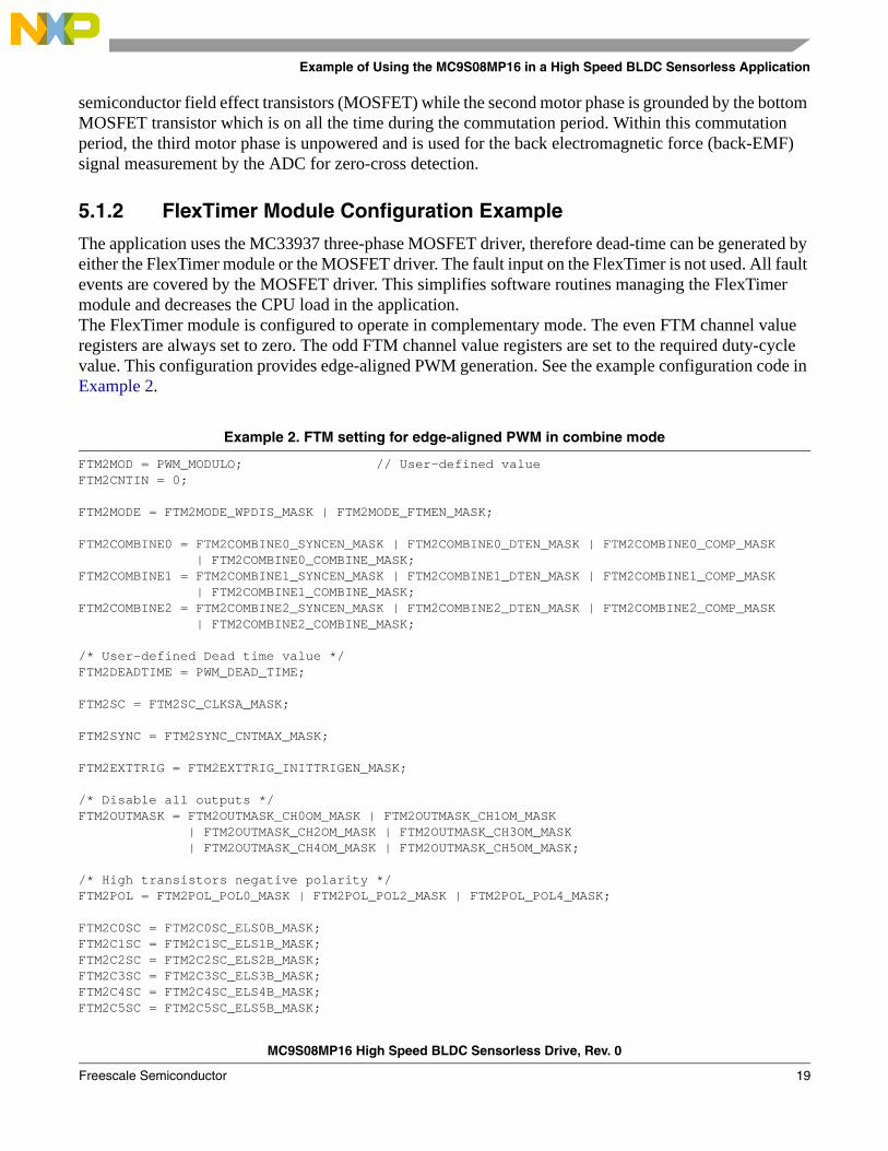
5.1.2 FlexTimer Module Configuration Example
The application uses the MC33937 three-phase MOSFET driver, therefore dead-time can be generated by either the FlexTimer module or the MOSFET driver. The fault input on the FlexTimer is not used. All fault events are covered by the MOSFET driver. This simplifies software routines managing the FlexTimer module and decreases the CPU load in the application.The FlexTimer module is configured to operate in complementary mode. The even FTM channel value registers are always set to zero. The odd FTM channel value registers are set to the required duty-cycle value. This configuration provides edge-aligned PWM generation. See the example configuration code in Example 2.
Example 2. FTM setting for edge-aligned PWM in combine mode
FTM2MOD = PWM_MODULO; // User-defined valueFTM2CNTIN = 0;
FTM2MODE = FTM2MODE_WPDIS_MASK | FTM2MODE_FTMEN_MASK;
FTM2COMBINE0 = FTM2COMBINE0_SYNCEN_MASK | FTM2COMBINE0_DTEN_MASK | FTM2COMBINE0_COMP_MASK| FTM2COMBINE0_COMBINE_MASK;
FTM2COMBINE1 = FTM2COMBINE1_SYNCEN_MASK | FTM2COMBINE1_DTEN_MASK | FTM2COMBINE1_COMP_MASK| FTM2COMBINE1_COMBINE_MASK;
FTM2COMBINE2 = FTM2COMBINE2_SYNCEN_MASK | FTM2COMBINE2_DTEN_MASK | FTM2COMBINE2_COMP_MASK | FTM2COMBINE2_COMBINE_MASK;
/* User-defined Dead time value */FTM2DEADTIME = PWM_DEAD_TIME; FTM2SC = FTM2SC_CLKSA_MASK;
FTM2SYNC = FTM2SYNC_CNTMAX_MASK;
FTM2EXTTRIG = FTM2EXTTRIG_INITTRIGEN_MASK;
/* Disable all outputs */FTM2OUTMASK = FTM2OUTMASK_CH0OM_MASK | FTM2OUTMASK_CH1OM_MASK
| FTM2OUTMASK_CH2OM_MASK | FTM2OUTMASK_CH3OM_MASK| FTM2OUTMASK_CH4OM_MASK | FTM2OUTMASK_CH5OM_MASK;
/* High transistors negative polarity */FTM2POL = FTM2POL_POL0_MASK | FTM2POL_POL2_MASK | FTM2POL_POL4_MASK; FTM2C0SC = FTM2C0SC_ELS0B_MASK;FTM2C1SC = FTM2C1SC_ELS1B_MASK;FTM2C2SC = FTM2C2SC_ELS2B_MASK;FTM2C3SC = FTM2C3SC_ELS3B_MASK;FTM2C4SC = FTM2C4SC_ELS4B_MASK;FTM2C5SC = FTM2C5SC_ELS5B_MASK;
MC9S08MP16 High Speed BLDC Sensorless Drive, Rev. 0
Freescale Semiconductor 19
Example of Using the MC9S08MP16 in a High Speed BLDC Sensorless Application
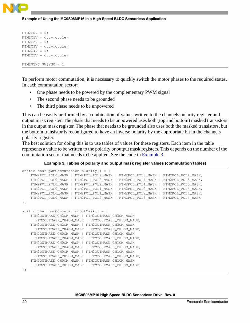
FTM2C0V = 0;FTM2C1V = duty_cycle;FTM2C2V = 0;FTM2C3V = duty_cycle;FTM2C4V = 0;FTM2C5V = duty_cycle;
FTM2SYNC_SWSYNC = 1;
To perform motor commutation, it is necessary to quickly switch the motor phases to the required states. In each commutation sector:
• One phase needs to be powered by the complementary PWM signal
• The second phase needs to be grounded
• The third phase needs to be unpowered
This can be easily performed by a combination of values written to the channels polarity register and output mask register. The phase that needs to be unpowered uses both (top and bottom) masked transistors in the output mask register. The phase that needs to be grounded also uses both the masked transistors, but the bottom transistor is reconfigured to have an inverse polarity by the appropriate bit in the channels polarity register.The best solution for doing this is to use tables of values for these registers. Each item in the table represents a value to be written to the polarity or output mask registers. This depends on the number of the commutation sector that needs to be applied. See the code in Example 3.
Example 3. Tables of polarity and output mask register values (commutation tables)
static char pwmCommutationPolarity[] = { FTM2POL_POL0_MASK | FTM2POL_POL2_MASK | FTM2POL_POL3_MASK | FTM2POL_POL4_MASK, FTM2POL_POL0_MASK | FTM2POL_POL2_MASK | FTM2POL_POL4_MASK | FTM2POL_POL5_MASK, FTM2POL_POL0_MASK | FTM2POL_POL2_MASK | FTM2POL_POL4_MASK | FTM2POL_POL5_MASK, FTM2POL_POL0_MASK | FTM2POL_POL1_MASK | FTM2POL_POL2_MASK | FTM2POL_POL4_MASK, FTM2POL_POL0_MASK | FTM2POL_POL1_MASK | FTM2POL_POL2_MASK | FTM2POL_POL4_MASK, FTM2POL_POL0_MASK | FTM2POL_POL2_MASK | FTM2POL_POL3_MASK | FTM2POL_POL4_MASK };
static char pwmCommutationOutMask[] = {FTM2OUTMASK_CH2OM_MASK | FTM2OUTMASK_CH3OM_MASK| FTM2OUTMASK_CH4OM_MASK | FTM2OUTMASK_CH5OM_MASK,
FTM2OUTMASK_CH2OM_MASK | FTM2OUTMASK_CH3OM_MASK| FTM2OUTMASK_CH4OM_MASK | FTM2OUTMASK_CH5OM_MASK,
FTM2OUTMASK_CH0OM_MASK | FTM2OUTMASK_CH1OM_MASK| FTM2OUTMASK_CH4OM_MASK | FTM2OUTMASK_CH5OM_MASK,
FTM2OUTMASK_CH0OM_MASK | FTM2OUTMASK_CH1OM_MASK| FTM2OUTMASK_CH4OM_MASK | FTM2OUTMASK_CH5OM_MASK,
FTM2OUTMASK_CH0OM_MASK | FTM2OUTMASK_CH1OM_MASK| FTM2OUTMASK_CH2OM_MASK | FTM2OUTMASK_CH3OM_MASK,
FTM2OUTMASK_CH0OM_MASK | FTM2OUTMASK_CH1OM_MASK| FTM2OUTMASK_CH2OM_MASK | FTM2OUTMASK_CH3OM_MASK
};
MC9S08MP16 High Speed BLDC Sensorless Drive, Rev. 0
Freescale Semiconductor20
Example of Using the MC9S08MP16 in a High Speed BLDC Sensorless Application
Using these configuration tables highly simplifies the commutation routine. The update of the FTM channel value registers is not dependent on the actual commutation sector. See the code in Example 4.
Example 4. Commutation code and duty-cycle update code
/* Commutation codepwmSector - number of the actual commutation sector in range 0 to 5 */
FTM2POL = pwmCommutationPolarity[pwmSector];FTM2OUTMASK = pwmCommutationOutMask[pwmSector];/* apply new PWM Output Mask Register configuration */FTM2SYNC_SWSYNC = 1;
...
...
.../* Duty-cycle update code*//* Apply new PWM duty cycles */ /* Phase A */FTM2C1V = duty_cycle;/* Phase B */FTM2C3V = duty_cycle;/* Phase C */FTM2C5V = duty_cycle;/* apply new PWM duty-cycle values */FTM2SYNC_SWSYNC = 1;
5.2 Back-EMF ProcessingFor the sensorless BLDC application, it is necessary to sense the following parameters during the application run:
• DC bus voltage
• DC bus current for current and torque limiting
• Phase A, B, and C back-EMF voltages
The commutation time and period are calculated from these measured parameters. The hardware abilities of the peripheral modules on the S08MP16 controller significantly reduce the CPU load on the user software and enables precise sensorless BLDC motor control.
5.2.1 Back-EMF Voltage Sensing
The back-EMF voltage sensing is needed for sensorless motor control. In applications with a BLDC motor only two phases are powered at a time during each commutation period. The third phase is always unpowered. Because the motor shaft is rotating and there are permanent magnets on the rotor producing the magnetic field there is a back-EMF voltage generated on the phase coils during the rotor motion. This voltage can be measured in the currently unpowered phase by the ADC module. The actual rotor position can be evaluated from this information. Back-EMF voltage can be positive or negative depending on the actual rotor position, therefore it is necessary to measure this voltage when the other two motor phases are powered. This means that when one phase is grounded and the second is connected to the DC bus positive voltage line. The measured back-EMF voltage can then be evaluated as:
MC9S08MP16 High Speed BLDC Sensorless Drive, Rev. 0
Freescale Semiconductor 21
Example of Using the MC9S08MP16 in a High Speed BLDC Sensorless Application
• Positive when Back-EMF voltage > DC Bus voltage / 2
• Negative when Back-EMF voltage < DC bus voltage / 2
NOTEIt is important to know that if the back-EMF voltage generated by the motor is zero — the measured back-EMF voltage is equal to DC bus voltage / 2 during the active PWM pulse on the output—then the motor shaft is just in the middle of two commutations. A principle of the sensorless motor control application is simply to find the back-EMF voltage zero-cross, and from the two last zero-cross events the time of next commutation can be easily calculated.
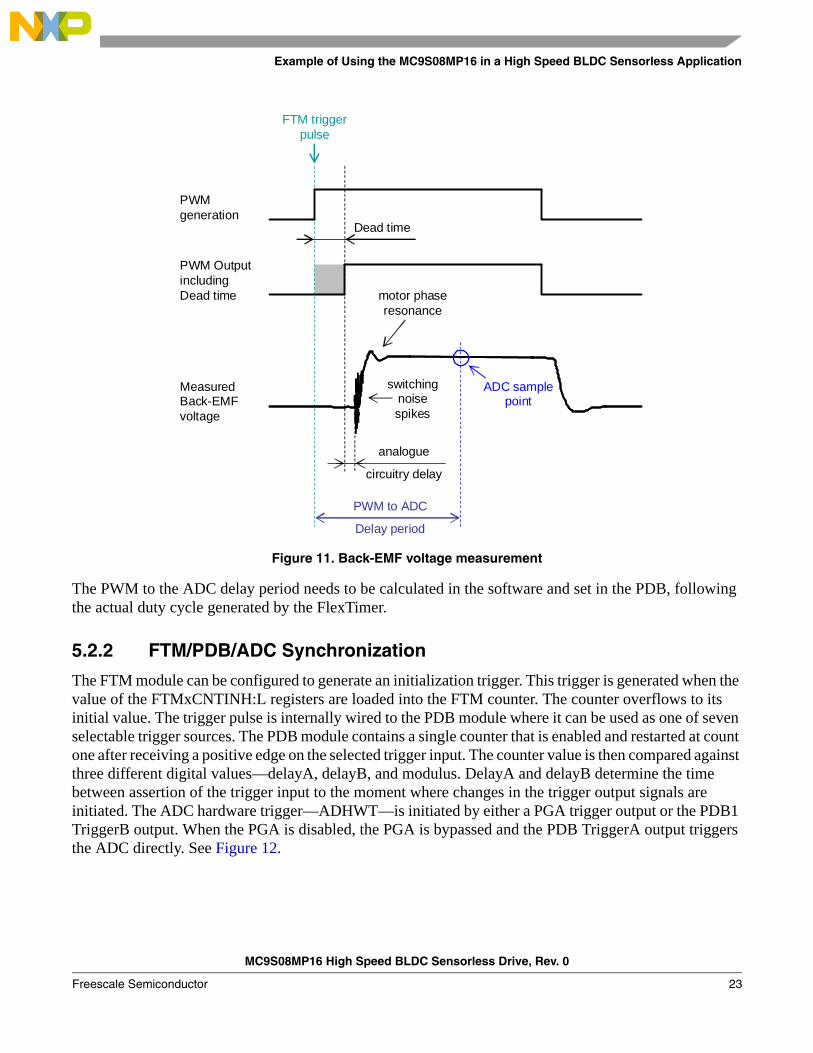
The ADC sample point needs to be set for back-EMF sensing. An ADC sample point depends on parameters of the application; dead time used in PWM, analogue circuitry delay, power components switching noise, motor coil transient actions due to PWM switching, and motor parameters. The ADC sample point can be precisely synchronized from the PWM module (FTM) using the PDB module. The PDB module can be configured to use hardware triggers from the FTM module as an input to start counting and can generate a hardware trigger as output to the ADC module when the internal PDB counter reaches a configured delay (see Figure 11). Back-EMF voltage is measured once every PWM period, that is once every 50 s, if a 20 kHz output PWM frequency is used.
MC9S08MP16 High Speed BLDC Sensorless Drive, Rev. 0
Freescale Semiconductor22
Example of Using the MC9S08MP16 in a High Speed BLDC Sensorless Application
Figure 11. Back-EMF voltage measurement
The PWM to the ADC delay period needs to be calculated in the software and set in the PDB, following the actual duty cycle generated by the FlexTimer.
5.2.2 FTM/PDB/ADC Synchronization
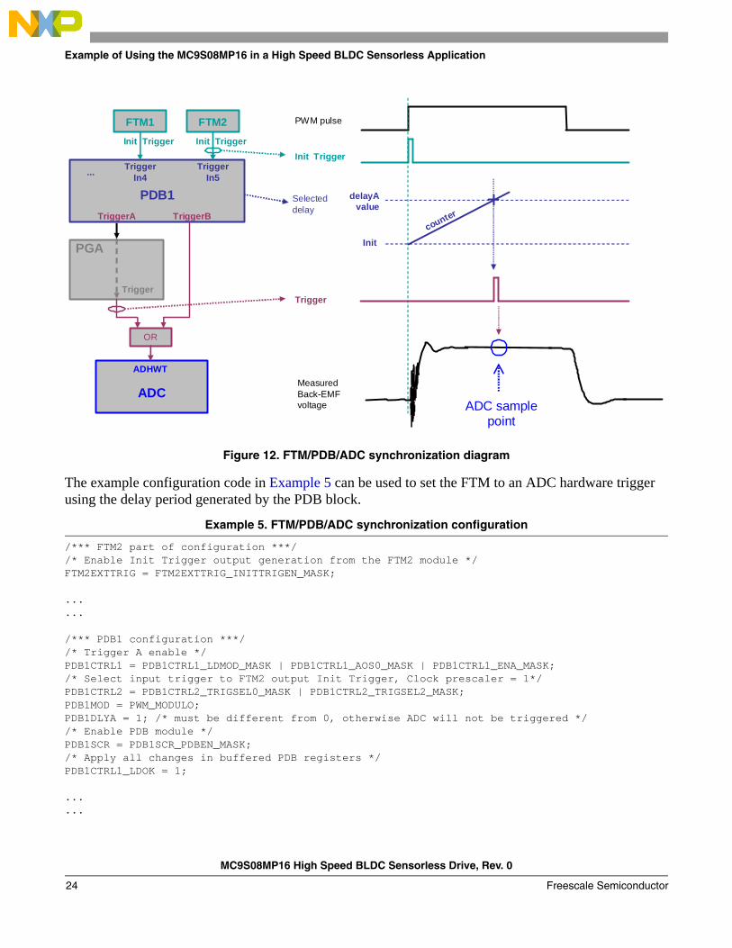
The FTM module can be configured to generate an initialization trigger. This trigger is generated when the value of the FTMxCNTINH:L registers are loaded into the FTM counter. The counter overflows to its initial value. The trigger pulse is internally wired to the PDB module where it can be used as one of seven selectable trigger sources. The PDB module contains a single counter that is enabled and restarted at count one after receiving a positive edge on the selected trigger input. The counter value is then compared against three different digital values—delayA, delayB, and modulus. DelayA and delayB determine the time between assertion of the trigger input to the moment where changes in the trigger output signals are initiated. The ADC hardware trigger—ADHWT—is initiated by either a PGA trigger output or the PDB1 TriggerB output. When the PGA is disabled, the PGA is bypassed and the PDB TriggerA output triggers the ADC directly. See Figure 12.
Dead time
PWM Outputincluding Dead time
PWM generation
MeasuredBack-EMFvoltage
switchingnoise spikes
motor phaseresonance
ADC samplepoint
FTM triggerpulse
PWM to ADC
Delay period
analogue
circuitry delay
MC9S08MP16 High Speed BLDC Sensorless Drive, Rev. 0
Freescale Semiconductor 23
Example of Using the MC9S08MP16 in a High Speed BLDC Sensorless Application
Figure 12. FTM/PDB/ADC synchronization diagram
The example configuration code in Example 5 can be used to set the FTM to an ADC hardware trigger using the delay period generated by the PDB block.
Example 5. FTM/PDB/ADC synchronization configuration
/*** FTM2 part of configuration ***//* Enable Init Trigger output generation from the FTM2 module */FTM2EXTTRIG = FTM2EXTTRIG_INITTRIGEN_MASK;
...
...
/*** PDB1 configuration ***//* Trigger A enable */PDB1CTRL1 = PDB1CTRL1_LDMOD_MASK | PDB1CTRL1_AOS0_MASK | PDB1CTRL1_ENA_MASK;/* Select input trigger to FTM2 output Init Trigger, Clock prescaler = 1*/PDB1CTRL2 = PDB1CTRL2_TRIGSEL0_MASK | PDB1CTRL2_TRIGSEL2_MASK;PDB1MOD = PWM_MODULO;PDB1DLYA = 1; /* must be different from 0, otherwise ADC will not be triggered *//* Enable PDB module */PDB1SCR = PDB1SCR_PDBEN_MASK;/* Apply all changes in buffered PDB registers */PDB1CTRL1_LDOK = 1;
...
...
FTM1 FTM2
Init Trigger Init Trigger
PDB1
TriggerIn4
TriggerIn5
TriggerA TriggerB
PGA
Trigger
OR
ADC
ADHWT
...
PWM pulse
Init Trigger
ADC samplepoint
MeasuredBack-EMFvoltage
delayAvalue
Init
Trigger
Selecteddelay
counter
MC9S08MP16 High Speed BLDC Sensorless Drive, Rev. 0
Freescale Semiconductor24
Example of Using the MC9S08MP16 in a High Speed BLDC Sensorless Application
/*** ADC part of configuration ***//* Enable ADC H/W triggering */ADCSC2 = ADCSC2_ADTRG_MASK;
...
...
/* Set new delay value to the middle of the PWM pulse* duty_cycle - value used in FlexTimer to set duty-cycle. Because FTM operates at twice clock* frequency as PDB, and we need to trigger ADC in the middle of the PWM pulse, it’s needed to* shift duty_cycle twice to the right* ADC2PWM_DELAY_OFFSET - Additional delay related to Analogue circuitry, dead-time, etc. */PDB1DLYA = (duty_cycle >> 2) + ADC2PWM_DELAY_OFFSET;/* Apply new delay value */PDB1CTRL1_LDOK = 1;
5.2.3 Zero-Cross Processing
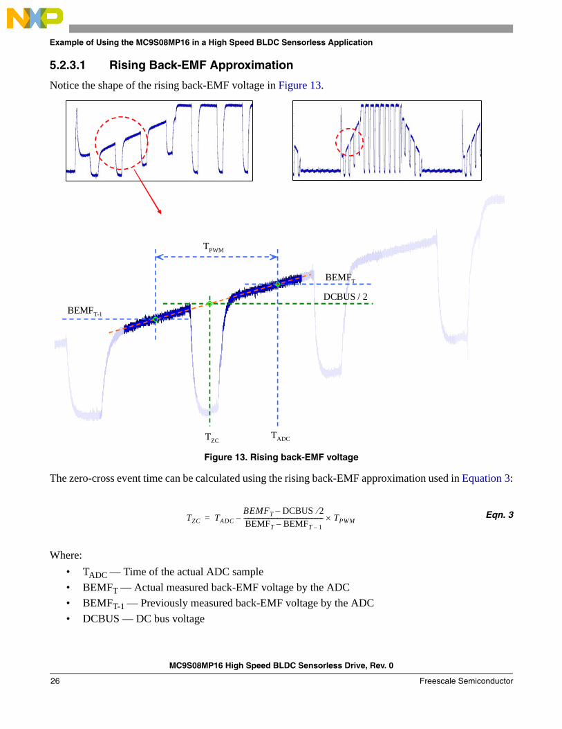
As described in Section 5.2.1, “Back-EMF Voltage Sensing,” on page 21, the back-EMF voltage is sensed every 50 s (once every PWM pulse). Therefore, the zero-cross event can be found with a 50s precision. This is very inaccurate in high speed applications, for example, if the commutation period takes only 200 s, then there are only four PWM periods during one commutation period, and a 50 s precision in finding a zero-cross event is poor. In that case, the approximation of the two back-EMF ADC samples can be used to calculate the zero-cross event more precisely. One back-EMF voltage ADC value just before the zero-cross event, and one back-EMF voltage ADC value just after the zero-cross event are needed to precisely re-calculate the zero-cross event. See Figure 13 and Figure 14. This approximation technique is implemented in the demo application. It depends on the actual rotor position if the currently measured back-EMF voltage is rising or falling, and for each case different calculations are used to approximate the two ADC samples.
MC9S08MP16 High Speed BLDC Sensorless Drive, Rev. 0
Freescale Semiconductor 25
Example of Using the MC9S08MP16 in a High Speed BLDC Sensorless Application
5.2.3.1 Rising Back-EMF Approximation
Notice the shape of the rising back-EMF voltage in Figure 13.
Figure 13. Rising back-EMF voltage
The zero-cross event time can be calculated using the rising back-EMF approximation used in Equation 3:
Eqn. 3
Where:
• TADC — Time of the actual ADC sample
• BEMFT — Actual measured back-EMF voltage by the ADC
• BEMFT-1 — Previously measured back-EMF voltage by the ADC
• DCBUS — DC bus voltage
DCBUS / 2
BEMFT
BEMFT-1
TADC
TPWM
TZC
TZC TADC
BEMFT DCBUS 2–
BEMFT BEMFT 1––---------------------------------------------------- TPWM–=
MC9S08MP16 High Speed BLDC Sensorless Drive, Rev. 0
Freescale Semiconductor26
Example of Using the MC9S08MP16 in a High Speed BLDC Sensorless Application
• TPWM — Period of the PWM pulse, equal to the period between the BEMFT and BEMFT-1 ADC samples
• TZC — Recalculated time of the zero-cross event
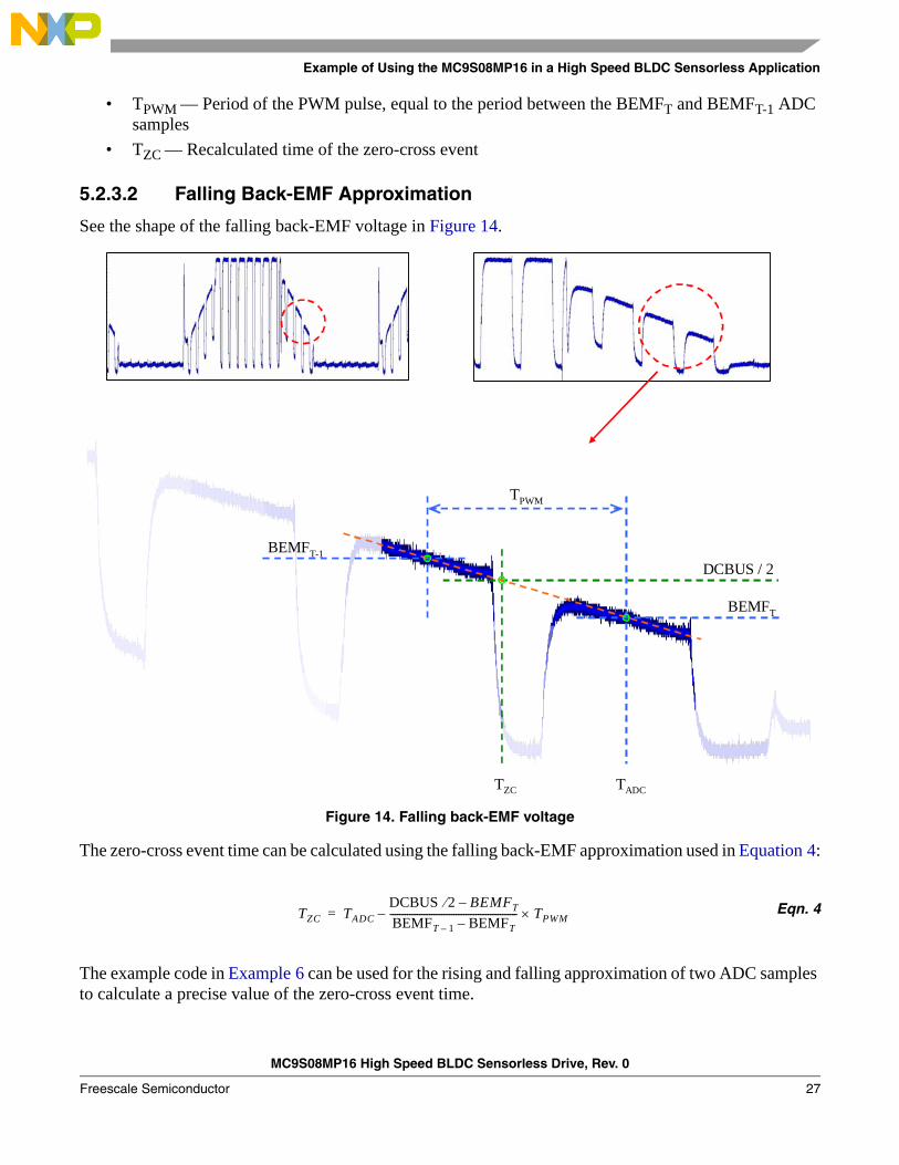
5.2.3.2 Falling Back-EMF Approximation
See the shape of the falling back-EMF voltage in Figure 14.
Figure 14. Falling back-EMF voltage
The zero-cross event time can be calculated using the falling back-EMF approximation used in Equation 4:
Eqn. 4
The example code in Example 6 can be used for the rising and falling approximation of two ADC samples to calculate a precise value of the zero-cross event time.
DCBUS / 2
BEMFT
BEMFT-1
TADC
TPWM
TZC
TZC TADC
DCBUS 2 BEMFT–
BEMFT 1– BEMFT–---------------------------------------------------- TPWM–=
MC9S08MP16 High Speed BLDC Sensorless Drive, Rev. 0
Freescale Semiconductor 27
Example of Using the MC9S08MP16 in a High Speed BLDC Sensorless Application
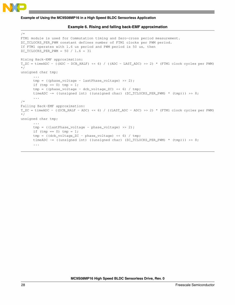
Example 6. Rising and falling back-EMF approximation
/*FTM1 module is used for Commutation timing and Zero-cross period measurement.ZC_TCLOCKS_PER_PWM constant defines number of FTM1 clocks per PWM period.If FTM1 operates with 1.6 us period and PWM period is 50 us, thenZC_TCLOCKS_PER_PWM = 50 / 1.6 = 31
Rising Back-EMF approximation:T_ZC = timeADC - ((ADC - DCB_HALF) << 6) / ((ADC - LAST_ADC) >> 2) * (FTM1 clock cycles per PWM)*/unsigned char tmp;
...tmp = ((phase_voltage - lastPhase_voltage) >> 2);if (tmp == 0) tmp = 1;tmp = ((phase_voltage - dcb_voltage_ZC) << 6) / tmp;timeADC -= ((unsigned int) ((unsigned char) (ZC_TCLOCKS_PER_PWM) * (tmp))) >> 8;...
/*Falling Back-EMF approximation:T_ZC = timeADC - ((DCB_HALF - ADC) << 6) / ((LAST_ADC - ADC) >> 2) * (FTM1 clock cycles per PWM)*/unsigned char tmp;
...tmp = ((lastPhase_voltage - phase_voltage) >> 2);if (tmp == 0) tmp = 1;tmp = ((dcb_voltage_ZC - phase_voltage) << 6) / tmp;timeADC -= ((unsigned int) ((unsigned char) (ZC_TCLOCKS_PER_PWM) * (tmp))) >> 8;...
MC9S08MP16 High Speed BLDC Sensorless Drive, Rev. 0
Freescale Semiconductor28
Example of Using the MC9S08MP16 in a High Speed BLDC Sensorless Application
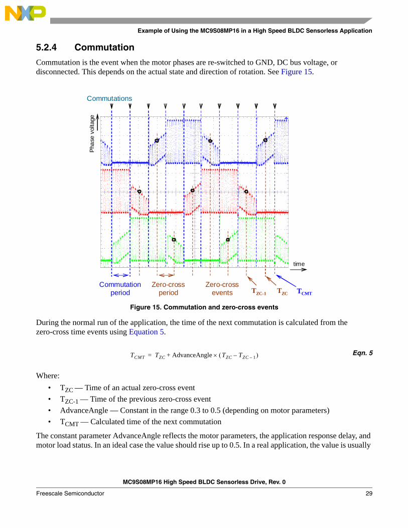
5.2.4 Commutation
Commutation is the event when the motor phases are re-switched to GND, DC bus voltage, or disconnected. This depends on the actual state and direction of rotation. See Figure 15.
Figure 15. Commutation and zero-cross events
During the normal run of the application, the time of the next commutation is calculated from the zero-cross time events using Equation 5.
Eqn. 5
Where:
• TZC — Time of an actual zero-cross event
• TZC-1 — Time of the previous zero-cross event
• AdvanceAngle — Constant in the range 0.3 to 0.5 (depending on motor parameters)
• TCMT — Calculated time of the next commutation
The constant parameter AdvanceAngle reflects the motor parameters, the application response delay, and motor load status. In an ideal case the value should rise up to 0.5. In a real application, the value is usually
Commutations
Commutationperiod
Zero-crossevents
Zero-crossperiod TZCTZC-1 TCMT
Pha
se v
olta
ge
time
TCMT TZC AdvanceAngle TZC TZC 1–– +=
MC9S08MP16 High Speed BLDC Sensorless Drive, Rev. 0
Freescale Semiconductor 29
Conclusion
in the range of 0.3 to 0.45 and is almost constant. The exact value is tuned during the application development. The example code in Example 7 can be used to calculate the time of the next commutation.
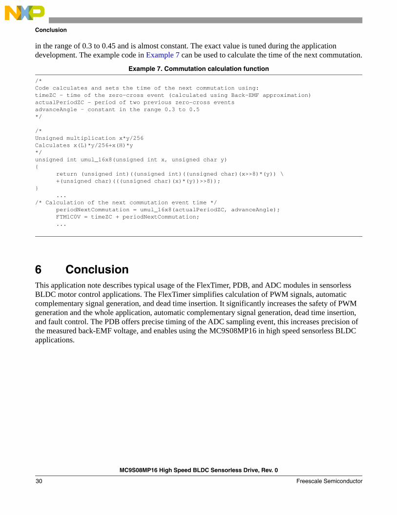
Example 7. Commutation calculation function
/*Code calculates and sets the time of the next commutation using:timeZC - time of the zero-cross event (calculated using Back-EMF approximation)actualPeriodZC - period of two previous zero-cross eventsadvanceAngle - constant in the range 0.3 to 0.5*/
/*Unsigned multiplication x*y/256Calculates x(L)*y/256+x(H)*y*/unsigned int umul_16x8(unsigned int x, unsigned char y){
return (unsigned int)((unsigned int)((unsigned char)(x>>8)*(y)) \+(unsigned char)(((unsigned char)(x)*(y))>>8));
}...
/* Calculation of the next commutation event time */periodNextCommutation = umul_16x8(actualPeriodZC, advanceAngle);FTM1C0V = timeZC + periodNextCommutation;...
6 ConclusionThis application note describes typical usage of the FlexTimer, PDB, and ADC modules in sensorless BLDC motor control applications. The FlexTimer simplifies calculation of PWM signals, automatic complementary signal generation, and dead time insertion. It significantly increases the safety of PWM generation and the whole application, automatic complementary signal generation, dead time insertion, and fault control. The PDB offers precise timing of the ADC sampling event, this increases precision of the measured back-EMF voltage, and enables using the MC9S08MP16 in high speed sensorless BLDC applications.
MC9S08MP16 High Speed BLDC Sensorless Drive, Rev. 0
Freescale Semiconductor30

Conclusion
MC9S08MP16 High Speed BLDC Sensorless Drive, Rev. 0
Freescale Semiconductor 31

Document Number: AN4142Rev. 010/2010
How to Reach Us:
Home Page:www.freescale.com
Web Support:http://www.freescale.com/support
USA/Europe or Locations Not Listed:Freescale Semiconductor, Inc.Technical Information Center, EL5162100 East Elliot RoadTempe, Arizona 85284+1-800-521-6274 or +1-480-768-2130www.freescale.com/support
Europe, Middle East, and Africa:Freescale Halbleiter Deutschland GmbHTechnical Information CenterSchatzbogen 781829 Muenchen, Germany+44 1296 380 456 (English)+46 8 52200080 (English)+49 89 92103 559 (German)+33 1 69 35 48 48 (French)www.freescale.com/support
Japan:Freescale Semiconductor Japan Ltd.HeadquartersARCO Tower 15F1-8-1, Shimo-Meguro, Meguro-ku,Tokyo 153-0064Japan0120 191014 or +81 3 5437 [email protected]
Asia/Pacific:Freescale Semiconductor China Ltd.Exchange Building 23FNo. 118 Jianguo RoadChaoyang DistrictBeijing 100022 China +86 10 5879 [email protected]
For Literature Requests Only:Freescale Semiconductor Literature Distribution Center1-800-441-2447 or 303-675-2140Fax: [email protected]
Information in this document is provided solely to enable system and software implementers to use Freescale Semiconductor products. There are no express or implied copyright licenses granted hereunder to design or fabricate any integrated circuits or integrated circuits based on the information in this document.
Freescale Semiconductor reserves the right to make changes without further notice to any products herein. Freescale Semiconductor makes no warranty, representation or guarantee regarding the suitability of its products for any particular purpose, nor does Freescale Semiconductor assume any liability arising out of the application or use of any product or circuit, and specifically disclaims any and all liability, including without limitation consequential or incidental damages. “Typical” parameters that may be provided in Freescale Semiconductor data sheets and/or specifications can and do vary in different applications and actual performance may vary over time. All operating parameters, including “Typicals”, must be validated for each customer application by customer’s technical experts. Freescale Semiconductor does not convey any license under its patent rights nor the rights of others. Freescale Semiconductor products are not designed, intended, or authorized for use as components in systems intended for surgical implant into the body, or other applications intended to support or sustain life, or for any other application in which the failure of the Freescale Semiconductor product could create a situation where personal injury or death may occur. Should Buyer purchase or use Freescale Semiconductor products for any such unintended or unauthorized application, Buyer shall indemnify and hold Freescale Semiconductor and its officers, employees, subsidiaries, affiliates, and distributors harmless against all claims, costs, damages, and expenses, and reasonable attorney fees arising out of, directly or indirectly, any claim of personal injury or death associated with such unintended or unauthorized use, even if such claim alleges that Freescale Semiconductor was negligent regarding the design or manufacture of the part.
RoHS-compliant and/or Pb-free versions of Freescale products have the functionality and electrical characteristics as their non-RoHS-compliant and/or non-Pb-free counterparts. For further information, see http://www.freescale.com or contact your Freescale sales representative.
For information on Freescale’s Environmental Products program, go to http://www.freescale.com/epp.
Freescale™ and the Freescale logo are trademarks of Freescale Semiconductor, Inc. All other product or service names are the property of their respective owners.© Freescale Semiconductor, Inc. 2010. All rights reserved.
Related Documents