Memory Built Memory Built-In Self In Self-Repair Repair Memory Built Memory Built In Self In Self Repair Repair Jin-Fu Li Ad dR li bl S (ARES) L b Advanced Reliable Systems (ARES) Lab. Department of Electrical Engineering National Central University Jhongli, Taiwan

Welcome message from author
This document is posted to help you gain knowledge. Please leave a comment to let me know what you think about it! Share it to your friends and learn new things together.
Transcript

Memory BuiltMemory Built--In SelfIn Self--RepairRepairMemory BuiltMemory Built In SelfIn Self Repair Repair
Jin-Fu Li Ad d R li bl S (ARES) L bAdvanced Reliable Systems (ARES) Lab.
Department of Electrical EngineeringNational Central University
Jhongli, Taiwan

Outline
IntroductionRedundancy OrganizationsBuilt-In Redundancy Analysis TechniquesBuilt-In Redundancy Analysis TechniquesBuilt-In Self-Repair TechniquesConclusions
Advanced Reliable Systems (ARES) Lab., EE. NCU Jin-Fu Li 2
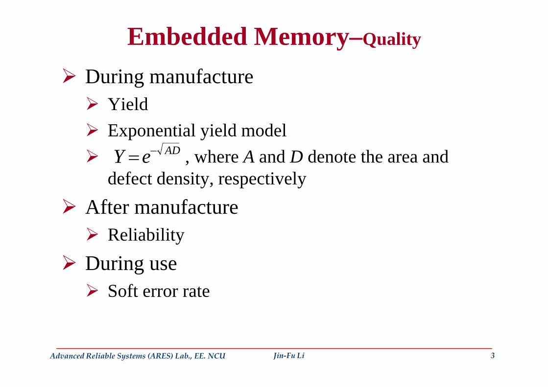
Embedded Memory–Quality
During manufactureYieldYieldExponential yield model
AD , where A and D denote the area and defect density, respectively
ADeY −=
After manufactureReliabilityReliability
During useSoft error rate
Advanced Reliable Systems (ARES) Lab., EE. NCU Jin-Fu Li 3

An Explosion in Embedded Memories Hundreds of memory cores in a complex chip is commonMemory cores usually represent a significant
ti f th hiportion of the chip area
RAMRAM
RAMRAM
RAM
RAMRAMRAM
RAM
RAM
RAM
Advanced Reliable Systems (ARES) Lab., EE. NCU Jin-Fu Li 4
AMD dual-core Opteron™ processor Intel dual-core Intanium processor (JSSC, 2006)

Memory Repair Repair is one popular technique for memory yield improvementyield improvementMemory repair consists of three basic steps
Test Redundancy analysisRedundancy analysisRepair delivery
Advanced Reliable Systems (ARES) Lab., EE. NCU Jin-Fu Li 5
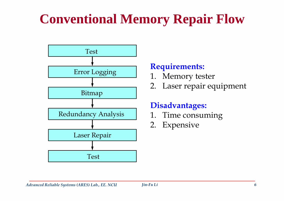
Conventional Memory Repair Flow
Test
Error LoggingRequirements:1 Memory tester
Bitmap
1. Memory tester2. Laser repair equipment
Redundancy AnalysisDisadvantages:1. Time consuming2 E i
Laser Repair2. Expensive
Test
Advanced Reliable Systems (ARES) Lab., EE. NCU Jin-Fu Li 6

Memory BISR Flow
FunctionRequired Circuit
BIST Built-In Self-Test Test
FunctionRequired Circuit
BISD Built-In Self-Diagnosis Fault Location
BIRA Built-In Redundancy-Analyzer Redundancy allocation
Reconfiguration Swap Defective Cells
Advanced Reliable Systems (ARES) Lab., EE. NCU Jin-Fu Li 7
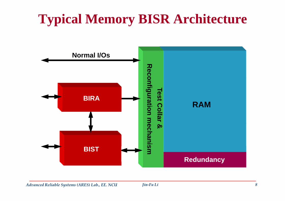
Typical Memory BISR Architecture
Normal I/Os
Reco
Normal I/Os
TestonfiguraBIRA
RAM
t Collar
ation m
BIRA
&echanissm
RedundancyBIST
Advanced Reliable Systems (ARES) Lab., EE. NCU Jin-Fu Li 8

Typical Memory BIST Architecture
Normal I/OsNormal I/Os
Tes
Test Controller
RAM
st Collar
Test PatternGenerator rGenerator
Comparator
Advanced Reliable Systems (ARES) Lab., EE. NCU Jin-Fu Li 9
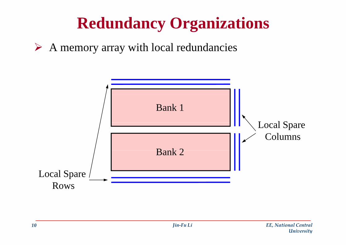
Redundancy Organizations A memory array with local redundancies
L l S
Bank 1
Local Spare Columns
B k 2
Local Spare
Bank 2
pRows
10 Jin-Fu Li EE, National Central University
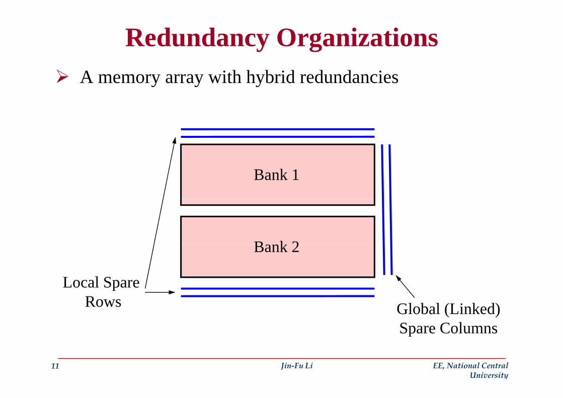
Redundancy Organizations A memory array with hybrid redundancies
Bank 1
B k 2
Local Spare
Bank 2
Global (Linked)Spare Columns
pRows
11 Jin-Fu Li EE, National Central University
p

Redundancy Organizations A memory array with hybrid redundancies
Bank 1 Bank 2
Bank 2 B k 2
Global (Linked)
Bank 2 Bank 2
LocalSpare Columns
( )Spare Rows
12 Jin-Fu Li EE, National Central University
p
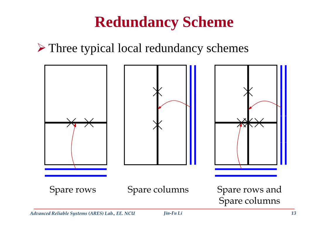
Redundancy SchemeThree typical local redundancy schemes
Spare rows Spare columns Spare rows and
Advanced Reliable Systems (ARES) Lab., EE. NCU Jin-Fu Li 13
Spare columns
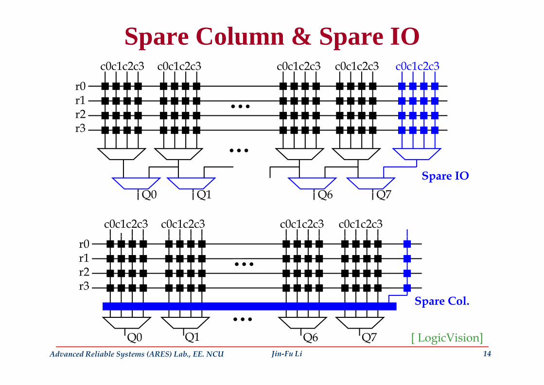
Spare Column & Spare IO c0c1c2c3 c0c1c2c3 c0c1c2c3 c0c1c2c3 c0c1c2c3
r0r1r2r3
Spare IOQ0 Q1 Q6 Q7
c0c1c2c3 c0c1c2c3 c0c1c2c3 c0c1c2c3
Q0 Q1 Q6 Q7
r0r1r2r3
Spare Col.
Advanced Reliable Systems (ARES) Lab., EE. NCU Jin-Fu Li 14
[ LogicVision]Q0 Q1 Q6 Q7

Reconfiguration Scheme
S
32 columns32 columnsSpare c
Spare co olumn
olumn
Sense Amplifier Sense Amplifier
Decoder
10 bit data
p p
Programming Module(Flash)
10-bit data
Advanced Reliable Systems (ARES) Lab., EE. NCU Jin-Fu Li 15
[M. Yarmaoka, et al., JSSC, 2002]

Types of Reconfiguration Schemes
Three kinds of reconfiguration techniquesf fi iSoft reconfigurationBy programming FFs to store repair informationy p g g p
Firm reconfigurationB i l til i t tBy programming non-volatile memories to store repair information
Hard (permanent) reconfigurationLaser-blown or electrically-blown polysilicon or y p ydiffusion fuses
Advanced Reliable Systems (ARES) Lab., EE. NCU Jin-Fu Li 16
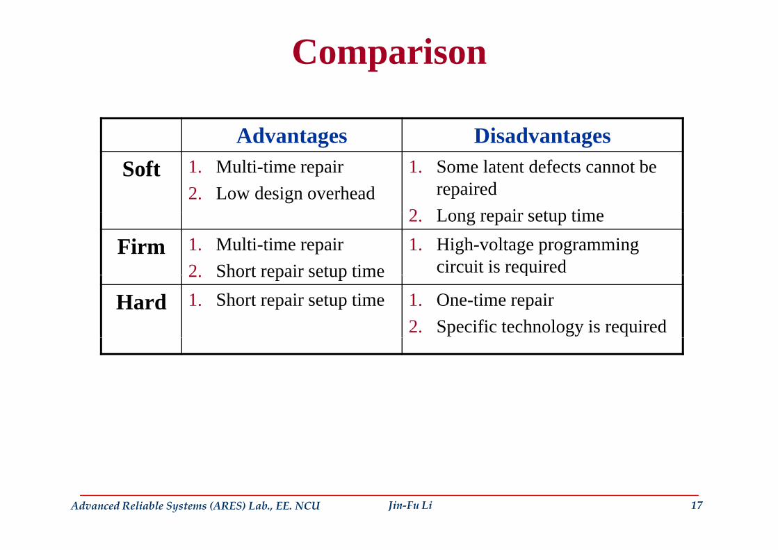
Comparison
Advantages DisadvantagesSoft 1. Multi-time repair
2. Low design overhead1. Some latent defects cannot be
repaired2 L i t ti2. Long repair setup time
Firm 1. Multi-time repair2 Short repair setup time
1. High-voltage programming circuit is required2. Short repair setup time q
Hard 1. Short repair setup time 1. One-time repair2. Specific technology is required
Advanced Reliable Systems (ARES) Lab., EE. NCU Jin-Fu Li 17
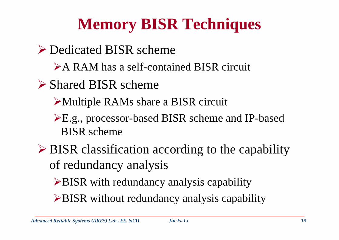
Memory BISR TechniquesDedicated BISR scheme
A RAM has a self contained BISR circuitA RAM has a self-contained BISR circuitShared BISR scheme
Multiple RAMs share a BISR circuitE g processor-based BISR scheme and IP-basedE.g., processor based BISR scheme and IP based BISR scheme
BISR l ifi ti di t th bilitBISR classification according to the capability of redundancy analysis
BISR with redundancy analysis capabilityBISR without redundancy analysis capability
Advanced Reliable Systems (ARES) Lab., EE. NCU Jin-Fu Li 18
BISR without redundancy analysis capability
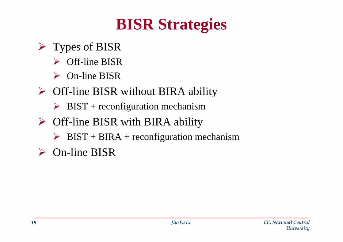
BISR Strategies Types of BISR
Off-line BISROn-line BISR
Off-line BISR without BIRA abilityOff line BISR without BIRA abilityBIST + reconfiguration mechanism
Off line BISR with BIRA abilityOff-line BISR with BIRA abilityBIST + BIRA + reconfiguration mechanism
O li BISROn-line BISR
19 Jin-Fu Li EE, National Central University
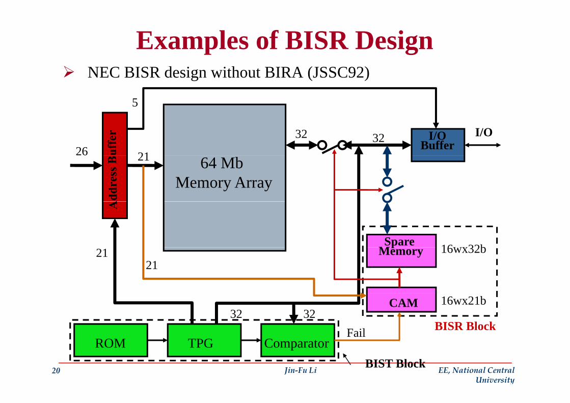
Examples of BISR DesignNEC BISR design without BIRA (JSSC92)
5
I/OBuffer
I/O
212632 32
64 MbMemory Array
21
SpareM 16 32bpMemory21
2116wx32b
ROM TPG C
CAM 16wx21b
BISR Block32 32
Fail
20 Jin-Fu Li EE, National Central University
ROM TPG ComparatorBIST Block

Examples of BISR DesignA BISR design (ITC98)
Data Input Bus
Main MemorySpare
Memory
Reconfiguration
Column Decoder
Redundancy Analysis
21 Jin-Fu Li EE, National Central University
ReconfigurationControl Unit
Redundancy Analysis Algorithm Information
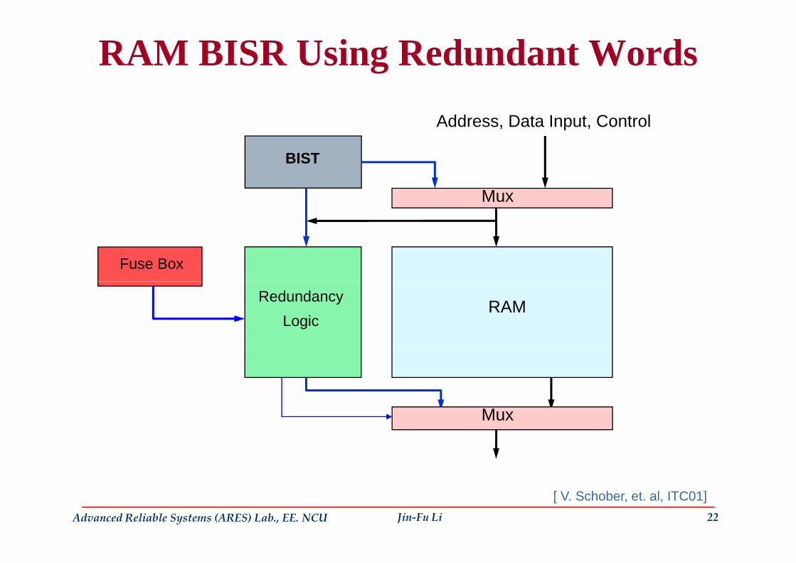
RAM BISR Using Redundant Words
BIST
Address, Data Input, Control
Mux
BIST
Fuse Box
RedundancyLogic
RAM
MMux
Advanced Reliable Systems (ARES) Lab., EE. NCU Jin-Fu Li 22
[ V. Schober, et. al, ITC01]

Redundancy Wrapper LogicThe redundancy logic consists of two basic components
Spare memory wordsSpare memory wordsLogic to program the address decoding
The address comparison is done in the redundancy logicThe address comparison is done in the redundancy logicThe address is compared to the addresses that are stored in the redundancy word linesredundancy word lines
An overflow bit identifies that there are more failing addresses than possible repair cellsaddresses than possible repair cells The programming of the faulty addresses is done during h BIST f h f b d ithe memory BIST or from the fuse box during memory
setup
Advanced Reliable Systems (ARES) Lab., EE. NCU Jin-Fu Li 23
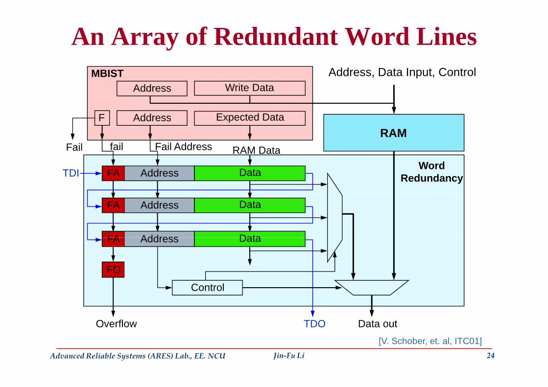
An Array of Redundant Word Lines
Address Write DataMBIST Address, Data Input, Control
Address Expected DataRAM
F
Fail fail Fail Address RAM Data
Address DataFA
Fail fail Fail Address RAM Data
TDIWord
Redundancy
Address DataFA
Address DataFA Address DataFA
FO
Control
TDO Data outOverflow
Advanced Reliable Systems (ARES) Lab., EE. NCU Jin-Fu Li 24
TDO Data outOverflow[V. Schober, et. al, ITC01]

Applications of Redundancy Logic
Faulty addresses can be streamed out after test completion Then the f se bo is blo ncompletion. Then the fuse box is blown accordingly in the last step of the test
This is called here hard repairThis is normally done at wafer level tests s o y do e w e eve es
Furthermore, the application can be started i di t l ft th BISTimmediately after the memory BIST passes
This is called here soft repair
Advanced Reliable Systems (ARES) Lab., EE. NCU Jin-Fu Li 25

Redundancy Word Line
WRAFail_addressFail DI Expected_data
Address DataFA TDOTDI
_Fail p _
Address DataFA TDOTDI
Comparator &
& Read
Expected_data, DOFail_addressFail
Advanced Reliable Systems (ARES) Lab., EE. NCU Jin-Fu Li 26
[V. Schober, et. al, ITC01]

One-Bit Fuse BoxO bi f b i f bi d fli flOne-bit fuse box contains a fuse bit and a scan flip flop for controlling and observing the fuse data
Test_Update=0: the chain of inverters is closed (The value is latched)T U d 1 i i ibl h i l d f TDOTest_Update=1: it is possible to set the internal node from TDOThe ports TDI and TDO are activated at scan mode
FRestScan 1
TDO
TDITest_Update
FRead
FGND t
FF10
Fout
FRest
FRead
Reset cycle to read out thefuse information
Fuse
out
FGND
Advanced Reliable Systems (ARES) Lab., EE. NCU Jin-Fu Li 27
Fuse Bit (FB) [V. Schober, et. al, ITC01]

Fuse BoxesThe fuse box can be connected to a scan register to stream in and out data during test and redundancy g yconfiguration
Fuse BoxReset
Update
FB FB FB
ScanFF
ScanFF
ScanFFTDI TDO
Fail A[0] A[N-1]
Advanced Reliable Systems (ARES) Lab., EE. NCU Jin-Fu Li 28
[V. Schober, et. al, ITC01]
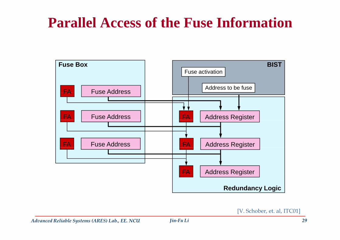
Parallel Access of the Fuse Information
BISTFuse Box
FA Fuse Address
Fuse activation
Address to be fuse
BISTFuse Box
FA Fuse Address
FA Address RegisterFA Fuse Address g
FA Address RegisterFA Fuse Address g
FA Address Registerg
Redundancy Logic
Advanced Reliable Systems (ARES) Lab., EE. NCU Jin-Fu Li 29
[V. Schober, et. al, ITC01]
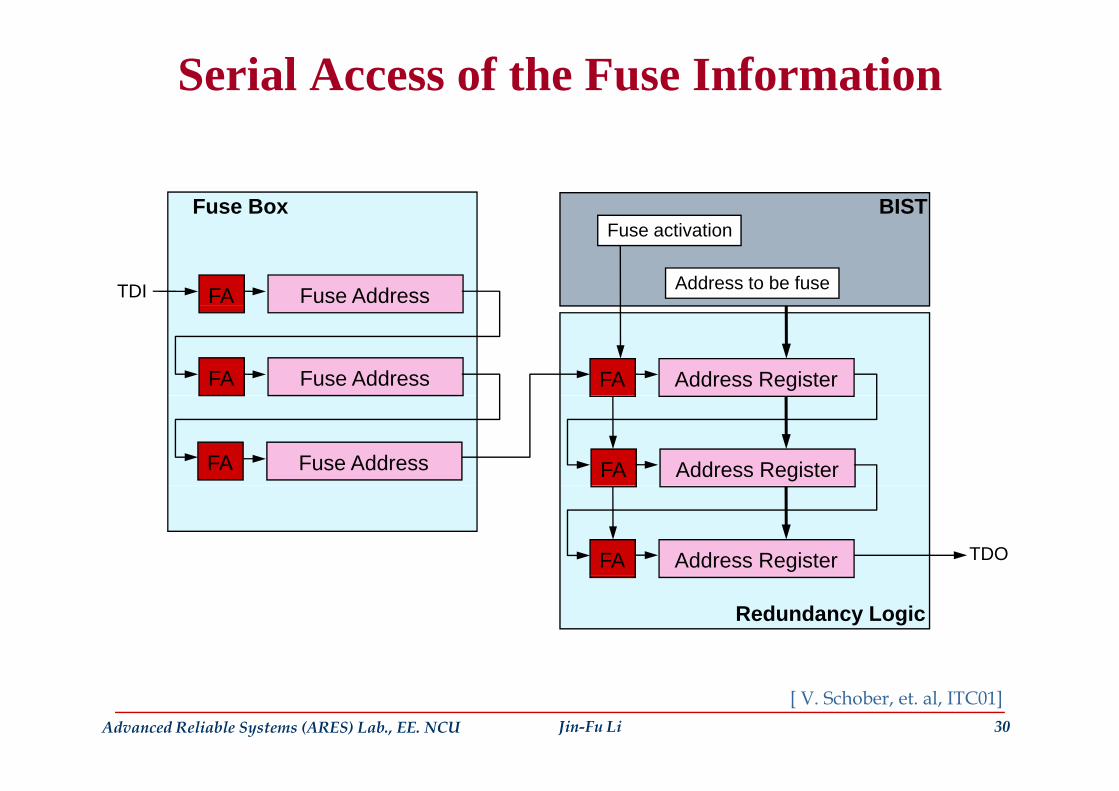
Serial Access of the Fuse Information
BISTFuse Box
FA Fuse Address
Fuse activation
Address to be fuseTDI
FA Address RegisterFA Fuse Address
FA Address RegisterFA Fuse Address
FA Address Register TDO
Redundancy Logic
Advanced Reliable Systems (ARES) Lab., EE. NCU Jin-Fu Li 30
[ V. Schober, et. al, ITC01]
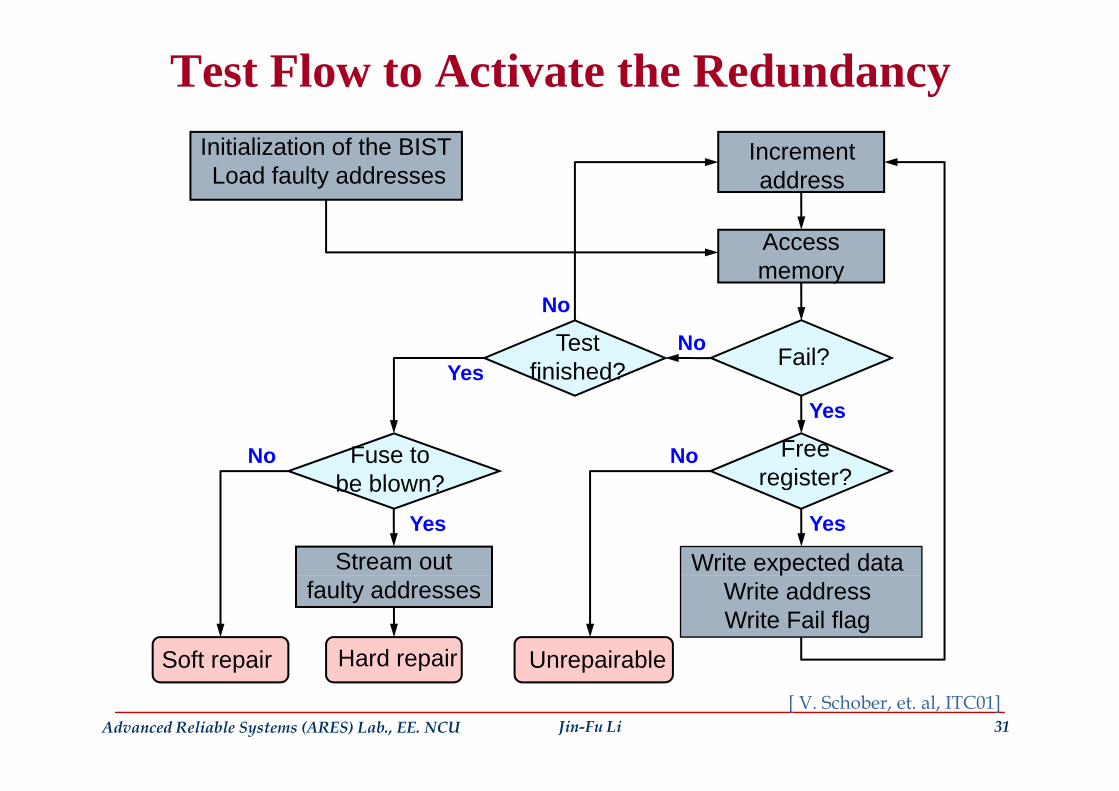
Test Flow to Activate the RedundancyInitialization of the BIST Load faulty addresses
Incrementaddress
Accessmemory
No
Testfinished? Fail?
No
NoYes
Freeregister?
Fuse tobe blown?
Yes
NoNoeg ste
Write expected data
be blown?
Stream out Yes Yes
pWrite addressWrite Fail flag
faulty addresses
Hard repairSoft repair Unrepairable
Advanced Reliable Systems (ARES) Lab., EE. NCU Jin-Fu Li 31[ V. Schober, et. al, ITC01]
Hard repairSoft repair Unrepairable

Redundancy AnalysisA repairable memory with 1D redundancyA repairable memory with 1D redundancy
Redundancy allocation is straightforward
i bl i h d dA repairable memory with 2D redundancyRedundancy analysis (redundancy allocation) is needed
Redundancy analysis problem Choose the minimum number of spare rows and columns that cover all the faulty cells
2 1 2 3
1
456
Advanced Reliable Systems (ARES) Lab., EE. NCU Jin-Fu Li 32
6
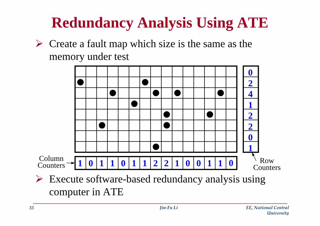
Redundancy Analysis Using ATE Create a fault map which size is the same as the memory under testy
0241222001
011001221101101 Row Column Counters
Execute software-based redundancy analysis using t i ATE
011001221101101 CountersCounters
33 Jin-Fu Li EE, National Central University
computer in ATE
Redundancy Analysis Using ATE d h d dHardware necessary to execute the redundancy
analysisA device image memory (or fault memory)
The size is the same as the memory under test
Counters that indicate the number of faults that occur in a row, or a column
A l h i l f b dApparently, the conventional software-based redundancy analysis algorithms are not adapted to be
li d i h h d d b b dd d i hrealized with hardware and be embedded into the SOCs
Hardware overhead is too large
Efficient built-in redundancy-analysis (BIRA)
34 Jin-Fu Li EE, National Central University
algorithms are required to be developed
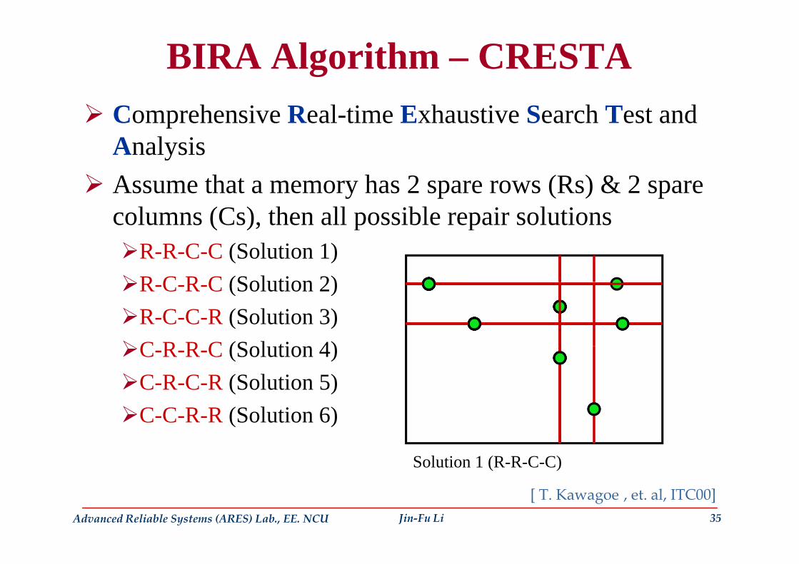
BIRA Algorithm – CRESTA Comprehensive Real-time Exhaustive Search Test and AnalysisAnalysisAssume that a memory has 2 spare rows (Rs) & 2 spare columns (Cs) then all possible repair solutionscolumns (Cs), then all possible repair solutions
R-R-C-C (Solution 1)R C R C (Solution 2)R-C-R-C (Solution 2)R-C-C-R (Solution 3)C R R C (S l ti 4)C-R-R-C (Solution 4)C-R-C-R (Solution 5)C C R R (S l ti 6)C-C-R-R (Solution 6)
Solution 1 (R-R-C-C)
Advanced Reliable Systems (ARES) Lab., EE. NCU Jin-Fu Li 35
[ T. Kawagoe , et. al, ITC00]

CRESTA Flow Chart Start
Test
NoFail ?
No
Yes
S1 S2 S3 S6
Finish ? NoYesYes
Result Output
Advanced Reliable Systems (ARES) Lab., EE. NCU Jin-Fu Li 36
End[T. Kawagoe , et. al, ITC00]

Basic Idea and Limitation of CRESTA Assume that there are m spare rows and n spare columns in a memory. Then a CRESTA repair analyzer y p ycontains C(m+n, m) sub-analyzers
E.g., if 2 spare rows and 2 spare columns are available, g , p p ,CRESTA will need C(4, 2)=6 sub-analyzers
Each sub-analyzer analyzes in-coming row/column y y gaddresses of faulty memory cells in parallel in a different repair strategy p gyBecause CRESTA tries all the possible repair strategies of spare resources it guarantees finding a solution for aof spare resources, it guarantees finding a solution for a repairable memory
37 Jin-Fu Li EE, National Central University

Basic Idea and Limitation of CRESTA Since CRESTA needs row address and column address of a faulty memory cell in order to check if the current y yfaulty memory cell can be repaired by previously allocated spare resources p
It is unable to handle at-speed multiple-bit failure occurring in a word-oriented memoryDetermine the number of spare columns needed for all failure bits in a word cannot be achieved in one cycle
In an at-speed BISR design, a column repair vector (CRV) is used to store column failure information for solving this problem
CRV is a column repair vector of the same size as the word width
38 Jin-Fu Li EE, National Central University
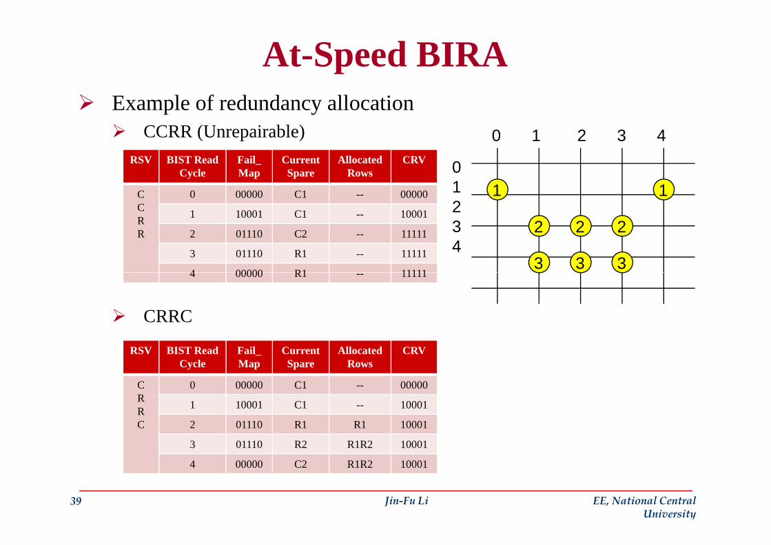
At-Speed BIRA Example of redundancy allocation
CCRR (Unrepairable) 0 1 2 3 4
1 1012
RSV BIST Read Cycle
Fail_Map
CurrentSpare
AllocatedRows
CRV
CC
0 00000 C1 -- 00000
1 10001 C1 100012 2 2
3 3 3
234
CRR
1 10001 C1 -- 10001
2 01110 C2 -- 11111
3 01110 R1 -- 11111
4 00000 R1 11111
CRRC
4 00000 R1 -- 11111
RSV BIST Read Cycle
Fail_Map
CurrentSpare
AllocatedRows
CRV
CR
0 00000 C1 -- 00000RRC
1 10001 C1 -- 10001
2 01110 R1 R1 10001
3 01110 R2 R1R2 10001
39 Jin-Fu Li EE, National Central University
4 00000 C2 R1R2 10001

At-Speed BIRA Implementation
BIST Controller
RestartFail/Success
BIST Controller
MemoryMemoryUnder Test
BISRA Repair DataBISRAController
Repair DataRepairable
In the BISRA, all C(m+n, m) analysis engines or just one engine can be implementedIn one engine scheme, update the repair strategy if the current repair strategy fails and then re-run BIST and try th t i t t
40 Jin-Fu Li EE, National Central University
the next repair strategy
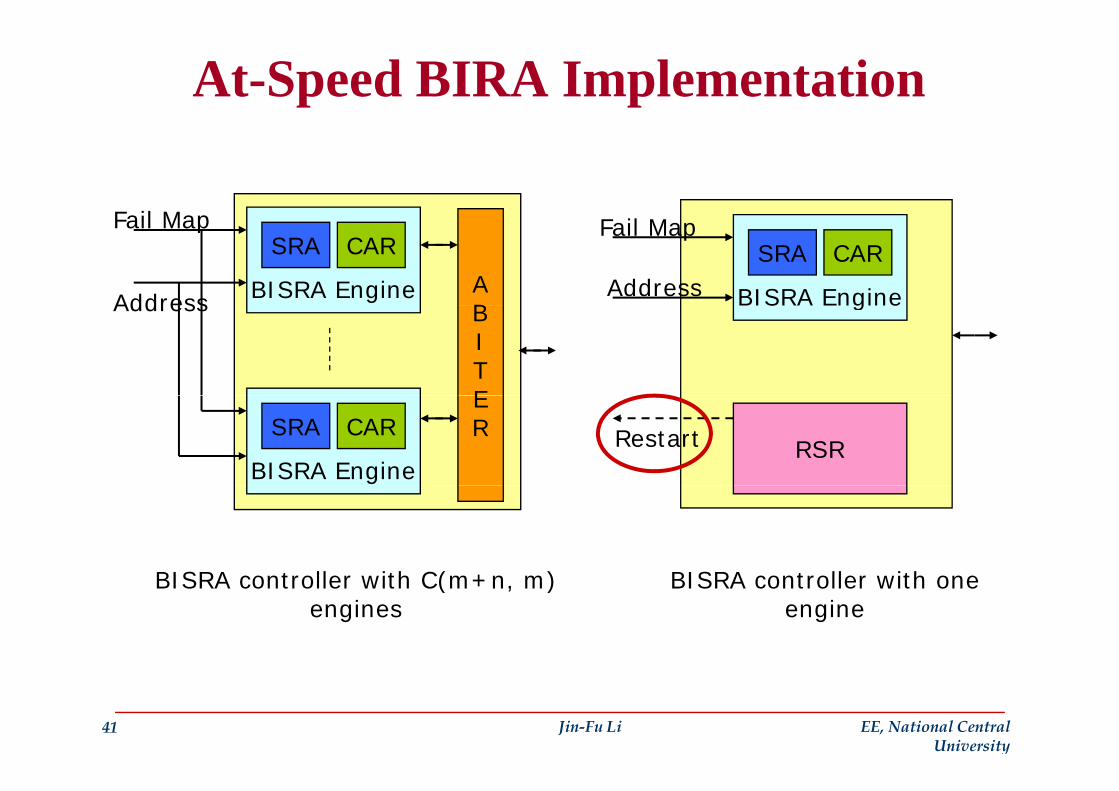
At-Speed BIRA Implementation
Fail Map
BISRA Engine
SRA CARAB
Fail Map
Address BISRA Engine
SRA CARFail Map
AddressBITE
Address g
BISRA Engine
SRA CARER
RSRRestart
BISRA cont olle ith C(m+n m) BISRA cont olle ith one BISRA controller with C(m+n, m) engines
BISRA controller with one engine
41 Jin-Fu Li EE, National Central University
At-Speed BIRA ImplementationSpare Resource Allocation (SRA): allocates either a spare row or a spare column according to its repair strategyControl and Report (CAR): checks if this repair strategy fails
If not, it will report the repair data, such as faulty row addresses and CRV to BISRA controllerCRV, to BISRA controller
Repair Strategy Reconfiguration (RSR) block: updates the repair strategy and sends a “restart” signal to BIST controllerrepair strategy and sends a restart signal to BIST controller
42 Jin-Fu Li EE, National Central University
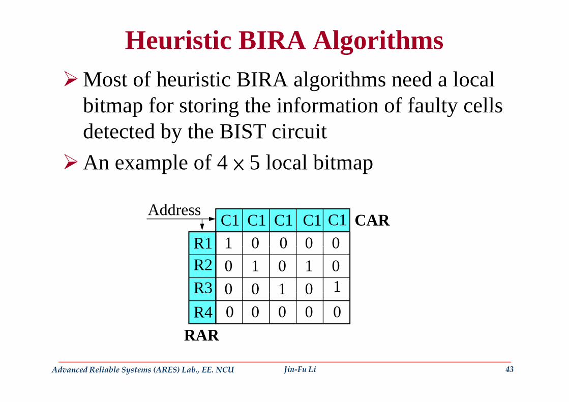
Heuristic BIRA AlgorithmsMost of heuristic BIRA algorithms need a local bitmap for storing the information of faulty cellsbitmap for storing the information of faulty cells detected by the BIST circuitA l f 4 5 l l biAn example of 4 × 5 local bitmap
Address C1 C1 C1 C1 C1R1
CAR1 0 0 0 0R1
R2R3
1 0 01 1
110
0 000
0 0 0R3R4
RAR
10 0 00 0000
Advanced Reliable Systems (ARES) Lab., EE. NCU Jin-Fu Li 43
RAR

A BIRA Flow for Performing Heuristic RAsSTART
BIST
Fail?No
YesLocal Bitmap
Yes
Full?UpdateBitmap
No
YRedundancy
Allocation
pYes
Advanced Reliable Systems (ARES) Lab., EE. NCU Jin-Fu Li 44
Allocation
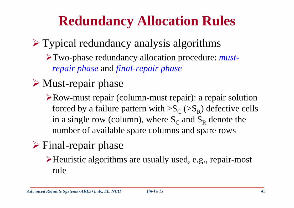
Redundancy Allocation RulesTypical redundancy analysis algorithms
Two phase redundancy allocation procedure: mustTwo-phase redundancy allocation procedure: must-repair phase and final-repair phase
M t i hMust-repair phaseRow-must repair (column-must repair): a repair solution forced by a failure pattern with >SC (>SR) defective cells in a single row (column), where SC and SR denote the
b f il bl l dnumber of available spare columns and spare rows
Final-repair phaseHeuristic algorithms are usually used, e.g., repair-most rule
Advanced Reliable Systems (ARES) Lab., EE. NCU Jin-Fu Li 45

NTHU/ADMtek BISR SchemeR d d i iRedundancy organization
SEG0
SEG1
SCG
0
SCG
1
SR0SR1
46 Jin-Fu Li EE, National Central University
SR: Spare Row; SCG: Spare Column Group; SEG: Segment

Dedicated BISR: NTHU/ADMtek BISR SchemeBISR block diagramBISR block diagram
D
Main Memory
Wrap
A
y
BIRA
pper
MAO
Spare MemoryBISTPOR
47 Jin-Fu Li EE, National Central University
MAO: mask address output; POR: power-on reset

BISR FlowPower-on BISR procedure
Power On
BIST Test Spare Row & Column BIRAError information
Power On
BIST Test Spare Row & Column BIRA
C iBIST Test Main Memory BIRA
Error information
Continue
Masked address
BIRAAddress
RemappingReduced address space
48 Jin-Fu Li EE, National Central University
Address
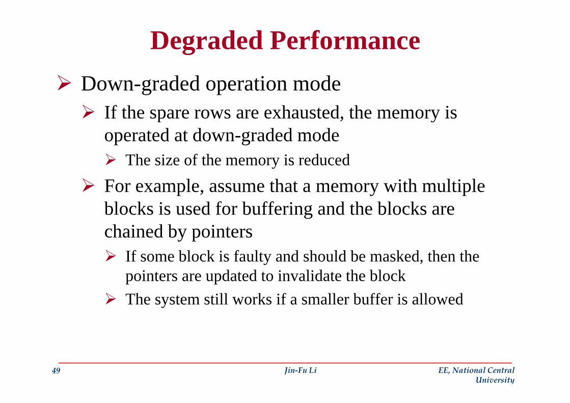
Degraded PerformanceDown-graded operation mode
If the spare rows are exhausted the memory isIf the spare rows are exhausted, the memory is operated at down-graded mode
Th i f th i d dThe size of the memory is reduced
For example, assume that a memory with multiple bl k i d f b ff i d h bl kblocks is used for buffering and the blocks are chained by pointers
If some block is faulty and should be masked, then the pointers are updated to invalidate the blockThe system still works if a smaller buffer is allowed
49 Jin-Fu Li EE, National Central University
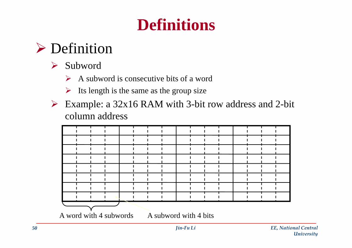
DefinitionsDefinition
SubwordSubwordA subword is consecutive bits of a wordIts length is the same as the group size
Example: a 32x16 RAM with 3-bit row address and 2-bit column address
50 Jin-Fu Li EE, National Central University
A subword with 4 bitsA word with 4 subwords

BIRA AlgorithmRow-repair rules
To reduce the complexity we use two row-repair rulesTo reduce the complexity, we use two row repair rulesA row has multiple faulty subwordsMultiple faulty subwords with the same column address and different row addresses
Examples:
subword subword
51 Jin-Fu Li EE, National Central University

BIRA ProcedureBIRA procedure
Run BIST StopDoneRun BIST Stop
Detects a fault
M tCheck Row-Repair Rules Met
Not met
Repair-Most Rules
Check Available Spare Rows
Export Faulty Row Address
No available spare row
52 Jin-Fu Li EE, National Central University
Export Faulty Row Address
Analysis of Repair RateRepair rate analysis
Repair rateThe ratio of the number of repaired memories to the number of defective memories
A simulator has been implemented to estimate the repair rate of the proposed BISR scheme [Huang, et al.,
MTDT, 2002]
Industrial case:SRAM size: 8Kx64# of injected random faults: 1~10# of injected random faults: 1 10# of memory samples: 534RA algorithms: proposed and exhaustive search
53 Jin-Fu Li EE, National Central University
RA algorithms: proposed and exhaustive search algorithms
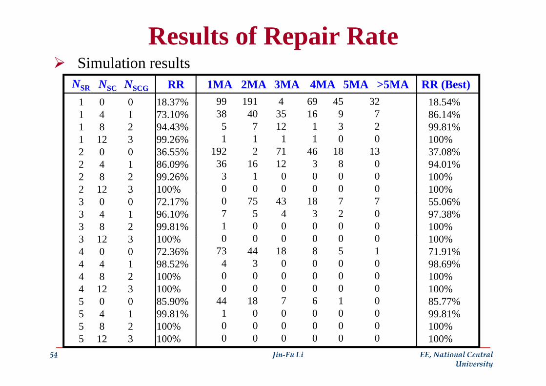
Results of Repair RateSimulation resultsSimulation results
NSR NSC NSCG RR 1MA 2MA 3MA 4MA 5MA >5MA RR (Best)18.37%1 0 0 99 191 4 69 45 32 18.54%8.37%73.10%94.43%99.26%36 55%
0 01 4 11 8 21 12 32 0 0
38 40 35 16 9 7 5 7 12 1 3 2 1 1 1 1 0 0
192 2 71 46 18 13
8.5 %86.14%99.81%100%37 08%36.55%
86.09%99.26%100%
2 0 02 4 12 8 22 12 3
192 2 71 46 18 1336 16 12 3 8 03 1 0 0 0 00 0 0 0 0 0
37.08%94.01%100%100%
72.17%96.10%99.81%100%
3 0 03 4 13 8 23 12 3
0 75 43 18 7 7 7 5 4 3 2 0 1 0 0 0 0 00 0 0 0 0 0
55.06%97.38%100%100%100%
72.36%98.52%100%
3 12 34 0 04 4 14 8 2
0 0 0 0 0 073 44 18 8 5 14 3 0 0 0 00 0 0 0 0 0
100%71.91%98.69%100%
100%85.90%99.81%100%
4 12 35 0 05 4 15 8 2
0 0 0 0 0 044 18 7 6 1 01 0 0 0 0 00 0 0 0 0 0
100%85.77%99.81%100%
54 Jin-Fu Li EE, National Central University
100%100%
5 8 25 12 3
0 0 0 0 0 00 0 0 0 0 0
100%100%

Test ChipLayout view of the repairable SRAM
Technology: 0 25umTechnology: 0.25umSRAM area: 6.5 mm2
BISR area : 0.3 mm2
S 0 3 2Spare area : 0.3 mm2
HOspare: 4.6%HObisr: 4.6%Repair rate: 100% (if # random faults is no more than 10)
Redundancy: 4 spare rows and 2 spare column groupsG i 4
55 Jin-Fu Li EE, National Central University
Group size: 4
Shared BISR TechniquesA complex SOC usually has many RAMs with different sizesdifferent sizesEach repairable RAM has a dedicated BISR circuit
Area cost is highgIf a BISR circuit can be shared by multiple RAMs, then the area cost of the BISR circuit can drasticallythen the area cost of the BISR circuit can drastically be reduced
h d h iShared BISR techniquesReconfigurable BISR or IP-based BISR technique
Advanced Reliable Systems (ARES) Lab., EE. NCU Jin-Fu Li 56

NCU/FTC BISR SchemeReconfigurable BISR scheme for multiple RAMs
RAM 1 RAM 2 RAM N-1
Wrapper Wrapper Wrapper
BIST ReBIRA ReBISR
RSO Shift_en
Register
FuseTDILD Fuse Group
TDO
Advanced Reliable Systems (ARES) Lab., EE. NCU Jin-Fu Li 57
[T. W. Tseng, et. al, ITC06]Fuse p

Repair Process
Test & Repair Normal Operation
BIST Power-On
BIRA Repair Signature Setup
Load Repair Signatures into the
Fuse GroupNormal Access
Fuse Group
Pre-Fuse Testing
Program Fuse
Advanced Reliable Systems (ARES) Lab., EE. NCU Jin-Fu Li 58

Test and Repair Mode
RAM 1 RAM 2 RAM N 1RAM 1
Wrapper
RAM 2
Wrapper
RAM N-1
Wrapper
BIST ReBIRABIST ReBIRA
RSO Shift en
ReBISR
RegisterTDI
_
TDO
FuseTDILD Fuse Group
Advanced Reliable Systems (ARES) Lab., EE. NCU Jin-Fu Li 59

Normal Mode
RAM 1 RAM 2 RAM N 1RAM 1
Wrapper
RAM 2
Wrapper
RAM N-1
Wrapper
BIST ReBIRABIST ReBIRA
RSO Shift en
ReBISR
RegisterTDI
_
TDO
FuseTDILD Fuse Group
Advanced Reliable Systems (ARES) Lab., EE. NCU Jin-Fu Li 60

NCU/FTC BISR SchemeReconfigurable BIRA architecture
Fail_hMulti faults
BIRA_en
FSM
_Syndrome
n
Multi-faultsDetector k
Test_done
Hold_l
Syndrome Encoder
Unrepairable
Shift_enBitmap
AddressRemapping TDIAddress
IO_Col
Ar+AcRemapping
registersMasker
Advanced Reliable Systems (ARES) Lab., EE. NCU Jin-Fu Li 61
[T. W. Tseng, et. al, ITC06]

Evaluation of Repair EfficiencyRepair rate
The ratio of the number of defective memories to theThe ratio of the number of defective memories to the number of repaired memories
A i l t i l t d t i l t thA simulator was implemented to simulate the repair rate [R.-F. Huang, et. al, IEEE D&T, 2005 (accepted)
Simulation setupSimulated memory size: 4096x128Simulated memory size: 4096x128Simulated memory samples: 500Poisson defect distribution is assumedOriginal yield is about 60%
Advanced Reliable Systems (ARES) Lab., EE. NCU Jin-Fu Li 62
g y
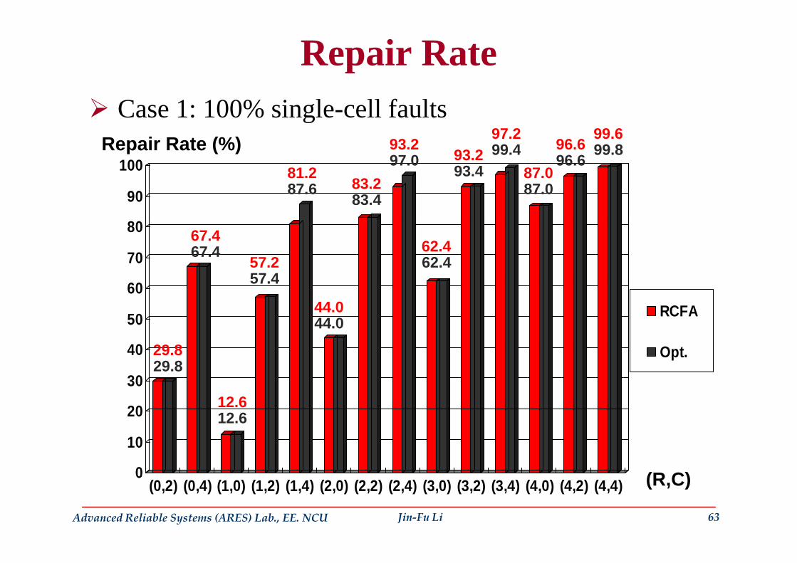
Repair RateCase 1: 100% single-cell faults
Repair Rate (%) 93.293 2
97.296.6
99.699.4 99.8
90
100p ( )
81.283.2
93.287.0
87.683.4
97.093.4
99.4
87.0
96.699.8
70
80 67.4
57.262.467.4
57.462.4
40
50
60RCFA
29 8
44.0
57.4
44.0
20
30
40 Opt.29.8
12.6
29.8
0
10
20
(R C)
12.6
Advanced Reliable Systems (ARES) Lab., EE. NCU Jin-Fu Li 63
0(0,2) (0,4) (1,0) (1,2) (1,4) (2,0) (2,2) (2,4) (3,0) (3,2) (3,4) (4,0) (4,2) (4,4) (R,C)

Repair RateCase 2: 50% single-cell faults, 20% faulty rows, 20% faulty columns, and 10% column twin-bit faults
96 6 98 8
90
100
Repair Rate (%)
85.8
93.8 92.898.2
86.6
96.4 99.881.2 82.0
92.4 89.896.6
86.6
94.8 98.8
70
80
67.0
85.8 82.2
61 8
86.6
67.057 4
61.8
50
60
RCFA
57.8
44 0
61.857.4
44.0
30
40 Opt.
28.2
44.028.2
10
2012.412.4
Advanced Reliable Systems (ARES) Lab., EE. NCU Jin-Fu Li 64
0(0,2) (0,4) (1,0) (1,2) (1,4) (2,0) (2,2) (2,4) (3,0) (3,2) (3,4) (4,0) (4,2) (4,4) (R,C)
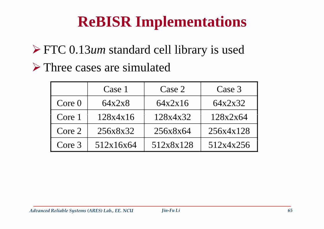
ReBISR Implementations
FTC 0.13um standard cell library is usedThree cases are simulated
Case 1 Case 2 Case 3Case 1 Case 2 Case 3 Core 0 64x2x8 64x2x16 64x2x32C 1 128 4 16 128 4 32 128 2 64Core 1 128x4x16 128x4x32 128x2x64Core 2 256x8x32 256x8x64 256x4x128Core 3 512x16x64 512x8x128 512x4x256
Advanced Reliable Systems (ARES) Lab., EE. NCU Jin-Fu Li 65
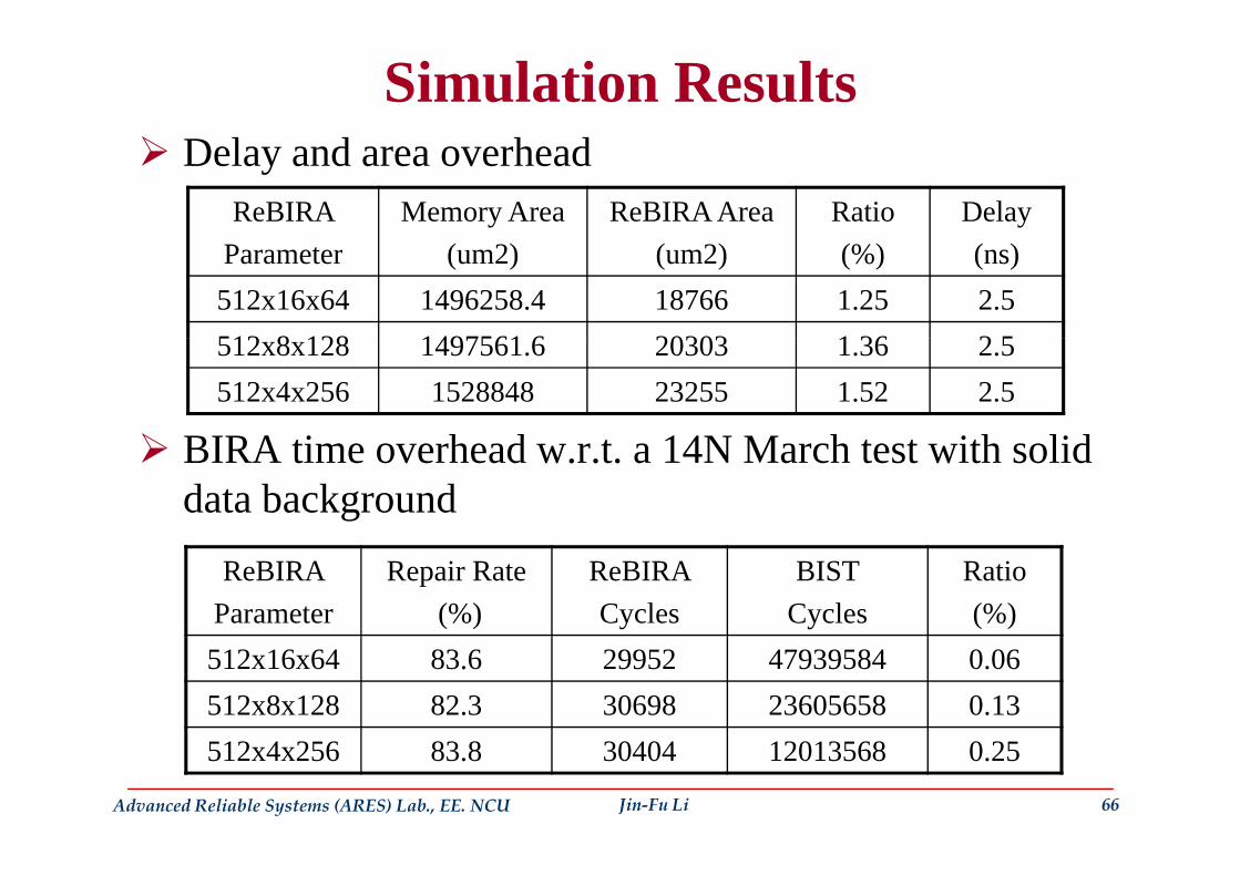
Simulation ResultsD l d h dDelay and area overhead
ReBIRA Memory Area ReBIRA Area Ratio Delay Parameter (um2) (um2) (%) (ns)512x16x64 1496258.4 18766 1.25 2.5512 8 128 1497561 6 20303 1 36 2 5
BIRA i h d 14N M h i h lid
512x8x128 1497561.6 20303 1.36 2.5512x4x256 1528848 23255 1.52 2.5
BIRA time overhead w.r.t. a 14N March test with solid data background
ReBIRA Parameter
Repair Rate(%)
ReBIRA Cycles
BIST Cycles
Ratio (%)
512x16x64 83.6 29952 47939584 0.06512x8x128 82.3 30698 23605658 0.13
Advanced Reliable Systems (ARES) Lab., EE. NCU Jin-Fu Li 66
512x4x256 83.8 30404 12013568 0.25
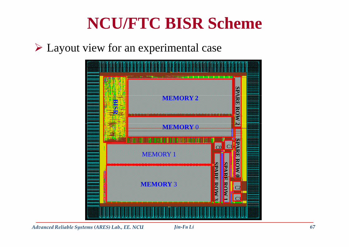
NCU/FTC BISR SchemeLayout view for an experimental case
SPA
MEMORY 2
AR
E R
OW
2
BISR
MEMORY 0
SPAR
2
C0 C1
MEMORY 1
RE
RO
W 0
SPAR
ESPA
RE
MEMORY 3
E R
OW
3E
RO
W 1
C2
C3
Advanced Reliable Systems (ARES) Lab., EE. NCU Jin-Fu Li 67
Infrastructure IPWhat is Infrastructure IP
Unlike the functional IP cores used in SOCs theUnlike the functional IP cores used in SOCs, the infrastructure IP cores do not add to the main functionality of the chip Rather they are intended tofunctionality of the chip. Rather, they are intended to ensure the manufacturability of the SOC and to achieve lifetime reliabilityachieve lifetime reliability
Examples of such infrastructure IPsProcess monitoring IP, test & repair IP, diagnosis IP, timing measurement IP, and fault tolerance IP
Advanced Reliable Systems (ARES) Lab., EE. NCU Jin-Fu Li 68
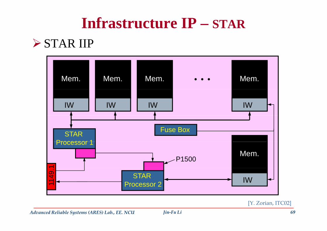
Infrastructure IP – STARSTAR IIP
Mem. Mem. Mem. Mem.
IW IW IW IW
STARProcessor 1
Fuse Box
Mem.Processor 1
1
P1500
IWSTARProcessor 211
49.1
Advanced Reliable Systems (ARES) Lab., EE. NCU Jin-Fu Li 69
[Y. Zorian, ITC02]

Infrastructure IP – STAR
The infrastructure IP is comprised of a number of hardware components, includingp , g
A STAR processor, a fuse box, and intelligent wrappers (IWs)
The STAR ProcessorPerforms all appropriate test & repair coordination of a STAR memoryIt is programmed by a set of instructions to control the operation of the internal modulesthe operation of the internal modules
The Intelligent WrapperAdd t i t d t t dAddress counters, registers, data comparators and multiplexers
Advanced Reliable Systems (ARES) Lab., EE. NCU Jin-Fu Li 70

Infrastructure IP – Repair Strategies
Hard Repair
i d
repaired
Soft Repairunrepaired
i d
Combinational Repair
repaired
P d d
Powered upunrepaired
Combinational Repair Powered down
repaired Reliability failureHard failuresCumulative Repair
unrepaired
p y f
Powered down
Hard failuresrepaired
repairedprogressivelyrepaired
progressivelyrepaired
71 Jin-Fu Li EE, National Central University
unrepairedrepaired
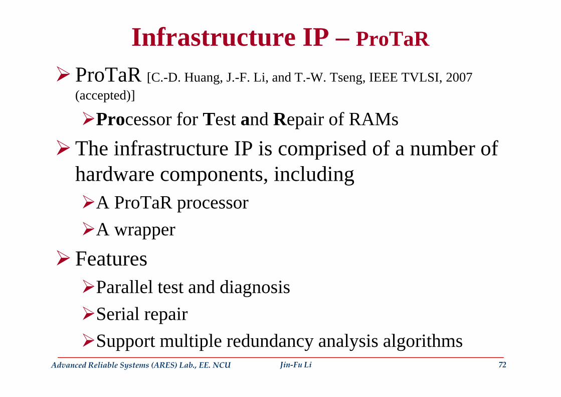
Infrastructure IP – ProTaR
ProTaR [C.-D. Huang, J.-F. Li, and T.-W. Tseng, IEEE TVLSI, 2007 (accepted)]
Processor for Test and Repair of RAMsThe infrastructure IP is comprised of a number ofThe infrastructure IP is comprised of a number of hardware components, including
A P T RA ProTaR processor A wrapper
FeaturesParallel test and diagnosisParallel test and diagnosisSerial repair
Advanced Reliable Systems (ARES) Lab., EE. NCU Jin-Fu Li 72
Support multiple redundancy analysis algorithms
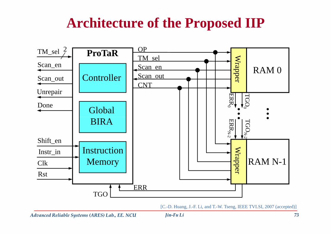
Architecture of the Proposed IIP
ProTaRTM_sel
Scan en
Wr
OPTM_sel
2
ControllerScan_en
Scan_out
U irapper
RAM 0Scan_enScan_outCNT
Global
Unrepair
Done
TGO
0
ERR
0
BIRA
Shift en
TGO
N-2
ERR
N-2
InstructionMemory
_Instr_inClk
Wrappe RAM N-1
Rst
er
ERRTGO
Advanced Reliable Systems (ARES) Lab., EE. NCU Jin-Fu Li 73
[C.-D. Huang, J.-F. Li, and T.-W. Tseng, IEEE TVLSI, 2007 (accepted)]
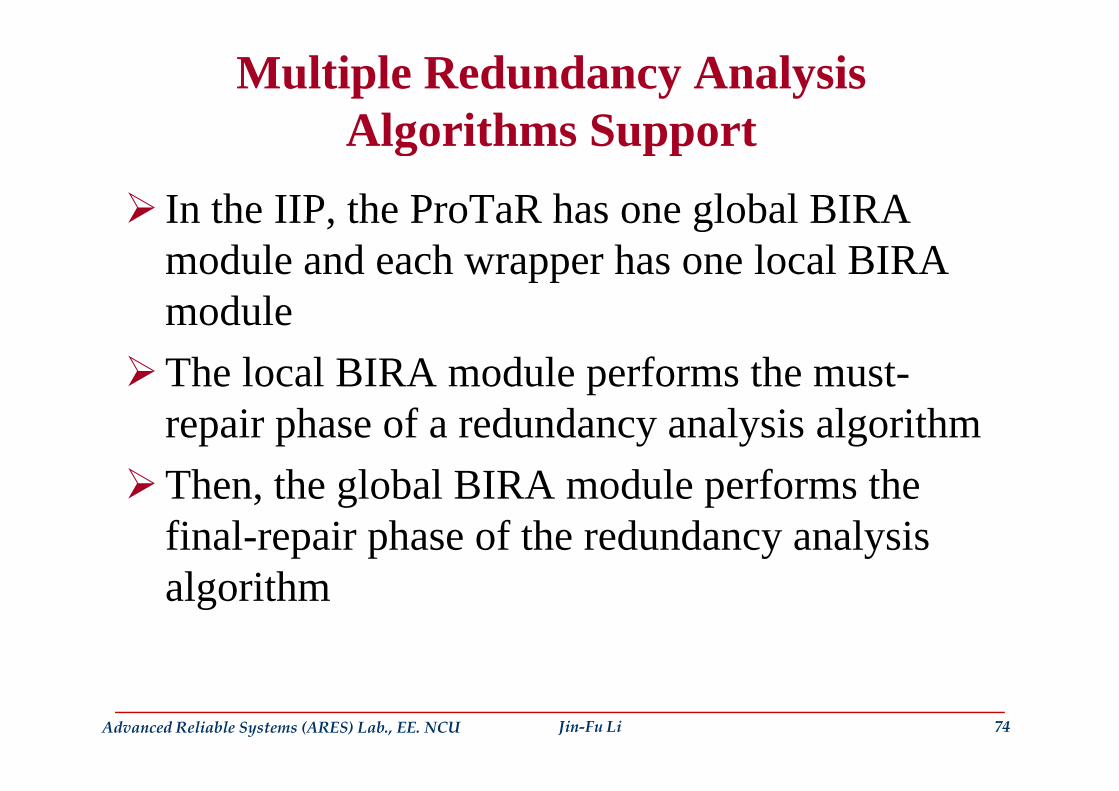
Multiple Redundancy Analysis Algorithms SupportAlgorithms Support
In the IIP the ProTaR has one global BIRAIn the IIP, the ProTaR has one global BIRA module and each wrapper has one local BIRA mod lemoduleThe local BIRA module performs the must-repair phase of a redundancy analysis algorithmThen the global BIRA module performs theThen, the global BIRA module performs the final-repair phase of the redundancy analysis l i halgorithm
Advanced Reliable Systems (ARES) Lab., EE. NCU Jin-Fu Li 74
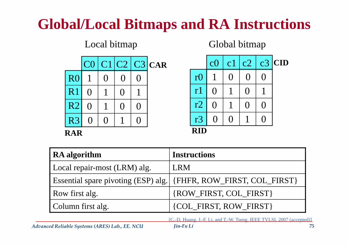
Global/Local Bitmaps and RA Instructions
c0 c1 c2 c3 CID
Global bitmap
C0 C1 C2 C3 CAR
Local bitmap
r0r1
1 0 01 10
00
C0 C1 C2 C3R0R1
CAR
1 0 01 10
00
r2r3
00 1 00 010
R2R3
1 1000
0 1 00 010
RIDR3
RAR0 010
RA algorithm InstructionsLocal repair-most (LRM) alg. LRME ti l i ti (ESP) l {FHFR ROW FIRST COL FIRST}Essential spare pivoting (ESP) alg. {FHFR, ROW_FIRST, COL_FIRST}Row first alg. {ROW_FIRST, COL_FIRST}Column first alg {COL FIRST ROW FIRST}
Advanced Reliable Systems (ARES) Lab., EE. NCU Jin-Fu Li 75
Column first alg. {COL_FIRST, ROW_FIRST}[C.-D. Huang, J.-F. Li, and T.-W. Tseng, IEEE TVLSI, 2007 (accepted)]
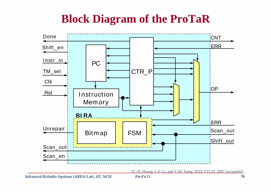
Block Diagram of the ProTaRDone
Shift_en
CNT
ERR
PCCTR P
Instr_in
TM_sel _
Instruction
Clk
Rst OP
InstructionMemory
BIRA
Bitmap FSMUnrepair
Shift t
Scan_outERR
Scan_en
Scan_outShift_out
Advanced Reliable Systems (ARES) Lab., EE. NCU Jin-Fu Li 76[C.-D. Huang, J.-F. Li, and T.-W. Tseng, IEEE TVLSI, 2007 (accepted)]
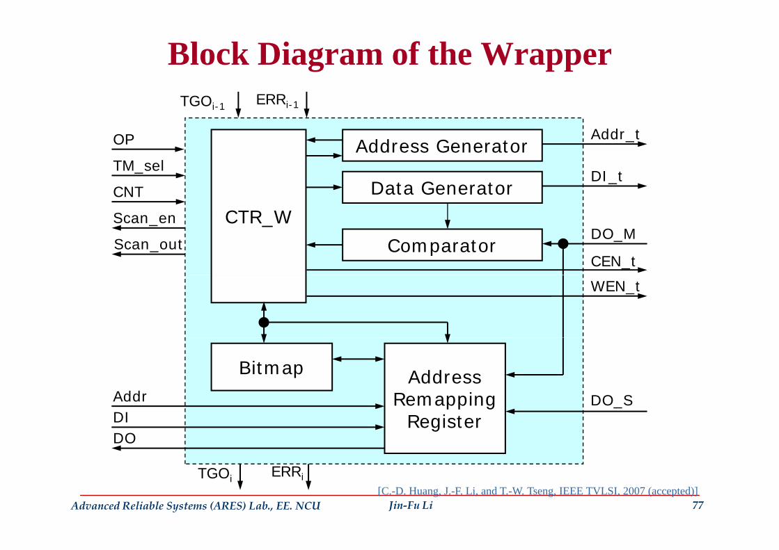
Block Diagram of the Wrapper
Address GeneratorOP Addr_t
ERRi-1TGOi-1
CTR W
Address Generator
Data GeneratorTM_sel
CNT
S
DI_t
CTR_WComparator
Scan_en
Scan_outDO_M
CEN_t
WEN_t
AddressRemapping
BitmapAddr DO SRemapping
RegisterAddrDIDO
DO_S
Advanced Reliable Systems (ARES) Lab., EE. NCU Jin-Fu Li 77
ERRiTGOi[C.-D. Huang, J.-F. Li, and T.-W. Tseng, IEEE TVLSI, 2007 (accepted)]

Area Cost of the WrapperArea overhead of the Wrapper is defined as the ratio of the area of the wrapper to the area of the corresponding memoryExperimental results for an 8Kx64-bit memory p y
Redundancy Configuration Wrapper Area Area Overhead
2R2C 6739 gates 2.3%
2R3C 7342 gates 2.5%
3R3C 8317 gates 2.8%
Area cost of Wrappers for different memory sizesMemory Configuration Wrapper Area Area Overhead
8K x 16 3944 gates 4.6%
4K x 32 4825 gates 5.8%
2K 64 6501 7 1%
Advanced Reliable Systems (ARES) Lab., EE. NCU Jin-Fu Li 78
2K x 64 6501 gates 7.1%
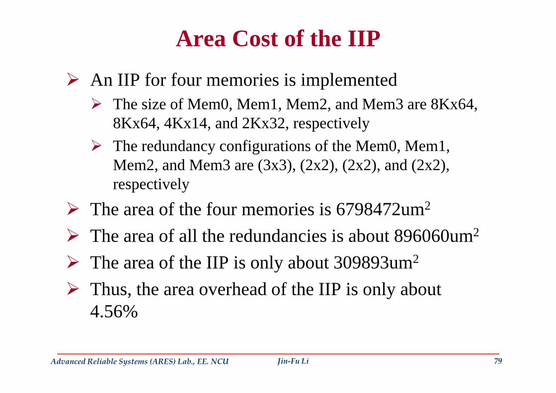
Area Cost of the IIP
An IIP for four memories is implementedThe size of Mem0 Mem1 Mem2 and Mem3 are 8Kx64The size of Mem0, Mem1, Mem2, and Mem3 are 8Kx64, 8Kx64, 4Kx14, and 2Kx32, respectivelyThe redundancy configurations of the Mem0, Mem1, y g , ,Mem2, and Mem3 are (3x3), (2x2), (2x2), and (2x2), respectively
The area of the four memories is 6798472um2
The area of all the redundancies is about 896060um2The area of all the redundancies is about 896060umThe area of the IIP is only about 309893um2
Th th h d f th IIP i l b tThus, the area overhead of the IIP is only about 4.56%
Advanced Reliable Systems (ARES) Lab., EE. NCU Jin-Fu Li 79
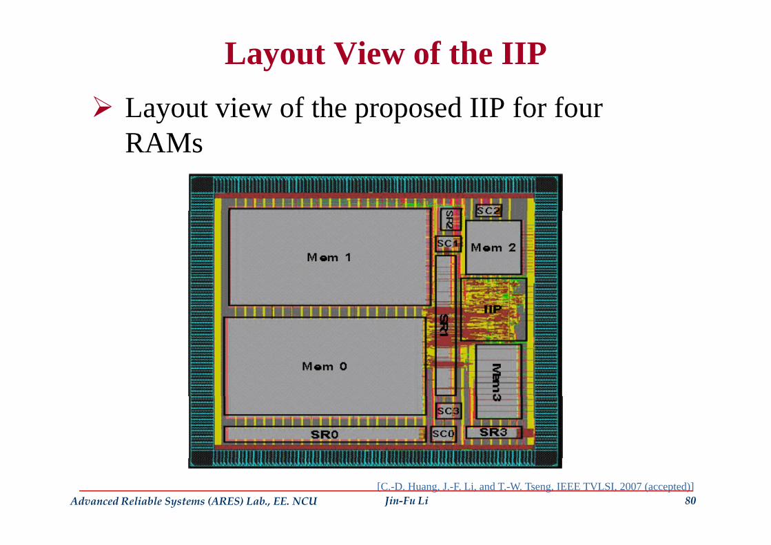
Layout View of the IIPLayout view of the proposed IIP for four RAMsRAMs
Advanced Reliable Systems (ARES) Lab., EE. NCU Jin-Fu Li 80[C.-D. Huang, J.-F. Li, and T.-W. Tseng, IEEE TVLSI, 2007 (accepted)]

Conclusions
Embedded memories represent more and more f t hi (SOC) d iarea of system-on-chip (SOC) designs
The yield of memory cores dominates the yield of chips
Various BIRA techniques have been presentedVarious BIRA techniques have been presentedDifferent BISR techniques for memories in SOCs h b t dhave been presented
Advanced Reliable Systems (ARES) Lab., EE. NCU Jin-Fu Li 81

References 1. T. Kawagoe, J. Ohtani, M. Niiro, T. Ooishi, M. Hamada, and H. Hidaka, “A built-in self-repair analyzer
(CRESTA) for embedded DRAMs,” in Proc. Int’l Test Conf. (ITC), 2000, pp. 567.574.2. V. Schober, S. Paul, and O. Picot, “Memory built-in self-repair using redundant words,” in Proc. Int’l
Test Conf. (ITC), Baltimore, Oct. 2001, pp. 995-1001.3. Y. Zorian, “Embedded memory test & repair: Infrastructure IP for SOC yield,” in Proc. Int’l Test Conf.
(ITC), Baltmore, Oct. 2002, pp. 340.349.4. C.-T. Huang, C.-F. Wu, J.-F. Li and C.-W. Wu,”Built-in redundancy analysis for memory yield
improvement,” IEEE Trans. Reliability, vol. 52, no. 4, pp. 386-399, Dec. 2003. 5. J.-F. Li, J.-C. Yeh, R.-F. Huang, C.-W. Wu, P.-Y. Tsai, A. Hsu, and E. Chow,”A built-in self-repair
scheme for semiconductor memories with 2-D redundancies,” in Proc. IEEE Int. Test Conf. (ITC),(Charlotte), pp. 393-402, Sept. 2003.
6. J.-F. Li, J.-C. Yeh, R.-F. Huang, and C.-W. Wu,”A built-in self-repair design for RAMs with 2-D d d i l lredundancies,” IEEE Trans. Very Large Scale Integration Systems, vol.13, no.6, pp. 742-745, June, 2005.
7. S.-K. Lu, Y.-C. Tsai, C.-H. Hsu, K.-H. Wang, and C.-W. Wu, “Efficient built-in redundancy analysis for embedded memories with 2-D redundancy,” IEEE Trans. on VLSI Systems, vol. 14, no. 1, pp. 34–42, Jan. 2006.
8 T W T J F Li C C H A P K Chi d E Ch "A fi bl b il i lf i8. T.-W. Tseng, J.-F. Li, C.-C. Hsu, A. Pao, K. Chiu, and E. Chen, "A reconfigurable built-in self-repair scheme for multiple self-repairable RAMs in SOCs," in Proc. IEEE Int. Test Conf. (ITC), (Santa Clara), Paper 30.2, pp. 1-8, Oct. 2006.
9. C.-D. Huang, J.-F. Li, and T.-W. Tseng,”ProTaR: an infrastructure IP for repairing RAMs in SOCs,” IEEE Trans Very Large Scale Integration Systems vol 15 no 10 pp 1135 1143 Oct 2007IEEE Trans. Very Large Scale Integration Systems, vol.15, no.10, pp. 1135-1143, Oct. 2007.
10. R.-F. Huang, J.-F. Li, J.-C. Yeh, and C.-W. Wu,”RAISIN: a tool for evaluating redundancy analysis schemes in repairable embedded memories,” IEEE Design and Test of Computers, vol.24, no.4, pp. 386-396, July-August 2007.
Advanced Reliable Systems (ARES) Lab., EE. NCU Jin-Fu Li 82
Related Documents