Electronics and Communication Engineering VHDL and VERILOG Lab Manual VI Semester – JU INDEX 1. HDL Prerequisites 2. Syllabus 3. Procedure & Requirements – Conduction of Programs (H/W, S/W) 4. VHDL & Verilog codes with pattern generator & logic analyzer results 5. Interfacing Experiments 6. About Pattern generator & Logic analyzer 7. Pin details of interfacing boards 8. Pin details of mother board 9. VIVA questions Page 1 of 152

Welcome message from author
This document is posted to help you gain knowledge. Please leave a comment to let me know what you think about it! Share it to your friends and learn new things together.
Transcript
Electronics and Communication EngineeringVHDL and VERILOG Lab Manual
VI Semester – JU
INDEX
1.HDL Prerequisites2.Syllabus3.Procedure & Requirements – Conduction of
Programs (H/W, S/W)4.VHDL & Verilog codes with pattern generator &
logic analyzer results5.Interfacing Experiments6.About Pattern generator & Logic analyzer7.Pin details of interfacing boards8.Pin details of mother board9.VIVA questions
HDL Prerequisites
Page 1 of 132
PLI
Programming Language Interface (PLI) of Verilog HDL is a mechanism to interface Verilog programs with programs written in C language. It also provides mechanism to access internal databases of the simulator from the C program.
C or C++ or JAVA is mandatory if the program is required to access a DB
PLI is used for implementing system calls which would have been hard to do otherwise (or impossible) using Verilog syntax. Or, in other words, you can take advantage of both the paradigms - parallel and hardware related features of Verilog and sequential flow of C - using PLI
Some of the most common applications of PLI are delay back annotation, writing delay calculators and developing user interface
VHDL does not have a PLI (one more reason for you to switch to Verilog), although preliminary proposals are there for standardizing such an interface.
VHDL
VHDL (VHSIC hardware description language) is a hardware description language used in electronic design automation to describe digital and mixed-signal systems such as field-programmable gate arrays and integrated circuits.
A simulation program is used to test the logic design using simulation models to represent the logic circuits that interface to the design. This collection of simulation models is commonly called a testbench.
The key advantage of VHDL, when used for systems design, is that it allows the behavior of the required system to be described (modeled) and verified (simulated) before synthesis tools translate the design into real hardware (gates and wires).
Another benefit is that VHDL allows the description of a concurrent system. VHDL is a dataflow language , unlike procedural computing languages such as BASIC, C, and assembly code, which all run sequentially, one instruction at a time.
VHDL project is multipurpose. Being created once, a calculation block can be used in many other projects. However, many formational and functional block parameters can be tuned (capacity parameters,
Page 2 of 132
memory size, element base, block composition and interconnection structure).
VHDL project is portable. Being created for one element base, a computing device project can be ported on another element base, for example VLSI with various technologies.
There are four versions of VHDL. The original release of the VHDL language occured in 1987 with the adoption of the Language Reference Manual as an IEEE standard. In 1993, the IEEE-1076 standard was modified and ratified and became known as VHDL'93. This is now widely supported. In 2000, the VHDL 1076 2000 Edition appeared - this fixed shared variables by introducing the idea of protected types. Finally, VHDL 1076-2002 appeared. This includes protected mode types, but also changes ports of mode buffer to make them more usable, along with some other small changes. In practise, VHDL 1076-1993 is the current flavour of VHDL which is widely supported by tool vendors.
There is an activity to develop an improved VHDL, and VHDL-2008 was released in January 2009.
Compilation: Multiple design-units (entity/architecture pairs), that reside in the same system file, may be separately compiled if so desired. However, it is good design practice to keep each design unit in it's own system file in which case separate compilation should not be an issue.
Design Reusability: Procedures and functions may be placed in a package so that they are available to any design-unit that wishes to use them.
High Level Constructs: There are more constructs and features for high-level modeling in VHDL than there are in Verilog: package statements for model reuse, configuration statements for configuring design structure, generic statements for generic models that can be individually characterized, for example, bit width.
Low Level Constructs: Simple two input logical operators are built into the language, they are: NOT, AND, OR, NAND, NOR, XOR and XNOR. Any timing must be separately specified using the after clause. Separate constructs defined under the VITAL language must be used to define the cell primitives of ASIC and FPGA libraries.
Language Extensions: Has an attribute called 'foreign that allows architectures and subprograms to be modeled in another language.
Managing large designs: Configuration, generate, generic and package statements all help manage large design structures.
IEEE standard libraries in VHDL are :
a)std_logic_1164.b) numeric_std.c) numeric_bit .
Page 3 of 132
d) std_logic_arith .e) std_logic_unsigned .
Objects of VHDL are :
a) Signalb) Variablec) Constant
Signals - Signals are like wires which connect design entities together and communicate changes in values within a design.
In VHDL, there is no unary reduction operator. But, a loop statement can be used in VHDL to perform the same operation as a Verilog unary reduction operator. Delays in VHDL – Inertial, Propagation, Delta (default) & Transport
delays
Differences between signal & variable are :
Signals connect design entities together. Signals can be declared both inside and out side of the process. It has three properties like type & type attributes, Value, Time. Signals assign its value after delta delay. Signals require more memory. Variable These are the identifiers within process or subprograms. This can only be declared within process can't be used outside a process. It has only two properties like Type,Value. Variable assigned its value immediately. Variable require less memory.
Statements inside a process execute sequentially. Examples of such sequential statements are- if, else, elsif, case, loops, wait (on/until/for)
Including a package in the program
library work;use work.pkg_name.all;Add these lines in code just after the standard library declaration.
Page 4 of 132
An entity can have multiple architectures. To select one of the many architecture bodies that an entity may have, CONFIGURATION is used.
Setup time is the time required for the synchronous inputs of a flip-flop to be stable before a clock pulse is applied. Hold time is the time that the synchronous inputs of a flip-flop remain stable after the active clock transaction is finished.
Metastability is an unknown state. It is neither 0 or nor 1. If the setup time and hold time are violated, the flip-flop goes into metastability state. Metastability can be overcome by using faster flip flops and proper synchronizers.
Attribute is a value, function, range, signal, type or constant that can be associated with certain names within VHDL description. These names could be among others, entity name, architecture name.
Test bench is a code that generates the stimuli to test out design correctness. It automatically verifies the code accuracy. It also verifies whether the code meets the circuit requirements.
A buffer is an OUT port with read capability. A buffer port may have at most one driver within the architecture where as inout port is just bidirectional port.
Severity levels in assertion are Warning , Error (default) , Failure.
RTL
In integrated circuit design, register-transfer level (RTL) is a level of abstraction used in describing the operation of a synchronous digital circuit. In RTL design, a circuit's behavior is defined in terms of the flow of signals (or transfer of data) between hardware registers, and the logical operations performed on those signals
Page 5 of 132
RTL focuses on describing the flow of signals between registers.
RTL is used in the logic design phase of the integrated circuit design cycle.
An RTL description is usually converted to a gate-level description of the circuit by a logic synthesis tool. The synthesis results are then used by placement and routing tools to create a physical layout.
Differences between algorithmic model and RTL model: RTL model has few additional inputs & outputs over and above that of the algorithmic models. They are inputs Clock, Reset_N and Load, and the output Done.
Verilog
Similar to C Compilation: Care must be taken with both the compilation order of
code written in a single file and the compilation order of multiple files. Simulation results can change by simply changing the order of compilation.
Design Reusability: There is no concept of packages in Verilog. Functions and procedures used within a model must be defined in the module. To make functions and procedures generally accessible from different module statements the functions and procedures must be placed in a separate system file and included using the `include compiler directive.
High level constructs: Except for being able to parameterize models by overloading parameter constants, there is no equivalent to the high-level VHDL modeling statements in Verilog.
Low Level Constructs: The Verilog language was originally developed with gate level modeling in mind, and so has very good constructs for modeling at this level and for modeling the cell primitives of ASIC and FPGA libraries. Examples include User Defined Primitive s (UDP), truth tables and the specify block for specifying timing delays across a module.
Language Extensions: The Programming Language Interface (PLI) is an interface mechanism between Verilog models and Verilog software tools. For example, a designer, or more likely, a Verilog tool vendor, can specify user defined tasks or functions in the C programming language, and then call them from the Verilog source description. Use of such tasks or functions make a Verilog model nonstandard and so
Page 6 of 132
may not be usable by other Verilog tools. Their use is not recommended.
Managing large designs: There are no statements in Verilog that help manage large designs.
ADVENT :1. Verilog 95 - Cadence transferred Verilog into the public domain
under the Open Verilog International (OVI) (now known as Accellera) organization. Verilog was later submitted to IEEE and became IEEE Standard 1364-1995, commonly referred to as Verilog-95.
2. Verilog 2001 - adds explicit support for (2's complement) signed nets and variables, built-in operators: +, -, /, *, >>>, can instantiate an array of instances, File I/O has been improved by several new system-tasks,
3. Verilog 2005 - consists of minor corrections, spec clarifications, and a few new language features (such as the uwire keyword)
4. Verilog AMS - attempts to integrate analog and mixed signal modeling with traditional Verilog
5. SystemVerilog - with many new features and capabilities to aid design-verification and design-modeling. As of 2009, the SystemVerilog and Verilog language standards were merged into SystemVerilog 2009 (IEEE Standard 1800-2009).
System Verilog
Is a combined Hardware Description Language and Hardware Verification Language based on extensions to Verilog.
Provides enhanced hardware-modeling features, which improve the RTL design productivity and simplify the design process.
SystemVerilog is an integrated part of the Simulation tool. There is no need for any external tool, GUI or interface (such as PLI) in order to run it. There is no need for any new compilation commands.
Advantages of SystemVerilog Vs. other Verification Languages
SystemVerilog has several key advantages that involve standardization,
performance and adoption by engineers.
Page 7 of 132
• SystemVerilog was adopted as a standard by the Accellera organization,
and is currently in the process of final approval by IEEE. This ensures a wide
embracing and supported by multiple vendors of EDA tools and verification
IP's, as well as interoperability between different tools and vendors.
• Since SystemVerilog is an extension of the popular Verilog language, the
adoption process of SystemVerilog by engineers is extremely easy and
straightforward. SystemVerilog enables engineers to adopt a modular
approach for integrating new modules into any existing code. As a result, the
risks and costs of adopting a new verification language are reduced.
• Being an integrated part of the simulation engine, eliminates the need for
external verification tools and interfaces, and thus ensures optimal
performance (running at least x2 faster than with any other verification
languages).
What is the SystemVerilog’s contribution to the RTL design?
SystemVerilog brings a higher level of abstraction to the Verilog designer.
Constructs and commands like Interfaces, new Data types (logic, int),
Enumerated types, Arrays, Hardware-specific always (always_ff,
always_comb) and others allow modeling of RTL designs easily, and with less
coding.
SystemVerilog also extends the modeling aspects of Verilog by adding a
Direct Programming Interface which allows C, C++, SystemC and Verilog
code to work together without the overhead of the Verilog PLI.
TESTBENCH
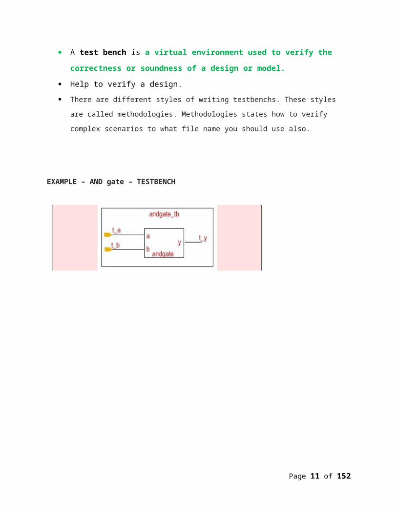
A test bench is a virtual environment used to verify the
correctness or soundness of a design or model.
Help to verify a design.
Page 8 of 132
There are different styles of writing testbenchs. These styles are called methodologies.
Methodologies states how to verify complex scenarios to what file name you should use also.
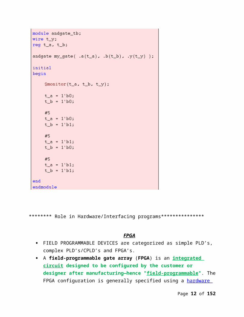
EXAMPLE – AND gate – TESTBENCH
Page 9 of 132
******** Role in Hardware/Interfacing programs***************
FPGA FIELD PROGRAMMABLE DEVICES are categorized as simple PLD’s,
complex PLD’s/CPLD’s and FPGA’s. A field-programmable gate array (FPGA) is an integrated circuit
designed to be configured by the customer or designer after manufacturing—hence "field-programmable". The FPGA configuration is generally specified using a hardware description language (HDL), similar to that used for an application-specific
Page 10 of 132
integrated circuit (ASIC) (circuit diagrams were previously used to specify the configuration.
FPGAs contain programmable logic components called "logic blocks", and a hierarchy of reconfigurable interconnects that allow the blocks to be "wired together"—somewhat like many (changeable) logic gates that can be inter-wired in (many) different configurations.
Differences between CPLD and FPGA
Density of macro cells & number of gates in a FPGA is comparatively larger.
CPLD is flash memory based for configuration. It could run after power-up.FPGA is SRAM memory based for configuration. It should be configured every time after power-up. It needs external configuration memory.
FPGAs are very sensitive on power supply glitches and have complicated architecture.
FPGAs are very good solution for complex logic prototyping e.g. FIFOs, CACHE memories, dual port SRAM, CPU cores and SOCs.
For less complex high speed designs like memory mapping in an address bus, use CPLDs. These are cheaper due to their simpler architecture.
The most important thing is when there has no supply, program in FPGA will disappear, but program will still locate in cpld even there has no supply.
Summary:
1. FPGA contains up to 100,000 of tiny logic blocks while CPLD contains only a few blocks of logic that reaches up to a few thousands.
2. In terms of architecture, FPGAs are considered as ‘fine-grain’ devices while CPLDs are ‘coarse-grain’.
3. FPGAs are great for more complex applications while CPLDs are better for simpler ones.
4. FPGAs are made up of tiny logic blocks while CPLDs are made of larger blocks.
Page 11 of 132
5. FPGA is a SRAM-based digital logic chip while CPLD is EEPROM-based/Flash memory.
6. Normally, FPGAs are more expensive while CPLDs are much cheaper.
7. Delays are much more predictable in CPLDs than in FPGAs.
Synthesis
Synthesis is the stage in the design flow which is concerned with translating your VHDL code into gates - and that's putting it very simply! First of all, the VHDL must be written in a particular way for the target technology that you are using. Of course, a synthesis tool doesn't actually produce gates - it will output a net list of the design that you have synthesized that represents the chip which can be fabricated through an ASIC or FPGA vendor
Logic Analyzers
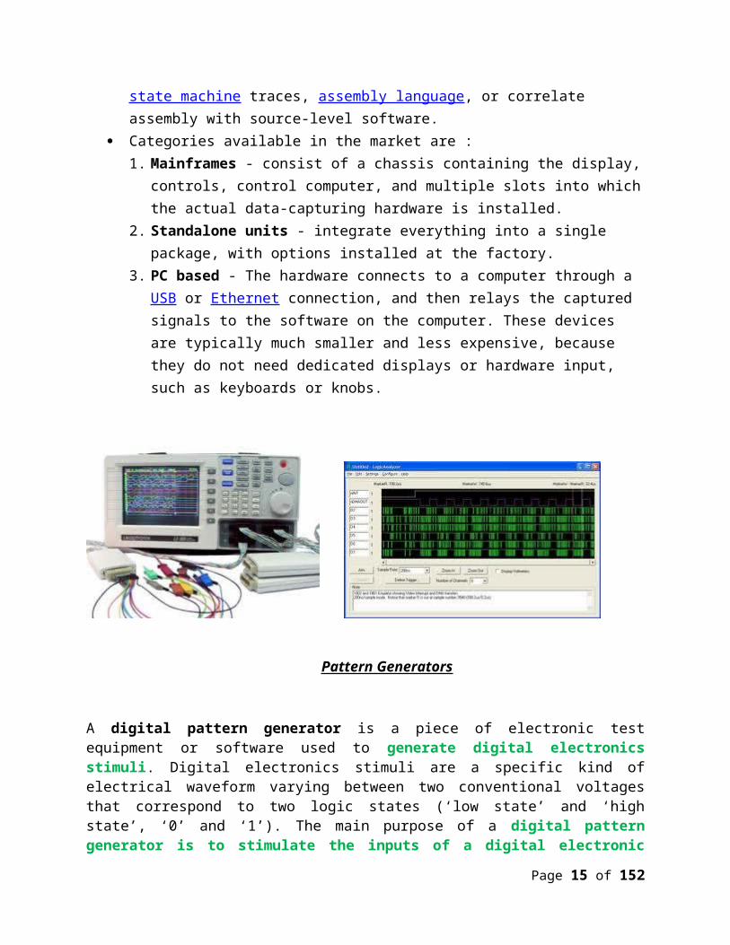
A logic analyzer is an electronic instrument which displays signals in a digital circuit. A logic analyzer may convert the captured data into timing diagrams, protocol decodes, state machine traces, assembly language, or correlate assembly with source-level software.
Categories available in the market are :1. Mainframes - consist of a chassis containing the display, controls,
control computer, and multiple slots into which the actual data-capturing hardware is installed.
2. Standalone units - integrate everything into a single package, with options installed at the factory.
3. PC based - The hardware connects to a computer through a USB or Ethernet connection, and then relays the captured signals to the software on the computer. These devices are typically much smaller and less expensive, because they do not need dedicated displays or hardware input, such as keyboards or knobs.
Page 12 of 132
Pattern Generators
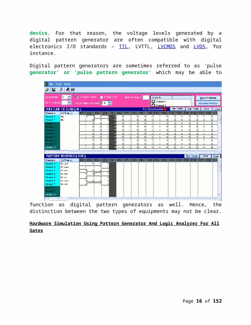
A digital pattern generator is a piece of electronic test equipment or software used to generate digital electronics stimuli. Digital electronics stimuli are a specific kind of electrical waveform varying between two conventional voltages that correspond to two logic states (‘low state’ and ‘high state’, ‘0’ and ‘1’). The main purpose of a digital pattern generator is to stimulate the inputs of a digital electronic device. For that reason, the voltage levels generated by a digital pattern generator are often compatible with digital electronics I/O standards – TTL, LVTTL, LVCMOS and LVDS, for instance.
Digital pattern generators are sometimes referred to as ‘pulse generator’ or ‘pulse pattern generator’ which may be able to function as digital pattern generators as well. Hence, the distinction between the two types of equipments may not be clear.
Page 13 of 132
Hardware Simulation Using Pattern Generator And Logic Analyzer For All Gates
Digital IC Design
Page 14 of 132
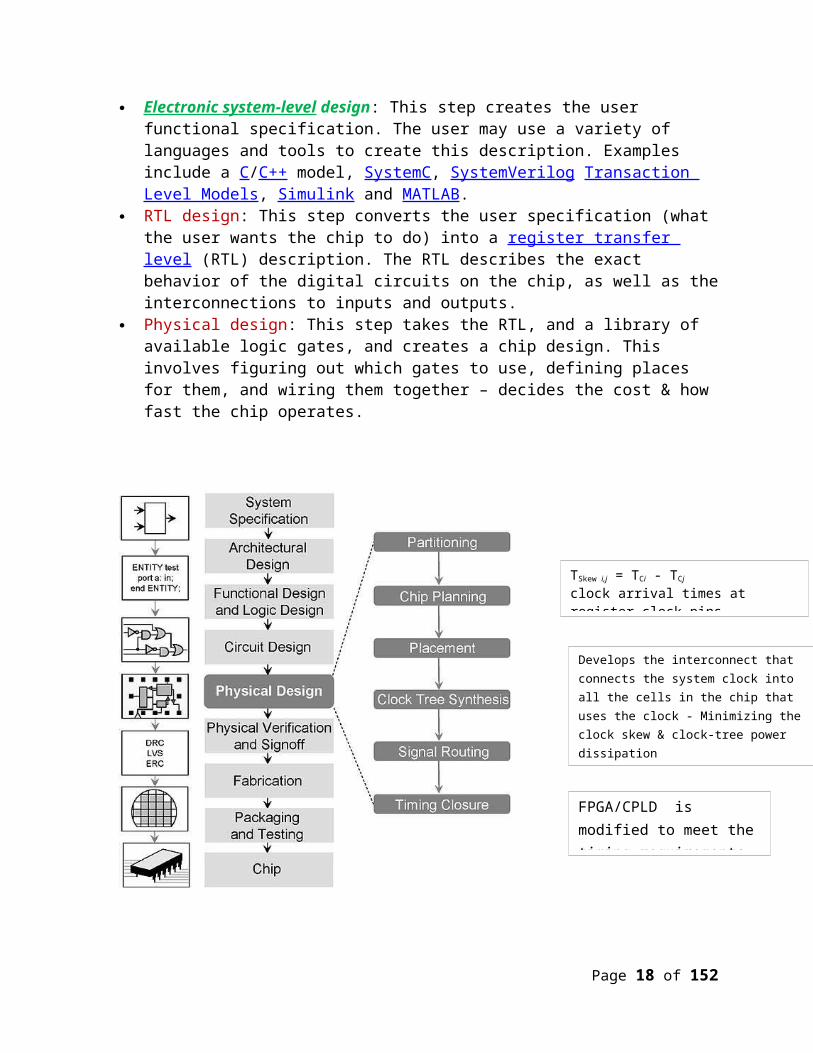
Roughly speaking, digital IC design can be divided into three parts.
Electronic system-level design: This step creates the user functional specification. The user may use a variety of languages and tools to create this description. Examples include a C/C++ model, SystemC, SystemVerilog Transaction Level Models, Simulink and MATLAB.
RTL design: This step converts the user specification (what the user wants the chip to do) into a register transfer level (RTL) description. The RTL describes the exact behavior of the digital circuits on the chip, as well as the interconnections to inputs and outputs.
Physical design: This step takes the RTL, and a library of available logic gates, and creates a chip design. This involves figuring out which gates to use, defining places for them, and wiring them together – decides the cost & how fast the chip operates.
Page 15 of 132
FPGA/CPLD is modified to meet the timing requirements
Develops the interconnect that connects the system clock into all the cells in the chip that uses the clock - Minimizing the clock skew & clock-tree power dissipation
TSkew i,j = TCi - TCj
clock arrival times at register clock pins
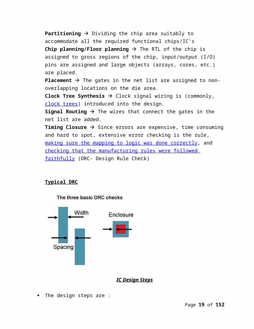
Partitioning Dividing the chip area suitably to accommodate all the required functional chips/IC’sChip planning/Floor planning The RTL of the chip is assigned to gross regions of the chip, input/output (I/O) pins are assigned and large objects (arrays, cores, etc.) are placed.Placement The gates in the net list are assigned to non-overlapping locations on the die area.Clock Tree Synthesis Clock signal wiring is (commonly, clock trees) introduced into the design.Signal Routing The wires that connect the gates in the net list are added.Timing Closure Since errors are expensive, time consuming and hard to spot, extensive error checking is the rule, making sure the mapping to logic was done correctly, and checking that the manufacturing rules were followed faithfully (DRC- Design Rule Check)
Typical DRC
IC Design Steps
The design steps are :1. Feasibility study and die size estimate2. Functional Verification3. Circuit/RTL design4. Circuit/RTL simulation Logic simulation5. Floor planning 6. Design review7. Layout
Page 16 of 132
8. Layout verification9. Static timing analysis 10. Layout review11. Design For Test and Automatic test pattern generation12. Design for manufacturability (IC) 13. Mask data preparation 14. Wafer fabrication 15. Die test 16. Packaging 17. Post silicon validation&integration 18. Device characterization19. Tweak (if necessary)20. Datasheet generation Portable Document Format21. Ramp up22. Production23. Yield Analysis / Warranty Analysis Reliability (semiconductor)24. Failure analysis on any returns25. Plan for next generation chip using production information if
possible.
TOOLS
Altera VHDL simulatorXilinx (used in the lab) – Downloadable components available, easy to download to FPGACadence SpecmanSynopsys VeraModelsim Mentor Graphics
SYLLABUS
PROGRAMMING (using VHDL and Verilog)
Page 17 of 132
1. Write HDL code to realize all the logic gates.2. Write a HDL program for the following combinational designs :
A. 2 to 4 decoderB. 8 to 3 (encoder without priority & with priority)C. 8 to 1 multiplexerD. 4 bit binary to gray converterE. Multiplexer, de-multiplexer, comparator.
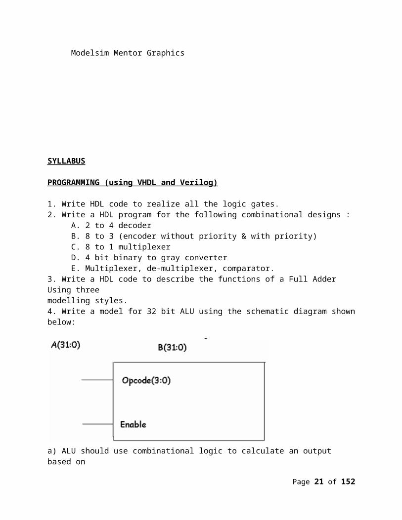
3. Write a HDL code to describe the functions of a Full Adder Using threemodelling styles.4. Write a model for 32 bit ALU using the schematic diagram shown below:
a) ALU should use combinational logic to calculate an output based onthe four bit op-code input.b) ALU should pass the result to the out bus when enable line in highand tri-state the out bus when the enable line is low.c) ALU should decode the 4 bit op-code according to the given inexample below :OPCODE ALU OPERATION
1. A + B2. A – B3. A Complement4. A * B5. A AND B6. A OR B7. A NAND B8. A XOR B
5. Develop the HDL code for the following flip-flops - SR, D, JK & T.6. Design 4 bit binary, BCD counters (Synchronous reset andAsynchronous reset) and “any sequence” counters.INTERFACING
1. Write HDL code to display messages on the given seven segmentdisplay and LCD and accepting Hex key pad input data.
Page 18 of 132
2. Write HDL code to control speed, direction of DC and Stepper motor.3. Write HDL code to accept 8 channel Analog signal, Temperaturesensors and display the data on LCD panel or Seven segment display.4. Write HDL code to generate different waveforms (Sine, Square,Triangle, Ramp etc.,) using DAC change the frequency and amplitude.5. Write HDL code to simulate Elevator operations6. Write HDL code to control external lights using relays.
Requirements:
1. VHDL software with both front-end and backend (Design entry,synthesis, simulation, implementation and programming.2. FPGA kit with minimum 400,000 gate density3. Bit pattern generator/Logic analyzer4. Interfacing cards like LCD,7-segment display, keyboard, ADC, DAC,Stepper Motor, DC Motor & Relays.
Procedure:
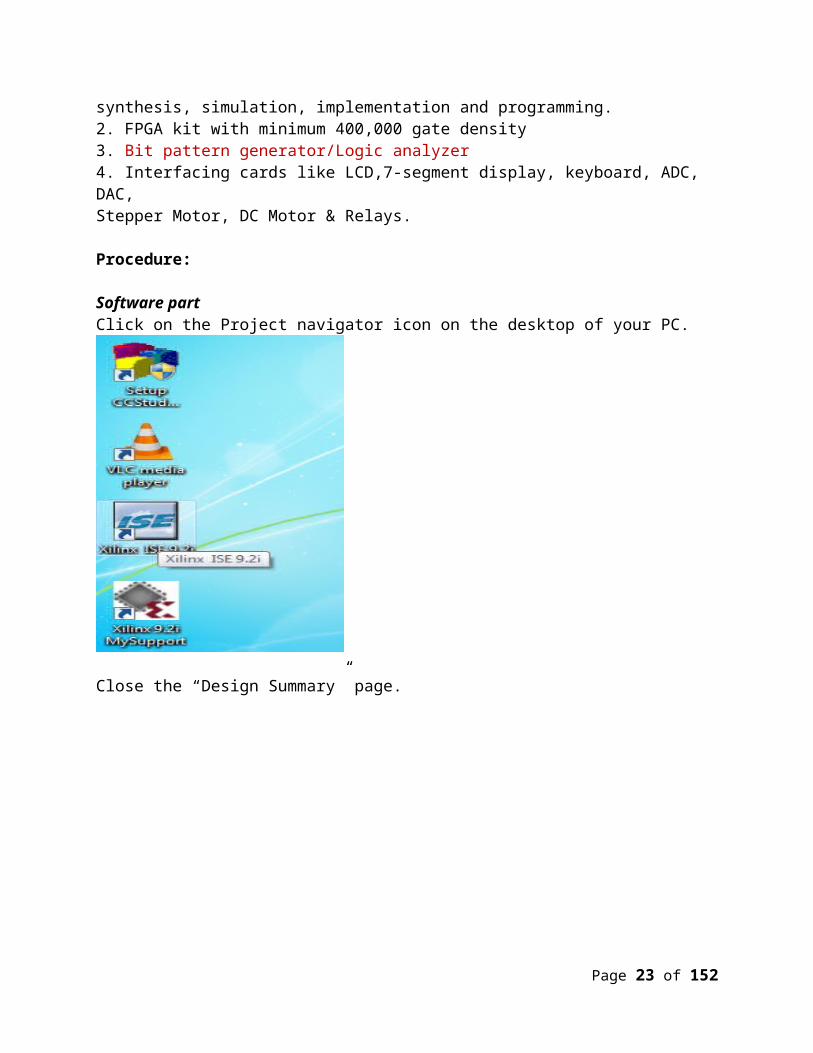
Software partClick on the Project navigator icon on the desktop of your PC.
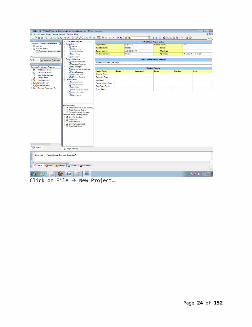
Close the “Design Summary” page.
Page 19 of 132
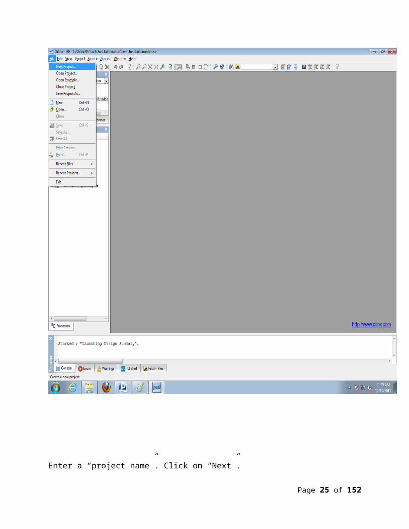
Click on File New Project…
Page 20 of 132
Enter a “project name”. Click on “Next”.
Page 21 of 132
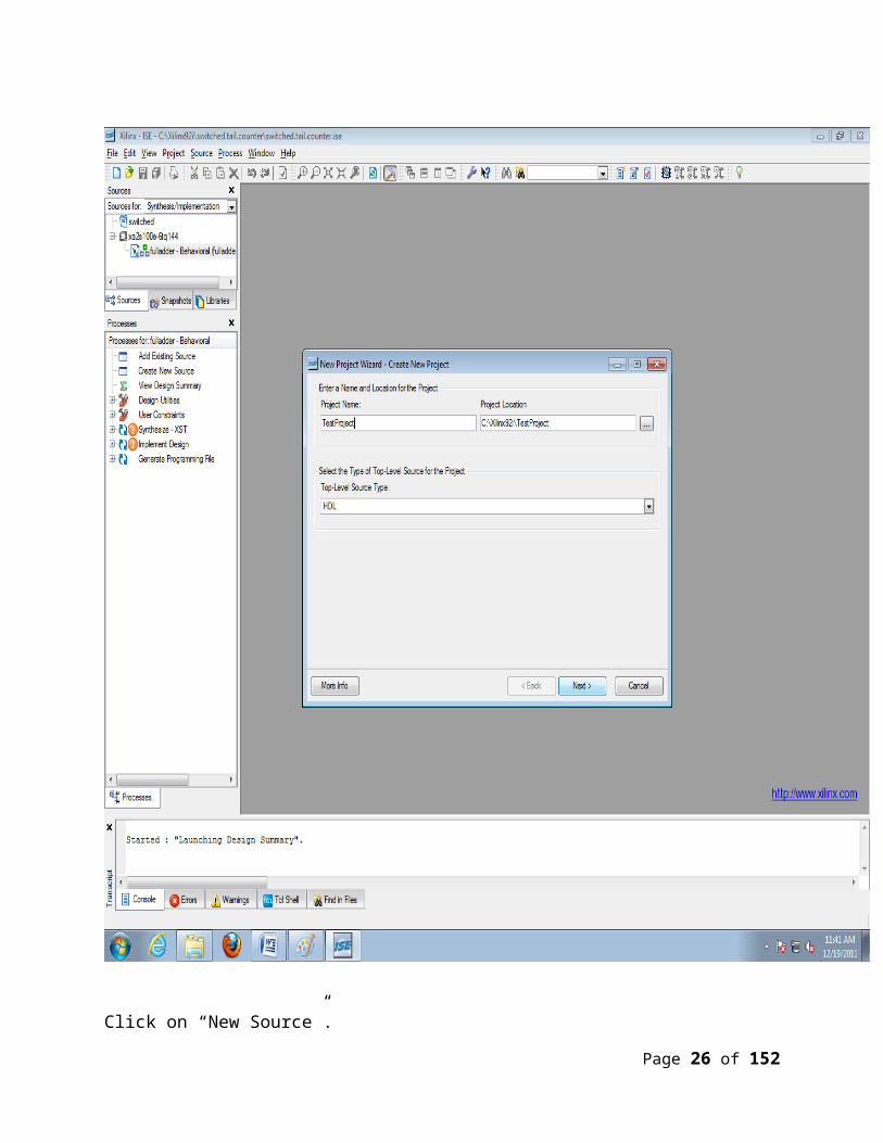
Click on “New Source”.
Page 22 of 132
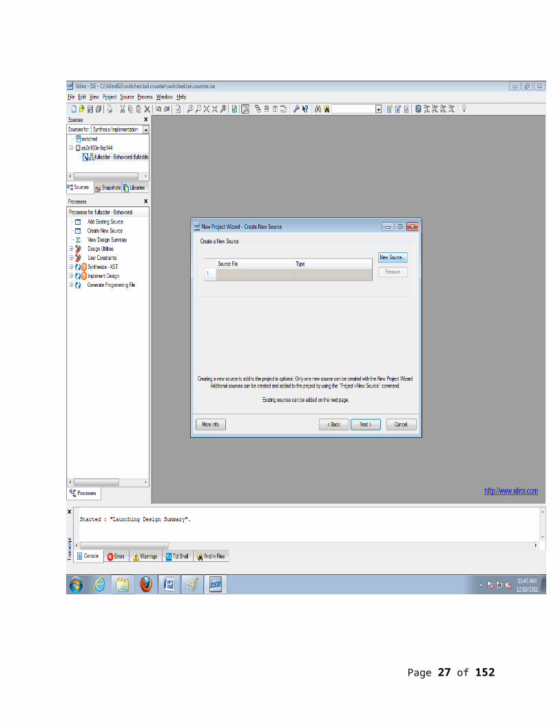
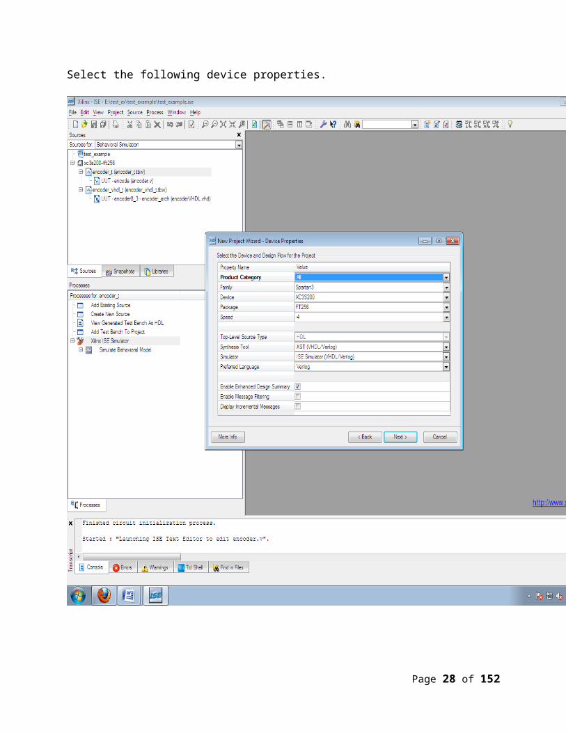
Select the following device properties.
Page 23 of 132
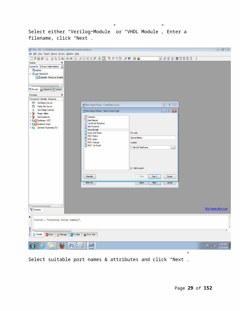
Select either “Verilog Module” or “VHDL Module”, Enter a filename, click “Next”.
Page 24 of 132
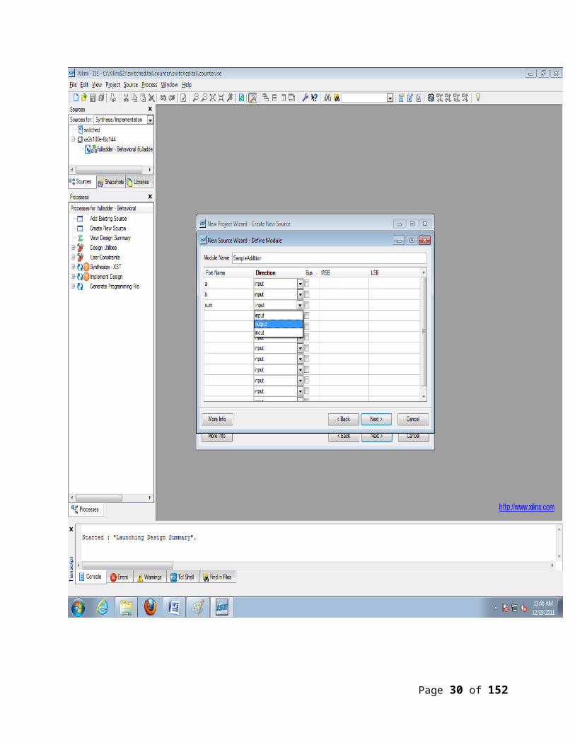
Select suitable port names & attributes and click “Next”.
Page 25 of 132
Page 26 of 132
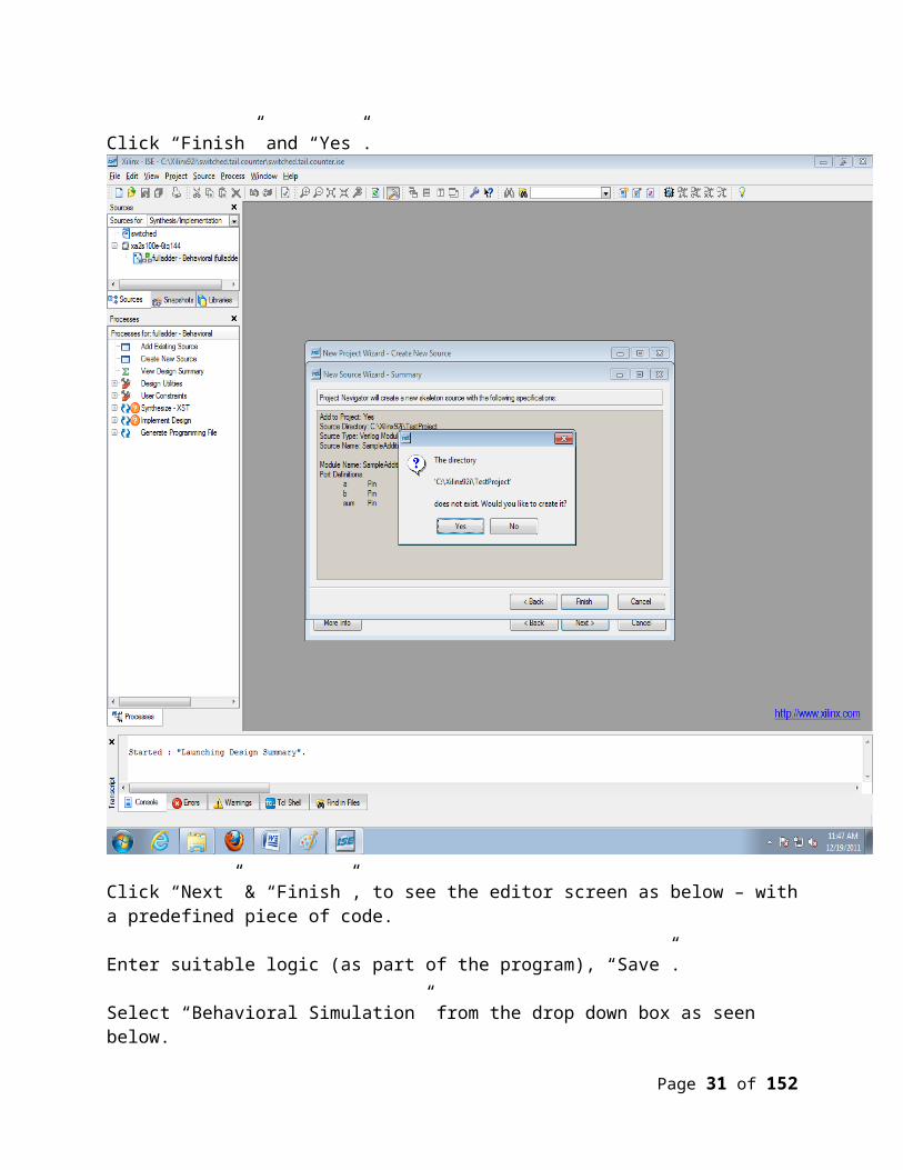
Click “Finish” and “Yes”.
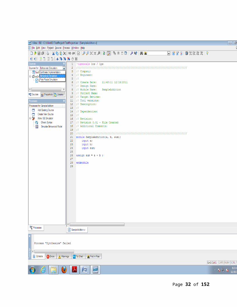
Click “Next” & “Finish”, to see the editor screen as below – with a predefined piece of code.
Enter suitable logic (as part of the program), “Save”.
Select “Behavioral Simulation” from the drop down box as seen below.
Page 27 of 132
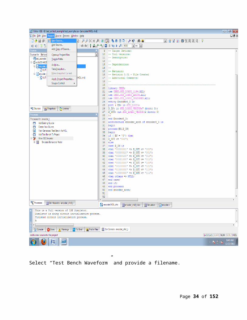
Double click on “Processes Check Syntax”, for compiler errors.
Page 28 of 132
Follow the same procedure that was followed while creating a Verilog Module. But, now add a new source to the existing project application.
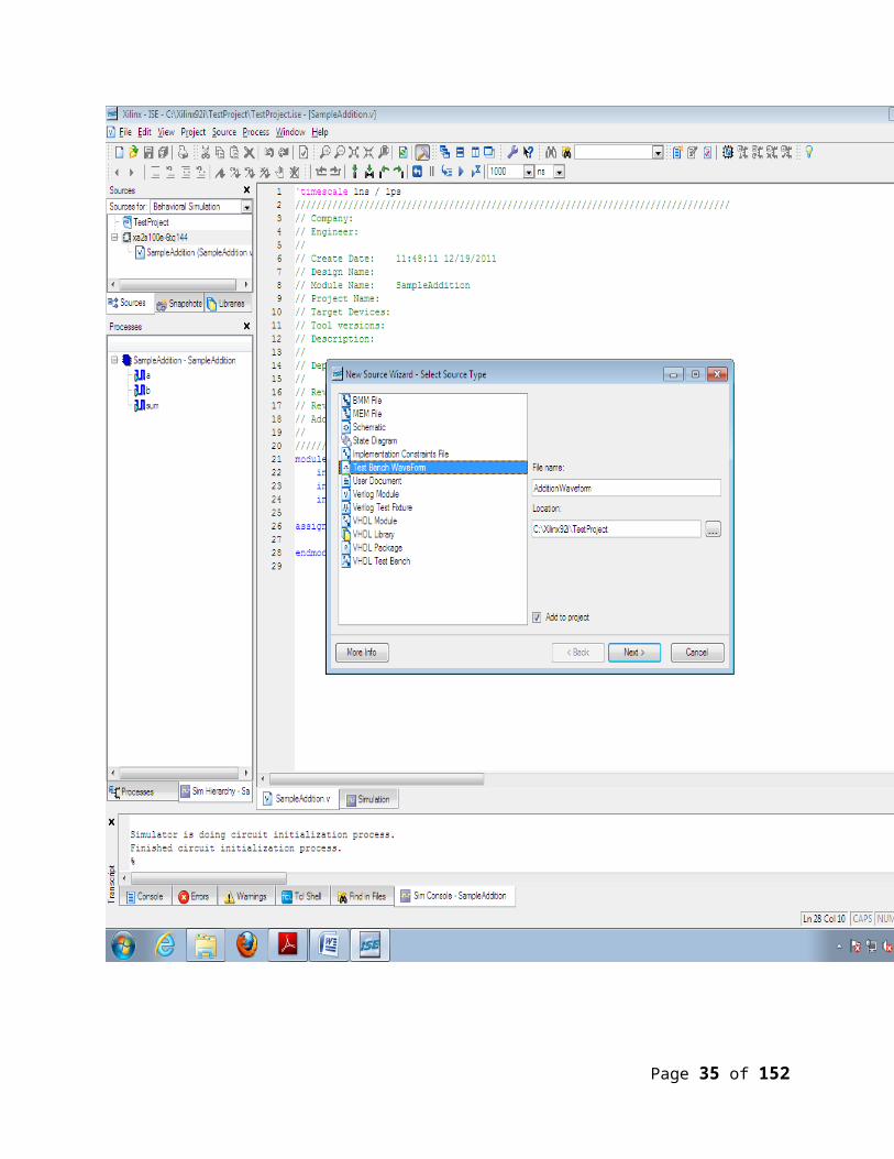
Select “Test Bench Waveform” and provide a filename.
Page 29 of 132
Page 30 of 132
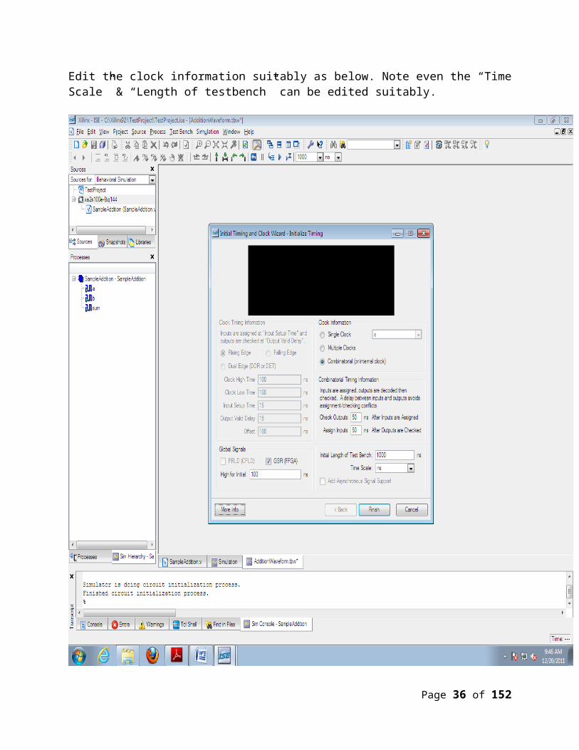
Edit the clock information suitably as below. Note even the “Time Scale” & “Length of testbench” can be edited suitably.
Page 31 of 132
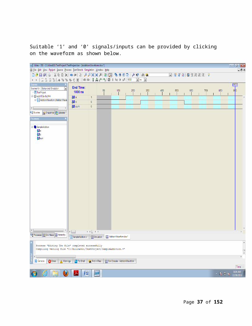
Suitable ‘1’ and ‘0’ signals/inputs can be provided by clicking on the waveform as shown below.
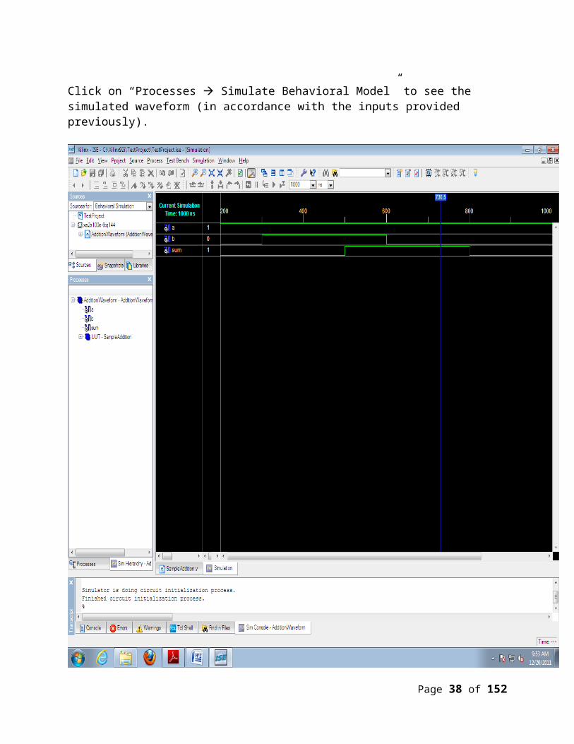
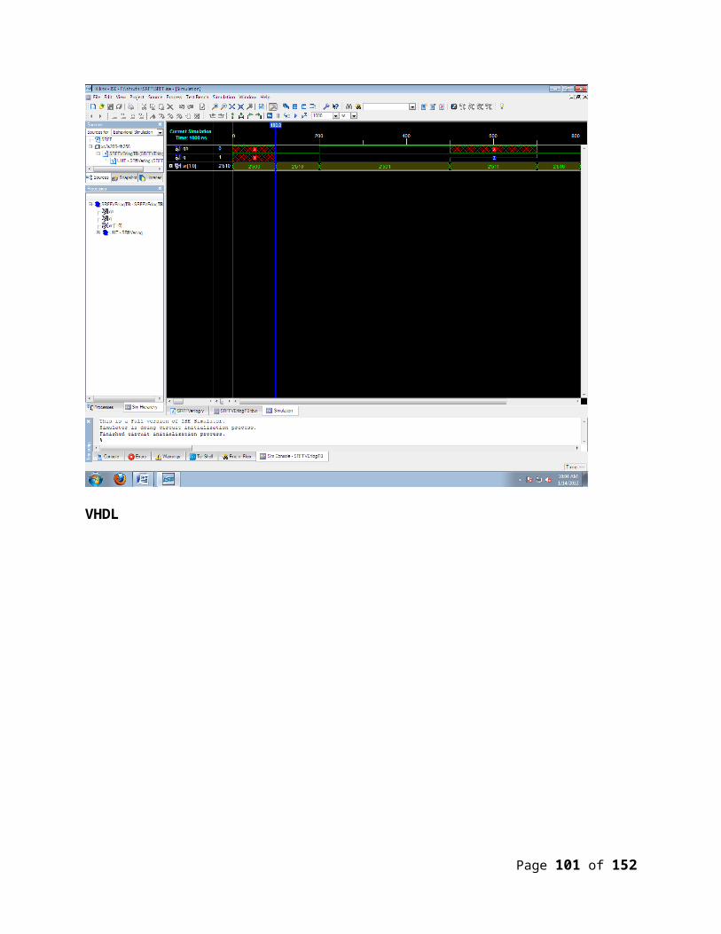
Click on “Processes Simulate Behavioral Model” to see the simulated waveform (in accordance with the inputs provided previously).
Page 32 of 132
Hardware part
Page 33 of 132
PROCEDURE
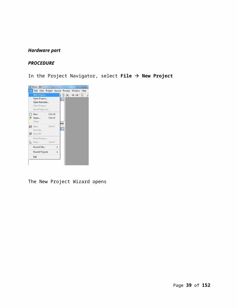
In the Project Navigator, select File New Project
The New Project Wizard opens
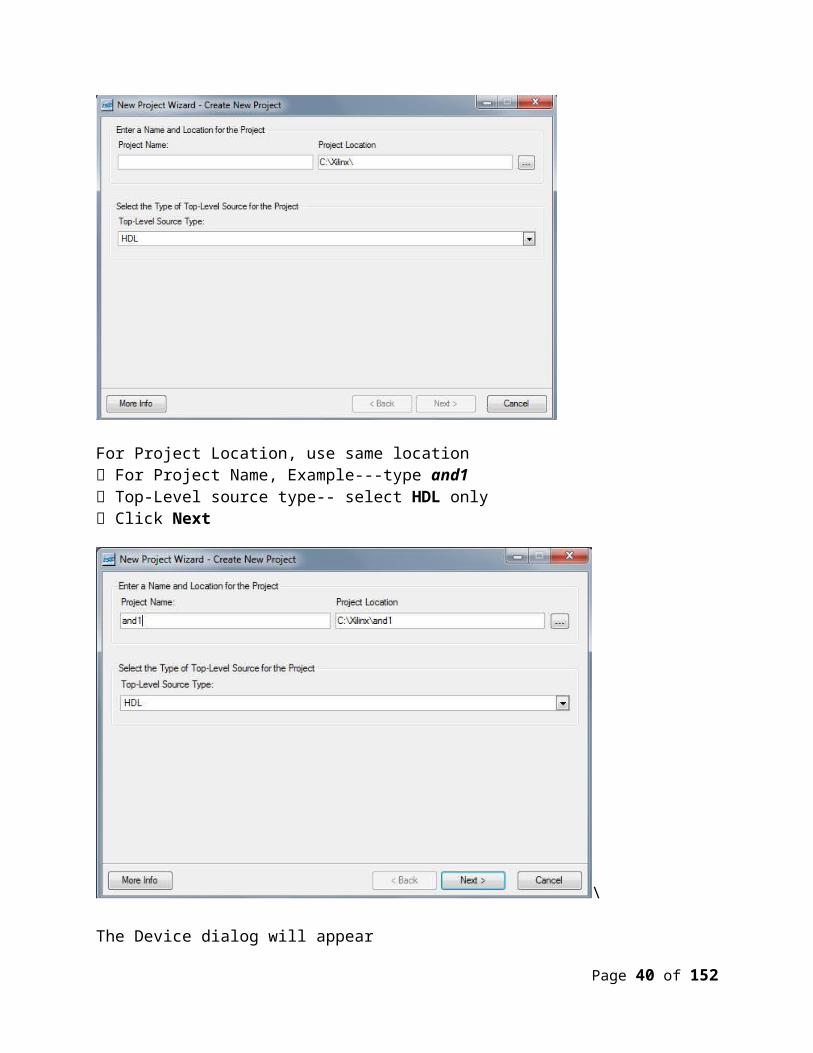
For Project Location, use same location For Project Name, Example---type and1 Top-Level source type-- select HDL only Click Next
Page 34 of 132
\
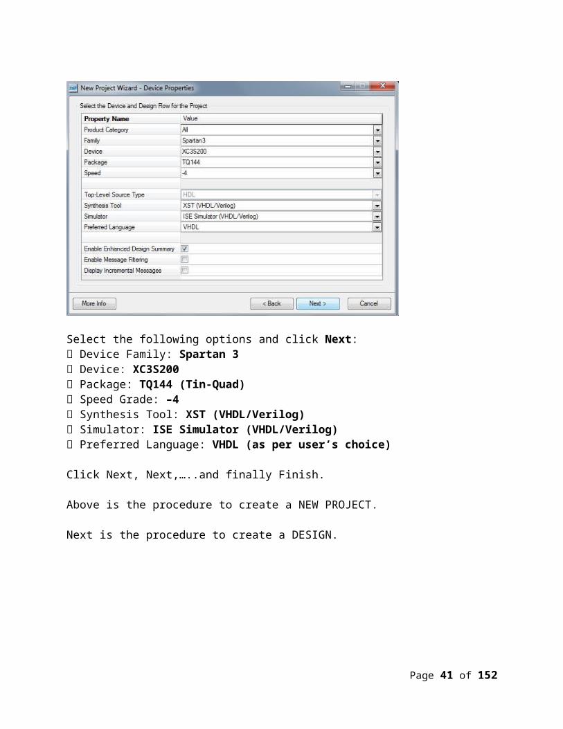
The Device dialog will appear
Select the following options and click Next: Device Family: Spartan 3 Device: XC3S200 Package: TQ144 (Tin-Quad)
Page 35 of 132
Speed Grade: –4 Synthesis Tool: XST (VHDL/Verilog) Simulator: ISE Simulator (VHDL/Verilog) Preferred Language: VHDL (as per user’s choice)
Click Next, Next,…..and finally Finish.
Above is the procedure to create a NEW PROJECT.
Next is the procedure to create a DESIGN.
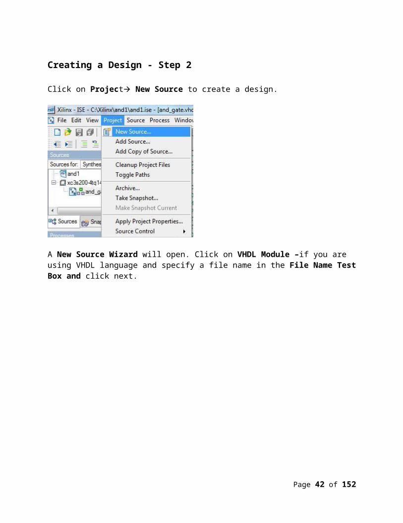
Creating a Design - Step 2
Click on Project New Source to create a design.
A New Source Wizard will open. Click on VHDL Module –if you are using VHDL language and specify a file name in the File Name Test Box and click next.
Page 36 of 132
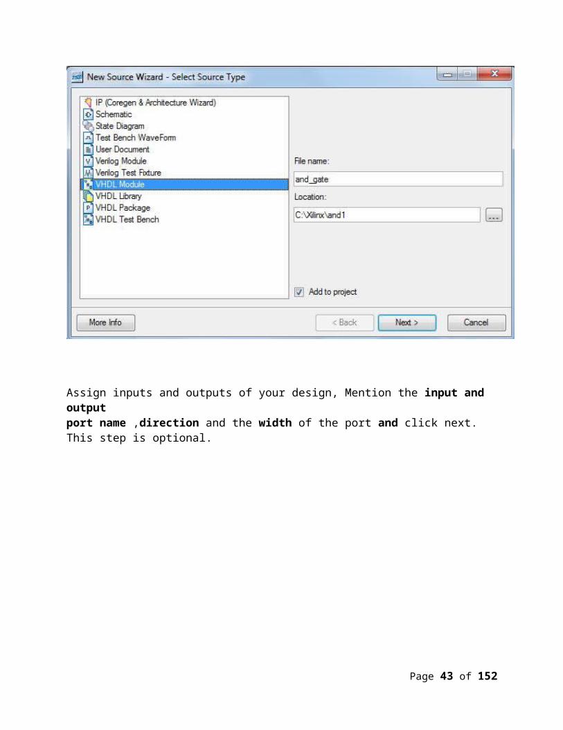
Assign inputs and outputs of your design, Mention the input and output port name ,direction and the width of the port and click next. This step is optional.
Page 37 of 132
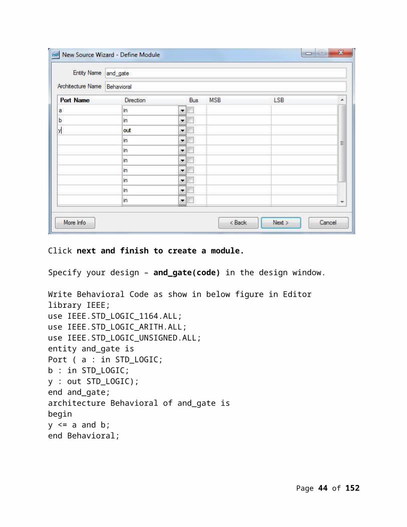
Click next and finish to create a module.
Specify your design – and_gate(code) in the design window.
Write Behavioral Code as show in below figure in Editorlibrary IEEE;use IEEE.STD_LOGIC_1164.ALL;use IEEE.STD_LOGIC_ARITH.ALL;use IEEE.STD_LOGIC_UNSIGNED.ALL;entity and_gate isPort ( a : in STD_LOGIC;b : in STD_LOGIC;y : out STD_LOGIC);end and_gate;architecture Behavioral of and_gate isbeginy <= a and b;end Behavioral;
Page 38 of 132
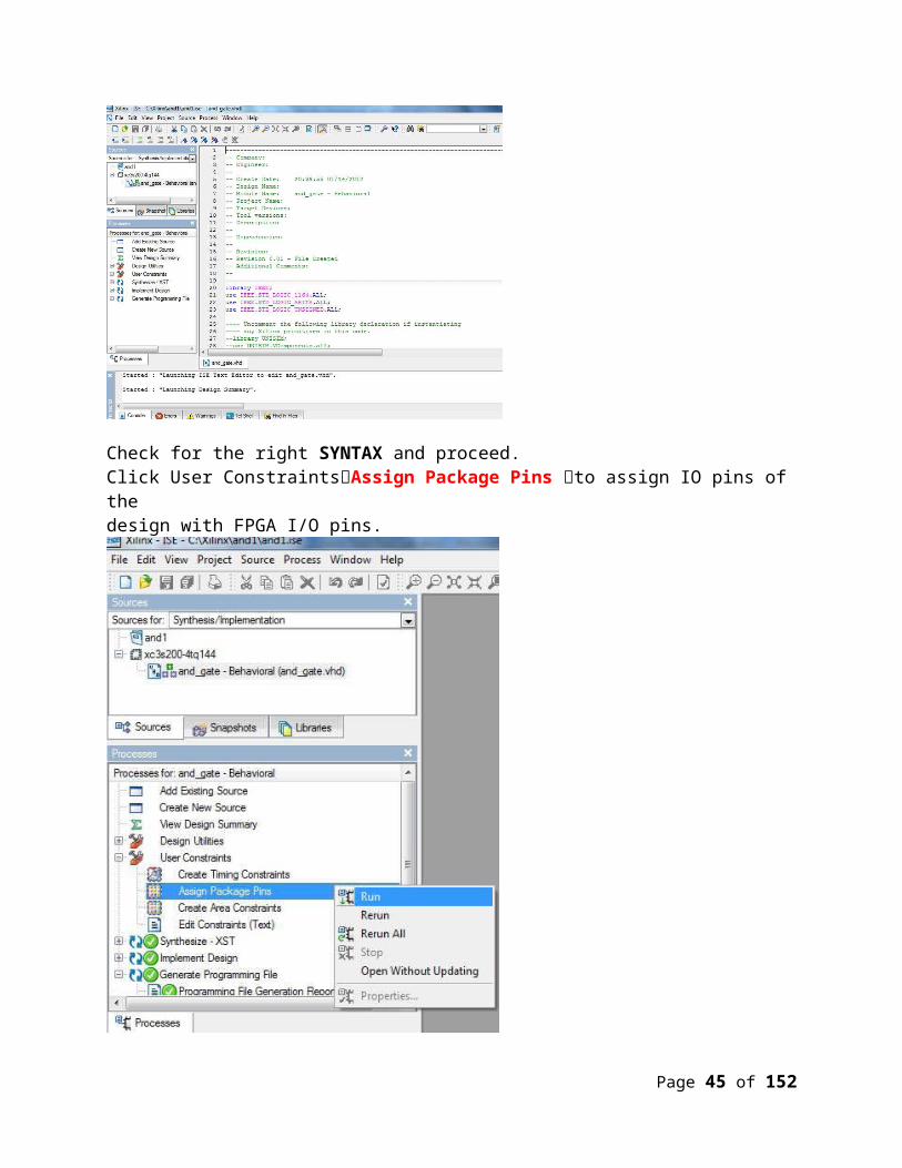
Check for the right SYNTAX and proceed.Click User ConstraintsAssign Package Pins to assign IO pins of thedesign with FPGA I/O pins.
Page 39 of 132
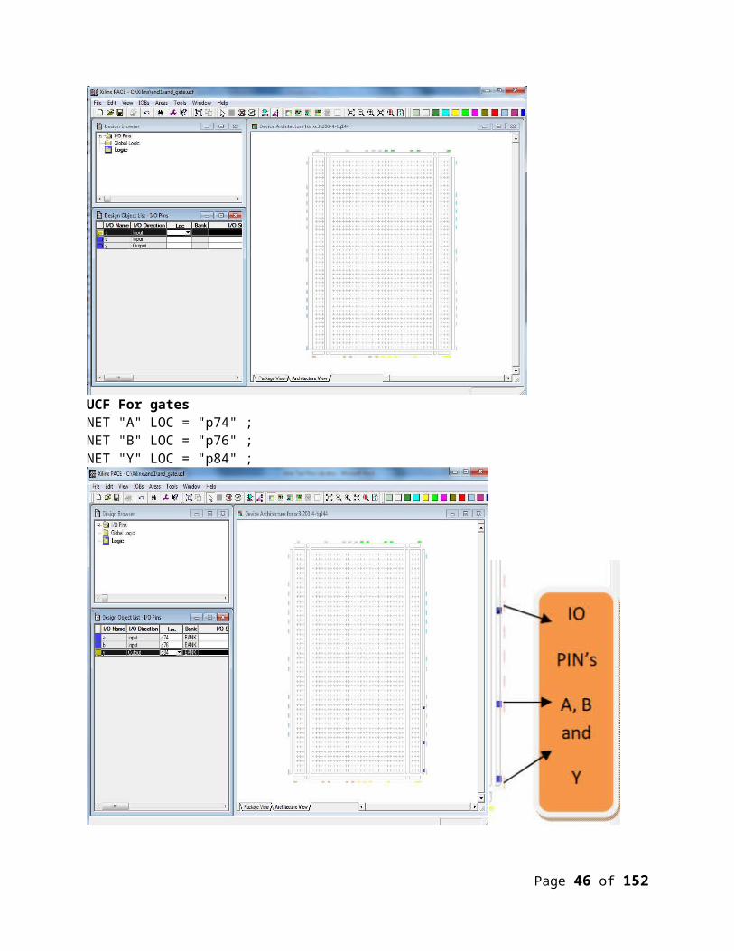
UCF For gatesNET "A" LOC = "p74" ;NET "B" LOC = "p76" ;NET "Y" LOC = "p84" ;
Page 40 of 132
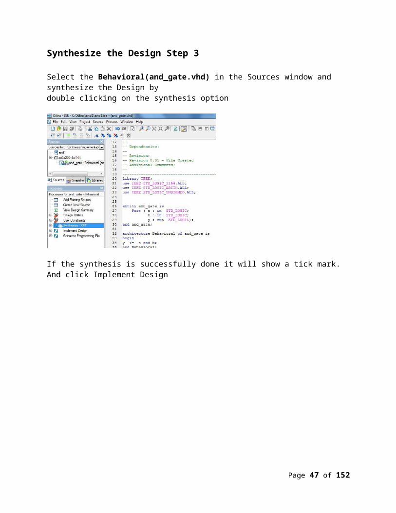
Synthesize the Design Step 3
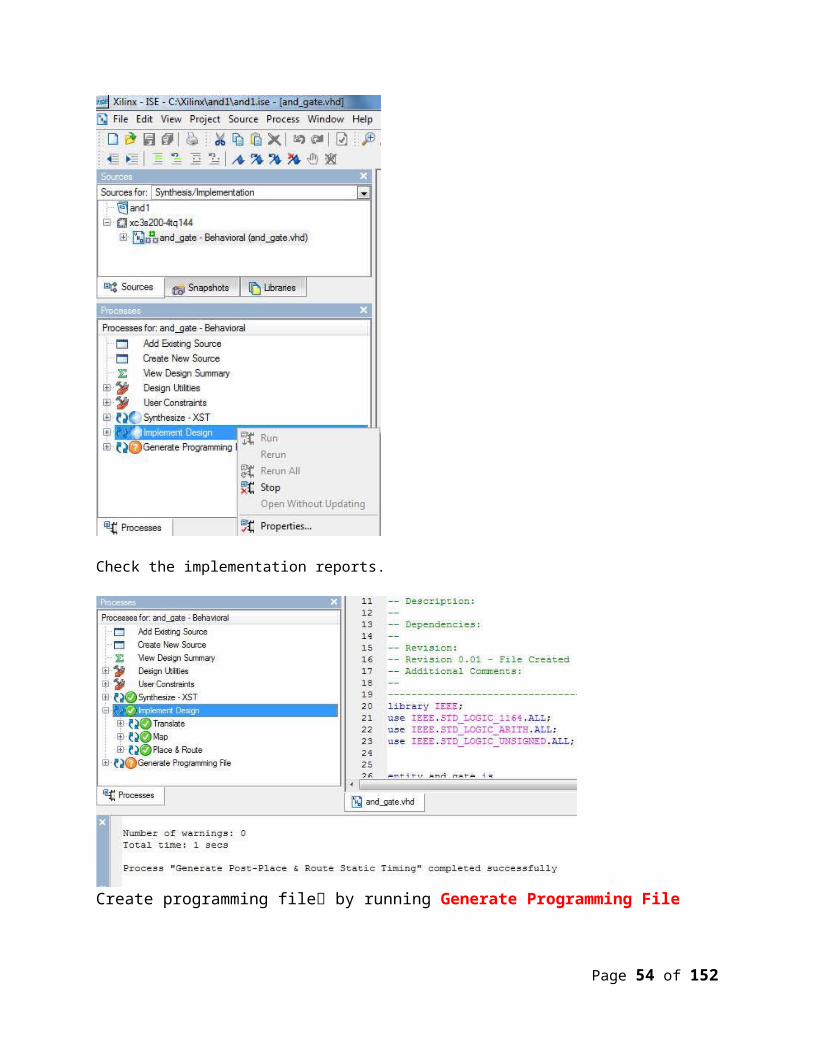
Select the Behavioral(and_gate.vhd) in the Sources window and synthesize the Design bydouble clicking on the synthesis option
If the synthesis is successfully done it will show a tick mark. And click Implement Design
Page 41 of 132
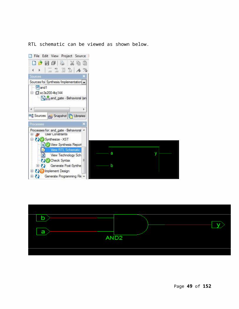
RTL schematic can be viewed as shown below.
Page 42 of 132
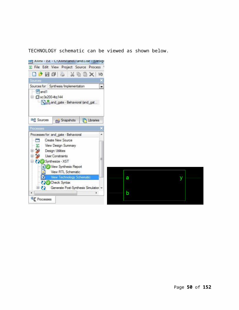
TECHNOLOGY schematic can be viewed as shown below.
Page 43 of 132
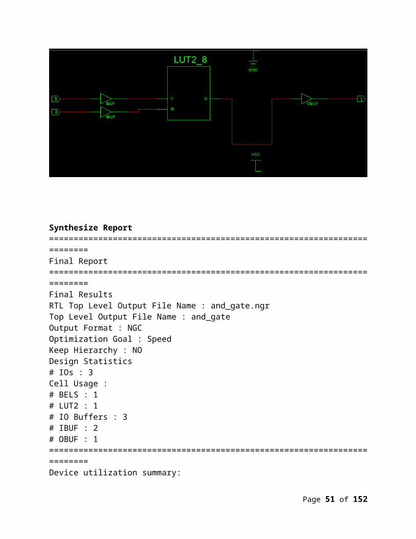
Synthesize Report
Page 44 of 132
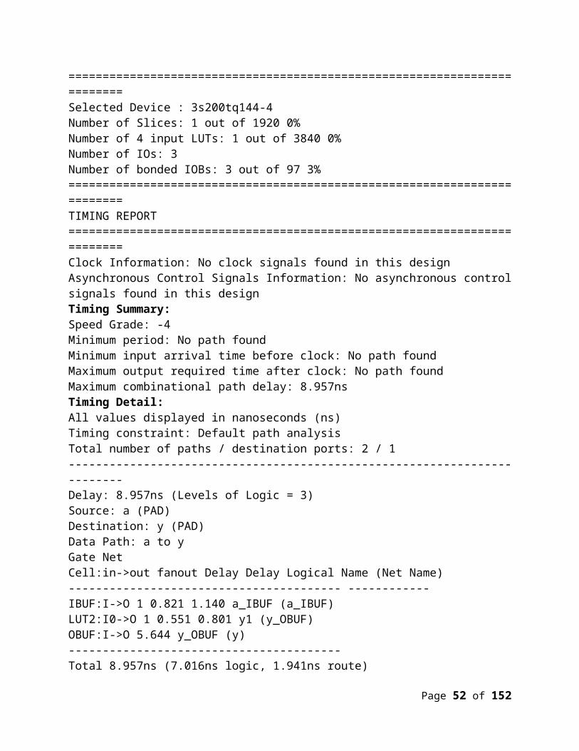
=========================================================================Final Report=========================================================================Final ResultsRTL Top Level Output File Name : and_gate.ngrTop Level Output File Name : and_gateOutput Format : NGCOptimization Goal : SpeedKeep Hierarchy : NODesign Statistics# IOs : 3Cell Usage :# BELS : 1# LUT2 : 1# IO Buffers : 3# IBUF : 2# OBUF : 1=========================================================================Device utilization summary:=========================================================================Selected Device : 3s200tq144-4Number of Slices: 1 out of 1920 0%Number of 4 input LUTs: 1 out of 3840 0%Number of IOs: 3Number of bonded IOBs: 3 out of 97 3%=========================================================================TIMING REPORT=========================================================================Clock Information: No clock signals found in this designAsynchronous Control Signals Information: No asynchronous control signals found in this designTiming Summary:Speed Grade: -4Minimum period: No path foundMinimum input arrival time before clock: No path foundMaximum output required time after clock: No path foundMaximum combinational path delay: 8.957nsTiming Detail:All values displayed in nanoseconds (ns)Timing constraint: Default path analysis
Page 45 of 132
Total number of paths / destination ports: 2 / 1-------------------------------------------------------------------------Delay: 8.957ns (Levels of Logic = 3)Source: a (PAD)Destination: y (PAD)Data Path: a to yGate NetCell:in->out fanout Delay Delay Logical Name (Net Name)---------------------------------------- ------------IBUF:I->O 1 0.821 1.140 a_IBUF (a_IBUF)LUT2:I0->O 1 0.551 0.801 y1 (y_OBUF)OBUF:I->O 5.644 y_OBUF (y)----------------------------------------Total 8.957ns (7.016ns logic, 1.941ns route)(78.3% logic, 21.7% route)=========================================================================CPU : 3.82 / 4.05 s | Elapsed : 4.00 / 4.00 s
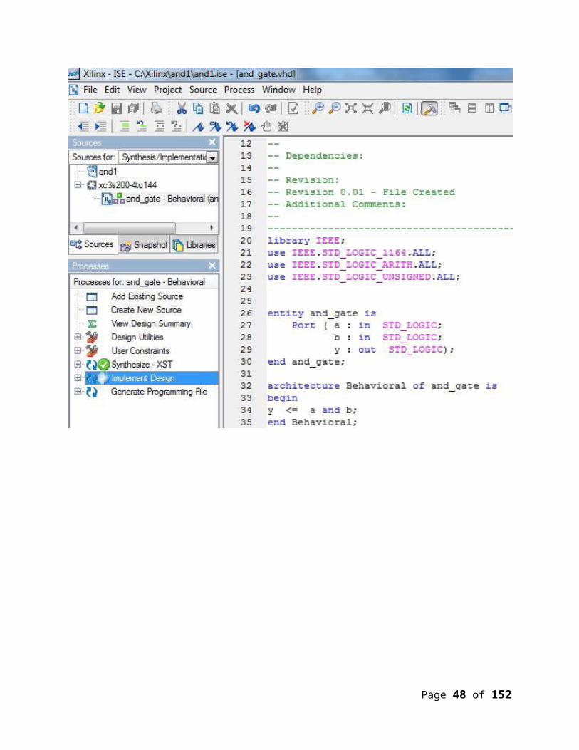
Implement the design by double clicking on the implementation toolselection Implement Design
Page 46 of 132
Check the implementation reports.
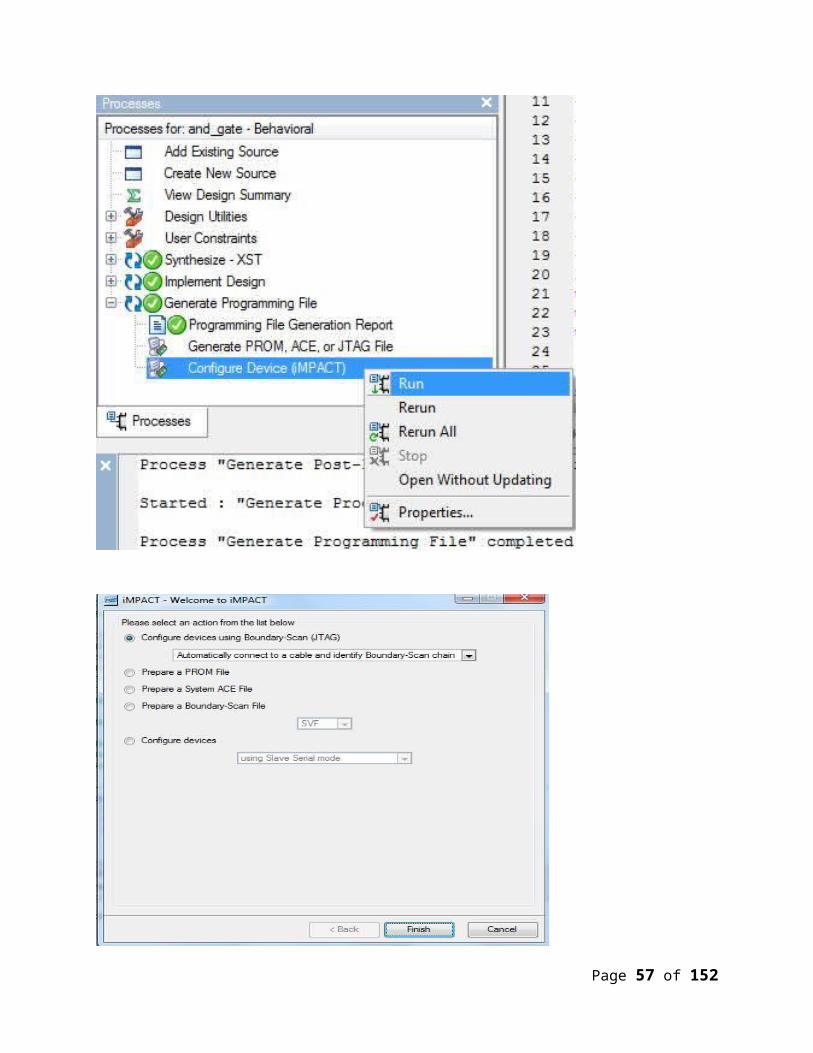
Create programming file by running Generate Programming File
Page 47 of 132
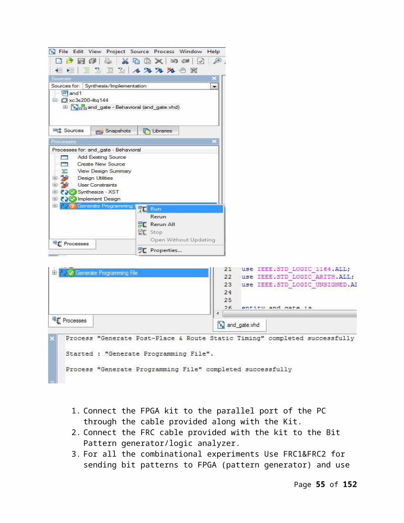
1. Connect the FPGA kit to the parallel port of the PC through the cable provided along with the Kit.
2. Connect the FRC cable provided with the kit to the Bit Pattern generator/logic analyzer.
3. For all the combinational experiments Use FRC1&FRC2 for sending bit patterns to FPGA (pattern generator) and use FRC3 &FRC4 for receiving the logic from FPGA (logic Analysis).
Page 48 of 132
4. For all sequential circuits Use FRC 1 for sending bit patterns to FPGA (pattern generator) and use last input pin as the clock for the design and connect it to the FPGA clock pin through the jumper provided on the Kit. Use FRC2 for receiving the logic from FPGA (logic Analysis).
5. Make the connection between FRC6 of the FPGA board to the Dip switch connector of the VTU card1.
6. Make the connection between FRC5 of the FPGA board to the LED array connector of the VTU card1.
7. Connect the downloading cable and power supply to the FPGA board Then open the Xilinx iMPACT software (refer ISE flow) select the slave serial mode and select the respective BIT file and click program.
8. Make reset switch on active low.
Click on “Configure Device”.
Page 49 of 132
Click on Finish.Right Click Bypass Open.
Hardware partLab session -2
3. For interfacing the cards connect the required part of the interfacingcard to the FRC connector provided on the FPGA kit.
FOR EXP1,3,5 USE GPIO CARD-01FOR EXP2,4,6 USE GPIO CARD-02* refer FPGA KIT user manual for I/O pins.** refer ISE flow Manual
# NOTE: Xilinx ISE 9.2i is the synthesis tool/editor used. Cadence & Synopsys are other popular tools used. ISE stands for Integrated Software Environment (programmable logic design tool in electronics industry).
VHDL & Verilog Programs
Page 50 of 132
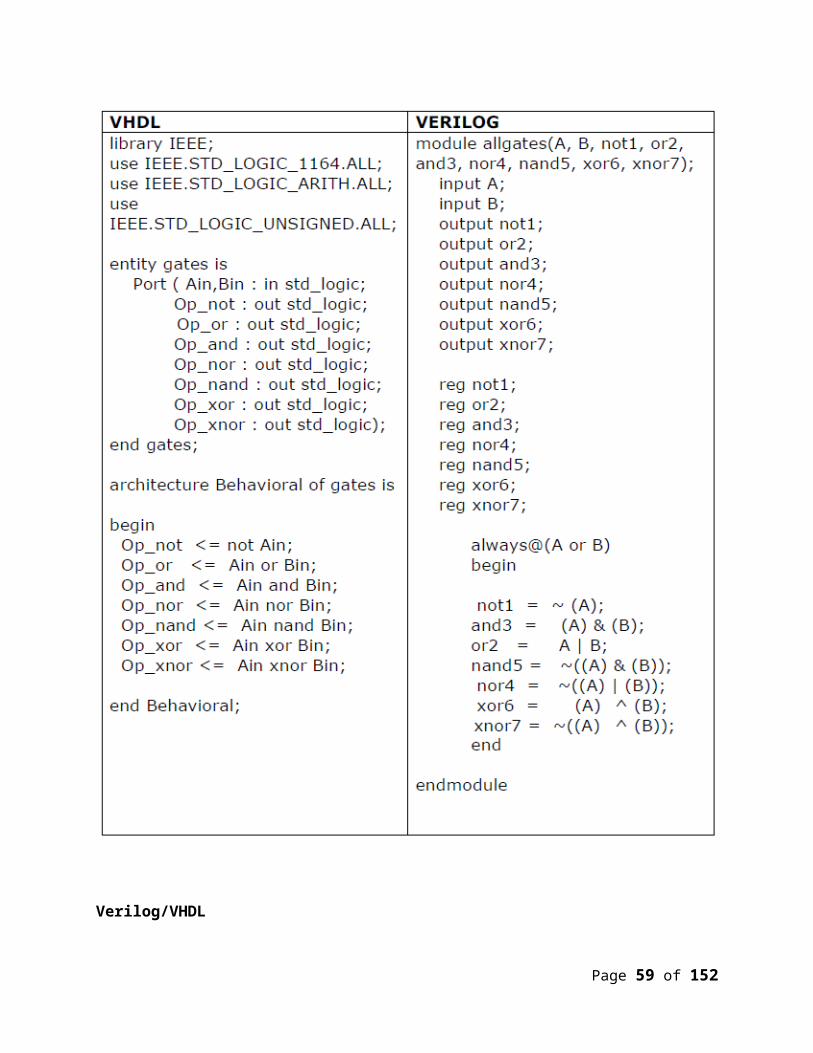
1) Realization of all gates
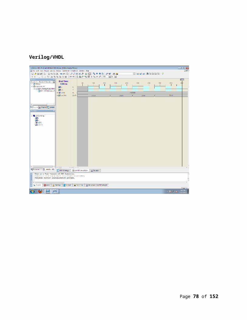
Verilog/VHDL
Page 51 of 132
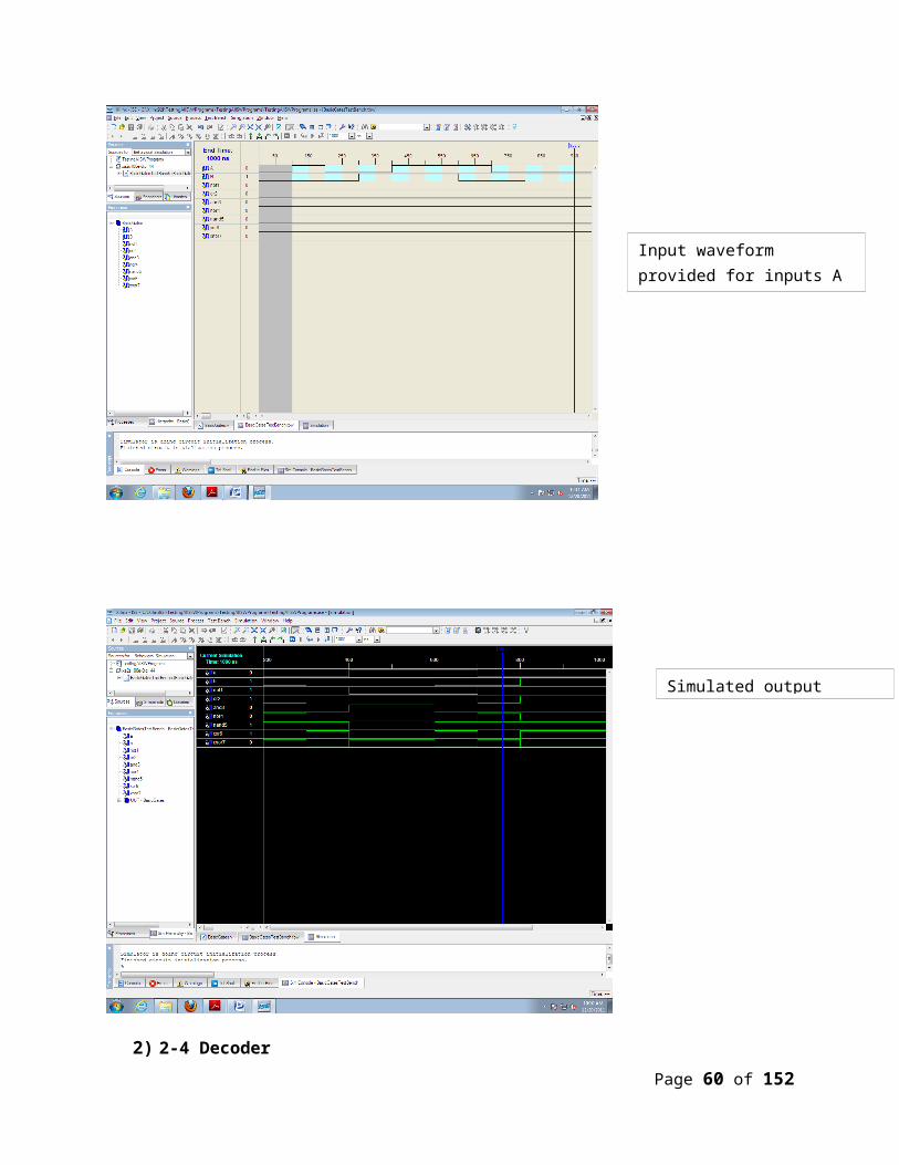
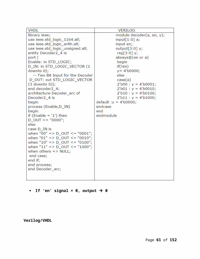
2) 2-4 Decoder
Page 52 of 132
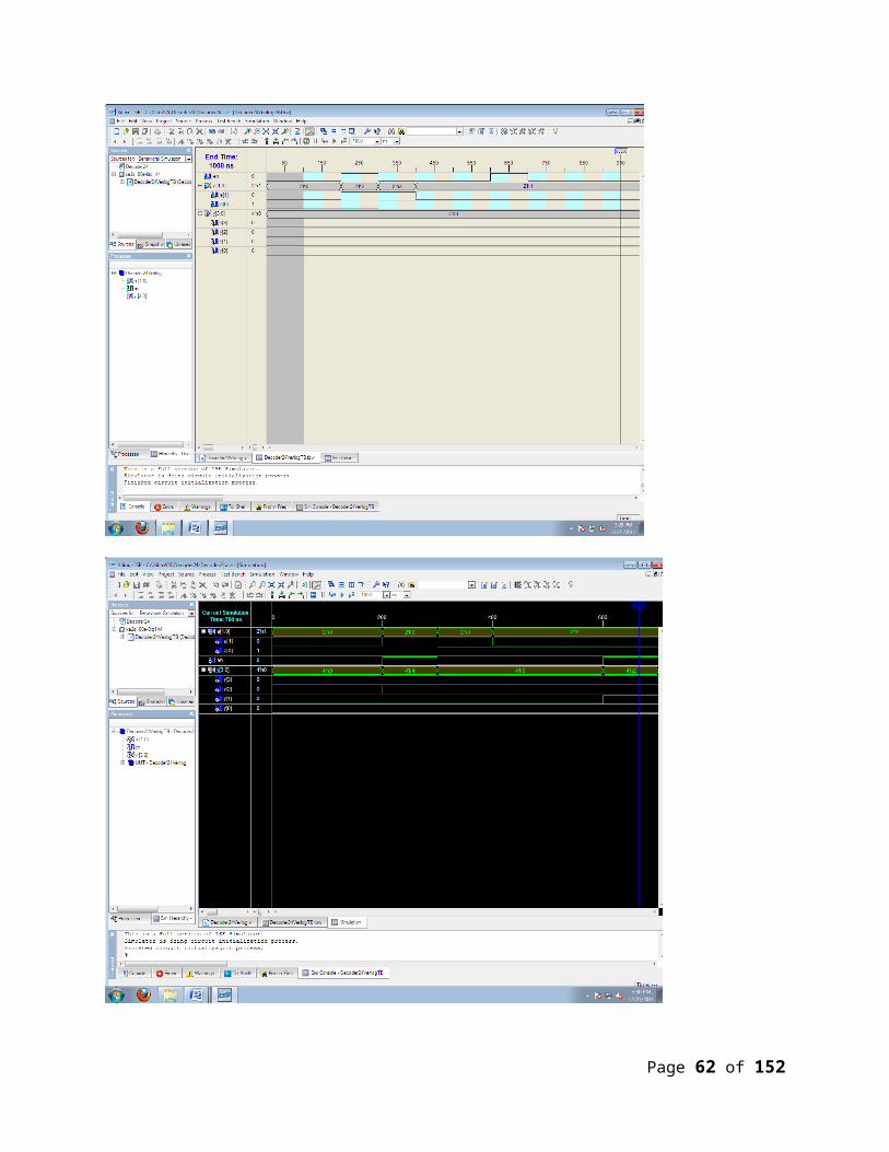
Input waveform provided for inputs A & B
Simulated output waveform
If ‘en’ signal = 0, output 0
Verilog/VHDL
Page 53 of 132
Page 54 of 132
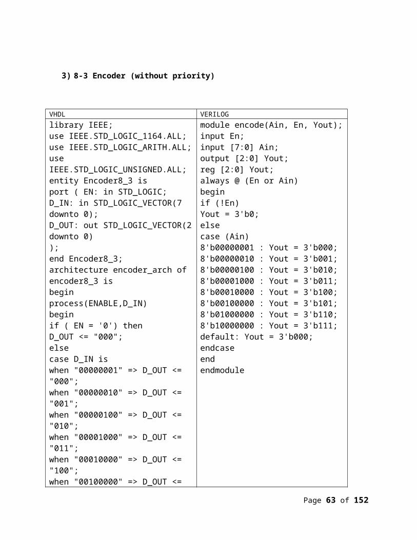
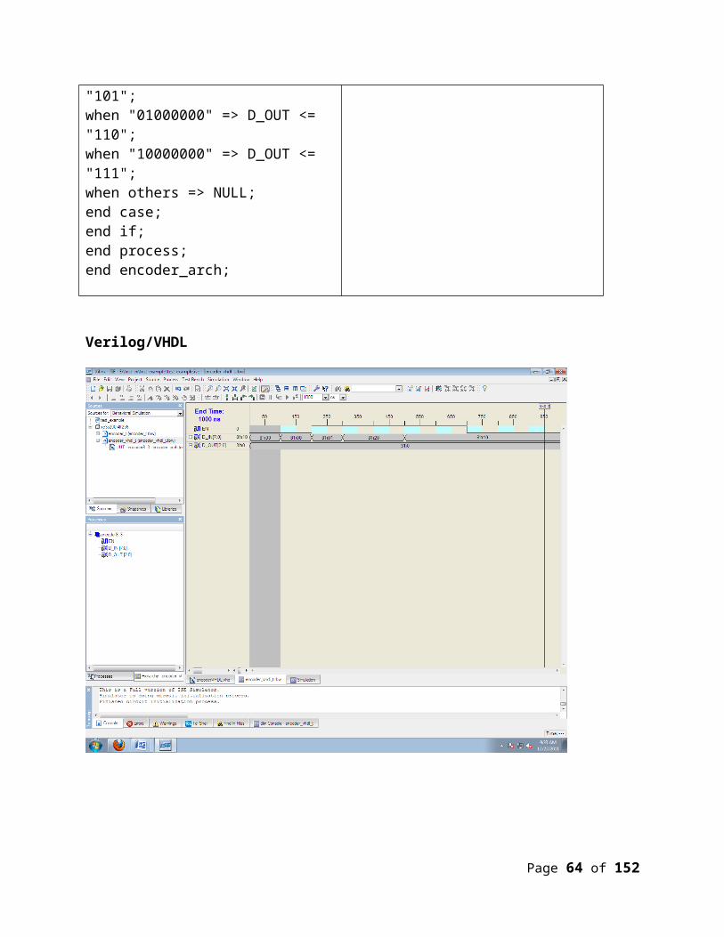
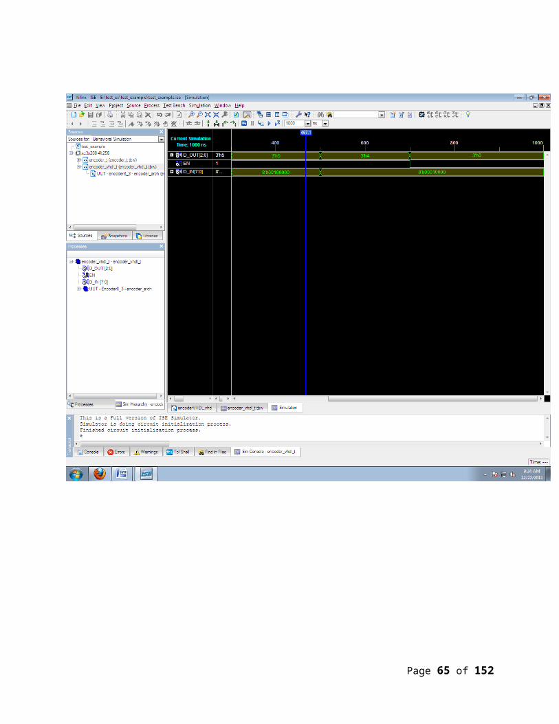
3) 8-3 Encoder (without priority)
VHDL VERILOGlibrary IEEE;use IEEE.STD_LOGIC_1164.ALL; use IEEE.STD_LOGIC_ARITH.ALL; use IEEE.STD_LOGIC_UNSIGNED.ALL; entity Encoder8_3 is port ( EN: in STD_LOGIC; D_IN: in STD_LOGIC_VECTOR(7 downto 0); D_OUT: out STD_LOGIC_VECTOR(2 downto 0) ); end Encoder8_3; architecture encoder_arch of encoder8_3 is begin process(ENABLE,D_IN) begin if ( EN = '0') then D_OUT <= "000"; else case D_IN is when "00000001" => D_OUT <= "000"; when "00000010" => D_OUT <= "001"; when "00000100" => D_OUT <= "010"; when "00001000" => D_OUT <= "011"; when "00010000" => D_OUT <= "100"; when "00100000" => D_OUT <= "101"; when "01000000" => D_OUT <= "110"; when "10000000" => D_OUT <= "111"; when others => NULL; end case; end if;
module encode(Ain, En, Yout); input En; input [7:0] Ain; output [2:0] Yout; reg [2:0] Yout; always @ (En or Ain) begin if (!En) Yout = 3'b0; else case (Ain) 8'b00000001 : Yout = 3'b000; 8'b00000010 : Yout = 3'b001; 8'b00000100 : Yout = 3'b010; 8'b00001000 : Yout = 3'b011; 8'b00010000 : Yout = 3'b100; 8'b00100000 : Yout = 3'b101; 8'b01000000 : Yout = 3'b110; 8'b10000000 : Yout = 3'b111; default: Yout = 3'b000; endcase end endmodule
Page 55 of 132
end process; end encoder_arch;
Verilog/VHDL
Page 56 of 132
Page 57 of 132
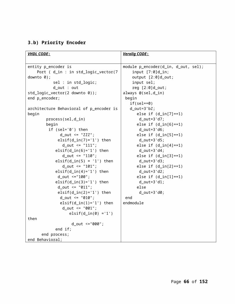
3.b) Priority Encoder
VHDL CODE : Verolig CODE :
entity p_encoder is Port ( d_in : in std_logic_vector(7 downto 0); sel : in std_logic; d_out : out std_logic_vector(2 downto 0));end p_encoder;
architecture Behavioral of p_encoder isbegin
process(sel,d_in) begin if (sel='0') then
d_out <= "ZZZ"; elsif(d_in(7)='1') then d_out <= "111";elsif(d_in(6)='1') then d_out <= "110";elsif(d_in(5) = '1') then d_out <= "101";elsif(d_in(4)='1') then d_out <="100";elsif(d_in(3)='1') then d_out <= "011"; elsif(d_in(2)='1') then d_out <= "010"; elsif(d_in(1)='1') then d_out <= "001";
elsif(d_in(0) ='1') then d_out <="000";
end if;end process;
end Behavioral;
module p_encoder(d_in, d_out, sel); input [7:0]d_in; output [2:0]d_out; input sel; reg [2:0]d_out;always @(sel,d_in) begin if(sel==0) d_out=3’bZ;
else if (d_in[7]==1) d_out=3'd7;else if (d_in[6]==1) d_out=3'd6;else if (d_in[5]==1) d_out=3'd5;else if (d_in[4]==1) d_out=3'd4;else if (d_in[3]==1) d_out=3'd3;else if (d_in[2]==1) d_out=3'd2;else if (d_in[1]==1) d_out=3'd1;else d_out=3'd0;
endendmodule
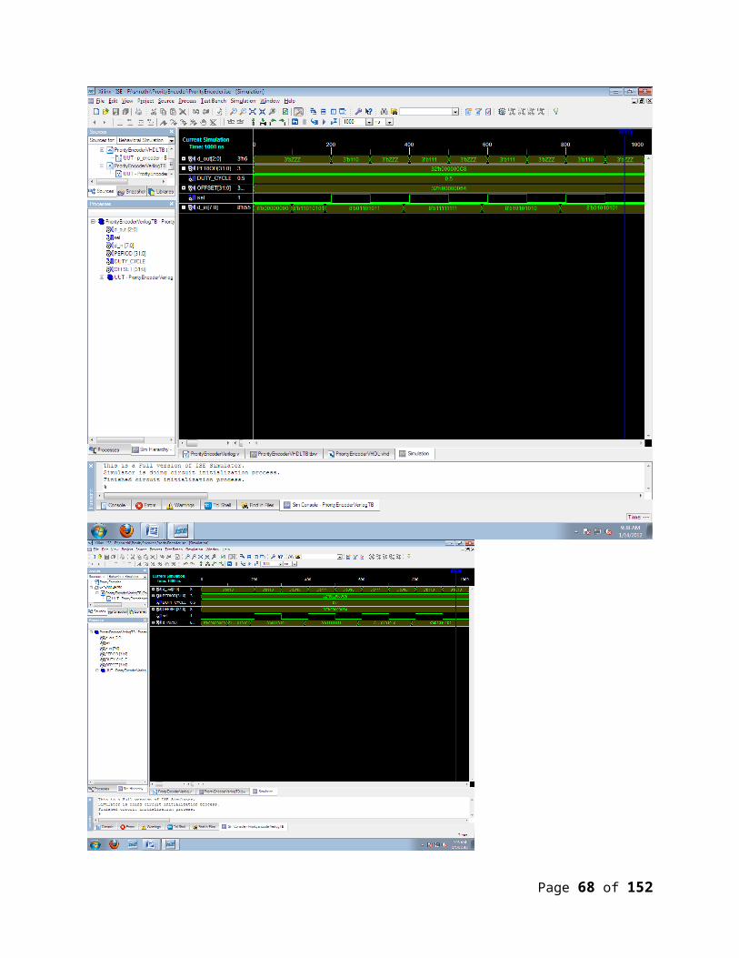
Verilog
Page 58 of 132
Page 59 of 132
Page 60 of 132
VHDL
Page 61 of 132
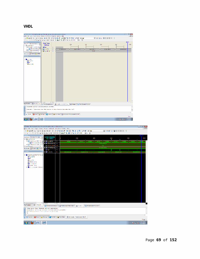
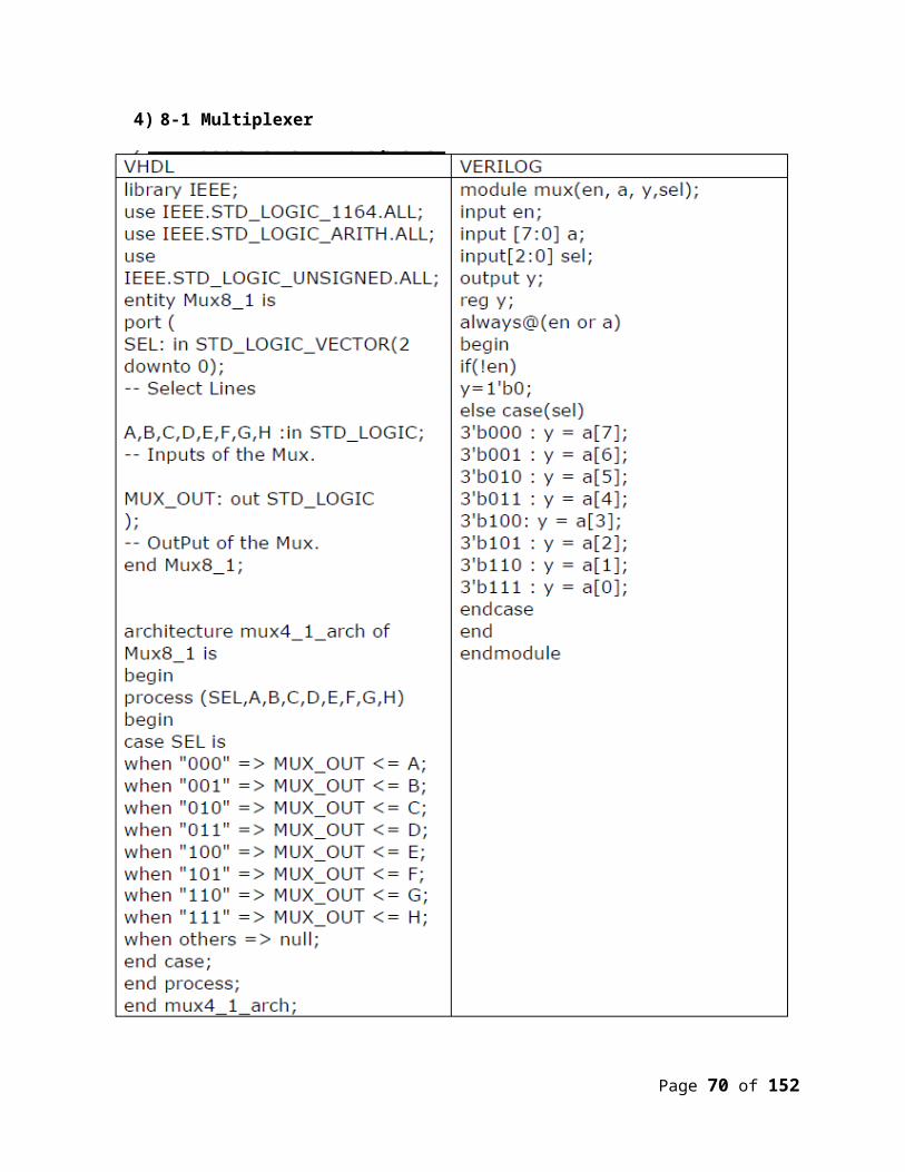
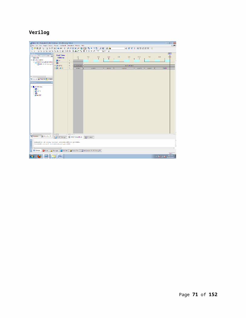
4) 8-1 Multiplexer
Page 62 of 132
Verilog
Page 63 of 132
VHDL
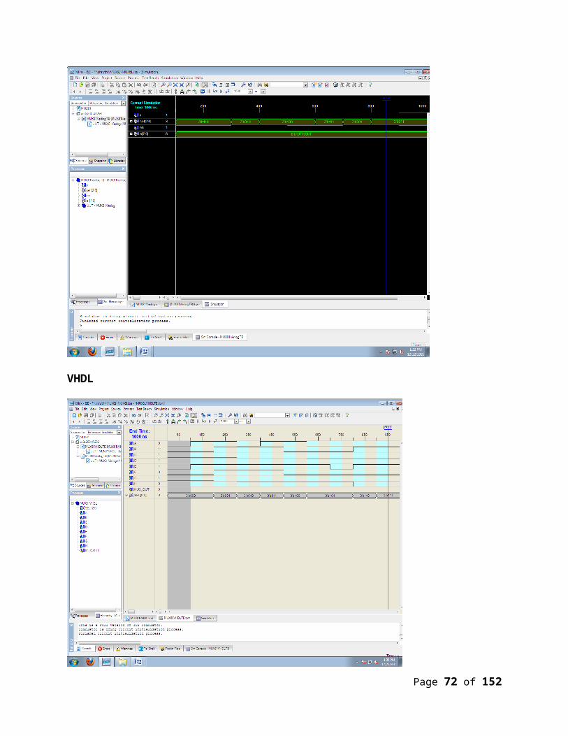
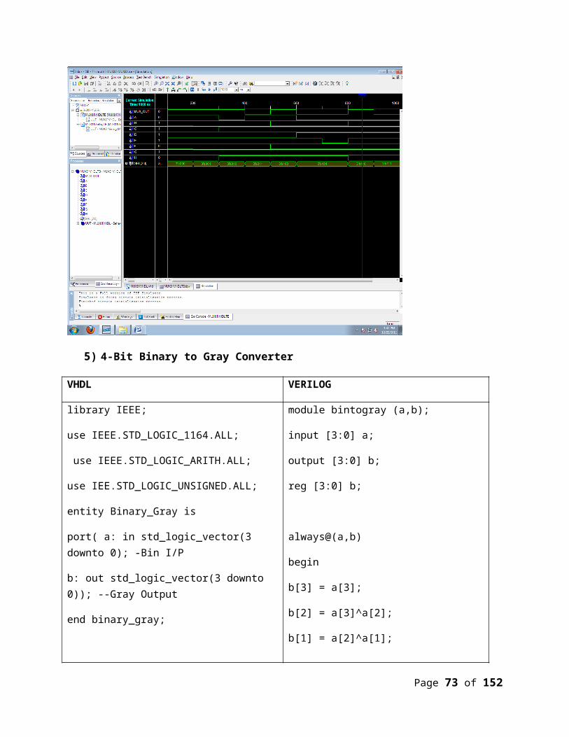
5) 4-Bit Binary to Gray Converter
Page 64 of 132
VHDL VERILOG
library IEEE;
use IEEE.STD_LOGIC_1164.ALL;
use IEEE.STD_LOGIC_ARITH.ALL;
use IEE.STD_LOGIC_UNSIGNED.ALL;
entity Binary_Gray is
port( a: in std_logic_vector(3 downto 0); -Bin I/P
b: out std_logic_vector(3 downto 0)); --Gray Output
end binary_gray;
architecture behavioral of binary_gray is begin
b(3)<= a(3);
b(2)<= a(3) xor a(2);
b(1)<= a(2) xor a(1);
b(0)<= a(1) xor a(0);
end behavioral;
module bintogray (a,b);
input [3:0] a;
output [3:0] b;
reg [3:0] b;
always@(a,b)
begin
b[3] = a[3];
b[2] = a[3]^a[2];
b[1] = a[2]^a[1];
b[0] = a[1]^a[0];
end
endmodule
Verilog/VHDL
Page 65 of 132
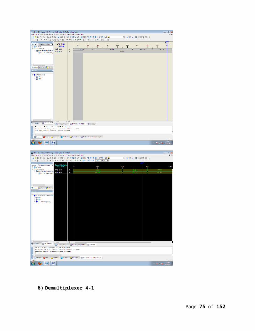
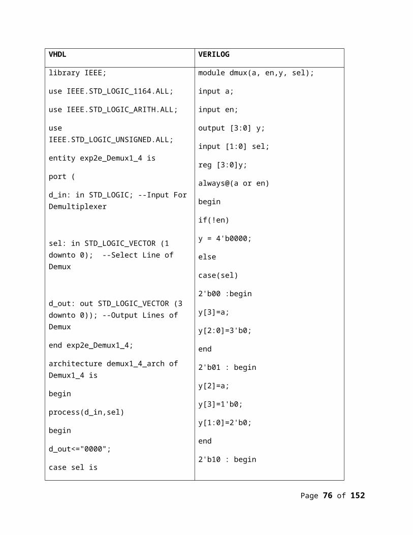
6) Demultiplexer 4-1
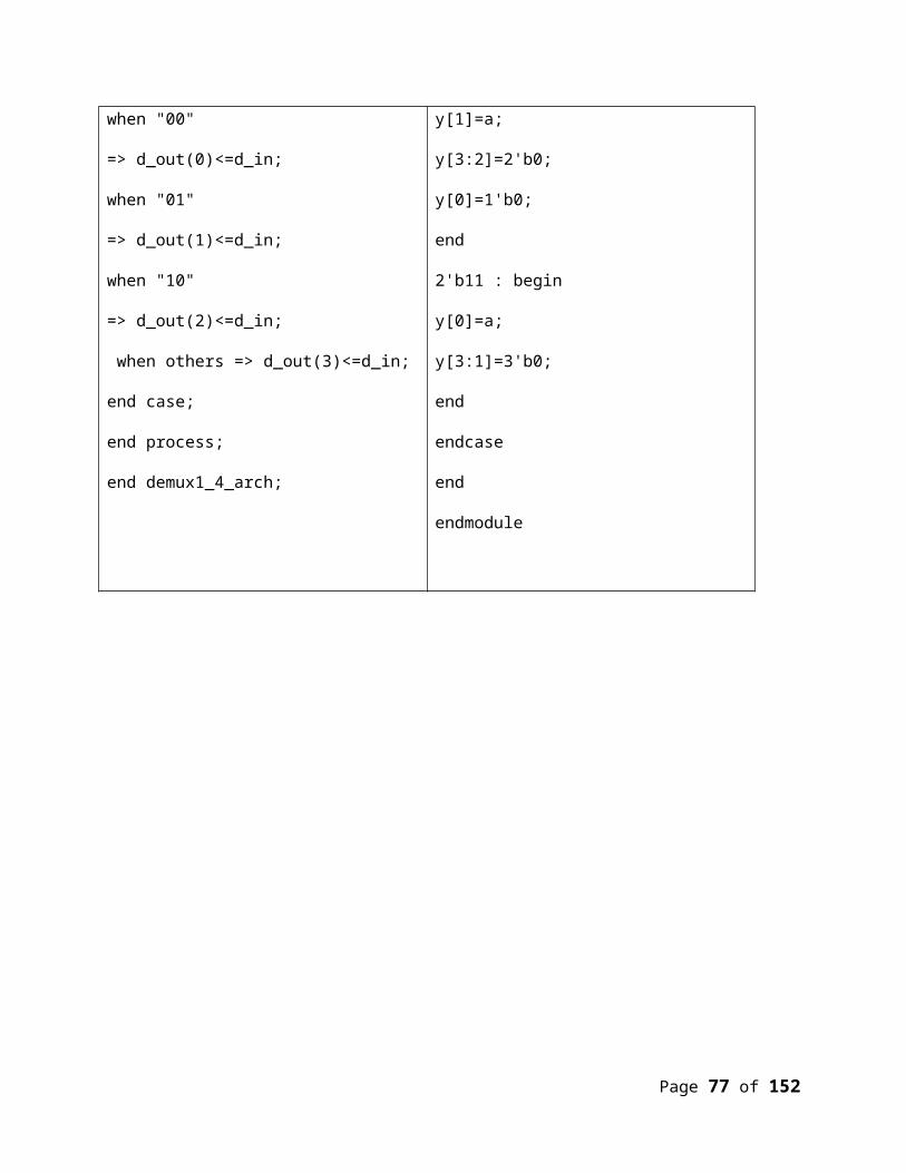
VHDL VERILOG
Page 66 of 132
library IEEE;
use IEEE.STD_LOGIC_1164.ALL;
use IEEE.STD_LOGIC_ARITH.ALL;
use IEEE.STD_LOGIC_UNSIGNED.ALL;
entity exp2e_Demux1_4 is
port (
d_in: in STD_LOGIC; --Input For Demultiplexer
sel: in STD_LOGIC_VECTOR (1 downto 0); --Select Line of Demux
d_out: out STD_LOGIC_VECTOR (3 downto 0)); --Output Lines of Demux
end exp2e_Demux1_4;
architecture demux1_4_arch of Demux1_4 is
begin
process(d_in,sel)
begin
d_out<="0000";
case sel is
when "00"
=> d_out(0)<=d_in;
when "01"
=> d_out(1)<=d_in;
module dmux(a, en,y, sel);
input a;
input en;
output [3:0] y;
input [1:0] sel;
reg [3:0]y;
always@(a or en)
begin
if(!en)
y = 4'b0000;
else
case(sel)
2'b00 :begin
y[3]=a;
y[2:0]=3'b0;
end
2'b01 : begin
y[2]=a;
y[3]=1'b0;
y[1:0]=2'b0;
end
2'b10 : begin
y[1]=a;
y[3:2]=2'b0;
y[0]=1'b0;
Page 67 of 132
when "10"
=> d_out(2)<=d_in;
when others => d_out(3)<=d_in;
end case;
end process;
end demux1_4_arch;
end
2'b11 : begin
y[0]=a;
y[3:1]=3'b0;
end
endcase
end
endmodule
Verilog/VHDL
Page 68 of 132
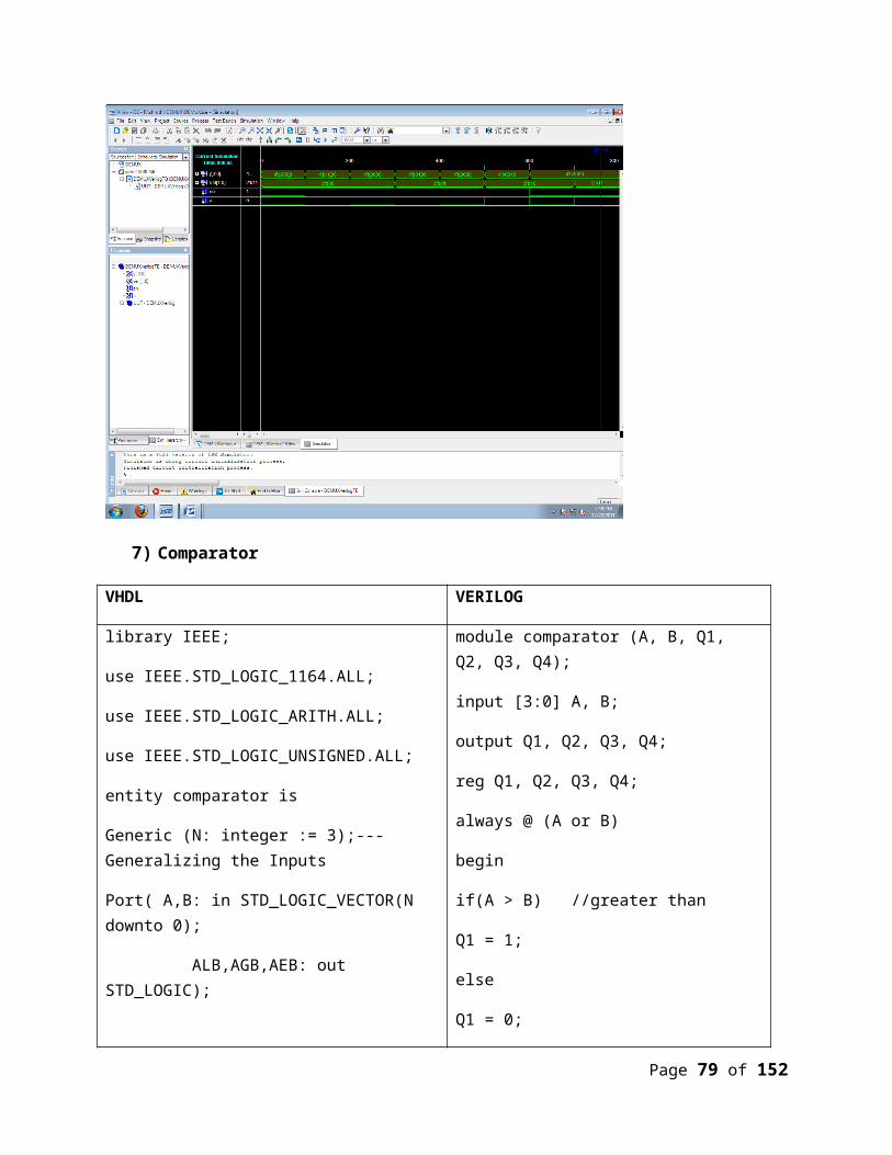
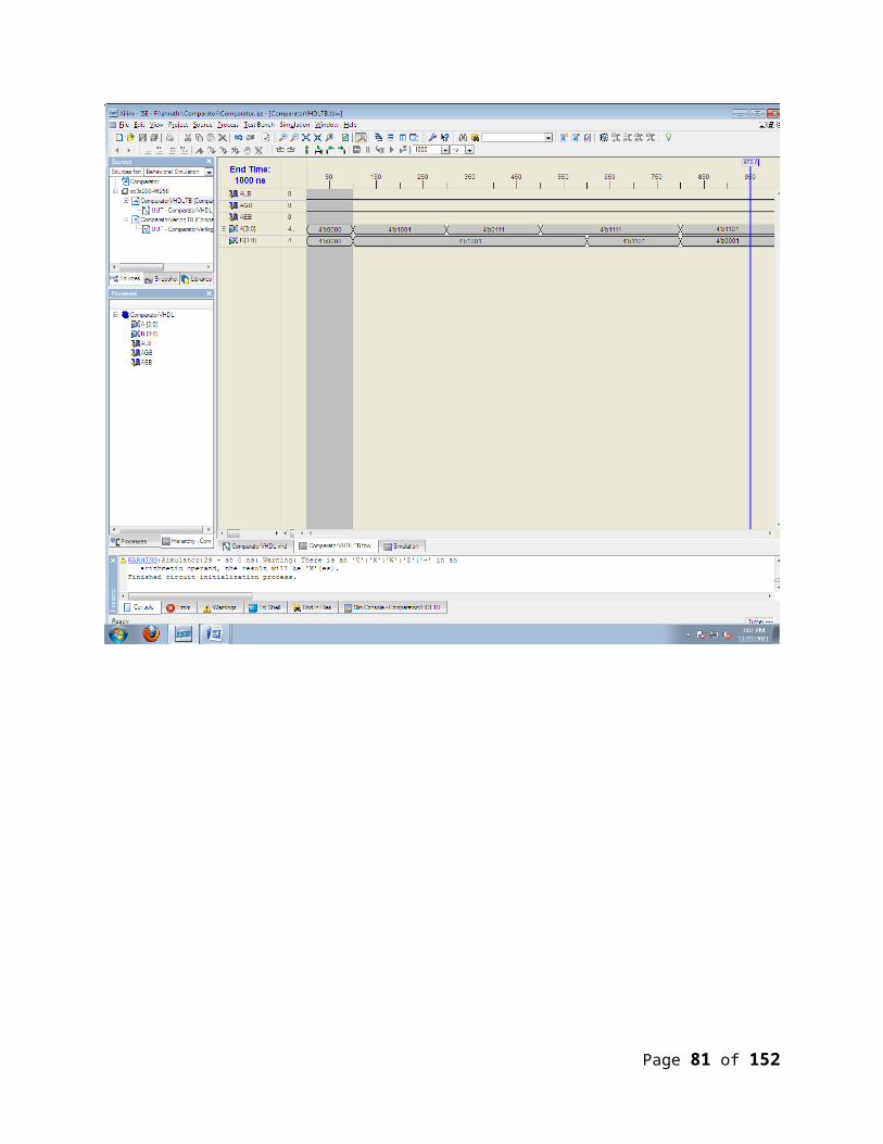
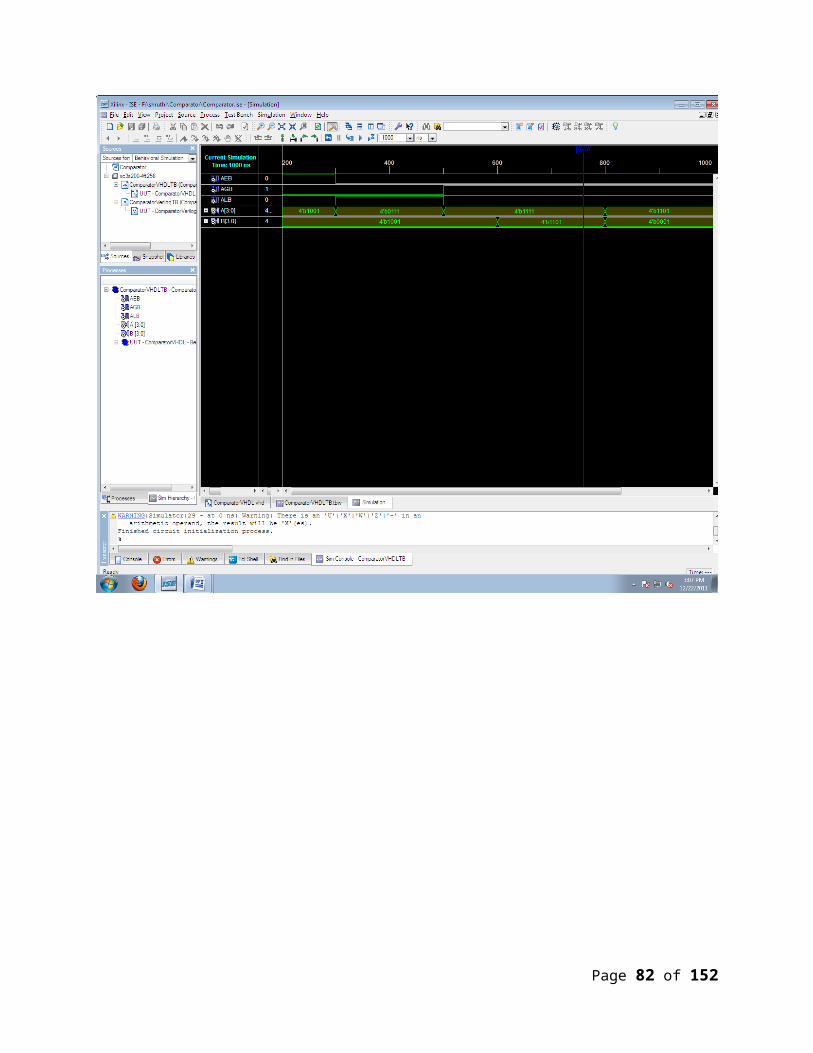
7) Comparator
Page 69 of 132
VHDL VERILOG
library IEEE;
use IEEE.STD_LOGIC_1164.ALL;
use IEEE.STD_LOGIC_ARITH.ALL;
use IEEE.STD_LOGIC_UNSIGNED.ALL;
entity comparator is
Generic (N: integer := 3);--- Generalizing the Inputs
Port( A,B: in STD_LOGIC_VECTOR(N downto 0);
ALB,AGB,AEB: out STD_LOGIC);
end comparator;
architecture Comparator_arc of comparator is
begin
process(A,B)
begin
if ( A < B ) then ALB <= '1';
else ALB <= '0';
end if;
if ( A > B ) then AGB <= '1';
else AGB <= '0';
end if;
if ( A = B ) then AEB <= '1';
else AEB <= '0';
end if;
module comparator (A, B, Q1, Q2, Q3, Q4);
input [3:0] A, B;
output Q1, Q2, Q3, Q4;
reg Q1, Q2, Q3, Q4;
always @ (A or B)
begin
if(A > B) //greater than
Q1 = 1;
else
Q1 = 0;
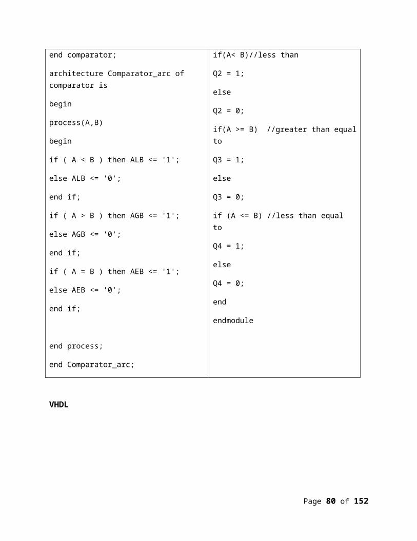
if(A< B)//less than
Q2 = 1;
else
Q2 = 0;
if(A >= B) //greater than equal to
Q3 = 1;
else
Q3 = 0;
if (A <= B) //less than equal to
Q4 = 1;
else
Q4 = 0;
end
endmodule
Page 70 of 132
end process;
end Comparator_arc;
VHDL
Page 71 of 132
Page 72 of 132
8) HDL Code For HALF ADDER & FULL ADDER (Structural)
VHDL VERILOG
library IEEE;
use IEEE.STD_LOGIC_1164.ALL;
use IEEE.STD_LOGIC_ARITH.ALL;
use IEEE.STD_LOGIC_UNSIGNED.ALL;
entity Halfadder is
Port ( Ain, Bin : in std_logic; --2Bit Input
Sum, Carry : out std_logic); --sum& carry
end exp3_Halfadder;
architecture Behavioral of exp3_Halfadder is
begin
Sum <= Ain xor Bin;
Carry<= Ain and Bin;
end Behavioral;
********************************
FOR FULL ADDR
library IEEE;
use IEEE.STD_LOGIC_1164.ALL;
use IEEE.STD_LOGIC_ARITH.ALL;
use IEEE.STD_LOGIC_UNSIGNED.ALL;
entity FullAdder is
Port ( Ain : in std_logic;
--Input One
module halfadder(a,b,carry,sum);
input a;
input b;
output carry;
output sum;
assignsum = a ^ b;
assign carry = a & b;
endmodule
***************************
FOR FULL ADDER
module adder(Ain,Bin,Cin,Carry,Sum);
input Ain;
input Bin;
input Cin;
wire w1,w2,w3;
output Carry;
output Sum;
Page 73 of 132
Bin : in std_logic;
--Input Two
Cin : in std_logic;
--Carry Input
Cout : out std_logic; --Carry Output
Sum : out std_logic); --Sum Output
end exp3_FullAdder;
architecture Behavioral of FullAdder is
-- Half Adder Component being Instantiated
Component exp3_Halfadder Port ( Ain : in std_logic; Bin : in std_logic; Sum : out std_logic; Carry : out std_logic);
end Component;
Signal temp1,temp2, temp3: std_logic; -- Signal Declaration
begin -- Port Mapping of Component (By Positional Mapping Method)
L1: Halfadder port map( Ain, Bin,temp1,temp2);
L2: Half adder port map( temp1,Cin,Sum,temp3);
Cout <= temp2 or temp3;
end Behavioral;
exp5_halfadder L1(Ain, Bin, w1, w2);
exp5_halfadder L2(Cin, w2, w3, Sum);
assign Carry = w1|w3;
endmodule
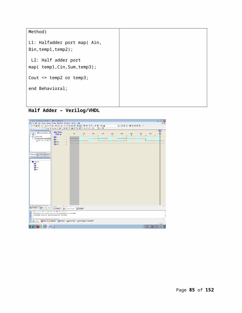
Half Adder – Verilog/VHDL
Page 74 of 132
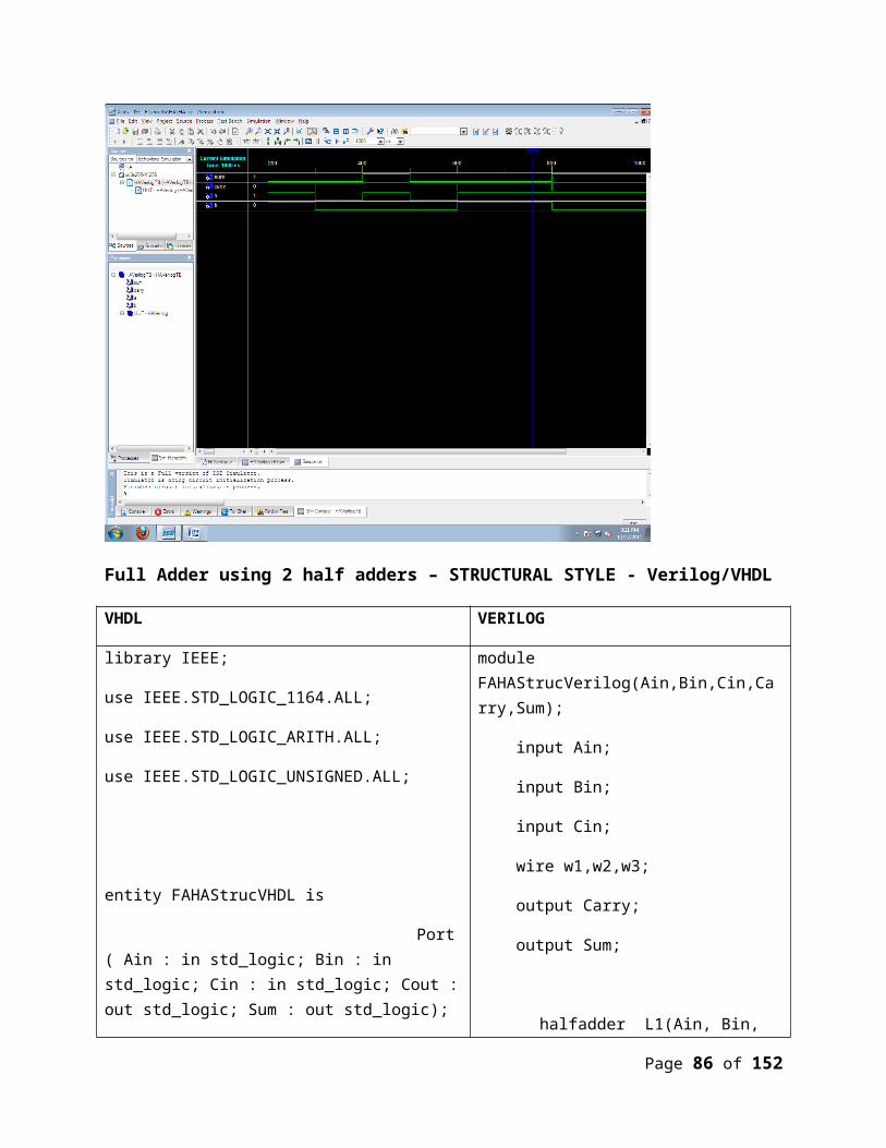
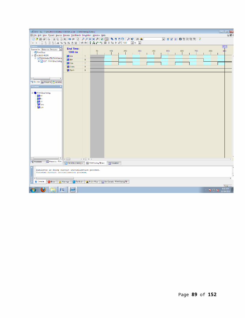
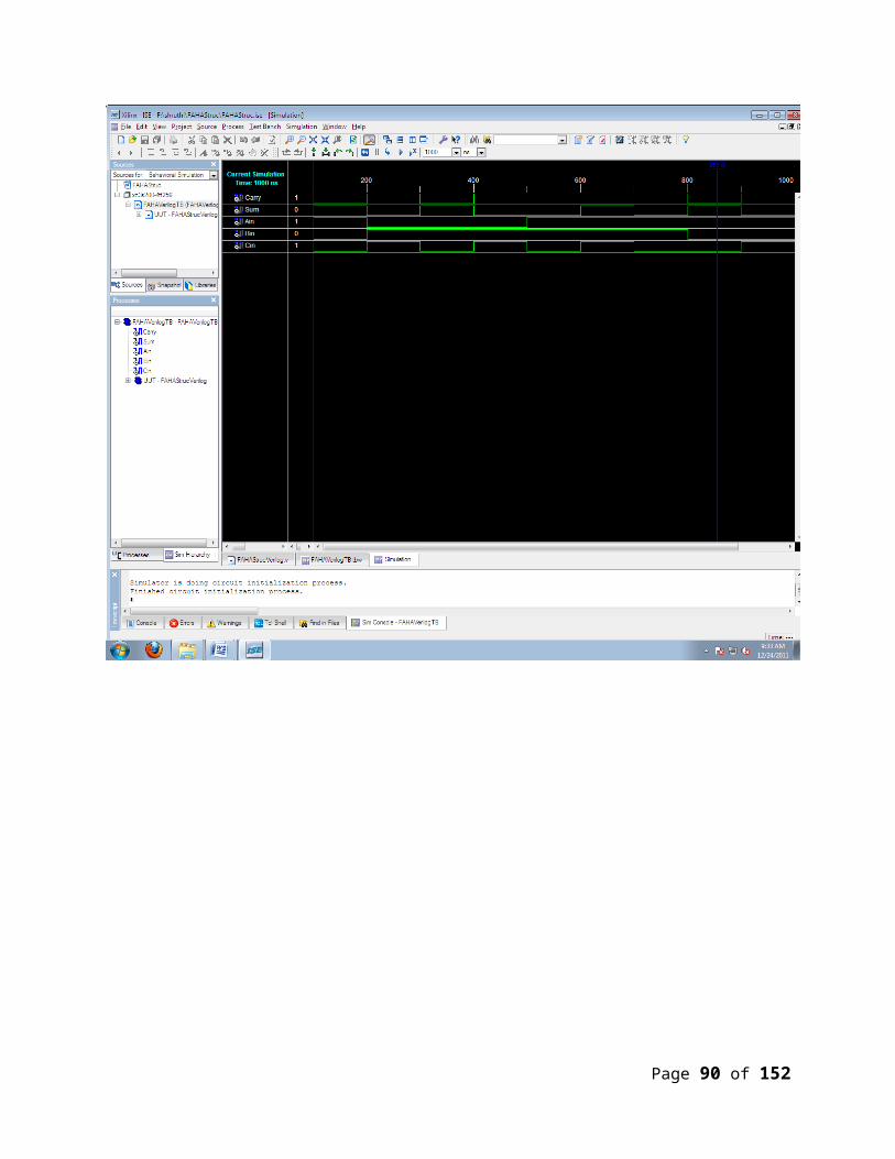
Full Adder using 2 half adders – STRUCTURAL STYLE - Verilog/VHDL
Page 75 of 132
VHDL VERILOG
library IEEE;
use IEEE.STD_LOGIC_1164.ALL;
use IEEE.STD_LOGIC_ARITH.ALL;
use IEEE.STD_LOGIC_UNSIGNED.ALL;
entity FAHAStrucVHDL is
Port ( Ain : in std_logic; Bin : in std_logic; Cin : in std_logic; Cout : out std_logic; Sum : out std_logic);
end FAHAStrucVHDL;
architecture Behavioral of FAHAStrucVHDL is
component Halfadder
Port ( Ain : in std_logic; Bin : in std_logic; Sum : out std_logic; Carry : out std_logic);
end Component;
signal temp1,temp2, temp3: std_logic;
begin
L1: Halfadder port map( Ain, Bin,temp1,temp2);
L2: Halfadder port
module FAHAStrucVerilog(Ain,Bin,Cin,Carry,Sum);
input Ain;
input Bin;
input Cin;
wire w1,w2,w3;
output Carry;
output Sum;
halfadder L1(Ain, Bin, w1, w2);
halfadder L2(Cin, w2, w3, Sum);
assign Carry = w1|w3;
endmodule
module halfadder (a,b,carry,sum);
input a;
input b;
output carry;
output sum;
assignsum = a ^ b;
Page 76 of 132
map( temp1,Cin,Sum,temp3);
Cout <= temp2 or temp3;
end Behavioral;
library IEEE;
use IEEE.STD_LOGIC_1164.ALL;
use IEEE.STD_LOGIC_ARITH.ALL;
use IEEE.STD_LOGIC_UNSIGNED.ALL;
entity Halfadder is
Port ( Ain, Bin : in std_logic;
Sum, Carry : out std_logic);
end Halfadder;
architecture Behavioral of Halfadder is
begin
Sum <= Ain xor Bin;
Carry<= Ain and Bin;
end Behavioral;
assign carry = a & b;
endmodule
#NOTE: The order of programs can be anything i.e. order of main module and sub module
Verilog/VHDL
Page 77 of 132
Page 78 of 132
Page 79 of 132
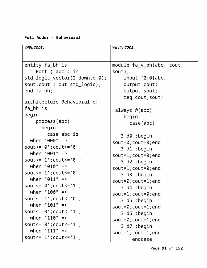
Full Adder – Behavioral
VHDL CODE : Verolig CODE :
entity fa_bh is Port ( abc : in std_logic_vector(2 downto 0); sout,cout : out std_logic);end fa_bh;
architecture Behavioral of fa_bh isbegin process(abc) begin case abc is when "000" => sout<='0';cout<='0'; when "001" => sout<='1';cout<='0'; when "010" => sout<='1';cout<='0'; when "011" => sout<='0';cout<='1'; when "100" => sout<='1';cout<='0'; when "101" => sout<='0';cout<='1'; when "110" => sout<='0';cout<='1'; when "111" => sout<='1';cout<='1'; when others=> null; end case; end process;end Behavioral;
module fa_v_bh(abc, cout, sout); input [2:0]abc; output cout; output sout; reg cout,sout;
always @(abc) begin case(abc) 3'd0 :begin sout=0;cout=0;end 3'd1 :begin sout=1;cout=0;end 3'd2 :begin sout=1;cout=0;end 3'd3 :begin sout=0;cout=1;end 3'd4 :begin sout=1;cout=0;end 3'd5 :begin sout=0;cout=1;end 3'd6 :begin sout=0;cout=1;end 3'd7 :begin sout=1;cout=1;end endcase endendmodule
Page 80 of 132
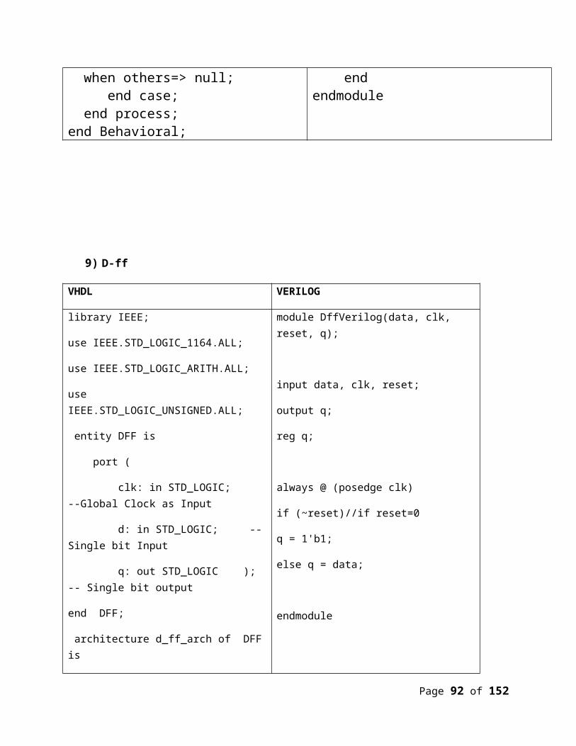
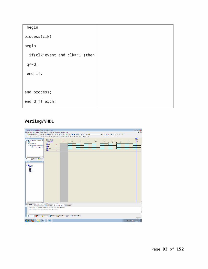
9) D-ff
VHDL VERILOG
library IEEE;
use IEEE.STD_LOGIC_1164.ALL;
use IEEE.STD_LOGIC_ARITH.ALL;
use IEEE.STD_LOGIC_UNSIGNED.ALL;
entity DFF is
port (
clk: in STD_LOGIC; --Global Clock as Input
d: in STD_LOGIC; -- Single bit Input
q: out STD_LOGIC ); -- Single bit output
end DFF;
architecture d_ff_arch of DFF is
begin
process(clk)
begin
if(clk'event and clk='1')then
q<=d;
end if;
end process;
end d_ff_arch;
module DffVerilog(data, clk, reset, q);
input data, clk, reset;
output q;
reg q;
always @ (posedge clk)
if (~reset)//if reset=0
q = 1'b1;
else q = data;
endmodule
Verilog/VHDL
Page 81 of 132
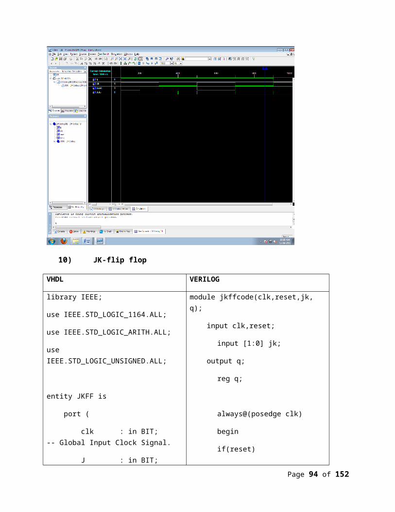
10) JK-flip flop
Page 82 of 132
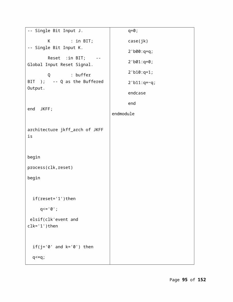
VHDL VERILOG
library IEEE;
use IEEE.STD_LOGIC_1164.ALL;
use IEEE.STD_LOGIC_ARITH.ALL;
use IEEE.STD_LOGIC_UNSIGNED.ALL;
entity JKFF is
port (
clk : in BIT; -- Global Input Clock Signal.
J : in BIT; -- Single Bit Input J.
K : in BIT; -- Single Bit Input K.
Reset :in BIT; -- Global Input Reset Signal.
Q : buffer BIT ); -- Q as the Buffered Output.
end JKFF;
architecture jkff_arch of JKFF is
begin
process(clk,reset)
begin
if(reset='1')then
module jkffcode(clk,reset,jk, q);
input clk,reset;
input [1:0] jk;
output q;
reg q;
always@(posedge clk)
begin
if(reset)
q=0;
case(jk)
2'b00:q=q;
2'b01:q=0;
2'b10:q=1;
2'b11:q=~q;
endcase
end
endmodule
Page 83 of 132
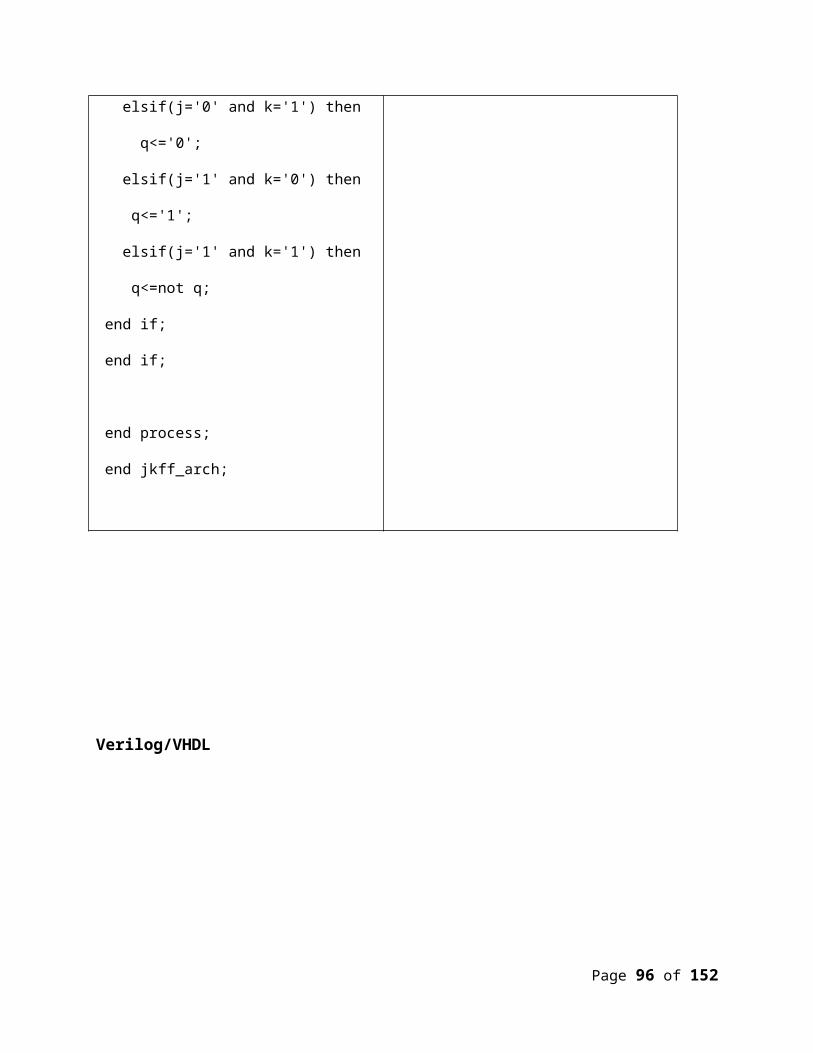
q<='0';
elsif(clk'event and clk='1')then
if(j='0' and k='0') then
q<=q;
elsif(j='0' and k='1') then
q<='0';
elsif(j='1' and k='0') then
q<='1';
elsif(j='1' and k='1') then
q<=not q;
end if;
end if;
end process;
end jkff_arch;
Verilog/VHDL
Page 84 of 132
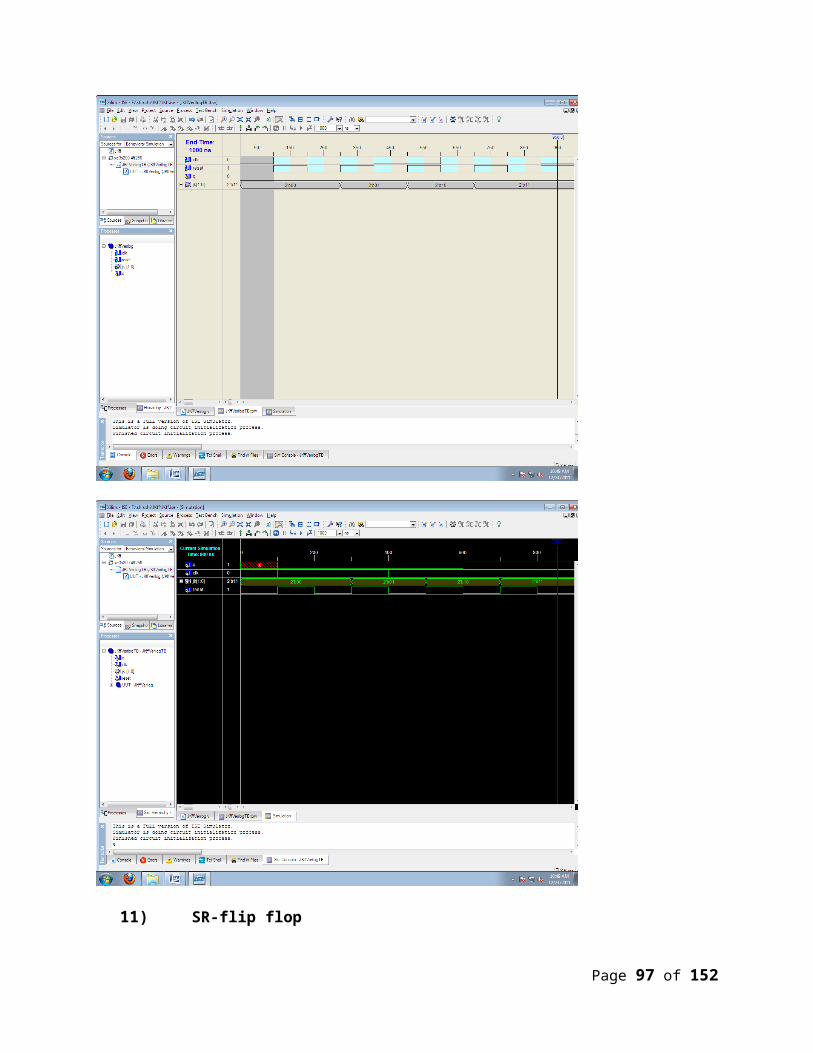
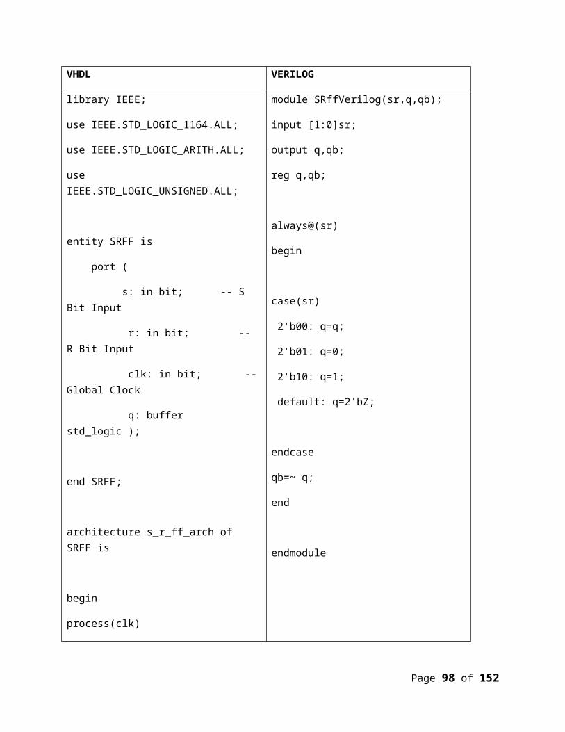
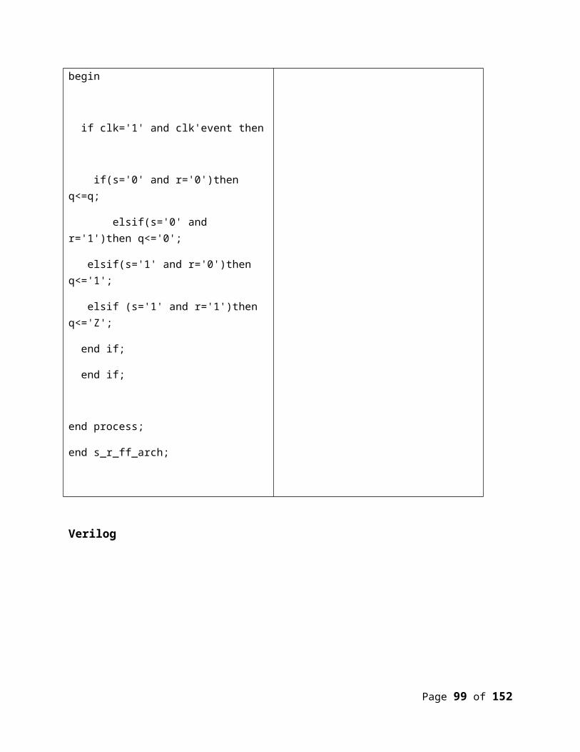
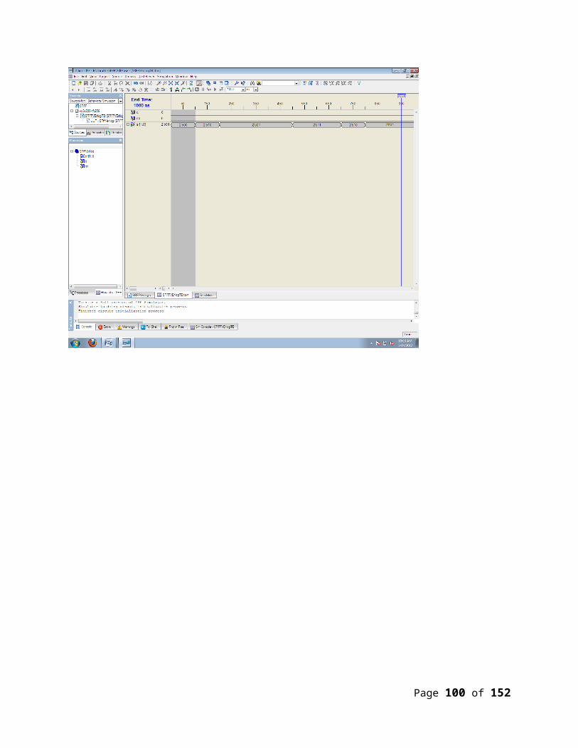
11) SR-flip flop
Page 85 of 132
VHDL VERILOG
library IEEE;
use IEEE.STD_LOGIC_1164.ALL;
use IEEE.STD_LOGIC_ARITH.ALL;
use IEEE.STD_LOGIC_UNSIGNED.ALL;
entity SRFF is
port (
s: in bit; -- S Bit Input
r: in bit; -- R Bit Input
clk: in bit; -- Global Clock
q: buffer std_logic );
end SRFF;
architecture s_r_ff_arch of SRFF is
begin
process(clk)
begin
if clk='1' and clk'event then
if(s='0' and r='0')then q<=q;
elsif(s='0' and r='1')then q<='0';
module SRffVerilog(sr,q,qb);
input [1:0]sr;
output q,qb;
reg q,qb;
always@(sr)
begin
case(sr)
2'b00: q=q;
2'b01: q=0;
2'b10: q=1;
default: q=2'bZ;
endcase
qb=~ q;
end
endmodule
Page 86 of 132
elsif(s='1' and r='0')then q<='1';
elsif (s='1' and r='1')then q<='Z';
end if;
end if;
end process;
end s_r_ff_arch;
Verilog
Page 87 of 132
VHDL
Page 88 of 132
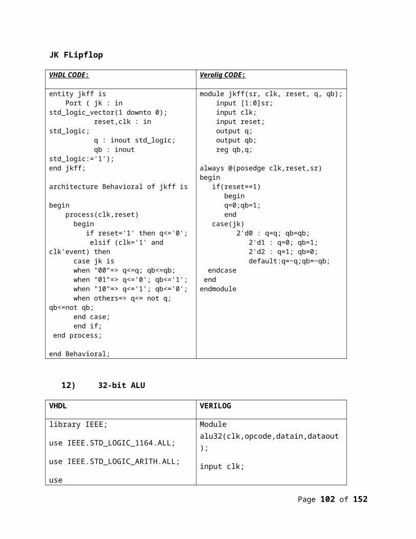
JK FLipflop
VHDL CODE : Verolig CODE :
entity jkff is Port ( jk : in std_logic_vector(1 downto 0); reset,clk : in std_logic; q : inout std_logic; qb : inout std_logic:='1');end jkff;
architecture Behavioral of jkff is
begin process(clk,reset)
begin if reset='1' then q<='0'; elsif (clk='1' and clk'event) thencase jk is when "00"=> q<=q; qb<=qb;when "01"=> q<='0'; qb<='1';when "10"=> q<='1'; qb<='0';when others=> q<= not q; qb<=not qb;end case;
end if; end process;
end Behavioral;
module jkff(sr, clk, reset, q, qb); input [1:0]sr; input clk; input reset; output q; output qb; reg qb,q;
always @(posedge clk,reset,sr)begin if(reset==1)
begin q=0;qb=1;
end case(jk)
2'd0 : q=q; qb=qb;2'd1 : q=0; qb=1;2'd2 : q=1; qb=0;default:q=~q;qb=~qb;
endcase endendmodule
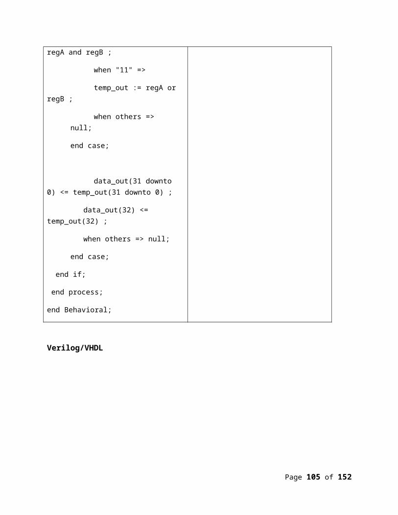
12) 32-bit ALU
VHDL VERILOG
library IEEE;
use IEEE.STD_LOGIC_1164.ALL;
use IEEE.STD_LOGIC_ARITH.ALL;
use IEEE.STD_LOGIC_UNSIGNED.ALL;
-- Uncomment the following lines to use the declarations that are
-- provided for instantiating Xilinx primitive components.
--library UNISIM;
Module alu32(clk,opcode,datain,dataout);
input clk;
input [3:0] opcode;
input [31:0] datain;
output [32:0] dataout;
//reg [32:0] temp;
reg [32:0] dataout;
Page 89 of 132
--use UNISIM.VComponents.all;
entity alu_8bit is
Port ( clk : std_logic;
data : in std_logic_vector(3 downto 0);
data_in : in std_logic_vector(31 downto 0);
data_out : out std_logic_vector(32 downto 0));
end alu_8bit;
architecture Behavioral of alu_8bit is
begin
process(clk)
variable temp_out : std_logic_vector(32 downto 0):=(others=>'0');
--variable temp_out1 : std_logic_vector(8 downto 0):=(others=>'0');
variable regA,regB : std_logic_vector(31 downto 0):=(others=>'0');
begin
if rising_edge(clk) then
case data(3 downto 2) is
when "00" =>
regA(31 downto 0) := data_in(31 downto 0);
reg [31:0] a,b;
always@(posedge clk)
begin
case(opcode[3:2])
2'b00:a=datain;
2'b01:b=datain;
2'b10:
case(opcode[1:0])
2'b00:dataout=a+b;
2'b01:dataout=a-b;
2'b10:dataout=a&b;
2'b11:dataout=a|b;
default dataout=a&b;
endcase
2'b11:dataout=dataout;
endcase
end
endmodule
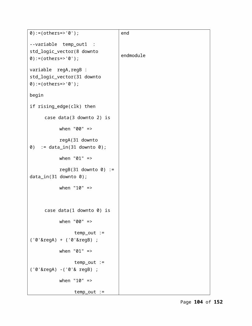
Page 90 of 132
when "01" =>
regB(31 downto 0) := data_in(31 downto 0);
when "10" =>
case data(1 downto 0) is
when "00" =>
temp_out := ('0'®A) + ('0'®B) ;
when "01" =>
temp_out := ('0'®A) -('0'& regB) ;
when "10" =>
temp_out := regA and regB ;
when "11" =>
temp_out := regA or regB ;
when others => null;
end case;
data_out(31 downto 0) <= temp_out(31 downto 0) ;
data_out(32) <= temp_out(32) ;
when others => null;
end case;
end if;
end process;
Page 91 of 132
end Behavioral;
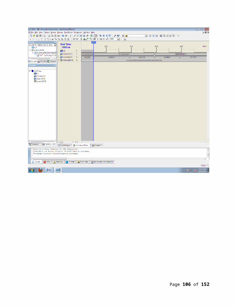
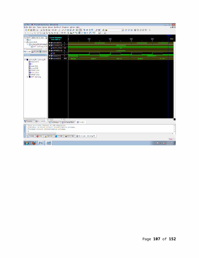
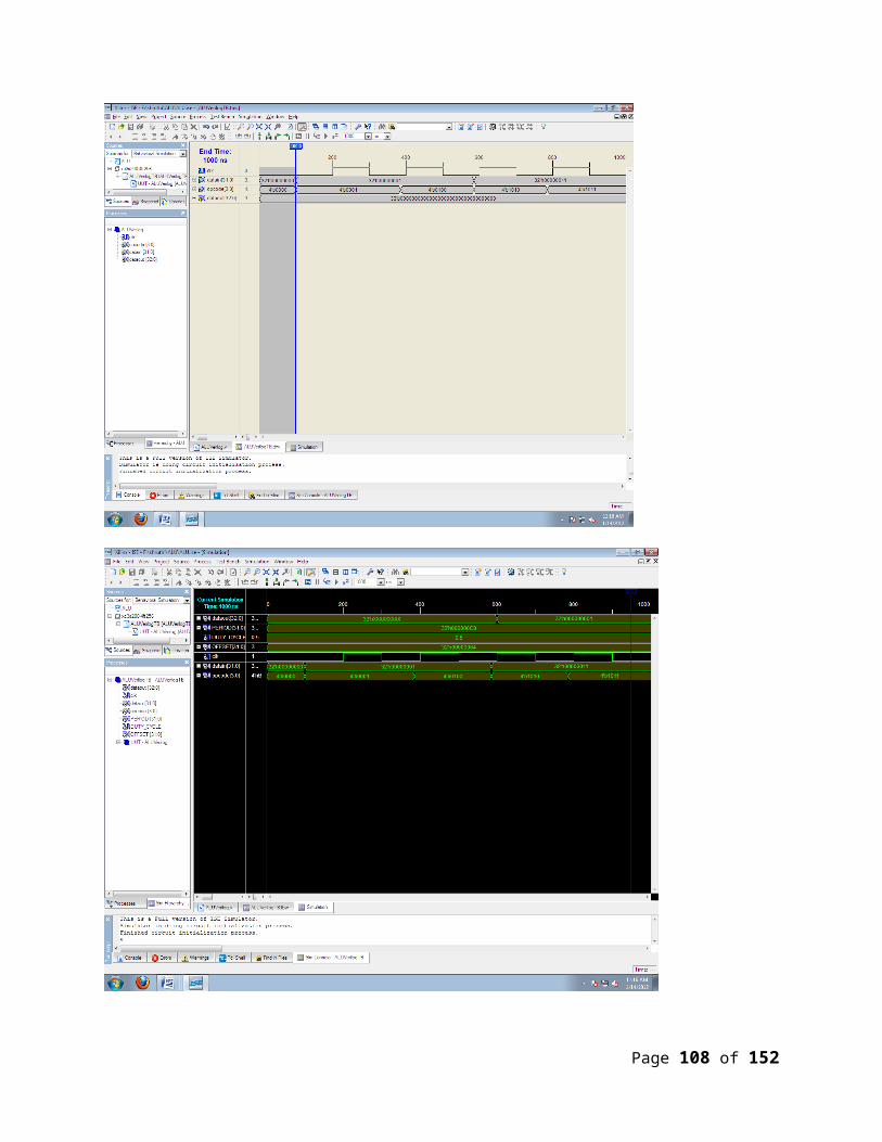
Verilog/VHDL
Page 92 of 132
Page 93 of 132
Page 94 of 132
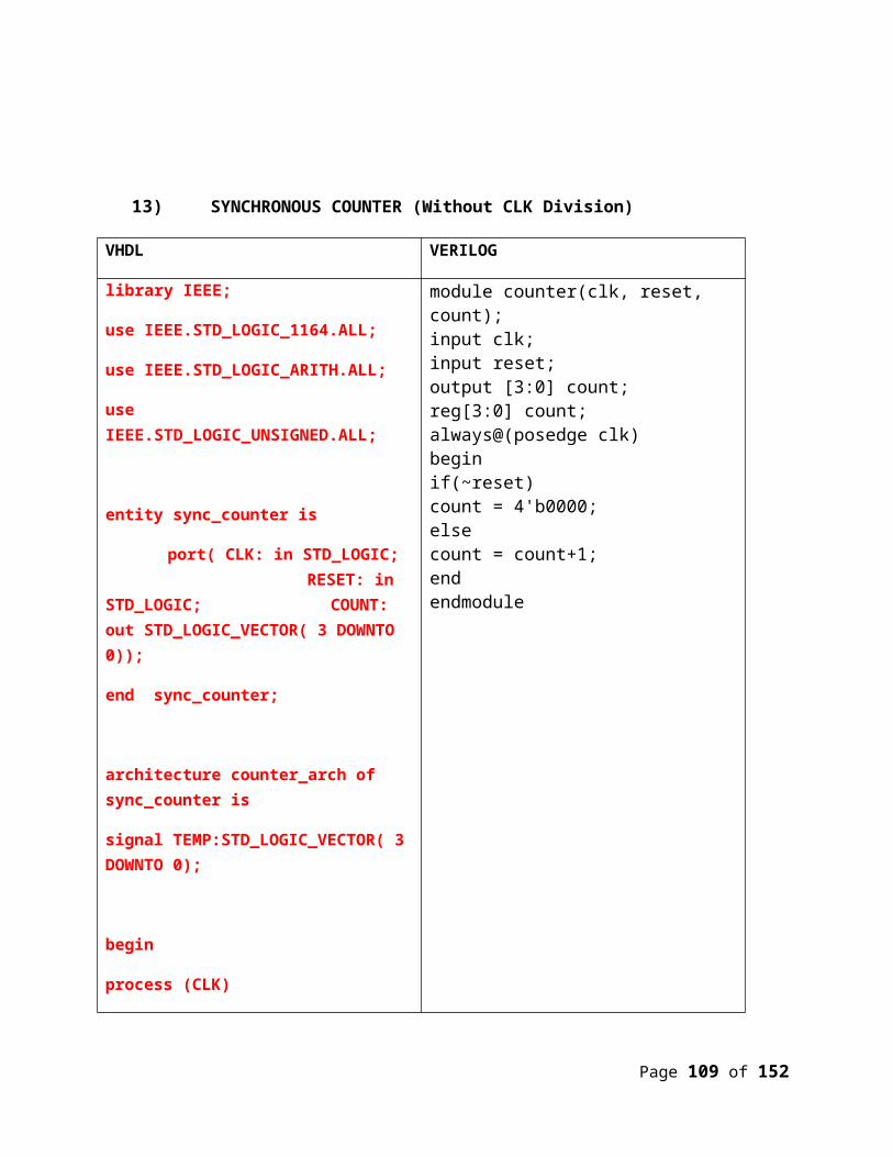
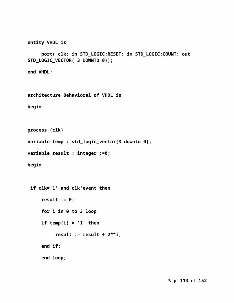
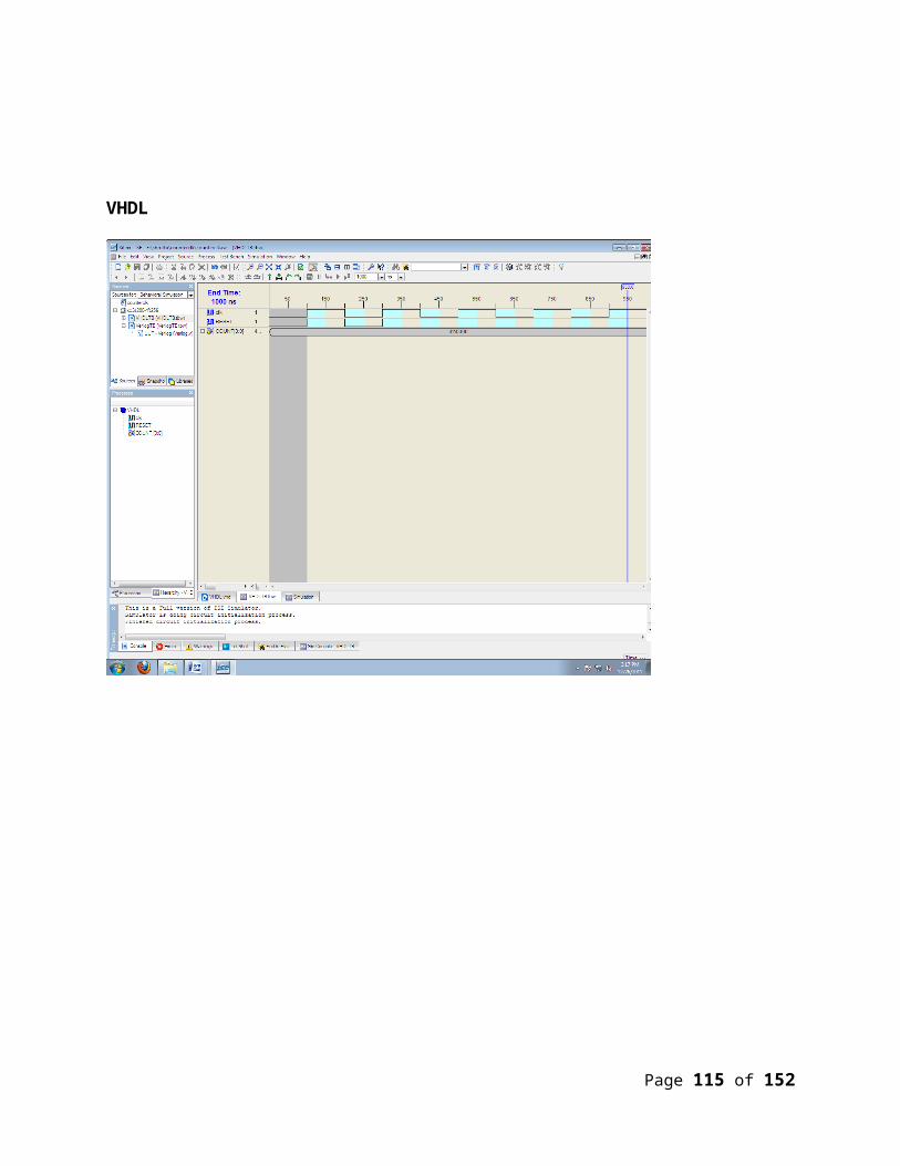
13) SYNCHRONOUS COUNTER (Without CLK Division)
VHDL VERILOG
library IEEE;
use IEEE.STD_LOGIC_1164.ALL;
use IEEE.STD_LOGIC_ARITH.ALL;
use IEEE.STD_LOGIC_UNSIGNED.ALL;
entity sync_counter is
port( CLK: in STD_LOGIC; RESET: in
STD_LOGIC; COUNT: out STD_LOGIC_VECTOR( 3 DOWNTO 0));
end sync_counter;
architecture counter_arch of sync_counter is
signal TEMP:STD_LOGIC_VECTOR( 3 DOWNTO 0);
begin
process (CLK)
begin
if CLK='1' and CLK'event then
module counter(clk, reset, count);input clk;input reset;output [3:0] count;reg[3:0] count;always@(posedge clk)beginif(~reset)count = 4'b0000;elsecount = count+1;endendmodule
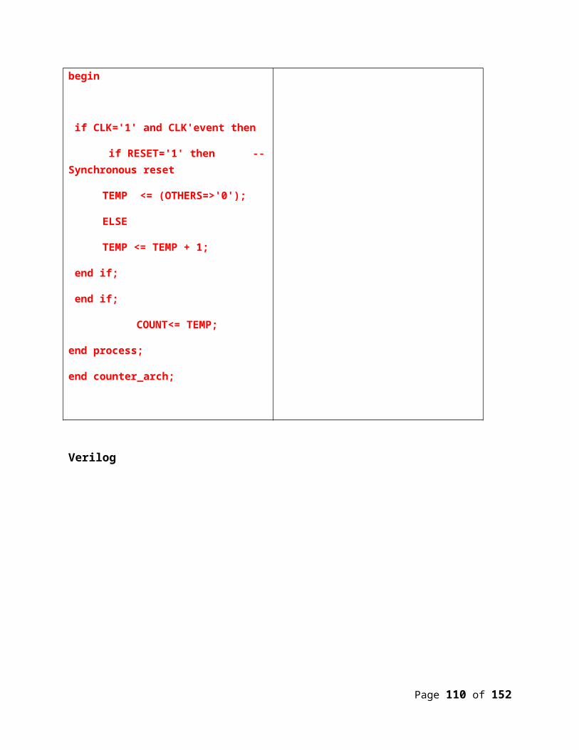
Page 95 of 132
if RESET='1' then --Synchronous reset
TEMP <= (OTHERS=>'0');
ELSE
TEMP <= TEMP + 1;
end if;
end if;
COUNT<= TEMP;
end process;
end counter_arch;
Verilog
Page 96 of 132
library IEEE;
use IEEE.STD_LOGIC_1164.ALL;
use IEEE.STD_LOGIC_ARITH.ALL;
use IEEE.STD_LOGIC_UNSIGNED.ALL;
---- Uncomment the following library declaration if instantiating
---- any Xilinx primitives in this code.
--library UNISIM;
--use UNISIM.VComponents.all;
Page 97 of 132
entity VHDL is
port( clk: in STD_LOGIC;RESET: in STD_LOGIC;COUNT: out STD_LOGIC_VECTOR( 3 DOWNTO 0));
end VHDL;
architecture Behavioral of VHDL is
begin
process (clk)
variable temp : std_logic_vector(3 downto 0);
variable result : integer :=0;
begin
if clk='1' and clk'event then
result := 0;
for i in 0 to 3 loop
if temp(i) = '1' then
result := result + 2**i;
end if;
end loop;
result := result + 1;
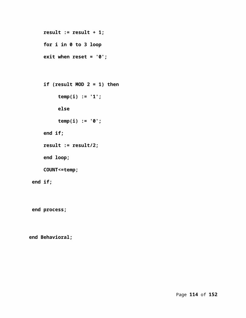
Page 98 of 132
for i in 0 to 3 loop
exit when reset = '0';
if (result MOD 2 = 1) then
temp(i) := '1';
else
temp(i) := '0';
end if;
result := result/2;
end loop;
COUNT<=temp;
end if;
end process;
end Behavioral;
VHDL
Page 99 of 132
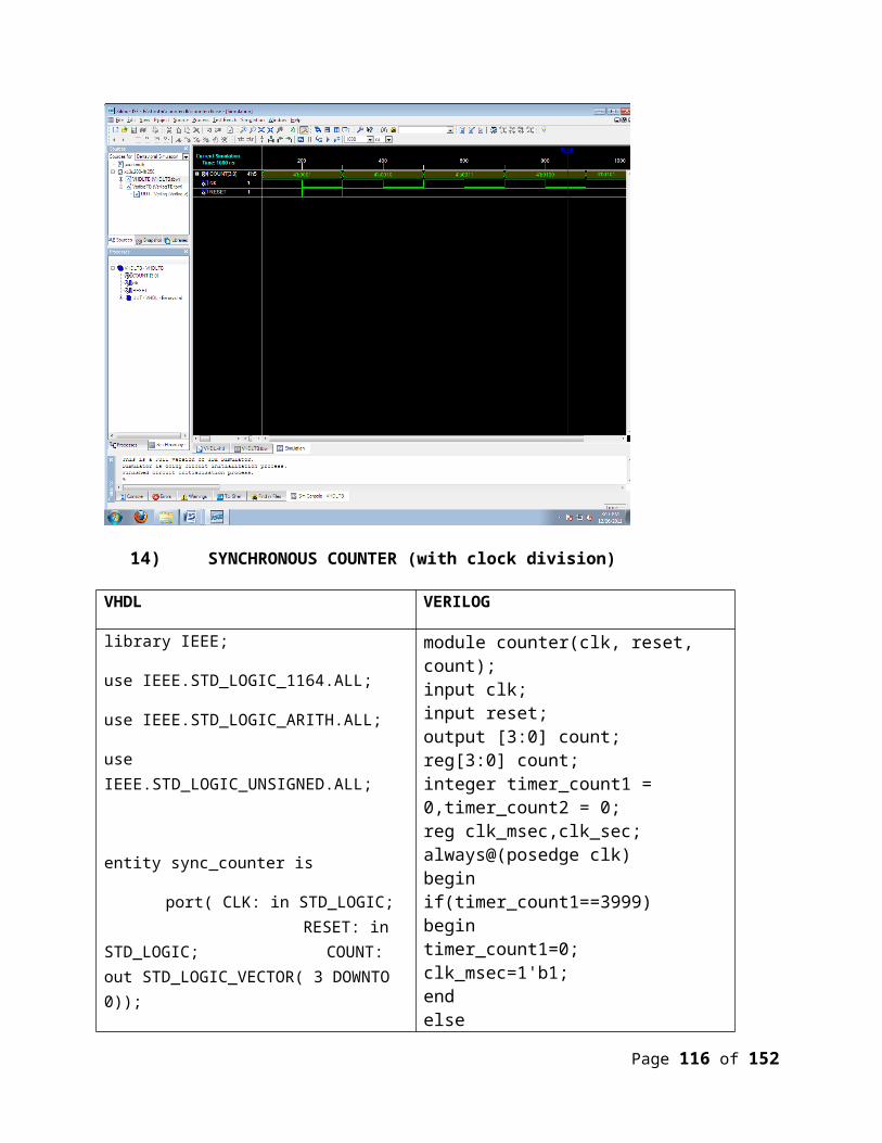
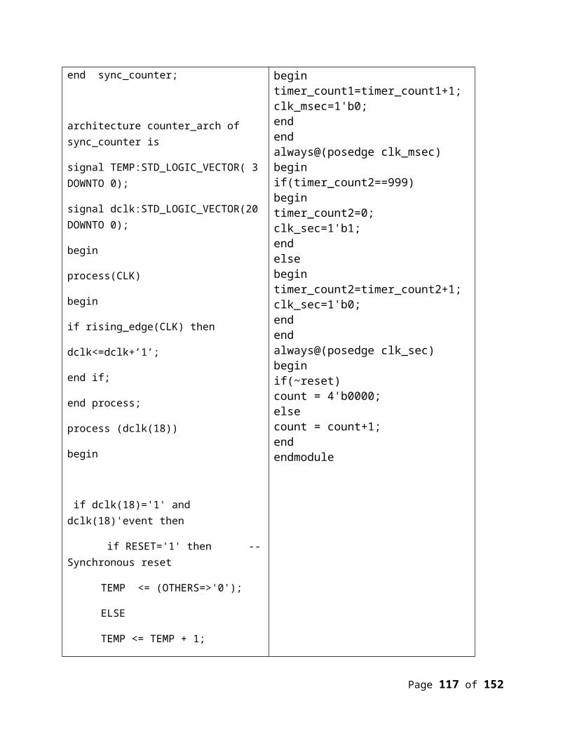
14) SYNCHRONOUS COUNTER (with clock division)
Page 100 of 132
VHDL VERILOG
library IEEE;
use IEEE.STD_LOGIC_1164.ALL;
use IEEE.STD_LOGIC_ARITH.ALL;
use IEEE.STD_LOGIC_UNSIGNED.ALL;
entity sync_counter is
port( CLK: in STD_LOGIC; RESET: in
STD_LOGIC; COUNT: out STD_LOGIC_VECTOR( 3 DOWNTO 0));
end sync_counter;
architecture counter_arch of sync_counter is
signal TEMP:STD_LOGIC_VECTOR( 3 DOWNTO 0);
signal dclk:STD_LOGIC_VECTOR(20 DOWNTO 0);
begin
process(CLK)
begin
if rising_edge(CLK) then
dclk<=dclk+’1’;
end if;
end process;
process (dclk(18))
begin
module counter(clk, reset, count);input clk;input reset;output [3:0] count;reg[3:0] count;integer timer_count1 = 0,timer_count2 = 0;reg clk_msec,clk_sec;always@(posedge clk)beginif(timer_count1==3999)begintimer_count1=0;clk_msec=1'b1;endelsebegintimer_count1=timer_count1+1;clk_msec=1'b0;endendalways@(posedge clk_msec)beginif(timer_count2==999)begintimer_count2=0;clk_sec=1'b1;endelsebegintimer_count2=timer_count2+1;clk_sec=1'b0;endendalways@(posedge clk_sec)beginif(~reset)count = 4'b0000;elsecount = count+1;endendmodule
Page 101 of 132
if dclk(18)='1' and dclk(18)'event then
if RESET='1' then --Synchronous reset
TEMP <= (OTHERS=>'0');
ELSE
TEMP <= TEMP + 1;
end if;
end if;
COUNT<= TEMP;
end process;
end counter_arch;
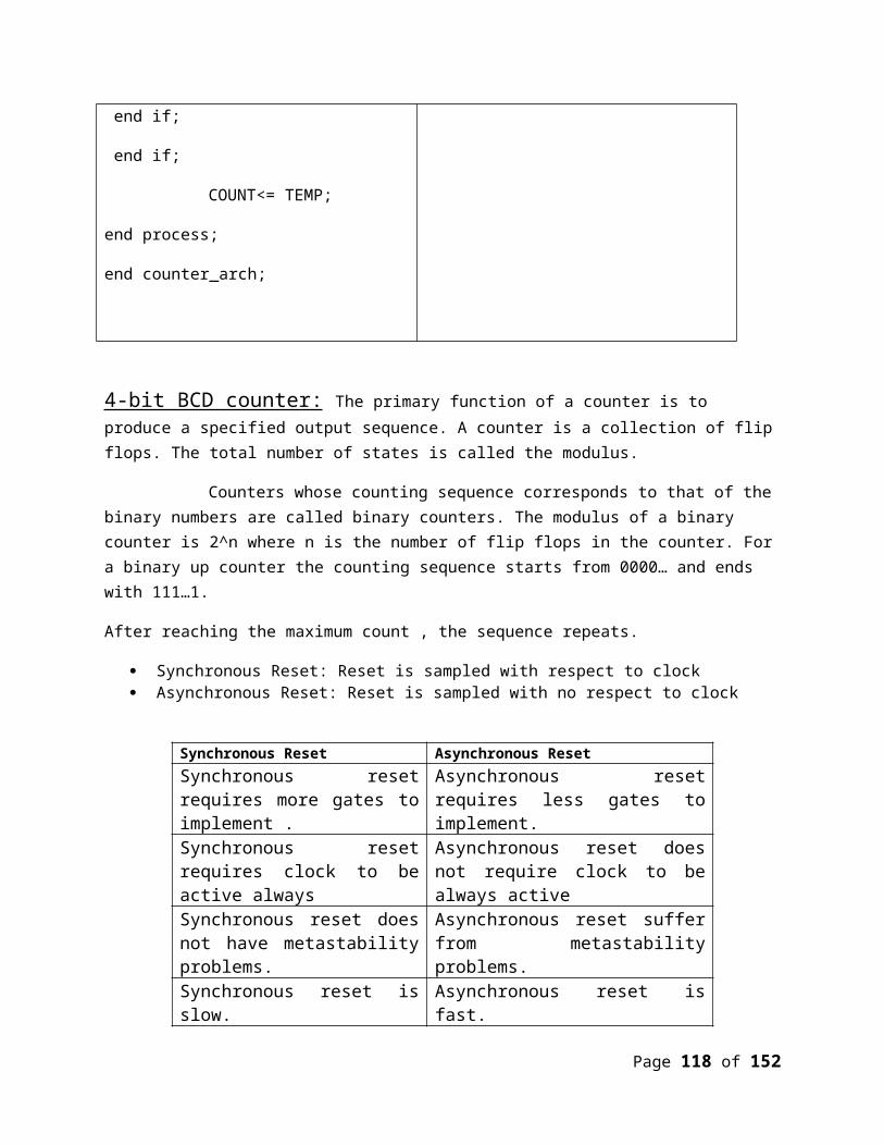
4-bit BCD counter: The primary function of a counter is to produce a specified output sequence. A counter is a collection of flip flops. The total number of states is called the modulus.
Counters whose counting sequence corresponds to that of the binary numbers are called binary counters. The modulus of a binary counter is 2^n where n is the number of flip flops in the counter. For a binary up counter the counting sequence starts from 0000… and ends with 111…1.
After reaching the maximum count , the sequence repeats.
Synchronous Reset: Reset is sampled with respect to clock Asynchronous Reset: Reset is sampled with no respect to clock
Synchronous Reset Asynchronous Reset
Synchronous reset requires more gates to implement .
Asynchronous reset requires less gates to implement.
Synchronous reset requires clock to be active always
Asynchronous reset does not require clock to be always active
Synchronous reset does not have metastability problems.
Asynchronous reset suffer from metastability problems.
Synchronous reset is slow. Asynchronous reset is fast.
Page 102 of 132
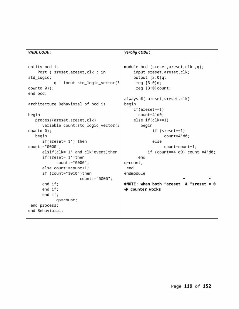
VHDL CODE : Verolig CODE :
entity bcd is Port ( sreset,areset,clk : in std_logic; q : inout std_logic_vector(3 downto 0));end bcd;
architecture Behavioral of bcd is
begin process(areset,sreset,clk)
variable count:std_logic_vector(3 downto 0); begin
if(areset='1') then count:="0000";elsif(clk='1' and clk'event)thenif(sreset='1')then count:="0000";else count:=count+1;if (count="1010")then
count:="0000"; end if;end if;end if;
q<=count; end process;end Behavioral;
module bcd (sreset,areset,clk ,q); input sreset,areset,clk; output [3:0]q; reg [3:0]q; reg [3:0]count;
always @( areset,sreset,clk)begin if(areset==1)
count=4'd0; else if(clk==1) begin if (sreset==1) count=4'd0; else count=count+1;
if (count==4'd9) count =4'd0; endq=count; endendmodule
#NOTE: when both “areset” & “sreset”= 0 counter works
Verilog
Page 103 of 132
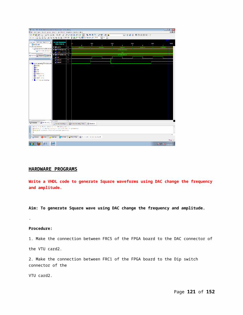
HARDWARE PROGRAMS
Page 104 of 132
Write a VHDL code to generate Square waveforms using DAC change the frequency and amplitude.
Aim: To generate Square wave using DAC change the frequency and amplitude.
.
Procedure:
1. Make the connection between FRC5 of the FPGA board to the DAC connector of
the VTU card2.
2. Make the connection between FRC1 of the FPGA board to the Dip switch connector of the
VTU card2.
3. Connect the downloading cable and power supply to the FPGA board.
4. Then open the Xilinx iMPACT software (refer ISE flow) select the slave serial mode and
select the respective BIT file and click program.
5. Make the reset switch on (active low) and analyze the data.
VHDL CODING
library IEEE;
use IEEE.STD_LOGIC_1164.ALL;
use IEEE.STD_LOGIC_ARITH.ALL;
use IEEE.STD_LOGIC_UNSIGNED.ALL;
entity square_wave is
Port ( clk : in std_logic;
rst : in std_logic;
dac_out : out std_logic_vector(0 to 7));
end square_wave;
architecture Behavioral of square_wave is
signal temp : std_logic_vector(3 downto 0);--Clk division clk/16---
signal counter : std_logic_vector(0 to 7);---- 8 Bit Counter----
Page 105 of 132
begin
process(clk)
begin
if rising_edge(clk) then
temp <= temp + '1' ;
end if;
end process;
process(temp(3))
begin
if rst='1' then
counter <= "00000000";
elsif rising_edge(temp(3)) then
if counter<255 then
counter <= counter + 1 ;
dac_out <="00000000";
else
counter <= counter-1;
dac_out <="11111111";
end if;
end if;
end process;
end Behavioral;
UCF file(User constraint File)
NET "clk" LOC = "p52" ;
NET "dac_out<0>" LOC = "p21" ;
NET "dac_out<1>" LOC = "p18" ;
NET "dac_out<2>" LOC = "p17" ;
Page 106 of 132
NET "dac_out<3>" LOC = "p15" ;
NET "dac_out<4>" LOC = "p14" ;
NET "dac_out<5>" LOC = "p13" ;
NET "dac_out<6>" LOC = "p12" ;
NET "dac_out<7>" LOC = "p11" ;
NET "rst" LOC = "p74" ;
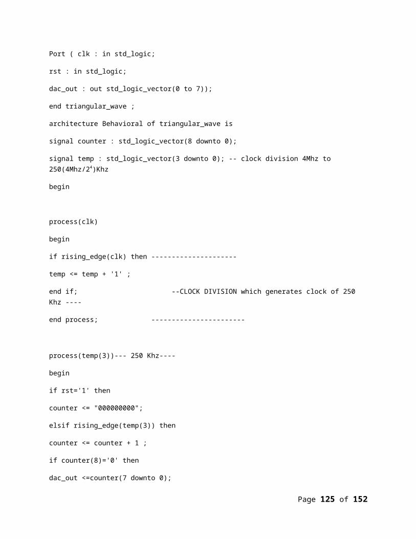
3c. write a VHDL code to generate Triangular waveforms using DAC change the frequency and amplitude.
Aim: To generate Triangular wave using DAC change the frequency and amplitude.
.
Procedure:
1. Make the connection between FRC5 of the FPGA board to the DAC connector of
the VTU card2.
2. Make the connection between FRC1 of the FPGA board to the Dip switch connector of the
VTU card2.
3. Connect the downloading cable and power supply to the FPGA board.
4. Then open the Xilinx iMPACT software (refer ISE flow) select the slave serial mode and
select the respective BIT file and click program.
5. Make the reset switch on (active low) and analyze the data.
VHDL CODING
library IEEE;
use IEEE.STD_LOGIC_1164.ALL;
use IEEE.STD_LOGIC_ARITH.ALL;
use IEEE.STD_LOGIC_UNSIGNED.ALL;
entity triangular_wave is
Page 107 of 132
Port ( clk : in std_logic;
rst : in std_logic;
dac_out : out std_logic_vector(0 to 7));
end triangular_wave ;
architecture Behavioral of triangular_wave is
signal counter : std_logic_vector(8 downto 0);
signal temp : std_logic_vector(3 downto 0); -- clock division 4Mhz to 250(4Mhz/24)Khz
begin
process(clk)
begin
if rising_edge(clk) then ---------------------
temp <= temp + '1' ;
end if; --CLOCK DIVISION which generates clock of 250 Khz ----
end process; -----------------------
process(temp(3))--- 250 Khz----
begin
if rst='1' then
counter <= "000000000";
elsif rising_edge(temp(3)) then
counter <= counter + 1 ;
if counter(8)='0' then
dac_out <=counter(7 downto 0);
else
dac_out <=not(counter(7 downto 0));
end if;
end if;
Page 108 of 132
end process;
end Behavioral;
UCF file(User constraint File)
NET "clk" LOC = "p52" ;
NET "dac_out<0>" LOC = "p21" ;
NET "dac_out<1>" LOC = "p18" ;
NET "dac_out<2>" LOC = "p17" ;
NET "dac_out<3>" LOC = "p15" ;
NET "dac_out<4>" LOC = "p14" ;
NET "dac_out<5>" LOC = "p13" ;
NET "dac_out<6>" LOC = "p12" ;
NET "dac_out<7>" LOC = "p1" ;
NET "rst" LOC = "p74" ;
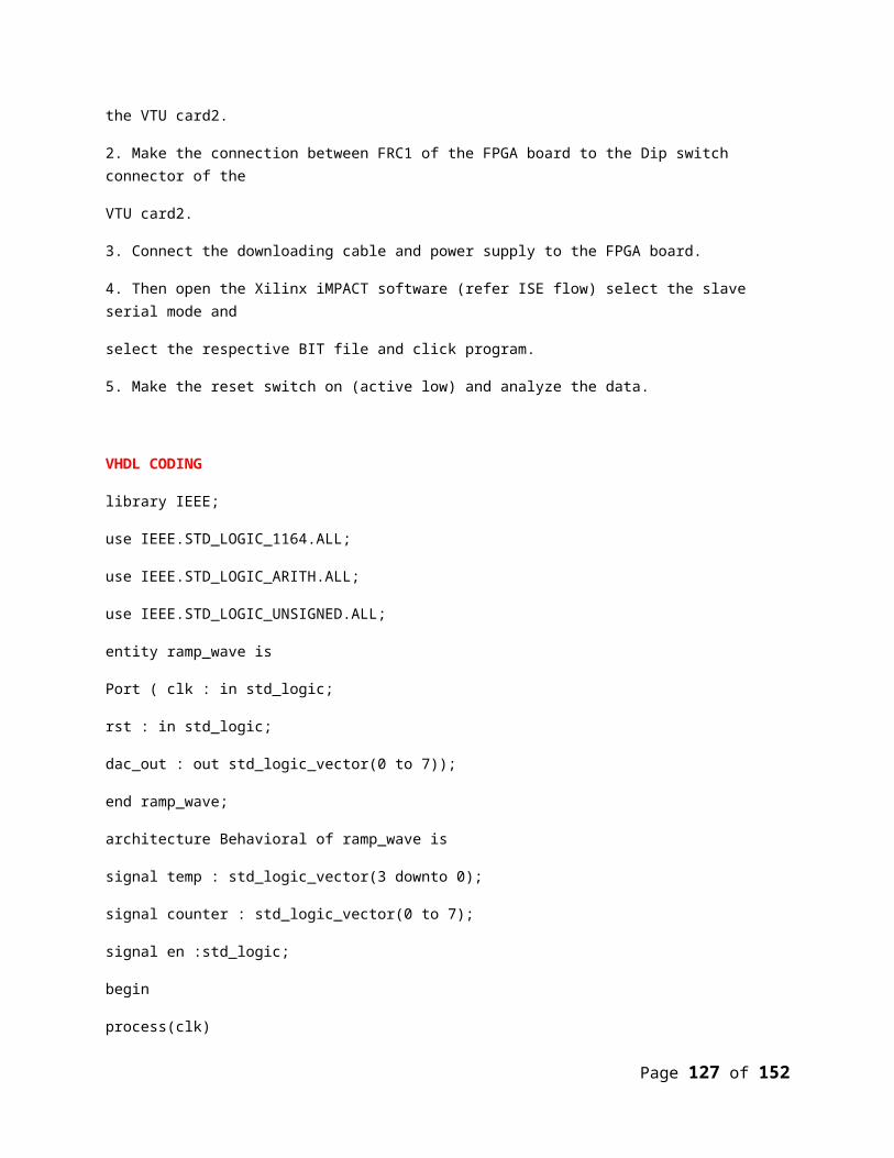
4d. Write a VHDL code to generate Ramp waveforms using DAC change the frequency and amplitude.
Aim: To generate Ramp wave using DAC change the frequency and amplitude.
.
Procedure:
1. Make the connection between FRC5 of the FPGA board to the DAC connector of
the VTU card2.
2. Make the connection between FRC1 of the FPGA board to the Dip switch connector of the
VTU card2.
3. Connect the downloading cable and power supply to the FPGA board.
4. Then open the Xilinx iMPACT software (refer ISE flow) select the slave serial mode and
select the respective BIT file and click program.
Page 109 of 132
5. Make the reset switch on (active low) and analyze the data.
VHDL CODING
library IEEE;
use IEEE.STD_LOGIC_1164.ALL;
use IEEE.STD_LOGIC_ARITH.ALL;
use IEEE.STD_LOGIC_UNSIGNED.ALL;
entity ramp_wave is
Port ( clk : in std_logic;
rst : in std_logic;
dac_out : out std_logic_vector(0 to 7));
end ramp_wave;
architecture Behavioral of ramp_wave is
signal temp : std_logic_vector(3 downto 0);
signal counter : std_logic_vector(0 to 7);
signal en :std_logic;
begin
process(clk)
begin
if rising_edge(clk) then
temp <= temp + '1' ;
end if;
end process;
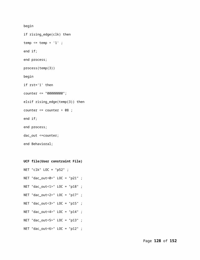
process(temp(3))
begin
if rst='1' then
counter <= "00000000";
elsif rising_edge(temp(3)) then
Page 110 of 132
counter <= counter + 08 ;
end if;
end process;
dac_out <=counter;
end Behavioral;
UCF file(User constraint File)
NET "clk" LOC = "p52" ;
NET "dac_out<0>" LOC = "p21" ;
NET "dac_out<1>" LOC = "p18" ;
NET "dac_out<2>" LOC = "p17" ;
NET "dac_out<3>" LOC = "p15" ;
NET "dac_out<4>" LOC = "p14" ;
NET "dac_out<5>" LOC = "p13" ;
NET "dac_out<6>" LOC = "p12" ;
NET "dac_out<7>" LOC = "p1" ;
NET "rst" LOC = "p74" ;
3e. Write a VHDL code to generate Sawtooth waveforms using DAC change the frequency and amplitude.
Aim: To generate Sawtooth wave using DAC change the frequency and amplitude.
Procedure:
1. Make the connection between FRC5 of the FPGA board to the DAC connector of
the VTU card2.
2. Make the connection between FRC1 of the FPGA board to the Dip switch connector of the
VTU card2.
Page 111 of 132
3. Connect the downloading cable and power supply to the FPGA board.
4. Then open the Xilinx iMPACT software (refer ISE flow) select the slave serial mode and
select the respective BIT file and click program.
5. Make the reset switch on (active low) and analyze the data.
VHDL CODING
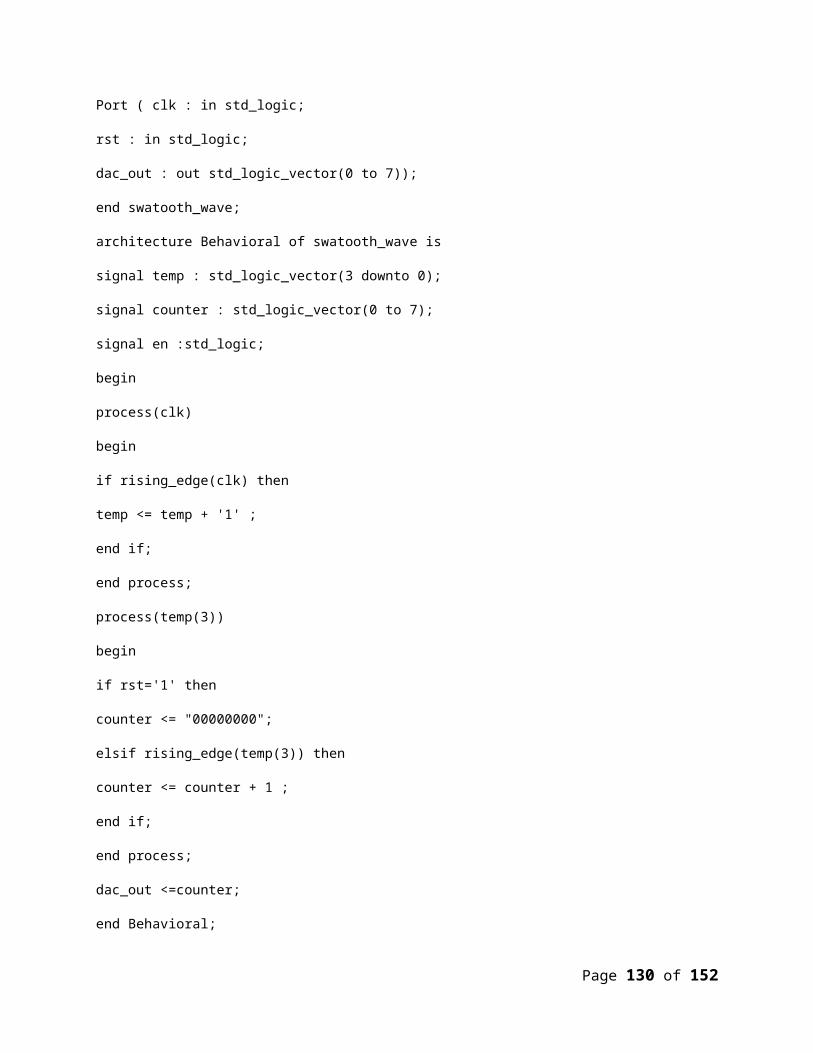
library IEEE;
use IEEE.STD_LOGIC_1164.ALL;
use IEEE.STD_LOGIC_ARITH.ALL;
use IEEE.STD_LOGIC_UNSIGNED.ALL;
entity swatooth_wave is
Port ( clk : in std_logic;
rst : in std_logic;
dac_out : out std_logic_vector(0 to 7));
end swatooth_wave;
architecture Behavioral of swatooth_wave is
signal temp : std_logic_vector(3 downto 0);
signal counter : std_logic_vector(0 to 7);
signal en :std_logic;
begin
process(clk)
begin
if rising_edge(clk) then
temp <= temp + '1' ;
end if;
end process;
process(temp(3))
begin
Page 112 of 132
if rst='1' then
counter <= "00000000";
elsif rising_edge(temp(3)) then
counter <= counter + 1 ;
end if;
end process;
dac_out <=counter;
end Behavioral;
UCF file(User constraint File)
NET "clk" LOC = "p52" ;
NET "dac_out<0>" LOC = "p21" ;
NET "dac_out<1>" LOC = "p18" ;
NET "dac_out<2>" LOC = "p17" ;
NET "dac_out<3>" LOC = "p15" ;
NET "dac_out<4>" LOC = "p14" ;
NET "dac_out<5>" LOC = "p13" ;
NET "dac_out<6>" LOC = "p12" ;
NET "dac_out<7>" LOC = "p1" ;
NET "rst" LOC = "p74" ;
4. Write a VHDL code to control external lights using relays.
Aim: To control external lights using relays.
Procedure:
1. Make the connection between FRC9 of the FPGA board to the External light
connector of the VTU card2.
2. Make the connection between FRC1 of the FPGA board to the Dip switch connector
of the VTU card2.
Page 113 of 132
3. Connect the downloading cable and power supply to the FPGA board.
4. Then open the Xilinx iMPACT software (refer ISE flow) select the slave serial mode
and select the respective BIT file and click program.
5. Make the reset switch on (active low) and analyze the data.
VHDL CODING
library IEEE;
use IEEE.STD_LOGIC_1164.ALL;
use IEEE.STD_LOGIC_ARITH.ALL;
use IEEE.STD_LOGIC_UNSIGNED.ALL;
entity extlight is
Port ( cntrl1,cntrl2 : in std_logic;
light : out std_logic);
end extlight;
architecture Behavioral of extlight is
begin
light<= cntrl1 OR cntrl2 ;
end Behavioral;
UCF file(User constraint)
NET "cntrl1" LOC = "P74";
NET "cntrl2" LOC = "P76";
NET "light" LOC = "P5";
5. Write a VHDL code to control speed, direction of DC motor.
Aim: To control Speed and Direction of DC motor.
Procedure:
Page 114 of 132
1. Make the connection between FRC9 of the FPGA board to the DC motor connector of the VTU card2.
2. Make the connection between FRC7 of the FPGA board to the Keyboard connector of the VTU card2.
3. Make the connection between FRC1 of the FPGA board to the Dip switch connector of the VTU card2.
4. Connect the downloading cable and power supply to the FPGA board.
5. Then open the Xilinx iMPACT software (refer ISE flow) select the slave serial mode and select the respective BIT file and click program.
6. Make the reset switch on (active low).
7. Press the HEX keys and analyze the speed changes.
VHDL CODING
Library IEEE;
use IEEE.std_logic_1164.all;
use IEEE.STD_LOGIC_UNSIGNED.all;
Library UNISIM;
use UNISIM.vcomponents.all;
entity dcmotor is
generic(bits : integer := 8 ); -- number of bits used for duty cycle.
-- Also determines pwm period.
port ( CLK: in STD_LOGIC; -- 4 MHz clock
RESET,DIR: in STD_LOGIC; -- dircntr
pwm : out std_logic_VECTOR(1 DOWNTO 0);
rly: out std_logic;
ROW: in STD_LOGIC_VECTOR(0 to 3) ); -- this are the row lines
end dcmotor;
architecture dcmotor1 of dcmotor is
signal counter : std_logic_vector(bits - 1 downto 0):="11111110";
Page 115 of 132
signal DIV_REG: STD_LOGIC_VECTOR (16 downto 0); -- clock divide register
signal DCLK,DDCLK,datain,tick: STD_LOGIC; -- this has the divided clock.
signal duty_cycle: integer range 0 to 255;
signal ROW1 : STD_LOGIC_VECTOR(0 to 3); -- this are the row lines
begin
-- select the appropriate lines for setting frequency
CLK_DIV: process (CLK, DIV_REG) -- clock divider
begin
if (CLK'event and CLK='1') then
DIV_REG <= DIV_REG + 1;
end if;
end process;
DDCLK<=DIV_REG(12);
---------------------------- END OF CLOCK DIVIDER -------------------------------------------------
tick <= row(0) and row(1) and row(2) and row(3);
process(tick)
begin
if falling_edge(tick) then
case row is
when "1110" => duty_cycle <= 255 ; --motor speed 1
when "1101" => duty_cycle <= 200 ; --motor speed 2
when "1011" => duty_cycle <= 150 ; --motor speed 3
when "0111" => duty_cycle <= 100 ; --motor speed 4
when others => duty_cycle <= 100;
end case;
end if;
Page 116 of 132
end process;
process(DDCLK, reset)
begin
if reset = '0' then
counter <= (others => '0');
PWM<="01";
elsif (DDCLK'event and DDCLK = '1') then
counter <= counter + 1;
if counter >= duty_cycle then
pwm(1) <= '0';
else
pwm(1) <= '1';
end if; end if;
end process;
rly<=DIR --motor direction control
end dcmotor1;
UCF file(User constraint File)
NET "CLK" LOC = "p52" ;
NET IR LOC = 76; //FRC1 – pin 2 – for direction – toggle dip switch to check direction of motion of the DC motor
NET "pwm<0>" LOC = "p4" ;
NET "pwm<1>" LOC = "p141" ;
NET "RESET" LOC = "p74" ; //FRC1 – pin1 – for reset – kept low in dip switch
NET "rly" LOC = "p44" ;
NET "ROW<0>" LOC = "p69" ; //the below 4 are FRC7 – keys – pins 1,2,3,4- for varying speeds
Page 117 of 132
NET "ROW<1>" LOC = "p63" ;
NET "ROW<2>" LOC = "p59" ;
NET "ROW<3>" LOC = "p57" ;
5. Write a VHDL code to control speed, direction of Stepper motor.
Aim: To control Speed and Direction of Stepper motor.
Procedure:
1. Make the connection between FRC9 of the FPGA board to the Stepper motor connector of the VTU card2.
2. Make the connection between FRC7 of the FPGA board to the Keyboard connector of the VTU card2.
3. Make the connection between FRC1 of the FPGA board to the Dip switch connector of the VTU card2.
4. Connect the downloading cable and power supply to the FPGA board.
5. Then open the Xilinx iMPACT software (refer ISE flow) select the slave serial mode and select the respective BIT file and click program.
6. Make the reset switch on (active low).
7. Press the HEX keys and analyze the speed changes.
VHDL CODING
library IEEE;
use IEEE.STD_LOGIC_1164.ALL;
use IEEE.STD_LOGIC_ARITH.ALL;
use IEEE.STD_LOGIC_UNSIGNED.ALL;
.entity STEPPERnew is
Port ( dout : out std_logic_vector(3 downto 0);
clk,reset: in std_logic;
row:in std_logic_vector(1 downto 0);
dir:in std_logic);
Page 118 of 132
end STEPPERnew;
architecture Behavioral of STEPPERnew is
signal clk_div : std_logic_vector(25 downto 0);
signal clk_int: std_logic;
signal shift_reg : std_logic_vector(3 downto 0);
begin
process(clk)
begin
if rising_edge (clk) then
clk_div <= clk_div + '1';
end if;
end process;
clk_int<=clk_div(21) when row="00"else
clk_div(19) when row="01"else
clk_div(17) when row="10"else
clk_div(15) ;
process(reset,clk_int,dir)
begin
if reset='0' then
shift_reg <= "1001";
elsif rising_edge(clk_int) then
if dir='0' then
shift_reg <= shift_reg(0) & shift_reg(3 downto 1);
else
shift_reg<=shift_reg(2 downto 0) & shift_reg(3);
end if;
Page 119 of 132
end if;
end process;
dout <= shift_reg;
end Behavioral;
UCF file(User constraint File)
NET "clk" LOC = "p52" ;
NET "dir" LOC = "p76" ; //FRC1 – pin 2 – for direction – dip switch
NET "dout<0>" LOC = "p141" ;
NET "dout<1>" LOC = "p2" ;
NET "dout<2>" LOC = "p4" ;
NET "dout<3>" LOC = "p5" ;
NET "reset" LOC = "p74" ; //FRC1 – pin 1 – for reset – dip switch
NET "row<0>" LOC = "p77" ; //FRC1 – pins 3 & 4 – for speed control
Note here;
For 00, 01, 10 & 11 in dip switch, we can observe varying speeds
NET "row<1>" LOC = "p79" ;
Page 120 of 132
INTERFACING EXPERIMENTS
PATTERN GENERATOR AND LOGIC ANALYSER
1) Introduction
Debugging today’s digital systems is tougher than ever. You need highperformance, reliable tools to help you overcome the difficult engineeringchallenges you face. The logic analysis systems help you to solve toughdebug problems, minimize your project risk, and get your leading-edgeproducts to market faster. These systems provide excellent performanceand accurate, reliable measurements priced to match your budget. And,because you can t measure what you can t probe, we have usedinnovative probing technologies so you can access critical signals in yourdesigns. These analyzers include an intuitive Windows graphical userinterface and straightforward triggering capability so you spend more timeon design and debug and less time learning how to use them.Generating high quality patterns has become an engineering specialty initself, particularly in the face of new communication technologies thatdemand precise testing to exacting standards. With the help of integrated
Page 121 of 132
CM 640 L/A cum P/G shows what advanced signal engineering is capableof creating.
2) FEATURES OF THE CM 640 PATTERN GENERATOR CUM LOGICANALYZER:
Specifications:
On board power supplyIn built Crystal Oscillator (4 HZ)Power Adapter and Downloading cablesIn built power regulatorsPower indicator LEDOn board Separate FRC connectors for L/A and P/G
3) PRECAUTIONS:
Connect Proper download cable (Serial port) before applying the power.Do not Remove/Place Cable with power connected to instrument.Connect only the Power adopter, which is supplied along with theinstrument.Ensure the power supply is stable and monotonous before connectingthe Serial port cable.Ensure that the location constraints are consistent with the hardware.
4) Method of Using CM 640.
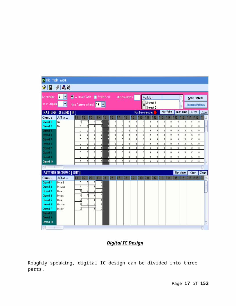
The integrated CMD 640 has on one side pattern generator otherside logic analyzer and can be used as stand alone pattern generator andstand alone logic analyzer.
The connections can be made to L/A or P/G through FRC connectors fixedon both sides, and L/A has 32 channels and P/G has 32 channels andeach FRC connector has 8 I/O pins and Vcc and Gnd. The first pin ismarked by the arrow symbol on the FRC connector.
The GUI of CM640 is having Pattern generator on upper part named aspattern to send (in), and below Logic analyzer part named as PatternReceived (out).
Select a new file on tool bar.
Browse for the UCF and provide i/p and o/p details.
Page 122 of 132
The number of inputs and outputs to be selected.Check in the tool bar, in the tools options select the proper COM port.(9600 baud rate).
Give the input by clicking on the corresponding input lines by making theline high or low and decide the data depth (no of patterns).
Select the mode continuous. In case of clock select the clock.Send patterns then simultaneously the output will be displayed on the L/Aside, simultaneously the Truth table also created and can be viewed byclicking the truth table button.
The CM640 has inbuilt Clock of frequency 4 Hz to view outputs,no need to divide the clock in the design if the board clock is isolated andthe clock option of CM640 is used. To make use of clk of the CM640connect next pin after assignments of all the inputs, the very next pin isassigned to clk of the FRC of P/G side.
Pin details of interfacing boards
GPIO CARD-1KEY PAD LCDDIP
Page 123 of 132
Page 124 of 132
Page 125 of 132
Page 126 of 132
Page 127 of 132
Pin details of mother boards
Page 128 of 132
Page 129 of 132
VIVA QUESTIONS
1. What type of language is VHDL?2. What is the basic building unit of a VHDL design?3. What do all VHDL designs begin with?4. Which block describes a design's interface?5. Which block describes a design's behavior?6. What is the difference between simulation and synthesis?7. Which data type defines a single logic signal?8. Which data type describes a bus?9. What two ways can a vector's range be described?10. What are the IEEE STD_LOGIC_1164 data types for single logic signals and buses?11. Why is it desirable to use IEEE STD_LOGIC_1164 data typing?12. What are the only two values for a Boolean type?13. What are the numerical data types?14. What is SUBTYPING used for?15. What type is use to create a user data type?16. What reserved word is used to declare a user data type?17. Create the use data type DAYS and assign it the values: MON, TUE, WED, THU, FRI,SAT and SUN.18. Which data type is used for a string of ASCII characters?19. Which data type includes time units as values?20 Create the entity block for a three input XOR gate.21. Which symbol is used to end all VHDL statements?22. What part of a port declaration defines signals in or out direction?23. Which VHDL construct is used to define a literal constant in an entity block?24. Create the integer constant included in an entity block called BUS_SIZE and assignit a value of 32.25. Which symbols are used as an assignment operator to assign a literal to an identifiername?26. What are the two primary ways to describe a logic circuits function within anarchitecture block?27. Create the architecture block for the 3-input XOR gate of question 21.28. Which symbols are used to assign an expression's result to an output interfacesignal?29. What are the rules used to define an identifier name?30. What symbols define a comment line?
Page 130 of 132
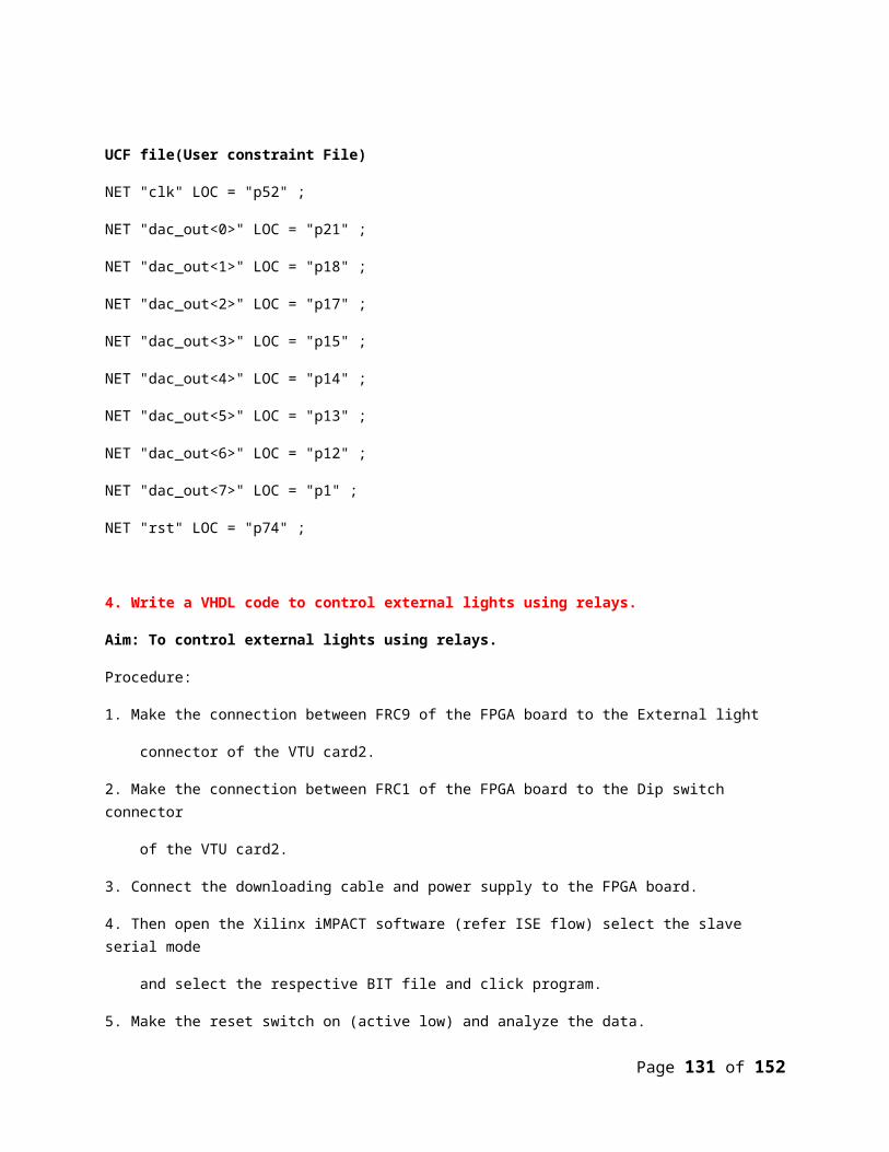
31. Write the statements that will allow a design to access all the contents of the IEEE ARITH.32. Make the delay in question 33 transport rather than inertial.33. How does a transport delay differ from an inertial delay?34. What is the purpose of a SIGNAL declaration?35. Where are SIGNAL declarations placed in the design?36. Write an assignment statement that assigns the contents of s(5) to t(2).37.What is the purpose of a process' sensitivity list?38 Under what conditions is a process run?39 What is an EVENT?40 What is the difference between event and non-event driven process execution?41. Write a process block that keeps a running tally of each time an interrupt (INT)signal is asserted high.42. Which symbols are used to differentiate between logic 1 and an integer 1?43. What are the results of using CLK'event as a condition in the if statement of theDEF example?44.In an if..then..else construct, which statements are executed if the condition isTRUE and which if it is FALSE?45. What reserved word is used to nest if..then..else statements?46. Write the process block that separately tallies positive and negative transitions of thesignal TIME_OUT.47. What is the purpose of a for loop?48. What are the requirements for a for loop?49. Write a process block that uses a for loop to set a zero flag high if all the bits in asixteen (16) bit word are low (zero).50. Write is the general rule for component declarations?51. What is meant by instantiating a component?52. How do signal declarations differ from port interface declarations?53. What is the prime use of signals?54. How many parameters can be passed into a function?55. How many results can be returned from a function?56. Write a function that returns the sum of two 8-bit words.57. How are functions called?58. How do procedures differ from functions?59. Which standard library does not require a library or use statement?60. What is a PACKAGE?61. When is a PACKAGE BODY used?62. What is the name of the library used by the current design to store compiled results?
Page 131 of 132
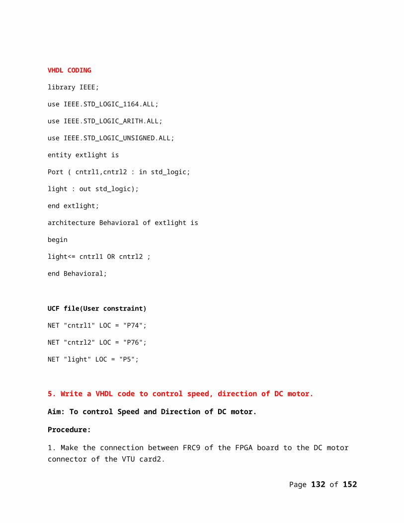
63. Which standard library is used to access the keyboard and monitor screen?
***********************************************************************
Page 132 of 132
Related Documents


![Blessing Manual[1] Copy](https://static.cupdf.com/doc/110x72/577cd1341a28ab9e7893dcc4/blessing-manual1-copy.jpg)