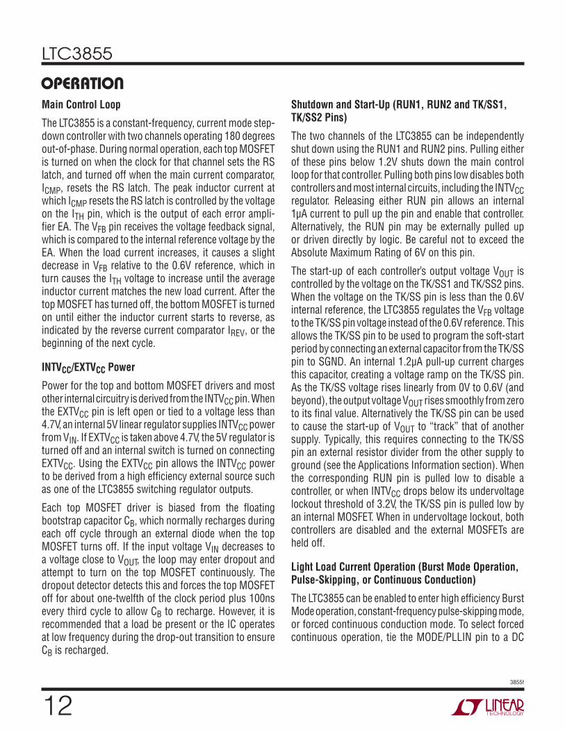
LTC3855 3855f TYPICAL APPLICATION DESCRIPTION Dual, Multiphase Synchronous DC/DC Controller with Differential Remote Sense The LTC ® 3855 is a dual PolyPhase ® current mode synchro- nous step-down switching regulator controller that drives all N-channel power MOSFET stages. It includes a high speed differential remote sense amplifier. The maximum current sense voltage is programmable for either 30mV, 50mV or 75mV, allowing the use of either the inductor DCR or a discrete sense resistor as the sensing element. The LTC3855 features a precision 0.6V reference and can produce output voltages up to 12.5V. A wide 4.5V to 38V input supply range encompasses most intermediate bus voltages and battery chemistries. Power loss and supply noise are minimized by operating the two controller output stages out of phase. Burst Mode ® operation, continuous or pulse-skipping modes are supported. The LTC3855 can be configured for up to 12-phase op- eration, has DCR temperature compensation, two power good signals and two current limit set pins. The LTC3855 is available in low profile 40-pin 6mm × 6mm QFN and 38-lead exposed pad FE packages. L, LT, LTC, LTM, Linear Technology, the Linear logo, Burst Mode and PolyPhase are registered trademarks of Linear Technology Corporation. All other trademarks are the property of their respective owners. Protected by U.S. Patents including 5481178, 5705919, 5929620, 6100678, 6144194, 6177787, 6304066, 6580258. FEATURES APPLICATIONS n Dual, 180° Phased Controllers Reduce Required Input Capacitance and Power Supply Induced Noise n High Efficiency: Up to 95% n R SENSE or DCR Current Sensing n Programmable DCR Temperature Compensation n ±0.75% 0.6V Output Voltage Accuracy n Phase-Lockable Fixed Frequency 250kHz to 770kHz n True Remote Sensing Differential Amplifier n Dual N-Channel MOSFET Synchronous Drive n Wide V IN Range: 4.5V to 38V n V OUT Range: 0.6V to 12.5V without Differential Amplifier n V OUT Range: 0.6V to 3.3V with Differential Amplifier n Clock Input and Output for Up to 12-Phase Operation n Adjustable Soft-Start or V OUT Tracking n Foldback Output Current Limiting n Output Overvoltage Protection n 40-Pin (6mm × 6mm) QFN and 38-Lead FE Packages n Computer Systems n Telecom Systems n Industrial and Medical Instruments n DC Power Distribution Systems High Efficiency Dual 1.8V/1.2V Step-Down Converter 0.1μF 40.2k 0.56μH 470pF 1μF 22μF 330μF ×2 20k 15k V OUT1 1.8V 15A 0.1μF 0.4μH 470pF 330μF ×2 20k 7.5k 100k V OUT2 1.2V 15A TG1 TG2 BOOST1 BOOST2 SW1 SW2 BG1 BG2 DIFFP PGND2 FREQ SENSE1 + SENSE2 + DIFFOUT SENSE1 – SENSE2 – V FB1 V FB2 I TH1 I TH2 V IN INTV CC TK/SS1 TK/SS2 V IN 4.5V TO 20V 3855 TA01 DIFFN SGND 0.1μF 0.1μF LTC3855 PGND1 4.7μF + + + 20k Load Step (Forced Continuous Mode) V IN = 12V V OUT = 1.8V 50μs/DIV 3855 TA01a I L 5A/DIV V OUT 100mV/DIV AC-COUPLED I LOAD 5A/DIV 300mA TO 5A

Welcome message from author
This document is posted to help you gain knowledge. Please leave a comment to let me know what you think about it! Share it to your friends and learn new things together.
Transcript
LTC3855
3855f
Typical applicaTion
DescripTion
Dual, Multiphase Synchronous DC/DC Controller with Differential Remote Sense
The LTC®3855 is a dual PolyPhase® current mode synchro-nous step-down switching regulator controller that drives all N-channel power MOSFET stages. It includes a high speed differential remote sense amplifier. The maximum current sense voltage is programmable for either 30mV, 50mV or 75mV, allowing the use of either the inductor DCR or a discrete sense resistor as the sensing element.
The LTC3855 features a precision 0.6V reference and can produce output voltages up to 12.5V. A wide 4.5V to 38V input supply range encompasses most intermediate bus voltages and battery chemistries. Power loss and supply noise are minimized by operating the two controller output stages out of phase. Burst Mode® operation, continuous or pulse-skipping modes are supported.
The LTC3855 can be configured for up to 12-phase op-eration, has DCR temperature compensation, two power good signals and two current limit set pins. The LTC3855 is available in low profile 40-pin 6mm × 6mm QFN and 38-lead exposed pad FE packages.L, LT, LTC, LTM, Linear Technology, the Linear logo, Burst Mode and PolyPhase are registered trademarks of Linear Technology Corporation. All other trademarks are the property of their respective owners. Protected by U.S. Patents including 5481178, 5705919, 5929620, 6100678, 6144194, 6177787, 6304066, 6580258.
FeaTures
applicaTions
n Dual, 180° Phased Controllers Reduce Required Input Capacitance and Power Supply Induced Noise
n High Efficiency: Up to 95%n RSENSE or DCR Current Sensingn Programmable DCR Temperature Compensationn ±0.75% 0.6V Output Voltage Accuracy n Phase-Lockable Fixed Frequency 250kHz to 770kHzn True Remote Sensing Differential Amplifiern Dual N-Channel MOSFET Synchronous Driven Wide VIN Range: 4.5V to 38Vn VOUT Range: 0.6V to 12.5V without Differential Amplifiern VOUT Range: 0.6V to 3.3V with Differential Amplifiern Clock Input and Output for Up to 12-Phase Operationn Adjustable Soft-Start or VOUT Trackingn Foldback Output Current Limitingn Output Overvoltage Protectionn 40-Pin (6mm × 6mm) QFN and 38-Lead FE Packages
n Computer Systemsn Telecom Systemsn Industrial and Medical Instrumentsn DC Power Distribution Systems
High Efficiency Dual 1.8V/1.2V Step-Down Converter
0.1µF
40.2k
0.56µH
470pF
1µF 22µF
330µF×2
20k 15k
VOUT11.8V15A
0.1µF0.4µH
470pF330µF×220k
7.5k100k
VOUT21.2V15A
TG1 TG2
BOOST1 BOOST2SW1 SW2
BG1 BG2
DIFFP
PGND2FREQ
SENSE1+SENSE2+
DIFFOUTSENSE1– SENSE2–
VFB1 VFB2ITH1 ITH2
VIN INTVCC
TK/SS1 TK/SS2
VIN4.5V TO 20V
3855 TA01
DIFFNSGND
0.1µF 0.1µF
LTC3855PGND1
4.7µF+
++
20k
Load Step (Forced Continuous Mode)
VIN = 12VVOUT = 1.8V
50µs/DIV3855 TA01a
IL5A/DIV
VOUT100mV/DIV
AC-COUPLED
ILOAD5A/DIV
300mA TO 5A
LTC3855
3855f
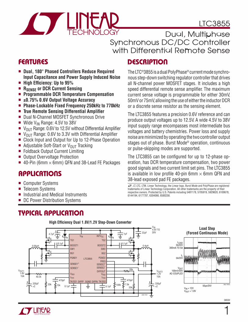
absoluTe MaxiMuM raTings(Note 1)
pin conFiguraTion
Input Supply Voltage (VIN) ......................... –0.3V to 40V Top Side Driver Voltages
BOOST1, BOOST2 .................................. –0.3V to 46VSwitch Voltage (SW1, SW2) ......................... –5V to 40V INTVCC, RUN1, RUN2, PGOOD(s), EXTVCC,
(BOOST1-SW1), (BOOST2-SW2) ............. –0.3V to 6VSENSE1+, SENSE2+, SENSE1–,
SENSE2– Voltages ................................. –0.3V to 13VMODE/PLLIN, ILIM1, ILIM2, TK/SS1, TK/SS2, FREQ,
DIFFOUT, PHASMD Voltages ............. –0.3V to INTVCC
DIFFP, DIFFN .......................................... –0.3V to INTVCC ITEMP1, ITEMP2 Voltages .................... –0.3V to INTVCC ITH1, ITH2, VFB1, VFB2 Voltages .............. –0.3V to INTVCCINTVCC Peak Output Current (Note 8) ..................100mAOperating Junction Temperature Range (Notes 2, 3)
LTC3855 .............................................–40°C to 125°CStorage Temperature Range ...................–65°C to 125°CLead Temperature (Soldering, 10 sec)
(FE Package) ..................................................... 300°C
1
2
3
4
5
6
7
8
9
10
11
12
13
14
15
16
17
18
19
TOP VIEW
FE PACKAGE38-LEAD PLASTIC SSOP
38
37
36
35
34
33
32
31
30
29
28
27
26
25
24
23
22
21
20
ITEMP2
ITEMP1
RUN1
SENSE1+
SENSE1–
TK/SS1
ITH1
VFB1
VFB2
ITH2
TK/SS2
SENSE2+
SENSE2–
DIFFP
DIFFN
DIFFOUT
RUN2
ILIM1
ILIM2
FREQ
MODE/PLLIN
PHASMD
CLKOUT
SW1
TG1
BOOST1
PGND1
BG1
VIN
INTVCC
EXTVCC
BG2
PGND2
BOOST2
TG2
SW2
PGOOD2
PGOOD1
39SGND
TJMAX = 125°C, θJA = 25°C/W
EXPOSED PAD (PIN 39) IS SGND, MUST BE SOLDERED TO PCB
3940 38 37 36 35 34 33 32 31
11 2012 13 14 15
TOP VIEW
41SGND
UJ PACKAGE40-LEAD (6mm 6mm) PLASTIC QFN
16 17 18 19
22
23
24
25
26
27
28
29
9
8
7
6
5
4
3
2
TK/SS1
ITH1
VFB1
SGND
VFB2
ITH2
TK/SS2
SENSE2+
SENSE2–
DIFFP
TG1
BOOST1
PGND1
BG1
VIN
INTVCC
EXTVCC
BG2
PGND2
BOOST2
SENS
E1–
SENS
E1+
RUN1
ITEM
P1
ITEM
P2
FREQ
MOD
E/PL
LIN
PHAS
MD
CLKO
UT
SW1
DIFF
N
DIFF
OUT
RUN2
I LIM
1
I LIM
2
PGOO
D1
PGOO
D2 NC
SW2
TG2
21
30
10
1
TJMAX = 125°C, θJA = 33°C/W
EXPOSED PAD (PIN 41) IS SGND, MUST BE SOLDERED TO PCB
LTC3855
3855f
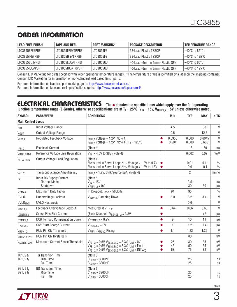
orDer inForMaTionLEAD FREE FINISH TAPE AND REEL PART MARKING* PACKAGE DESCRIPTION TEMPERATURE RANGE
LTC3855EFE#PBF LTC3855EFE#TRPBF LTC3855FE 38-Lead Plastic TSSOP –40°C to 85°C
LTC3855IFE#PBF LTC3855IFE#TRPBF LTC3855FE 38-Lead Plastic TSSOP –40°C to 125°C
LTC3855EUJ#PBF LTC3855EUJ#TRPBF LTC3855UJ 40-Lead (6mm × 6mm) Plastic QFN –40°C to 85°C
LTC3855IUJ#PBF LTC3855IUJ#TRPBF LTC3855UJ 40-Lead (6mm × 6mm) Plastic QFN –40°C to 125°C
Consult LTC Marketing for parts specified with wider operating temperature ranges. *The temperature grade is identified by a label on the shipping container. Consult LTC Marketing for information on non-standard lead based finish parts.For more information on lead free part marking, go to: http://www.linear.com/leadfree/ For more information on tape and reel specifications, go to: http://www.linear.com/tapeandreel/
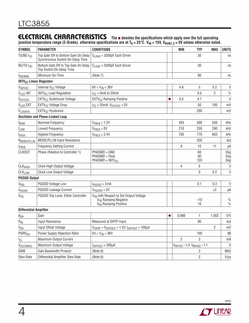
SYMBOL PARAMETER CONDITIONS MIN TYP MAX UNITS
Main Control Loops
VIN Input Voltage Range 4.5 38 V
VOUT Output Voltage Range 0.6 12.5 V
VFB1,2 Regulated Feedback Voltage ITH1,2 Voltage = 1.2V (Note 4) ITH1,2 Voltage = 1.2V (Note 4), TA = 125°C
l
l
0.5955 0.594
0.600 0.600
0.6045 0.606
V V
IFB1,2 Feedback Current (Note 4) –15 –50 nA
VREFLNREG Reference Voltage Line Regulation VIN = 4.5V to 38V (Note 4) 0.002 0.02 %/V
VLOADREG Output Voltage Load Regulation (Note 4) Measured in Servo Loop; ∆ITH Voltage = 1.2V to 0.7V Measured in Servo Loop; ∆ITH Voltage = 1.2V to 1.6V
l
l
0.01
–0.01
0.1
–0.1
% %
gm1,2 Transconductance Amplifier gm ITH1,2 = 1.2V; Sink/Source 5µA; (Note 4) 2 mmho
IQ Input DC Supply Current Normal Mode Shutdown
(Note 5) VIN = 15V VRUN1,2 = 0V
3.5 30
50
mA µA
DFMAX Maximum Duty Factor In Dropout, fOSC = 500kHz 94 95 %
UVLO Undervoltage Lockout VINTVCC Ramping Down l 3.0 3.2 3.4 V
UVLOHYS UVLO Hysteresis 0.6 V
VOVL1,2 Feedback Overvoltage Lockout Measured at VFB1,2 l 0.64 0.66 0.68 V
ISENSE1,2 Sense Pins Bias Current (Each Channel); VSENSE1,2 = 3.3V l ±1 ±2 µA
ITEMP1,2 DCR Tempco Compensation Current VITEMP1,2 = 0.2V l 9 10 11 µA
ITK/SS1,2 Soft-Start Charge Current VTK/SS1,2 = 0V l 1 1.2 1.4 µA
VRUN1,2 RUN Pin ON Threshold VRUN1, VRUN2 Rising l 1.1 1.22 1.35 V
VRUN1,2HYS RUN Pin ON Hysteresis 80 mV
VSENSE(MAX) Maximum Current Sense Threshold VFB1,2 = 0.5V, VSENSE1,2 = 3.3V, ILIM = 0V VFB1,2 = 0.5V, VSENSE1,2 = 3.3V, ILIM = Float VFB1,2 = 0.5V, VSENSE1,2 = 3.3V, ILIM = INTVCC
l
l
l
25 45 68
30 50 75
35 55 82
mV mV mV
TG1, 2 tr TG1, 2 tf
TG Transition Time: Rise Time Fall Time
(Note 6) CLOAD = 3300pF CLOAD = 3300pF
25 25
ns ns
BG1, 2 tr BG1, 2 tf
BG Transition Time: Rise Time Fall Time
(Note 6) CLOAD = 3300pF CLOAD = 3300pF
25 25
ns ns
elecTrical characTerisTics The l denotes the specifications which apply over the full operating junction temperature range (E-Grade), otherwise specifications are at TA = 25°C. VIN = 15V, VRUN1,2 = 5V unless otherwise noted.
LTC3855
3855f
SYMBOL PARAMETER CONDITIONS MIN TYP MAX UNITS
TG/BG t1D Top Gate Off to Bottom Gate On Delay Synchronous Switch-On Delay Time
CLOAD = 3300pF Each Driver 30 ns
BG/TG t2D Bottom Gate Off to Top Gate On Delay Top Switch-On Delay Time
CLOAD = 3300pF Each Driver 30 ns
tON(MIN) Minimum On-Time (Note 7) 90 ns
INTVCC Linear Regulator
VINTVCC Internal VCC Voltage 6V < VIN < 38V 4.8 5 5.2 V
VLDO INT INTVCC Load Regulation ICC = 0mA to 20mA 0.5 2 %
VEXTVCC EXTVCC Switchover Voltage EXTVCC Ramping Positive l 4.5 4.7 V
VLDO EXT EXTVCC Voltage Drop ICC = 20mA, VEXTVCC = 5V 50 100 mV
VLDOHYS EXTVCC Hysteresis 200 mV
Oscillator and Phase-Locked Loop
fNOM Nominal Frequency VFREQ = 1.2V 450 500 550 kHz
fLOW Lowest Frequency VFREQ = 0V 210 250 290 kHz
fHIGH Highest Frequency VFREQ ≥ 2.4V 700 770 850 kHz
RMODE/PLLIN MODE/PLLIN Input Resistance 250 kΩ
IFREQ Frequency Setting Current 9 10 11 µA
CLKOUT Phase (Relative to Controller 1) PHASMD = GND PHASMD = Float PHASMD = INTVCC
60 90
120
Deg Deg Deg
CLKHIGH Clock High Output Voltage 4 5 V
CLKLOW Clock Low Output Voltage 0 0.2 V
PGOOD Output
VPGL PGOOD Voltage Low IPGOOD = 2mA 0.1 0.3 V
IPGOOD PGOOD Leakage Current VPGOOD = 5V ±2 µA
VPG PGOOD Trip Level, Either Controller VFB with Respect to Set Output Voltage VFB Ramping Negative VFB Ramping Positive
–10 10
% %
Differential Amplifier
ADA Gain l 0.998 1 1.002 V/V
RIN Input Resistance Measured at DIFFP Input 80 kΩ
VOS Input Offset Voltage VDIFFP = VDIFFOUT = 1.5V, IDIFFOUT = 100µA 2 mV
PSRROA Power Supply Rejection Ratio 5V < VIN < 38V 100 dB
ICL Maximum Output Current 2 3 mA
VOUT(MAX) Maximum Output Voltage IDIFFOUT = 300µA VINTVCC – 1.4 VINTVCC – 1.1 V
GBW Gain Bandwidth Product (Note 8) 3 MHz
Slew Rate Differential Amplifier Slew Rate (Note 8) 2 V/µs
elecTrical characTerisTics The l denotes the specifications which apply over the full operating junction temperature range (E-Grade), otherwise specifications are at TA = 25°C. VIN = 15V, VRUN1,2 = 5V unless otherwise noted.
LTC3855
3855f
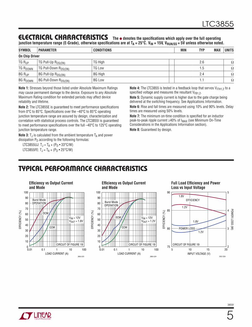
Note 1: Stresses beyond those listed under Absolute Maximum Ratings may cause permanent damage to the device. Exposure to any Absolute Maximum Rating condition for extended periods may affect device reliability and lifetime.Note 2: The LTC3855E is guaranteed to meet performance specifications from 0°C to 85°C. Specifications over the –40°C to 85°C operating junction temperature range are assured by design, characterization and correlation with statistical process controls. The LTC3855I is guaranteed to meet performance specifications over the full –40°C to 125°C operating junction temperature range.Note 3: TJ is calculated from the ambient temperature TA and power dissipation PD according to the following formulas: LTC3855UJ: TJ = TA + (PD • 33°C/W) LTC3855FE: TJ = TA + (PD • 25°C/W)
elecTrical characTerisTics The l denotes the specifications which apply over the full operating junction temperature range (E-Grade), otherwise specifications are at TA = 25°C. VIN = 15V, VRUN/SS = 5V unless otherwise noted.
Note 4: The LTC3855 is tested in a feedback loop that servos VITH1,2 to a specified voltage and measures the resultant VFB1,2.Note 5: Dynamic supply current is higher due to the gate charge being delivered at the switching frequency. See Applications Information.Note 6: Rise and fall times are measured using 10% and 90% levels. Delay times are measured using 50% levels.Note 7: The minimum on-time condition is specified for an inductor peak-to-peak ripple current ≥40% of IMAX (see Minimum On-Time Considerations in the Applications Information section).Note 8: Guaranteed by design.
SYMBOL PARAMETER CONDITIONS MIN TYP MAX UNITS
On Chip Driver
TG RUP TG Pull-Up RDS(ON) TG High 2.6 Ω
TG RDOWN TG Pull-Down RDS(ON) TG Low 1.5 Ω
BG RUP BG Pull-Up RDS(ON) BG High 2.4 Ω
BG RDOWN BG Pull-Down RDS(ON) BG Low 1.1 Ω
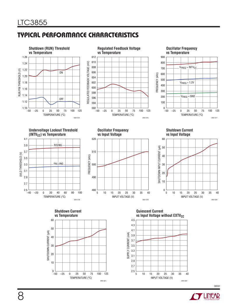
Typical perForMance characTerisTics
Efficiency vs Output Current and Mode
Efficiency vs Output Current and Mode
LOAD CURRENT (A)0.01
EFFI
CIEN
CY (%
)
100
10
90
70
50
30
80
60
40
20
010
3855 G23
10010.1
VIN = 12VVOUT = 1.8V
Burst ModeOPERATION
DCM
CCM
CIRCUIT OF FIGURE 19
LOAD CURRENT (A)0.01
EFFI
CIEN
CY (%
)
100
10
90
70
50
30
80
60
40
20
010
3855 G24
10010.1
VIN = 12VVOUT = 1.2V
Burst ModeOPERATION
DCM
CCM
CIRCUIT OF FIGURE 19
Full Load Efficiency and Power Loss vs Input Voltage
INPUT VOLTAGE (V)5
75
EFFI
CIEN
CY (%
)
80
85
90
2
POWER LOSS (W
)3
4
5
10 2015
3855 G24
1.8V
1.8V
1.2V
1.2V
EFFICIENCY
POWER LOSS
CIRCUIT OF FIGURE 19
LTC3855
3855f
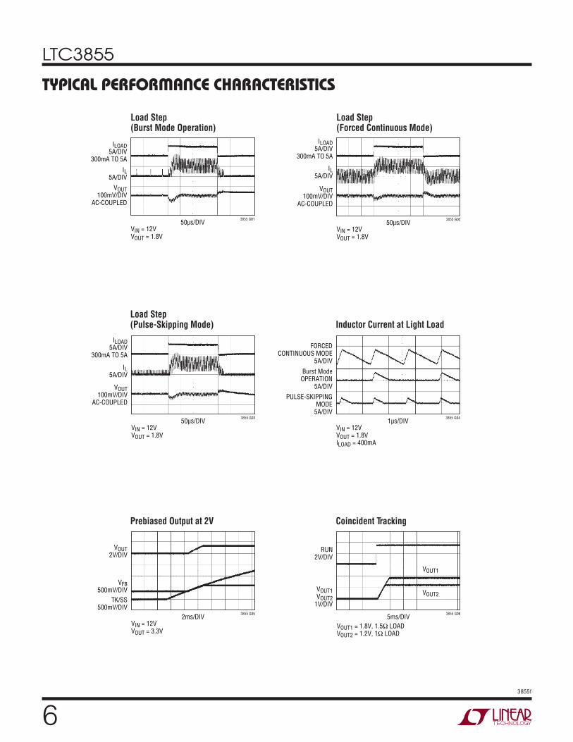
Typical perForMance characTerisTics
Load Step (Burst Mode Operation)
Load Step (Forced Continuous Mode)
Load Step (Pulse-Skipping Mode) Inductor Current at Light Load
Coincident TrackingPrebiased Output at 2V
VIN = 12VVOUT = 1.8V
50µs/DIV3855 G01
IL5A/DIV
VOUT100mV/DIV
AC-COUPLED
ILOAD5A/DIV
300mA TO 5A
VIN = 12VVOUT = 1.8V
50µs/DIV3855 G02
IL5A/DIV
VOUT100mV/DIV
AC-COUPLED
ILOAD5A/DIV
300mA TO 5A
VIN = 12VVOUT = 1.8V
50µs/DIV3855 G03
IL5A/DIV
VOUT100mV/DIV
AC-COUPLED
ILOAD5A/DIV
300mA TO 5A
VIN = 12VVOUT = 1.8VILOAD = 400mA
1µs/DIV3855 G04
FORCEDCONTINUOUS MODE
5A/DIV
Burst ModeOPERATION
5A/DIV
PULSE-SKIPPINGMODE
5A/DIV
VIN = 12VVOUT = 3.3V
2ms/DIV3855 G05
TK/SS500mV/DIV
VFB500mV/DIV
VOUT2V/DIV
5ms/DIV3855 G06
RUN2V/DIV
VOUT1VOUT2
1V/DIV
VOUT1
VOUT2
VOUT1 = 1.8V, 1.5Ω LOADVOUT2 = 1.2V, 1Ω LOAD
LTC3855
3855f
VITH (V)0
–40
V SEN
SE (m
V)
–20
0
20
40
60
80
0.5 1 1.5 2
3855 G10
ILIM = GND
ILIM = FLOAT
ILIM = INTVCC
VSENSE COMMON MODE VOLTAGE (V)0
CURR
ENT
SENS
E TH
RESH
OLD
(mV)
30
40
50
12
20
10
02 6 8 104
60
70
80
3855 G11
ILIM = GND
ILIM = FLOAT
ILIM = INTVCC
60
80
40
20
50
70
30
10
0
DUTY CYCLE (%)0
CURR
ENT
SENS
E TH
RESH
OLD
(mV)
60 10020 40 80
3855 G12
ILIM = GND
ILIM = FLOAT
ILIM = INTVCC
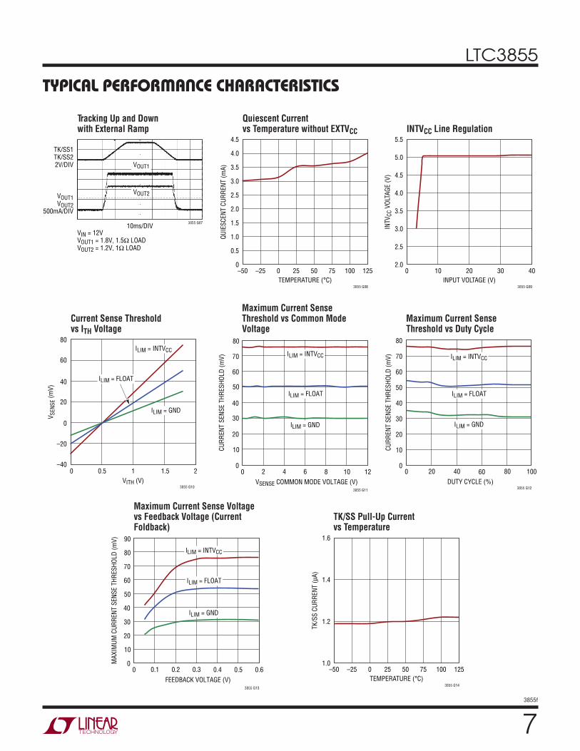
Typical perForMance characTerisTics
Current Sense Threshold vs ITH Voltage
Maximum Current Sense Threshold vs Common Mode Voltage
Maximum Current Sense Threshold vs Duty Cycle
Maximum Current Sense Voltage vs Feedback Voltage (Current Foldback)
TK/SS Pull-Up Current vs Temperature
Tracking Up and Down with External Ramp
Quiescent Currentvs Temperature without EXTVCC INTVCC Line Regulation
VIN = 12VVOUT1 = 1.8V, 1.5Ω LOADVOUT2 = 1.2V, 1Ω LOAD
10ms/DIV3855 G07
TK/SS1TK/SS22V/DIV
VOUT1VOUT2
500mA/DIV
VOUT1
VOUT2
QUIE
SCEN
T CU
RREN
T (m
A)
4.5
4.0
3.0
2.0
1.0
3.5
2.5
1.5
0.5
0
TEMPERATURE (°C)–50 500 100
3855 G08
12525–25 75
INTV
CC V
OLTA
GE (V
)
5.5
5.0
4.5
4.0
3.0
3.5
2.5
2.0
INPUT VOLTAGE (V)0 10 30
3855 G09
4020
FEEDBACK VOLTAGE (V)0
MAX
IMUM
CUR
RENT
SEN
SE T
HRES
HOLD
(mV)
30
40
50
0.6
20
10
00.1 0.3 0.4 0.50.2
60
70
90
80
3855 G13
ILIM = GND
ILIM = FLOAT
ILIM = INTVCC
TK/S
S CU
RREN
T (µ
A)
1.6
1.2
1.4
1.0
TEMPERATURE (°C)–50 500 100
3855 G14
12525–25 75
LTC3855
3855f
Typical perForMance characTerisTics
Undervoltage Lockout Threshold (INTVCC) vs Temperature
Oscillator Frequency vs Input Voltage
Shutdown Current vs Input Voltage
Shutdown Current vs Temperature
Quiescent Current vs Input Voltage without EXTVCC
Shutdown (RUN) Threshold vs Temperature
Regulated Feedback Voltage vs Temperature
Oscillator Frequency vs Temperature
TEMPERATURE (°C)–50
1.26
1.24
1.22
1.20
1.14
1.18
1.16
1.12
1.1025 75
3855 G15
–25 0 50 125100
RUN
PIN
THRE
SHOL
D (V
)
OFF
ON
TEMPERATURE (°C)–50
612
610
608
606
604
602
600
592
594
596
598
25 75
3855 G16
–25 0 50 125100
REGU
LATE
D FE
EDBA
CK V
OLTA
GE (m
V)
TEMPERATURE (°C)–50
900
800
700
500
600
0
100
200
300
400
25 75
3855 G17
–25 0 50 125100
FREQ
UENC
Y (k
Hz)
VFREQ = GND
VFREQ = 1.2V
VFREQ = INTVCC
TEMPERATURE (°C)–40
4.1
3.9
2.9
3.7
2.7
3.1
3.5
2.5
3.3
20 60
3855 G18
–20 0 40 10080
UVLO
THR
ESHO
LD (V
)
FALLING
RISING
INPUT VOLTAGE (V)5
520
510
500
490
48025 35
3855 G19
10 15 20 4030
FREQ
UENC
Y (k
Hz)
INPUT VOLTAGE (V)5
60
50
40
30
20
10
025 35
3855 G20
10 15 20 4030
SHUT
DOW
N IN
PUT
CURR
ENT
(µA)
60
50
40
30
20
10
0
3855 G21
SHUT
DOW
N CU
RREN
T (µ
A)
TEMPERATURE (°C)–50 25 75–25 0 50 125100
INPUT VOLTAGE (V)5
4.5
4.3
4.1
3.3
3.1
2.5
2.7
2.9
3.5
3.7
3.9
25 35
3855 G22
10 15 20 4030
SUPP
LY C
URRE
NT (m
A)
LTC3855
3855f
pin FuncTionsITEMP1, ITEMP2 (Pin 2, Pin 1/Pin 37, Pin 36): Inputs of the temperature sensing comparators. Connect each of these pins to external NTC resistors placed near induc-tors. Floating these pins disables the DCR temperature compensation function.
RUN1, RUN2 (Pin 3, Pin 17/Pin 38, Pin 13): Run Control Inputs. A voltage above 1.2V on either pin turns on the IC. However, forcing either of these pins below 1.2V causes the IC to shut down the circuitry required for that particular channel. There are 1µA pull-up currents for these pins. Once the Run pin rises above 1.2V, an additional 4.5µA pull-up current is added to the pin.
SENSE1+, SENSE2+ (Pin 4, Pin 12/Pin 39, Pin 8): Current Sense Comparator Inputs. The (+) inputs to the current comparators are normally connected to DCR sensing networks or current sensing resistors.
SENSE1–, SENSE2– (Pin 5, Pin 13/Pin 40, Pin 9): Current Sense Comparator Inputs. The (–) inputs to the current comparators are connected to the outputs.
TK/SS1, TK/SS2 (Pin 6, Pin 11/Pin 1, Pin 7): Output Volt-age Tracking and Soft-Start Inputs. When one particular channel is configured to be the master of two channels, a capacitor to ground at this pin sets the ramp rate for the master channel’s output voltage. When the channel is configured to be the slave of two channels, the VFB voltage of the master channel is reproduced by a resistor divider and applied to this pin. Internal soft-start currents of 1.2µA are charging these pins.
ITH1, ITH2 (Pin 7, Pin 10/Pin 2, Pin 6): Current Control Thresholds and Error Amplifier Compensation Points. Each associated channels’ current comparator tripping threshold increases with its ITH control voltage.
VFB1, VFB2 (Pin 8, Pin 9/Pin 3, Pin 5): Error Amplifier Feedback Inputs. These pins receive the remotely sensed feedback voltages for each channel from external resistive dividers across the outputs.
DIFFP (Pin 14/Pin 10): Positive Input of Remote Sens-ing Differential Amplifier. Connect this to the remote load voltage of one of the two channels directly.
DIFFN (Pin 15/Pin 11): Negative Input of Remote Sensing Differential Amplifier. Connect this to the negative terminal of the output capacitors.
DIFFOUT (Pin 16/Pin 12): Output of Remote Sensing Dif-ferential Amplifier. Connect this to VFB1 or VFB2 through a resistive divider.
ILIM1, ILIM2 (Pin 18, Pin 19/Pin 14, Pin 15): Current Comparator Sense Voltage Range Inputs. This pin can be tied to SGND, tied to INTVCC or left floating to set the maximum current sense threshold for each comparator.
PGOOD1, PGOOD2 (Pin 20, Pin 21/Pin 16, Pin 17): Power Good Indicator Output for Each Channel. Open drain logic out that is pulled to ground when either channel output exceeds ±10% regulation window, after the internal 20µs power bad mask timer expires.
EXTVCC (Pin 27/Pin 24): External Power Input to an Inter-nal Switch Connected to INTVCC. This switch closes and supplies the IC power, bypassing the internal low dropout regulator, whenever EXTVCC is higher than 4.7V. Do not exceed 6V on this pin.
INTVCC (Pin 28/Pin 25): Internal 5V Regulator Output. The control circuits are powered from this voltage. Decouple this pin to PGND with a minimum of 4.7µF low ESR tan-talum or ceramic capacitor.
VIN (Pin 29/Pin 26): Main Input Supply. Decouple this pin to PGND with a capacitor (0.1µF to 1µF).
BG1, BG2 (Pin 30, Pin 26/Pin 27, Pin 23): Bottom Gate Driver Outputs. These pins drive the gates of the bottom N-Channel MOSFETs between PGND and INTVCC.
PGND1, PGND2 (Pin 31, Pin 25/Pin 28, Pin 22): Power Ground Pin. Connect this pin closely to the sources of the bottom N-channel MOSFETs, the (–) terminal of CVCC and the (–) terminal of CIN.
(FE38/UJ40)
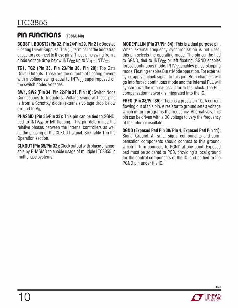
LTC3855
03855f
pin FuncTionsBOOST1, BOOST2 (Pin 32, Pin 24/Pin 29, Pin 21): Boosted Floating Driver Supplies. The (+) terminal of the bootstrap capacitors connect to these pins. These pins swing from a diode voltage drop below INTVCC up to VIN + INTVCC.
TG1, TG2 (Pin 33, Pin 23/Pin 30, Pin 20): Top Gate Driver Outputs. These are the outputs of floating drivers with a voltage swing equal to INTVCC superimposed on the switch nodes voltages.
SW1, SW2 (Pin 34, Pin 22/Pin 31, Pin 19): Switch Node Connections to Inductors. Voltage swing at these pins is from a Schottky diode (external) voltage drop below ground to VIN.
PHASMD (Pin 36/Pin 33): This pin can be tied to SGND, tied to INTVCC or left floating. This pin determines the relative phases between the internal controllers as well as the phasing of the CLKOUT signal. See Table 1 in the Operation section.
CLKOUT (Pin 35/Pin 32): Clock output with phase change-able by PHASMD to enable usage of multiple LTC3855 in multiphase systems.
MODE/PLLIN (Pin 37/Pin 34): This is a dual purpose pin. When external frequency synchronization is not used, this pin selects the operating mode. The pin can be tied to SGND, tied to INTVCC or left floating. SGND enables forced continuous mode. INTVCC enables pulse-skipping mode. Floating enables Burst Mode operation. For external sync, apply a clock signal to this pin. Both channels will go into forced continuous mode and the internal PLL will synchronize the internal oscillator to the clock. The PLL compensation network is integrated into the IC.
FREQ (Pin 38/Pin 35): There is a precision 10µA current flowing out of this pin. A resistor to ground sets a voltage which in turn programs the frequency. Alternatively, this pin can be driven with a DC voltage to vary the frequency of the internal oscillator.
SGND (Exposed Pad Pin 39/ Pin 4, Exposed Pad Pin 41): Signal Ground. All small-signal components and com-pensation components should connect to this ground, which in turn connects to PGND at one point. Exposed pad must be soldered to PCB, providing a local ground for the control components of the IC, and be tied to the PGND pin under the IC.
(FE38/UJ40)
LTC3855
3855f
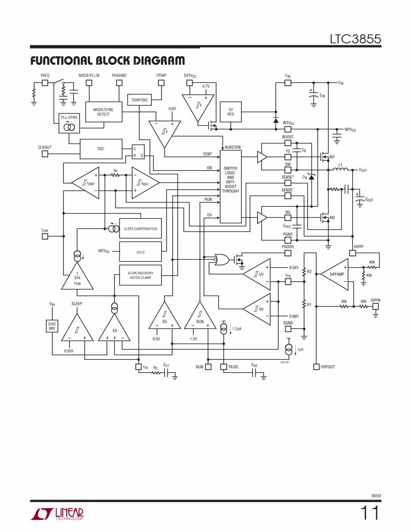
FuncTional block DiagraM
4.7V
–
+
– +
–
+
VIN
1µA
SLOPE COMPENSATION
UVLO
SLOPE RECOVERYACTIVE CLAMP
OSC
TEMPSNS
S
R Q
3k
RUN
SWITCHLOGIC
ANDANTI-
SHOOTTHROUGH
BG
ON
FCNT
0.6V
OV
1.2V0.5V
ITH RC
INTVCC
INTVCC
ILIM
ICMP
CC1
SS SGND
R1
0.66V
R2
RUN
PGND
PGOOD
INTVCC
EXTVCC
IREV
SW
TG CB
VIN
CIN
VIN SLEEP
BOOST
BURSTEN
–
+
–
+
UV
OV
CVCC
VOUT
COUT
M2
M1
L1
DB
MODE/PLLIN
SENSE+
SENSE–
– +0.6VREF
TK/SSRUN
0.55V
– +
VFB
FREQ
PLL-SYNC
MODE/SYNCDETECT
40k
40k
40k
40k
+
5VREG
1.2µA
CSS
+
DIFFP
DIFFN
– +
– +
F
F
CLKOUT
0.54V
–
+
DIFFOUT
PHASMD ITEMP
3855 FBD
151kITHB
–+
EA
+
DIFFAMP
LTC3855
3855f
operaTionMain Control Loop
The LTC3855 is a constant-frequency, current mode step-down controller with two channels operating 180 degrees out-of-phase. During normal operation, each top MOSFET is turned on when the clock for that channel sets the RS latch, and turned off when the main current comparator, ICMP, resets the RS latch. The peak inductor current at which ICMP resets the RS latch is controlled by the voltage on the ITH pin, which is the output of each error ampli-fier EA. The VFB pin receives the voltage feedback signal, which is compared to the internal reference voltage by the EA. When the load current increases, it causes a slight decrease in VFB relative to the 0.6V reference, which in turn causes the ITH voltage to increase until the average inductor current matches the new load current. After the top MOSFET has turned off, the bottom MOSFET is turned on until either the inductor current starts to reverse, as indicated by the reverse current comparator IREV, or the beginning of the next cycle.
INTVCC/EXTVCC Power
Power for the top and bottom MOSFET drivers and most other internal circuitry is derived from the INTVCC pin. When the EXTVCC pin is left open or tied to a voltage less than 4.7V, an internal 5V linear regulator supplies INTVCC power from VIN. If EXTVCC is taken above 4.7V, the 5V regulator is turned off and an internal switch is turned on connecting EXTVCC. Using the EXTVCC pin allows the INTVCC power to be derived from a high efficiency external source such as one of the LTC3855 switching regulator outputs.
Each top MOSFET driver is biased from the floating bootstrap capacitor CB, which normally recharges during each off cycle through an external diode when the top MOSFET turns off. If the input voltage VIN decreases to a voltage close to VOUT, the loop may enter dropout and attempt to turn on the top MOSFET continuously. The dropout detector detects this and forces the top MOSFET off for about one-twelfth of the clock period plus 100ns every third cycle to allow CB to recharge. However, it is recommended that a load be present or the IC operates at low frequency during the drop-out transition to ensure CB is recharged.
Shutdown and Start-Up (RUN1, RUN2 and TK/SS1, TK/SS2 Pins)
The two channels of the LTC3855 can be independently shut down using the RUN1 and RUN2 pins. Pulling either of these pins below 1.2V shuts down the main control loop for that controller. Pulling both pins low disables both controllers and most internal circuits, including the INTVCC regulator. Releasing either RUN pin allows an internal 1µA current to pull up the pin and enable that controller. Alternatively, the RUN pin may be externally pulled up or driven directly by logic. Be careful not to exceed the Absolute Maximum Rating of 6V on this pin.
The start-up of each controller’s output voltage VOUT is controlled by the voltage on the TK/SS1 and TK/SS2 pins. When the voltage on the TK/SS pin is less than the 0.6V internal reference, the LTC3855 regulates the VFB voltage to the TK/SS pin voltage instead of the 0.6V reference. This allows the TK/SS pin to be used to program the soft-start period by connecting an external capacitor from the TK/SS pin to SGND. An internal 1.2µA pull-up current charges this capacitor, creating a voltage ramp on the TK/SS pin. As the TK/SS voltage rises linearly from 0V to 0.6V (and beyond), the output voltage VOUT rises smoothly from zero to its final value. Alternatively the TK/SS pin can be used to cause the start-up of VOUT to “track” that of another supply. Typically, this requires connecting to the TK/SS pin an external resistor divider from the other supply to ground (see the Applications Information section). When the corresponding RUN pin is pulled low to disable a controller, or when INTVCC drops below its undervoltage lockout threshold of 3.2V, the TK/SS pin is pulled low by an internal MOSFET. When in undervoltage lockout, both controllers are disabled and the external MOSFETs are held off.
Light Load Current Operation (Burst Mode Operation, Pulse-Skipping, or Continuous Conduction)
The LTC3855 can be enabled to enter high efficiency Burst Mode operation, constant-frequency pulse-skipping mode, or forced continuous conduction mode. To select forced continuous operation, tie the MODE/PLLIN pin to a DC
LTC3855
3855f
voltage below 0.6V (e.g., SGND). To select pulse-skipping mode of operation, tie the MODE/PLLIN pin to INTVCC. To select Burst Mode operation, float the MODE/PLLIN pin. When a controller is enabled for Burst Mode operation, the peak current in the inductor is set to approximately one-third of the maximum sense voltage even though the voltage on the ITH pin indicates a lower value. If the average inductor current is higher than the load current, the error amplifier EA will decrease the voltage on the ITH pin. When the ITH voltage drops below 0.5V, the internal sleep signal goes high (enabling sleep mode) and both external MOSFETs are turned off.
In sleep mode, the load current is supplied by the output capacitor. As the output voltage decreases, the EA’s output begins to rise. When the output voltage drops enough, the sleep signal goes low, and the controller resumes normal operation by turning on the top external MOSFET on the next cycle of the internal oscillator. When a controller is enabled for Burst Mode operation, the inductor current is not allowed to reverse. The reverse current comparator (IREV) turns off the bottom external MOSFET just before the inductor current reaches zero, preventing it from reversing and going negative. Thus, the controller oper-ates in discontinuous operation. In forced continuous operation, the inductor current is allowed to reverse at light loads or under large transient conditions. The peak inductor current is determined by the voltage on the ITH pin. In this mode, the efficiency at light loads is lower than in Burst Mode operation. However, continuous mode has the advantages of lower output ripple and less interference with audio circuitry.
When the MODE/PLLIN pin is connected to INTVCC, the LTC3855 operates in PWM pulse-skipping mode at light loads. At very light loads, the current comparator ICMP may remain tripped for several cycles and force the external top MOSFET to stay off for the same number of cycles (i.e., skipping pulses). The inductor current is not allowed to reverse (discontinuous operation). This mode, like forced continuous operation, exhibits low output ripple as well as low audio noise and reduced RF interference as compared to Burst Mode operation. It provides higher low current efficiency than forced continuous mode, but not nearly as high as Burst Mode operation.
Multichip Operations (PHASMD and CLKOUT Pins)
The PHASMD pin determines the relative phases between the internal controllers as well as the CLKOUT signal as shown in Table 1. The phases tabulated are relative to zero phase being defined as the rising edge of the clock of phase 1.
Table 1.PHASMD GND FLOAT INTVcc
Phase1 0° 0° 0°
Phase2 180° 180° 240°
CLKOUT 60° 90° 120°
The CLKOUT signal can be used to synchronize additional power stages in a multiphase power supply solution feeding a single, high current output or separate outputs. Input capacitance ESR requirements and efficiency losses are substantially reduced because the peak current drawn from the input capacitor is effectively divided by the number of phases used and power loss is proportional to the RMS current squared. A two stage, single output voltage implementation can reduce input path power loss by 75% and radically reduce the required RMS current rating of the input capacitor(s).
Single Output Multiphase Operation
The LTC3855 can be used for single output multiphase converters by making these connections
• Tie all of the ITH pins together
• Tie all of the VFB pins together
• Tie all of the TK/SS pins together
• Tie all of the RUN pins together
• Tie all of the ITEMP pins together
• Tie all of the ILIM pins together, or tie the ILIM pins to the same potential
For three or more phases, tie the inputs of the unused dif-ferential amplifier(s) to ground. Examples of single output multiphase converters are shown in Figures 20 to 23.
operaTion
LTC3855
3855f
Sensing the Output Voltage with a Differential Amplifier
The LTC3855 includes a low offset, unity gain, high band-width differential amplifier for applications that require true remote sensing. Sensing the load across the load capaci-tors directly greatly benefits regulation in high current, low voltage applications, where board interconnection losses can be a significant portion of the total error budget.
The LTC3855 differential amplifier has a typical output slew rate of 2V/μs. The amplifier is configured for unity gain, meaning that the difference between DIFFP and DIFFN is translated to DIFFOUT, relative to SGND.
Care should be taken to route the DIFFP and DIFFN PCB traces parallel to each other all the way to the terminals of the output capacitor or remote sensing points on the board. In addition, avoid routing these sensitive traces near any high speed switching nodes in the circuit. Ideally, the DIFFP and DIFFN traces should be shielded by a low impedance ground plane to maintain signal integrity.
Inductor DCR Sensing Temperature Compensation and the ITEMP Pins
Inductor DCR current sensing provides a lossless method of sensing the instantaneous current. Therefore, it can provide higher efficiency for applications of high output currents. However the DCR of a copper inductor typically has a positive temperature coefficient. As the temperature of the inductor rises, its DCR value increases. The current limit of the controller is therefore reduced.
LTC3855 offers a method to counter this inaccuracy by allowing the user to place an NTC temperature sensing resistor near the inductor. ITEMP pin, when left floating, is at a voltage around 5V and DCR temperature compensa-tion is disabled. ITEMP pin has a constant 10µA precision current flowing out the pin. By connecting an NTC resistor from ITEMP pin to SGND, the maximum current sense threshold can be varied over temperature according the following equation:
V V
VSENSEMAX ADJ SENSE MAX
ITEMP( ) ( ) •
. –.
=1 8
1 3
Where:
VSENSEMAX(ADJ) is the maximum adjusted current sense threshold.
VSENSE(MAX) is the maximum current sense threshold specified in the electrical characteristics table. It is typi-cally 75mV, 50mV, or 30mV depending on the setting ILIM pins.
VITEMP is the voltage of ITEMP pin.
The valid voltage range for DCR temperature compensa-tion on the ITEMP pin is between 0.5V to 0.2V, with 0.5V or above being no DCR temperature correction and 0.2V the maximum correction. However, if the duty cycle of the controller is less than 25%, the ITEMP range is extended from 0.5V to 0V.
An NTC resistor has a negative temperature coefficient, that means that its value decreases as temperature rises. The VITEMP voltage, therefore, decreases as temperature increases and in turn the VSENSEMAX(ADJ) will increase to compensate the DCR temperature coefficient. The NTC resistor, however, is non-linear and user can linearize its value by building a resistor network with regular resis-tors. Consult the NTC manufacture datasheets for detailed information.
Another use for the ITEMP pins, in addition to NTC com-pensated DCR sensing, is adjusting VSENSE(MAX) to values between the nominal values of 30mV, 50mV and 75mV for a more precise current limit. This is done by applying a voltage less than 0.5V to the ITEMP pin. VSENSE(MAX) will be varied per the above equation and the same duty cycle limitations will apply. The current limit can be adjusted using this method either with a sense resistor or DCR sensing.
For more information see the NTC Compensated DCR Sens-ing paragraph in the Applications Information section.
Frequency Selection and Phase-Locked Loop (FREQ and MODE/PLLIN Pins)
The selection of switching frequency is a trade-off between efficiency and component size. Low frequency opera-tion increases efficiency by reducing MOSFET switching losses, but requires larger inductance and/or capacitance to maintain low output ripple voltage. The switching
operaTion
LTC3855
3855f
frequency of the LTC3855’s controllers can be selected using the FREQ pin. If the MODE/PLLIN pin is not being driven by an external clock source, the FREQ pin can be used to program the controller’s operating frequency from 250kHz to 770kHz.
There is a precision 10µA current flowing out of the FREQ pin, so the user can program the controller’s switching frequency with a single resistor to SGND. A curve is provided later in the application section showing the relationship between the voltage on the FREQ pin and switching frequency.
A phase-locked loop (PLL) is integrated on the LTC3855 to synchronize the internal oscillator to an external clock source that is connected to the MODE/PLLIN pin. The controller is operating in forced continuous mode when it is synchronized.
The PLL loop filter network is integrated inside the LTC3855. The phase-locked loop is capable of locking any frequency within the range of 250kHz to 770kHz. The frequency setting resistor should always be present to set the controller’s initial switching frequency before locking to the external clock.
operaTionPower Good (PGOOD Pins)
When VFB pin voltage is not within ±10% of the 0.6V refer-ence voltage, the PGOOD pin is pulled low. The PGOOD pin is also pulled low when the RUN pin is below 1.2V or when the LTC3855 is in the soft-start or tracking phase. The PGOOD pin will flag power good immediately when the VFB pin is within the ±10% of the reference window. However, there is an internal 20µs power bad mask when VFB goes out the ±10% window. Each channel has its own PGOOD and only responds to its own channel signals. The PGOOD pins are allowed to be pulled up by external resistors to sources of up to 6V.
Output Overvoltage Protection
An overvoltage comparator, OV, guards against transient overshoots (>10%) as well as other more serious condi-tions that may overvoltage the output. In such cases, the top MOSFET is turned off and the bottom MOSFET is turned on until the overvoltage condition is cleared.
applicaTions inForMaTionThe Typical Application on the first page is a basic LTC3855 application circuit. LTC3855 can be configured to use either DCR (inductor resistance) sensing or low value resistor sensing. The choice between the two current sensing schemes is largely a design trade-off between cost, power consumption, and accuracy. DCR sensing is becoming popular because it saves expensive current sensing resis-tors and is more power efficient, especially in high current applications. However, current sensing resistors provide the most accurate current limits for the controller. Other external component selection is driven by the load require-ment, and begins with the selection of RSENSE (if RSENSE is used) and inductor value. Next, the power MOSFETs are se-lected. Finally, input and output capacitors are selected.
Current Limit Programming
The ILIM pin is a tri-level logic input which sets the maxi-mum current limit of the controller. When ILIM is either grounded, floated or tied to INTVCC, the typical value
for the maximum current sense threshold will be 30mV, 50mV or 75mV, respectively. The maximum current sense threshold will be adjusted to values between these settings by applying a voltage less than 0.5V to the ITEMP pin. See the Operation section for more details.
Which setting should be used? For the best current limit accuracy, use the 75mV setting. The 30mV setting will allow for the use of very low DCR inductors or sense resistors, but at the expense of current limit accuracy. The 50mV setting is a good balance between the two. For single output dual phase applications, use the 50mV or 75mV setting for optimal current sharing.
SENSE+ and SENSE– Pins
The SENSE+ and SENSE– pins are the inputs to the current comparators. The common mode input voltage range of the current comparators is 0V to 12.5V. Both SENSE pins are high impedance inputs with small base currents of
LTC3855
3855f
less than 1µA. When the SENSE pins ramp up from 0V to 1.4V, the small base currents flow out of the SENSE pins. When the SENSE pins ramp down from 12.5V to 1.1V, the small base currents flow into the SENSE pins. The high impedance inputs to the current comparators allow accurate DCR sensing. However, care must be taken not to float these pins during normal operation.
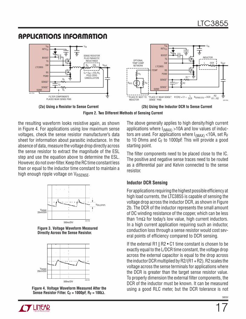
Filter components mutual to the sense lines should be placed close to the LTC3855, and the sense lines should run close together to a Kelvin connection underneath the current sense element (shown in Figure 1). Sensing cur-rent elsewhere can effectively add parasitic inductance and capacitance to the current sense element, degrading the information at the sense terminals and making the programmed current limit unpredictable. If DCR sensing is used (Figure 2b), sense resistor R1 should be placed close to the switching node, to prevent noise from coupling into sensitive small-signal nodes. The capacitor C1 should be placed close to the IC pins.
Because of possible PCB noise in the current sensing loop, the AC current sensing ripple of ∆VSENSE = ∆IL • RSENSE also needs to be checked in the design to get a good signal-to-noise ratio. In general, for a reasonably good PCB layout, a 10mV ∆VSENSE voltage is recommended as a conservative number to start with, either for RSENSE or DCR sensing applications, for duty cycles less than 40%.
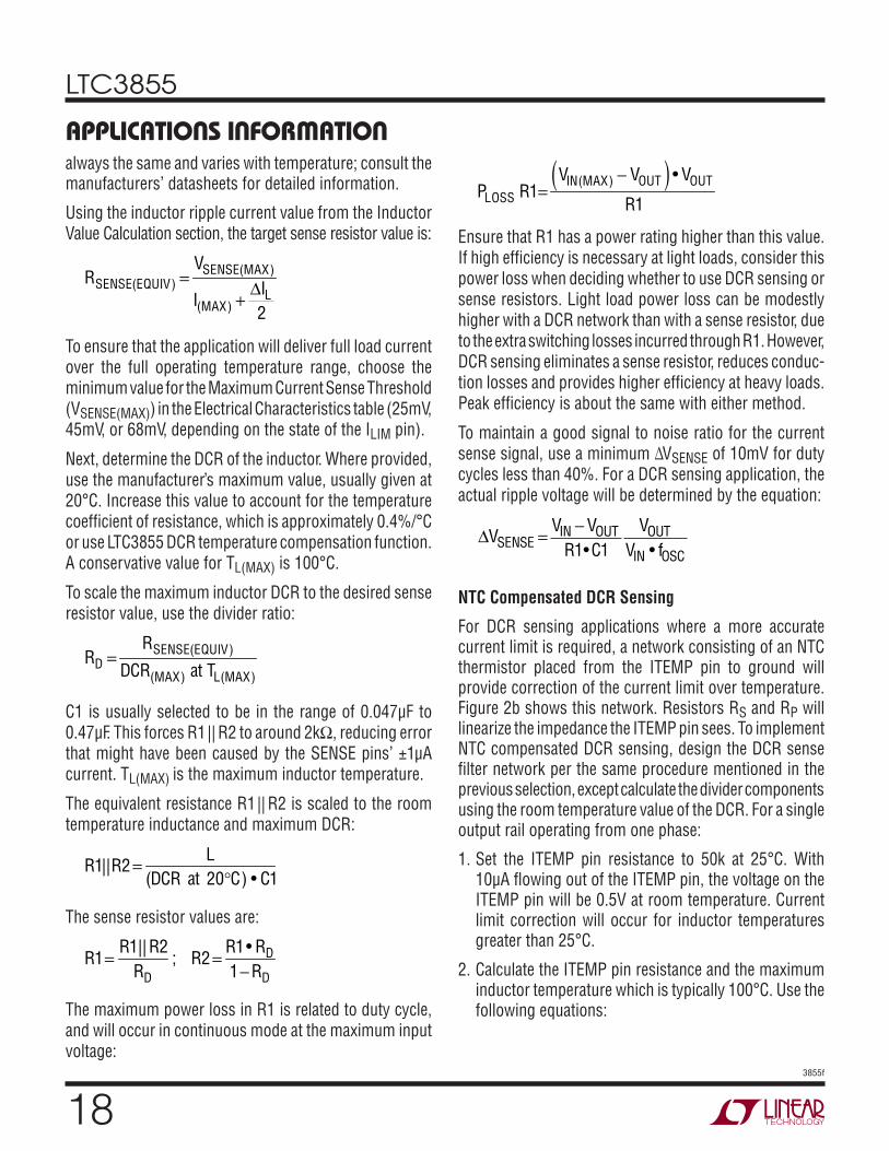
For previous generation current mode controllers, the maximum sense voltage was high enough (e.g., 75mV for the LTC1628 / LTC3728 family) that the voltage drop across the parasitic inductance of the sense resistor represented a relatively small error. For today’s highest current density solutions, however, the value of the sense resistor can be less than 1mΩ and the peak sense voltage can be as low as 20mV. In addition, inductor ripple currents greater than 50% with operation up to 1MHz are becoming more common. Under these conditions the voltage drop across the sense resistor’s parasitic inductance is no longer neg-ligible. A typical sensing circuit using a discrete resistor is shown in Figure 2a. In previous generations of controllers, a small RC filter placed near the IC was commonly used to reduce the effects of capacitive and inductive noise coupled inthe sense traces on the PCB. A typical filter consists of two series 10Ω resistors connected to a parallel 1000pF capacitor, resulting in a time constant of 20ns.
This same RC filter, with minor modifications, can be used to extract the resistive component of the current sense signal in the presence of parasitic inductance. For example, Figure 3 illustrates the voltage waveform across a 2mΩ sense resistor with a 2010 footprint for the 1.2V/15A converter operating at 100% load. The waveform is the superposition of a purely resistive component and a purely inductive component. It was measured using two scope probes and waveform math to obtain a differential measurement. Based on additional measurements of the inductor ripple current and the on-time and off-time of the top switch, the value of the parasitic inductance was determined to be 0.5nH using the equation:
ESL
V
It tt t
ESL STEP
L
ON OFF
ON OFF=
∆ +( ) •
If the RC time constant is chosen to be close to the parasitic inductance divided by the sense resistor (L/R),
applicaTions inForMaTion
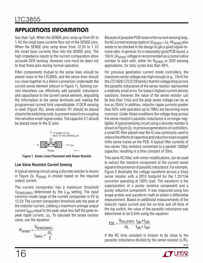
Figure 1. Sense Lines Placement with Sense Resistor
COUT
TO SENSE FILTER,NEXT TO THE CONTROLLER
RSENSE 3855 F01
Low Value Resistors Current Sensing
A typical sensing circuit using a discrete resistor is shown in Figure 2a. RSENSE is chosen based on the required output current.
The current comparator has a maximum threshold VSENSE(MAX) determined by the ILIM setting. The input common mode range of the current comparator is 0V to 12.5V. The current comparator threshold sets the peak of the inductor current, yielding a maximum average output current IMAX equal to the peak value less half the peak-to-peak ripple current, ∆IL. To calculate the sense resistor value, use the equation:
RSENSE =VSENSE(MAX)
I(MAX) +∆IL2
LTC3855
3855f
The above generally applies to high density/high current applications where I(MAX) >10A and low values of induc-tors are used. For applications where I(MAX) <10A, set RF to 10 Ohms and CF to 1000pF. This will provide a good starting point.
The filter components need to be placed close to the IC. The positive and negative sense traces need to be routed as a differential pair and Kelvin connected to the sense resistor.
Inductor DCR Sensing
For applications requiring the highest possible efficiency at high load currents, the LTC3855 is capable of sensing the voltage drop across the inductor DCR, as shown in Figure 2b. The DCR of the inductor represents the small amount of DC winding resistance of the copper, which can be less than 1mΩ for today’s low value, high current inductors. In a high current application requiring such an inductor, conduction loss through a sense resistor would cost sev-eral points of efficiency compared to DCR sensing.
If the external R1|| R2 • C1 time constant is chosen to be exactly equal to the L/DCR time constant, the voltage drop across the external capacitor is equal to the drop across the inductor DCR multiplied by R2/(R1 + R2). R2 scales the voltage across the sense terminals for applications where the DCR is greater than the target sense resistor value. To properly dimension the external filter components, the DCR of the inductor must be known. It can be measured using a good RLC meter, but the DCR tolerance is not
applicaTions inForMaTion
Figure 2. Two Different Methods of Sensing Current
(2a) Using a Resistor to Sense Current (2b) Using the Inductor DCR to Sense Current
VIN VININTVCC
BOOSTTG
SW
BG
PGND
FILTER COMPONENTSPLACED NEAR SENSE PINS
SENSE+
SENSE–
SGND
LTC3855VOUT
3855 F02a
CF • 2RF ≤ ESL/RSPOLE-ZERO
CANCELLATION
SENSE RESISTORPLUS PARASITIC
INDUCTANCE
RS ESL
CF
RF
RF
VIN VININTVCC
ITEMP
BOOST
TG
SW
BG
PGND
*PLACE C1 NEAR SENSE+, SENSE– PINS
**PLACE R1 NEXT TO INDUCTOR
INDUCTOR
DCRL
SENSE+
SENSE–SGND
LTC3855
OPTIONALTEMP COMPNETWORK
VOUT
3855 F02b
R1**
R2C1*RPRNTC
RS
R1||R2 × C1 = L
DCRRSENSE(EQ) = DCR R2
R1 + R2
Figure 3. Voltage Waveform Measured Directly Across the Sense Resistor.
Figure 4. Voltage Waveform Measured After the Sense Resistor Filter. CF = 1000pF, RF = 100Ω.
500ns/DIV
VSENSE20mV/DIV
3855 F03
VESL(STEP)
500ns/DIV
VSENSE20mV/DIV
3855 F04
the resulting waveform looks resistive again, as shown in Figure 4. For applications using low maximum sense voltages, check the sense resistor manufacturer’s data sheet for information about parasitic inductance. In the absence of data, measure the voltage drop directly across the sense resistor to extract the magnitude of the ESL step and use the equation above to determine the ESL. However, do not over-filter. Keep the RC time constant less than or equal to the inductor time constant to maintain a high enough ripple voltage on VRSENSE.
LTC3855
3855f
applicaTions inForMaTionalways the same and varies with temperature; consult the manufacturers’ datasheets for detailed information.
Using the inductor ripple current value from the Inductor Value Calculation section, the target sense resistor value is:
RSENSE(EQUIV) =VSENSE(MAX)
I(MAX) +∆IL2
To ensure that the application will deliver full load current over the full operating temperature range, choose the minimum value for the Maximum Current Sense Threshold (VSENSE(MAX)) in the Electrical Characteristics table (25mV, 45mV, or 68mV, depending on the state of the ILIM pin).
Next, determine the DCR of the inductor. Where provided, use the manufacturer’s maximum value, usually given at 20°C. Increase this value to account for the temperature coefficient of resistance, which is approximately 0.4%/°C or use LTC3855 DCR temperature compensation function. A conservative value for TL(MAX) is 100°C.
To scale the maximum inductor DCR to the desired sense resistor value, use the divider ratio:
RD =
RSENSE(EQUIV)
DCR(MAX) at TL(MAX)
C1 is usually selected to be in the range of 0.047µF to 0.47µF. This forces R1|| R2 to around 2kΩ, reducing error that might have been caused by the SENSE pins’ ±1µA current. TL(MAX) is the maximum inductor temperature.
The equivalent resistance R1|| R2 is scaled to the room temperature inductance and maximum DCR:
R1||R2= L
(DCR at 20°C) • C1
The sense resistor values are:
R1=
R1||R2RD
; R2=R1• RD1−RD
The maximum power loss in R1 is related to duty cycle, and will occur in continuous mode at the maximum input voltage:
PLOSS R1=
VIN(MAX) − VOUT( ) • VOUT
R1
Ensure that R1 has a power rating higher than this value. If high efficiency is necessary at light loads, consider this power loss when deciding whether to use DCR sensing or sense resistors. Light load power loss can be modestly higher with a DCR network than with a sense resistor, due to the extra switching losses incurred through R1. However, DCR sensing eliminates a sense resistor, reduces conduc-tion losses and provides higher efficiency at heavy loads. Peak efficiency is about the same with either method.
To maintain a good signal to noise ratio for the current sense signal, use a minimum ∆VSENSE of 10mV for duty cycles less than 40%. For a DCR sensing application, the actual ripple voltage will be determined by the equation:
∆ = −
VV V
R CV
V fSENSEIN OUT OUT
IN OSC1 1• •
NTC Compensated DCR Sensing
For DCR sensing applications where a more accurate current limit is required, a network consisting of an NTC thermistor placed from the ITEMP pin to ground will provide correction of the current limit over temperature. Figure 2b shows this network. Resistors RS and RP will linearize the impedance the ITEMP pin sees. To implement NTC compensated DCR sensing, design the DCR sense filter network per the same procedure mentioned in the previous selection, except calculate the divider components using the room temperature value of the DCR. For a single output rail operating from one phase:
1. Set the ITEMP pin resistance to 50k at 25°C. With 10µA flowing out of the ITEMP pin, the voltage on the ITEMP pin will be 0.5V at room temperature. Current limit correction will occur for inductor temperatures greater than 25°C.
2. Calculate the ITEMP pin resistance and the maximum inductor temperature which is typically 100°C. Use the following equations:
LTC3855
3855f
R
VµAITEMP C
ITEMP C100
10010
=
V VI DCR MAX R
R R
ITEMP C
MAX
100 0 5 1 32
1 2
= − •• •
+•
. .( ) (1100 25 0 4
100° − ° •C C
VSENSE MAX
) .
( )
Calculate the values for RP and RS. A simple method is to graph the following RS versus RP equations with RS on the y-axis and RP on the x-axis.
RS = RITEMP25C – RNTC25C|| RP
RS = RITEMP100C – RNTC100C|| RP
Next, find the value of RP that satisfies both equations which will be the point where the curves intersect. Once RP is known, solve for RS.
The resistance of the NTC thermistor can be obtained from the vendor’s data sheet either in the form of graphs, tabulated data, or formulas. The approximate value for the NTC thermistor for a given temperature can be calculated from the following equation:
R R B
T TOO
= • • + − +
exp 1273
1273
where
R = Resistance at temperature T, which is in degrees C
RO = Resistance at temperature TO, typically 25°C
B = B-constant of the thermistor
Figure 5 shows a typical resistance curve for a 100k therm-istor and the ITEMP pin network over temperature.
Starting values for the NTC compensation network are:
• NTC RO = 100k
• RS = 20k
• RP = 50k
But, the final values should be calculated using the above equations and checked at 25°C and 100°C.
After determining the components for the temperature compensation network, check the results by plotting IMAX versus inductor temperature using the following equations:
IV V
DCR MAX
MAX
SENSEMAX ADJ SENSE
=−
°
( )
( )
∆2
at 25 CC T CL MAX• + − °( )•
1 250 4100( )
.
where
V V
V VASENSEMAX ADJ SENSE MAX
ITEMP( ) ( )
..
= •−
−1 8
1 3
VITEMP = 10µA • (RS + RP|| RNTC)
Use typical values for VSENSE(MAX). Subtracting constant A will provide a minimum value for VSENSE(MAX). These values are summarized in Table 2.
Table 2.ILIM GND FLOAT INTVCC
VSENSE(MAX) TYP 30mV 50mV 75mV
A 5mV 5mV 7mV
The resulting current limit should be greater than or equal to IMAX for inductor temperatures between 25°C and 100°C.
Typical values for the NTC compensation network are:
• NTC RO = 100k, B-constant = 3000 to 4000
• RS ≈ 20k
• RP ≈ 50k
Generating the IMAX versus inductor temperature curve plot first using the above values as a starting point and then adjusting the RS and RP values as necessary is another approach. Figure 6 shows a typical curve of IMAX versus inductor temperature. For PolyPhase applications, tie the ITEMP pins together and calculate for an ITEMP pin cur-rent of 10µA • #phases.
The same thermistor network can be used to correct for temperatures less than 25°C. But make sure VITEMP is
applicaTions inForMaTion
LTC3855
03855f
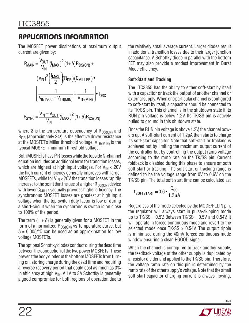
greater than 0.2V for duty cycles of 25% or more, oth-erwise temperature correction may not occur at elevated ambients. For the most accurate temperature detection, place the thermistors next to the inductors as shown in Figure 7. Take care to keep the ITEMP pins away from the switch nodes.
Slope Compensation and Inductor Peak Current
Slope compensation provides stability in constant- frequency architectures by preventing subharmonic oscil-lations at high duty cycles. It is accomplished internally by adding a compensating ramp to the inductor current signal at duty cycles in excess of 40%. Normally, this results in a reduction of maximum inductor peak current for duty cycles >40%. However, the LTC3855 uses a scheme that counteracts this compensating ramp, which allows the
maximum inductor peak current to remain unaffected throughout all duty cycles.
Inductor Value Calculation
Given the desired input and output voltages, the inductor value and operating frequency fOSC directly determine the inductor’s peak-to-peak ripple current:
IRIPPLE =
VOUTVIN
VIN – VOUTfOSC •L
Lower ripple current reduces core losses in the inductor, ESR losses in the output capacitors, and output voltage ripple. Thus, highest efficiency operation is obtained at low frequency with a small ripple current. Achieving this, however, requires a large inductor.
Figure 7. Thermistor Locations. Place Thermistor Next to Inductor(s) for Accurate Sensing of the Inductor Temperature, but Keep the ITEMP Pins Away from the Switch Nodes and Gate Drive Traces
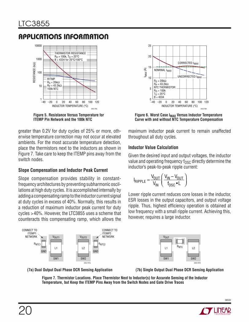
Figure 5. Resistance Versus Temperature for ITEMP Pin Network and the 100k NTC
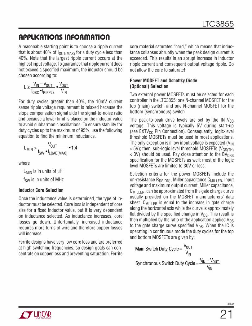
Figure 6. Worst Case IMAX Versus Inductor Temperature Curve with and without NTC Temperature Compensation
applicaTions inForMaTion
(7a) Dual Output Dual Phase DCR Sensing Application (7b) Single Output Dual Phase DCR Sensing Application
10000
1000
100
10
1
INDUCTOR TEMPERATURE (°C)–40
RESI
STAN
CE (k
Ω)
0 40–20 20 80
3855 F05
12060 100
RITMPRS = 20kΩRP = 43.2kΩ100k NTC
THERMISTOR RESISTANCERO = 100k, TO = 25°CB = 4334 for 25°C/100°C
25
20
15
10
5
0
INDUCTOR TEMPERATURE (°C)–40
I MAX
(A)
0 40–20 20 80
3855 F06
12060 100
RS = 20kΩRP = 43.2kΩNTC THERMISTOR:RO = 100kTO = 25°CB = 4334
CORRECTED IMAX
UNCORRECTED IMAX
NOMINAL IMAX
CONNECT TOITEMP1
NETWORK
CONNECT TOITEMP2NETWORK
RNTC2
GND
RNTC1
GND
3855 F07a
VOUT1
SW1
L1
VOUT2
SW2
L2 RNTC
3855 F07b
VOUT
SW1
L1
SW2
L2
LTC3855
3855f
applicaTions inForMaTionA reasonable starting point is to choose a ripple current that is about 40% of IOUT(MAX) for a duty cycle less than 40%. Note that the largest ripple current occurs at the highest input voltage. To guarantee that ripple current does not exceed a specified maximum, the inductor should be chosen according to:
L ≥
VIN – VOUTfOSC •IRIPPLE
•VOUTVIN
For duty cycles greater than 40%, the 10mV current sense ripple voltage requirement is relaxed because the slope compensation signal aids the signal-to-noise ratio and because a lower limit is placed on the inductor value to avoid subharmonic oscillations. To ensure stability for duty cycles up to the maximum of 95%, use the following equation to find the minimum inductance.
L
Vf IMIN
OUT
SW LOAD MAX>
•• .
( )1 4
where
LMIN is in units of µH
fSW is in units of MHz
Inductor Core Selection
Once the inductance value is determined, the type of in-ductor must be selected. Core loss is independent of core size for a fixed inductor value, but it is very dependent on inductance selected. As inductance increases, core losses go down. Unfortunately, increased inductance requires more turns of wire and therefore copper losses will increase.
Ferrite designs have very low core loss and are preferred at high switching frequencies, so design goals can con-centrate on copper loss and preventing saturation. Ferrite
core material saturates “hard,” which means that induc-tance collapses abruptly when the peak design current is exceeded. This results in an abrupt increase in inductor ripple current and consequent output voltage ripple. Do not allow the core to saturate!
Power MOSFET and Schottky Diode (Optional) Selection
Two external power MOSFETs must be selected for each controller in the LTC3855: one N-channel MOSFET for the top (main) switch, and one N-channel MOSFET for the bottom (synchronous) switch.
The peak-to-peak drive levels are set by the INTVCC voltage. This voltage is typically 5V during start-up (see EXTVCC Pin Connection). Consequently, logic-level threshold MOSFETs must be used in most applications. The only exception is if low input voltage is expected (VIN < 5V); then, sub-logic level threshold MOSFETs (VGS(TH) < 3V) should be used. Pay close attention to the BVDSS specification for the MOSFETs as well; most of the logic level MOSFETs are limited to 30V or less.
Selection criteria for the power MOSFETs include the on-resistance RDS(ON), Miller capacitance CMILLER, input voltage and maximum output current. Miller capacitance, CMILLER, can be approximated from the gate charge curve usually provided on the MOSFET manufacturers’ data sheet. CMILLER is equal to the increase in gate charge along the horizontal axis while the curve is approximately flat divided by the specified change in VDS. This result is then multiplied by the ratio of the application applied VDS to the gate charge curve specified VDS. When the IC is operating in continuous mode the duty cycles for the top and bottom MOSFETs are given by:
Main Switch Duty Cycle =VOUTVIN
Synchronous Switch Duty Cycle =VIN – VOUT
VIN
LTC3855
3855f
applicaTions inForMaTionThe MOSFET power dissipations at maximum output current are given by:
PVV
I R
V I
MAINOUT
INMAX DS ON
INMAX
= ( ) +( ) +
( )
2
2
1 d ( )
22
1 1
( )( )
+
R C
V V V
DR MILLER
INTVCC TH MIN
•
– ( ) TTH MINOSC
SYNCIN OUT
INMAX
f
PV V
VI
( )•
–
= ( )) +( )2 1 d RDS ON( )
where d is the temperature dependency of RDS(ON) and RDR (approximately 2Ω) is the effective driver resistance at the MOSFET’s Miller threshold voltage. VTH(MIN) is the typical MOSFET minimum threshold voltage.
Both MOSFETs have I2R losses while the topside N-channel equation includes an additional term for transition losses, which are highest at high input voltages. For VIN < 20V the high current efficiency generally improves with larger MOSFETs, while for VIN > 20V the transition losses rapidly increase to the point that the use of a higher RDS(ON) device with lower CMILLER actually provides higher efficiency. The synchronous MOSFET losses are greatest at high input voltage when the top switch duty factor is low or during a short-circuit when the synchronous switch is on close to 100% of the period.
The term (1 + d) is generally given for a MOSFET in the form of a normalized RDS(ON) vs Temperature curve, but d = 0.005/°C can be used as an approximation for low voltage MOSFETs.
The optional Schottky diodes conduct during the dead time between the conduction of the two power MOSFETs. These prevent the body diodes of the bottom MOSFETs from turn-ing on, storing charge during the dead time and requiring a reverse recovery period that could cost as much as 3% in efficiency at high VIN. A 1A to 3A Schottky is generally a good compromise for both regions of operation due to
the relatively small average current. Larger diodes result in additional transition losses due to their larger junction capacitance. A Schottky diode in parallel with the bottom FET may also provide a modest improvement in Burst Mode efficiency.
Soft-Start and Tracking
The LTC3855 has the ability to either soft-start by itself with a capacitor or track the output of another channel or external supply. When one particular channel is configured to soft-start by itself, a capacitor should be connected to its TK/SS pin. This channel is in the shutdown state if its RUN pin voltage is below 1.2V. Its TK/SS pin is actively pulled to ground in this shutdown state.
Once the RUN pin voltage is above 1.2V, the channel pow-ers up. A soft-start current of 1.2µA then starts to charge its soft-start capacitor. Note that soft-start or tracking is achieved not by limiting the maximum output current of the controller but by controlling the output ramp voltage according to the ramp rate on the TK/SS pin. Current foldback is disabled during this phase to ensure smooth soft-start or tracking. The soft-start or tracking range is defined to be the voltage range from 0V to 0.6V on the TK/SS pin. The total soft-start time can be calculated as:
tSOFTSTART = 0.6 •
CSS1.2µA
Regardless of the mode selected by the MODE/PLLIN pin, the regulator will always start in pulse-skipping mode up to TK/SS = 0.5V. Between TK/SS = 0.5V and 0.54V, it will operate in forced continuous mode and revert to the selected mode once TK/SS > 0.54V. The output ripple is minimized during the 40mV forced continuous mode window ensuring a clean PGOOD signal.
When the channel is configured to track another supply, the feedback voltage of the other supply is duplicated by a resistor divider and applied to the TK/SS pin. Therefore, the voltage ramp rate on this pin is determined by the ramp rate of the other supply’s voltage. Note that the small soft-start capacitor charging current is always flowing,
LTC3855
3855f
applicaTions inForMaTionproducing a small offset error. To minimize this error, select the tracking resistive divider value to be small enough to make this error negligible.
In order to track down another channel or supply after the soft-start phase expires, the LTC3855 is forced into continuous mode of operation as soon as VFB is below the undervoltage threshold of 0.54V regardless of the setting on the MODE/PLLIN pin. However, the LTC3855 should always be set in force continuous mode tracking down when there is no load. After TK/SS drops below 0.1V, its channel will operate in discontinuous mode.
Output Voltage Tracking
The LTC3855 allows the user to program how its output ramps up and down by means of the TK/SS pins. Through these pins, the output can be set up to either coincidentally or ratiometrically track another supply’s output, as shown in Figure 8. In the following discussions, VOUT1 refers to the LTC3855’s output 1 as a master channel and VOUT2 refers to the LTC3855’s output 2 as a slave channel. In practice, though, either phase can be used as the master.
To implement the coincident tracking in Figure 8a, con-nect an additional resistive divider to VOUT1 and connect its midpoint to the TK/SS pin of the slave channel. The ratio of this divider should be the same as that of the slave channel’s feedback divider shown in Figure 9a. In this tracking mode, VOUT1 must be set higher than VOUT2. To implement the ratiometric tracking in Figure 9b, the ratio of the VOUT2 divider should be exactly the same as the master channel’s feedback divider shown in Figure 9b. By select-ing different resistors, the LTC3855 can achieve different modes of tracking including the two in Figure 8.
So which mode should be programmed? While either mode in Figure 8 satisfies most practical applications, some tradeoffs exist. The ratiometric mode saves a pair of resistors, but the coincident mode offers better output regulation.
When the master channel’s output experiences dynamic excursion (under load transient, for example), the slave channel output will be affected as well. For better output regulation, use the coincident tracking mode instead of ratiometric.
Figure 8. Two Different Modes of Output Voltage Tracking
Figure 9. Setup for Coincident and Ratiometric Tracking
TIME
(8a) Coincident Tracking
VOUT1
VOUT2
OUTP
UT V
OLTA
GE
3855 F08a
VOUT1
VOUT2
TIME 3855 F08b
(8b) Ratiometric Tracking
OUTP
UT V
OLTA
GE
R3 R1
R4 R2
R3VOUT2
R4
(9a) Coincident Tracking Setup
TOVFB1PIN
TOTK/SS2
PIN
TOVFB2PIN
VOUT1R1
R2
R3VOUT2
R4
3855 F09
(9b) Ratiometric Tracking Setup
TOVFB1PIN
TOTK/SS2
PIN
TOVFB2PIN
VOUT1
LTC3855
3855f
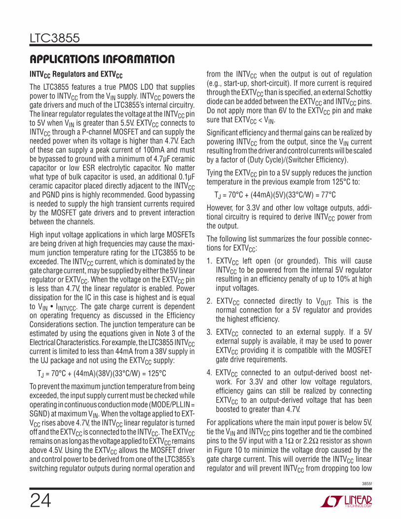
applicaTions inForMaTionINTVCC Regulators and EXTVCC
The LTC3855 features a true PMOS LDO that supplies power to INTVCC from the VIN supply. INTVCC powers the gate drivers and much of the LTC3855’s internal circuitry. The linear regulator regulates the voltage at the INTVCC pin to 5V when VIN is greater than 5.5V. EXTVCC connects to INTVCC through a P-channel MOSFET and can supply the needed power when its voltage is higher than 4.7V. Each of these can supply a peak current of 100mA and must be bypassed to ground with a minimum of 4.7µF ceramic capacitor or low ESR electrolytic capacitor. No matter what type of bulk capacitor is used, an additional 0.1µF ceramic capacitor placed directly adjacent to the INTVCC and PGND pins is highly recommended. Good bypassing is needed to supply the high transient currents required by the MOSFET gate drivers and to prevent interaction between the channels.
High input voltage applications in which large MOSFETs are being driven at high frequencies may cause the maxi-mum junction temperature rating for the LTC3855 to be exceeded. The INTVCC current, which is dominated by the gate charge current, may be supplied by either the 5V linear regulator or EXTVCC. When the voltage on the EXTVCC pin is less than 4.7V, the linear regulator is enabled. Power dissipation for the IC in this case is highest and is equal to VIN • IINTVCC. The gate charge current is dependent on operating frequency as discussed in the Efficiency Considerations section. The junction temperature can be estimated by using the equations given in Note 3 of the Electrical Characteristics. For example, the LTC3855 INTVCC current is limited to less than 44mA from a 38V supply in the UJ package and not using the EXTVCC supply:
TJ = 70°C + (44mA)(38V)(33°C/W) = 125°C
To prevent the maximum junction temperature from being exceeded, the input supply current must be checked while operating in continuous conduction mode (MODE/PLLIN = SGND) at maximum VIN. When the voltage applied to EXT-VCC rises above 4.7V, the INTVCC linear regulator is turned off and the EXTVCC is connected to the INTVCC. The EXTVCC remains on as long as the voltage applied to EXTVCC remains above 4.5V. Using the EXTVCC allows the MOSFET driver and control power to be derived from one of the LTC3855’s switching regulator outputs during normal operation and
from the INTVCC when the output is out of regulation (e.g., start-up, short-circuit). If more current is required through the EXTVCC than is specified, an external Schottky diode can be added between the EXTVCC and INTVCC pins. Do not apply more than 6V to the EXTVCC pin and make sure that EXTVCC < VIN.
Significant efficiency and thermal gains can be realized by powering INTVCC from the output, since the VIN current resulting from the driver and control currents will be scaled by a factor of (Duty Cycle)/(Switcher Efficiency).
Tying the EXTVCC pin to a 5V supply reduces the junction temperature in the previous example from 125°C to:
TJ = 70°C + (44mA)(5V)(33°C/W) = 77°C
However, for 3.3V and other low voltage outputs, addi-tional circuitry is required to derive INTVCC power from the output.
The following list summarizes the four possible connec-tions for EXTVCC:
1. EXTVCC left open (or grounded). This will cause INTVCC to be powered from the internal 5V regulator resulting in an efficiency penalty of up to 10% at high input voltages.
2. EXTVCC connected directly to VOUT. This is the normal connection for a 5V regulator and provides the highest efficiency.
3. EXTVCC connected to an external supply. If a 5V external supply is available, it may be used to power EXTVCC providing it is compatible with the MOSFET gate drive requirements.
4. EXTVCC connected to an output-derived boost net- work. For 3.3V and other low voltage regulators, efficiency gains can still be realized by connecting EXTVCC to an output-derived voltage that has been boosted to greater than 4.7V.
For applications where the main input power is below 5V, tie the VIN and INTVCC pins together and tie the combined pins to the 5V input with a 1Ω or 2.2Ω resistor as shown in Figure 10 to minimize the voltage drop caused by the gate charge current. This will override the INTVCC linear regulator and will prevent INTVCC from dropping too low
LTC3855
3855f
applicaTions inForMaTiondue to the dropout voltage. Make sure the INTVCC voltage is at or exceeds the RDS(ON) test voltage for the MOSFET which is typically 4.5V for logic level devices.
Another way to detect an undervoltage condition is to monitor the VIN supply. Because the RUN pins have a precision turn-on reference of 1.2V, one can use a resistor divider to VIN to turn on the IC when VIN is high enough. An extra 4.5µA of current flows out of the RUN pin once the RUN pin voltage passes 1.2V. One can program the hysteresis of the run comparator by adjusting the values of the resistive divider. For accurate VIN undervoltage detection, VIN needs to be higher than 4.5V.
CIN and COUT Selection
The selection of CIN is simplified by the 2-phase architec-ture and its impact on the worst-case RMS current drawn through the input network (battery/fuse/capacitor). It can be shown that the worst-case capacitor RMS current occurs when only one controller is operating. The controller with the highest (VOUT)(IOUT) product needs to be used in the formula below to determine the maximum RMS capacitor current requirement. Increasing the output current drawn from the other controller will actually decrease the input RMS ripple current from its maximum value. The out-of-phase technique typically reduces the input capacitor’s RMS ripple current by a factor of 30% to 70% when compared to a single phase power supply solution.
In continuous mode, the source current of the top MOSFET is a square wave of duty cycle (VOUT)/(VIN). To prevent large voltage transients, a low ESR capacitor sized for the maximum RMS current of one channel must be used. The maximum RMS capacitor current is given by:
CIN Required IRMS ≈
IMAXVIN
VOUT( ) VIN – VOUT( ) 1/2
This formula has a maximum at VIN = 2VOUT, where IRMS = IOUT/2. This simple worst-case condition is commonly used for design because even significant deviations do not of-fer much relief. Note that capacitor manufacturers’ ripple current ratings are often based on only 2000 hours of life. This makes it advisable to further derate the capacitor, or to choose a capacitor rated at a higher temperature than required. Several capacitors may be paralleled to meet size or height requirements in the design. Due to the high operating frequency of the LTC3855, ceramic capacitors
Figure 10. Setup for a 5V Input
INTVCC
LTC3855 RVIN
1Ω
CIN
3855 F07
4.7µF
5V
CINTVCC +
VIN
Topside MOSFET Driver Supply (CB, DB)
External bootstrap capacitors CB connected to the BOOST pins supply the gate drive voltages for the topside MOSFETs. Capacitor CB in the Functional Diagram is charged though external diode DB from INTVCC when the SW pin is low. When one of the topside MOSFETs is to be turned on, the driver places the CB voltage across the gate source of the desired MOSFET. This enhances the MOSFET and turns on the topside switch. The switch node voltage, SW, rises to VIN and the BOOST pin follows. With the topside MOSFET on, the boost voltage is above the input supply: VBOOST = VIN + VINTVCC. The value of the boost capacitor CB needs to be 100 times that of the total input capa- citance of the topside MOSFET(s). The reverse break-down of the external Schottky diode must be greater than VIN(MAX). When adjusting the gate drive level, the final arbiter is the total input current for the regulator. If a change is made and the input current decreases, then the efficiency has improved. If there is no change in input current, then there is no change in efficiency.
Undervoltage Lockout
The LTC3855 has two functions that help protect the controller in case of undervoltage conditions. A precision UVLO comparator constantly monitors the INTVCC voltage to ensure that an adequate gate-drive voltage is present. It locks out the switching action when INTVCC is below 3.2V. To prevent oscillation when there is a disturbance on the INTVCC, the UVLO comparator has 600mV of precision hysteresis.
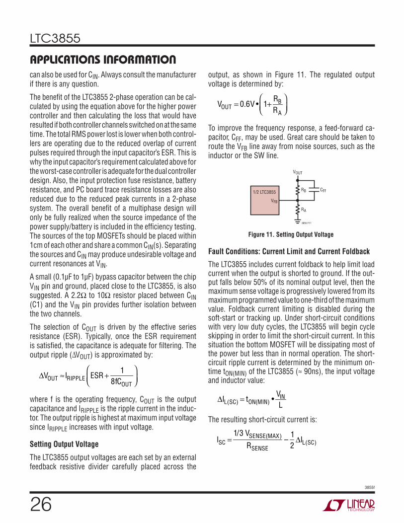
LTC3855
3855f
can also be used for CIN. Always consult the manufacturer if there is any question.
The benefit of the LTC3855 2-phase operation can be cal-culated by using the equation above for the higher power controller and then calculating the loss that would have resulted if both controller channels switched on at the same time. The total RMS power lost is lower when both control-lers are operating due to the reduced overlap of current pulses required through the input capacitor’s ESR. This is why the input capacitor’s requirement calculated above for the worst-case controller is adequate for the dual controller design. Also, the input protection fuse resistance, battery resistance, and PC board trace resistance losses are also reduced due to the reduced peak currents in a 2-phase system. The overall benefit of a multiphase design will only be fully realized when the source impedance of the power supply/battery is included in the efficiency testing. The sources of the top MOSFETs should be placed within 1cm of each other and share a common CIN(s). Separating the sources and CIN may produce undesirable voltage and current resonances at VIN.
A small (0.1µF to 1µF) bypass capacitor between the chip VIN pin and ground, placed close to the LTC3855, is also suggested. A 2.2Ω to 10Ω resistor placed between CIN (C1) and the VIN pin provides further isolation between the two channels.
The selection of COUT is driven by the effective series resistance (ESR). Typically, once the ESR requirement is satisfied, the capacitance is adequate for filtering. The output ripple (∆VOUT) is approximated by:
∆VOUT ≈IRIPPLE ESR + 1
8fCOUT
where f is the operating frequency, COUT is the output capacitance and IRIPPLE is the ripple current in the induc-tor. The output ripple is highest at maximum input voltage since IRIPPLE increases with input voltage.
Setting Output Voltage
The LTC3855 output voltages are each set by an external feedback resistive divider carefully placed across the
output, as shown in Figure 11. The regulated output voltage is determined by:
VOUT = 0.6V • 1+
RBRA
To improve the frequency response, a feed-forward ca-pacitor, CFF, may be used. Great care should be taken to route the VFB line away from noise sources, such as the inductor or the SW line.
applicaTions inForMaTion
Fault Conditions: Current Limit and Current Foldback
The LTC3855 includes current foldback to help limit load current when the output is shorted to ground. If the out-put falls below 50% of its nominal output level, then the maximum sense voltage is progressively lowered from its maximum programmed value to one-third of the maximum value. Foldback current limiting is disabled during the soft-start or tracking up. Under short-circuit conditions with very low duty cycles, the LTC3855 will begin cycle skipping in order to limit the short-circuit current. In this situation the bottom MOSFET will be dissipating most of the power but less than in normal operation. The short-circuit ripple current is determined by the minimum on-time tON(MIN) of the LTC3855 (≈ 90ns), the input voltage and inductor value:
∆IL(SC) = tON(MIN) •
VINL
The resulting short-circuit current is:
ISC =
1/3 VSENSE(MAX)
RSENSE–
12
∆IL(SC)
Figure 11. Setting Output Voltage
1/2 LTC3855
VFB
VOUT
RB CFF
RA
3855 F11
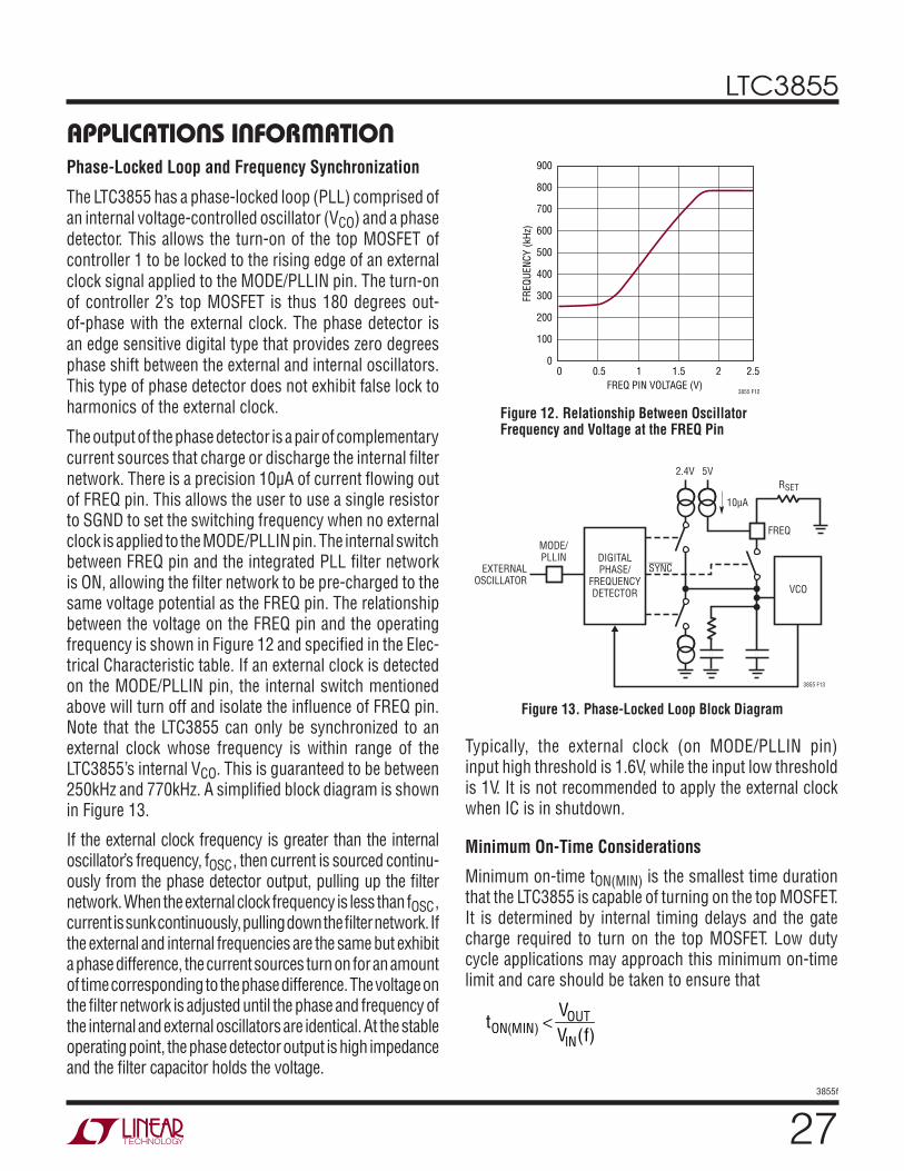
LTC3855
3855f
Phase-Locked Loop and Frequency Synchronization
The LTC3855 has a phase-locked loop (PLL) comprised of an internal voltage-controlled oscillator (VCO) and a phase detector. This allows the turn-on of the top MOSFET of controller 1 to be locked to the rising edge of an external clock signal applied to the MODE/PLLIN pin. The turn-on of controller 2’s top MOSFET is thus 180 degrees out-of-phase with the external clock. The phase detector is an edge sensitive digital type that provides zero degrees phase shift between the external and internal oscillators. This type of phase detector does not exhibit false lock to harmonics of the external clock.
The output of the phase detector is a pair of complementary current sources that charge or discharge the internal filter network. There is a precision 10µA of current flowing out of FREQ pin. This allows the user to use a single resistor to SGND to set the switching frequency when no external clock is applied to the MODE/PLLIN pin. The internal switch between FREQ pin and the integrated PLL filter network is ON, allowing the filter network to be pre-charged to the same voltage potential as the FREQ pin. The relationship between the voltage on the FREQ pin and the operating frequency is shown in Figure 12 and specified in the Elec-trical Characteristic table. If an external clock is detected on the MODE/PLLIN pin, the internal switch mentioned above will turn off and isolate the influence of FREQ pin. Note that the LTC3855 can only be synchronized to an external clock whose frequency is within range of the LTC3855’s internal VCO. This is guaranteed to be between 250kHz and 770kHz. A simplified block diagram is shown in Figure 13.
If the external clock frequency is greater than the internal oscillator’s frequency, fOSC, then current is sourced continu-ously from the phase detector output, pulling up the filter network. When the external clock frequency is less than fOSC, current is sunk continuously, pulling down the filter network. If the external and internal frequencies are the same but exhibit a phase difference, the current sources turn on for an amount of time corresponding to the phase difference. The voltage on the filter network is adjusted until the phase and frequency of the internal and external oscillators are identical. At the stable operating point, the phase detector output is high impedance and the filter capacitor holds the voltage.
Typically, the external clock (on MODE/PLLIN pin) input high threshold is 1.6V, while the input low threshold is 1V. It is not recommended to apply the external clock when IC is in shutdown.
Minimum On-Time Considerations
Minimum on-time tON(MIN) is the smallest time duration that the LTC3855 is capable of turning on the top MOSFET. It is determined by internal timing delays and the gate charge required to turn on the top MOSFET. Low duty cycle applications may approach this minimum on-time limit and care should be taken to ensure that
tON(MIN) <
VOUTVIN(f)
applicaTions inForMaTion
Figure 12. Relationship Between Oscillator Frequency and Voltage at the FREQ Pin
FREQ PIN VOLTAGE (V)0
FREQ
UENC
Y (k
Hz)
0.5 1 1.5 2
3855 F12
2.50
100
300
400
500
900
800
700
200
600
Figure 13. Phase-Locked Loop Block Diagram
DIGITALPHASE/
FREQUENCYDETECTOR
SYNC
VCO
2.4V 5V
10µA
RSET
3855 F13
FREQ
EXTERNALOSCILLATOR
MODE/PLLIN
LTC3855
3855f
If the duty cycle falls below what can be accommodated by the minimum on-time, the controller will begin to skip cycles. The output voltage will continue to be regulated, but the ripple voltage and current will increase.
The minimum on-time for the LTC3855 is approximately 90ns, with reasonably good PCB layout, minimum 30% inductor current ripple and at least 10mV – 15mV ripple on the current sense signal. The minimum on-time can be affected by PCB switching noise in the voltage and current loop. As the peak sense voltage decreases the minimum on-time gradually increases to 130ns. This is of particular concern in forced continuous applications with low ripple current at light loads. If the duty cycle drops below the minimum on-time limit in this situation, a significant amount of cycle skipping can occur with correspondingly larger current and voltage ripple.
Efficiency Considerations
The percent efficiency of a switching regulator is equal to the output power divided by the input power times 100%. It is often useful to analyze individual losses to determine what is limiting the efficiency and which change would produce the most improvement. Percent efficiency can be expressed as:
%Efficiency = 100% – (L1 + L2 + L3 + ...)
where L1, L2, etc. are the individual losses as a percent-age of input power.
Although all dissipative elements in the circuit produce losses, four main sources usually account for most of the losses in LTC3855 circuits: 1) IC VIN current, 2) INTVCC regulator current, 3) I2R losses, 4) Topside MOSFET transition losses.
1. The VIN current is the DC supply current given in the Electrical Characteristics table, which excludes MOSFET driver and control currents. VIN current typi-cally results in a small (<0.1%) loss.
2. INTVCC current is the sum of the MOSFET driver and control currents. The MOSFET driver current results from switching the gate capacitance of the power MOSFETs. Each time a MOSFET gate is switched from low to high to low again, a packet of charge dQ moves
from INTVCC to ground. The resulting dQ/dt is a cur-rent out of INTVCC that is typically much larger than the control circuit current. In continuous mode, IGATECHG = f(QT + QB), where QT and QB are the gate charges of the topside and bottom side MOSFETs.
Supplying INTVCC power through EXTVCC from an out-put-derived source will scale the VIN current required for the driver and control circuits by a factor of (Duty Cycle)/(Efficiency). For example, in a 20V to 5V applica-tion, 10mA of INTVCC current results in approximately 2.5mA of VIN current. This reduces the mid-current loss from 10% or more (if the driver was powered directly from VIN) to only a few percent.
3. I2R losses are predicted from the DC resistances of the fuse (if used), MOSFET, inductor, current sense resistor. In continuous mode, the average output current flows through L and RSENSE, but is “chopped” between the topside MOSFET and the synchronous MOSFET. If the two MOSFETs have approximately the same RDS(ON), then the resistance of one MOSFET can simply be summed with the resistances of L and RSENSE to ob-tain I2R losses. For example, if each RDS(ON) = 10mΩ, RL = 10mΩ, RSENSE = 5mΩ, then the total resistance is 25mΩ. This results in losses ranging from 2% to 8% as the output current increases from 3A to 15A for a 5V output, or a 3% to 12% loss for a 3.3V output. Efficiency varies as the inverse square of VOUT for the same external components and output power level. The combined effects of increasingly lower output voltages and higher currents required by high performance digital systems is not doubling but quadrupling the importance of loss terms in the switching regulator system!
4. Transition losses apply only to the topside MOSFET(s), and become significant only when operating at high input voltages (typically 15V or greater). Transition losses can be estimated from:
Transition Loss = (1.7) VIN2 IO(MAX) CRSS f
Other “hidden” losses such as copper trace and internal battery resistances can account for an additional 5% to 10% efficiency degradation in portable systems. It is very important to include these “system” level losses during the design phase. The internal battery and fuse resistance
applicaTions inForMaTion
LTC3855
3855f
losses can be minimized by making sure that CIN has adequate charge storage and very low ESR at the switch- ing frequency. A 25W supply will typically require a minimum of 20µF to 40µF of capacitance having a maximum of 20mΩ to 50mΩ of ESR. The LTC3855 2-phase architecture typically halves this input capacitance requirement over competing solutions. Other losses including Schottky conduction losses during dead time and inductor core losses generally account for less than 2% total additional loss.
Modest improvements in Burst Mode efficiency may be realized by using a smaller inductor value, a lower switch-ing frequency or for DCR sensing applications, making the DCR filter’s time constant smaller than the L/DCR time constant for the inductor. A small Schottky diode with a current rating equal to about 20% of the maximum load current or less may yield minor improvements, too.
Checking Transient Response
The regulator loop response can be checked by looking at the load current transient response. Switching regulators take several cycles to respond to a step in DC (resistive) load current. When a load step occurs, VOUT shifts by an amount equal to ∆ILOAD (ESR), where ESR is the effective series resistance of COUT. ∆ILOAD also begins to charge or discharge COUT generating the feedback error signal that forces the regulator to adapt to the current change and return VOUT to its steady-state value. During this recovery time VOUT can be monitored for excessive overshoot or ringing, which would indicate a stability problem. The availability of the ITH pin not only allows optimization of control loop behavior but also provides a DC coupled and AC filtered closed loop response test point. The DC step, rise time and settling at this test point truly reflects the closed loop response. Assuming a predominantly second order system, phase margin and/or damping factor can be estimated using the percentage of overshoot seen at this pin. The bandwidth can also be estimated by examining the rise time at the pin. The ITH external components shown in the Typical Application circuit will provide an adequate starting point for most applications.
The ITH series RC-CC filter sets the dominant pole-zero loop compensation. The values can be modified slightly (from 0.5 to 2 times their suggested values) to optimize transient response once the final PC layout is done and the particular output capacitor type and value have been determined. The output capacitors need to be selected because the various types and values determine the loop gain and phase. An output current pulse of 20% to 80% of full-load current having a rise time of 1µs to 10µs will produce output voltage and ITH pin waveforms that will give a sense of the overall loop stability without break-ing the feedback loop. Placing a power MOSFET directly across the output capacitor and driving the gate with an appropriate signal generator is a practical way to produce a realistic load step condition. The initial output voltage step resulting from the step change in output current may not be within the bandwidth of the feedback loop, so this signal cannot be used to determine phase margin. This is why it is better to look at the ITH pin signal which is in the feedback loop and is the filtered and compensated control loop response. The gain of the loop will be in-creased by increasing RC and the bandwidth of the loop will be increased by decreasing CC. If RC is increased by the same factor that CC is decreased, the zero frequency will be kept the same, thereby keeping the phase shift the same in the most critical frequency range of the feedback loop. The output voltage settling behavior is related to the stability of the closed-loop system and will demonstrate the actual overall supply performance.
A second, more severe transient is caused by switching in loads with large (>1µF) supply bypass capacitors. The discharged bypass capacitors are effectively put in parallel with COUT, causing a rapid drop in VOUT. No regulator can alter its delivery of current quickly enough to prevent this sudden step change in output voltage if the load switch resistance is low and it is driven quickly. If the ratio of CLOAD to COUT is greater than 1:50, the switch rise time should be controlled so that the load rise time is limited to approximately 25 • CLOAD. Thus a 10µF capacitor would require a 250µs rise time, limiting the charging current to about 200mA.
applicaTions inForMaTion
LTC3855
03855f
PC Board Layout Checklist
When laying out the printed circuit board, the following checklist should be used to ensure proper operation of the IC. These items are also illustrated graphically in the layout diagram of Figure 14. Figure 15 illustrates the current waveforms present in the various branches of the 2-phase synchronous regulators operating in the continuous mode. Check the following in your layout:
1. Are the top N-channel MOSFETs M1 and M3 located within 1 cm of each other with a common drain con- nection at CIN? Do not attempt to split the input de-coupling for the two channels as it can cause a large resonant loop.
2. Are the signal and power grounds kept separate? The combined IC signal ground pin and the ground return of CINTVCC must return to the combined COUT (–) ter-minals. The VFB and ITH traces should be as short as possible. The path formed by the top N-channel MOSFET, Schottky diode and the CIN capacitor should have short leads and PC trace lengths. The output capacitor (–) terminals should be connected as close as possible to the (–) terminals of the input capacitor by placing the capacitors next to each other and away from the Schottky loop described above.
3. Do the LTC3855 VFB pins’ resistive dividers connect to the (+) terminals of COUT? The resistive divider must be connected between the (+) terminal of COUT and signal ground. The feedback resistor connections should not be along the high current input feeds from the input capacitor(s).
4. Are the SENSE+ and SENSE– leads routed together with minimum PC trace spacing? The filter capacitor between SENSE+ and SENSE– should be as close as possible to the IC. Ensure accurate current sensing with Kelvin connections at the sense resistor or inductor, whichever is used for current sensing.
5. Is the INTVCC decoupling capacitor connected close to the IC, between the INTVCC and the power ground pins? This capacitor carries the MOSFET drivers current peaks. An additional 1µF ceramic capacitor placed immediately next to the INTVCC and PGND pins can help improve noise performance substantially.
6. Keep the switching nodes (SW1, SW2), top gate nodes (TG1, TG2), and boost nodes (BOOST1, BOOST2) away from sensitive small-signal nodes, especially from the opposite channel’s voltage and current sensing feed-back pins. All of these nodes have very large and fast moving signals and therefore should be kept on the “output side” of the LTC3855 and occupy minimum PC trace area. If DCR sensing is used, place the top resistor (Figure 2b, R1) close to the switching node.
7. Are DIFFP and DIFFN leads routed together and correctly Kelvin sensing the output voltage?
8. Use a modified “star ground” technique: a low imped-ance, large copper area central grounding point on the same side of the PC board as the input and output capacitors with tie-ins for the bottom of the INTVCC decoupling capacitor, the bottom of the voltage feedback resistive divider and the SGND pin of the IC.
PC Board Layout Debugging
Start with one controller at a time. It is helpful to use a DC-50MHz current probe to monitor the current in the inductor while testing the circuit. Monitor the output switching node (SW pin) to synchronize the oscilloscope to the internal oscillator and probe the actual output voltage as well. Check for proper performance over the operating voltage and current range expected in the application. The frequency of operation should be maintained over the input voltage range down to dropout and until the output load drops below the low current operation threshold—typically 10% of the maximum designed cur-rent level in Burst Mode operation.
The duty cycle percentage should be maintained from cycle to cycle in a well-designed, low noise PCB implemen-tation. Variation in the duty cycle at a subharmonic rate can suggest noise pickup at the current or voltage sensing inputs or inadequate loop compensation. Overcompensa-tion of the loop can be used to tame a poor PC layout if regulator bandwidth optimization is not required. Only after each controller is checked for its individual performance should both controllers be turned on at the same time. A particularly difficult region of operation is when one controller channel is nearing its current comparator trip point when the other channel is turning on its top MOSFET.
applicaTions inForMaTion
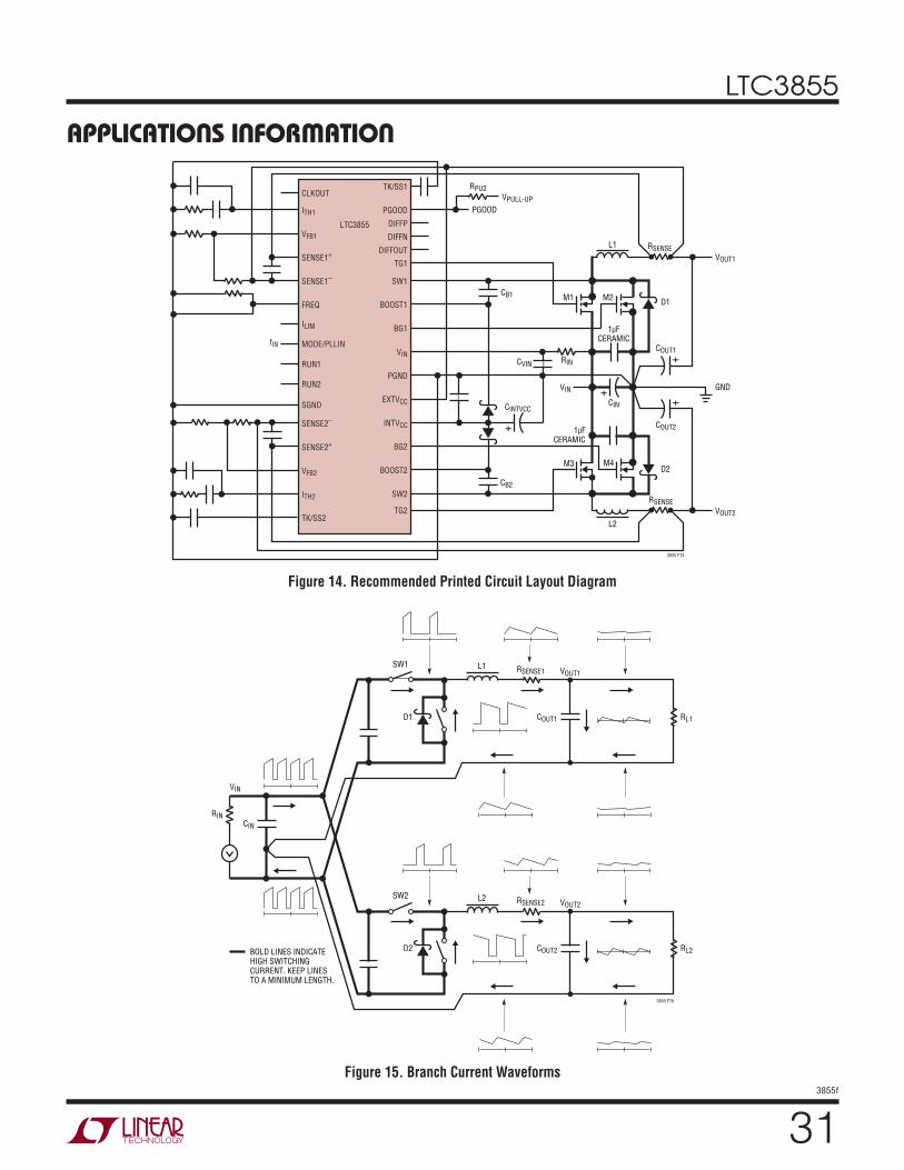
LTC3855
3855f
Figure 15. Branch Current Waveforms
RL1D1
L1SW1 RSENSE1 VOUT1
COUT1
VIN
CIN
RIN
RL2D2BOLD LINES INDICATEHIGH SWITCHING CURRENT. KEEP LINESTO A MINIMUM LENGTH.
L2SW2
3855 F15
RSENSE2 VOUT2
COUT2
Figure 14. Recommended Printed Circuit Layout Diagram
CB2
CB1
CINTVCC
+
CIN
D1
1µFCERAMIC
M1 M2
M3 M4D2
+
CVIN
VIN
RIN
L1
L2
COUT1
VOUT1
GND
VOUT2
3855 F14
+
COUT2
+
RSENSE
RSENSE
RPU2
PGOODVPULL-UP
fIN
1µFCERAMIC
ITH1
VFB1
SENSE1+
SENSE1–
FREQ
SENSE2–
SENSE2+
VFB2
ITH2
TK/SS2
TK/SS1
PGOOD
SW1
BOOST1
BG1
VIN
PGND
EXTVCC
INTVCC
BG2
BOOST2
SW2
TG2
SGND
ILIM
MODE/PLLIN
RUN1
RUN2
CLKOUT
LTC3855
DIFFOUT
TG1
DIFFN
DIFFP
applicaTions inForMaTion
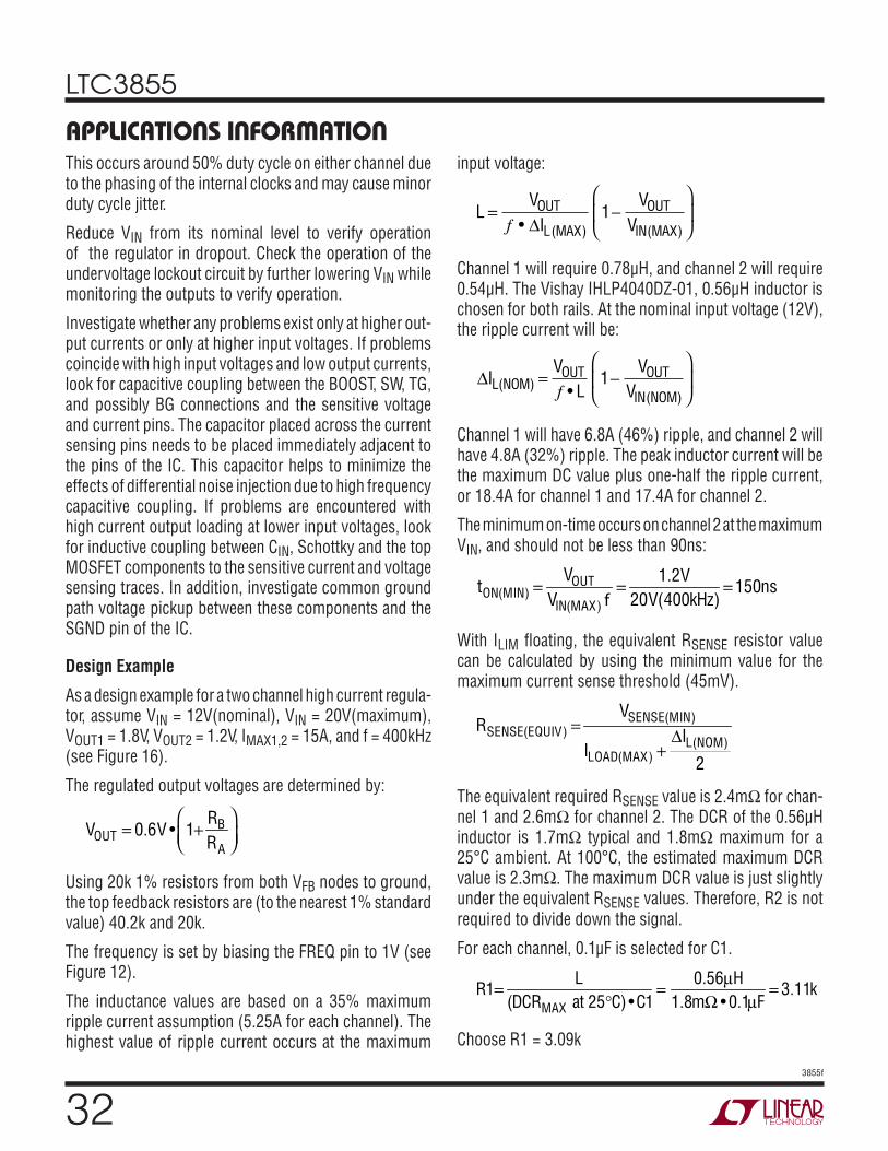
LTC3855
3855f
This occurs around 50% duty cycle on either channel due to the phasing of the internal clocks and may cause minor duty cycle jitter.
Reduce VIN from its nominal level to verify operation of the regulator in dropout. Check the operation of the undervoltage lockout circuit by further lowering VIN while monitoring the outputs to verify operation.
Investigate whether any problems exist only at higher out-put currents or only at higher input voltages. If problems coincide with high input voltages and low output currents, look for capacitive coupling between the BOOST, SW, TG, and possibly BG connections and the sensitive voltage and current pins. The capacitor placed across the current sensing pins needs to be placed immediately adjacent to the pins of the IC. This capacitor helps to minimize the effects of differential noise injection due to high frequency capacitive coupling. If problems are encountered with high current output loading at lower input voltages, look for inductive coupling between CIN, Schottky and the top MOSFET components to the sensitive current and voltage sensing traces. In addition, investigate common ground path voltage pickup between these components and the SGND pin of the IC.
Design Example
As a design example for a two channel high current regula-tor, assume VIN = 12V(nominal), VIN = 20V(maximum), VOUT1 = 1.8V, VOUT2 = 1.2V, IMAX1,2 = 15A, and f = 400kHz (see Figure 16).
The regulated output voltages are determined by:
VOUT = 0.6V • 1+
RBRA
Using 20k 1% resistors from both VFB nodes to ground, the top feedback resistors are (to the nearest 1% standard value) 40.2k and 20k.
The frequency is set by biasing the FREQ pin to 1V (see Figure 12).
The inductance values are based on a 35% maximum ripple current assumption (5.25A for each channel). The highest value of ripple current occurs at the maximum
input voltage:
LV
IV
VOUT
L MAX
OUT
IN MAX= −
f • ( ) ( )∆
1
Channel 1 will require 0.78µH, and channel 2 will require 0.54µH. The Vishay IHLP4040DZ-01, 0.56µH inductor is chosen for both rails. At the nominal input voltage (12V), the ripple current will be:
∆IV
LV
VL NOMOUT OUT
IN NOM( )
( )•= −
f
1
Channel 1 will have 6.8A (46%) ripple, and channel 2 will have 4.8A (32%) ripple. The peak inductor current will be the maximum DC value plus one-half the ripple current, or 18.4A for channel 1 and 17.4A for channel 2.
The minimum on-time occurs on channel 2 at the maximum VIN, and should not be less than 90ns:
tON(MIN) =
VOUTVIN(MAX) f
= 1.2V20V(400kHz)
= 150ns
With ILIM floating, the equivalent RSENSE resistor value can be calculated by using the minimum value for the maximum current sense threshold (45mV).
RSENSE(EQUIV) =VSENSE(MIN)
ILOAD(MAX) +∆IL(NOM)
2
The equivalent required RSENSE value is 2.4mΩ for chan-nel 1 and 2.6mΩ for channel 2. The DCR of the 0.56µH inductor is 1.7mΩ typical and 1.8mΩ maximum for a 25°C ambient. At 100°C, the estimated maximum DCR value is 2.3mΩ. The maximum DCR value is just slightly under the equivalent RSENSE values. Therefore, R2 is not required to divide down the signal.
For each channel, 0.1µF is selected for C1.
R1= L
(DCRMAX at 25°C) •C1= 0.56µH
1.8mΩ • 0.1µF= 3.11k
Choose R1 = 3.09k
applicaTions inForMaTion
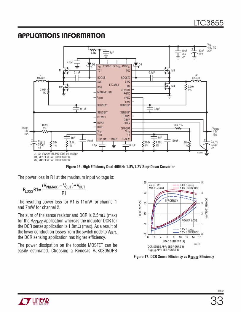
LTC3855
3855f
applicaTions inForMaTion
The power loss in R1 at the maximum input voltage is:
PLOSSR1=
(VIN(MAX) − VOUT ) • VOUT
R1
The resulting power loss for R1 is 11mW for channel 1 and 7mW for channel 2.
The sum of the sense resistor and DCR is 2.5mΩ (max) for the RSENSE application whereas the inductor DCR for the DCR sense application is 1.8mΩ (max). As a result of the lower conduction losses from the switch node to VOUT, the DCR sensing application has higher efficiency.
The power dissipation on the topside MOSFET can be easily estimated. Choosing a Renesas RJK0305DPB
Figure 17. DCR Sense Efficiency vs RSENSE Efficiency
LOAD CURRENT (A)0
85
EFFI
CIEN
CY (%
)
POWER LOSS (W
)
90
161412108642
80
75
70
95
4
3
2
1
0
5
3855 F17
1.2V RSENSE1.2V DCR SENSE
1.8V RSENSE1.8V DCR SENSE
VIN = 12VMODE = CCM
DCR SENSE APP: SEE FIGURE 16RSENSE APP: SEE FIGURE 19
EFFICIENCY
POWER LOSS
Figure 16. High Efficiency Dual 400kHz 1.8V/1.2V Step-Down Converter
D3 D4
M1
M2
0.1µF
40.2k1%
L10.56µH
3.09k1%
1nF150pF
0.1µF 0.1µF
82µF25V
COUT1330µF
2
L1, L2: VISHAY IHLP4040DZ-01, 0.56µHM1, M3: RENESAS RJK0305DPBM2, M4: RENESAS RJK0330DPB
20k1%
12.1k1%
VOUT11.8V15A
M3
M4
0.1µFL2
0.56µH
1nF150pF COUT2
330µF2
20k1%
4.99k1%
100k1%
VOUT21.2V15A
TG1 TG2
BOOST1 BOOST2SW1 SW2
BG1 BG2
SGND
PGNDFREQ
SENSE1+ SENSE2+
DIFFP
SENSE1– SENSE2–
VFB1 VFB2ITH1 ITH2
VIN PGOOD INTVCC
TK/SS1 TK/SS2
VIN4.5V TO 20V
3855 F16
EXTVCC
0.1µF 0.1µF
LTC3855
MODE/PLLIN
ILIM1
ITEMP1 ITEMP2
ILIM2
DIFFN
DIFFOUT
CLKOUT
RUN1RUN2
3.09k1%
4.7µF
1µF2.2Ω
+
+10µF25V
2
+
20k, 1%
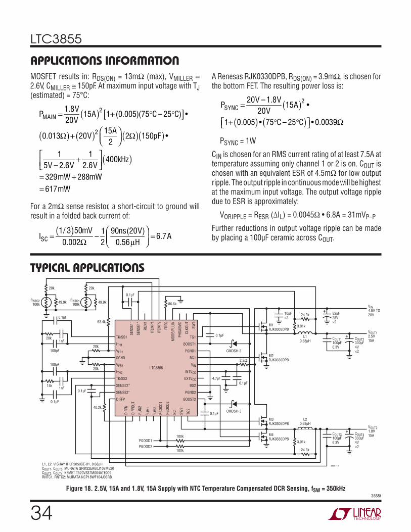
LTC3855
3855f
applicaTions inForMaTionMOSFET results in: RDS(ON) = 13mΩ (max), VMILLER = 2.6V, CMILLER ≅ 150pF. At maximum input voltage with TJ (estimated) = 75°C:
PMAIN = 1.8V20V
15A( )2 1+ (0.005)(75°C – 25°C)[ ] •
0.013Ω( ) + 20V( )2 15A2
2Ω( ) 150pF( ) •
15V – 2.6V
+ 12.6V
400kHz( )= 329mW + 288mW= 617mW
For a 2mΩ sense resistor, a short-circuit to ground will result in a folded back current of:
ISC =
1/ 3( )50mV0.002Ω
–12
90ns(20V)0.56µH
= 6.7A
A Renesas RJK0330DPB, RDS(ON) = 3.9mΩ, is chosen for the bottom FET. The resulting power loss is:
PSYNC = 20V – 1.8V20V
15A( )2 •
1+ 0.005( ) • 75°C – 25°C( ) • 0.0039Ω
PSYNC = 1W
CIN is chosen for an RMS current rating of at least 7.5A at temperature assuming only channel 1 or 2 is on. COUT is chosen with an equivalent ESR of 4.5mΩ for low output ripple. The output ripple in continuous mode will be highest at the maximum input voltage. The output voltage ripple due to ESR is approximately:
VORIPPLE = RESR (∆IL) = 0.0045Ω • 6.8A = 31mVP–P
Further reductions in output voltage ripple can be made by placing a 100µF ceramic across COUT.
L1, L2: VISHAY IHLP5050CE-01, 0.68µHCOUT1, COUT3: MURATA GRM32ER60J107ME20COUT2, COUT4: KEMET T520V337M004ATE009RNTC1, RNTC2: MURATA NCP18WF104J03RB
3855 F18
TG1
BOOST1
PGND1
BG1
VIN
INTVCC
EXTVCC
BG2
PGND2
BOOST2
TK/SS1
ITH1
VFB1
SGND
VFB2
ITH2
TK/SS2
SENSE2+
SENSE2–
DIFFP
20k
0.1µF
40.2k
SENS
E1–
SENS
E1+
RUN1
ITEM
P1
ITEM
P2
FREQ
MOD
E/PL
LIN
PHSA
SMD
CLKO
UT
SW1
DIFF
N
DIFF
OUT
RUN2
I LIM
1
I LIM
2
PGOO
D1
PGOO
D2
PGOOD1PGOOD2
NC SW2
TG2
63.4k
49.9kRNTC1100k
20k
86.6k
100k
100k
20k
2.2Ω
4.7µF
0.1µF
0.1µF
LTC3855
1nF20k
0.1µF
100pF
10µF2
82µF25V
2
1nF15k
0.1µF
100pF
0.1µF
49.9kRNTC2100k
20k
CMDSH-3
M4RJK0330DPB
M3RJK0305DPB
M2RJK0330DPB
M1RJK0305DPB
CMDSH-3
0.1µF
L10.68µH
L20.68µH
24.9k
24.9k
3.01k
3.01k
VOUT21.8V15A
VIN4.5V TO 20V
VOUT12.5V15A
+
COUT1100µF6.3V
COUT2330µF4V
2
+
COUT3100µF6.3V
COUT4330µF4V
2
+
Figure 18. 2.5V, 15A and 1.8V, 15A Supply with NTC Temperature Compensated DCR Sensing, fSW = 350kHz
Typical applicaTions
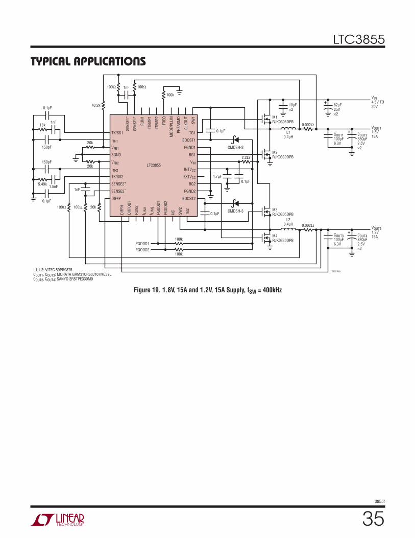
LTC3855
3855f
Typical applicaTions
Figure 19. 1.8V, 15A and 1.2V, 15A Supply, fSW = 400kHz
L1, L2: VITEC 59PR9875COUT1, COUT3: MURATA GRM31CR60J107ME39LCOUT2, COUT4: SANYO 2R5TPE330M9
3855 F19
TG1
BOOST1
PGND1
BG1
VIN
INTVCC
EXTVCC
BG2
PGND2
BOOST2
TK/SS1
ITH1
VFB1
SGND
VFB2
ITH2
TK/SS2
SENSE2+
SENSE2–
DIFFP
20k
1nF
20k
SENS
E1–
SENS
E1+
RUN1
ITEM
P1
ITEM
P2
FREQ
MOD
E/PL
LIN
PHSA
SMD
CLKO
UT
SW1
DIFF
N
DIFF
OUT
RUN2
I LIM
1
I LIM
2
PGOO
D1
PGOO
D2
PGOOD1PGOOD2
NC SW2
TG2
40.2k
100k
100k
100k
20k
2.2Ω
4.7µF
0.1µF
0.1µF
LTC3855
1nF18k
0.1µF
150pF
10µF2
82µF25V
2
1.5nF5.49k
0.1µF
150pF
1nF
CMDSH-3
M4RJK0330DPB
M3RJK0305DPB
M2RJK0330DPB
M1RJK0305DPB
CMDSH-3
0.1µF
L10.4µH
L20.4µH
0.002Ω
0.002Ω VOUT21.2V15A
VIN4.5V TO 20V
VOUT11.8V15A
+
COUT1100µF6.3V
COUT2330µF2.5V
2
+
COUT3100µF6.3V
COUT4330µF2.5V
2
+
100Ω100Ω
100Ω100Ω

LTC3855
3855f
Typical applicaTions
Figure 20. High Efficiency Dual Phase 1.2V, 40A Supply, fSW = 250kHz
L1, L2: PULSE PA0513.441NLTCOUT1: MURATA GRM31CR60J107ME39LCOUT2: SANYO 2R5TPE330M9
3855 F20
TG1
BOOST1
PGND1
BG1
VIN
INTVCC
EXTVCC
BG2
PGND2
BOOST2
TK/SS1
ITH1
VFB1
SGND
VFB2
ITH2
TK/SS2
SENSE2+
SENSE2–
DIFFP
20k
1nF20k
SENS
E1–
SENS
E1+
RUN1
ITEM
P1
ITEM
P2
FREQ
MOD
E/PL
LIN
PHSA
SMD
CLKO
UT
SW1
DIFF
N
DIFF
OUT
RUN2
I LIM
1
I LIM
2
PGOO
D1
PGOO
D2
PGOOD
NC SW2
TG2
5.9k
100Ω
250kHzRUN
RUN
100Ω
100k
2.2Ω
4.7µF
0.1µF
0.1µF
LTC3855
10µF4
270µF16V
100pF
2200pF
1nF
CMDSH-3
M4RJK0330DPB
2
M3RJK0305DPB
M2RJK0330DPB
2
M1RJK0305DPB
CMDSH-3
0.1µF
L10.44µH
L20.44µH
0.001Ω1%
0.001Ω1%
VIN4.5V TO 14V
VOUT1.2V40A
+
COUT1100µF6.3V
4
COUT2330µF2.5V
4
+
100Ω100Ω
0.1µF
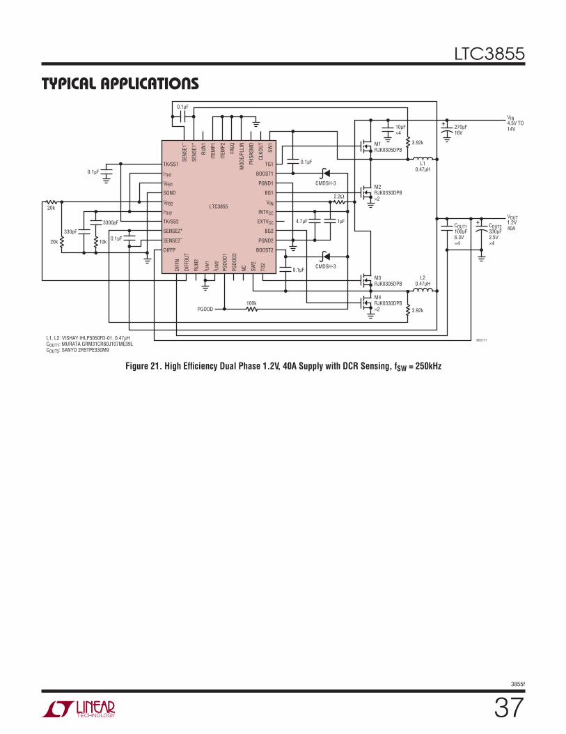
LTC3855
3855f
Figure 21. High Efficiency Dual Phase 1.2V, 40A Supply with DCR Sensing, fSW = 250kHz
L1, L2: VISHAY IHLP5050FD-01, 0.47µHCOUT1: MURATA GRM31CR60J107ME39LCOUT2: SANYO 2R5TPE330M9
3855 F21
TG1
BOOST1
PGND1
BG1
VIN
INTVCC
EXTVCC
BG2
PGND2
BOOST2
TK/SS1
ITH1
VFB1
SGND
VFB2
ITH2
TK/SS2
SENSE2+
SENSE2–
DIFFP
20k
0.1µF20k
SENS
E1–
SENS
E1+
RUN1
ITEM
P1
ITEM
P2
FREQ
MOD
E/PL
LIN
PHSA
SMD
CLKO
UT
SW1
DIFF
N
DIFF
OUT
RUN2
I LIM
1
I LIM
2
PGOO
D1
PGOO
D2
PGOOD
NC SW2
TG2
10k
100k
2.2Ω
4.7µF
0.1µF
0.1µF
LTC3855
10µF4
270µF16V
330pF
3300pF
0.1µF
CMDSH-3
M4RJK0330DPB
2
M3RJK0305DPB
M2RJK0330DPB
2
M1RJK0305DPB
CMDSH-3
1µF
L10.47µH
L20.47µH
3.92k
3.92k
VIN4.5V TO 14V
VOUT1.2V40A
+
COUT1100µF6.3V
4
COUT2330µF2.5V
4
+
0.1µF
Typical applicaTions
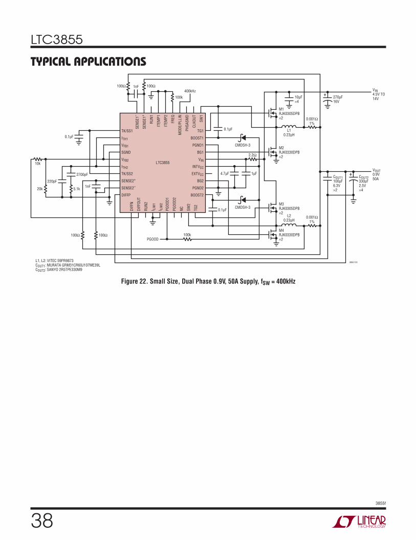
LTC3855
3855f
Typical applicaTions
Figure 22. Small Size, Dual Phase 0.9V, 50A Supply, fSW = 400kHz
L1, L2: VITEC 59PR9873COUT1: MURATA GRM31CR60J107ME39LCOUT2: SANYO 2R5TPE330M9
3855 F22
TG1
BOOST1
PGND1
BG1
VIN
INTVCC
EXTVCC
BG2
PGND2
BOOST2
TK/SS1
ITH1
VFB1
SGND
VFB2
ITH2
TK/SS2
SENSE2+
SENSE2–
DIFFP
10k
1nF20k
SENS
E1–
SENS
E1+
RUN1
ITEM
P1
ITEM
P2
FREQ
MOD
E/PL
LIN
PHSA
SMD
CLKO
UT
SW1
DIFF
N
DIFF
OUT
RUN2
I LIM
1
I LIM
2
PGOO
D1
PGOO
D2
PGOOD
NC SW2
TG2
5.1k
100Ω400kHz
100k
100Ω
100k
2.2Ω
4.7µF
0.1µF
0.1µF
LTC3855
10µF4
270µF16V
220pF
2700pF
1nF
CMDSH-3
M4RJK0330DPB
2
M3RJK0305DPB
2
M2RJK0330DPB
2
M1RJK0305DPB
2
CMDSH-3
1µF
L10.23µH
L20.23µH
0.001Ω1%
0.001Ω1%
VIN4.5V TO 14V
VOUT0.9V50A
+
COUT1100µF6.3V
2
COUT2330µF2.5V
4
+
100Ω100Ω
0.1µF
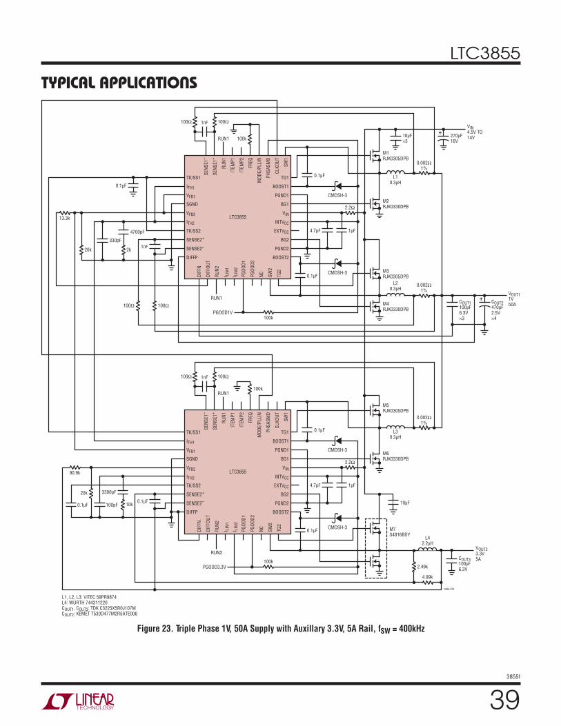
LTC3855
3855f
Typical applicaTions
Figure 23. Triple Phase 1V, 50A Supply with Auxillary 3.3V, 5A Rail, fSW = 400kHz
TG1
BOOST1
PGND1
BG1
VIN
INTVCC
EXTVCC
BG2
PGND2
BOOST2
TK/SS1
ITH1
VFB1
SGND
VFB2
ITH2
TK/SS2
SENSE2+
SENSE2–
DIFFP
13.3k
1nF20k
SENS
E1–
SENS
E1+
RUN1
ITEM
P1
ITEM
P2
FREQ
MOD
E/PL
LIN
PHSA
SMD
CLKO
UT
SW1
DIFF
N
DIFF
OUT
RUN2
I LIM
1
I LIM
2
PGOO
D1
PGOO
D2
PGOOD1V
NC SW2
TG2
2k
100Ω
100kRUN1
RUN1
RUN2
100Ω
100k
2.2Ω
4.7µF
0.1µF
0.1µF
LTC3855
10µF3
270µF16V
330pF
4700pF
1nF
CMDSH-3
M4RJK0330DPB
M3RJK0305DPB
M2RJK0330DPB
M1RJK0305DPB
CMDSH-3
1µF
L10.3µH
L20.3µH
0.002Ω1%
0.002Ω1%
VIN4.5V TO 14V
VOUT11V50A
+
COUT1100µF6.3V
3
COUT2470µF2.5V
4
+100Ω100Ω
0.1µF
L1, L2, L3: VITEC 59PR9874L4: WURTH 744311220COUT1, COUT3: TDK C3225X5R0J107MCOUT2: KEMET T530D477M2R5ATE006
3855 F23
TG1
BOOST1
PGND1
BG1
VIN
INTVCC
EXTVCC
BG2
PGND2
BOOST2
TK/SS1
ITH1
VFB1
SGND
VFB2
ITH2
TK/SS2
SENSE2+
SENSE2–
DIFFP
90.9k
0.1µF
20k
SENS
E1–
SENS
E1+
RUN1
ITEM
P1
ITEM
P2
FREQ
MOD
E/PL
LIN
PHSA
SMD
CLKO
UT
SW1
DIFF
N
DIFF
OUT
RUN2
I LIM
1
I LIM
2
PGOO
D1
PGOO
D2
PGOOD3.3V
NC SW2
TG2
10k
100Ω
RUN1100k
100Ω
100k
2.2Ω
4.7µF
0.1µF
0.1µF
LTC3855
100pF0.1µF
3300pF
1nF
CMDSH-3 M7S4816BDY
M6RJK0330DPB
M5RJK0305DPB
CMDSH-3
1µF
L30.3µH
0.002Ω1%
VOUT23.3V5ACOUT3
100µF6.3V
L42.2µH
4.99k
2.49k
10µF
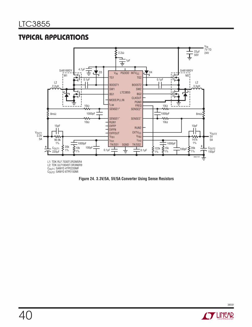
LTC3855
03855f
0.1µF
90.9k1%
L22.2µH
1000pF
1000pF 1000pF
22µF50V
20k1%
10k1%
VOUT13.3V
5A
0.1µF
147k1%
L23.3µH
1000pF
COUT2150µF
20k1%
15k1%
122k1%
VOUT25V5A
TG1 TG2
BOOST1 BOOST2SW1 SW2
BG1 BG2
SGND
PGNDFREQ
SENSE1+ SENSE2+
RUN2
EXTVCC
SENSE1– SENSE2–
VFB1 VFB2ITH1 ITH2
VIN PGOOD INTVCC
TK/SS1 TK/SS2
VIN7V TO 24V
3855 F24
0.1µF100pF
0.1µF
LTC3855
MODE/PLLINILIM
CLKOUT
RUN1DIFFPDIFFNDIFFOUT
4.7µF
+COUT1220µF
+
10pF15pF
100pF
10Ω
10Ω
10Ω
10Ω
2.2Ω
1µF
D4D3
L1: TDK RLF 7030T-2R2M5R4L2: TDK ULF10045T-3R3N6R9COUT1: SANYO 4TPE220MFCOUT2: SANYO 6TPE150MI
8mΩ 8mΩ
M1 M2
Si4816BDYSi4816BDY
Typical applicaTions
Figure 24. 3.3V/5A, 5V/5A Converter Using Sense Resistors
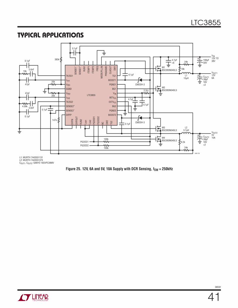
LTC3855
3855f
Typical applicaTions
L1: WURTH 7443551131L2: WURTH 7443551370COUT1, COUT2: SANYO 16SVPC39MV
3855 F25
TG1
BOOST1
PGND1
BG1
VIN
INTVCC
EXTVCC
BG2
PGND2
BOOST2
TK/SS1
ITH1
VFB1
SGND
VFB2
ITH2
TK/SS2
SENSE2+
SENSE2–
DIFFP
20k
0.1µF
147k
SENS
E1–
SENS
E1+
RUN1
ITEM
P1
ITEM
P2
FREQ
MOD
E/PL
LIN
PHSA
SMD
CLKO
UT
SW1
DIFF
N
DIFF
OUT
RUN2
I LIM
1
I LIM
2
PGOO
D1
PGOO
D2
PGOOD1
PGOOD2
NC SW2
TG2
383k
100k
100k
20k
2.2Ω
4.7µF
0.1µF
0.1µF
LTC3855
5.6nF10k
47pF
4.7µF6
100µF50V
5.6nF4.99k
0.1µF
0.1µF
47pF
0.1µF
CMDSH-3
M4BSC093N040LS
M3BSC093N040LS
M2BSC093N040LS
M1BSC093N040LS
CMDSH-3
0.1µF
L113µH
L23.7µH
24k
24k
18k
8.2k
VOUT25V10A
VIN13V TO 38V
VOUT112V6A
+
COUT139µF16V
2
+
COUT239µF16V
2
+
Figure 25. 12V, 6A and 5V, 10A Supply with DCR Sensing, fSW = 250kHz
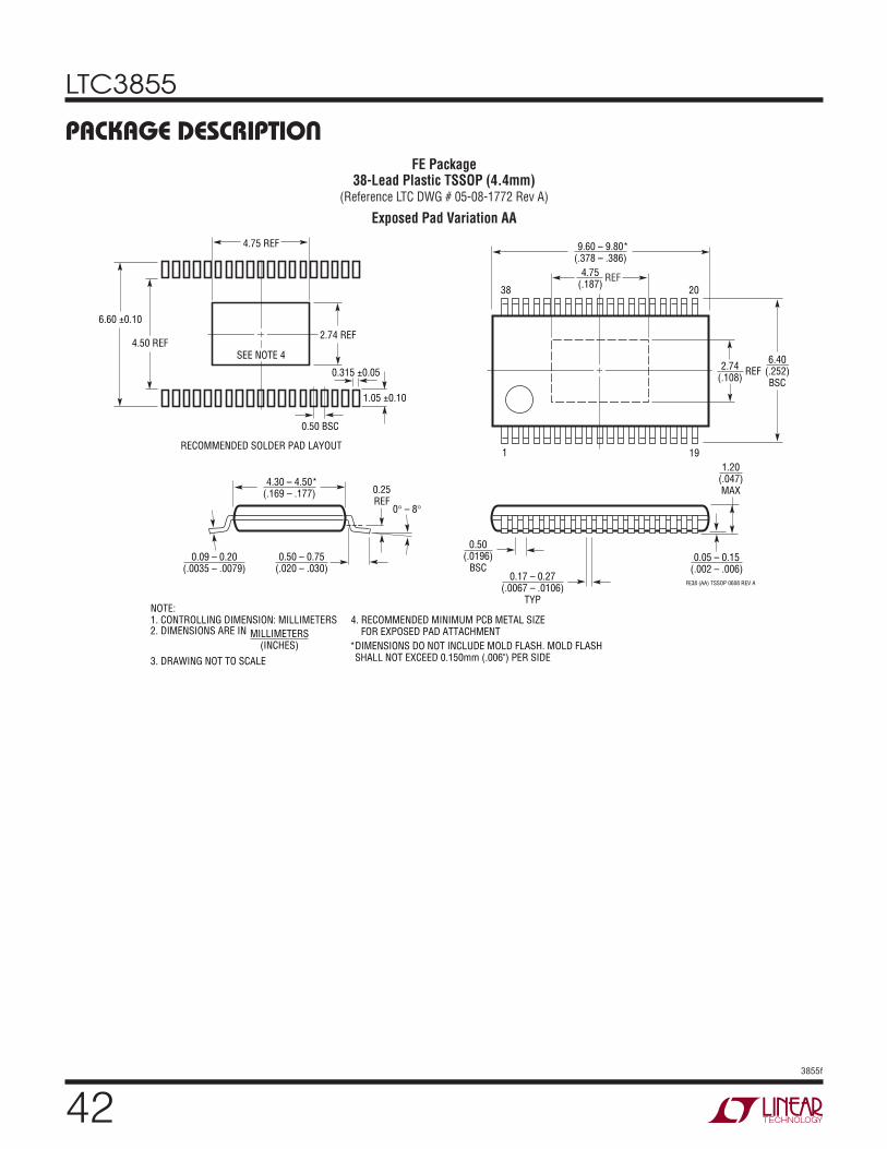
LTC3855
3855f
package DescripTionFE Package
38-Lead Plastic TSSOP (4.4mm)(Reference LTC DWG # 05-08-1772 Rev A)
Exposed Pad Variation AA
4.75(.187)
REF
FE38 (AA) TSSOP 0608 REV A
0.09 – 0.20(.0035 – .0079)
0 – 8
0.25REF
0.50 – 0.75(.020 – .030)
4.30 – 4.50*(.169 – .177)
1 19
20
REF
9.60 – 9.80*(.378 – .386)
38
1.20(.047)MAX
0.05 – 0.15(.002 – .006)
0.50(.0196)
BSC0.17 – 0.27
(.0067 – .0106)TYP
RECOMMENDED SOLDER PAD LAYOUT
0.315 ±0.05
0.50 BSC
4.50 REF
6.60 ±0.10
1.05 ±0.10
4.75 REF
2.74 REF
2.74(.108)
MILLIMETERS(INCHES) *DIMENSIONS DO NOT INCLUDE MOLD FLASH. MOLD FLASH
SHALL NOT EXCEED 0.150mm (.006") PER SIDE
NOTE:1. CONTROLLING DIMENSION: MILLIMETERS2. DIMENSIONS ARE IN
3. DRAWING NOT TO SCALE
SEE NOTE 4
4. RECOMMENDED MINIMUM PCB METAL SIZE FOR EXPOSED PAD ATTACHMENT
6.40(.252)BSC
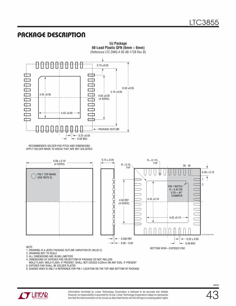
LTC3855
3855f
Information furnished by Linear Technology Corporation is believed to be accurate and reliable. However, no responsibility is assumed for its use. Linear Technology Corporation makes no representa-tion that the interconnection of its circuits as described herein will not infringe on existing patent rights.
package DescripTion
6.00 ± 0.10(4 SIDES)
NOTE:1. DRAWING IS A JEDEC PACKAGE OUTLINE VARIATION OF (WJJD-2)2. DRAWING NOT TO SCALE3. ALL DIMENSIONS ARE IN MILLIMETERS4. DIMENSIONS OF EXPOSED PAD ON BOTTOM OF PACKAGE DO NOT INCLUDE MOLD FLASH. MOLD FLASH, IF PRESENT, SHALL NOT EXCEED 0.20mm ON ANY SIDE, IF PRESENT5. EXPOSED PAD SHALL BE SOLDER PLATED6. SHADED AREA IS ONLY A REFERENCE FOR PIN 1 LOCATION ON THE TOP AND BOTTOM OF PACKAGE
PIN 1 TOP MARK(SEE NOTE 6)
PIN 1 NOTCHR = 0.45 OR
0.35 45°CHAMFER
0.40 ± 0.10
4039
1
2
BOTTOM VIEW—EXPOSED PAD
4.50 REF(4-SIDES)
4.42 ±0.10
4.42 ±0.10
4.42 ±0.05
4.42 ±0.05
0.75 ± 0.05 R = 0.115TYP
0.25 ± 0.05
0.50 BSC
0.200 REF
0.00 – 0.05
(UJ40) QFN REV Ø 0406
RECOMMENDED SOLDER PAD PITCH AND DIMENSIONSAPPLY SOLDER MASK TO AREAS THAT ARE NOT SOLDERED
0.70 ±0.05
4.50 ±0.05(4 SIDES)
5.10 ±0.056.50 ±0.05
0.25 ±0.050.50 BSC
PACKAGE OUTLINE
R = 0.10TYP
UJ Package40-Lead Plastic QFN (6mm × 6mm)
(Reference LTC DWG # 05-08-1728 Rev Ø)
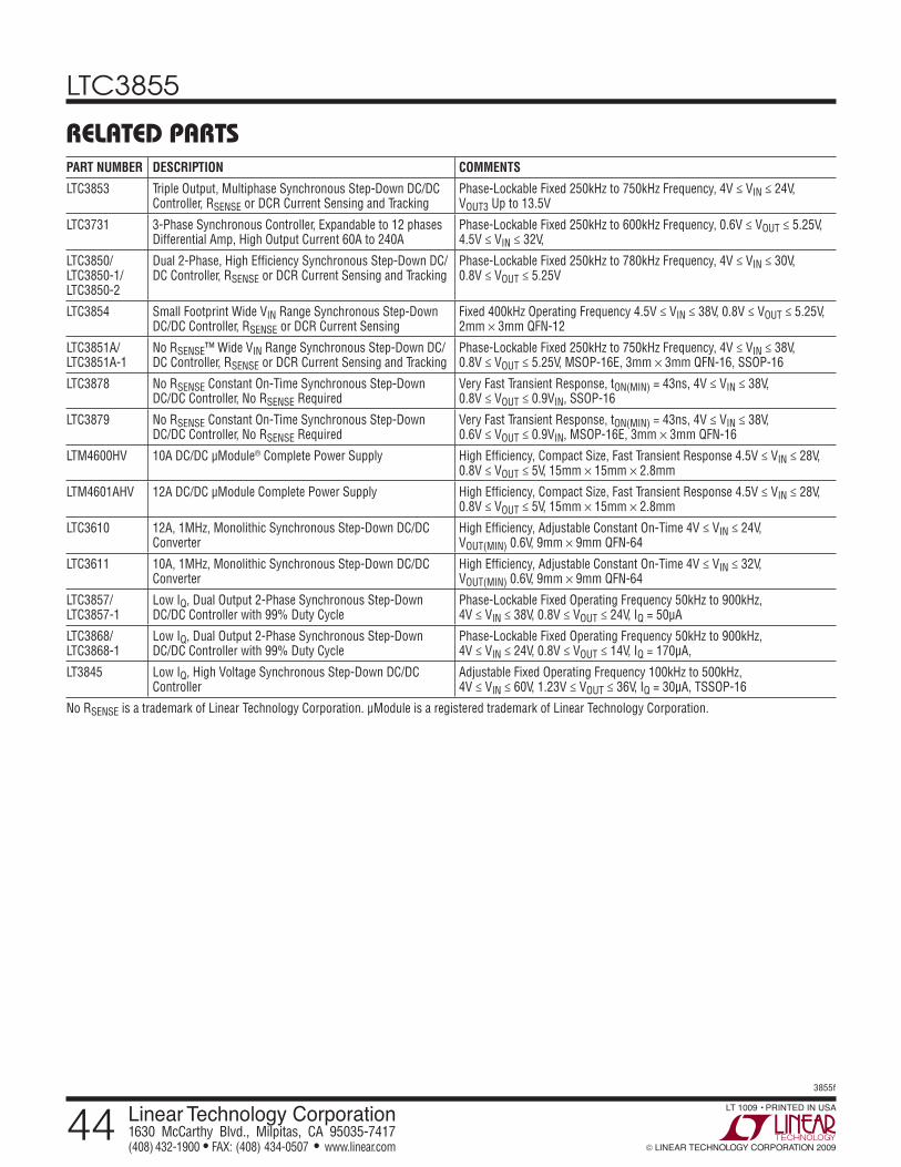
LTC3855
3855f
Linear Technology Corporation1630 McCarthy Blvd., Milpitas, CA 95035-7417 (408) 432-1900 FAX: (408) 434-0507 www.linear.com LINEAR TECHNOLOGY CORPORATION 2009
LT 1009 • PRINTED IN USA
relaTeD parTsPART NUMBER DESCRIPTION COMMENTS
LTC3853 Triple Output, Multiphase Synchronous Step-Down DC/DC Controller, RSENSE or DCR Current Sensing and Tracking
Phase-Lockable Fixed 250kHz to 750kHz Frequency, 4V ≤ VIN ≤ 24V, VOUT3 Up to 13.5V
LTC3731 3-Phase Synchronous Controller, Expandable to 12 phases Differential Amp, High Output Current 60A to 240A
Phase-Lockable Fixed 250kHz to 600kHz Frequency, 0.6V ≤ VOUT ≤ 5.25V, 4.5V ≤ VIN ≤ 32V,
LTC3850/LTC3850-1/LTC3850-2
Dual 2-Phase, High Efficiency Synchronous Step-Down DC/DC Controller, RSENSE or DCR Current Sensing and Tracking
Phase-Lockable Fixed 250kHz to 780kHz Frequency, 4V ≤ VIN ≤ 30V, 0.8V ≤ VOUT ≤ 5.25V
LTC3854 Small Footprint Wide VIN Range Synchronous Step-Down DC/DC Controller, RSENSE or DCR Current Sensing
Fixed 400kHz Operating Frequency 4.5V ≤ VIN ≤ 38V, 0.8V ≤ VOUT ≤ 5.25V, 2mm × 3mm QFN-12
LTC3851A/LTC3851A-1
No RSENSE™ Wide VIN Range Synchronous Step-Down DC/DC Controller, RSENSE or DCR Current Sensing and Tracking
Phase-Lockable Fixed 250kHz to 750kHz Frequency, 4V ≤ VIN ≤ 38V, 0.8V ≤ VOUT ≤ 5.25V, MSOP-16E, 3mm × 3mm QFN-16, SSOP-16
LTC3878 No RSENSE Constant On-Time Synchronous Step-Down DC/DC Controller, No RSENSE Required
Very Fast Transient Response, tON(MIN) = 43ns, 4V ≤ VIN ≤ 38V, 0.8V ≤ VOUT ≤ 0.9VIN, SSOP-16
LTC3879 No RSENSE Constant On-Time Synchronous Step-Down DC/DC Controller, No RSENSE Required
Very Fast Transient Response, tON(MIN) = 43ns, 4V ≤ VIN ≤ 38V, 0.6V ≤ VOUT ≤ 0.9VIN, MSOP-16E, 3mm × 3mm QFN-16
LTM4600HV 10A DC/DC µModule® Complete Power Supply High Efficiency, Compact Size, Fast Transient Response 4.5V ≤ VIN ≤ 28V, 0.8V ≤ VOUT ≤ 5V, 15mm × 15mm × 2.8mm
LTM4601AHV 12A DC/DC µModule Complete Power Supply High Efficiency, Compact Size, Fast Transient Response 4.5V ≤ VIN ≤ 28V, 0.8V ≤ VOUT ≤ 5V, 15mm × 15mm × 2.8mm
LTC3610 12A, 1MHz, Monolithic Synchronous Step-Down DC/DC Converter
High Efficiency, Adjustable Constant On-Time 4V ≤ VIN ≤ 24V, VOUT(MIN) 0.6V, 9mm × 9mm QFN-64
LTC3611 10A, 1MHz, Monolithic Synchronous Step-Down DC/DC Converter
High Efficiency, Adjustable Constant On-Time 4V ≤ VIN ≤ 32V, VOUT(MIN) 0.6V, 9mm × 9mm QFN-64
LTC3857/LTC3857-1
Low IQ, Dual Output 2-Phase Synchronous Step-Down DC/DC Controller with 99% Duty Cycle
Phase-Lockable Fixed Operating Frequency 50kHz to 900kHz, 4V ≤ VIN ≤ 38V, 0.8V ≤ VOUT ≤ 24V, IQ = 50µA
LTC3868/LTC3868-1
Low IQ, Dual Output 2-Phase Synchronous Step-Down DC/DC Controller with 99% Duty Cycle
Phase-Lockable Fixed Operating Frequency 50kHz to 900kHz, 4V ≤ VIN ≤ 24V, 0.8V ≤ VOUT ≤ 14V, IQ = 170µA,
LT3845 Low IQ, High Voltage Synchronous Step-Down DC/DC Controller
Adjustable Fixed Operating Frequency 100kHz to 500kHz, 4V ≤ VIN ≤ 60V, 1.23V ≤ VOUT ≤ 36V, IQ = 30µA, TSSOP-16
No RSENSE is a trademark of Linear Technology Corporation. µModule is a registered trademark of Linear Technology Corporation.
Related Documents