LOW POWER TECHNIQUES FOR ANALOG BUILDING BLOCKS OF THE ULTRA LOW POWER SYSTEM by Yen-Po Chen A dissertation submitted in partial fulfillment of the requirements for the degree of Doctor of Philosophy (Electrical Engineering) in the University of Michigan 2016 Doctoral Committee: Professor Dennis M. Sylvester, Chair Professor David Blaauw Assistant Professor Cynthia A. Chestek Associate Professor David D. Wentzloff

Welcome message from author
This document is posted to help you gain knowledge. Please leave a comment to let me know what you think about it! Share it to your friends and learn new things together.
Transcript
LOW POWER TECHNIQUES FOR
ANALOG BUILDING BLOCKS OF THE
ULTRA LOW POWER SYSTEM
by
Yen-Po Chen
A dissertation submitted in partial fulfillment
of the requirements for the degree of
Doctor of Philosophy
(Electrical Engineering)
in the University of Michigan
2016
Doctoral Committee:
Professor Dennis M. Sylvester, Chair
Professor David Blaauw
Assistant Professor Cynthia A. Chestek
Associate Professor David D. Wentzloff
ii
TABLE OF CONTENTS
LIST OF FIGURES.......................................................................................................................v
LIST OF TABLES........................................................................................................................xi
LIST OF APPENDICES.............................................................................................................xii
ABSTRACT……………............................................................................................................xiii
CHAPTER 1 Introduction ........................................................................................................... 1
1.1 The Requirement of Power Reduction of Analog Building Blocks ............................. 1
1.2 The Challenge of Power Reduction of Analog Building Blocks .................................. 3
1.3 Methods to Reduce the Power Consumption of the Analog Blocks ............................. 6
1.4 Contributions and Organization .................................................................................... 8
CHAPTER 2 Sample and Hold Bandgap Voltage Reference for Ultra Low Power System 13
2.1 Overview of Sample and Hold Bandgap Reference ................................................... 15
2.2 Technique to Decrease Duty-Cycle of Bandgap Reference ....................................... 16
2.3 Technique to Address Clock Injection Issue from Sample and Hold ......................... 21
2.4 Noise Analysis on Proposed Voltage Reference ........................................................ 21
2.5 Summary ..................................................................................................................... 26
CHAPTER 3 Low Power ESD Clamp Circuits for Ultra Low Power System...................... 28
3.1 Overview of Proposed Technique for ESD Protection Structure ............................... 30
iii
3.2 Proposed Technique for ESD Protection Structure under CMOS Technology .......... 32
3.3 Measurement Results .................................................................................................. 35
3.4 Summary ..................................................................................................................... 38
CHAPTER 4 Multiple-Choppers Technique to Increase the Noise Efficiency of the Low
Noise Amplifier............................................................................................................................ 39
4.1 Overview of the Fundamental Noise Limit of the Amplifier ..................................... 39
4.2 Proposed Multiple Chopper Scheme .......................................................................... 41
4.3 Implementation of Proposed Multiple Chopper Amplifier ......................................... 43
4.3 Implementation of the Bias of the Amplifier .............................................................. 47
4.4 Summary ..................................................................................................................... 47
CHAPTER 5 An Injectable 64nW ECG Mixed-Signal SoC in 65nm for Arrhythmia
Monitoring ................................................................................................................................... 50
5.1 Overview of the System .............................................................................................. 53
5.1.1 Dimension of the System ......................................................................................... 53
5.1.2 System Overview ..................................................................................................... 55
5.2 Implementation of the AFE ........................................................................................ 55
5.2.1 Noise Specification .................................................................................................. 56
5.2.2 Amplifier Implementation ....................................................................................... 58
5.2.3 ECG SAR ADC Overview....................................................................................... 63
5.2.4 Implementation of SAR Control Logic.................................................................... 64
iv
5.2.5 Implementation of DAC and Comparator................................................................ 66
5.3 Implementation of the Digital Back End .................................................................... 69
5.3.1 Overview of the Digital Algorithm .......................................................................... 69
5.3.2 Implementation of R-R Detection ............................................................................ 72
5.3.3 Implementation of the Frequency Dispersion Metric (FDM) .................................. 72
5.3.4 Optimization for Minimum Energy Computation ................................................... 73
5.4. Measurement Results ................................................................................................. 74
5.4.1 Proposed AFE Measured Results............................................................................. 74
5.4.2 Proposed SoC Measured Results ............................................................................. 76
5.4.3 Measurement Result with Peripherals ..................................................................... 78
5.5 Summary ..................................................................................................................... 81
CHAPTER 6 Conclusion ............................................................................................................ 83
6.1 Conclusion .................................................................................................................. 83
APPENDIX A Noise Analysis on Voltage Reference................................................................86
A.1 Noise analysis on bandgap voltage reference ............................................................ 83
A.2 Noise analysis on 2-T and 4-T voltage reference ...................................................... 92
APPENDIX B Pseudo Resistors Measured Results…………………………….…………….94
B.1 Introduction ................................................................................................................ 94
B.2 Measurement Results and Conclusions ...................................................................... 97
BIBLIOGRAPHY........................................................................................................................98

v
LIST OF FIGURES
Figure 1.1 The Bell’s Law of computer classes .............................................................................. 2
Figure 1.2 Scaling trend of the power supply voltage .................................................................... 4
Figure 1.3 Distribution of the ISSCC paper in 2005 [15] ............................................................... 5
Figure 1.4 Power breakdown example of a biomedical processor [94] .......................................... 5
Figure 1.5 Methods to reduce power consumption of analog building blocks ............................... 7
Figure 1.6 Basic concept of the sample and hold bandgap voltage reference ................................ 8
Figure 1.7 The concept of the multi-chopper amplifier .................................................................. 9
Figure 1.8 Power consumption breakdowns of [23] ..................................................................... 11
Figure 2.1The structure of the proposed sample and hold bandgap ............................................. 14
Figure 2.2 Low injection error switches and the structure of sample and hold block .................. 15
Figure 2.3 The primary leakage sources of the sample and hold circuits ..................................... 16
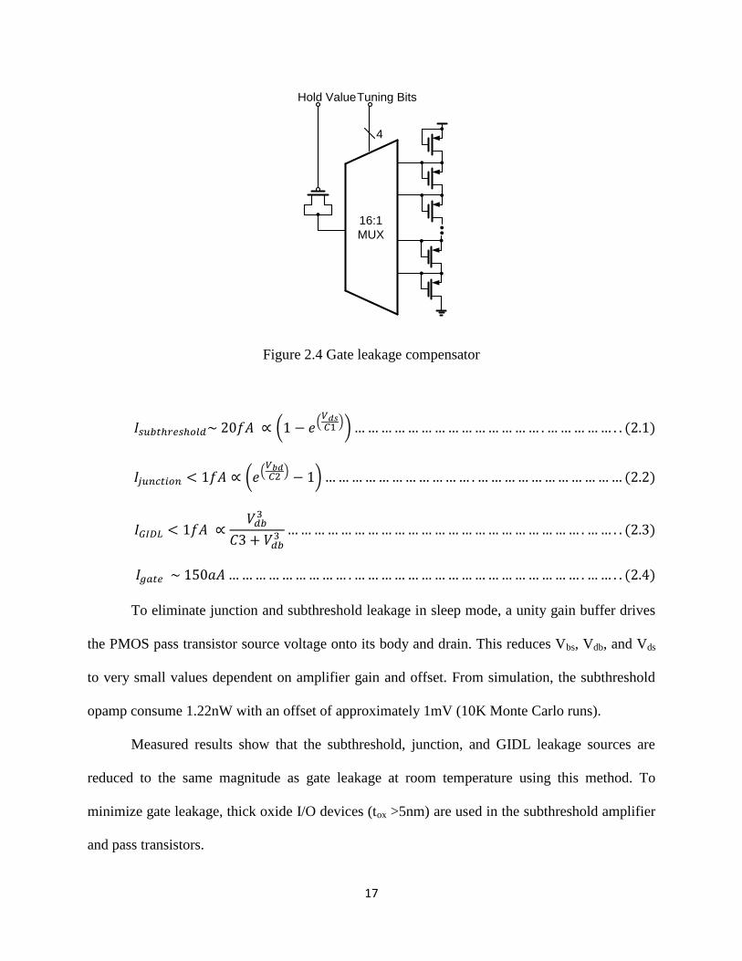
Figure 2.4 Gate leakage compensator ........................................................................................... 17
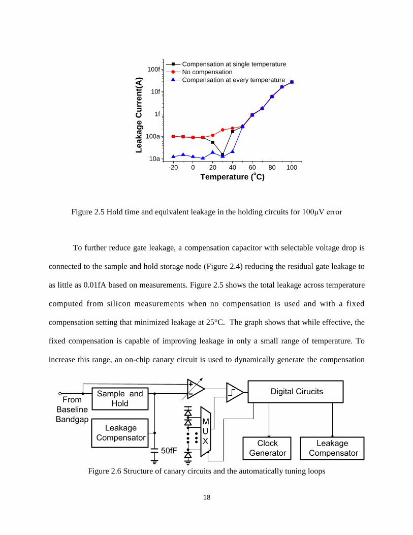
Figure 2.5 Hold time and equivalent leakage in the holding circuits for 100μV error ................. 18
Figure 2.6 Structure of canary circuits and the automatically tuning loops ................................. 18
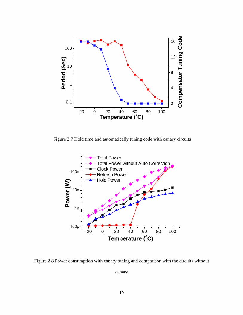
Figure 2.7 Hold time and automatically tuning code with canary circuits ................................... 19
Figure 2.8 Power consumption with canary tuning and comparison with the circuits without
canary .......................................................................................................................... 19
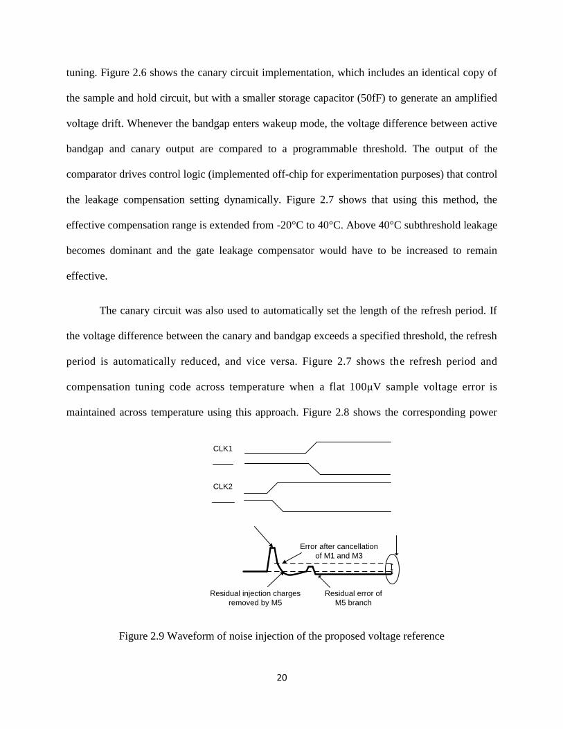
Figure 2.9 Waveform of noise injection of the proposed voltage reference ................................. 20
vi
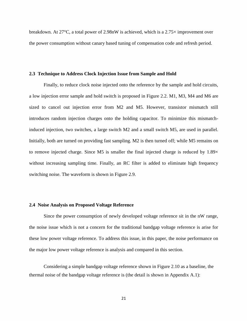
Figure 2.10 The baseline bandgap voltage reference .................................................................... 22
Figure 2.11: The 2 transistor and 4 transistor threshold voltage based voltage reference ............ 23
Figure 2.12 The calculated noise performance of the sample and hold bandgap voltage reference
..................................................................................................................................... 24
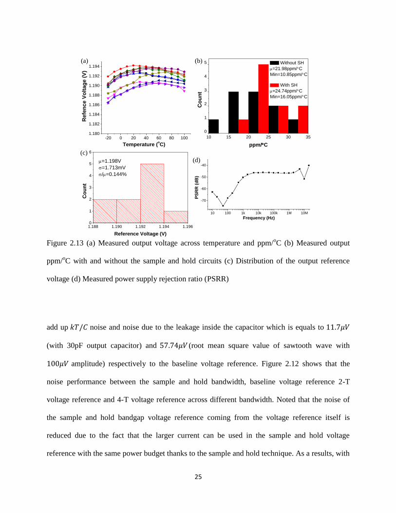
Figure 2.13 (a) Measured output voltage across temperature and ppm/oC (b) Measured output
ppm/oC with and without the sample and hold circuits (c) Distribution of the output
reference voltage (d) Measured power supply rejection ratio (PSRR) ....................... 25
Figure 2.14 Die photo of proposed reference ............................................................................... 26
Figure 3.1 Standard ESD schematic .............................................................................................. 28
Figure 3.2 Simulation waveform of the modified BJT based structure ......................................... 29
Figure 3.3 Power breakdown of standard ESD schematic ............................................................ 30
Figure 3.4 The modified BJT based structure ............................................................................... 30
Figure 3.5 Proposed GIDL reduction scheme ............................................................................... 31
Figure 3.6 GIDL reduction scheme for 3-stack (GIDL-1) with simulated internal node voltages
across temperature at 1.8V .......................................................................................... 32
Figure 3.7 Leakage-based GIDL reduction methods (GIDL-2) .................................................... 33
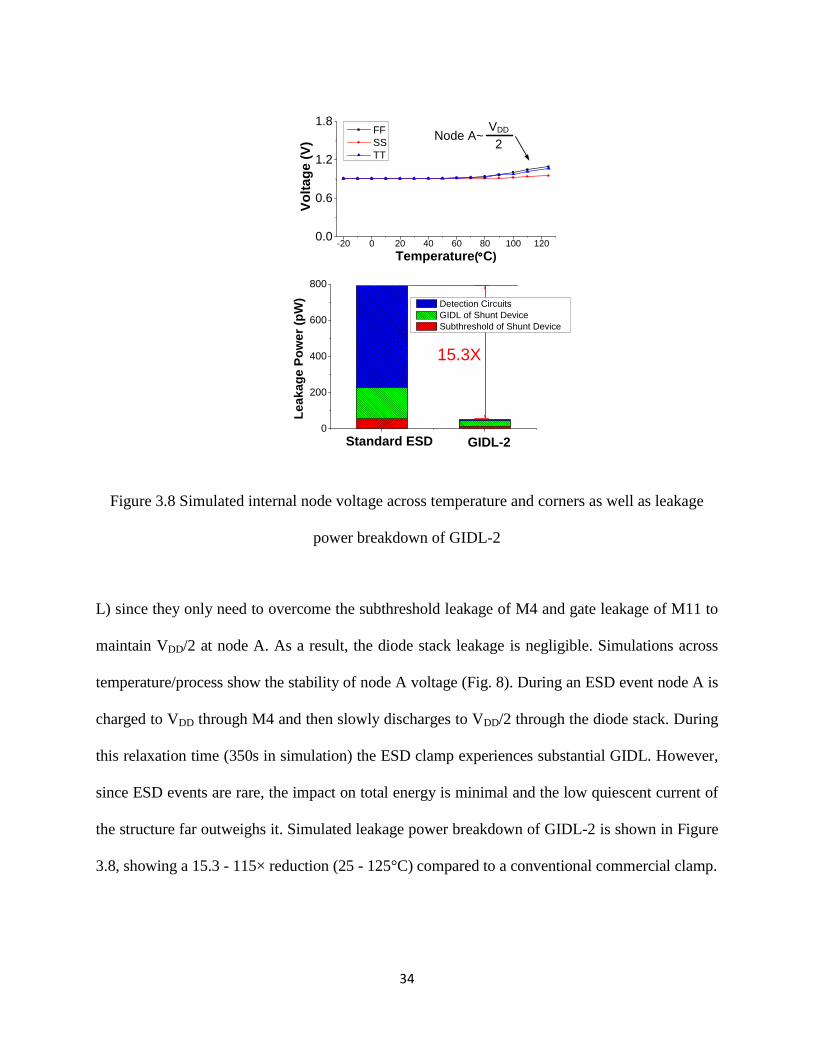
Figure 3.8 Simulated internal node voltage across temperature and corners as well as leakage
power breakdown of GIDL-2...................................................................................... 34
Figure 3.9 Testing setup with high voltage generator for human body model (HBM) and machine
model (MM) ................................................................................................................ 35
Figure 3.10 Measured leakage results across temperature and power supply ............................... 36
Figure 3.11 Measured scatter plot of baseline and 3 proposed structures ..................................... 36
Figure 3.12 Measured histogram of leakage for GIDL-2 across 20 measured dies ..................... 37
vii
Figure 4.1 Conceptual diagram of the multiple-chopper amplifier (2-stack version).................... 40
Figure 4.2 Signal and noise flow for each amplifier stage (2-stack version) ............................... 41
Figure 4.3 Schematic of stage 1 (left) and stage 2 (right) of the amplifier (2-stack version) ....... 43
Figure 4.4 Small signal analysis of the amplifier (2-stack version) .............................................. 44
Figure 4.5 Schematic of stage 3 and stage 4 of the amplifier (2-stack version) ........................... 45
Figure 4.6 Bias of the design (2-Stack Version) Noted that all resistor are made by pseudo
resistor ......................................................................................................................... 45
Figure 4.7 Measured gain across frequency range with 500Hz bandwidth ................................... 46
Figure 4.8 Measured noise across 1Hz - 1kHz .............................................................................. 48
Figure 4.9 Die photo in 180nm CMOS ......................................................................................... 49
Figure 5.1 (a) ECG waveform showing 60Hz interfering noise as recorded by proposed system.
(b) Sheep ECG waveform suffers from low frequency drift (measured by proposed
system). Note that the gain is reduced by 10× in this measurement ........................... 51
Figure 5.2 (a) Measured QRS peak amplitude versus electrode (use needles as the electrodes
directly) separation under the skin in a sheep experiment. Note that with >2cm
separation, the amplitude is larger than the traditional approach with two patches
attached to neck and wrist. (b) Dimensions of the proposed system .......................... 53
Figure 5.3 (a)Proposed nightly readout and recharge of the system. (b) Other required peripheral
..................................................................................................................................... 54
Figure 5.4 Top level diagram of the analog front end. .................................................................. 56
Figure 5.5 (a) The trade-off between amplifier current consumption and input referred noise
assumed constant (NEF). (b) The error rate across different noise levels with
sweeping threshold. In this plot the X-axis is true negative rate and the Y-axis is true
viii
positive rate. The line pass through (X,Y) = (0,1) shown in the 15μV case imply that
there is a threshold existed without any error in detection. Other line without passing
(X,Y) = (0,1) imply there is at least one false alarm when all the a-fib arrhythmia is
detected for any possible threshold ............................................................................. 57
Figure 5.6 The first stage of the low noise amplifier, including all building blocks: chopper, DC
servo loop, and impedance boosting loop ................................................................... 59
Figure 5.7 Core amplifier insides the CCIA .................................................................................. 60
Figure 5.8 Simulated CCIA gain versus frequency (without Gm-C filter)..................................... 61
Figure 5.9 (a) SAR ADC power breakdown with ADC logic implemented using HVT standard
cells. Note that SAR logic consumes 92% of total power when operating at 500Hz. (b)
SAR ADC power breakdown with custom asynchronous logic ................................. 63
Figure 5.10 Detailed signal flow diagram of the asynchronous controller inside the SAR ADC 64
Figure 5.11 Detailed diagram of asynchronus logic in the SAR ADC. Note that some of the reset
..................................................................................................................................... 64
Figure 5.12 (a) Traditional comparator and source of kickback noise. (b) The proposed
comparator with suppressed kickback noise sources .................................................. 67
Figure 5.13 Simulated waveforms of kickback noise in the proposed and traditional comparators.
Kickback noise in the traditional amplifier is 19.8mV and is reduced to 0.2mV in the
proposed design .......................................................................................................... 68
Figure 5.14 (a) Search windows of the proposed algorithm. (b) Example waveform of normal
ECG waveform and the arrhythmia ECG waveform (c) Corresponding power
spectrum of the ECG waveforms shown in (b). Noted that the block floating point
scheme is implemented and the y-axis is showing relative numbers without unit ..... 70
ix
Figure 5.15 (a) Top level of the proposed digital back end. (b) Energy/operation versus voltage
shows the minimum energy point of the FDM block ................................................. 71
Figure 5.16 Block diagram of FFT, peripheral buffers, and controller ........................................ 73
Figure 5.17 (a) Die photo of proposed SoC in 65nm LP CMOS. (b) Photo of proposed SOC and
a 14 gauge syringe needle. .......................................................................................... 75
Figure 5.18 The measure frequency response of the amplifier with the midband gain set to 59dB
..................................................................................................................................... 76
Figure 5.19 (a) Normal ECG waveform generated by ECG simulator and recorded by the
proposed system. (b) An arrhythmia waveform generated by ECG simulator
andrecorded and detected by the proposed system ..................................................... 78
Figure 5.20 (a) Test setup of the Human Chest Experiment. (b) The amplified waveform
observed from the amplifier output terminal by the Agilent oscilloscope. The Vol/Div
is 100mV/Div and the Time/Div is 0.5sec/Div ........................................................... 79
Figure 5.21 Test setup of complete system with simulator, proposed SoC, and [12] .................. 80
Figure 5.22 (a) The test setup of the sheep experiment. (b) The measure waveform of the
experiment. (c) The test setup of the isolated sheep heart experiment. (d) The
measure waveform of experiment from digital readout buffer. (downsampling by 10×)
..................................................................................................................................... 81
Figure A.1 The small signal model of the bandgap voltage reference ......................................... 86
Figure A.2 The small signal model of the 2-T and 4-T voltage reference .................................... 92
Figure B.1 Structure of a standard pseudo resistor ....................................................................... 94
Figure B.2 Measurement and simulation results of the pseudo resistor across different
temperature. Blue: FF(BSIM3), Green: FF(BSIM4), Red: TT(BSIM3), Orange:
x
TT(BSIM4), Brown: SS(BSIM3), Purple: SS(BSIM4) Others: 14 dies at the same run
..................................................................................................................................... 95

xi
LIST OF TABLES
Table 1.1 The theoretical performance scaling with the proposed N frequency multi-chopper
amplifier technique ..................................................................................................... 10
Table 2.1 Performance summaries and comparison to other previous works of voltage reference
..................................................................................................................................... 26
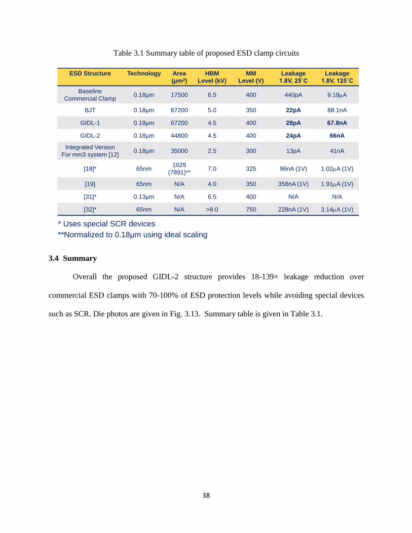
Table 3.1 Summary table of proposed ESD clamp circuits ........................................................... 38
Table 4.1 Summary table of the proposed amplifier and previous works .................................... 48
Table 5.1 Simulated specifications of the CCIA together with Gm-C filter .................................. 62
Table 5.2 Simulated power breakdown of analog front end .......................................................... 69
Table 5.3 Summary of measured results for SoC .......................................................................... 77
Table 5.4 Comparison table for the proposed ECG system .......................................................... 82
Table B.1 Measurement results across different voltage .............................................................. 96

xii
LIST OF APPENDICES
APPENDIX A Noise Analysis on Voltage Reference ............................................................... 86
A.1 Noise analysis on bandgap voltage reference ............................................................ 86
A.2 Noise analysis on 2-T and 4-T voltage reference ...................................................... 92
APPENDIX B Pseudo Resistors Measured Results ................................................................. 94
B.1 Introduction ................................................................................................................ 94
B.2 Measurement Results and Conclusions ...................................................................... 97
xiii
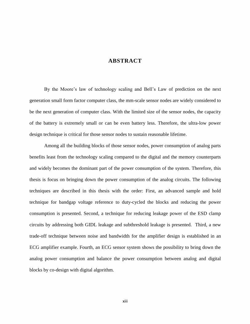
ABSTRACT
By the Moore’s law of technology scaling and Bell’s Law of prediction on the next
generation small form factor computer class, the mm-scale sensor nodes are widely considered to
be the next generation of computer class. With the limited size of the sensor nodes, the capacity
of the battery is extremely small or can be even battery less. Therefore, the ultra-low power
design technique is critical for those sensor nodes to sustain reasonable lifetime.
Among all the building blocks of those sensor nodes, power consumption of analog parts
benefits least from the technology scaling compared to the digital and the memory counterparts
and widely becomes the dominant part of the power consumption of the system. Therefore, this
thesis is focus on bringing down the power consumption of the analog circuits. The following
techniques are described in this thesis with the order: First, an advanced sample and hold
technique for bandgap voltage reference to duty-cycled the blocks and reducing the power
consumption is presented. Second, a technique for reducing leakage power of the ESD clamp
circuits by addressing both GIDL leakage and subthreshold leakage is presented. Third, a new
trade-off technique between noise and bandwidth for the amplifier design is established in an
ECG amplifier example. Fourth, an ECG sensor system shows the possibility to bring down the
analog power consumption and balance the power consumption between analog and digital
blocks by co-design with digital algorithm.

1
CHAPTER 1
Introduction
1.1 The Requirement of Power Reduction of Analog Building Blocks
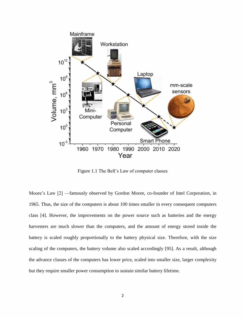
One of the most well-known quotes from the computer industry is the one formulated by
Gordon Bell in 1972. It is the Bell’s Law [1] of computer classes: “Roughly every decade, a new,
lower priced computer class forms based on a new programming platform, network, and
interface resulting in new usage and the establishing a new industry.” After roughly 40 years of
development of the computers industry, as shown in the Figure 1.1, we indeed have 4 computer
classes: From the workstations, personal computers, laptops to the portable smart phone devices.
The ongoing advances in both the process technology and the design technique enable the smart
sensors or IoT (Internet of things) devices to be considered the next generation of the computers
in the near future. Several prototype have been proposed and developed by both the academy and
the industry. For example, [90] demonstrated a system to monitor soil moisture, [91] proposed a
sensor to measure the pressure inside car tires, [92] developed a neural monitoring and
stimulation systems, [93] illustrated a MEMS sensor for gas detection.
Noted that the lower price of computer is mainly come from the smaller size and high
density of transistors thanks to the contributing from the technology scaling [3] predicted by the
2
Figure 1.1 The Bell’s Law of computer classes
Moore’s Law [2] —famously observed by Gordon Moore, co-founder of Intel Corporation, in
1965. Thus, the size of the computers is about 100 times smaller in every consequent computers
class [4]. However, the improvements on the power source such as batteries and the energy
harvesters are much slower than the computers, and the amount of energy stored inside the
battery is scaled roughly proportionally to the battery physical size. Therefore, with the size
scaling of the computers, the battery volume also scaled accordingly [95]. As a result, although
the advance classes of the computers has lower price, scaled into smaller size, larger complexity
but they require smaller power consumption to sustain similar battery lifetime.

3
Moreover, since these next generations sensing systems are most likely to be embedded
into location that is hard to access, shorter lifetime will lead to higher maintenance costs and
reduce the feasibility of such systems. For example, [55, 96] is implanted under human skins and
have a longer lifetime to reduce the recharge requirement is extremely important. To meet the
battery volume constraint and the lifetime requirement of such systems, low power consumption
technique on both the digital and analog blocks are a critical issue.
While the digital processor power scaled down with the prediction of the Gene’s Law [5],
the analog counterparts fall behind of the scaling. Moreover, if we foresee the next generation of
the computer, the mm-scale sensors [6-12], the power consumption budget can be as lower as
10nW [12]. Therefore, power reduction on the analog circuits is an active topic [13, 14]. And
following this trend, the topic on reducing the power consumption of the analog building blocks
will be the critical one for the next generation computer.
1.2 The Challenge of Power Reduction of Analog Building Blocks
People may wonder when the power consumption of the digital blocks scaled well with
the technology scaling [3], what is the reason behind the failure of the scaling of the analog block?
For the active power of the circuits, the power consumption of digital block can be
written as follows:
𝑃𝑜𝑤𝑒𝑟 ∝ 𝑉𝐷𝐷2 × 𝑓𝑐𝑙𝑘 × 𝐶𝑔𝑎𝑡𝑒 … … … … … … … … … … … … … … … … … … … … … … … (1.1)
We also know that:
𝐶𝑔𝑎𝑡𝑒 ∝ 𝑊𝑔 × 𝐿𝑔 ∝ 𝐿𝑔2 … … … … … … … … … … … … … … … … … … … … … … … … … … . (1.2)
Where 𝐿𝑔 is the channel length of the devices. The above equation (1.1-1.2) shows that
the active power consumption of the digital blocks are directly proportion to the area of the
4
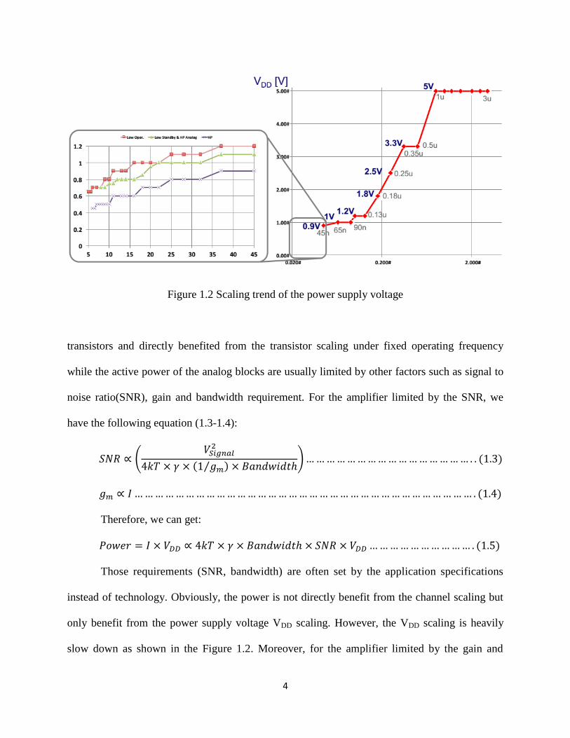
Figure 1.2 Scaling trend of the power supply voltage
transistors and directly benefited from the transistor scaling under fixed operating frequency
while the active power of the analog blocks are usually limited by other factors such as signal to
noise ratio(SNR), gain and bandwidth requirement. For the amplifier limited by the SNR, we
have the following equation (1.3-1.4):
𝑆𝑁𝑅 ∝ (𝑉𝑆𝑖𝑔𝑛𝑎𝑙
2
4𝑘𝑇 × 𝛾 × (1 𝑔𝑚⁄ ) × 𝐵𝑎𝑛𝑑𝑤𝑖𝑑𝑡ℎ) … … … … … … … … … … … … … … … … . . (1.3)
𝑔𝑚 ∝ 𝐼 … … … … … … … … … … … … … … … … … … … … … … … … … … … … … … … … … . (1.4)
Therefore, we can get:
𝑃𝑜𝑤𝑒𝑟 = 𝐼 × 𝑉𝐷𝐷 ∝ 4𝑘𝑇 × 𝛾 × 𝐵𝑎𝑛𝑑𝑤𝑖𝑑𝑡ℎ × 𝑆𝑁𝑅 × 𝑉𝐷𝐷 … … … … … … … … … … . (1.5)
Those requirements (SNR, bandwidth) are often set by the application specifications
instead of technology. Obviously, the power is not directly benefit from the channel scaling but
only benefit from the power supply voltage VDD scaling. However, the VDD scaling is heavily
slow down as shown in the Figure 1.2. Moreover, for the amplifier limited by the gain and
5
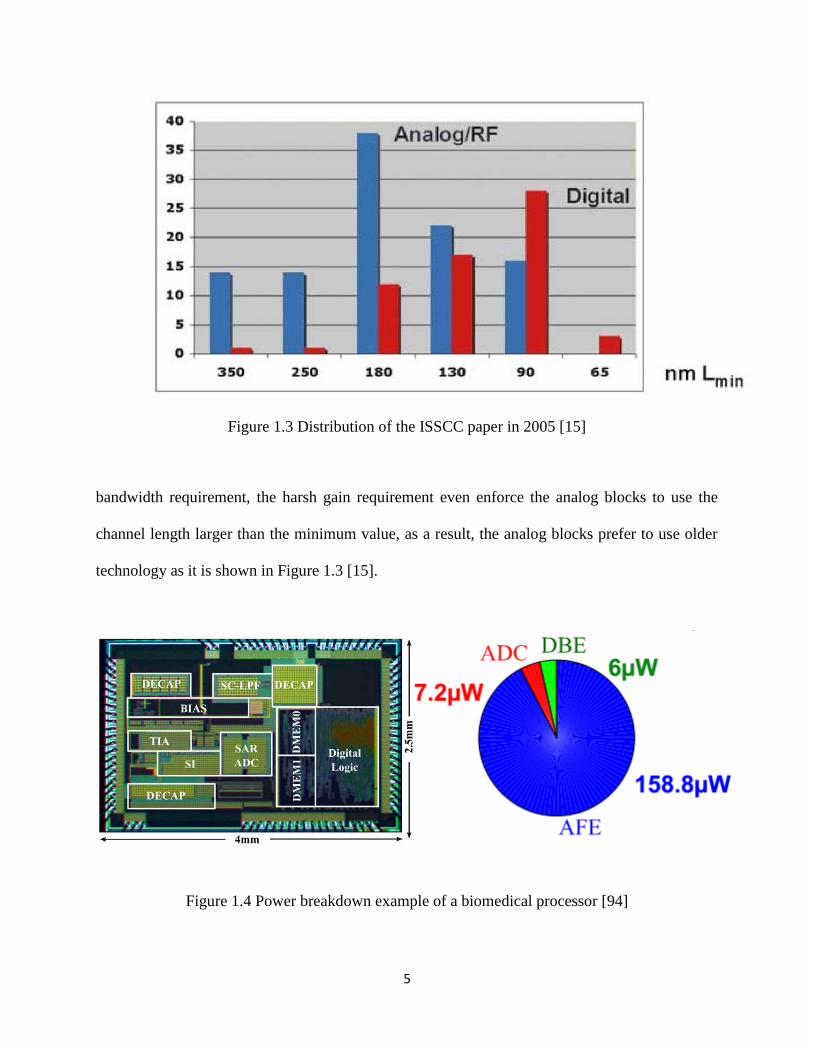
Figure 1.3 Distribution of the ISSCC paper in 2005 [15]
bandwidth requirement, the harsh gain requirement even enforce the analog blocks to use the
channel length larger than the minimum value, as a result, the analog blocks prefer to use older
technology as it is shown in Figure 1.3 [15].
Figure 1.4 Power breakdown example of a biomedical processor [94]

6
For the leakage power of the circuits, while the digital blocks utilize the smallest possible
channel width of each technology, the analog blocks require to use larger channel width for
reducing flicker noise, maintain in the saturation region and conduct large active current.
Therefore, the analog blocks usually have larger leakage current than the digital blocks. Also,
while the digital blocks usually power gated and consume only leakage power. The analog
blocks such as sensor interface, wakeup receiver and voltage reference are required to be always
on and consume active power instead of sleep power [11-14]. As a result, the power
consumption of the entire IoT system are usually dominate by the analog blocks. Figure 1.4
shows an example of the power breakdown of such a system.
In conclusion, the analog blocks power scaled little compared to the digital block, and the
development on the technique to reduce the power consumption is vital for the next generation
computers.
1.3 Methods to Reduce the Power Consumption of the Analog Blocks
To address of the power consumption problems of the analog building blocks as
mentioned in the section 1.2. This thesis is targeting on reducing the power consumption of the
analog blocks. As it is shown in the Figure 1.5(a), for the ultra-low power system, the power
consumption of the analog builds blocks usually consist of two parts: the leakage power and the
active power (Equation 1.6).
𝑇𝑜𝑡𝑎𝑙 𝑃𝑜𝑤𝑒𝑟 = 𝐴𝑐𝑡𝑖𝑣𝑒 𝑅𝑎𝑡𝑒 × 𝐴𝑐𝑡𝑖𝑣𝑒 𝑃𝑜𝑤𝑒𝑟 + 𝑆𝑙𝑒𝑒𝑝 𝑃𝑜𝑤𝑒𝑟 … … … … … … … … (1.6)
As it is shown in the Figure 1.5(b), in chapter 2, the main focus will be on reducing the
duty cycle of a bandgap voltage reference which is an essential building block for the system. In
chapter 3, it is focus on reduce the leakage power of the ESD pad, which is the dominant leakage
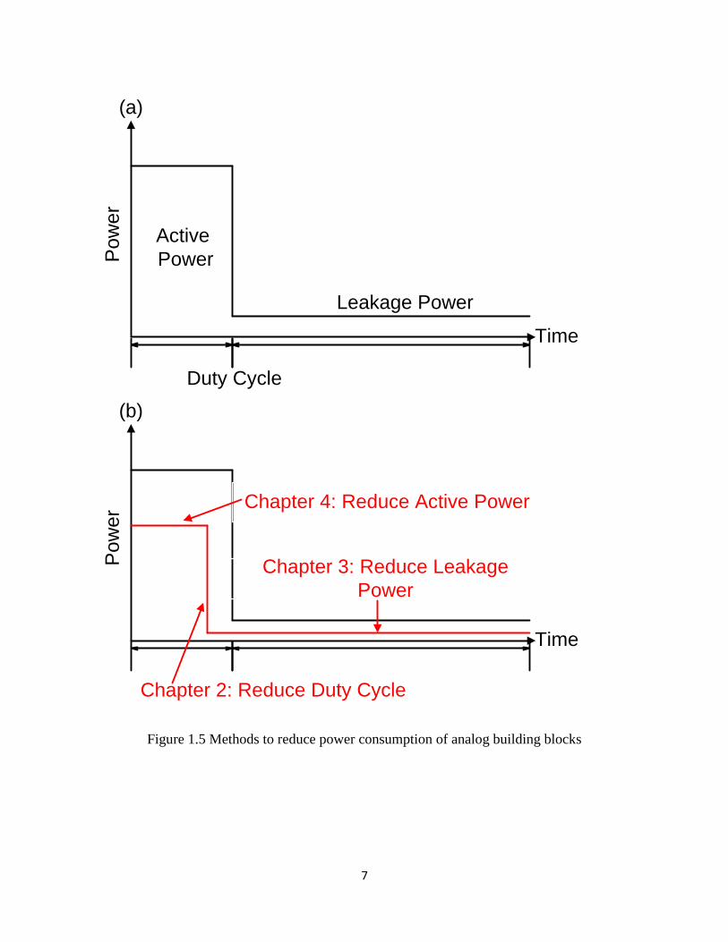
7
Leakage Power
Active
PowerPo
we
r
Time
Duty Cycle
(a)
Chapter 4: Reduce Active Power
Po
we
r
Time
Chapter 2: Reduce Duty Cycle
(b)
Chapter 3: Reduce Leakage
Power
Figure 1.5 Methods to reduce power consumption of analog building blocks
8
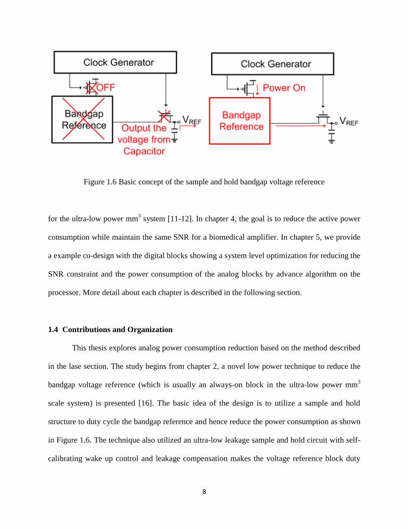
Figure 1.6 Basic concept of the sample and hold bandgap voltage reference
for the ultra-low power mm3 system [11-12]. In chapter 4, the goal is to reduce the active power
consumption while maintain the same SNR for a biomedical amplifier. In chapter 5, we provide
a example co-design with the digital blocks showing a system level optimization for reducing the
SNR constraint and the power consumption of the analog blocks by advance algorithm on the
processor. More detail about each chapter is described in the following section.
1.4 Contributions and Organization
This thesis explores analog power consumption reduction based on the method described
in the lase section. The study begins from chapter 2, a novel low power technique to reduce the
bandgap voltage reference (which is usually an always-on block in the ultra-low power mm3
scale system) is presented [16]. The basic idea of the design is to utilize a sample and hold
structure to duty cycle the bandgap reference and hence reduce the power consumption as shown
in Figure 1.6. The technique also utilized an ultra-low leakage sample and hold circuit with self-
calibrating wake up control and leakage compensation makes the voltage reference block duty
9
Figure 1.7 The concept of the multi-chopper amplifier
cycled with extremely low active rate. The proposed circuits is implemented in 180nm CMOS,
and it shows a temperature coefficient of 24.7ppm/°C and power consumption of 2.98nW which
marks a 251× power improvement over the best prior bandgap voltage reference.
In chapter 3, an ultralow-leakage electrostatic discharge (ESD) power clamp designs for
wireless sensor applications are proposed and implemented in 0.18μm CMOS is presented [17].
The ESD Structure is required to be always active to have minimum response time to discharge
the electrostatic events. Also, due to the nature of the ESD clamp needs to have relative larger
width for conducting massive electrostatic current, the ESD clamp experience almost largest
leakage among all the blocks. The power consumption of typical ESD pads are at nano watt
range and the total power consumption from all the pads are easily excess the 10nW budget of
the ultra-low power system. While a typical ESD power clamp structure consume at nano watt
f1
f2
f1
f2
Multiple Input
Multiple Output
Amplifier
Signal In
n1(t)
n2(t)
f3n3(t)f3
10
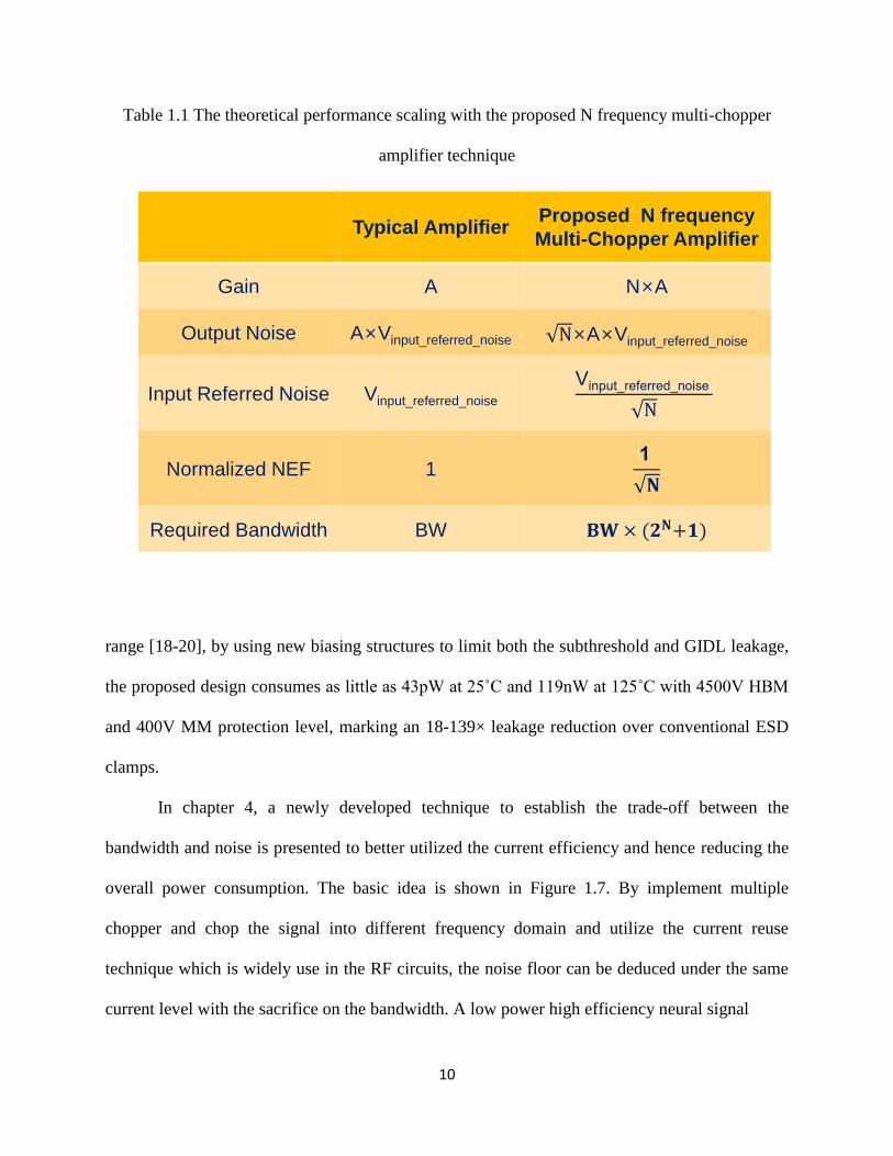
Table 1.1 The theoretical performance scaling with the proposed N frequency multi-chopper
amplifier technique
range [18-20], by using new biasing structures to limit both the subthreshold and GIDL leakage,
the proposed design consumes as little as 43pW at 25˚C and 119nW at 125˚C with 4500V HBM
and 400V MM protection level, marking an 18-139× leakage reduction over conventional ESD
clamps.
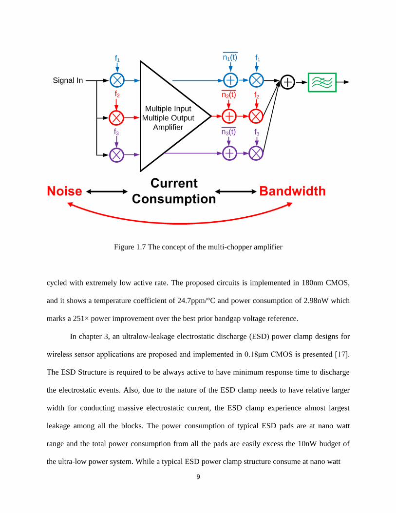
In chapter 4, a newly developed technique to establish the trade-off between the
bandwidth and noise is presented to better utilized the current efficiency and hence reducing the
overall power consumption. The basic idea is shown in Figure 1.7. By implement multiple
chopper and chop the signal into different frequency domain and utilize the current reuse
technique which is widely use in the RF circuits, the noise floor can be deduced under the same
current level with the sacrifice on the bandwidth. A low power high efficiency neural signal
Typical AmplifierProposed N frequency
Multi-Chopper Amplifier
Gain A N×A
Output Noise A×Vinput_referred_noise ×A×Vinput_referred_noise
Input Referred Noise Vinput_referred_noise
Normalized NEF 1
Required Bandwidth BW
11
7%
21.81%11.11%
16.46%
43.62%
Analog Front End
Bandgap Reference
Oscillator
ADC
Others
Dominant!
Figure 1.8 Power consumption breakdowns of [23]
recording amplifier with the above novel multi-chopper technique is proposed and implemented
in 180nm CMOS to demonstrate this technique [21]. The input referred root mean square noise is
1.54μV (1-500Hz) with 266nA tail current. The result corresponds to a 1.38 noise efficiency
factor, which is the best reported among current state-of-the-art amplifiers and is lower than the
theoretical limit of the differential amplifier (NEF = √2). Table 1.1 shows the summarized
results of this technique.
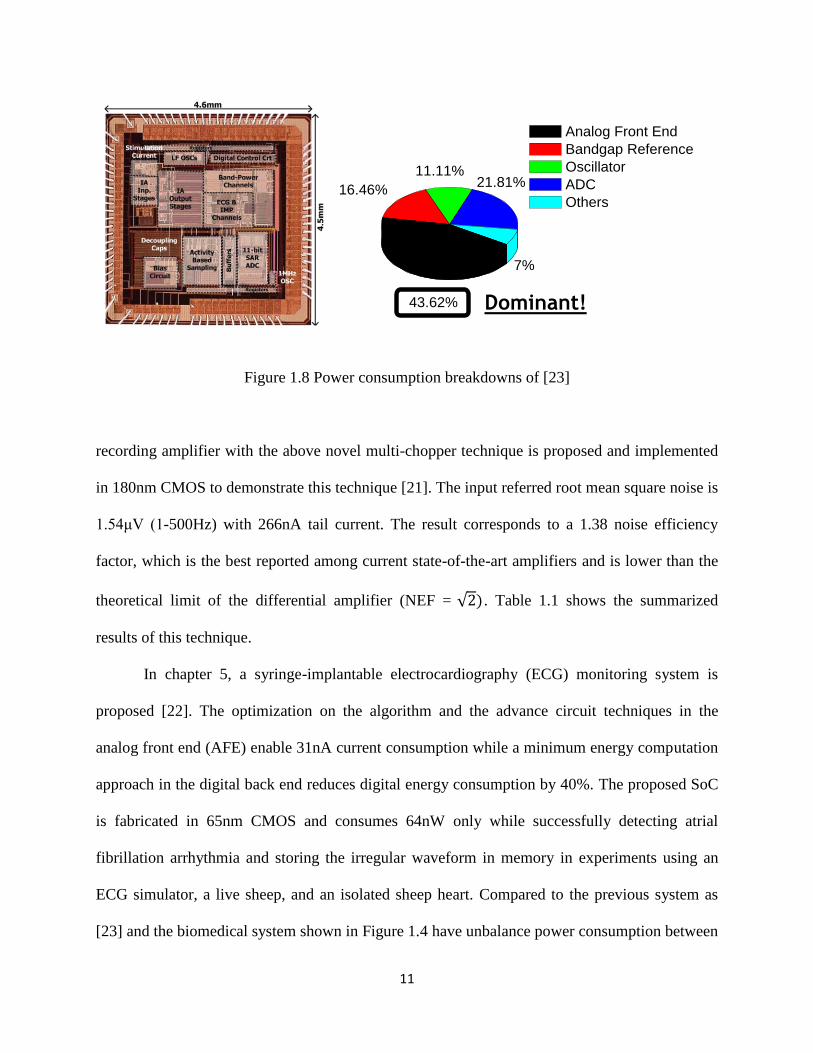
In chapter 5, a syringe-implantable electrocardiography (ECG) monitoring system is
proposed [22]. The optimization on the algorithm and the advance circuit techniques in the
analog front end (AFE) enable 31nA current consumption while a minimum energy computation
approach in the digital back end reduces digital energy consumption by 40%. The proposed SoC
is fabricated in 65nm CMOS and consumes 64nW only while successfully detecting atrial
fibrillation arrhythmia and storing the irregular waveform in memory in experiments using an
ECG simulator, a live sheep, and an isolated sheep heart. Compared to the previous system as
[23] and the biomedical system shown in Figure 1.4 have unbalance power consumption between

12
analog and digital blocks as shown in Figure 1.8 the analog front end power and digital power
are well balanced thanks to the co-optimize on the system level.
Several techniques are developed in this thesis and offered new insights on the low power
analog circuits design. All the presented projects and possible future works are concluded in
chapter 6.
To summarize, this work makes the following new contributions:
Develop a technique to reduce the duty cycle of the bandgap voltage reference.
Demonstrate a technique to reduce the leakage power of the ESD pads which is the
dominant leakage source in many low power systems.
Discuss the theoretical limit of the power consumption of the amplifier due to the noise
requirement and develop a technique to push the limit with the cost of the bandwidth
Present a whole ECG system design to show how to balance and optimize the power
consumption between the analog and digital block
13
CHAPTER 2
Sample and Hold Bandgap Voltage Reference for
Ultra Low Power System
A precision voltage reference that is insensitive to process, voltage, and temperature
fluctuations is a key building block in mixed-signal and analog systems. Given a recent emphasis
on low-power battery-operated systems, including wireless sensors, ultra-low power voltage
references are needed. Many low power voltage reference circuits have been presented [24]-[28].
In [24, 25], different Vth devices are used to achieve low power consumption while the output
voltage of the design in [26] is equal to Vth. However, Vth can vary substantially (particularly
across device flavors), and is highly technology dependent. The voltage of Bandgap references
are set by fundamental parameters and therefore exhibit lower process spread. However, their
power consumption is higher; a prior work on low power bandgap reference presented in [27]
consumes 1μW, which is large relative to recent ultra-low power microsystems [12] with nW
power budgets. New structures for bandgap references have been developed [28], but power
remains in the μW range. Some duty cycled bandgap reference is presented [29-30]. However
the large noise [29] and specialized fabrication requirements [30] of these works are design goal
to avoid in this work.
14
Bandgap Reference
SH
SH
SH
SH
Sample and Hold
Output Filter
Clocking Unit
C1
C2
C3
C4
C5
R1
C1 = C2 = C3 = C4 = 2pFC5 = 30pFR2 = R3 = 6.5R1 = 6.5MΩ
Non-overlapping
Clock Generator
CLK0
CLK2
CLK1
CLK2
CLK0
CLK1
Leakage
Compensator
Leakage -Based
Oscillator
Canary Circuits
Canary Circuits
VREF
R3 R2
R1
Figure 2.1The structure of the proposed sample and hold bandgap
In this chapter, we present a low power reference that consumes 2.98nW at room
temperature in 180nm CMOS. The reference uses a sample and hold technique where the
bandgap is duty-cycled to save power consumption. A low (0.015 at 25°C) duty cycle is
achieved through three methods: 1) Sampling, holding and restoring the internal node voltages of
the bandgap reduces the refresh time by 11.5×; 2) Equalizing the voltage across the sample and
hold switch using a subthreshold opamp, increases the sleep time by three orders of magnitude; 3)
15
Sample
Node
Hold Node
M1
M2
M3
M4
M5
M6
CLK2
CLK2
CLK1
CLK1
CLK
CLK
To Holding
Capacitor C1-C4From
Bandgap
Connect to
NWELL
Feedback
Node
M2=2μm
M1=M3=1μm
M5=700nm
M4=M6=350nm
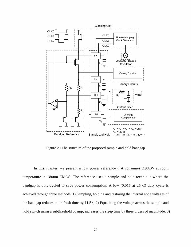
Figure 2.2 Low injection error switches and the structure of sample and hold block
Automatic tuning of sleep time and a gate leakage compensation capacitor using a canary circuit
maintains optimal power consumption across temperature. Finally, a new low injection error
switch structure reduces noise from the sample and hold circuits. Each of these methods will be
explained in more detail below.
2.1 Overview of Sample and Hold Bandgap Reference
Figure 2.1 shows the structure of the proposed sample and hold bandgap. The bandgap
itself is a traditional design with single point trimming of the resistor. In active mode, the
bandgap is ON (CLK0 is low) and the output and intermediate node voltages are stored on
sample and hold capacitors C1–C5. In sleep mode CLK0 goes high to power gate the bandgap,
while the sample and hold circuits continue to output the reference voltage. A delay line
generates clocks for the sample and hold switches and bandgap power gate using an on-chip
leakage-based oscillator, periodically waking the bandgap and refreshing the voltage levels.
16
2.2 Technique to Decrease Duty-Cycle of Bandgap Reference
Power consumption during the active and sleep modes is dramatically different (aft),
making average power heavily dependent on achievable bandgap duty cycle. The two critical
factors determining duty cycle are bandgap wake-up time and leakage in the sample and hold
circuits. To speed bandgap wakeup and stabilization time, three internal nodes are sampled in
addition to the reference output voltage using capacitors C1- C4 (Figure 2.1). Once the bandgap
enters wake-up mode, these stored values drive the nodes inside the bandgap, speeding wake-up
by 11.5× (from 55ms to 4.8ms) based on simulation.
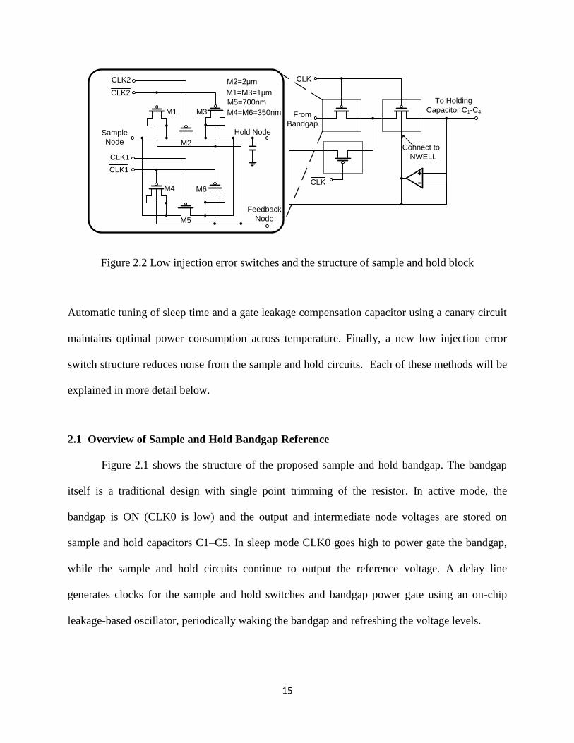
To reduce leakage in the sample and hold circuits, a feedback structure is used as shown
in Figure 2.2. The main sources of leakage in the sample and hold circuit are shown in Figure 2.3.
And the following equation shows the leakage for each source and its formula (2.1)-(2.4):
P-sub
N-WellIsub, IGIDL
IGate
Ijunction
B D S
G
IGate
SampleSample
Sample Value
Hold ValueSample
Leakage PathDriving Path
Figure 2.3 The primary leakage sources of the sample and hold circuits
17
Hold Value
16:1
MUX
Tuning Bits
4
Figure 2.4 Gate leakage compensator
𝐼𝑠𝑢𝑏𝑡ℎ𝑟𝑒𝑠ℎ𝑜𝑙𝑑~ 20𝑓𝐴 ∝ (1 − 𝑒(𝑉𝑑𝑠𝐶1
)) … … … … … … … … … … … … … … . … … … … … . . (2.1)
𝐼𝑗𝑢𝑛𝑐𝑡𝑖𝑜𝑛 < 1𝑓𝐴 ∝ (𝑒(𝑉𝑏𝑑𝐶2
) − 1) … … … … … … … … … … … . … … … … … … … … … … … (2.2)
𝐼𝐺𝐼𝐷𝐿 < 1𝑓𝐴 ∝𝑉𝑑𝑏
3
𝐶3 + 𝑉𝑑𝑏3 … … … … … … … … … … … … … … … … … … … … … … . … … . . (2.3)
𝐼𝑔𝑎𝑡𝑒 ~ 150𝑎𝐴 … … … … … … … … … . … … … … … … … … … … … … … … … … … . … … . . (2.4)
To eliminate junction and subthreshold leakage in sleep mode, a unity gain buffer drives
the PMOS pass transistor source voltage onto its body and drain. This reduces Vbs, Vdb, and Vds
to very small values dependent on amplifier gain and offset. From simulation, the subthreshold
opamp consume 1.22nW with an offset of approximately 1mV (10K Monte Carlo runs).
Measured results show that the subthreshold, junction, and GIDL leakage sources are
reduced to the same magnitude as gate leakage at room temperature using this method. To
minimize gate leakage, thick oxide I/O devices (tox >5nm) are used in the subthreshold amplifier
and pass transistors.
18
-20 0 20 40 60 80 100
10a
100a
1f
10f
100f
Le
ak
ag
e C
urr
en
t(A
)
Temperature (oC)
Compensation at single temperature
No compensation
Compensation at every temperature
Figure 2.5 Hold time and equivalent leakage in the holding circuits for 100μV error
To further reduce gate leakage, a compensation capacitor with selectable voltage drop is
connected to the sample and hold storage node (Figure 2.4) reducing the residual gate leakage to
as little as 0.01fA based on measurements. Figure 2.5 shows the total leakage across temperature
computed from silicon measurements when no compensation is used and with a fixed
compensation setting that minimized leakage at 25°C. The graph shows that while effective, the
fixed compensation is capable of improving leakage in only a small range of temperature. To
increase this range, an on-chip canary circuit is used to dynamically generate the compensation
Leakage
Compensator
From
Baseline
Bandgap M
U
X50fF
Digital Cirucits
Clock
Generator
Leakage
Compensator
Sample and
Hold
Figure 2.6 Structure of canary circuits and the automatically tuning loops
19
-20 0 20 40 60 80 100
0.1
1
10
100
Temperature (oC)
Pe
rio
d (
Se
c)
0
4
8
12
16
Co
mp
en
sa
tor
Tu
nin
g C
od
e
Figure 2.7 Hold time and automatically tuning code with canary circuits
-20 0 20 40 60 80 100100p
1n
10n
100n
Total Power
Total Power without Auto Correction
Clock Power
Refresh Power
Hold Power
Po
wer
(W)
Temperature (oC)
Figure 2.8 Power consumption with canary tuning and comparison with the circuits without
canary
20
tuning. Figure 2.6 shows the canary circuit implementation, which includes an identical copy of
the sample and hold circuit, but with a smaller storage capacitor (50fF) to generate an amplified
voltage drift. Whenever the bandgap enters wakeup mode, the voltage difference between active
bandgap and canary output are compared to a programmable threshold. The output of the
comparator drives control logic (implemented off-chip for experimentation purposes) that control
the leakage compensation setting dynamically. Figure 2.7 shows that using this method, the
effective compensation range is extended from -20°C to 40°C. Above 40°C subthreshold leakage
becomes dominant and the gate leakage compensator would have to be increased to remain
effective.
The canary circuit was also used to automatically set the length of the refresh period. If
the voltage difference between the canary and bandgap exceeds a specified threshold, the refresh
period is automatically reduced, and vice versa. Figure 2.7 shows the refresh period and
compensation tuning code across temperature when a flat 100μV sample voltage error is
maintained across temperature using this approach. Figure 2.8 shows the corresponding power
CLK2
CLK1
Residual error of
M5 branch
Error after cancellation
of M1 and M3
Residual injection charges
removed by M5
Figure 2.9 Waveform of noise injection of the proposed voltage reference
21
breakdown. At 27°C, a total power of 2.98nW is achieved, which is a 2.75× improvement over
the power consumption without canary based tuning of compensation code and refresh period.
2.3 Technique to Address Clock Injection Issue from Sample and Hold
Finally, to reduce clock noise injected onto the reference by the sample and hold circuits,
a low injection error sample and hold switch is proposed in Figure 2.2. M1, M3, M4 and M6 are
sized to cancel out injection error from M2 and M5. However, transistor mismatch still
introduces random injection charges onto the holding capacitor. To minimize this mismatch-
induced injection, two switches, a large switch M2 and a small switch M5, are used in parallel.
Initially, both are turned on providing fast sampling. M2 is then turned off; while M5 remains on
to remove injected charge. Since M5 is smaller the final injected charge is reduced by 1.89×
without increasing sampling time. Finally, an RC filter is added to eliminate high frequency
switching noise. The waveform is shown in Figure 2.9.
2.4 Noise Analysis on Proposed Voltage Reference
Since the power consumption of newly developed voltage reference sit in the nW range,
the noise issue which is not a concern for the traditional bandgap voltage reference is arise for
these low power voltage reference. To address this issue, in this paper, the noise performance on
the major low power voltage reference is analysis and compared in this section.
Considering a simple bandgap voltage reference shown in Figure 2.10 as a baseline, the
thermal noise of the bandgap voltage reference is (the detail is shown in Appendix A.1):
22
R2 R3=R2
R1
Q1 Q2= N☓Q1
M3
A
Figure 2.10 The baseline bandgap voltage reference
Vn,total2
=
((4kTR1 +2qIgm1
2 ) (gm3
gm1A − 1)
2
+ 4kTR2 ((gm3A(R1 +1
gm1) + 1)
2
) (gm1R2 + 1)2
(gm1gm3AR1R2 + (2gm1R2 + gm1R1 + 2))2
+
(4kTR2 (gm3
gm1A − 1)
2
+2qIgm1
2 (gm3AR2 + 1)2) (gm1R2 + gm1R1 + 1)2
(gm1gm3AR1R2 + (2gm1R2 + gm1R1 + 2))2
+
(Vn2 gm3
2
gm12 A2 + 4kTγ
gm3
gm12 )(gm1R2 + 1)2(gm1R2 + gm1R1 + 1)2
(gm1gm3AR1R2 + (2gm1R2 + gm1R1 + 2))2
… … … … … … … … … . . … (2.5)
Noted that I is the current in either BJT branch, A is the gain of the amplifier and the
amplifier noise is 𝑉𝑛. Also since 𝑅2 is equals to 𝑅3, the current at the two branch are equals.
Therefore, 𝑔𝑚1 =𝐼𝑄1
𝑉𝑡=
𝐼𝑄2
𝑉𝑡= 𝑔𝑚2 and there is no 𝑅3 and 𝑔𝑚2 in the equation. By considering
every gmR term is larger than 1 and the amplifier gain is also much larger than 1, we can
simplify the equation to be:
23
Vref
Vref
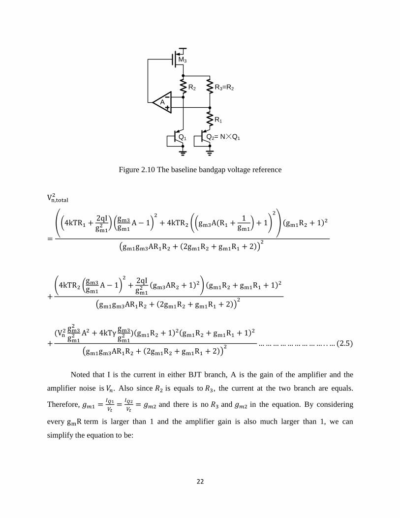
(a) 2-T voltage reference (b) 4-T voltage reference
M1
M2
M1
M2
M3
M4
Figure 2.11: The 2 transistor and 4 transistor threshold voltage based voltage reference
Vn,total2 ≅ 4𝑘𝑇𝑅2 +
2𝑞𝐼
𝑔𝑚12 (1 + (
R2 + R1
R1 )
2
) + (R2 + R1
R1 )
2
Vn2 … … … … … … … … … … … . . (2.6)
In this design, the current of the amplifier is set to be equal to the sum of the two branches
of the bandgap voltage reference to balance the noise contribution, and the design point is
𝑉𝑜𝑣,𝑎𝑚𝑝𝑙𝑖𝑓𝑖𝑒𝑟 = 0.1 , 𝑉𝑜𝑢𝑡 = 1.2 and 𝑉𝐵𝐸1 = 0.6. Therefore, 𝐼 = 𝐼𝑡𝑜𝑡𝑎𝑙/4 , 𝑉𝑛2 = 4 × 4𝑘𝑇𝛾
1
𝑔𝑚=
6.4𝑘𝑇/3𝐼𝑡𝑜𝑡𝑎𝑙 , 𝑅2 = 2.4/𝐼𝑡𝑜𝑡𝑎𝑙 , 𝑅2 = 6.5𝑅1 and 2𝑞𝐼/𝑔𝑚12 = 8𝑞𝑉𝑡
2/𝐼𝑡𝑜𝑡𝑎𝑙 . And the equation
becomes:
𝑉𝑛,𝑡𝑜𝑡𝑎𝑙2 ≅
9.6𝑘𝑇
𝐼𝑡𝑜𝑡𝑎𝑙+
86.5𝑞𝑉𝑡2
𝐼𝑡𝑜𝑡𝑎𝑙+
270.4𝑘𝑇
3𝐼𝑡𝑜𝑡𝑎𝑙… … … … … … … … … … … … … … … … … … … … … … … . . (2.7)
To also compare with other threshold voltage (Figure 2.11) based voltage reference, the
noise performance of such reference is also being analysis in Appendix A.2. The following
equation shows the noise performance of 2-T and 4-T based voltage reference:
𝑉𝑛𝑜𝑖𝑠𝑒,2𝑇2 ≅
𝑞𝑛2𝑉𝑡2
𝐼… … … … … … … … … … … … … … … … … … … … … … … … … … … … … … … … … . . (2.8)
24
𝑉𝑛𝑜𝑖𝑠𝑒,4𝑇2 ≅
2𝑞𝑛2𝑉𝑡2
𝐼2… … … … … … … … … . … … … … … … … … … … … … … … … … … … … … … … … . . (2.9)
Note that the current I2 is the current pass through transistor M3 and M4, which is typically at
least 10x smaller than the total current. The equation shows that the noise current relationship of
the voltage reference is similar to the amplifier and the normal bandgap voltage reference with
different scaling constant.
For a voltage reference consume 2.98nW at 1.8V VDD, the baseline bandgap voltage
reference has noise 𝑉𝑛 around 15.9𝜇𝑉/√𝐻𝑧 while the 2-T and 4-T voltage reference have
1.30𝜇𝑉/√𝐻𝑧 and 0.278𝜇𝑉/√𝐻𝑧 respectively. For the sample and hold voltage reference will
Figure 2.12 The calculated noise performance of the sample and hold bandgap voltage reference
25
-20 0 20 40 60 80 1001.180
1.182
1.184
1.186
1.188
1.190
1.192
1.194
Re
fen
ce
Vo
ltag
e (
V)
Temperature (oC)
10 15 20 25 30 35
0
1
2
3
4
5
Co
un
t
ppm/C
Without SH
=21.98ppm/C
Min=10.85ppm/C
With SH
=24.74ppm/C
Min=16.05ppm/C
1.188 1.190 1.192 1.194 1.1960
1
2
3
4
5
6
=1.198V
=1.713mV
/=0.144%
Co
un
t
Reference Voltage (V)
10 100 1k 10k 100k 1M 10M
-70
-60
-50
-40
PS
RR
(d
B)
Frequency (Hz)
(a) (b)
(c) (d)
Figure 2.13 (a) Measured output voltage across temperature and ppm/oC (b) Measured output
ppm/oC with and without the sample and hold circuits (c) Distribution of the output reference
voltage (d) Measured power supply rejection ratio (PSRR)
add up 𝑘𝑇/𝐶 noise and noise due to the leakage inside the capacitor which is equals to 11.7𝜇𝑉
(with 30pF output capacitor) and 57.74𝜇𝑉 (root mean square value of sawtooth wave with
100𝜇𝑉 amplitude) respectively to the baseline voltage reference. Figure 2.12 shows that the
noise performance between the sample and hold bandwidth, baseline voltage reference 2-T
voltage reference and 4-T voltage reference across different bandwidth. Noted that the noise of
the sample and hold bandgap voltage reference coming from the voltage reference itself is
reduced due to the fact that the larger current can be used in the sample and hold voltage
reference with the same power budget thanks to the sample and hold technique. As a results, with
26
Table 2.1 Performance summaries and comparison to other previous works of voltage reference
Type
Area
σ/µ
PSRR
Duty Cycle
LS
TC
Power
Process
Parameters
0.098mm2
0.144% (10 dies)
Bandgap
-67dB@100Hz
0.015%
0.062%/V
24.74ppm/°C
2.98nW
180nm
This work
0.45mm2
0.82% (20 dies)
Δ Vth
-47dB@100Hz
N/A
0.27%/V
10ppm/°C
36nW
350nm
[24]
0.55mm2
7% (17 dies)
Vth Based
-45dB@100Hz
N/A
0.002%/V
7ppm/°C
300nW
350nm
[25]
0.63mm2
2% (60 dies)
Bandgap
N/A
N/A
N/A
57.7ppm/°C
1µW
350nm
[26]
0.45mm2
N/A
Bandgap
N/A
0.01
N/A
370ppm/°C
0.75µW
300nm
[27]
1.2mm2
N/A
Programmable Value
< 5dB@10kHz
Nearly 0
N/A
<1ppm/°C
< 2.5µW
1.5µm EEPROM
[28]
larger desired bandwidth, the sample and hold bandgap voltage reference has better noise
performance compared to the normal bandgap voltage reference.
2.5 Summary
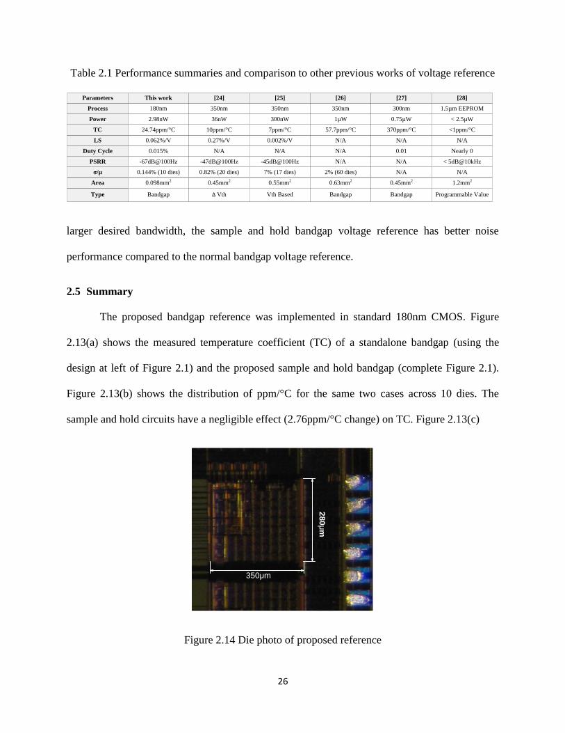
The proposed bandgap reference was implemented in standard 180nm CMOS. Figure
2.13(a) shows the measured temperature coefficient (TC) of a standalone bandgap (using the
design at left of Figure 2.1) and the proposed sample and hold bandgap (complete Figure 2.1).
Figure 2.13(b) shows the distribution of ppm/°C for the same two cases across 10 dies. The
sample and hold circuits have a negligible effect (2.76ppm/°C change) on TC. Figure 2.13(c)
350μm
28
0μm
Figure 2.14 Die photo of proposed reference

27
shows a histogram of bandgap output voltage across 10 dies. The single trimmed mean output
value is 1.1918V with of 1.713mV, and σ/μ of 0.144%.. Measured power supply rejection ratio
(PSRR) is also shown in Fig. 2.13(d). Since the only injection path is through the PMOS pass
transistor and kickback noise in the amplifier, PSRR is small throughout the entire frequency
range. The chip micrograph is given in Figure 2.14. Table 2.1 summarizes the testing results,
including a comparison to the most relevant prior work.
28
CHAPTER 3
Low Power ESD Clamp Circuits for Ultra Low Power
System
Robustness against electrostatic discharge (ESD) is a critical reliability issue in advanced
CMOS technologies. To prevent circuit damage due to ESD events (which can expose the circuit
to kV range voltages), ESD clamp circuits are typically incorporated in supply pad library cells.
These circuits use extremely wide devices (100s of μm) and thus exhibit leakage currents of 10nA
to 10μA (at 25°C and 125°C, respectively) despite the use of various low power approaches [18-
20, 31,32]. Recently, there has been increased interest in ultra-low power wireless sensor node
systems [6-12, 33] with constrained battery sizes and system standby power budgets as low as 10-
100nW. Considering the need for multiple power pads, these systems cannot use existing ESD
structures due to their high leakage, thereby compromising their reliability. To address this
M1
M2
M3
Detection
Node
M4
RC Node
Figure 3.1 Standard ESD schematic
29
challenge, we propose three ultra-low leakage ESD circuits that use special biasing structures to
reduce subthreshold leakage and gate-induced drain leakage (GIDL) while maintaining ESD
protection. In 180nm silicon test results, we demonstrate 10s of pA (nA) operation at room
temperature (125°C), which is a >100× improvement over prior state of the art.
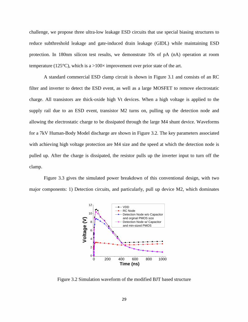
A standard commercial ESD clamp circuit is shown in Figure 3.1 and consists of an RC
filter and inverter to detect the ESD event, as well as a large MOSFET to remove electrostatic
charge. All transistors are thick-oxide high Vt devices. When a high voltage is applied to the
supply rail due to an ESD event, transistor M2 turns on, pulling up the detection node and
allowing the electrostatic charge to be dissipated through the large M4 shunt device. Waveforms
for a 7kV Human-Body Model discharge are shown in Figure 3.2. The key parameters associated
with achieving high voltage protection are M4 size and the speed at which the detection node is
pulled up. After the charge is dissipated, the resistor pulls up the inverter input to turn off the
clamp.
Figure 3.3 gives the simulated power breakdown of this conventional design, with two
major components: 1) Detection circuits, and particularly, pull up device M2, which dominates
0 200 400 600 800 10000
2
4
6
8
10
12
Vo
ltag
e (
V)
Time (ns)
VDD
RC Node
Detection Node w/o Capacitor
and orginal PMOS size
Detection Node w/ Capacitor
and min-sized PMOS
Figure 3.2 Simulation waveform of the modified BJT based structure
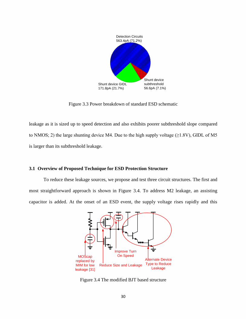
30
Detection Circuits
563.4pA (71.2%)
Shunt device GIDL
171.8pA (21.7%)
Shunt device
subthreshold
56.6pA (7.1%)
Figure 3.3 Power breakdown of standard ESD schematic
leakage as it is sized up to speed detection and also exhibits poorer subthreshold slope compared
to NMOS; 2) the large shunting device M4. Due to the high supply voltage (≥1.8V), GIDL of M5
is larger than its subthreshold leakage.
3.1 Overview of Proposed Technique for ESD Protection Structure
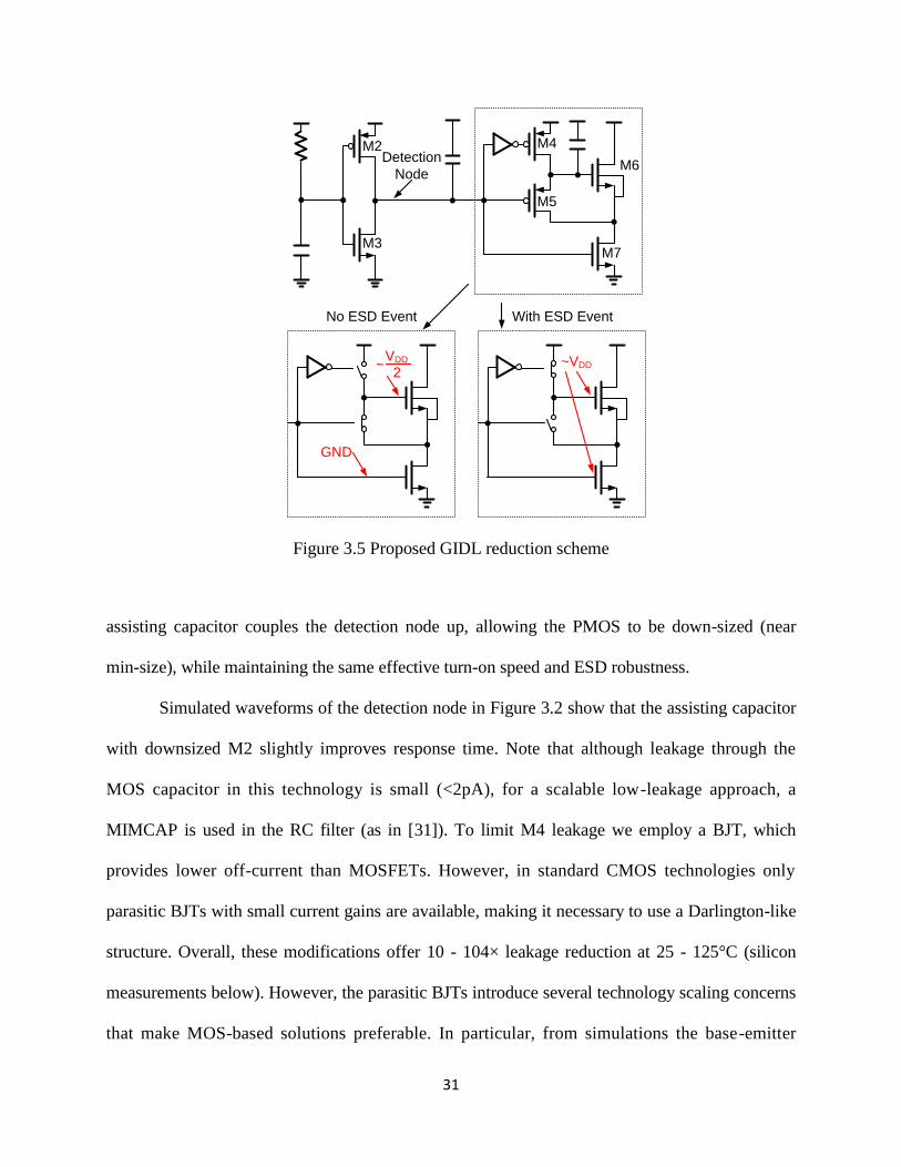
To reduce these leakage sources, we propose and test three circuit structures. The first and
most straightforward approach is shown in Figure 3.4. To address M2 leakage, an assisting
capacitor is added. At the onset of an ESD event, the supply voltage rises rapidly and this
Improve Turn
On Speed Alternate Device
Type to Reduce
LeakageReduce Size and Leakage
MOScap
replaced by
MIM for low
leakage [31]
Figure 3.4 The modified BJT based structure
31
Detection
Node
M2
M3
M4
M5
M6
M7
No ESD Event With ESD Event
~VDDVDD~
2
GND
Figure 3.5 Proposed GIDL reduction scheme
assisting capacitor couples the detection node up, allowing the PMOS to be down-sized (near
min-size), while maintaining the same effective turn-on speed and ESD robustness.
Simulated waveforms of the detection node in Figure 3.2 show that the assisting capacitor
with downsized M2 slightly improves response time. Note that although leakage through the
MOS capacitor in this technology is small (<2pA), for a scalable low-leakage approach, a
MIMCAP is used in the RC filter (as in [31]). To limit M4 leakage we employ a BJT, which
provides lower off-current than MOSFETs. However, in standard CMOS technologies only
parasitic BJTs with small current gains are available, making it necessary to use a Darlington-like
structure. Overall, these modifications offer 10 - 104× leakage reduction at 25 - 125°C (silicon
measurements below). However, the parasitic BJTs introduce several technology scaling concerns
that make MOS-based solutions preferable. In particular, from simulations the base-emitter
32
M4
M5
M6
M7
M8
M9
M10
A
B2VDD~3
VDD~3
VDD~
3
2VDD~3
-20 0 20 40 60 80 100 1200.0
0.6
1.2
1.8Node Voltage vs. Temperature
Vo
ltag
e (
V)
Temperature (C)
Node A
Node B
M1
M2
M3
Figure 3.6 GIDL reduction scheme for 3-stack (GIDL-1) with simulated internal node voltages
across temperature at 1.8V
current gain drops from 25 in 180nm to 5 in 65nm. Also, bipolar clamp snapback voltage
decreases with technology scaling more rapidly than MOSFETs [34], reducing effectiveness for
ESD protection.
3.2 Proposed Technique for ESD Protection Structure under CMOS Technology
Due to reason states in the end of section 3.1, we therefore also propose two MOS-based
structures that offer similar leakage reduction gains with better scalability and improved density.
A well-known approach to reduce MOSFET leakage is stacking, which yields a 2.9× subthreshold
leakage reduction in 180nm CMOS. However, as noted earlier, GIDL dominates leakage in the
shunt device and hence stacking alone only reduces total leakage by 17%.
The first method to address GIDL in an MOS shunt device is shown in Figure 3.5 and has
similarity with [35]. When there is no ESD event the gate and source of M6 are shorted and the
stacked shunt transistors M6 and M7 act as a voltage divider. As a result, the key GIDL parameter
Vdg is reduced by half for both transistors, lowering GIDL by 5.4×. When an ESD event occurs,
33
VDD
Detection
Node
@2 No ESD Event
M2
M3
M4
M5
M6
M7
M8
M9
M10
M11
M12
A
Figure 3.7 Leakage-based GIDL reduction methods (GIDL-2)
the two MOS shunts fully turn on to remove the electrostatic charge. The same concept can be
extended to a stack of 3 devices; simulations across temperature in Figure 3.6 show temperature
stability across a wide range (-20˚C to 125˚C). The 3-stack structure provides minimum leakage
for this approach (denoted GIDL-1). Further extending the method to a 4-stack degrades shunt on-
current, requiring device up-sizing for sufficient ESD protection and leading to higher leakage.
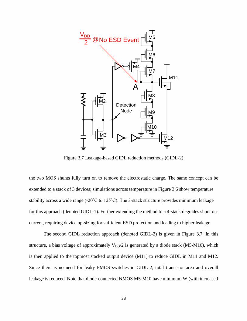
The second GIDL reduction approach (denoted GIDL-2) is given in Figure 3.7. In this
structure, a bias voltage of approximately VDD/2 is generated by a diode stack (M5-M10), which
is then applied to the topmost stacked output device (M11) to reduce GIDL in M11 and M12.
Since there is no need for leaky PMOS switches in GIDL-2, total transistor area and overall
leakage is reduced. Note that diode-connected NMOS M5-M10 have minimum W (with increased
34
15.3X
Node A~ VDD
2
-20 0 20 40 60 80 100 1200.0
0.6
1.2
1.8
Vo
lta
ge
(V
)
Temperature(C)
FF
SS
TT
0
200
400
600
800
GIDL-2
Le
ak
ag
e P
ow
er
(pW
) Detection Circuits
GIDL of Shunt Device
Subthreshold of Shunt Device
Standard ESD
Figure 3.8 Simulated internal node voltage across temperature and corners as well as leakage
power breakdown of GIDL-2
L) since they only need to overcome the subthreshold leakage of M4 and gate leakage of M11 to
maintain VDD/2 at node A. As a result, the diode stack leakage is negligible. Simulations across
temperature/process show the stability of node A voltage (Fig. 8). During an ESD event node A is
charged to VDD through M4 and then slowly discharges to VDD/2 through the diode stack. During
this relaxation time (350s in simulation) the ESD clamp experiences substantial GIDL. However,
since ESD events are rare, the impact on total energy is minimal and the low quiescent current of
the structure far outweighs it. Simulated leakage power breakdown of GIDL-2 is shown in Figure
3.8, showing a 15.3 - 115× reduction (25 - 125°C) compared to a conventional commercial clamp.
35
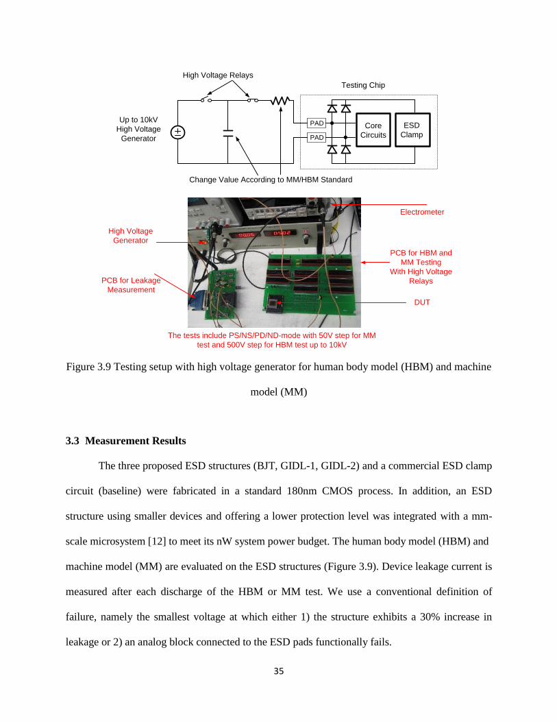
Up to 10kV
High Voltage
Generator
Core
CircuitsPAD
PAD ESD
Clamp
High Voltage Relays
Change Value According to MM/HBM Standard
Testing Chip
PCB for Leakage
Measurement
High Voltage
Generator
PCB for HBM and
MM Testing
With High Voltage
Relays
Electrometer
DUT
The tests include PS/NS/PD/ND-mode with 50V step for MM
test and 500V step for HBM test up to 10kV
Figure 3.9 Testing setup with high voltage generator for human body model (HBM) and machine
model (MM)
3.3 Measurement Results
The three proposed ESD structures (BJT, GIDL-1, GIDL-2) and a commercial ESD clamp
circuit (baseline) were fabricated in a standard 180nm CMOS process. In addition, an ESD
structure using smaller devices and offering a lower protection level was integrated with a mm-
scale microsystem [12] to meet its nW system power budget. The human body model (HBM) and
machine model (MM) are evaluated on the ESD structures (Figure 3.9). Device leakage current is
measured after each discharge of the HBM or MM test. We use a conventional definition of
failure, namely the smallest voltage at which either 1) the structure exhibits a 30% increase in
leakage or 2) an analog block connected to the ESD pads functionally fails.
36
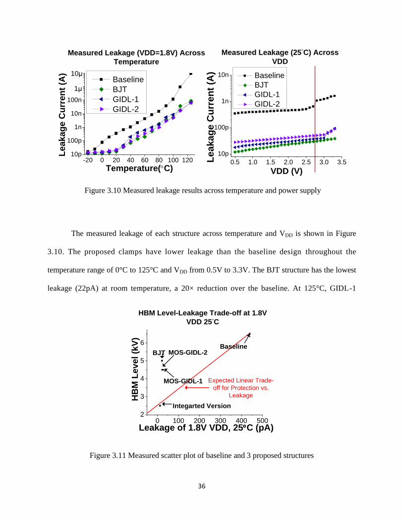
-20 0 20 40 60 80 100 12010p
100p
1n
10n
100n
1?
10?
Le
ak
ag
e C
urr
en
t (A
)
Temperature(C)
Baseline
BJT
GIDL-1
GIDL-2
Measured Leakage (VDD=1.8V) Across
Temperature
Measured Leakage (25˚C) Across
VDD
1μ
10μ
0.5 1.0 1.5 2.0 2.5 3.0 3.5
10p
100p
1n
10n
Leakag
e C
urr
en
t (A
)
VDD (V)
Baseline
BJT
GIDL-1
GIDL-2
Figure 3.10 Measured leakage results across temperature and power supply
The measured leakage of each structure across temperature and VDD is shown in Figure
3.10. The proposed clamps have lower leakage than the baseline design throughout the
temperature range of 0°C to 125°C and VDD from 0.5V to 3.3V. The BJT structure has the lowest
leakage (22pA) at room temperature, a 20× reduction over the baseline. At 125°C, GIDL-1
HBM Level-Leakage Trade-off at 1.8V
VDD 25˚C
Expected Linear Trade-
off for Protection vs.
Leakage
0 100 200 300 400 5002
3
4
5
6
Integarted Version
HB
M L
eve
l (k
V)
Leakage of 1.8V VDD, 25C (pA)
MOS-GIDL-2BJT
MOS-GIDL-1
Baseline
Figure 3.11 Measured scatter plot of baseline and 3 proposed structures
37
1.6 2.0 2.4 2.8 3.20
2
4
6
=1912pA
=317pA
Co
un
t
Leakage (nA)
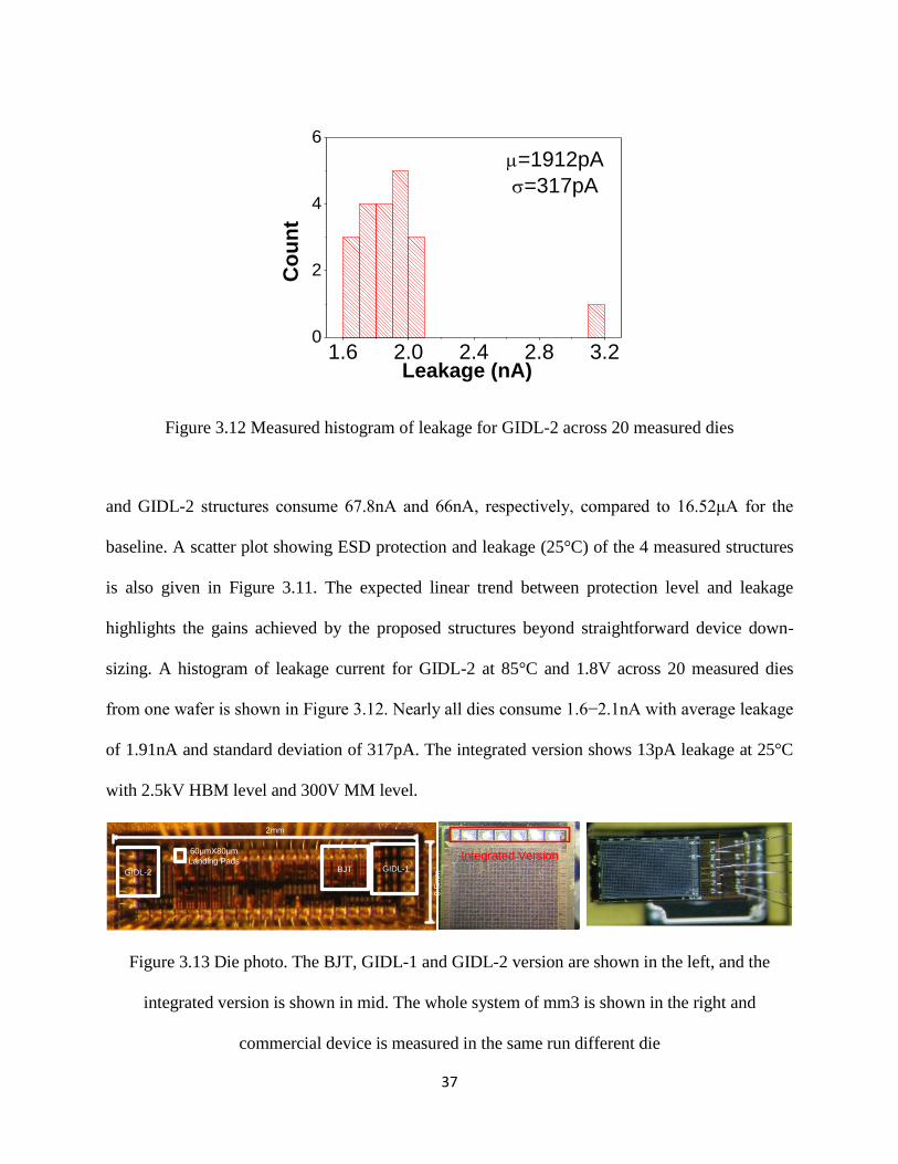
Figure 3.12 Measured histogram of leakage for GIDL-2 across 20 measured dies
and GIDL-2 structures consume 67.8nA and 66nA, respectively, compared to 16.52μA for the
baseline. A scatter plot showing ESD protection and leakage (25°C) of the 4 measured structures
is also given in Figure 3.11. The expected linear trend between protection level and leakage
highlights the gains achieved by the proposed structures beyond straightforward device down-
sizing. A histogram of leakage current for GIDL-2 at 85°C and 1.8V across 20 measured dies
from one wafer is shown in Figure 3.12. Nearly all dies consume 1.6−2.1nA with average leakage
of 1.91nA and standard deviation of 317pA. The integrated version shows 13pA leakage at 25°C
with 2.5kV HBM level and 300V MM level.
Integrated VersionGIDL-1GIDL-2 BJT
2mm
0.5
mm
60μmX80μm
Landing Pads
Figure 3.13 Die photo. The BJT, GIDL-1 and GIDL-2 version are shown in the left, and the
integrated version is shown in mid. The whole system of mm3 is shown in the right and
commercial device is measured in the same run different die
38
Table 3.1 Summary table of proposed ESD clamp circuits
ESD Structure Technology Area
(μm2)
HBM
Level (kV)
MM
Level (V)
Leakage
1.8V, 25˚C
Leakage
1.8V, 125˚C
Baseline
Commercial Clamp0.18μm 17500 6.5 400 440pA 9.18A
BJT 0.18μm 67200 5.0 350 22pA 88.1nA
GIDL-1 0.18μm 67200 4.5 400 28pA 67.8nA
GIDL-2 0.18μm 44800 4.5 400 24pA 66nA
Integrated Version
For mm3 system [12]0.18μm 35000 2.5 300 13pA 41nA
[18]* 65nm1029
(7891)**7.0 325 96nA (1V) 1.02A (1V)
[19] 65nm N/A 4.0 350 358nA (1V) 1.91A (1V)
[31]* 0.13μm N/A 6.5 400 N/A N/A
[32]* 65nm N/A >8.0 750 228nA (1V) 3.14A (1V)
* Uses special SCR devices
**Normalized to 0.18μm using ideal scaling
3.4 Summary
Overall the proposed GIDL-2 structure provides 18-139× leakage reduction over
commercial ESD clamps with 70-100% of ESD protection levels while avoiding special devices
such as SCR. Die photos are given in Fig. 3.13. Summary table is given in Table 3.1.

39
CHAPTER 4
Multiple-Choppers Technique to Increase the Noise
Efficiency of the Low Noise Amplifier
Recently, the recording of human body electrical signals has attracted growing attention.
Specifically, several low power high density recording devices have been proposed [36]-[38].
Although digital power consumption scales well with technology improvements, the noise
requirements of these systems restrict front-end amplifier power improvements due to the
fundamental noise efficiency factor (NEF) limits (fundamental limit = 1 with an ideal single
BJT amplifier). As a result the analog front-end power limits the number of channels in neural
recording arrays, effectively holding back major advances in brain machine interfaces.
4.1 Overview of the Fundamental Noise Limit of the Amplifier
The fundamental power consumption limit of the analog front-end amplifier arises from
the white noise of the input transistors. The amplifier NEF is given by:
𝑁𝐸𝐹 = 𝑉𝑟𝑚𝑠√2 × 𝐼𝑡𝑜𝑡𝑎𝑙
𝜋 × 𝑉𝑇 × 4𝑘𝑇 × 𝐵𝑎𝑛𝑑𝑤𝑖𝑑𝑡ℎ (4.1)
State-of-art neural recording systems typically employ high accuracy amplifiers with a
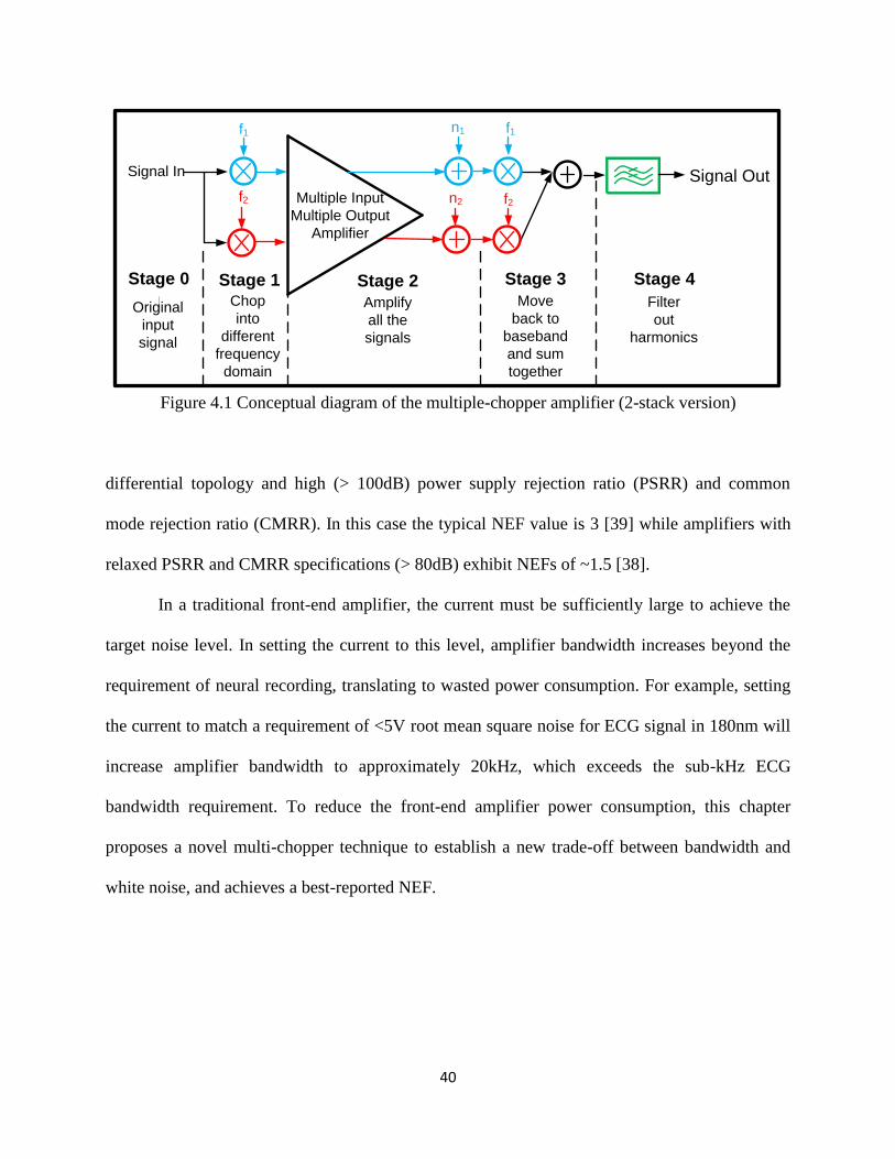
40
f1
f2 Multiple Input
Multiple Output
Amplifier
Signal In Signal Out
f1n1
f2n2
Stage 0
Original
input
signal
Stage 1Chop
into
different
frequency
domain
Stage 2
Amplify
all the
signals
Stage 3
Move
back to
baseband
and sum
together
Stage 4
Filter
out
harmonics
Figure 4.1 Conceptual diagram of the multiple-chopper amplifier (2-stack version)
differential topology and high (> 100dB) power supply rejection ratio (PSRR) and common
mode rejection ratio (CMRR). In this case the typical NEF value is 3 [39] while amplifiers with
relaxed PSRR and CMRR specifications (> 80dB) exhibit NEFs of ~1.5 [38].
In a traditional front-end amplifier, the current must be sufficiently large to achieve the
target noise level. In setting the current to this level, amplifier bandwidth increases beyond the
requirement of neural recording, translating to wasted power consumption. For example, setting
the current to match a requirement of <5V root mean square noise for ECG signal in 180nm will
increase amplifier bandwidth to approximately 20kHz, which exceeds the sub-kHz ECG
bandwidth requirement. To reduce the front-end amplifier power consumption, this chapter
proposes a novel multi-chopper technique to establish a new trade-off between bandwidth and
white noise, and achieves a best-reported NEF.
41
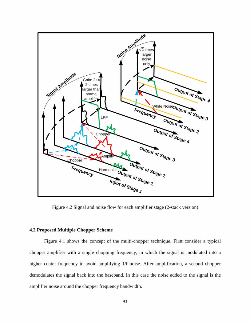
Noise A
mplit
ude
Input of Stage 1
Output of Stage 1
Output of Stage 2
ChopperAmplify
Harmonics
Output of Stage 3
ChopperOutput of Stage 4
LPF
Signal A
mplit
ude
Output of Stage 2
Output of Stage 3
Output of Stage 4
Frequency
White NoiseFrequency
Gain: 2×A
2 times
larger than
normal
amplifier
times
larger
noise
only
Figure 4.2 Signal and noise flow for each amplifier stage (2-stack version)
4.2 Proposed Multiple Chopper Scheme
Figure 4.1 shows the concept of the multi-chopper technique. First consider a typical
chopper amplifier with a single chopping frequency, in which the signal is modulated into a
higher center frequency to avoid amplifying 1/f noise. After amplification, a second chopper
demodulates the signal back into the baseband. In this case the noise added to the signal is the
amplifier noise around the chopper frequency bandwidth.

42
In the multi-chopper scheme, multiple chopper switches are used along with a multiple-
input / multiple-output current-reuse core amplifier. The target of the chopper here is both 1/f
noise and white Gaussian noise. The amplifier operates as follows: 1) The input signal is
modulated up into N different center frequencies by the different chopper switches (N=2 in
Figure 4.1 for clarity); 2) In the amplifying process, the signal is amplified by A for each of the
N center frequencies. The output signal consists of the signal, which is A times larger than the
input signal, plus the added amplifier noise at each center frequency; 3) Each chopper
demodulates the amplified signal and added noise back into the baseband frequency; 4) A
summing amplifier combines all N signals producing an output signal that is N×A times larger
than the input. However, as explained shortly, the summed noise sources are uncorrelated and
therefore sums only as √𝑁, providing the key benefit of the approach. Since the clock of the
chopper is a square wave rather than a sine wave the center frequencies are selected to be even
multiples, thus avoiding coinciding harmonics. Figure 4.2 shows the signal flow of the amplifier.
To quantify the benefits of the proposed scheme, the SNR improvement is calculated
assuming a flat gain A throughout the entire amplifying bandwidth: 1) for N different chopper
frequencies, the final output signal is N×A times larger. 2) Since the noise is uncorrelated in each
chopper frequency domain, the summing amplifier sums the power rather than voltage amplitude.
Hence, the power of the noise will be N times larger while the noise amplitude increases by only
√𝑁. 3) Since the gain of the signal is N×A while the gain in noise is √𝑁, the proposed scheme
improves SNR by √𝑁. The choice of the number of chopper switches represents a trade-off
between signal bandwidth (since the signal bandwidth f will be reduced by 1
2𝑁+1× and Gaussian
noise.
43
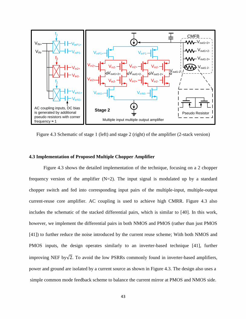
Vin2+ Vin2- Vin2+ Vin2-
VinN1+ VinN1-
Vout1+2+ Vout1+2- Vout1-2+Vout1-2-
Vin2+ Vin2- Vin2+ Vin2-
VinP1+ VinP1-
CMFB
VIN+
VIN-
f1
f1
f2
VinP1+
VinP1-
Vin2+
Vin2-
VinN1+
VinN1-
Vout1+2+
Vout1+2-
Vout1-2+
Vout1-2-
Pseudo Resistor
Multiple input multiple output amplifier
Stage 2AC coupling inputs, DC bias
is generated by additional
pseudo resistors with corner
frequency ≈ 1
Figure 4.3 Schematic of stage 1 (left) and stage 2 (right) of the amplifier (2-stack version)
4.3 Implementation of Proposed Multiple Chopper Amplifier
Figure 4.3 shows the detailed implementation of the technique, focusing on a 2 chopper
frequency version of the amplifier (N=2). The input signal is modulated up by a standard
chopper switch and fed into corresponding input pairs of the multiple-input, multiple-output
current-reuse core amplifier. AC coupling is used to achieve high CMRR. Figure 4.3 also
includes the schematic of the stacked differential pairs, which is similar to [40]. In this work,
however, we implement the differential pairs in both NMOS and PMOS (rather than just PMOS
[41]) to further reduce the noise introduced by the current reuse scheme; With both NMOS and
PMOS inputs, the design operates similarly to an inverter-based technique [41], further
improving NEF by√2. To avoid the low PSRRs commonly found in inverter-based amplifiers,
power and ground are isolated by a current source as shown in Figure 4.3. The design also uses a
simple common mode feedback scheme to balance the current mirror at PMOS and NMOS side.
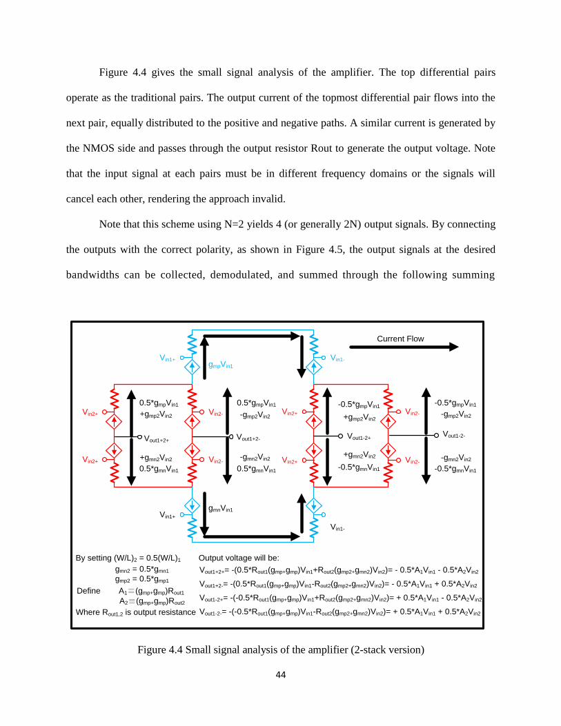
44
Figure 4.4 gives the small signal analysis of the amplifier. The top differential pairs
operate as the traditional pairs. The output current of the topmost differential pair flows into the
next pair, equally distributed to the positive and negative paths. A similar current is generated by
the NMOS side and passes through the output resistor Rout to generate the output voltage. Note
that the input signal at each pairs must be in different frequency domains or the signals will
cancel each other, rendering the approach invalid.
Note that this scheme using N=2 yields 4 (or generally 2N) output signals. By connecting
the outputs with the correct polarity, as shown in Figure 4.5, the output signals at the desired
bandwidths can be collected, demodulated, and summed through the following summing
Vin2+ Vin2- Vin2+ Vin2-
Vin1+ Vin1-gmpVin1
0.5*gmpVin1
+gmp2Vin2
0.5*gmpVin1
-gmp2Vin2
-0.5*gmpVin1
+gmp2Vin2
-0.5*gmpVin1
-gmp2Vin2
Vin2+ Vin2- Vin2+ Vin2-
Vin1+
Vin1-
gmnVin1
0.5*gmnVin1
+gmn2Vin2
0.5*gmnVin1
-gmn2Vin2
-0.5*gmnVin1
+gmn2Vin2
-0.5*gmnVin1
-gmn2Vin2
Vout1+2+Vout1+2- Vout1-2+
Vout1-2-
By setting (W/L)2 = 0.5(W/L)1
gmn2 = 0.5*gmn1
gmp2 = 0.5*gmp1
Vout1+2+= -(0.5*Rout1(gmp+gmp)Vin1+Rout2(gmp2+gmn2)Vin2)= - 0.5*A1Vin1 - 0.5*A2Vin2
Vout1+2-= -(0.5*Rout1(gmp+gmp)Vin1-Rout2(gmp2+gmn2)Vin2)= - 0.5*A1Vin1 + 0.5*A2Vin2
Vout1-2+= -(-0.5*Rout1(gmp+gmp)Vin1+Rout2(gmp2+gmn2)Vin2)= + 0.5*A1Vin1 - 0.5*A2Vin2
Vout1-2-= -(-0.5*Rout1(gmp+gmp)Vin1-Rout2(gmp2+gmn2)Vin2)= + 0.5*A1Vin1 + 0.5*A2Vin2
Define A1≡(gmp+gmp)Rout1
A2≡(gmp+gmp)Rout2
Current Flow
Where Rout1,2 is output resistance
Output voltage will be:
Figure 4.4 Small signal analysis of the amplifier (2-stack version)
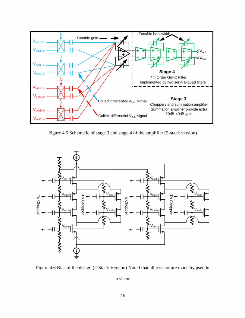
45
Vout1+2+
Vout1-2+
f1
Vout1+2-
Vout1-2-
f1
Vout1+2+
Vout1+2-
f2
Vout1-2+
Vout1-2-
f2
Vout+
Vout-
Stage 4
4th Order Gm-C Filter
Stage 3
Implemented by two serial Biquad filters
Collect differential Vout1 signal
Collect differential Vout2 signal
Choppers and summation amplifier
Summation amplifier provide extra
20dB-40dB gain
Tunable gainTunable bandwidth
Figure 4.5 Schematic of stage 3 and stage 4 of the amplifier (2-stack version)
Figure 4.6 Bias of the design (2-Stack Version) Noted that all resistor are made by pseudo
resistor
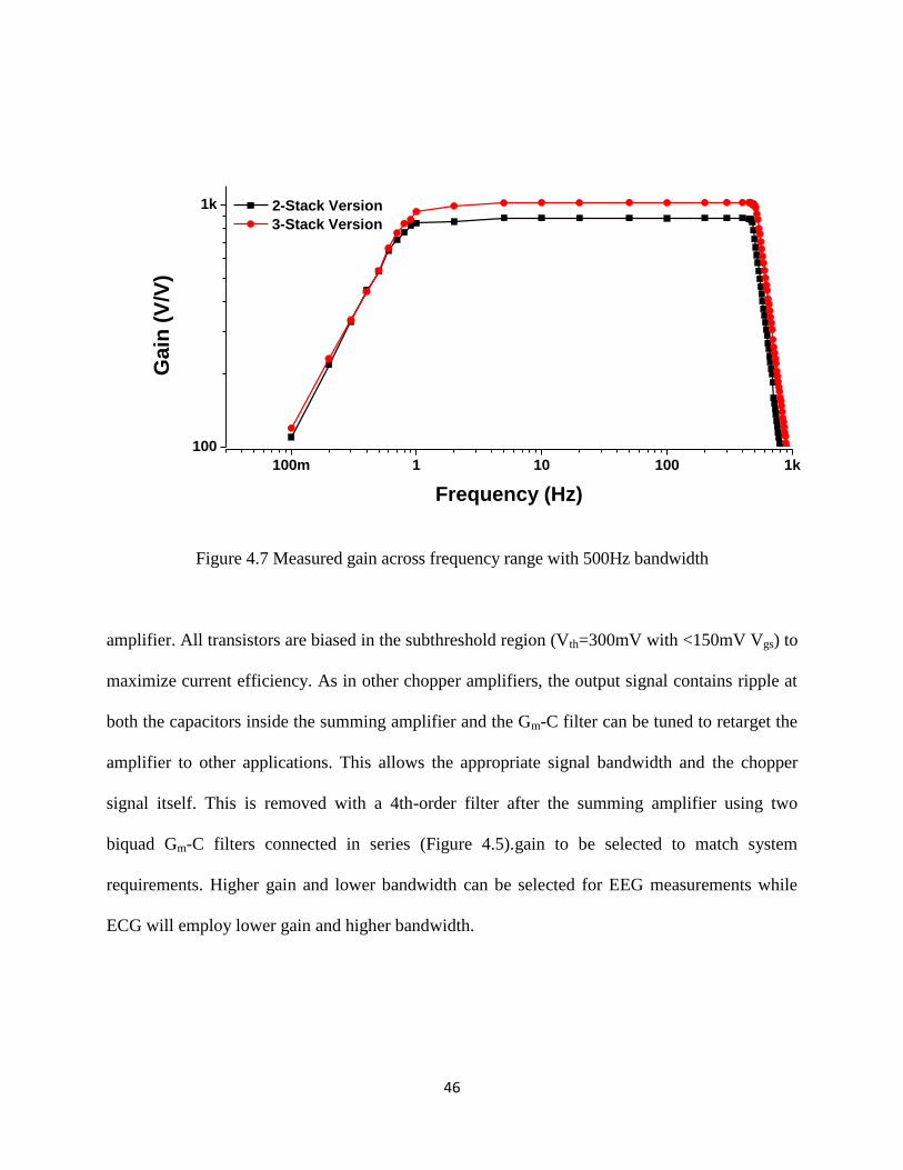
46
100m 1 10 100 1k
100
1k
Gain
(V
/V)
Frequency (Hz)
2-Stack Version
3-Stack Version
Figure 4.7 Measured gain across frequency range with 500Hz bandwidth
amplifier. All transistors are biased in the subthreshold region (Vth=300mV with <150mV Vgs) to
maximize current efficiency. As in other chopper amplifiers, the output signal contains ripple at
both the capacitors inside the summing amplifier and the Gm-C filter can be tuned to retarget the
amplifier to other applications. This allows the appropriate signal bandwidth and the chopper
signal itself. This is removed with a 4th-order filter after the summing amplifier using two
biquad Gm-C filters connected in series (Figure 4.5).gain to be selected to match system
requirements. Higher gain and lower bandwidth can be selected for EEG measurements while
ECG will employ lower gain and higher bandwidth.
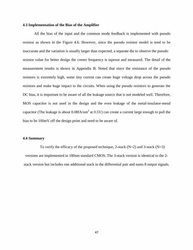
47
4.3 Implementation of the Bias of the Amplifier
All the bias of the input and the common mode feedback is implemented with pseudo
resistor as shown in the Figure 4.6. However, since the pseudo resistor model is tend to be
inaccurate and the variation is usually larger than expected, a separate die to observe the pseudo
resistor value for better design the corner frequency is tapeout and measured. The detail of the
measurement results is shown in Appendix B. Noted that since the resistance of the pseudo
resistors is extremely high, some tiny current can create huge voltage drop across the pseudo
resistors and make huge impact to the circuits. When using the pseudo resistors to generate the
DC bias, it is important to be aware of all the leakage source that is not modeled well. Therefore,
MOS capacitor is not used in the design and the even leakage of the metal-insulator-metal
capacitor (The leakage is about 0.08fA/um2 at 0.5V) can create a current large enough to pull the
bias to be 100mV off the design point and need to be aware of.
4.4 Summary
To verify the efficacy of the proposed technique, 2-stack (N=2) and 3-stack (N=3)
versions are implemented in 180nm standard CMOS. The 3-stack version is identical to the 2-
stack version but includes one additional stack in the differential pair and sums 8 output signals.
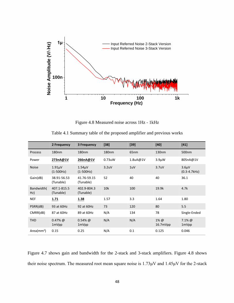
48
1 10 100 1k
100n
1μ
No
ise A
mp
litu
de (
V/
Hz)
Frequency (Hz)
Input Referred Noise 2-Stack Version
Input Referred Noise 3-Stack Version
Figure 4.8 Measured noise across 1Hz - 1kHz
Table 4.1 Summary table of the proposed amplifier and previous works
2 Frequency 3 Frequency [38] [39] [40] [41]
Process 180nm 180nm 180nm 65nm 130nm 500nm
Power 273nA@1V 266nA@1V 0.73uW 1.8uA@1V 3.9μW 805nA@1V
Noise 1.91μV(1-500Hz)
1.54μV(1-500Hz)
3.2uV 1uV 3.7uV 3.6μV(0.3-4.7kHz)
Gain(dB) 38.91-56.53(Tunable)
41.76-59.15(Tunable)
52 40 40 36.1
Bandwidth(Hz)
407.1-815.5(Tunable)
402.9-804.3(Tunable)
10k 100 19.9k 4.7k
NEF 1.71 1.38 1.57 3.3 1.64 1.80
PSRR(dB) 93 at 60Hz 92 at 60Hz 73 120 80 5.5
CMRR(dB) 87 at 60Hz 89 at 60Hz N/A 134 78 Single-Ended
THD 0.47% @ 1mVpp
0.54% @ 1mVpp
N/A N/A 1% @ 16.7mVpp
7.1% @ 1mVpp
Area(mm2) 0.15 0.25 N/A 0.1 0.125 0.046
Figure 4.7 shows gain and bandwidth for the 2-stack and 3-stack amplifiers. Figure 4.8 shows
their noise spectrum. The measured root mean square noise is 1.73μV and 1.45μV for the 2-stack
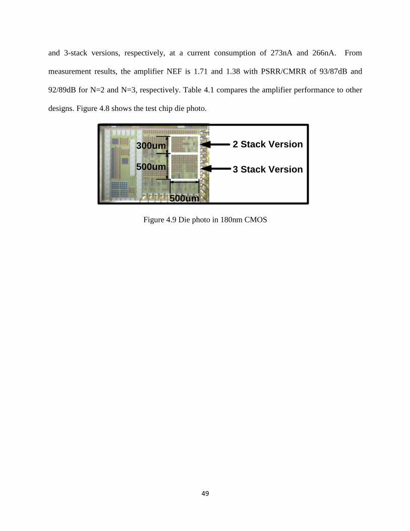
49
and 3-stack versions, respectively, at a current consumption of 273nA and 266nA. From
measurement results, the amplifier NEF is 1.71 and 1.38 with PSRR/CMRR of 93/87dB and
92/89dB for N=2 and N=3, respectively. Table 4.1 compares the amplifier performance to other
designs. Figure 4.8 shows the test chip die photo.
2 Stack Version
3 Stack Version500um
500um
300um
Figure 4.9 Die photo in 180nm CMOS
50
CHAPTER 5
An Injectable 64nW ECG Mixed-Signal SoC in 65nm
for Arrhythmia Monitoring
Electrocardiography (ECG) is the record of electrical activity in the heart and serves as a
critical source of information for the diagnosis and study of many heart disorders. Arrhythmia is
one of the most prevalent heart diseases; and in particular, according to a 2010 National
Institutes of Health report [42] 2.7 million people suffers from atrial fibrillation (AF), which is
the most common type of arrhythmia, and the number of people impacted continues to increase
over time [42].
In ECG waveform with AF, normal-shaped peaks (dubbed QRS complexes)
corresponding to the ventricles are seen, but with an irregular rhythm, but the peaks
corresponding to the atrial activity (dubbed P waves) are either abnormal in shape and/or size,
appear at fast irregular rates and/or non-discrete. Therefore, by monitoring the rate and shape
irregularities on the ECG, AF can be detected. However, arrhythmia can occur very rarely (e.g.,
only a few times a day) with each event lasting only for a handful of seconds. Consequently, in
arrhythmia studies and treatment, long-term but fast observation is essential to assess the
abnormality and its severity [43].
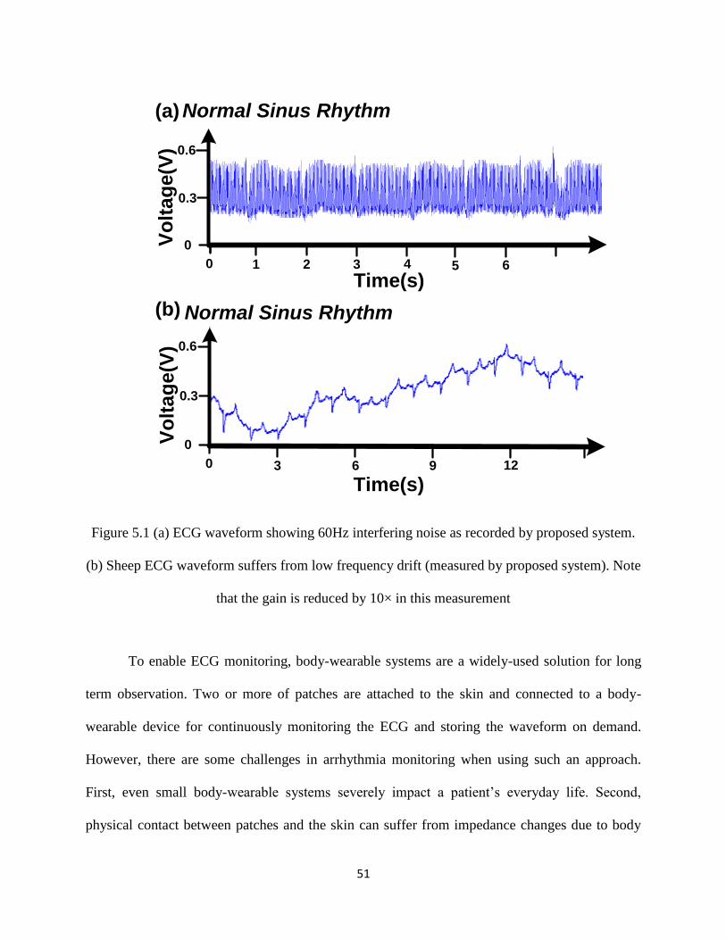
51
Normal Sinus Rhythm(a)
(b) Normal Sinus Rhythm
Time(s)1 2 3 4 5 60
Vo
lta
ge(V
) 0.6
0
0.3
Vo
lta
ge
(V) 0.6
0
0.3
Time(s)3 6 9 120
Figure 5.1 (a) ECG waveform showing 60Hz interfering noise as recorded by proposed system.
(b) Sheep ECG waveform suffers from low frequency drift (measured by proposed system). Note
that the gain is reduced by 10× in this measurement
To enable ECG monitoring, body-wearable systems are a widely-used solution for long
term observation. Two or more of patches are attached to the skin and connected to a body-
wearable device for continuously monitoring the ECG and storing the waveform on demand.
However, there are some challenges in arrhythmia monitoring when using such an approach.
First, even small body-wearable systems severely impact a patient’s everyday life. Second,
physical contact between patches and the skin can suffer from impedance changes due to body
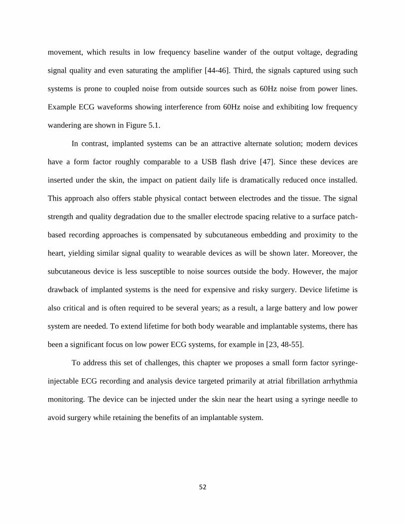
52
movement, which results in low frequency baseline wander of the output voltage, degrading
signal quality and even saturating the amplifier [44-46]. Third, the signals captured using such
systems is prone to coupled noise from outside sources such as 60Hz noise from power lines.
Example ECG waveforms showing interference from 60Hz noise and exhibiting low frequency
wandering are shown in Figure 5.1.
In contrast, implanted systems can be an attractive alternate solution; modern devices
have a form factor roughly comparable to a USB flash drive [47]. Since these devices are
inserted under the skin, the impact on patient daily life is dramatically reduced once installed.
This approach also offers stable physical contact between electrodes and the tissue. The signal
strength and quality degradation due to the smaller electrode spacing relative to a surface patch-
based recording approaches is compensated by subcutaneous embedding and proximity to the
heart, yielding similar signal quality to wearable devices as will be shown later. Moreover, the
subcutaneous device is less susceptible to noise sources outside the body. However, the major
drawback of implanted systems is the need for expensive and risky surgery. Device lifetime is
also critical and is often required to be several years; as a result, a large battery and low power
system are needed. To extend lifetime for both body wearable and implantable systems, there has
been a significant focus on low power ECG systems, for example in [23, 48-55].
To address this set of challenges, this chapter we proposes a small form factor syringe-
injectable ECG recording and analysis device targeted primarily at atrial fibrillation arrhythmia
monitoring. The device can be injected under the skin near the heart using a syringe needle to
avoid surgery while retaining the benefits of an implantable system.
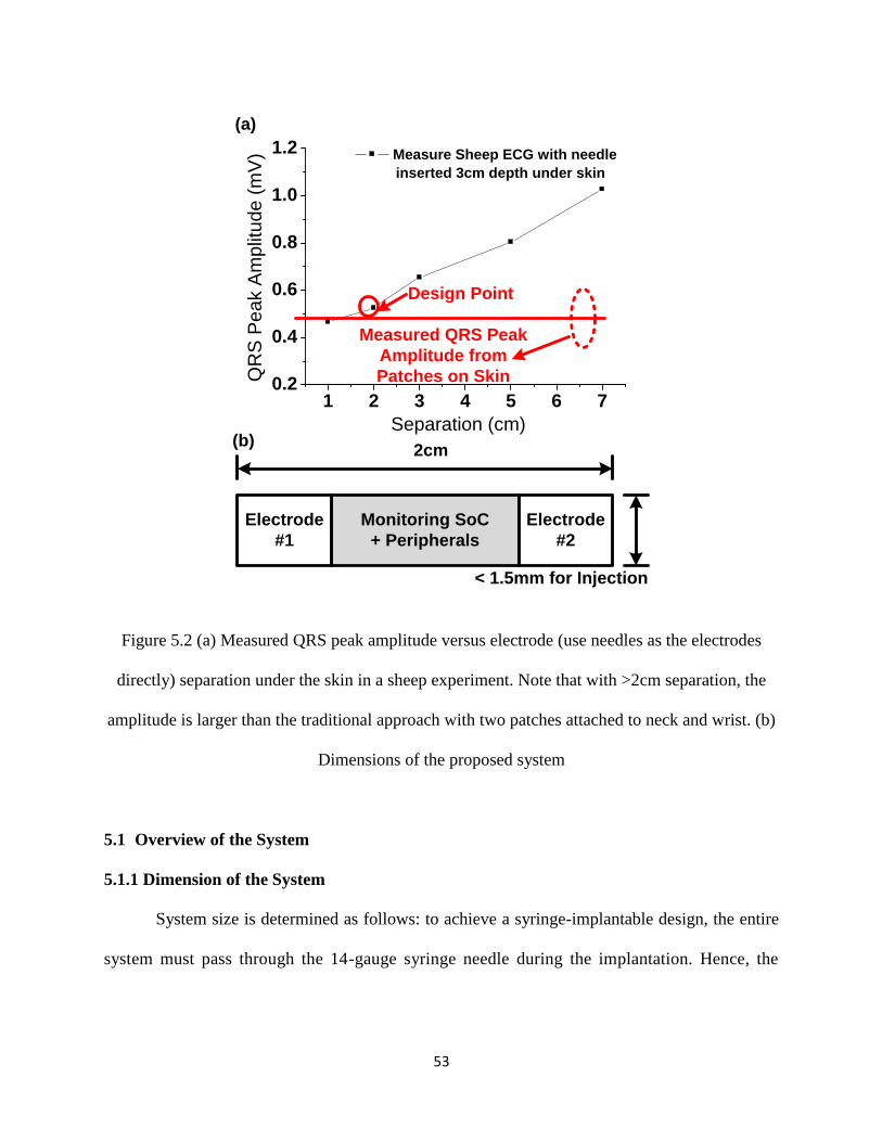
53
Monitoring SoC
+ Peripherals
Electrode
#1
Electrode
#2
< 1.5mm for Injection
2cm(b)
1 2 3 4 5 6 70.2
0.4
0.6
0.8
1.0
1.2 Measure Sheep ECG with needle
inserted 3cm depth under skin
QR
S P
ea
k A
mp
litu
de
(m
V)
Separation (cm)
(a)
Measured QRS Peak
Amplitude from
Patches on Skin
Design Point
Figure 5.2 (a) Measured QRS peak amplitude versus electrode (use needles as the electrodes
directly) separation under the skin in a sheep experiment. Note that with >2cm separation, the
amplitude is larger than the traditional approach with two patches attached to neck and wrist. (b)
Dimensions of the proposed system
5.1 Overview of the System
5.1.1 Dimension of the System
System size is determined as follows: to achieve a syringe-implantable design, the entire
system must pass through the 14-gauge syringe needle during the implantation. Hence, the
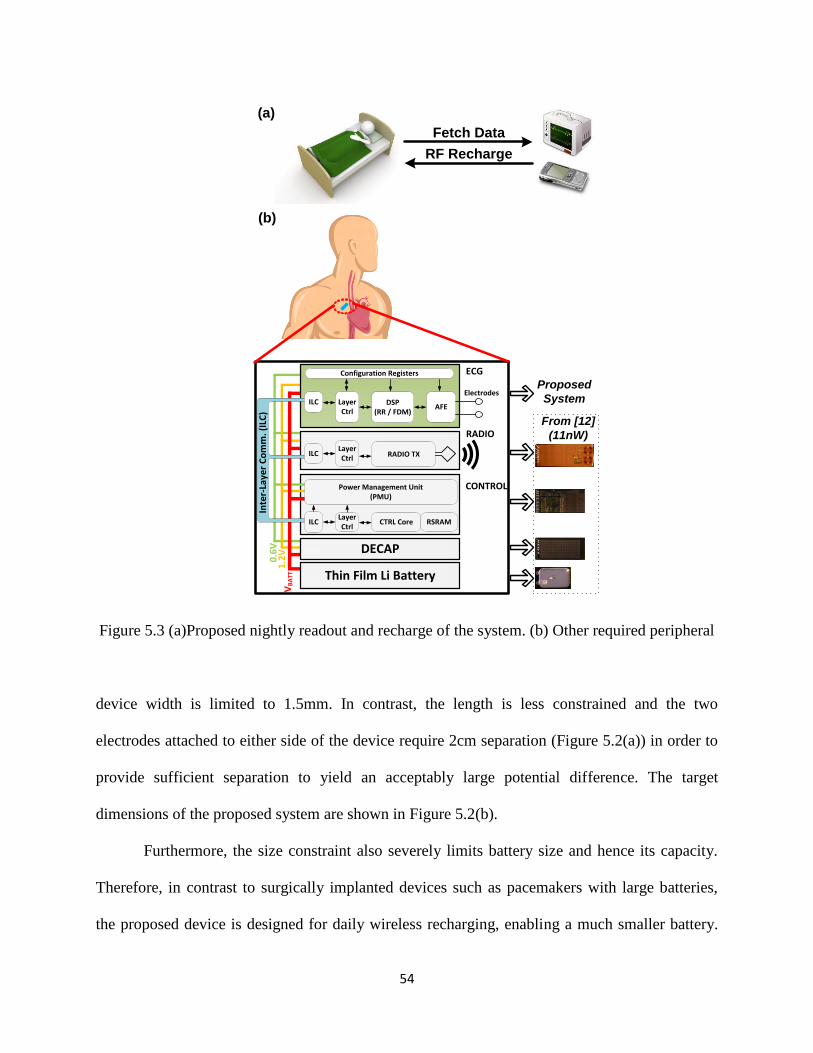
54
Fetch Data
RF Recharge
(a)
ECG
DSP(RR / FDM)
RADIO TX
CTRL Core RSRAM
RADIO
CONTROL
LayerCtrl
LayerCtrl
LayerCtrl
AFE
0.6
V1
.2V
Power Management Unit (PMU)
VB
ATT
Configuration Registers
Thin Film Li Battery
DECAP
Inte
r-La
yer
Co
mm
. (IL
C)
ILC
ILC
ILC
Electrodes
From [12]
(11nW)
Proposed
System
(b)
Figure 5.3 (a)Proposed nightly readout and recharge of the system. (b) Other required peripheral
device width is limited to 1.5mm. In contrast, the length is less constrained and the two
electrodes attached to either side of the device require 2cm separation (Figure 5.2(a)) in order to
provide sufficient separation to yield an acceptably large potential difference. The target
dimensions of the proposed system are shown in Figure 5.2(b).
Furthermore, the size constraint also severely limits battery size and hence its capacity.
Therefore, in contrast to surgically implanted devices such as pacemakers with large batteries,
the proposed device is designed for daily wireless recharging, enabling a much smaller battery.

55
While the patient sleeps, a host station (depicted in Figure 5.3(a)) near the bed could recharge
and retrieve the stored data through a wireless channel. The lifetime between recharging is set to
be 5 days to provide a safety margin. Matching battery size to device size allows for a 5uA*hr,
3.7mm2 Li battery, which constrains system power consumption to be less than 167nW. This
represents a challenging power constraint given that comparable systems in the literature
typically consume 1~30µW [23, 48-54].
5.1.2 System Overview
The proposed ECG monitoring SoC is 1.4mm wide and consumes 64nW while
continuously monitoring for arrhythmia. The ability of the system is focus on low power
consumption and arrhythmia monitoring depends in part on efficient algorithms. The system
consists of analog signal acquisition and digital back end blocks. The signal from electrodes is
filtered, amplified, and converted to the digital domain by an analog front end (AFE). A digital
signal processing (DSP) module analyzes the waveform within a 10-second search window and
detects abnormal cardiac events. Whenever an abnormal event is detected, the device stores the
current search window waveform (10× down sampled) into local memory; it can then be
transferred to an external device through means such as a wireless transceiver for further analysis
by clinicians. It is also compatible with other ultra-low power sensor node peripherals as shown
in Figure 5.3(b) [12].
5.2 Implementation of the AFE
Figure 5.4 shows the AFE top level block diagram. The AFE consists of three blocks: a
low noise instrumentation amplifier (LNA), a variable gain amplifier (VGA), and a successive
approximation register analog-to-digital converter (SAR ADC). To reduce power consumption,
56
In+
In-
Low Noise
Amplifer
Variable Gain
Amplifier
DAC
Sample
and Hold
SAR Logic
Comparator
Digital Back End
Successive Approximation Registers
Analog-Digital Converter
Tuning Gain and
Noise Level
Analog Front End
ADC output
Anti
Aliasing
Filter
Figure 5.4 Top level diagram of the analog front end.
the AFE supply voltage is 0.6V and all building blocks except the ADCs clocked comparator are
biased in the subthreshold regime for low power and high current efficiency. Note that the low
supply voltage may incur non-linearity in the final output signal, especially in the amplifier stage.
However, based on simulation results final arrhythmia detection is unaffected with <3.5% (THD)
nonlinearity. Therefore, the nonlinearity design target is set to 3% for the AFE to best balance
system performance and power consumption.
5.2.1 Noise Specification
Similar to other noise-limited amplifier designs [38], the total power consumption of the
analog front end is dominated by the first stage of the LNA. Typical ECG designs usually target
extremely low input referred noise level (around 3 µV [56-57]; see red dashed line in Figure
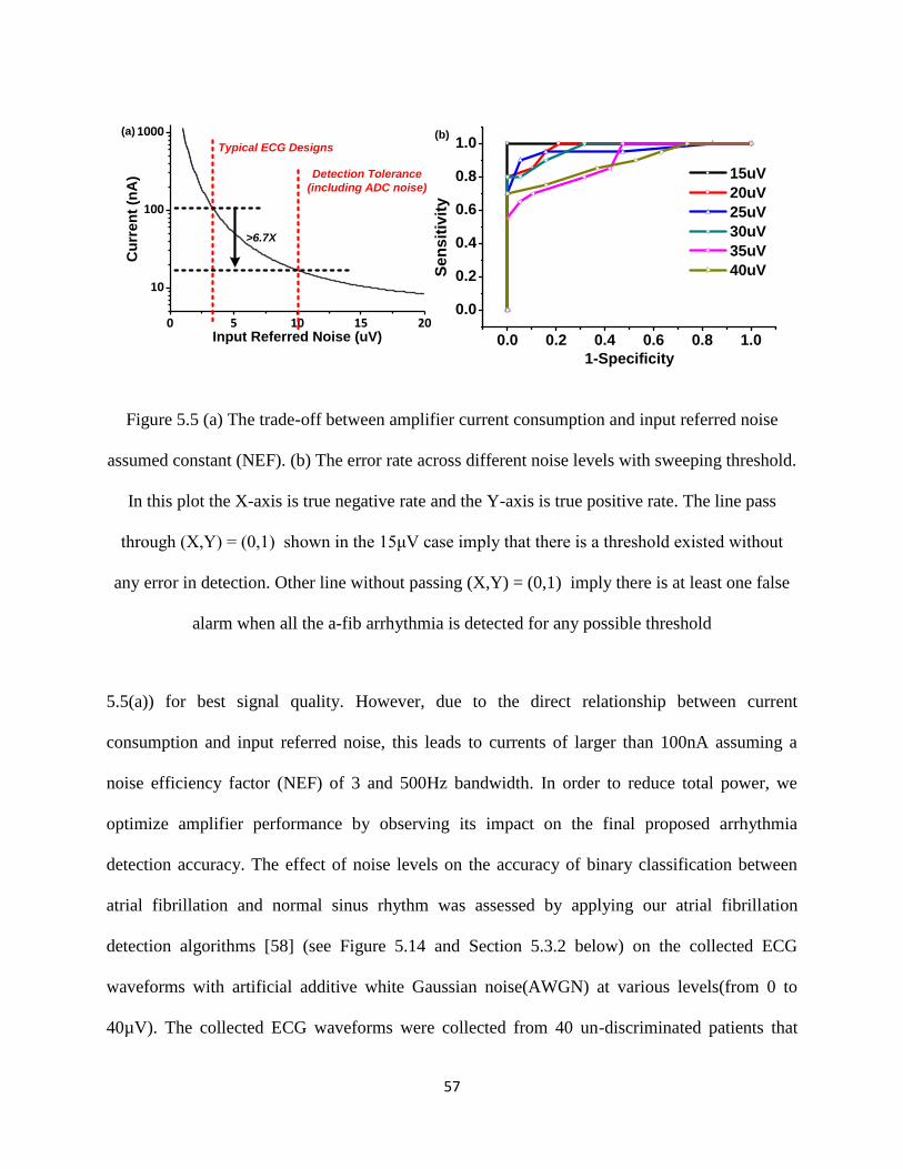
57
0 5 10 15 20
10
100
1000C
urr
en
t (n
A)
Input Referred Noise (uV)
Typical ECG Designs
Detection Tolerance
(including ADC noise)
>6.7X
0.0 0.2 0.4 0.6 0.8 1.0
0.0
0.2
0.4
0.6
0.8
1.0
Se
ns
itiv
ity
1-Specificity
15uV
20uV
25uV
30uV
35uV
40uV
(a) (b)
Figure 5.5 (a) The trade-off between amplifier current consumption and input referred noise
assumed constant (NEF). (b) The error rate across different noise levels with sweeping threshold.
In this plot the X-axis is true negative rate and the Y-axis is true positive rate. The line pass
through (X,Y) = (0,1) shown in the 15μV case imply that there is a threshold existed without
any error in detection. Other line without passing (X,Y) = (0,1) imply there is at least one false
alarm when all the a-fib arrhythmia is detected for any possible threshold
5.5(a)) for best signal quality. However, due to the direct relationship between current
consumption and input referred noise, this leads to currents of larger than 100nA assuming a
noise efficiency factor (NEF) of 3 and 500Hz bandwidth. In order to reduce total power, we
optimize amplifier performance by observing its impact on the final proposed arrhythmia
detection accuracy. The effect of noise levels on the accuracy of binary classification between
atrial fibrillation and normal sinus rhythm was assessed by applying our atrial fibrillation
detection algorithms [58] (see Figure 5.14 and Section 5.3.2 below) on the collected ECG
waveforms with artificial additive white Gaussian noise(AWGN) at various levels(from 0 to
40µV). The collected ECG waveforms were collected from 40 un-discriminated patients that
58
were referred to the University of Michigan hospital for diagnosis and treatment of atrial
fibrillation and the noise levels added was designed to surpass the typical ECG noise level
(ECGs were recorded during an EP procedure under supine and sedation condition by an EP-
Med System (St. Jude Medical, St. Paul, Minn.)). Figure 5.5(a) shows that with a relaxed noise
constraint, AFE power consumption reduces significantly, but the Receiver Operating
Characteristics curves in Figure 5.5(b) demonstrate that the detection accuracy drops as well.
Nevertheless, the proposed system and detection algorithm suffers no performance degradation
(100% sensitivity and specificity) with up to 15 µV input referred noise. As a result the design is
targeted to 15µV input referred noise to minimize power consumption while maintaining high
atrial fibrillation detection accuracy. In the final design, the amplifier specification is tightened to
10µV input referred noise across process corners to allow for a 10µV ADC noise budget. This
optimization reduces AFE power by 6.7× from 132nW to 17nW and system power by 2.45×
from 177nW to 72nW, compared to typical ECG signal acquisition designs that require noise
levels of ≤ 3µV. Due to the resulting high performance variability and the possibility of the
environmental and process changes, the amplifier gain, bandwidth, and input referred noise can
be adjusted by the digital blocks to maximize the useful signal range.
5.2.2 Amplifier Implementation
As shown in the AFE top level diagram, two amplifiers are used in series to provide low noise
and high gain. The first amplifier focuses on low noise while the second amplifier enables
tunable gain. Due to the large tissue-electrode impedance (measured to vary from 1MΩ to
5MΩacross different instances of the same model of electrodes, with ~4 MΩ average) the input
amplifier requires very high input impedance. In addition, the signal is located in the flicker
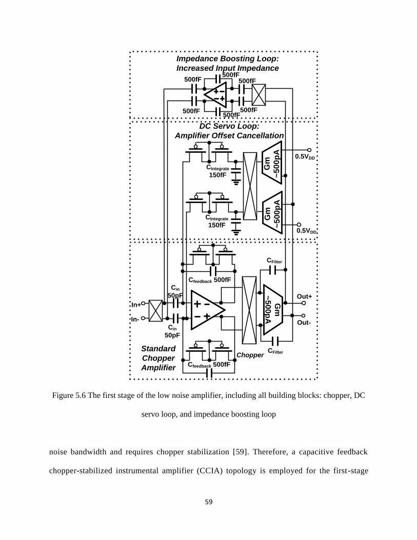
59
In+
In-
CFilter
CFilter
0.5VDD
CIntegrate
150fF
Impedance Boosting Loop:
Increased Input Impedance
Chopper
Out+
Out-
Cin
50pF
Cin
50pF
Standard
Chopper
Amplifier
Cfeedback 500fF
Cfeedback 500fF
0.5VDD
Gm
~5
00
pA
Gm
~5
00
pA
DC Servo Loop:
Amplifier Offset Cancellation
Gm
~5
00
pA
CIntegrate
150fF
500fF
500fF 500fF
500fF
500fF
500fF
Figure 5.6 The first stage of the low noise amplifier, including all building blocks: chopper, DC
servo loop, and impedance boosting loop
noise bandwidth and requires chopper stabilization [59]. Therefore, a capacitive feedback
chopper-stabilized instrumental amplifier (CCIA) topology is employed for the first -stage
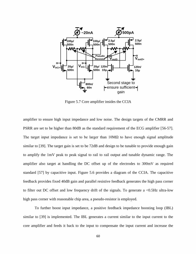
60
Vin1+Vin1-
~20nA 500pA
Vout2-
Second stage to
ensure sufficient
gain
Vout2+
100μ/
500n
100μ/
500n
20μ/
500n
20μ/
500n
800n/
60n
2.5μ/
500n
2.5μ/
500n
120n/
10μ
120n/
10μ
Pseudo
Resistor
Figure 5.7 Core amplifier insides the CCIA
amplifier to ensure high input impedance and low noise. The design targets of the CMRR and
PSRR are set to be higher than 80dB as the standard requirement of the ECG amplifier [56-57].
The target input impedance is set to be larger than 10MΩ to have enough signal amplitude
similar to [39]. The target gain is set to be 72dB and design to be tunable to provide enough gain
to amplify the 1mV peak to peak signal to rail to rail output and tunable dynamic range. The
amplifier also target at handling the DC offset up of the electrodes to 300mV as required
standard [57] by capacitive input. Figure 5.6 provides a diagram of the CCIA. The capacitive
feedback provides fixed 40dB gain and parallel resistive feedback generates the high pass corner
to filter out DC offset and low frequency drift of the signals. To generate a <0.5Hz ultra-low
high pass corner with reasonable chip area, a pseudo-resistor is employed.
To further boost input impedance, a positive feedback impedance boosting loop (IBL)
similar to [39] is implemented. The IBL generates a current similar to the input current to the
core amplifier and feeds it back to the input to compensate the input current and increase the
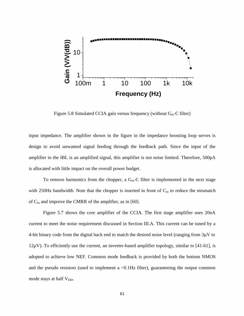
61
100m 1 10 100 1k 10k
1
10
Ga
in (
V/V
(dB
))
Frequency (Hz)
Figure 5.8 Simulated CCIA gain versus frequency (without Gm-C filter)
input impedance. The amplifier shown in the figure in the impedance boosting loop serves is
design to avoid unwanted signal feeding through the feedback path. Since the input of the
amplifier in the IBL is an amplified signal, this amplifier is not noise limited. Therefore, 500pA
is allocated with little impact on the overall power budget.
To remove harmonics from the chopper, a Gm-C filter is implemented in the next stage
with 250Hz bandwidth. Note that the chopper is inserted in front of Cin to reduce the mismatch
of Cin and improve the CMRR of the amplifier, as in [60].
Figure 5.7 shows the core amplifier of the CCIA. The first stage amplifier uses 20nA
current to meet the noise requirement discussed in Section III.A. This current can be tuned by a
4-bit binary code from the digital back end to match the desired noise level (ranging from 3µV to
12µV). To efficiently use the current, an inverter-based amplifier topology, similar to [41-61], is
adopted to achieve low NEF. Common mode feedback is provided by both the bottom NMOS
and the pseudo resistors (used to implement a <0.1Hz filter), guaranteeing the output common
mode stays at half VDD.
62
Table 5.1 Simulated specifications of the CCIA together with Gm-C filter
Midband Gain
Input Referred Noise
offset
PSRR
CMRR
36.92dB
8.4uV (with chopper)
5.8uV(without chopper)
1.52mV (without DSL)
>80dB for < 500Hz
>80dB for < 500Hz
VDD 0.6V
High 3dB 547.7Hz
NEF 2.258
Input Impedance> 110 MΩ (with IBL)
Topology CCIA
Low 3dB 0.117Hz
THD 2.24%
> 10 MΩ (without IBL)
0.071mV (with DSL)
From simulation, the first stage amplifier gain is 32dB, which is not sufficient to provide
the overall 40dB gain target through the feedback network. Therefore, a second amplifier stage is
required within the core amplifier. Since the subsequent amplifier receives an amplified signal,
the noise constraint is significantly relaxed; this stage consumes only 500pA and allows the
CCIA to achieve 61dB gain overall. Simulation results of the CCIA overall gain are shown in
Figure 5.8.
A common issue with inverter-based amplifier design is vulnerability of the bias point to
PVT variations. Therefore, a DC servo loop (DSL), similar to [39], is adopted to stabilize the
differential output and reduce offset by fixing the DC output to half VDD. From simulation
results, the DSL reduces DC offset from 1.52mV to 0.071mV.
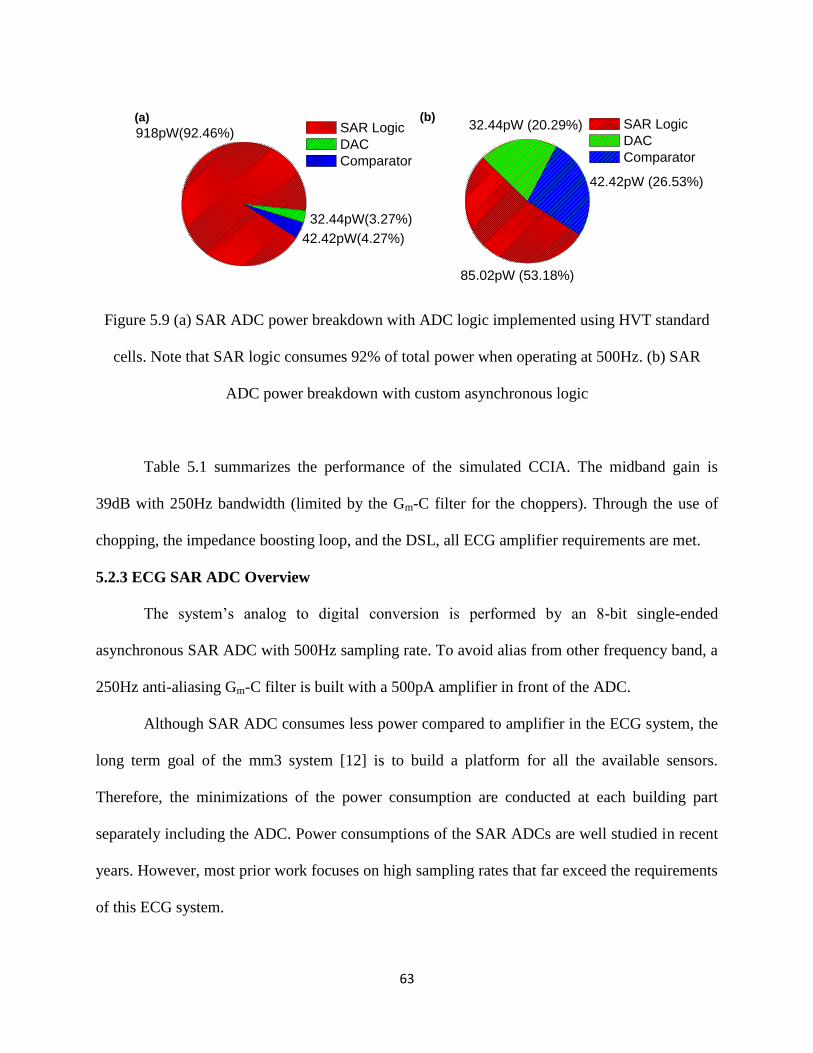
63
32.44pW(3.27%)
42.42pW(4.27%)
SAR Logic
DAC
Comparator
918pW(92.46%)
(a) (b)
42.42pW (26.53%)
32.44pW (20.29%)
85.02pW (53.18%)
SAR Logic
DAC
Comparator
Figure 5.9 (a) SAR ADC power breakdown with ADC logic implemented using HVT standard
cells. Note that SAR logic consumes 92% of total power when operating at 500Hz. (b) SAR
ADC power breakdown with custom asynchronous logic
Table 5.1 summarizes the performance of the simulated CCIA. The midband gain is
39dB with 250Hz bandwidth (limited by the Gm-C filter for the choppers). Through the use of
chopping, the impedance boosting loop, and the DSL, all ECG amplifier requirements are met.
5.2.3 ECG SAR ADC Overview
The system’s analog to digital conversion is performed by an 8-bit single-ended
asynchronous SAR ADC with 500Hz sampling rate. To avoid alias from other frequency band, a
250Hz anti-aliasing Gm-C filter is built with a 500pA amplifier in front of the ADC.
Although SAR ADC consumes less power compared to amplifier in the ECG system, the
long term goal of the mm3 system [12] is to build a platform for all the available sensors.
Therefore, the minimizations of the power consumption are conducted at each building part
separately including the ADC. Power consumptions of the SAR ADCs are well studied in recent
years. However, most prior work focuses on high sampling rates that far exceed the requirements
of this ECG system.
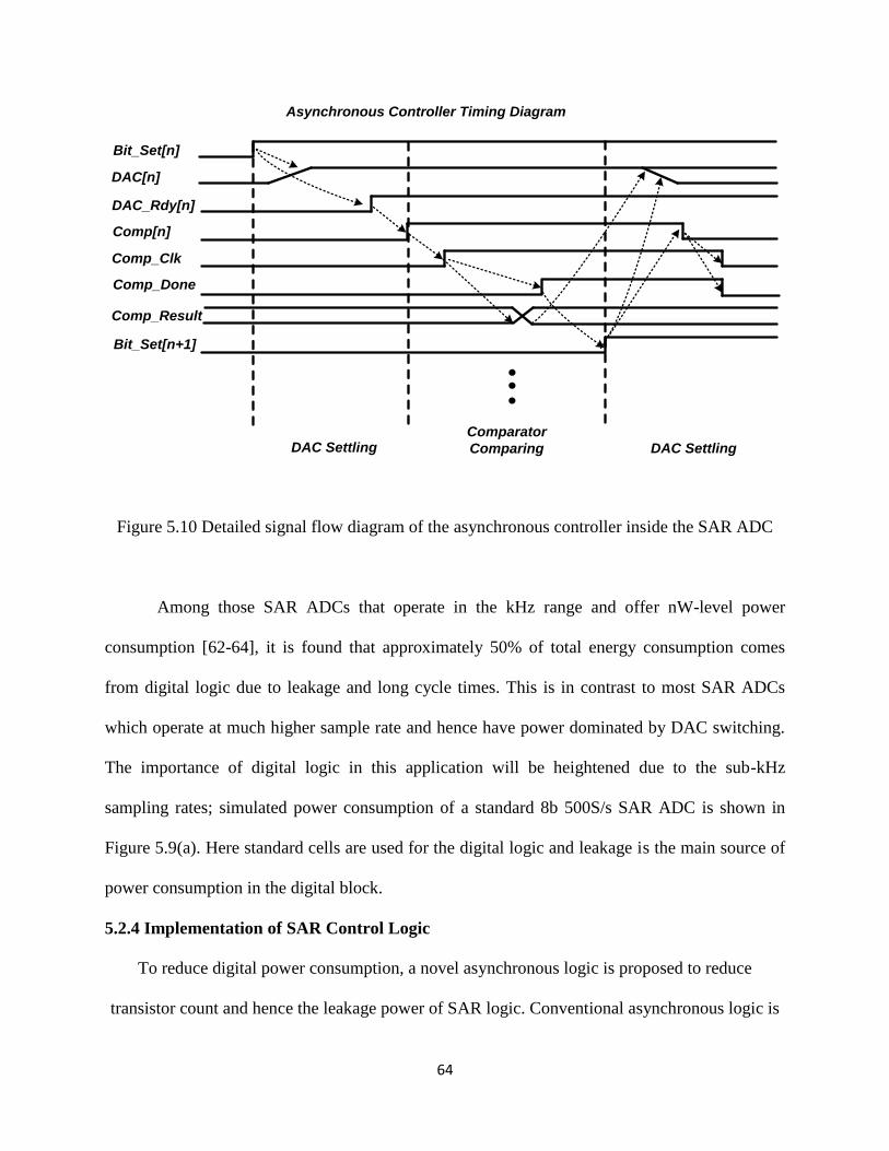
64
Bit_Set[n]
DAC_Rdy[n]
DAC[n]
Comp[n]
Comp_Clk
Comp_Done
Bit_Set[n+1]
Comp_Result
Asynchronous Controller Timing Diagram
DAC SettlingComparator
Comparing DAC Settling
Figure 5.10 Detailed signal flow diagram of the asynchronous controller inside the SAR ADC
Among those SAR ADCs that operate in the kHz range and offer nW-level power
consumption [62-64], it is found that approximately 50% of total energy consumption comes
from digital logic due to leakage and long cycle times. This is in contrast to most SAR ADCs
which operate at much higher sample rate and hence have power dominated by DAC switching.
The importance of digital logic in this application will be heightened due to the sub-kHz
sampling rates; simulated power consumption of a standard 8b 500S/s SAR ADC is shown in
Figure 5.9(a). Here standard cells are used for the digital logic and leakage is the main source of
power consumption in the digital block.
5.2.4 Implementation of SAR Control Logic
To reduce digital power consumption, a novel asynchronous logic is proposed to reduce
transistor count and hence the leakage power of SAR logic. Conventional asynchronous logic is
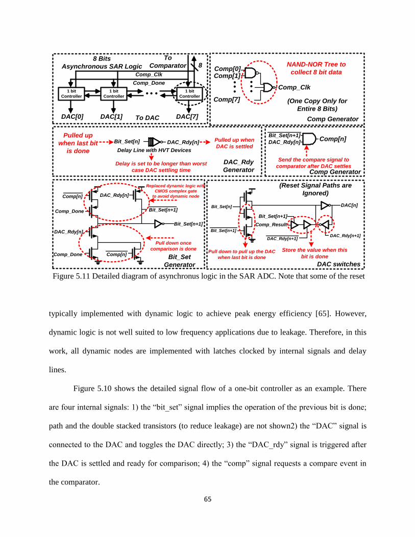
65
1 bit
Controller
1 bit
Controller
1 bit
Controller
To
Comparator 8
To DAC
8 Bits
Asynchronous SAR Logic
DAC[0] DAC[1] DAC[7]
(Reset Signal Paths are
Ignored)
Bit_Set[n]
Bit_Set[n+1]
DAC[n]
Bit_Set[n+1]
DAC_Rdy[n+1]DAC_Rdy[n+1]
Comp_Result
Bit_Set[n] DAC_Rdy[n] DAC_Rdy[n]
Bit_Set[n+1]Comp[n]
Bit_Set[n+1]
Comp[n]
Comp_Done
DAC_Rdy[n]
DAC_Rdy[n]
Comp_Done Comp[n]
Bit_Set[n+1]
Delay Line with HVT Devices
Delay is set to be longer than worst
case DAC settling time
Replaced dynamic logic with
CMOS complex gate
to avoid dynamic node
Pulled up
when last bit
is done
Pulled up when
DAC is settled
Pull down to pull up the DAC
when last bit is done
Store the value when this
bit is done
Pull down once
comparison is done
Send the compare signal to
comparator after DAC settles
Comp[0]Comp[1]
Comp[7]
Comp_Clk
(One Copy Only for
Entire 8 Bits)
Bit_Set
Generator DAC switches
Comp Generator
DAC_Rdy
Generator
NAND-NOR Tree to
collect 8 bit data
Comp Generator
Comp_Done
Comp_Clk
Figure 5.11 Detailed diagram of asynchronus logic in the SAR ADC. Note that some of the reset
typically implemented with dynamic logic to achieve peak energy efficiency [65]. However,
dynamic logic is not well suited to low frequency applications due to leakage. Therefore, in this
work, all dynamic nodes are implemented with latches clocked by internal signals and delay
lines.
Figure 5.10 shows the detailed signal flow of a one-bit controller as an example. There
are four internal signals: 1) the “bit_set” signal implies the operation of the previous bit is done;
path and the double stacked transistors (to reduce leakage) are not shown2) the “DAC” signal is
connected to the DAC and toggles the DAC directly; 3) the “DAC_rdy” signal is triggered after
the DAC is settled and ready for comparison; 4) the “comp” signal requests a compare event in
the comparator.
66
Once the result of the last bit comparison is done, the “bit_set” signal is pulled up by the
previous stage. The circuit to pull up the “bit_set” signal is shown at bottom left of Figure 5.11.
The “DAC” signal is then set to 1 by the circuit shown in the bottom right of Figure 5.11 (note
that the DAC is set to 0 initially and floating nodes are completely avoided through the use of
latches). Once the DAC is settled, “DAC_rdy” goes high. Since direct detection of the DAC
settling to 8 bit accuracy would consume significant energy, the circuit triggering the “DAC_rdy”
signal is implemented with a delay line set to be longer than the expected DAC settling time
across all corners. Since a long delay line can also consume high power, I/O HVT devices are
used to reduce the number of stages and save power. Once the DAC has settled, the “Comp”
signal goes high and sends a comparator clock signal to trigger the comparison. After the
comparison result is generated, “comp_result” and “comp_done” are sent by the comparator. The
controller saves the result into the DAC and raises the “bit_set” signal for the next stage.
The transistors count of the proposed design is 34 compared to the 48 transistors of the
traditional 2 DFF design and 29% of reduction is achieved. To further reduce power all leakage
paths are double stacked, reducing subthreshold leakage by 1.92× from 163pW to 85pW. As
shown in Figure 5.9(b), the proposed asynchronous logic reduces simulated power consumption
to 85pW, marking a 10.79× (from 918pW to 85pW) improvement compared to SAR logic using
synthesized standard cells.
5.2.5 Implementation of DAC and Comparator
Considering the impact of mismatch [66] and thermal noise on ADC accuracy, a 10fF
DAC unit capacitor and typical split capacitor array topology are chosen. Further, the comparator
is a clocked 1-stage design that is chosen for its low dynamic power consumption. However, the
combination of first stage clocked comparator and small capacitor array make the comparator
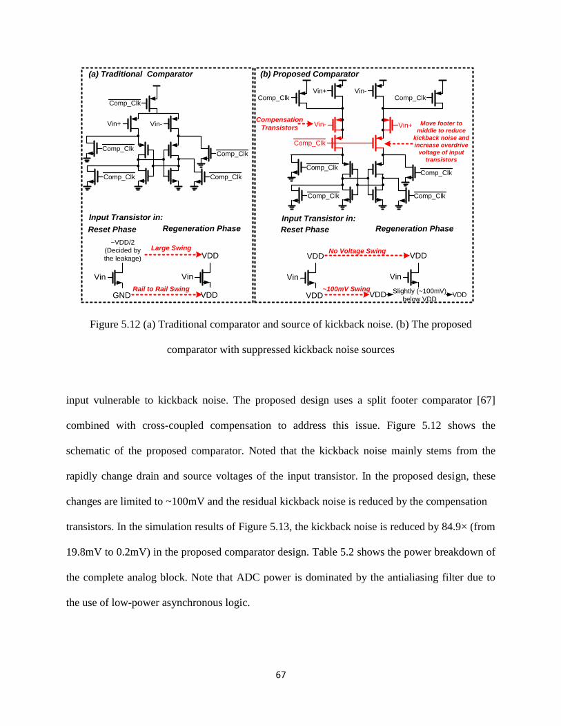
67
Vin+ Vin-
Comp_Clk
Comp_Clk Comp_Clk
Comp_Clk Comp_Clk
Move footer to
middle to reduce
kickback noise and
increase overdrive
voltage of input
transistors
Comp_ClkComp_Clk
(b) Proposed Comparator
Vin+ Vin-
Comp_Clk
Comp_Clk Comp_Clk
Comp_ClkComp_Clk
(a) Traditional Comparator
Vin- Vin+
Reset Phase Regeneration Phase
~VDD/2
(Decided by
the leakage)
Vin
GND
Reset Phase Regeneration Phase
VDD
Vin
VDD
Input Transistor in: Input Transistor in:
VDD
Vin
VDD
VDD
Vin
VDD
No Voltage Swing
~100mV Swing Slightly (~100mV)
below VDDVDD
Rail to Rail Swing
Large Swing
Compensation
Transistors
Figure 5.12 (a) Traditional comparator and source of kickback noise. (b) The proposed
comparator with suppressed kickback noise sources
input vulnerable to kickback noise. The proposed design uses a split footer comparator [67]
combined with cross-coupled compensation to address this issue. Figure 5.12 shows the
schematic of the proposed comparator. Noted that the kickback noise mainly stems from the
rapidly change drain and source voltages of the input transistor. In the proposed design, these
changes are limited to ~100mV and the residual kickback noise is reduced by the compensation
transistors. In the simulation results of Figure 5.13, the kickback noise is reduced by 84.9× (from
19.8mV to 0.2mV) in the proposed comparator design. Table 5.2 shows the power breakdown of
the complete analog block. Note that ADC power is dominated by the antialiasing filter due to
the use of low-power asynchronous logic.

68
0.0 200.0? 400.0?
0.26
0.28
0.30
0.32
0.34
0.26
0.28
0.30
0.32
0.34
0.0
0.2
0.4
0.6
0.80.0
0.2
0.4
0.6
0.80.0
0.2
0.4
0.6
0.8
Time (s)
Proposed Comparator Vin
Traditional Comparator Vin
VOUT+
VOUT-
Vo
lta
ge
(V
)
CLK_B
200.0μ 400.0μ
Figure 5.13 Simulated waveforms of kickback noise in the proposed and traditional comparators.
Kickback noise in the traditional amplifier is 19.8mV and is reduced to 0.2mV in the proposed
design
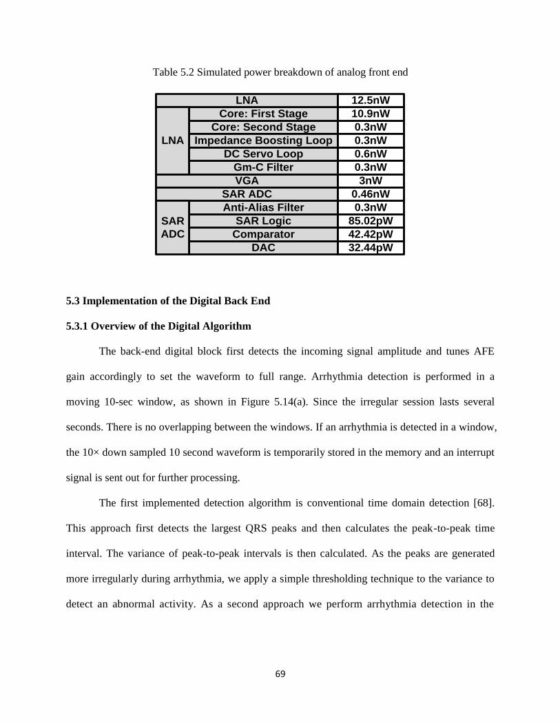
69
Table 5.2 Simulated power breakdown of analog front end
Core: Second Stage
Impedance Boosting Loop
VGA
DAC
0.3nW
0.3nW
0.6nW
3nW
32.44pW
Core: First Stage 10.9nW
Anti-Alias Filter 0.3nW
Comparator 42.42pW
Gm-C Filter 0.3nW
LNA 12.5nW
SAR ADC 0.46nW
SAR Logic 85.02pW
LNA
DC Servo Loop
SAR
ADC
5.3 Implementation of the Digital Back End
5.3.1 Overview of the Digital Algorithm
The back-end digital block first detects the incoming signal amplitude and tunes AFE
gain accordingly to set the waveform to full range. Arrhythmia detection is performed in a
moving 10-sec window, as shown in Figure 5.14(a). Since the irregular session lasts several
seconds. There is no overlapping between the windows. If an arrhythmia is detected in a window,
the 10× down sampled 10 second waveform is temporarily stored in the memory and an interrupt
signal is sent out for further processing.
The first implemented detection algorithm is conventional time domain detection [68].
This approach first detects the largest QRS peaks and then calculates the peak-to-peak time
interval. The variance of peak-to-peak intervals is then calculated. As the peaks are generated
more irregularly during arrhythmia, we apply a simple thresholding technique to the variance to
detect an abnormal activity. As a second approach we perform arrhythmia detection in the
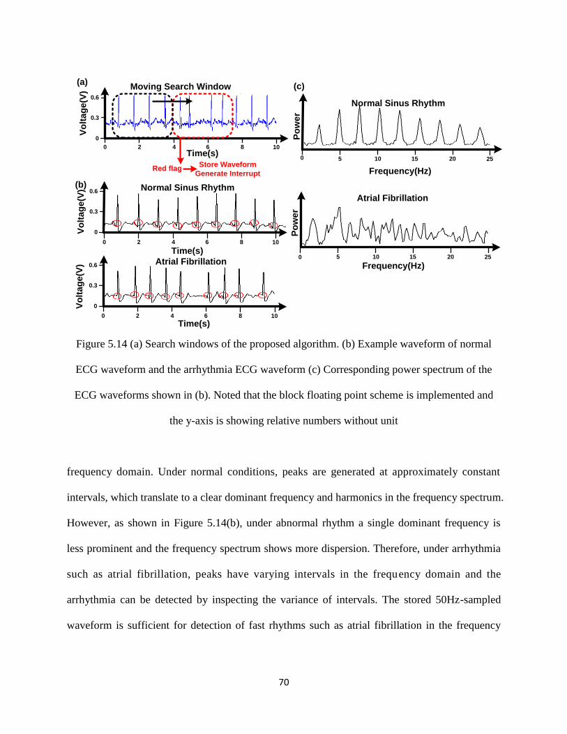
70
Red flag
Time(s)
Moving Search Window
Store Waveform
Generate Interrupt
(a)
Normal Sinus Rhythm
Frequency(Hz)
(c)
Time(s)
(b) Normal Sinus Rhythm
Time(s)
Atrial Fibrillation
Vo
lta
ge(V
)V
olt
ag
e(V
)
0.6
0
0.3
0.6
0
0.3
0.6
0
0.3
100 2 4 6 8
100 2 4 6 8
100 2 4 6 8
Vo
lta
ge(V
)
255 10 15 200
Po
we
r
Frequency(Hz)255 10 15 20
Po
we
r
Atrial Fibrillation
0
Figure 5.14 (a) Search windows of the proposed algorithm. (b) Example waveform of normal
ECG waveform and the arrhythmia ECG waveform (c) Corresponding power spectrum of the
ECG waveforms shown in (b). Noted that the block floating point scheme is implemented and
the y-axis is showing relative numbers without unit
frequency domain. Under normal conditions, peaks are generated at approximately constant
intervals, which translate to a clear dominant frequency and harmonics in the frequency spectrum.
However, as shown in Figure 5.14(b), under abnormal rhythm a single dominant frequency is
less prominent and the frequency spectrum shows more dispersion. Therefore, under arrhythmia
such as atrial fibrillation, peaks have varying intervals in the frequency domain and the
arrhythmia can be detected by inspecting the variance of intervals. The stored 50Hz-sampled
waveform is sufficient for detection of fast rhythms such as atrial fibrillation in the frequency
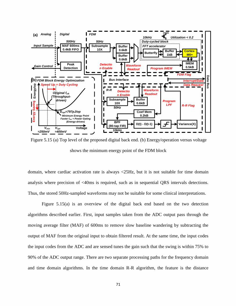
71
MAF 600ms
0.4kB FIFO
Analog Digital
500Hz
Gain Control
50Hz
Utilization < 0.2
10kHz
R-R
Bus Interface
50Hz
10kHz
Waveform
Readout
Peak
Detection
Subsample
10XBuffer
0.6kB
Buffer
0.6kB
ButterflyBuffer
1kB
Cortex-
M0+
Duty-cycled block
FFT accelerator
IMEM
0.5kB
Detectio
n Enable
Buffer
0.6kB
Detectio
n Enable
Subsample
10X
Program IMEM
Waveform
Readout
Coef Mem
0.2kB
Program
LPF
BPF
(80-tap FIR)D(t) - D(t-1) Variance(X)
Input Sample
Da
ta B
us
Interrupt/Data
Data Request
R-R Flag
FDM Flag
FDM
Minimum Energy Point
Faster fclk + Power Gating
(Energy-driven)
En
erg
y/o
p
Original fclk
(Throughput-
driven)
Vmin
Speed Up + Duty Cycling
FDM Block Energy Optimization
VoltageVopt
En
erg
y S
av
ing
(a)
(b)
=250mV =400mV
Eopt=797pJ/op
Figure 5.15 (a) Top level of the proposed digital back end. (b) Energy/operation versus voltage
shows the minimum energy point of the FDM block
domain, where cardiac activation rate is always <25Hz, but it is not suitable for time domain
analysis where precision of <40ms is required, such as in sequential QRS intervals detections.
Thus, the stored 50Hz-sampled waveforms may not be suitable for some clinical interpretations.
Figure 5.15(a) is an overview of the digital back end based on the two detection
algorithms described earlier. First, input samples taken from the ADC output pass through the
moving average filter (MAF) of 600ms to remove slow baseline wandering by subtracting the
output of MAF from the original input to obtain filtered result. At the same time, the input codes
the input codes from the ADC and are sensed tunes the gain such that the swing is within 75% to
90% of the ADC output range. There are two separate processing paths for the frequency domain
and time domain algorithms. In the time domain R-R algorithm, the feature is the distance
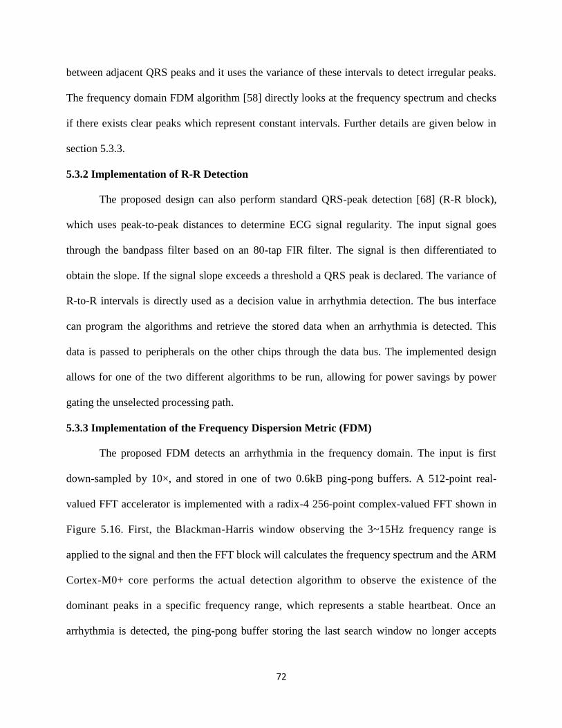
72
between adjacent QRS peaks and it uses the variance of these intervals to detect irregular peaks.
The frequency domain FDM algorithm [58] directly looks at the frequency spectrum and checks
if there exists clear peaks which represent constant intervals. Further details are given below in
section 5.3.3.
5.3.2 Implementation of R-R Detection
The proposed design can also perform standard QRS-peak detection [68] (R-R block),
which uses peak-to-peak distances to determine ECG signal regularity. The input signal goes
through the bandpass filter based on an 80-tap FIR filter. The signal is then differentiated to
obtain the slope. If the signal slope exceeds a threshold a QRS peak is declared. The variance of
R-to-R intervals is directly used as a decision value in arrhythmia detection. The bus interface
can program the algorithms and retrieve the stored data when an arrhythmia is detected. This
data is passed to peripherals on the other chips through the data bus. The implemented design
allows for one of the two different algorithms to be run, allowing for power savings by power
gating the unselected processing path.
5.3.3 Implementation of the Frequency Dispersion Metric (FDM)
The proposed FDM detects an arrhythmia in the frequency domain. The input is first
down-sampled by 10×, and stored in one of two 0.6kB ping-pong buffers. A 512-point real-
valued FFT accelerator is implemented with a radix-4 256-point complex-valued FFT shown in
Figure 5.16. First, the Blackman-Harris window observing the 3~15Hz frequency range is
applied to the signal and then the FFT block will calculates the frequency spectrum and the ARM
Cortex-M0+ core performs the actual detection algorithm to observe the existence of the
dominant peaks in a specific frequency range, which represents a stable heartbeat. Once an
arrhythmia is detected, the ping-pong buffer storing the last search window no longer accepts
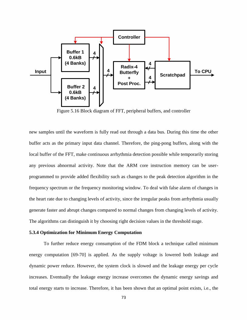
73
Buffer 1
0.6kB
(4 Banks)Radix-4
Butterfly
+
Post Proc. Buffer 2
0.6kB
(4 Banks)
4
4
4Scratchpad
Input
4
4
To CPU
Controller
Figure 5.16 Block diagram of FFT, peripheral buffers, and controller
new samples until the waveform is fully read out through a data bus. During this time the other
buffer acts as the primary input data channel. Therefore, the ping-pong buffers, along with the
local buffer of the FFT, make continuous arrhythmia detection possible while temporarily storing
any previous abnormal activity. Note that the ARM core instruction memory can be user-
programmed to provide added flexibility such as changes to the peak detection algorithm in the
frequency spectrum or the frequency monitoring window. To deal with false alarm of changes in
the heart rate due to changing levels of activity, since the irregular peaks from arrhythmia usually
generate faster and abrupt changes compared to normal changes from changing levels of activity.
The algorithms can distinguish it by choosing right decision values in the threshold stage.
5.3.4 Optimization for Minimum Energy Computation
To further reduce energy consumption of the FDM block a technique called minimum
energy computation [69-70] is applied. As the supply voltage is lowered both leakage and
dynamic power reduce. However, the system clock is slowed and the leakage energy per cycle
increases. Eventually the leakage energy increase overcomes the dynamic energy savings and
total energy starts to increase. Therefore, it has been shown that an optimal point exists, i.e., the
74
minimum point of the plot in Figure 5.15(b). In simulation, Vopt and Vmin are 300mV and
250mV whereas we could achieve the same performance as Vopt in simulation at 400mV in
measurement due to discrepancy between simulation and measurement. And the energy per
operation is 797pJ/op at Vopt. Arrhythmia detection is done only once in a 10-sec window and
each detection takes approximately 500 cycles. Hence, 500Hz input sampling frequency is
sufficient to meet performance constraints and is chosen for the proposed system. However, the
minimum supply voltage that matches this frequency constraint lies below the energy optimal
point and therefore consumes substantial leakage energy due to the corresponding long cycle
time. Therefore, we use a faster (10kHz) clock and operate the detection in burst-mode (20×
faster than required). After the detection event completes the entire block, including the FFT and
M0+ core, is power gated with an NMOS header using a boosted enable signal. Although a
higher operating voltage is needed for this faster clock frequency, the leakage energy per
computation is greatly reduced and minimum possible energy consumption is achieved.
Compared to the supply voltage corresponding to just-in-time computation, this
technique increases supply voltage by 50mV while reducing energy by 40%.
5.4. Measurement Results
5.4.1 Proposed AFE Measured Results
Figure 5.17 (a) is the chip microphotograph of the proposed SoC and the Figure 5.17 (b)
shows the chip inside the syringe needle. It is fabricated in 65nm LP CMOS technology. The
amplifier achieves 2.64 NEF with 31nA current consumption and 6.52µV input referred root
mean square noise. The measured amplifier gain ranges from 51 to 96dB with 250Hz bandwidth.
The frequency response of the amplifier is shown in Fig. 18. The amplifier CMRR and PSRR are
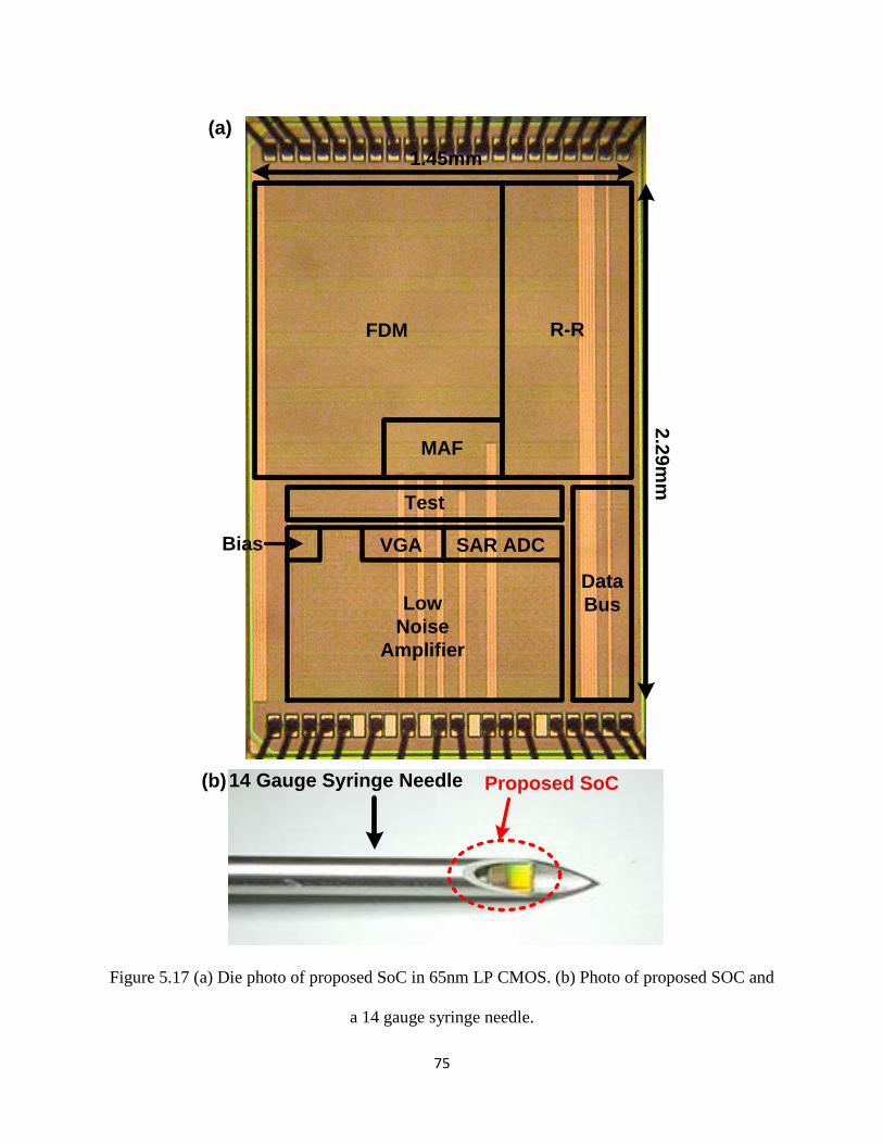
75
SAR ADC
Low
Noise
Amplifier
VGABias
Test
Data
Bus
FDM
MAF
R-R
1.45mm
2.2
9m
m
14 Gauge Syringe Needle Proposed SoC(b)
(a)
Figure 5.17 (a) Die photo of proposed SoC in 65nm LP CMOS. (b) Photo of proposed SOC and
a 14 gauge syringe needle.
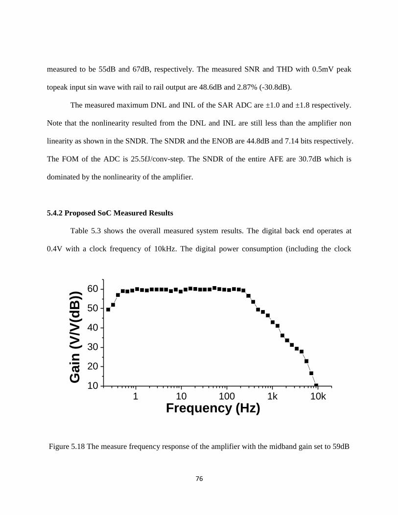
76
measured to be 55dB and 67dB, respectively. The measured SNR and THD with 0.5mV peak
topeak input sin wave with rail to rail output are 48.6dB and 2.87% (-30.8dB).
The measured maximum DNL and INL of the SAR ADC are ±1.0 and ±1.8 respectively.
Note that the nonlinearity resulted from the DNL and INL are still less than the amplifier non
linearity as shown in the SNDR. The SNDR and the ENOB are 44.8dB and 7.14 bits respectively.
The FOM of the ADC is 25.5fJ/conv-step. The SNDR of the entire AFE are 30.7dB which is
dominated by the nonlinearity of the amplifier.
5.4.2 Proposed SoC Measured Results
Table 5.3 shows the overall measured system results. The digital back end operates at
0.4V with a clock frequency of 10kHz. The digital power consumption (including the clock
1 10 100 1k 10k10
20
30
40
50
60
Ga
in (
V/V
(dB
))
Frequency (Hz)
Figure 5.18 The measure frequency response of the amplifier with the midband gain set to 59dB
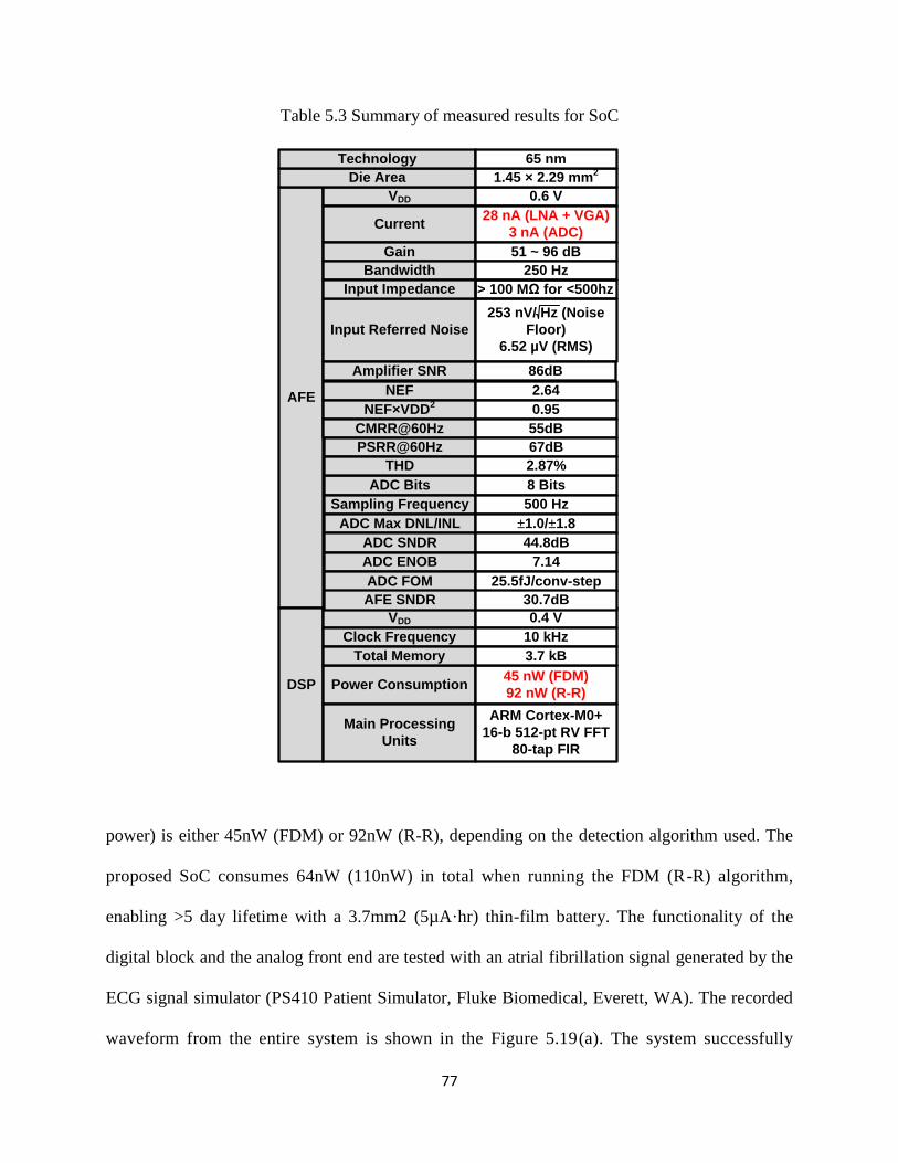
77
Table 5.3 Summary of measured results for SoC
> 100 MΩ for <500hz
AFE
VDD
Current
Gain
Bandwidth
Input Referred Noise
ADC Bits
Sampling Frequency
DSP
VDD
Power Consumption
Clock Frequency
0.6 V
28 nA (LNA + VGA)
3 nA (ADC)
51 ~ 96 dB
250 Hz
253 nV/ Hz (Noise
Floor)
6.52 µV (RMS)
8 Bits
500 Hz
0.4 V
10 kHz
45 nW (FDM)
92 nW (R-R)
Die Area 1.45 × 2.29 mm2
NEF 2.64
NEF×VDD2
0.95
Input Impedance
Total Memory 3.7 kB
Technology 65 nm
Main Processing
Units
ARM Cortex-M0+
16-b 512-pt RV FFT
80-tap FIR
CMRR@60Hz 55dB
PSRR@60Hz 67dB
THD 2.87%
Amplifier SNR 86dB
ADC Max DNL/INL
ADC SNDR
±1.0/±1.8
44.8dB
ADC ENOB 7.14
ADC FOM 25.5fJ/conv-step
AFE SNDR 30.7dB
power) is either 45nW (FDM) or 92nW (R-R), depending on the detection algorithm used. The
proposed SoC consumes 64nW (110nW) in total when running the FDM (R-R) algorithm,
enabling >5 day lifetime with a 3.7mm2 (5µA·hr) thin-film battery. The functionality of the
digital block and the analog front end are tested with an atrial fibrillation signal generated by the
ECG signal simulator (PS410 Patient Simulator, Fluke Biomedical, Everett, WA). The recorded
waveform from the entire system is shown in the Figure 5.19(a). The system successfully
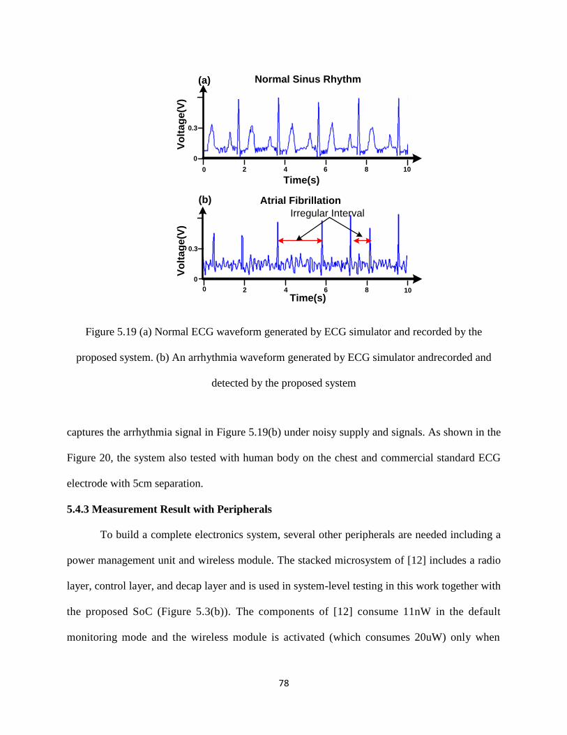
78
Normal Sinus Rhythm
Atrial Fibrillation
(a)
(b)
Irregular Interval
Time(s)2 4 6 80
Time(s)2 4 6 80 10
10
Vo
lta
ge
(V)
0
0.3
0
0.3
Vo
lta
ge(V
)
Figure 5.19 (a) Normal ECG waveform generated by ECG simulator and recorded by the
proposed system. (b) An arrhythmia waveform generated by ECG simulator andrecorded and
detected by the proposed system
captures the arrhythmia signal in Figure 5.19(b) under noisy supply and signals. As shown in the
Figure 20, the system also tested with human body on the chest and commercial standard ECG
electrode with 5cm separation.
5.4.3 Measurement Result with Peripherals
To build a complete electronics system, several other peripherals are needed including a
power management unit and wireless module. The stacked microsystem of [12] includes a radio
layer, control layer, and decap layer and is used in system-level testing in this work together with
the proposed SoC (Figure 5.3(b)). The components of [12] consume 11nW in the default
monitoring mode and the wireless module is activated (which consumes 20uW) only when
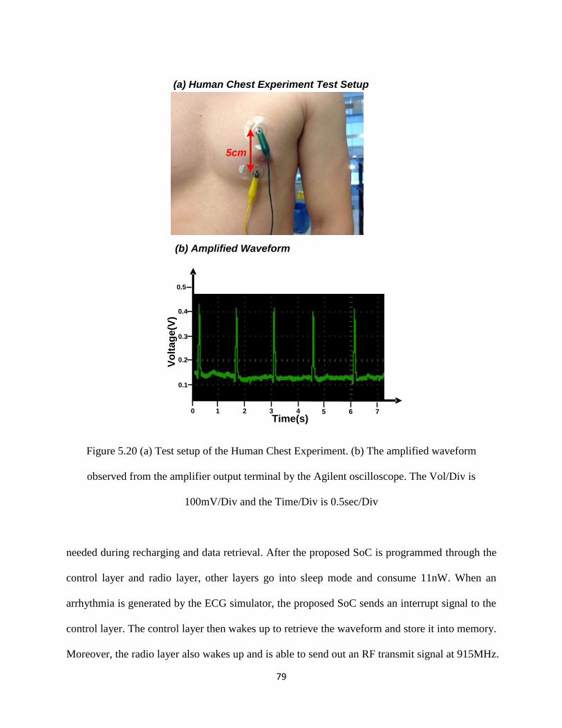
79
5cm
(a) Human Chest Experiment Test Setup
(b) Amplified Waveform
0.4
0.3
Vo
lta
ge(V
)
0.2
0.1
0.5
Time(s)1 2 3 4 5 6 70
Figure 5.20 (a) Test setup of the Human Chest Experiment. (b) The amplified waveform
observed from the amplifier output terminal by the Agilent oscilloscope. The Vol/Div is
100mV/Div and the Time/Div is 0.5sec/Div
needed during recharging and data retrieval. After the proposed SoC is programmed through the
control layer and radio layer, other layers go into sleep mode and consume 11nW. When an
arrhythmia is generated by the ECG simulator, the proposed SoC sends an interrupt signal to the
control layer. The control layer then wakes up to retrieve the waveform and store it into memory.
Moreover, the radio layer also wakes up and is able to send out an RF transmit signal at 915MHz.
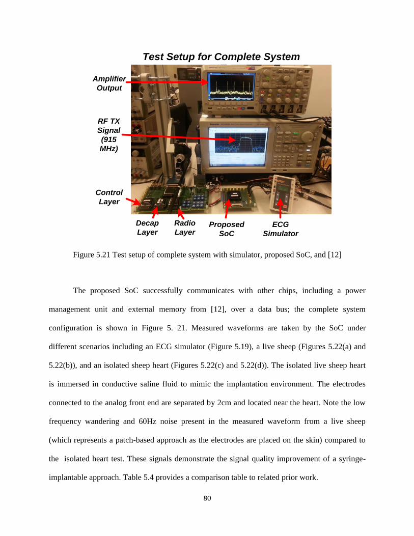
80
ECG
Simulator
Proposed
SoC
RF TX
Signal
(915
MHz)
Decap
Layer
Amplifier
Output
Test Setup for Complete System
Radio
Layer
Control
Layer
Figure 5.21 Test setup of complete system with simulator, proposed SoC, and [12]
The proposed SoC successfully communicates with other chips, including a power
management unit and external memory from [12], over a data bus; the complete system
configuration is shown in Figure 5. 21. Measured waveforms are taken by the SoC under
different scenarios including an ECG simulator (Figure 5.19), a live sheep (Figures 5.22(a) and
5.22(b)), and an isolated sheep heart (Figures 5.22(c) and 5.22(d)). The isolated live sheep heart
is immersed in conductive saline fluid to mimic the implantation environment. The electrodes
connected to the analog front end are separated by 2cm and located near the heart. Note the low
frequency wandering and 60Hz noise present in the measured waveform from a live sheep
(which represents a patch-based approach as the electrodes are placed on the skin) compared to
the isolated heart test. These signals demonstrate the signal quality improvement of a syringe-
implantable approach. Table 5.4 provides a comparison table to related prior work.
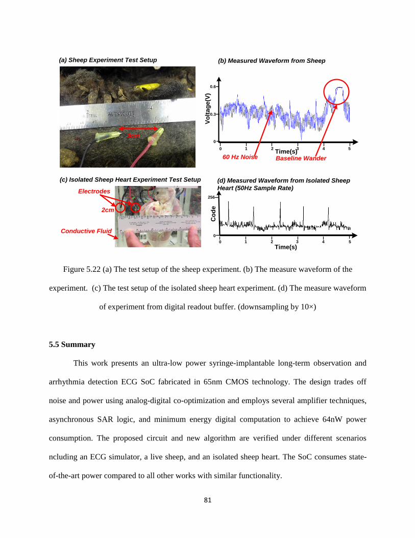
81
(a) Sheep Experiment Test Setup
3cm
Baseline Wander60 Hz Noise
(b) Measured Waveform from Sheep
Time(s)
(c) Isolated Sheep Heart Experiment Test Setup
Electrodes
2cm
Conductive Fluid
(d) Measured Waveform from Isolated Sheep
Heart (50Hz Sample Rate)
Time(s)
1 2 3 40 5
0.6
0
0.3
Vo
lta
ge
(V)
1 2 3 40 5
0
256
Co
de
Figure 5.22 (a) The test setup of the sheep experiment. (b) The measure waveform of the
experiment. (c) The test setup of the isolated sheep heart experiment. (d) The measure waveform
of experiment from digital readout buffer. (downsampling by 10×)
5.5 Summary
This work presents an ultra-low power syringe-implantable long-term observation and
arrhythmia detection ECG SoC fabricated in 65nm CMOS technology. The design trades off
noise and power using analog-digital co-optimization and employs several amplifier techniques,
asynchronous SAR logic, and minimum energy digital computation to achieve 64nW power
consumption. The proposed circuit and new algorithm are verified under different scenarios
ncluding an ECG simulator, a live sheep, and an isolated sheep heart. The SoC consumes state-
of-the-art power compared to all other works with similar functionality.
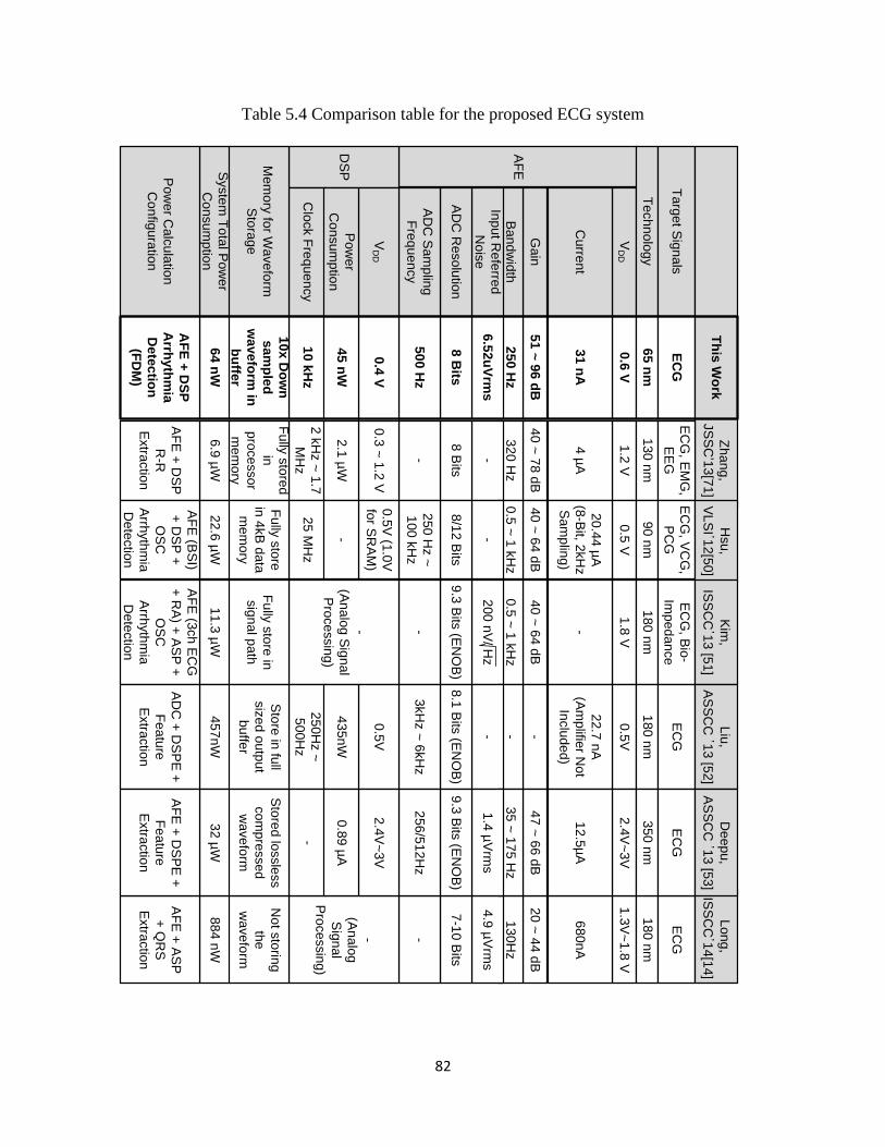
82
Table 5.4 Comparison table for the proposed ECG system
Zh
an
g,
JS
SC’1
3[7
1]
AF
E
VD
D
Cu
rren
t
Ga
in
Ba
nd
wid
thIn
pu
t Re
ferre
d
No
ise
AD
C R
eso
lutio
n
AD
C S
am
plin
g
Fre
qu
en
cy
DS
P
VD
D
Clo
ck F
req
ue
ncy
0.6
V
31
nA
51
~ 9
6 d
B
25
0 H
z
6.5
2u
Vrm
s
8 B
its
50
0 H
z
0.4
V
10
kH
z
45
nW
Te
ch
no
log
y6
5 n
m
Syste
m T
ota
l Po
we
r
Co
nsu
mp
tion
Po
we
r Ca
lcu
latio
n
Co
nfig
ura
tion
Ta
rge
t Sig
na
lsE
CG
64
nW
AF
E +
DS
P
Arrh
yth
mia
De
tec
tion
(FD
M)
Th
is W
ork
1.2
V
4 µ
A
40
~ 7
8 d
B
32
0 H
z
-
8 B
its
-
0.3
~ 1
.2 V
2 k
Hz ~
1.7
MH
z
2.1
µW
13
0 n
m
EC
G, E
MG
,
EE
G
6.9
µW
AF
E +
DS
P
R-R
Extra
ctio
n
0.5
V
20
.44
µA
(8-B
it, 2kH
z
Sa
mp
ling
)
40
~ 6
4 d
B
0.5
~ 1
kH
z
-
8/1
2 B
its
25
0 H
z ~
10
0 k
Hz
0.5
V (1
.0V
for S
RA
M)
25
MH
z
-
90
nm
EC
G, V
CG
,
PC
G
22.6
µW
AF
E (B
SI)
+ D
SP
+
OS
C
Arrh
yth
mia
De
tectio
n
Hsu
,
VL
SI’1
2[5
0]
1.8
V
-
40
~ 6
4 d
B
0.5
~ 1
kH
z
20
0 n
V/ H
z
9.3
Bits
(EN
OB
)
--
(An
alo
g S
ign
al
Pro
ce
ssin
g)
18
0 n
m
EC
G, B
io-
Imp
ed
an
ce
11
.3 µ
W
AF
E (3
ch
EC
G
+ R
A) +
AS
P +
OS
C
Arrh
yth
mia
De
tectio
n
Kim
,
ISS
CC’1
3 [5
1]
1.3
V~
1.8
V
68
0n
A
20
~ 4
4 d
B
13
0H
z
4.9
µV
rms
7-1
0 B
its
--
(An
alo
g
Sig
na
l
Pro
ce
ssin
g)
18
0 n
m
EC
G
88
4 n
W
AF
E +
AS
P
+ Q
RS
Extra
ctio
n
Lo
ng
,
ISS
CC’1
4[1
4]
0.5
V
22.7
nA
(Am
plifie
r No
t
Inclu
de
d)
---
8.1
Bits
(EN
OB
)
3kH
z ~
6kH
z
18
0 n
m
EC
G
45
7n
W
AD
C +
DS
PE
+
Fe
atu
re
Extra
ctio
n
Liu
,
AS
SC
C ’1
3 [5
2]
0.5
V
25
0H
z ~
50
0H
z
43
5n
W
2.4
V~
3V
12.5
µA
47
~ 6
6 d
B
35
~ 1
75
Hz
1.4
µV
rms
9.3
Bits
(EN
OB
)
25
6/5
12
Hz
35
0 n
m
EC
G
32
µW
AF
E +
DS
PE
+
Fe
atu
re
Extra
ctio
n
De
ep
u,
AS
SC
C ’1
3 [5
3]
2.4
V~
3V
-
0.8
9 µ
AP
ow
er
Co
nsu
mp
tion
Me
mo
ry fo
r Wa
ve
form
Sto
rag
e
10
x D
ow
n
sa
mp
led
wa
ve
form
in
bu
ffer
Fu
lly s
tore
d
in
pro
ce
sso
r
me
mo
ry
Fu
lly s
tore
in 4
kB
da
ta
me
mo
ry
Fu
lly s
tore
in
sig
na
l pa
th
No
t sto
ring
the
wa
ve
form
Sto
re in
full
siz
ed
ou
tpu
t
bu
ffer
Sto
red
lossle
ss
co
mp
resse
d
wa
ve
form

83
CHAPTER 6
Conclusion
6.1 Conclusion
Since the invention of the transistors and the integrated circuits, the continuous
development on scaling for decades have resulted in smaller and smaller electronics devices
surrounding the world. Nowadays, the mainstream devices have been changed from the desktop
computers and laptops to the tablets and cellphones. And eventually technological advances
might lead the next generation computer to minature sensor nodes for the internet of things (IoT).
There are many challenges have raised for the small form factor minature sensor nodes.
The most critical one is the low power requirement since the limits form the small battery
capacity directly caused by the severe physical size constraints on the battery. As a result, better
power efficiency and power saving techniques is required to allow these systems to operate
under extreme low power budget. In such systems the better power efficiency of the digital
blocks can usually achieved by the benefit of the scaling. However, the power efficiency of the
analog part is limited by the fundamental requirement of the signal to noise ratio (SNR) and
become a key issue for low power design. To address this issue, in this dissertation, several new
techniques are introduced and discussed to reduce the power consumption and improve the
efficiency to achieve longer lifetime for the entire systems.
84
The power consumption can usually be written as follows:
𝑇𝑜𝑡𝑎𝑙 𝑃𝑜𝑤𝑒𝑟 = 𝐴𝑐𝑡𝑖𝑣𝑒 𝑅𝑎𝑡𝑒 × 𝐴𝑐𝑡𝑖𝑣𝑒 𝑃𝑜𝑤𝑒𝑟 + 𝑆𝑙𝑒𝑒𝑝 𝑃𝑜𝑤𝑒𝑟 … … … … … … … … … … … . (6.1)
Each chapter in this dissertation has a focus on the equation. In chapter 2, a sample and
hold bandgap voltage reference is presented. The main focus of the design on the bandgap
voltage reference design is on reducing the “active rate” of the block. In order to decrease the
active rate, the fast turn-on technique is used to reduce the wakeup time by 11.5× (from 55ms to
4.8ms) while the low leakage switch (decrease the leakage by more than 1000×) and the gate
leakage compensator (decrease the leakage by 2.75× after low leakage switch) is used to
lengthen the sleep time. And self-timing canary circuits is used to control the time period. As a
results, the proposed marks 251× power improvement over the best prior bandgap voltage
reference and is still 9.73× less power than the voltage reference published in 2015[84,85].
In chapter 3, an ultralow-leakage electrostatic discharge (ESD) power clamp designs for
wireless sensor applications are proposed and implemented in 0.18μm CMOS is presented. The
design is emphasis on reducing the leakage which is the “sleep power’ of the entire systems in
the sleep mode since the ESD is required to be always-on for the system protection. By applying
porper choice of device size the capacitor, double stacking (2.9× leakage reduction) and GIDL
reduction (5.4× more leakage reduction after double stacking)the overall leakage is reduced by
139×.
In chapter 4, a low power high efficiency neural signal recording amplifier is presented.
The major improvement of it is developing a novel multi-chopper technique to establish the
trade-off between the bandwidth and noise and break the fundamental limit of the power
consumption due to the SNR requirement. Hence it is on reducing the “active power”. The input
85
referred root mean square noise is 1.54μV (1-500Hz) with 266nA tail current corresponding to a
1.38 noise efficiency factor, which is the best reported among current state-of-the-art amplifiers.
Finally, in chapter 5, a system level design on syringe-implantable electrocardiography
(ECG) monitoring system is proposed which is beyond the scope of the equation. The co-
optimize power consumption with digital building blocks and the circuit techniques in the analog
front end (AFE) enable 31nA current consumption. The proposed SoC is fabricated in 65nm
CMOS and consumes 64nW while successfully detecting atrial fibrillation arrhythmia and
storing the irregular waveform in memory in experiments using an ECG simulator, a live sheep,
and an isolated sheep heart.
The aforementioned low power techniques in this dissertation can be generally used to
overcome the low power design challenge and extend the system lifetime.
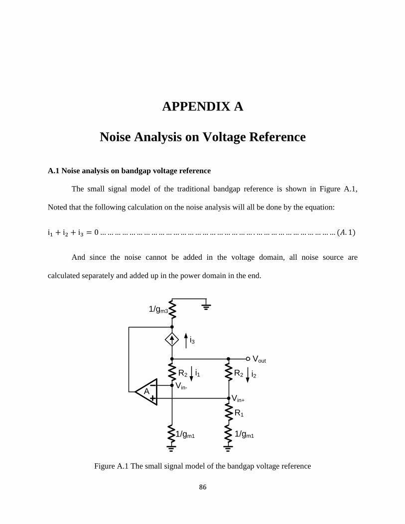
86
APPENDIX A
Noise Analysis on Voltage Reference
A.1 Noise analysis on bandgap voltage reference
The small signal model of the traditional bandgap reference is shown in Figure A.1,
Noted that the following calculation on the noise analysis will all be done by the equation:
i1 + i2 + i3 = 0 … … … … … … … … … … … … … … … … … … … … … . … … … … … … … … … … … (𝐴. 1)
And since the noise cannot be added in the voltage domain, all noise source are
calculated separately and added up in the power domain in the end.
R2 R2
R1
A
1/gm3
1/gm11/gm1
i1 i2
i3
Vin+
Vin-
Vout
Figure A.1 The small signal model of the bandgap voltage reference
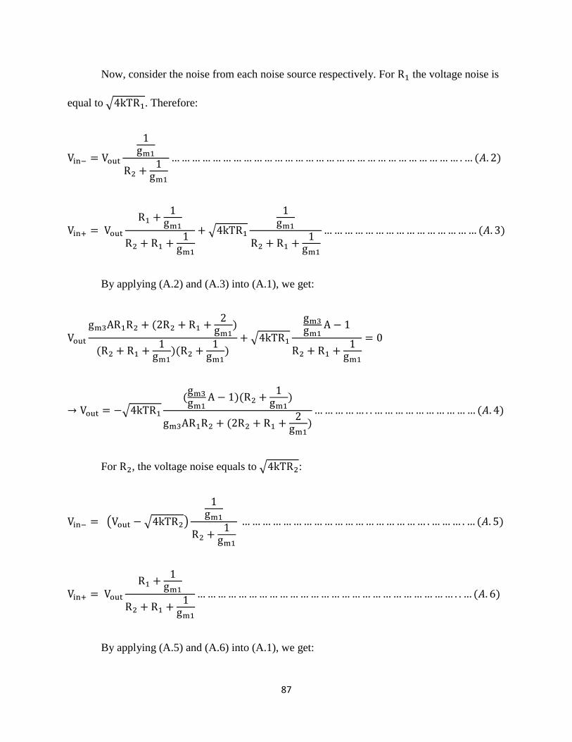
87
Now, consider the noise from each noise source respectively. For R1 the voltage noise is
equal to √4kTR1. Therefore:
Vin− = Vout
1gm1
R2 +1
gm1
… … … … … … … … … … … … … … … … … … … … … … … … … … … … . … (𝐴. 2)
Vin+ = Vout
R1 +1
gm1
R2 + R1 +1
gm1
+ √4kTR1
1gm1
R2 + R1 +1
gm1
… … … … … … … … … … … … … … … (𝐴. 3)
By applying (A.2) and (A.3) into (A.1), we get:
Vout
gm3AR1R2 + (2R2 + R1 +2
gm1)
(R2 + R1 +1
gm1)(R2 +
1gm1
)+ √4kTR1
gm3
gm1A − 1
R2 + R1 +1
gm1
= 0
→ Vout = −√4kTR1
(gm3
gm1A − 1)(R2 +
1gm1
)
gm3AR1R2 + (2R2 + R1 +2
gm1)
… … … … … . . … … … … … … … … … … (𝐴. 4)
For R2, the voltage noise equals to √4kTR2:
Vin− = (Vout − √4kTR2)
1gm1
R2 +1
gm1
… … … … … … … … … … … … … … … … … … . … … … . … (𝐴. 5)
Vin+ = Vout
R1 +1
gm1
R2 + R1 +1
gm1
… … … … … … … … … … … … … … … … … … … … … … … … … . . … (𝐴. 6)
By applying (A.5) and (A.6) into (A.1), we get:
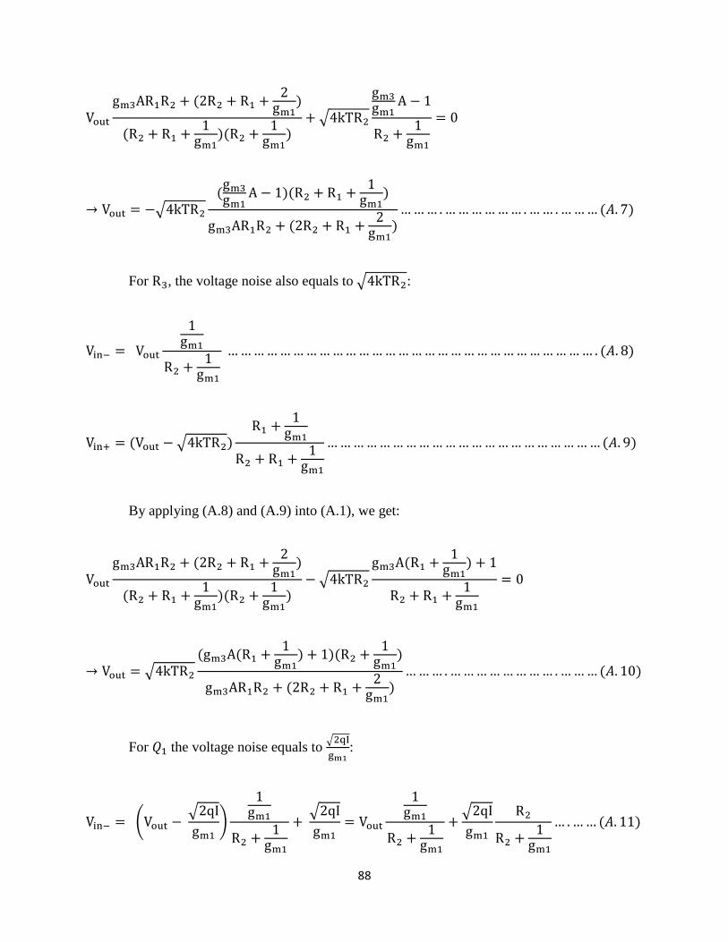
88
Vout
gm3AR1R2 + (2R2 + R1 +2
gm1)
(R2 + R1 +1
gm1)(R2 +
1gm1
)+ √4kTR2
gm3
gm1A − 1
R2 +1
gm1
= 0
→ Vout = −√4kTR2
(gm3
gm1A − 1)(R2 + R1 +
1gm1
)
gm3AR1R2 + (2R2 + R1 +2
gm1)
… … … . … … … … … … . … … . … … … (𝐴. 7)
For R3, the voltage noise also equals to √4kTR2:
Vin− = Vout
1gm1
R2 +1
gm1
… … … … … … … … … … … … … … … … … … … … … … … … … … … … . (𝐴. 8)
Vin+ = (Vout − √4kTR2)R1 +
1gm1
R2 + R1 +1
gm1
… … … … … … … … … … … … … … … … … … … … … (𝐴. 9)
By applying (A.8) and (A.9) into (A.1), we get:
Vout
gm3AR1R2 + (2R2 + R1 +2
gm1)
(R2 + R1 +1
gm1)(R2 +
1gm1
)− √4kTR2
gm3A(R1 +1
gm1) + 1
R2 + R1 +1
gm1
= 0
→ Vout = √4kTR2
(gm3A(R1 +1
gm1) + 1)(R2 +
1gm1
)
gm3AR1R2 + (2R2 + R1 +2
gm1)
… … … . … … … … … … … … . … … … (𝐴. 10)
For 𝑄1 the voltage noise equals to √2qI
gm1:
Vin− = (Vout − √2qI
gm1)
1gm1
R2 +1
gm1
+ √2qI
gm1= Vout
1gm1
R2 +1
gm1
+√2qI
gm1
R2
R2 +1
gm1
… . … … (𝐴. 11)
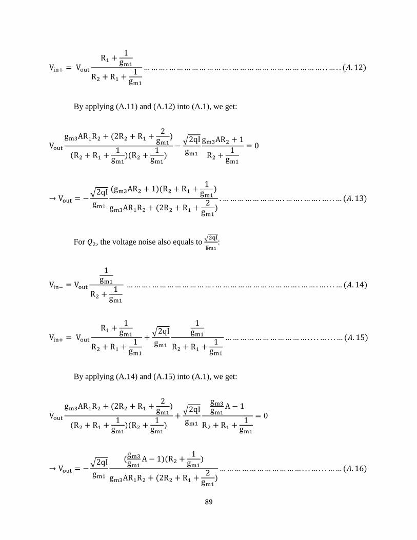
89
Vin+ = Vout
R1 +1
gm1
R2 + R1 +1
gm1
… … … . … … … … … … … … . … … … … … … … … … … … … . . … . . (𝐴. 12)
By applying (A.11) and (A.12) into (A.1), we get:
Vout
gm3AR1R2 + (2R2 + R1 +2
gm1)
(R2 + R1 +1
gm1)(R2 +
1gm1
)−
√2qI
gm1
gm3AR2 + 1
R2 +1
gm1
= 0
→ Vout = −√2qI
gm1
(gm3AR2 + 1)(R2 + R1 +1
gm1)
gm3AR1R2 + (2R2 + R1 +2
gm1)
. … … … … … … … … . … … . … … . … . . … (𝐴. 13)
For 𝑄2, the voltage noise also equals to √2qI
gm1:
Vin− = Vout
1gm1
R2 +1
gm1
… … … . … … … … … … … … . … … … … … … … … … … … . … … . … . . . … (𝐴. 14)
Vin+ = Vout
R1 +1
gm1
R2 + R1 +1
gm1
+√2qI
gm1
1gm1
R2 + R1 +1
gm1
… … … … … … … … … … … . . . . … . . . … (𝐴. 15)
By applying (A.14) and (A.15) into (A.1), we get:
Vout
gm3AR1R2 + (2R2 + R1 +2
gm1)
(R2 + R1 +1
gm1)(R2 +
1gm1
)+
√2qI
gm1
gm3
gm1A − 1
R2 + R1 +1
gm1
= 0
→ Vout = −√2qI
gm1
(gm3
gm1A − 1)(R2 +
1gm1
)
gm3AR1R2 + (2R2 + R1 +2
gm1)
… … … … … … … … … … … . . . … . . . … … (𝐴. 16)
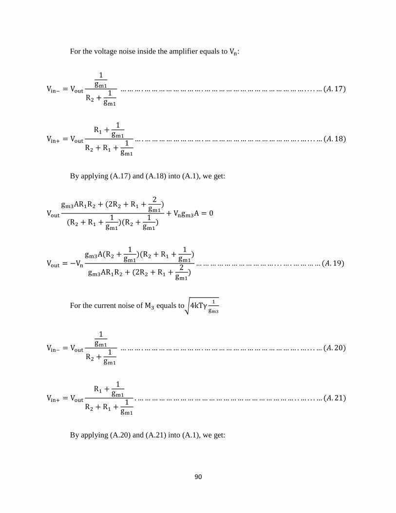
90
For the voltage noise inside the amplifier equals to Vn:
Vin− = Vout
1gm1
R2 +1
gm1
… … … . … … … … … … … … . … … … … … … … … … … … … … … . . . . … (𝐴. 17)
Vin+ = Vout
R1 +1
gm1
R2 + R1 +1
gm1
… . … … … … … … … … . … … … … … … … … … … … … … . … . . . … (𝐴. 18)
By applying (A.17) and (A.18) into (A.1), we get:
Vout
gm3AR1R2 + (2R2 + R1 +2
gm1)
(R2 + R1 +1
gm1)(R2 +
1gm1
)+ Vngm3A = 0
Vout = −Vn
gm3A(R2 +1
gm1)(R2 + R1 +
1gm1
)
gm3AR1R2 + (2R2 + R1 +2
gm1)
… … … … … … … … … … … . . . … . … … … … (𝐴. 19)
For the current noise of M3 equals to√4kTγ1
gm3
Vin− = Vout
1gm1
R2 +1
gm1
… … … . … … … … … … … … . … … … … … … … … … … … … … . … . . . … (𝐴. 20)
Vin+ = Vout
R1 +1
gm1
R2 + R1 +1
gm1
. … … … … … … … … … … … … … … … … … … … … … … . . … . . . … (𝐴. 21)
By applying (A.20) and (A.21) into (A.1), we get:

91
Vout
gm3AR1R2 + (2R2 + R1 +2
gm1)
(R2 + R1 +1
gm1)(R2 +
1gm1
)+ √4kTγgm3 = 0
→ Vout = −√4kTγgm3
(R2 +1
gm1)(R2 + R1 +
1gm1
)
gm3AR1R2 + (2R2 + R1 +2
gm1)
… … … … … … … … … . … … . . . . … (𝐴. 22)
Combine all the noise equations: (A.4), (A.7), (A.10), (A13), (A.16), (A.19) and (A.22)
together by summing all the noise in the power domain. The total noise of the entire reference is:
Vn,total2
=
((4kTR1 +2qIgm1
2 ) (gm3
gm1A − 1)
2
+ 4kTR2 ((gm3A(R1 +1
gm1) + 1)
2
) (gm1R2 + 1)2
(gm1gm3AR1R2 + (2gm1R2 + gm1R1 + 2))2
+
(4kTR2 (gm3
gm1A − 1)
2
+2qIgm1
2 (gm3AR2 + 1)2) (gm1R2 + gm1R1 + 1)2
(gm1gm3AR1R2 + (2gm1R2 + gm1R1 + 2))2
+
(Vn2 gm3
2
gm12 A2 + 4kTγ
gm3
gm12 )(gm1R2 + 1)2(gm1R2 + gm1R1 + 1)2
(gm1gm3AR1R2 + (2gm1R2 + gm1R1 + 2))2
… … … … … . … . . . . . . … (𝐴. 23)

92
ro
1/gm
Vref
ro
1/gm
Vref
ro
1/gm
(a) 2-T voltage reference (b) 4-T voltage reference
I1
I2
Figure A.2 The small signal model of the 2-T and 4-T voltage reference
A.2 Noise analysis on 2-T and 4-T voltage reference
The small signal model of the 2-T and 4-T voltage reference is shown in Figure A.2.
Since all the MOS is expected to operate in the subthreshold region, the current noises of
all these transistors are expected to be 2qI. For the 2-T voltage reference, it is easy to calculate:
𝑉𝑛𝑜𝑖𝑠𝑒,𝑀12 = 2𝑞𝐼 × (𝑟𝑜//
1
𝑔𝑚 )
2
… … … … … … … … … … … … … … … … … … … … … . … . … … (𝐴. 24)
𝑉𝑛𝑜𝑖𝑠𝑒,𝑀22 = 2𝑞𝐼 × (𝑟𝑜//
1
𝑔𝑚 )
2
… … … … … … … … … … … … … … … … … … … … … … . … . . . . (𝐴. 25)
Combine the equation (A.24) and (A.25) by summing the noise in the power domain. we
can get:
𝑉𝑛𝑜𝑖𝑠𝑒2 = 2𝑞𝐼 × (𝑟𝑜//
1
𝑔𝑚 )
2
+ 2𝑞𝐼 × (𝑟𝑜//1
𝑔𝑚 )
2
≅ 4𝑞𝐼1
𝑔𝑚2
= 4𝑞𝐼𝑛2𝑉𝑡
2
4𝐼2=
𝑞𝑛2𝑉𝑡2
𝐼… . (𝐴. 26)

93
For the 4-T voltage reference, the following equations show the noise performance. Noted that
due to requirement of the design, 𝐼1 ≫ 𝐼2.
𝑉𝑛𝑜𝑖𝑠𝑒,𝑀12 = 2𝑞𝐼1 × (𝑟𝑜// (
1
𝑔𝑚2// (
1
𝑔𝑚4+ 𝑟𝑜)) )
2
≅ 2𝑞𝐼1 (1
𝑔𝑚2 )
2
. … … … . . … … … … . (𝐴. 27)
𝑉𝑛𝑜𝑖𝑠𝑒,𝑀22 = 2𝑞(𝐼1 + 𝐼2) × (𝑟𝑜// (
1
𝑔𝑚2// (
1
𝑔𝑚4+ 𝑟𝑜)) )
2
≅ 2𝑞(𝐼1 + 𝐼2) (1
𝑔𝑚2 )
2
… … . (𝐴. 28)
𝑉𝑛𝑜𝑖𝑠𝑒,𝑀32 = 2𝑞𝐼2 × (𝑟𝑜// (
1
𝑔𝑚4+ (
1
𝑔𝑚2//𝑟𝑜)) )
2
≅ 2𝑞𝐼2 (1
𝑔𝑚2+
1
𝑔𝑚4)
2
… … … … . . … (𝐴. 29)
𝑉𝑛𝑜𝑖𝑠𝑒,𝑀42 = (√2𝑞𝐼2
1
𝑔𝑚4
𝑟𝑜
𝑟𝑜 +1
𝑔𝑚4+ (
1𝑔𝑚2
//𝑟𝑜))
2
≅ 2𝑞𝐼2 (1
𝑔𝑚4 )
2
… … … … . … … . … . (𝐴. 30)
Combine the equation (A.24) and (A.25) by summing the noise in the power domain. we
can get:
𝑉𝑛𝑜𝑖𝑠𝑒2 ≅ 2𝑞𝐼1 ((
1
𝑔𝑚2 )
2
+ (1
𝑔𝑚2 )
2
) + 2𝑞𝐼2 ((1
𝑔𝑚2 )
2
+ (1
𝑔𝑚2+
1
𝑔𝑚4)
2
+ (1
𝑔𝑚4 )
2
)
=𝑞𝐼1𝑛2𝑉𝑡
2
(𝐼1 + 𝐼2)2+ 𝑞𝐼2𝑛2𝑉𝑡
2(
2
(𝐼1 + 𝐼2)2+
2
𝐼22
+1
𝐼2(𝐼1 + 𝐼2))
≅𝑞𝑛2𝑉𝑡
2
𝐼1+
2𝑞𝑛2𝑉𝑡2
𝐼2≅
2𝑞𝑛2𝑉𝑡2
𝐼2… … … … . … … … … … … … … … … … … … … … … … . . … … . (𝐴. 31)

94
APPENDIX B
Pseudo Resistors Measured Results
B.1 Introduction
Pseudo resistor is a common technique to generate very high impedance (>GΩ) widely
used in many biomedical circuits required low bandwidth. Figure 1 shows the typical structure of
the pseudo resistor. It is consists of two back to back off transistors to ensure that it is symmetric.
The current equation can be written as follows if there is a voltage V across the pseudo resistor:
I = Io (W
L) e
VGS−Vth nkT/q (1 − e
−VDS
kT/q) . … … … . . … … … … … … … … … … … … … … … … … … … . (B. 1)
I = Io (W
L) e
V/2−Vth nkT/q (1 − e
−V/2
kT/q) . … … … . . … … … … … … … … … … … … … … … … … … … . (B. 2)
1
R=
∂I
∂V= Io (
W
L) e
−Vth nkT/q (e
V/2 nkT/q
q
2nkT(1 − e
−V/2
kT/q) + eV/2
nkT/q(−e−
V/2kT/q)
q
2kT) … … … . (B. 3)
From the above equation, the resistor is heavily depending on the voltage across the
pseudo resistor and the threshold voltage of the devices which is highly nonlinear and tends to be
Figure B.1 Structure of a standard pseudo resistor
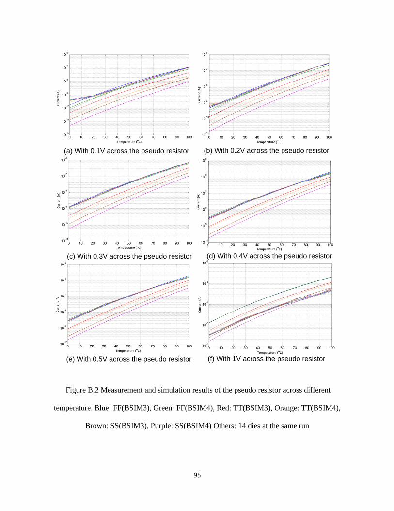
95
(a) With 0.1V across the pseudo resistor (b) With 0.2V across the pseudo resistor
(c) With 0.3V across the pseudo resistor (d) With 0.4V across the pseudo resistor
(e) With 0.5V across the pseudo resistor (f) With 1V across the pseudo resistor
Figure B.2 Measurement and simulation results of the pseudo resistor across different
temperature. Blue: FF(BSIM3), Green: FF(BSIM4), Red: TT(BSIM3), Orange: TT(BSIM4),
Brown: SS(BSIM3), Purple: SS(BSIM4) Others: 14 dies at the same run
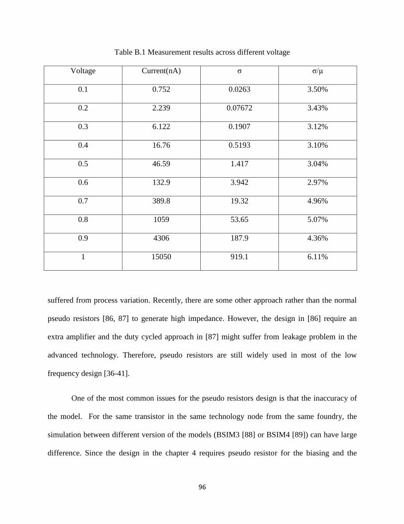
96
Table B.1 Measurement results across different voltage
Voltage Current(nA) σ σ/μ
0.1 0.752 0.0263 3.50%
0.2 2.239 0.07672 3.43%
0.3 6.122 0.1907 3.12%
0.4 16.76 0.5193 3.10%
0.5 46.59 1.417 3.04%
0.6 132.9 3.942 2.97%
0.7 389.8 19.32 4.96%
0.8 1059 53.65 5.07%
0.9 4306 187.9 4.36%
1 15050 919.1 6.11%
suffered from process variation. Recently, there are some other approach rather than the normal
pseudo resistors [86, 87] to generate high impedance. However, the design in [86] require an
extra amplifier and the duty cycled approach in [87] might suffer from leakage problem in the
advanced technology. Therefore, pseudo resistors are still widely used in most of the low
frequency design [36-41].
One of the most common issues for the pseudo resistors design is that the inaccuracy of
the model. For the same transistor in the same technology node from the same foundry, the
simulation between different version of the models (BSIM3 [88] or BSIM4 [89]) can have large
difference. Since the design in the chapter 4 requires pseudo resistor for the biasing and the

97
CMFB, a separate die to observe the pseudo resistor value for better design the corner frequency
is tapeout and measured.
B.2 Measurement Results and Conclusions
Figure B.2 and Table B.1 show the simulation and the measurement results of the pseudo
resistors. From Table B.1, the resistance is clearly highly nonlinear as it is shown in the equation
(B.3). Noted that under the same bias voltage the resistance is usually follow one of the model
correctly. At small voltage bias (<0.1V) to medium range voltage (around 0.5V which is the
usual bias point for full swing output), it follows the FF corner of the BSIM3 model. While
biased at high voltage (>1V), it follows SS corner of the BSIM3 model. The above results also
show that the current is expected to be larger at low bias and smaller at higher bias. From
equation (B.3), it implies that the coefficient n is not modeled well in the subthreshold region.

98
BIBLIOGRAPHY
99
[1] C. G. Bell, et al., "Effect of Technology on Near Term Computer Structures," in
Computer , vol.5, no.2, pp.29-38, Feb. 1972
[2] G. Moore, “Cramming More Components Onto Integrated Circuits," in Proceedings of
the IEEE , vol.86, no.1, pp.82-85, Jan. 1998
[3] R. H. Dennard, et al., "Design of ion-implanted MOSFET's with very small physical
dimensions," in IEEE Solid-State Circuits Society Newsletter, vol.12, no.1, pp.38-50,
Winter 2007
[4] T. Nakagawa, et al., "1-cc Computer: Cross-Layer Integration With UWB-IR
Communication and Locationing," in IEEE Journal of Solid-State Circuits, vol.43, no.4,
pp.964-973, April 2008
[5] G. Frantz, "Digital signal processor trends," in IEEE Micro, vol.20, no.6, pp.52-59,
Nov/Dec 2000
[6] N. Elvin, et al., "Feasibility of structural monitoring with vibration powered sensors", in
Smart Materials and Structures, vol. 15, pp.977 -986 2006
[7] L. Schwiebert, et al., "Research challenges in wireless networks of biomedical sensors",
in Int. Conf. Mobile Computing and Networking, pp.151 -165 2001
[8] B. Warneke, et al., "Smart dust: Communicating with a cubic-millimeter computer", in
Computer, vol. 34, pp.44 -51 2001
[9] G. Chen, et al., “A cubic-millimeter energy-autonomous wireless intraocular pressure
monitor,” in 2010 IEEE International Solid-State Circuits Conference Digest of
Technical Papers (ISSCC), Feb. 2010, pp. 310-312.
100
[10] G. Chen, et al., “Millimeter-scale nearly perpetual sensor system with stacked battery
and solar cells,” in 2011 IEEE International Solid-State Circuits Conference Digest of
Technical Papers (ISSCC), Feb. 2011, pp. 288-289.
[11] Y. Lee, et al., “A modular 1mm3 die-stacked sensing platform with optical
communication and multi-modal energy harvesting,” in 2012 IEEE International Solid-
State Circuits Conference Digest of Technical Papers (ISSCC), Feb. 2012, pp. 402-403.
[12] Y. Lee, et al., “A Modular 1 mm3 die-stacked sensing platform with low power I
2C
inter-die communication and multi-modal energy harvesting,” in IEEE Journal of Solid-
State Circuits, vol. 48, no. 1, pp. 229-242, Jan. 2013.
[13] J. Rabaey, et al., "Beyond the horizon: The next 10x reduction in power — Challenges
and solutions," in 2011 IEEE International Solid-State Circuits Conference Digest of
Technical Papers (ISSCC), vol., no., pp.31-31, 20-24 Feb. 2011
[14] W. Sansen, "Analog CMOS from 5 micrometer to 5 nanometer," in 2015 IEEE
International Solid-State Circuits Conference Digest of Technical Papers (ISSCC), 2015
IEEE International , vol., no., pp.1-6, 22-26 Feb. 2015
[15] W. M. C. Sansen, Analog Design Essentials, 2006 :Springer-Verlag
[16] Y.-P. Chen, et al., "A 2.98nW bandgap voltage reference using a self-tuning low leakage
sample and hold," in 2012 Symposium on VLSI Circuits (VLSIC), vol., no., pp.200-201,
13-15 June 2012
[17] Y.-P. Chen, et al., "45pW ESD clamp circuit for ultra-low power applications," in 2013
IEEE Custom Integrated Circuits Conference (CICC), vol., no., pp.1-4, 22-25 Sept.
2013
101
[18] C.-T. Wang, et al., "Design of Power-Rail ESD Clamp Circuit With Ultra-Low Standby
Leakage Current in Nanoscale CMOS Technology," in IEEE Journal of Solid-State
Circuits, vol.44, no.3, pp.956-964, March 2009
[19] P.-Y. Chiu, et al., "Design of low-leakage power-rail ESD clamp circuit with MOM
capacitor and STSCR in a 65-nm CMOS process," in 2011 IEEE International
Conference on IC Design & Technology (ICICDT), vol., no., pp.1-4, 2-4 May 2011
[20] M.-D. Ker, et al., "New Low-Leakage Power-Rail ESD Clamp Circuit in a 65-nm Low-
Voltage CMOS Process," in IEEE Transactions on Device and Materials Reliability,
vol.11, no.3, pp.474-483, Sept. 2011
[21] Y.-P. Chen, et al., "A 266nW multi-chopper amplifier with 1.38 noise efficiency factor
for neural signal recording," in 2014 Symposium on VLSI Circuits Digest of Technical
Papers, vol., no., pp.1-2, 10-13 June 2014
[22] Y.-P. Chen, et al., "An Injectable 64 nW ECG Mixed-Signal SoC in 65 nm for
Arrhythmia Monitoring," in IEEE Journal of Solid-State Circuits, vol.50, no.1, pp.375-
390, Jan. 2015
[23] R.F. Yazicioglu, et al., "A 30μW Analog Signal Processor ASIC for Portable
Biopotential Signal Monitoring," in IEEE Journal of Solid-State Circuits, vol.46, no.1,
pp.209-223, Jan. 2011
[24] G.D. Vita et al., “A Sub-1-V, 10ppm/°C, Nanopower Voltage Reference Generator,” In
IEEE Journal of Solid-State Circuits, pp.1536-1542, 2007.
[25] H.W. Huang et al., “A 1V 16.9ppm/°C 250nA Switched Capacitor CMOS Voltage
Reference,” in 2008 IEEE International Solid-State Circuits Conference, pp.438-439,
2008.
102
[26] K. Ueno et al., “A 300 nW, 15 ppm/°C, 20 ppm/V CMOS voltage reference circuit
consisting of subthreshold MOSFETs,” in IEEE Journal of Solid-State Circuits, vol. 44,
no. 7, pp. 2047–2054, Jul. 2009.
[27] A.-J. Annema, “Low power bandgap references featuring DTMOST’s,” in IEEE
Journal of Solid-State Circuits, vol. 34, pp. 949–955, July 1999.
[28] P. Kinget et al., “Voltage References for Ultra-Low Supply Voltages,” in 2008 IEEE
Custom Integrated Circuits Conference (CICC), pp.715-720, 2008.
[29] H. Tanaka et al., “Sub 1-μA dynamic reference voltage generator for battery-operated
DRAMs,” in IEEE Journal of Solid-State Circuits, vol. 29, pp. 448–453, Apr. 1994.
[30] B. K. Ahuja et al., “A 0.5μA Precision CMOS Floating Gate Analog Reference,” in
2005 IEEE International Solid-State Circuits Conference, pp. 286-287, February 2005.
[31] M.-D. Ker. et al., "ESD Protection for Mixed-Voltage I/O in LowVoltage Thin-Oxide
CMOS," in 2006 IEEE International Solid-State Circuits Conference Digest of
Technical Papers, vol., no., pp.2230-2237, 6-9 Feb. 2006
[32] M.-D. Ker, et al., "On the design of power-rail esd clamp circuit with consideration of
gate leakage current in 65-nm low-voltage CMOS process," in 2009 IEEE International
Symposium on Circuits and Systems (ISCAS), vol., no., pp.2281-2284, 24-27 May 2009
[33] Texas Instruments Inc., MSP430F20X1, MSP430F20X2, MSP430F20X3 Mixed Signal
Microcontroller (Rev. H), 2011
[34] J. Li et al., "Technology scaling of advanced bulk CMOS on-chip ESD protection down
to the 32nm node," in 2009 31st EOS/ESD Symposium, vol., no., pp.1-7, Aug. 30 -Sept.
4 2009
103
[35] S. Bang, et al., "Reconfigurable sleep transistor for GIDL reduction in ultra-low standby
power systems," in 2012 IEEE Custom Integrated Circuits Conference (CICC), vol.,
no., pp.1-4, 9-12 Sept. 2012
[36] N. V. Helleputte, et al., "A 160μA biopotential acquisition ASIC with fully integrated
IA and motion-artifact suppression," in 2012 IEEE International Solid-State Circuits
Conference Digest of Technical Papers (ISSCC) , vol., no., pp.118-120, 19-23 Feb.
2012
[37] W.-M. Chen, et al., "A fully integrated 8-channel closed-loop neural-prosthetic SoC for
real-time epileptic seizure control," in 2013 IEEE International Solid-State Circuits
Conference Digest of Technical Papers (ISSCC) , vol., no., pp.286-287, 17-21 Feb.
2013
[38] D. Han, et al., "A 0.45V 100-channel neural-recording IC with sub-µW/channel
consumption in 0.18µm CMOS," in 2013 IEEE International Solid-State Circuits
Conference Digest of Technical Papers (ISSCC), vol., no., pp.290-291, 17-21 Feb.
2013
[39] Q. Fan, et al., "A 1.8µW 60 nV/√𝐻𝑧 Capacitively-Coupled Chopper Instrumentation
Amplifier in 65 nm CMOS for Wireless Sensor Nodes," In IEEE Journal of Solid-State
Circuits, vol.46, no.7, pp.1534,1543, July 2011
[40] B. Johnson, et al., "An Orthogonal Current-Reuse Amplifier for Multi-Channel
Sensing," in IEEE Journal of Solid-State Circuits, vol.48, no.6, pp.1487-1496, June
2013
104
[41] J. Holleman, et al., "A Sub-Microwatt Low-Noise Amplifier for Neural Recording," in
2007 29th Annual International Conference of the IEEE Engineering in Medicine and
Biology Society (EMBS), vol., no., pp.3930-3933, 22-26 Aug. 2007
[42] A. Shukla, et al., “Avoiding permanent atrial fibrillation: treatment approaches to
prevent disease progression” [Online]. Available:
http://www.ncbi.nlm.nih.gov/pmc/articles/PMC3872084/
[43] L.S.Y. Wong, et al., "A very low-power CMOS mixed-signal IC for implantable
pacemaker applications," in IEEE Journal of Solid-State Circuits, vol.39, no.12,
pp.2446,2456, Dec. 2004
[44] A. Berson, et al., “Skin–electrode impedance problems in electrocardiography,” in
Journal of Am. Heart, vol. 76, no. 4, pp. 514–525, October 1968.
[45] M. S. Spach, et al., “Skin-electrode impedance and its effect on recording cardiac
potentials,” in Circulation, vol. 34, 1966, pp. 649 – 656.
[46] J. Rosell, et al., “Skin impedance from 1 Hz to 1 MHz,” in IEEE Transaction on
Biomedical Engineering, vol. 35, no. 8, pp. 649 – 651, August 1988.
[47] C. Zellerhoff, et al., “How can we identify the best implantation site for an ECG event
recorder?,” Ii Pacing & Clinical Electrophys, pp. 1545-1549, 2000.
[48] X. Zou, et al., “A 1-V 450-nW Fully Integrated Programmable Biomedical Sensor
Interface Chip,” in IEEE Journal of Solid-State Circuits, vol. 44, no. 4. pp. 1067–1077,
2009.
[49] M. Yip, et al., "A 0.6V 2.9µW mixed-signal front-end for ECG monitoring," in 2012
Symposium on VLSI Circuits (VLSIC), vol., no., pp.66,67, 13-15 June 2012
105
[50] S.-Y. Hsu, et al., "A sub-100µW multi-functional cardiac signal processor for mobile
healthcare applications," in 2012 Symposium on VLSI Circuits (VLSIC), vol., no.,
pp.156,157, 13-15 June 2012
[51] S. Kim, et al., "A 20µW intra-cardiac signal-processing IC with 82dB bio-impedance
measurement dynamic range and analog feature extraction for ventricular fibrillation
detection," in 2013 IEEE International Solid-State Circuits Conference Digest of
Technical Papers (ISSCC), vol., no., pp.302,303, 17-21 Feb. 2013
[52] X. Liu, et al., "A 457-nW cognitive multi-functional ECG processor," in 2013 IEEE
Asian Solid-State Circuits Conference (A-SSCC), vol., no., pp.141,144, 11-13 Nov. 2013
[53] C.J. Deepu, et al., "An ECG-SoC with 535nW/channel lossless data compression for
wearable sensors," in 2013 IEEE Asian Solid-State Circuits Conference (A-SSCC), vol.,
no., pp.145,148, 11-13 Nov. 2013
[54] Y. Long, et al., "A 680nA fully integrated implantable ECG-acquisition IC with analog
feature extraction," in 2014 IEEE International Solid-State Circuits Conference Digest
of Technical Papers (ISSCC), pp. 418,419, 2014.
[55] D. Jeon, et al., "An implantable 64nW ECG-monitoring mixed-signal SoC for
arrhythmia diagnosis," in 2014 IEEE International Solid-State Circuits Conference
Digest of Technical Papers (ISSCC), vol., no., pp.416,417, 9-13 Feb. 2014
[56] John G. Webster, Medical Instrumentation Application and Design, Wiley Press, 2009
[57] ANSI/AAMI-EC13, American National Standards for Cardiac Monitors, Hearth Rate
Meters and Alarms, 2002.
[58] Hakan Oral, et al., “Atrial Fibrillation Classification Using Power Measurement,” U.S.
Patent 20130197380 A1, Aug, 1, 2013.
106
[59] C. Enz, “Circuit techniques for reducing the effects of op-amp imperfections:
autozeroing, correlated double sampling, and chopper stabilization,” in Proceedings of
the IEEE, no. 11, vol. 84, pp. 1584–1614, 1996
[60] T. Denison, et al., "A 2.2µW 94nV/√Hz, Chopper-Stabilized Instrumentation Amplifier
for EEG Detection in Chronic Implants," in 2007 IEEE International Solid-State
Circuits Conference Digest of Technical Papers (ISSCC), vol., no., pp.162, 11-15 Feb.
2007
[61] M. Chae, et al., "A 128-Channel 6mW Wireless Neural Recording IC with On-the-Fly
Spike Sorting and UWB Tansmitter," in 2008 IEEE International Solid-State Circuits
Conference (ISSCC), vol., no., pp.146,603, 3-7 Feb. 2008
[62] A. T. Do, et al., "A 160nW 25 kS/s 9-bit SAR ADC for neural signal recording
applications," in 2012 IEEE 10th International New Circuits and Systems Conference
(NEWCAS), vol., no., pp.525,528, 17-20 June 2012
[63] D. Zhang, et al., "A 53-nW 9.1-ENOB 1-kS/s SAR ADC in 0.13-um CMOS for Medical
Implant Devices," in IEEE Journal of Solid-State Circuits, vol.47, no.7, pp.1585,1593,
July 2012
[64] D. Zhang, et al., "A 3-nW 9.1-ENOB SAR ADC at 0.7 V and 1 kS/s," in 2012
Proceedings of the ESSCIRC (ESSCIRC), vol., no., pp.369,372, 17-21 Sept. 2012
[65] P. J. A. Harpe, et al., "A 26µW 8 bit 10 MS/s Asynchronous SAR ADC for Low Energy
Radios," in IEEE Journal of Solid-State Circuits, vol.46, no.7, pp.1585,1595, July 2011
[66] T. Wakimoto, et al., “Statistical analysis on the effect of capacitance mismatch in a
high-resolution successive-approximation ADC”, in IEEJ Transaction. on Electrical
and Electronic Engineering, vol. 6, pp. s89–s93, 2011.
107
[67] H. Zhang, et al., "Design of an ultra-low power SAR ADC for biomedical applications,"
2010 10th IEEE International Conference on Solid-State and Integrated Circuit
Technology (ICSICT), vol., no., pp.460,462, 1-4 Nov. 2010
[68] J. Pan et al., “A Real-Time QRS Detection Algorithm,“ in IEEE Transactions on
Biomedical Engineering , vol.BME-32, no.3, pp.230,236, March 1985
[69] B. Zhai, et al., “Analysis and mitigation of variability in subthreshold design,” in 2005
International Symposium on Low Power Electronics and Design(ISLPED), Aug. 2005,
pp. 20–25.
[70] A. Wang, et al., “A 180-mV subthreshold FFT processor using a minimum energy
design methodology,” in IEEE Journal of Solid-State Circuits, vol. 40, no. 1, pp. 310–
319, Jan. 2005.
[71] Y. Zhang, et al., "A Batteryless 19µW MICS/ISM-Band Energy Harvesting Body
Sensor Node SoC for ExG Applications," in IEEE Journal of Solid-State Circuits,
vol.48, no.1, pp.199,213, Jan. 2013
[72] W. H. Hsieh, et al., "A micromachined thin-film Teflon electret microphone," in 1997
International Conference on Solid State Sensors and Actuators, vol.1, no., pp.425-428
vol.1, 16-19 Jun 1997
[73] InvenSense Inc., ICS-40310 Ultra-low Current, Low-Noise Microphone with Analog
Output , 2014
[74] Knowles Inc., SPV1840LR5H-B Zero-Height SiSonicTM
Microphone, 2014
[75] J. Citakovic, et al., "A compact CMOS MEMS microphone with 66dB SNR," in 2009
IEEE International Solid-State Circuits Conference Digest of Technical Papers,
(ISSCC), vol., no., pp.350-351,351a, 8-12 Feb. 2009
108
[76] J. V. D. Boom, "A 50μW biasing feedback loop with 6ms settling time for a MEMS
microphone with digital output," in 2012 IEEE International Solid-State Circuits
Conference Digest of Technical Papers (ISSCC), vol., no., pp.200-202, 19-23 Feb. 2012
[77] S. Ersoy, et al., "A 0.25mm2 AC-biased MEMS microphone interface with 58dBA
SNR," in 2013 IEEE International Solid-State Circuits Conference Digest of Technical
Papers (ISSCC), vol., no., pp.382-383, 17-21 Feb. 2013
[78] ETSI, EN 300 969 - Half rate speech transcoding (GSM 06.20 version 8.0.1), 1999
[79] C. C. Tu, et al., "Measurement and parameter characterization of pseudo-resistor based
CCIA for biomedical applications," in Bioelectronics and Bioinformatics (ISBB), 2014
IEEE International Symposium on , vol., no., pp.1-4, 11-14 April 2014
[80] M. T. Shiue, et al., "Tunable high resistance voltage-controlled pseudo-resistor with
wide input voltage swing capability," in Electronics Letters, vol.47, no.6, pp.377-378,
March 17 2011
[81] Y.-C. Huang, et al., "A novel pseudo resistor structure for biomedical front-end
amplifiers," in 2015 37th Annual International Conference of the IEEE Engineering in
Medicine and Biology Society (EMBC), vol., no., pp.2713-2716, 25-29 Aug. 2015
[82] K.-W. Yao, et al., "Design of a neural recording amplifier with tunable pseudo
resistors," in 2011 IEEE International SOC Conference (SOCC), vol., no., pp.376-379,
26-28 Sept. 2011
[83] X. Xi et al., “BSIM4.3.0 MOSFET Model – User Manual,” Department of Electrical
and Computer Engineering, University of California, Berkeley, 2003.
[84] A. Shrivastava, K. Craig, N. E. Roberts, D. D. Wentzloff and B. H. Calhoun, "5.4 A
32nW bandgap reference voltage operational from 0.5V supply for ultra-low power

109
systems," 2015 IEEE International Solid-State Circuits Conference - (ISSCC) Digest of
Technical Papers, San Francisco, CA, 2015, pp. 1-3.
[85] J. M. Lee et al., "5.7 A 29nW bandgap reference circuit," 2015 IEEE International
Solid-State Circuits Conference - (ISSCC) Digest of Technical Papers, San Francisco,
CA, 2015, pp. 1-3.
[86] G. Ferrari, D. Bianchi, A. Rottigni and M. Sampietro, "17.4 CMOS impedance analyzer
for nanosamples investigation operating up to 150MHz with Sub-aF resolution," 2014
IEEE International Solid-State Circuits Conference Digest of Technical Papers (ISSCC),
San Francisco, CA, 2014, pp. 292-293.
[87] H. Chandrakumar and D. Marković, "5.5 A 2µW 40mVpp linear-input-range chopper-
stabilized bio-signal amplifier with boosted input impedance of 300MΩ and electrode-
offset filtering," 2016 IEEE International Solid-State Circuits Conference (ISSCC), San
Francisco, CA, 2016, pp. 96-97.
[88] Y. Cheng and C. Hu, “MOSFET Modeling and BSIM3 User’s Guide.” Norwell, MA:
Kluwer Academic, 1999.
[89] W. Liu, “MOSFET Models for SPICE Simulations Including BSIM3v3 and BSIM4”
New York, NY, USA: Wiley, 2001.
[90] Crossbow-Technology. eKo Pro Series System for Environmental Monitoring.
http://www.xbow.com/Eko/index.aspx, 2008.
[91] Freescale-Semiconductor. MPXY8300; Microcontroller, Presure Sensor, X-Z
Accelerometer and RF Transmitter. http://www.freescale.com/, 2008.
110
[92] Cardio MEMS. EndoSure Wireless AAA Pressure Sensor. http://www.cardiomems.com,
2008.
[93] E.T. Zellers, S. Reidy, R.A. Veeneman, R. Gordenker, W.H. Steinecker, G.R.
Lambertus, Hanseup Kim, J.A. Potkay, M.P. Rowe, Qiongyan Zhong, C. Avery, H.K.L.
Chan, R.D. Sacks, K. Najafi, and K.D. Wise. “An integrated micro analytical system for
complex vapor mixtures.” pages 1491 –1496, jun. 2007.
[94] P. V. Rajesh et al., "22.4 A 172μW compressive sampling photoplethysmographic
readout with embedded direct heart-rate and variability extraction from compressively
sampled data," 2016 IEEE International Solid-State Circuits Conference (ISSCC), San
Francisco, CA, 2016, pp. 386-387.
[95] J. B. Bates, N. J. Dudney, B. Neudecker, A. Ueda, and C. D. Evans. Thin-film lithium
and lithium-ion batteries. Solid State Ionics, 135(1-4):33 – 45, 2000.
[96] G. Chen et al., "A cubic-millimeter energy-autonomous wireless intraocular pressure
monitor," 2011 IEEE International Solid-State Circuits Conference, San Francisco, CA,
2011, pp. 310-312.
Related Documents