cpe 252: Computer Organization 1 Lo’ai Tawalbeh Lecture #4 Register Transfer and Microoperations 23/2/2006 Chapter 4:

Lo’ai Tawalbeh Lecture #4
Jan 21, 2016
Chapter 4:. Lo’ai Tawalbeh Lecture #4. Register Transfer and Microoperations. 23/2/2006. contents. • Register Transfer Language • Register Transfer • Bus and Memory Transfers • Arithmetic Microoperations • Logic Microoperations • Shift Microoperations • Arithmetic Logic Shift Unit. - PowerPoint PPT Presentation
Welcome message from author
This document is posted to help you gain knowledge. Please leave a comment to let me know what you think about it! Share it to your friends and learn new things together.
Transcript

cpe 252: Computer Organization 1
Lo’ai Tawalbeh
Lecture #4
Register Transfer and Microoperations
23/2/2006
Chapter 4:
cpe 252: Computer Organization 2
contents
• Register Transfer Language
• Register Transfer
• Bus and Memory Transfers
• Arithmetic Microoperations
• Logic Microoperations
• Shift Microoperations
• Arithmetic Logic Shift Unit

cpe 252: Computer Organization 3
4-1 Register Transfer Language (RTL)
• Digital System: An interconnection of hardware modules that do a certain task on the information.
• Registers + Operations performed on the data stored in them = Digital Module
• Modules are interconnected with common data and control paths to form a digital computer system
cpe 252: Computer Organization 4
4-1 Register Transfer Language cont.
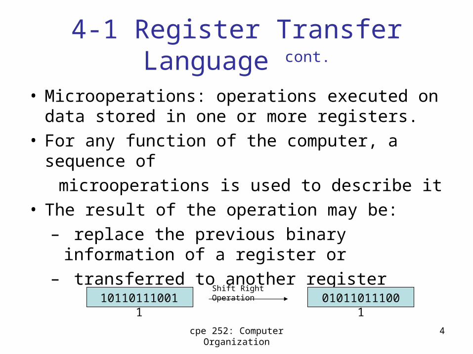
• Microoperations: operations executed on data stored in one or more registers.
• For any function of the computer, a sequence of
microoperations is used to describe it• The result of the operation may be:
– replace the previous binary information of a register or
– transferred to another register101101110011 010110111001
Shift Right Operation
cpe 252: Computer Organization 5
4-1 Register Transfer Language cont.
• The internal hardware organization of a digital computer is defined by specifying:
• The set of registers it contains and their function• The sequence of microoperations performed on
the binary information stored in the registers• The control that initiates the sequence of
microoperations
• Registers + Microoperations Hardware + Control Functions = Digital Computer
cpe 252: Computer Organization 6
4-1 Register Transfer Language cont.
• Register Transfer Language (RTL) : a symbolic notation to describe the microoperation transfers among registers
Next steps:– Define symbols for various types of microoperations, – Describe the hardware that implements these
microoperations
cpe 252: Computer Organization 7
4-2 Register Transfer (our first microoperation)
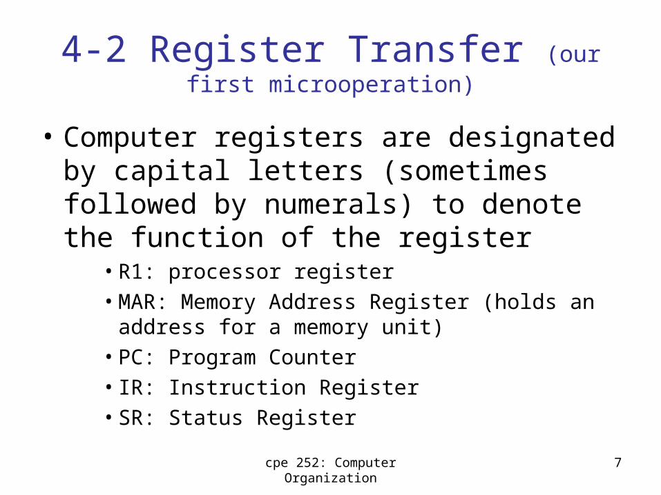
• Computer registers are designated by capital letters (sometimes followed by numerals) to denote the function of the register
• R1: processor register• MAR: Memory Address Register (holds an address
for a memory unit)• PC: Program Counter• IR: Instruction Register• SR: Status Register

cpe 252: Computer Organization 8
4-2 Register Transfer cont.
• The individual flip-flops in an n-bit register are numbered in sequence from 0 to n-1 (from the right position toward the left position)
R1 7 6 5 4 3 2 1 0
A block diagram of a register
Register R1 Showing individual bits
cpe 252: Computer Organization 9
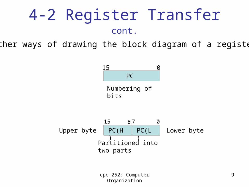
4-2 Register Transfer cont.
PC
Numbering of bits
Partitioned into two parts
15 0
PC(H) PC(L)
07815
Lower byteUpper byte
Other ways of drawing the block diagram of a register:

cpe 252: Computer Organization 10
4-2 Register Transfer cont.
• Information transfer from one register to another is described by a replacement operator: R2 ← R1• This statement denotes a transfer of the content of
register R1 into register R2• The transfer happens in one clock cycle• The content of the R1 (source) does not change• The content of the R2 (destination) will be lost and
replaced by the new data transferred from R1• We are assuming that the circuits are available from the
outputs of the source register to the inputs of the destination register, and that the destination register has a parallel load capability
cpe 252: Computer Organization 11
4-2 Register Transfer cont.
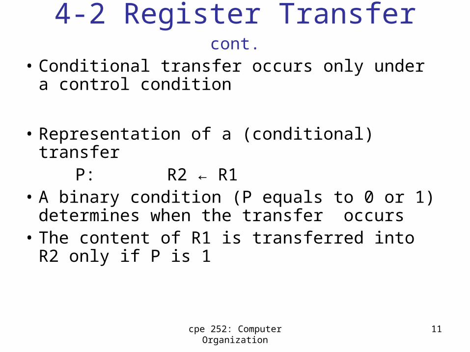
• Conditional transfer occurs only under a control condition
• Representation of a (conditional) transfer P: R2 ← R1• A binary condition (P equals to 0 or 1)
determines when the transfer occurs• The content of R1 is transferred into R2
only if P is 1

cpe 252: Computer Organization 12
4-2 Register Transfer cont.
n
Clock
R1
R2Control Circuit
Load
t t+1
Clock
LoadTransfer occurs here
Synchronized with the clock
P
Hardware implementation of a controlled transfer: P: R2 ← R1
Block diagram:
Timing diagram
cpe 252: Computer Organization 13
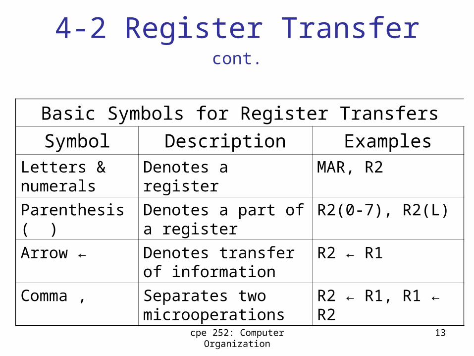
4-2 Register Transfer cont.
Basic Symbols for Register Transfers
Symbol Description ExamplesLetters & numerals
Denotes a register MAR, R2
Parenthesis ( ) Denotes a part of a register
R2(0-7), R2(L)
Arrow ← Denotes transfer of information
R2 ← R1
Comma , Separates two microoperations
R2 ← R1, R1 ← R2
cpe 252: Computer Organization 14
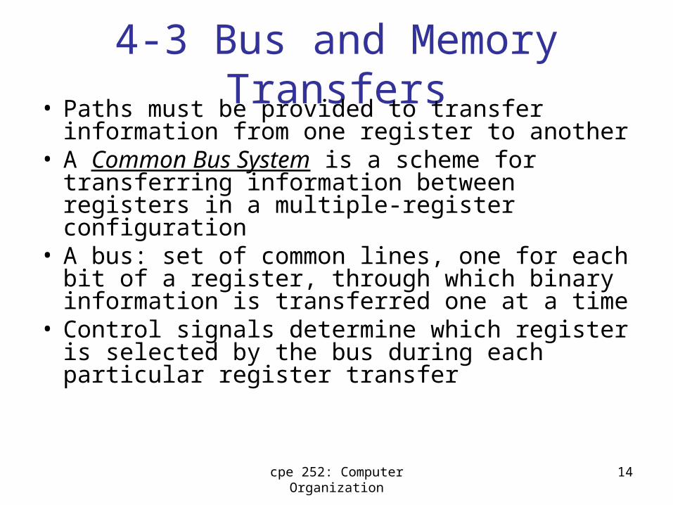
4-3 Bus and Memory Transfers• Paths must be provided to transfer information
from one register to another• A Common Bus System is a scheme for
transferring information between registers in a multiple-register configuration
• A bus: set of common lines, one for each bit of a register, through which binary information is transferred one at a time
• Control signals determine which register is selected by the bus during each particular register transfer

cpe 252: Computer Organization 15
4-3 Bus and Memory Transfers
3 2 1 0
Register D
D3 D2 D1 D0
3 2 1 0
Register C
C3 C2 C1 C0
3 2 1 0
Register B
B3 B2 B1 B0
3 2 1 0
Register A
A3 A2 A1 A0
D3 C3 B3 A3
S0
S1MUX33 2 1 0
D2 C2 B2 A2
S0
S1MUX2
3 2 1 0
D1 C1 B1 A1
S0
S1MUX1
3 2 1 0
D0 C0 B0 A0
S0
S1MUX0
3 2 1 0
4-Line Common Bus
Register A Register B Register C Register D
Bus lines

cpe 252: Computer Organization 16
4-3 Bus and Memory Transfers• The transfer of information from a bus into one of
many destination registers is done:– By connecting the bus lines to the inputs of all destination
registers and then:– activating the load control of the particular destination
register selected
• We write: R2 ← C to symbolize that the content of register C is loaded into the register R2 using the common system bus
• It is equivalent to: BUS ←C, (select C)
R2 ←BUS (Load R2)
cpe 252: Computer Organization 17
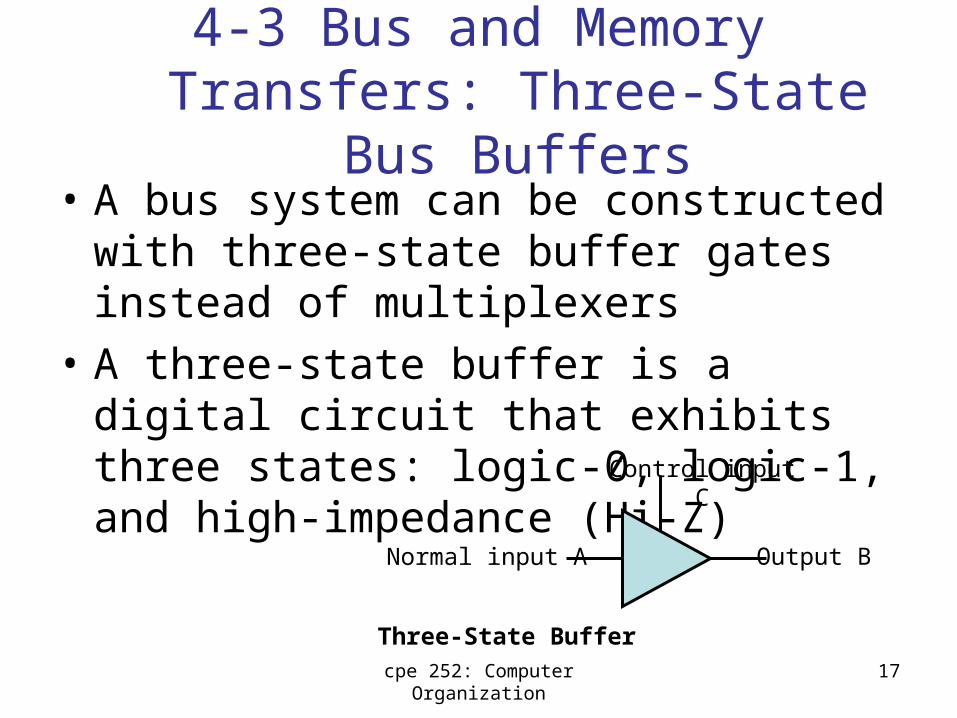
4-3 Bus and Memory Transfers: Three-State Bus Buffers
• A bus system can be constructed with three-state buffer gates instead of multiplexers
• A three-state buffer is a digital circuit that exhibits three states: logic-0, logic-1, and high-impedance (Hi-Z)
Normal input A
Control input C
Three-State Buffer
Output B
cpe 252: Computer Organization 18
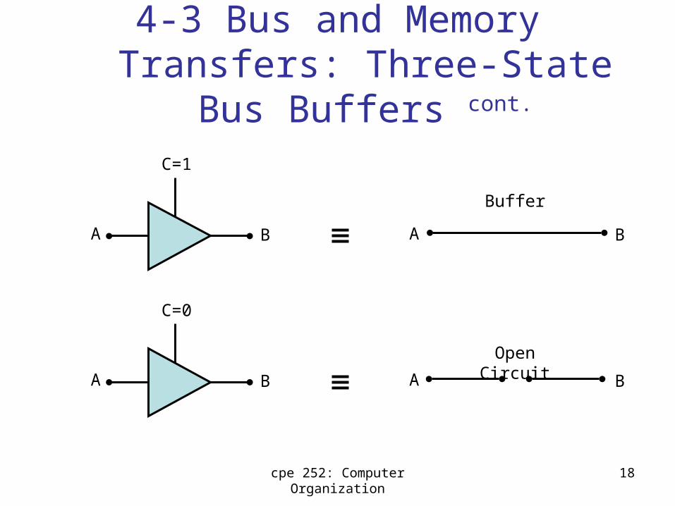
4-3 Bus and Memory Transfers: Three-State Bus Buffers cont.
A
C=1
B A B
A
C=0
B A B
Buffer
Open Circuit

cpe 252: Computer Organization 19
4-3 Bus and Memory Transfers: Three-State Bus Buffers cont.
2×4 Decoder
Select
Enable
0
1
2
3
S1
S0
E
Bus line for bit 0A0
B0
C0
D0
Bus line with three-state buffer (replaces MUX0 in the previous diagram)

cpe 252: Computer Organization 20
4-3 Bus and Memory Transfers: Memory Transfer
• Memory read : Transfer from memory• Memory write : Transfer to memory• Data being read or wrote is called a memory word
(called M)- (refer to section 2-7) • It is necessary to specify the address of M when
writing /reading memory• This is done by enclosing the address in square
brackets following the letter M• Example: M[0016] : the memory contents at
address 0x0016
cpe 252: Computer Organization 21
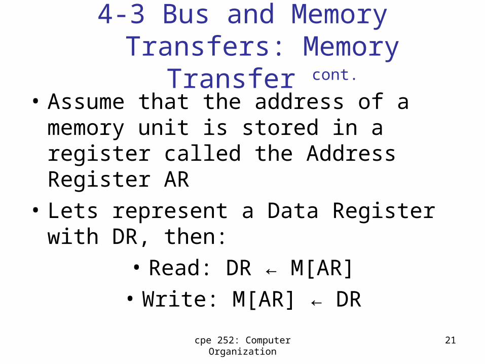
4-3 Bus and Memory Transfers: Memory Transfer cont.
• Assume that the address of a memory unit is stored in a register called the Address Register AR
• Lets represent a Data Register with DR, then:
• Read: DR ← M[AR]
• Write: M[AR] ← DR

cpe 252: Computer Organization 22
4-3 Bus and Memory Transfers: Memory Transfer cont.
AR
x12x0C
x0Ex10
x12x14
x16x18
19
3445
660
1322R1←M[AR]
R1100
R1
66
RAM
R1100

cpe 252: Computer Organization 23
4-4 Arithmetic Microoperations
• The microoperations most often encountered in digital computers are classified into four categories:– Register transfer microoperations– Arithmetic microoperations (on numeric data
stored in the registers)– Logic microoperations (bit manipulations on
non-numeric data)– Shift microoperations
cpe 252: Computer Organization 24
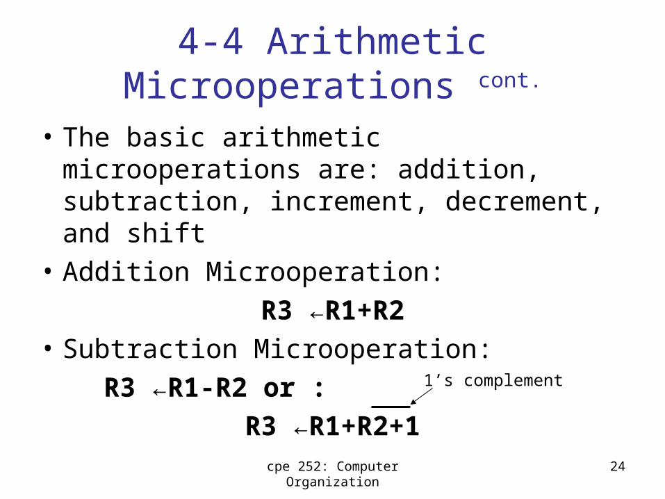
• The basic arithmetic microoperations are: addition, subtraction, increment, decrement, and shift
• Addition Microoperation:
R3 ←R1+R2
• Subtraction Microoperation:
R3 ←R1-R2 or :
R3 ←R1+R2+1
4-4 Arithmetic Microoperations cont.
1’s complement
cpe 252: Computer Organization 25
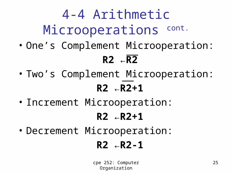
• One’s Complement Microoperation:
R2 ←R2• Two’s Complement Microoperation:
R2 ←R2+1• Increment Microoperation:
R2 ←R2+1• Decrement Microoperation:
R2 ←R2-1
4-4 Arithmetic Microoperations cont.

cpe 252: Computer Organization 26
Half Adder/Full AdderHalf Adder
0 0 0 0 00 0 1 0 10 1 0 0 10 1 1 1 01 0 0 0 11 0 1 1 01 1 0 1 01 1 1 1 1
cn = xy + xcn-1+ ycn-1
= xy + (x y)cn-1
s = x’y’cn-1+x’yc’n-1+xy’c’n-1+xycn-1
= x y cn-1 = (x y) cn-1
x
y
cn-1
x
y
cn-1
cn s
c = xy s = xy’ + x’y = x y
xy c
s
xy
cn-1
S
cn
Full Adder
0 0 0 00 1 0 11 0 0 11 1 1 0
x y c s
x y cn-1 cn s0
0
10
0
1
11
0
1
0
1
1
0
10
cpe 252: Computer Organization 27
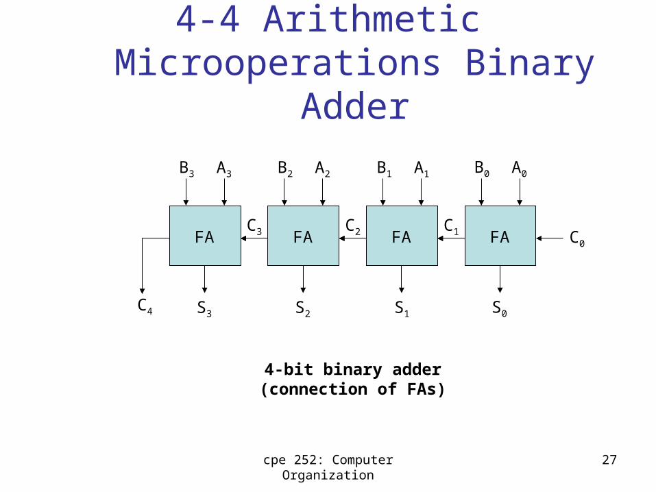
4-4 Arithmetic Microoperations Binary Adder
FAFAFAFA C0
A0B0
S0
A1B1
S1
A2B2
S2
A3B3
S3
C1C2C3
C4
4-bit binary adder (connection of FAs)

cpe 252: Computer Organization 28
4-4 Arithmetic Microoperations Binary Adder-Subtractor
FAFAFAFAC0
A0B0
S0
A1B1
S1
A2B2
S2
A3B3
S3
C1C2C3
C4
4-bit adder-subtractor
M
cpe 252: Computer Organization 29
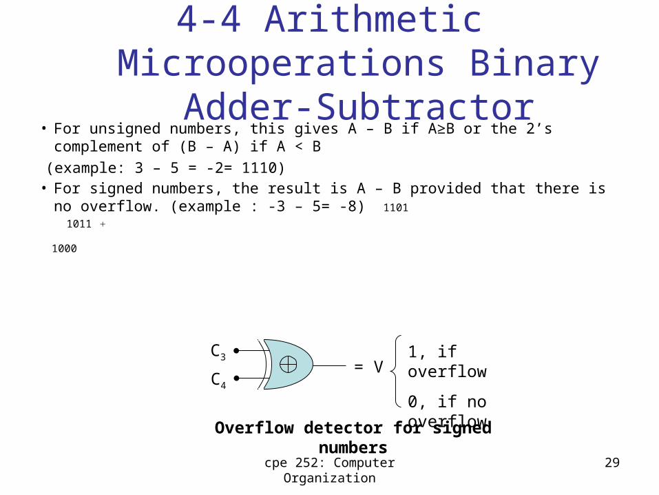
• For unsigned numbers, this gives A – B if A≥B or the 2’s complement of (B – A) if A < B
(example: 3 – 5 = -2= 1110)• For signed numbers, the result is A – B provided that there is no overflow.
(example : -3 – 5= -8) 1101
1011 + ـــــــــــــــــــــــــــ
1000
4-4 Arithmetic Microoperations Binary Adder-Subtractor
C3
C4
V= 1, if overflow
0, if no overflow
Overflow detector for signed numbers

cpe 252: Computer Organization 30
4-4 Arithmetic Microoperations Binary Adder-Subtractor cont.
• What is the range of unsigned numbers that can be represented in 4 bits?
• What is the range of signed numbers that can be represented in 4 bits?
• Repeat for n-bit?!
cpe 252: Computer Organization 31
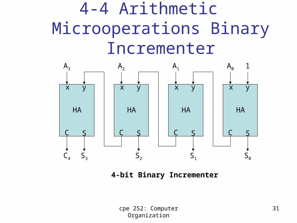
4-4 Arithmetic Microoperations Binary Incrementer
C S
x y
HA
C S
x y
HA
C S
x y
HA
C S
x y
HA
S0S1S2S3C4
1A0A1A2A3
4-bit Binary Incrementer
cpe 252: Computer Organization 32
4-4 Arithmetic Microoperations Binary Incrementer
• Binary Incrementer can also be implemented using a counter
• A binary decrementer can be implemented by adding 1111 to the desired register each time!
cpe 252: Computer Organization 33
4-4 Arithmetic Microoperations Arithmetic Circuit
• This circuit performs seven distinct arithmetic operations and the basic component of it is the parallel adder
• The output of the binary adder is calculated from the following arithmetic sum:
• D = A + Y + Cin
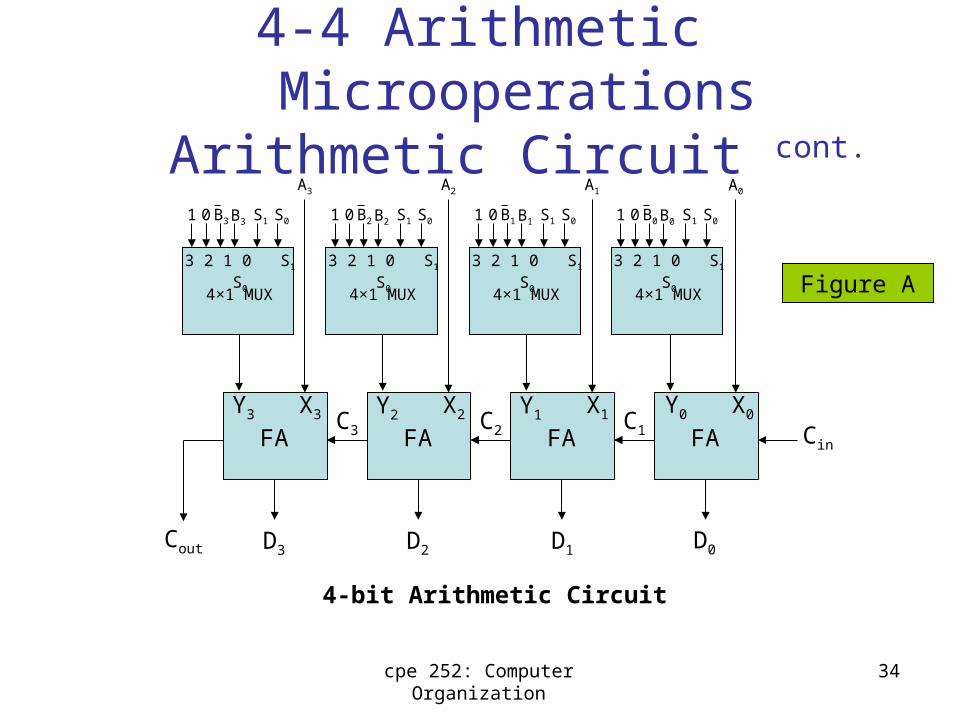
cpe 252: Computer Organization 34
B0
4-4 Arithmetic Microoperations Arithmetic Circuit cont.
3 2 1 0 S1 S0
4×1 MUX
FAFAFAFA Cin
D0D1D2D3
C1C2C3
Cout
B01 0 S1 S0B1
3 2 1 0 S1 S0
4×1 MUX
B11 0 S1 S0B2
3 2 1 0 S1 S0
4×1 MUX
B21 0 S1 S0B3
3 2 1 0 S1 S0
4×1 MUX
B31 0 S1 S0
A0A1A2A3
4-bit Arithmetic Circuit
X0Y0X1Y1X2Y2X3Y3
Figure A

cpe 252: Computer Organization 35
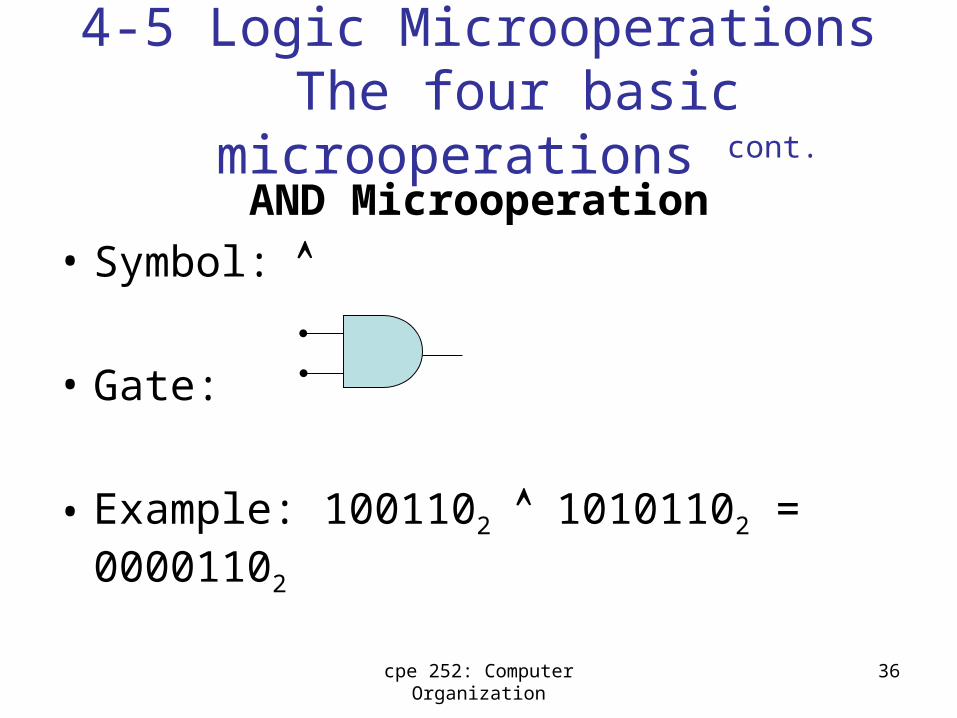
4-5 Logic MicrooperationsThe four basic microoperations
OR Microoperation• Symbol: , +
• Gate:
• Example: 1001102 10101102 = 11101102
P+Q: R1←R2+R3, R4←R5 R6
OR OR
ADD
cpe 252: Computer Organization 36
4-5 Logic MicrooperationsThe four basic microoperations
cont.
AND Microoperation
• Symbol:
• Gate:
• Example: 1001102 10101102 = 00001102
cpe 252: Computer Organization 37
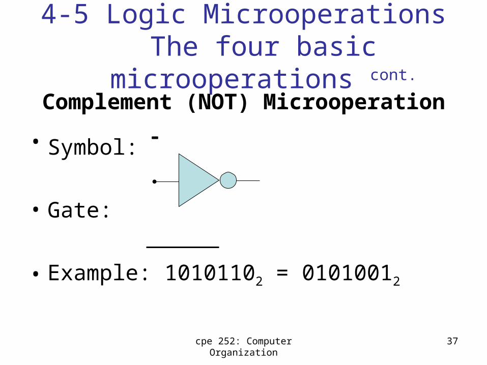
4-5 Logic MicrooperationsThe four basic microoperations
cont.
Complement (NOT) Microoperation
• Symbol:
• Gate:
• Example: 10101102 = 01010012

cpe 252: Computer Organization 38
4-5 Logic MicrooperationsThe four basic microoperations
cont.
XOR (Exclusive-OR) Microoperation
• Symbol:
• Gate:
• Example: 1001102 10101102 = 11100002
cpe 252: Computer Organization 39
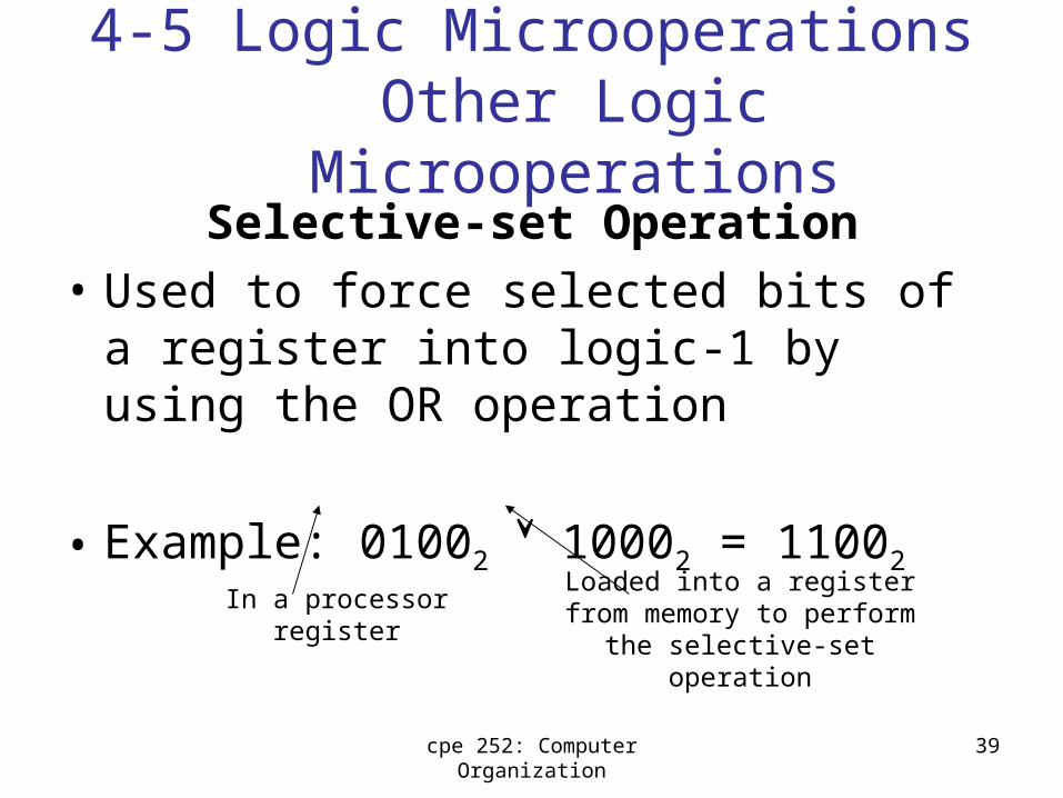
4-5 Logic MicrooperationsOther Logic Microoperations
Selective-set Operation
• Used to force selected bits of a register into logic-1 by using the OR operation
• Example: 01002 10002 = 11002
In a processor registerLoaded into a register from
memory to perform the selective-set operation
cpe 252: Computer Organization 40
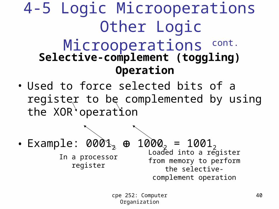
4-5 Logic MicrooperationsOther Logic Microoperations cont.
Selective-complement (toggling) Operation• Used to force selected bits of a register to be
complemented by using the XOR operation
• Example: 00012 10002 = 10012
In a processor registerLoaded into a register from
memory to perform the selective-complement operation

cpe 252: Computer Organization 41
4-5 Logic MicrooperationsOther Logic Microoperations cont.
Insert Operation• Step1: mask the desired bits• Step2: OR them with the desired value • Example: suppose R1 = 0110 1010, and we
desire to replace the leftmost 4 bits (0110) with 1001 then:
– Step1: 0110 1010 0000 1111– Step2: 0000 1010 1001 0000
R1 = 1001 1010
cpe 252: Computer Organization 42
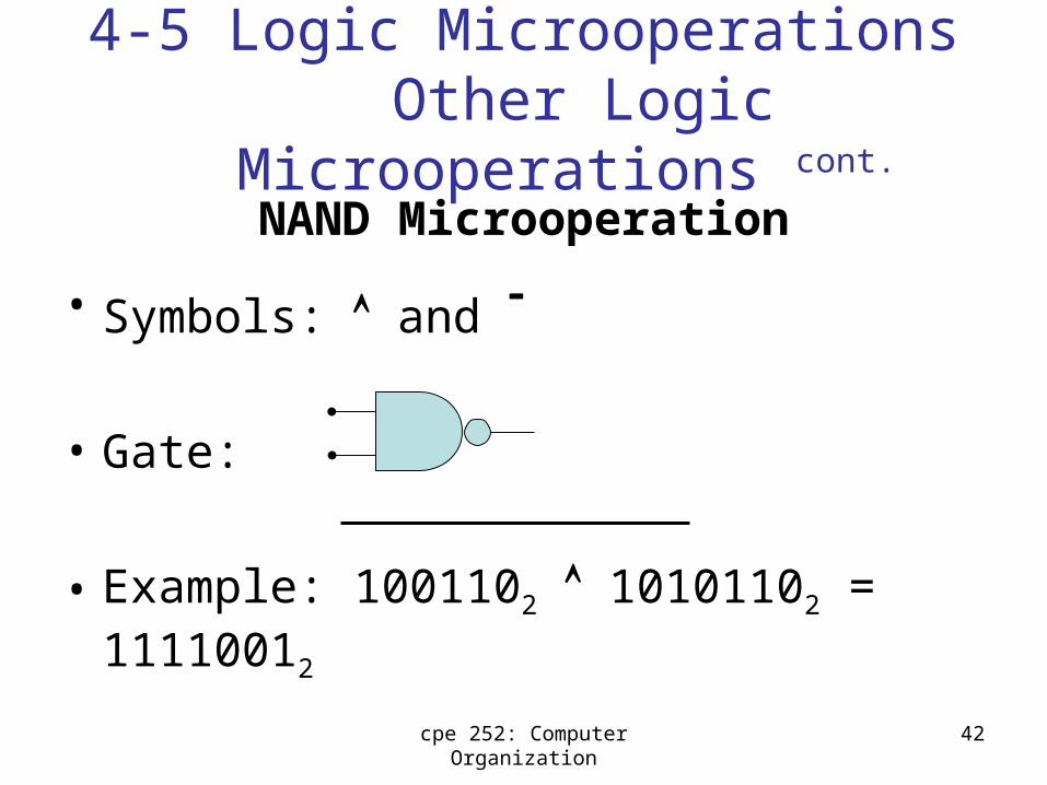
4-5 Logic Microoperations Other Logic Microoperations cont.
NAND Microoperation
• Symbols: and
• Gate:
• Example: 1001102 10101102 = 11110012

cpe 252: Computer Organization 43
4-5 Logic Microoperations Other Logic Microoperations cont.
NOR Microoperation
• Symbols: and
• Gate:
• Example: 1001102 10101102 = 00010012

cpe 252: Computer Organization 44
4-5 Logic Microoperations Other Logic Microoperations cont.
Set (Preset) Microoperation• Force all bits into 1’s by ORing them with a value
in which all its bits are being assigned to logic-1
• Example: 1001102 1111112 = 1111112
Clear (Reset) Microoperation• Force all bits into 0’s by ANDing them with a
value in which all its bits are being assigned to logic-0
• Example: 1001102 0000002 = 0000002
cpe 252: Computer Organization 45
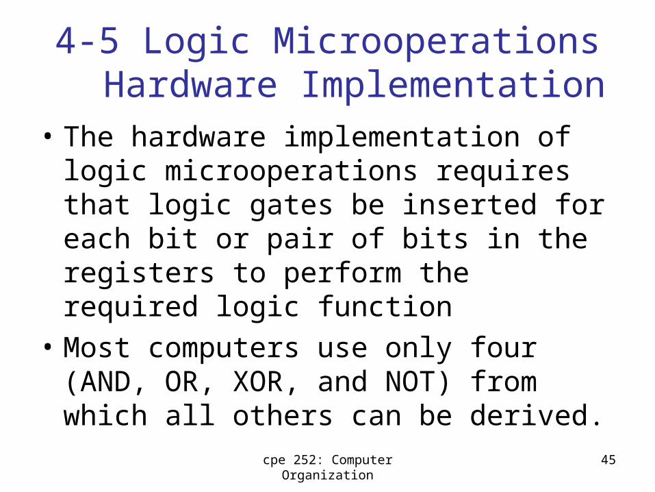
4-5 Logic MicrooperationsHardware Implementation
• The hardware implementation of logic microoperations requires that logic gates be inserted for each bit or pair of bits in the registers to perform the required logic function
• Most computers use only four (AND, OR, XOR, and NOT) from which all others can be derived.

cpe 252: Computer Organization 46
4-5 Logic MicrooperationsHardware Implementation cont.
S1
S0
0
1
2
3
4×1 MUX
Ei
Ai
Bi
S1 S0 OutputOperatio
n
0 0 E = A B XOR
0 1 E = A B OR
1 0 E = A B AND
1 1 E = A Complement
This is for one bit i
Figure B

cpe 252: Computer Organization 47
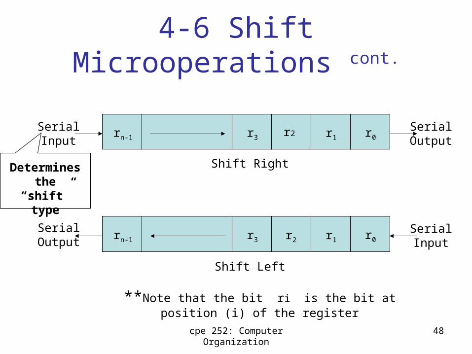
4-6 Shift Microoperations• Used for serial transfer of data• Also used in conjunction with arithmetic, logic,
and other data-processing operations• The contents of the register can be shifted to the
left or to the right• As being shifted, the first flip-flop receives its
binary information from the serial input• Three types of shift: Logical, Circular, and
Arithmetic
cpe 252: Computer Organization 48
4-6 Shift Microoperations cont.
r0r1r3rn-1
r0r1r2r3rn-1
Shift Right
Shift Left
Serial Input Serial Output
Serial Output Serial Input
Determines the “shift”
type
r2
**Note that the bit ri is the bit at position (i) of the register

cpe 252: Computer Organization 49
4-6 Shift Microoperations: Logical Shifts
• Transfers 0 through the serial input
• Logical Shift Right: R1←shr R1
• Logical Shift Left: R2←shl R2
The same
The same
Logical Shift Left
? 0r0r1r2r3rn-1

cpe 252: Computer Organization 50
4-6 Shift Microoperations: Circular Shifts (Rotate Operation)
• Circulates the bits of the register around the two ends without loss of information
• Circular Shift Right: R1←cir R1
• Circular Shift Left: R2←cil R2
The same
The same
Circular Shift Left
r0r1r2r3rn-1
cpe 252: Computer Organization 51
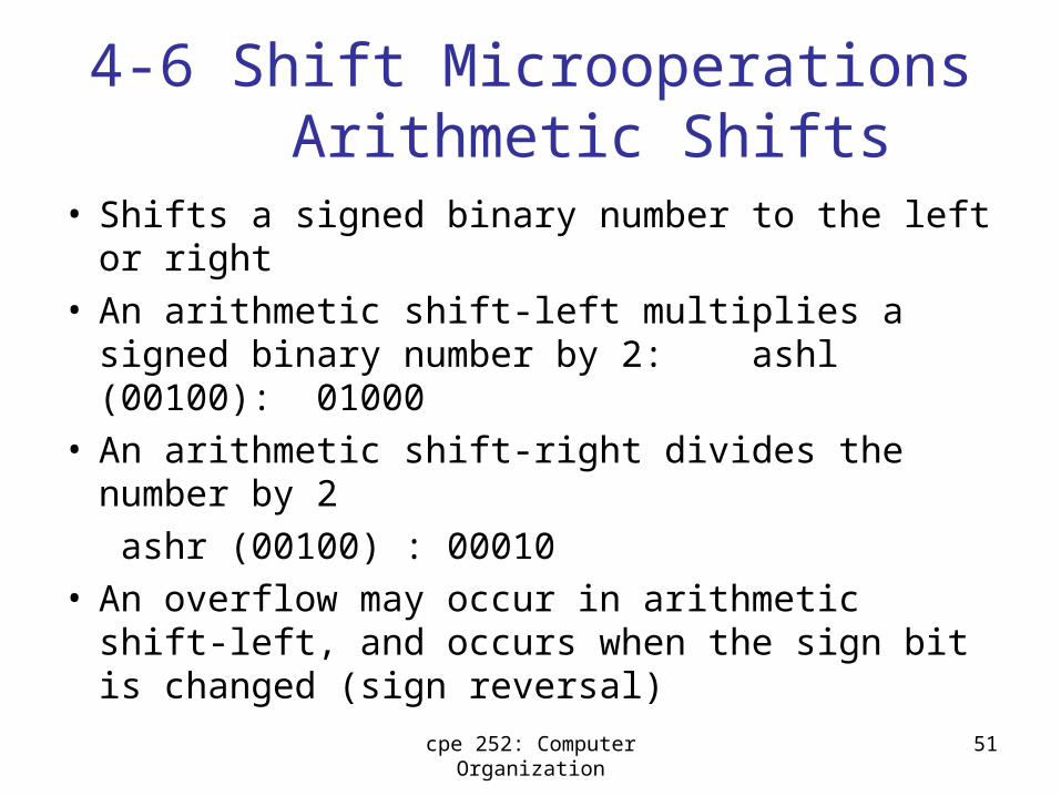
4-6 Shift Microoperations Arithmetic Shifts
• Shifts a signed binary number to the left or right• An arithmetic shift-left multiplies a signed binary
number by 2: ashl (00100): 01000• An arithmetic shift-right divides the number by 2
ashr (00100) : 00010• An overflow may occur in arithmetic shift-left,
and occurs when the sign bit is changed (sign reversal)

cpe 252: Computer Organization 52
4-6 Shift Microoperations Arithmetic Shifts cont.
Arithmetic Shift RightSign Bit
Arithmetic Shift LeftSign Bit
?
0?
r0r1r2r3rn-1
r0r1r2r3rn-1

cpe 252: Computer Organization 53
4-6 Shift Microoperations Arithmetic Shifts cont.
• An overflow flip-flop Vs can be used to detect an arithmetic shift-left overflow
Vs = Rn-1 Rn-2
Rn-2
Vs=Rn-1 1 overflow
0 no overflow
cpe 252: Computer Organization 54
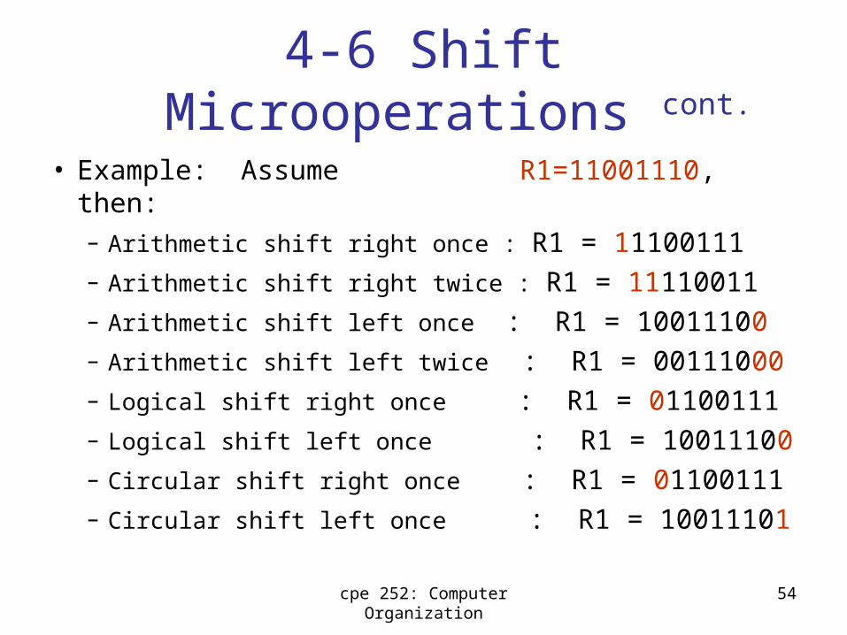
4-6 Shift Microoperations cont.
• Example: Assume R1=11001110, then:– Arithmetic shift right once : R1 = 11100111– Arithmetic shift right twice : R1 = 11110011– Arithmetic shift left once : R1 = 10011100– Arithmetic shift left twice : R1 = 00111000– Logical shift right once : R1 = 01100111– Logical shift left once : R1 = 10011100– Circular shift right once : R1 = 01100111– Circular shift left once : R1 = 10011101

cpe 252: Computer Organization 55
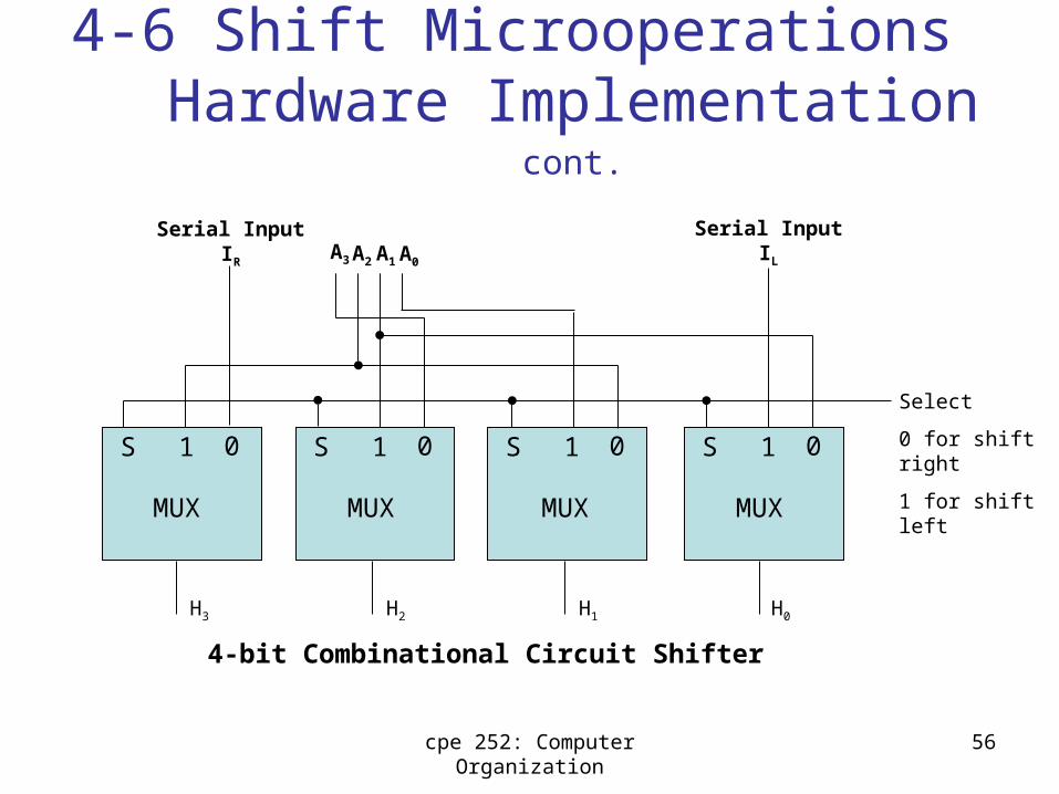
4-6 Shift Microoperations Hardware Implementation cont.
• A possible choice for a shift unit would be a bidirectional shift register with parallel load (refer to Fig 2-9). Has drawbacks:– Needs two pulses (the clock and the shift
signal pulse)– Not efficient in a processor unit where multiple
number of registers share a common bus
• It is more efficient to implement the shift operation with a combinational circuit
cpe 252: Computer Organization 56
4-6 Shift Microoperations Hardware Implementation cont.
S 1 0 S 1 0 S 1 0 S 1 0
A3A2 A1A0
Serial Input IR Serial Input IL
Select
0 for shift right
1 for shift left
H3 H2 H1 H0
MUX MUX MUX MUX
4-bit Combinational Circuit Shifter
cpe 252: Computer Organization 57
4-7 Arithmetic Logic Shift Unit
• Instead of having individual registers performing the microoperations directly, computer systems employ a number of storage registers connected to a common operational unit called an Arithmetic Logic Unit (ALU)

cpe 252: Computer Organization 58
4-7 Arithmetic Logic Shift Unit cont.
0123
S3
S2
S1
S0
Bi
Ai
Ai+1
Ai-1
Select
4×1 MUX
Ci
Ci+1
One stage of arithmetic
circuit (Fig.A)
One stage of logic circuit
(Fig.B)
Di
Ei
Fi
shrshl
One stage of ALU
Related Documents