LM5032 INTERLEAVED BOOST CONVERTER Abstract The LM5032 dual current mode PWM controller contains all the features needed to control an interleaved boost converter. The two outputs operate 180 degrees out of phase and have separate current limit inputs for each channel. In addition to a high input voltage range, the controller contains all the auxiliary features needed to control a complete converter. Introduction A basic boost converter converts a DC voltage to a higher DC voltage. Interleaving adds additional benefits such as reduced ripple currents in both the input and output circuits. Higher efficiency is realized by splitting the output current into two paths, substantially reducing I 2 R losses and inductor AC losses. Figure 1 shows the basic interleaved boost topology.

Welcome message from author
This document is posted to help you gain knowledge. Please leave a comment to let me know what you think about it! Share it to your friends and learn new things together.
Transcript
LM5032 INTERLEAVED BOOST CONVERTER
Abstract
The LM5032 dual current mode PWM controller contains all the features needed to control an interleaved boost converter. The two outputs operate 180 degrees out of phase and have separate current limit inputs for each channel. In addition to a high input voltage range, the controller contains all the auxiliary features needed to control a complete converter.
Introduction
A basic boost converter converts a DC voltage to a higher DC voltage. Interleaving adds additional benefits such as reduced ripple currents in both the input and output circuits. Higher efficiency is realized by splitting the output current into two paths, substantially reducing I2R losses and inductor AC losses. Figure 1 shows the basic interleaved boost topology.
Fig. 1 Interleaved Boost Basic Diagram
When Q1 turns on, current ramps up in L1 with a slope depending on the input voltage, storing energy in L1. D1 is off during this time since the output voltage is greater than the input voltage. Once Q1 turns off, D1 conducts delivering part of its stored energy to the load and the output capacitor. Current in L1 ramps down with a slope dependent on the difference between the input and output voltage. One half of a switching period later, Q2 also turns on completing the same cycle of events. Since both power channels are
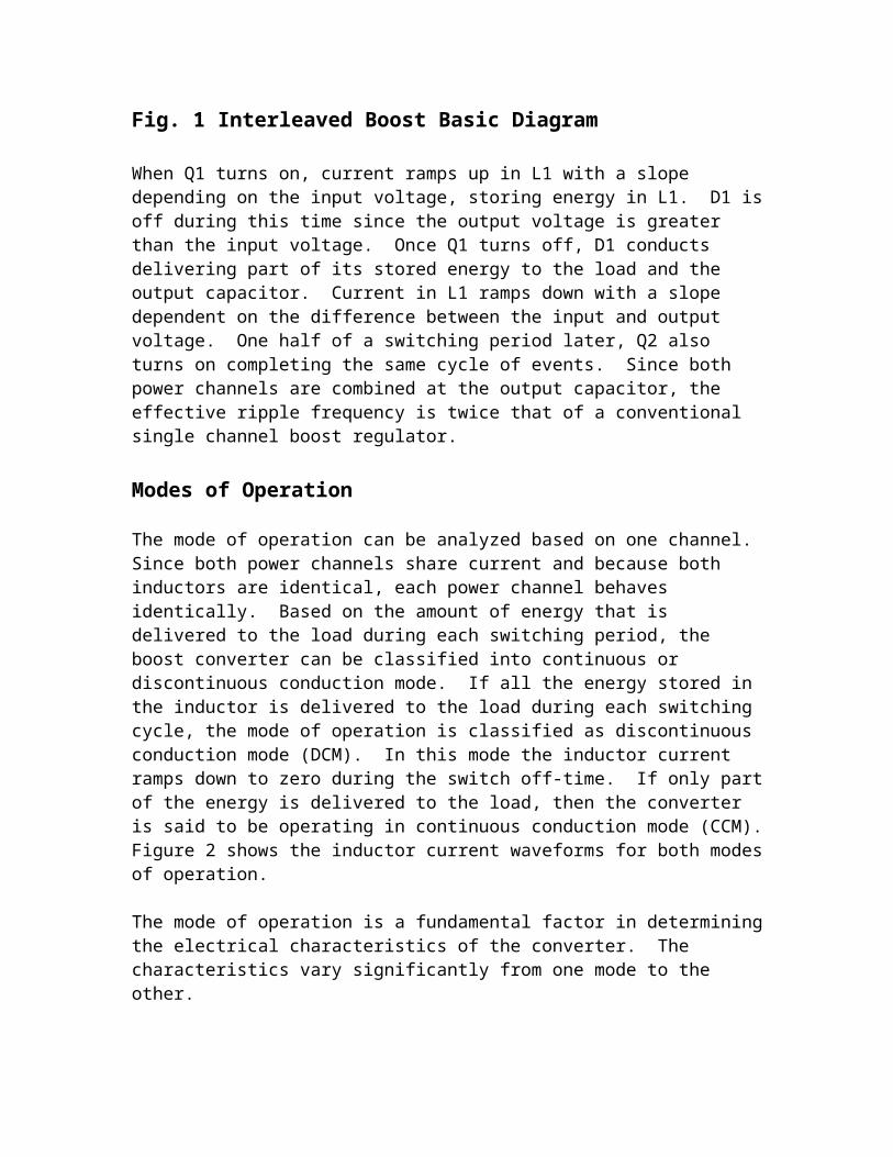
combined at the output capacitor, the effective ripple frequency is twice that of a conventional single channel boost regulator.
Modes of Operation
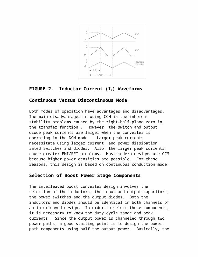
The mode of operation can be analyzed based on one channel. Since both power channels share current and because both inductors are identical, each power channel behaves identically. Based on the amount of energy that is delivered to the load during each switching period, the boost converter can be classified into continuous or discontinuous conduction mode. If all the energy stored in the inductor is delivered to the load during each switching cycle, the mode of operation is classified as discontinuous conduction mode (DCM). In this mode the inductor current ramps down to zero during the switch off-time. If only part of the energy is delivered to the load, then the converter is said to be operating in continuous conduction mode (CCM). Figure 2 shows the inductor current waveforms for both modes of operation.
The mode of operation is a fundamental factor in determining the electrical characteristics of the converter. The characteristics vary significantly from one mode to the other.
FIGURE 2. Inductor Current (IL) Waveforms
Continuous Versus Discontinuous Mode
Both modes of operation have advantages and disadvantages. The main disadvantages in using CCM is the inherent stability problems caused by the right-half-plane zero in the transfer function . However, the switch and output diode peak currents are larger when the converter is operating in the DCM mode. Larger peak currents necessitate using larger current and power dissipation rated switches and diodes. Also, the larger peak currents cause greater EMI/RFI problems. Most modern designs use CCM because higher power densities are possible. For these reasons, this design is based on continuous conduction mode.
Selection of Boost Power Stage Components
The interleaved boost converter design involves the selection of the inductors, the input and output capacitors, the power switches and the output diodes. Both the inductors and diodes should be identical in both channels of an interleaved design. In order to select these components, it is necessary to know the duty cycle range and peak currents. Since the output power is channeled through two power paths, a good starting point is to design the power path components using half the output power. Basically, the design starts with a single boost converter operating at half the power. However, a trade-off exists which will depend on the goals of the design. The designer may use smaller components since currents are smaller in each phase. Or, larger components may be selected to minimize losses. Specifically, this design uses the criteria of room temperature operation over the entire input voltage range without the requirement of airflow. Obviously, there are many trade-offs possible, such as requiring external airflow which would allow the use of smaller components and more power per watt.
Knowing the maximum and minimum input voltages, the output voltage, and the voltage drops across the output diode and switch, the maximum and minimum duty cycles are calculated. Next, the average inductor current can be estimated from the load current and duty cycle. Assuming the peak to peak inductor current ripple to be a certain percentage of the average inductor current, the peak inductor current can be estimated. The inductor value is then calculated using the ripple current, switching frequency, input voltage, and duty cycle information. Finally, the boundary between CCM and DCM is determined which will determine the minimum load current.
Once the inductor value has been chosen and the peak currents have been calculated, the other components may be selected. Selection of the input and output capacitors differ from a single phase design because of the reduced ripple and increased effective frequency.
Inductor Selection
(1)
(2)
Where VOUT is the output voltage, Vd is the forward voltage drop of the output diode, and V(ON) is the on stage voltage of the switching MOSFET. VIN(MAX) is the maximum input voltage, and VIN(MIN) is the minimum input voltage.
The average inductor current (maximum) per phase can be calculated knowing the output current, IOUT, remembering that the current per phase is one-half the total current. This is the origin of the 0.5 term in the numerator below.
(3)
As a starting point assume the peak inductor current ripple per phase, ΔIL to be a certain percentage of the average inductor current calculated in equation (3). A good starting value of ΔIL is about 40% or the output current which is 20% of the individual phase current. Inductor ripple will also determine the minimum output current for continuous mode operation, so some iteration may be necessary in choosing this parameter. The peak inductor current per phase is given by:
(4)
Knowing the switching frequency, fs the required inductance value per phase can be selected using:
(5)
At the boundary between CCM and DCM modes of operation, the peak inductor current per phase, IPEAK is the same as the peak to peak inductor current ripple per phase, ΔIL, as shown in Figure 2. Therefore, the average inductor current is at the boundary is given by:
(6)
From equations (3) and (6)
(7)
The critical value of the inductance per phase to maintain the converter in continuous mode related to output current is given by equations (5) and (7).
(8)
Knowing the minimum load current in a particular design L can be chosen. Obviously, there are trade-offs between minimum load current, percent ripple, and inductor size. Increasing the frequency helps in reducing inductor size.
Output Capacitor
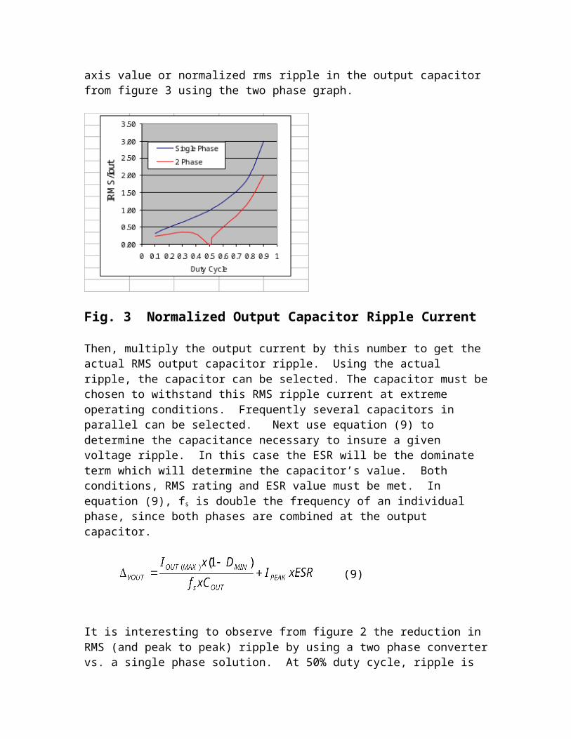
In a boost converter, the output capacitor must be chosen to withstand relatively high ripple current compared to an equivalent power buck regulator. The high ripple current flows through the equivalent series resistance (ESR) of the capacitor. ESR increases the capacitor temperature and increases ripple voltage. First calculate the worst case duty cycle for ripple which is usually the maximum duty cycle (refer to Fig. 3 for this value). Then read the y axis value or normalized rms ripple in the output capacitor from figure 3 using the two phase graph.
Fig. 3 Normalized Output Capacitor Ripple Current
Then, multiply the output current by this number to get the actual RMS output capacitor ripple. Using the actual ripple, the capacitor can be selected. The capacitor must be chosen to withstand this RMS ripple current at extreme operating conditions. Frequently several capacitors in parallel can be selected. Next use equation (9) to determine the capacitance necessary to insure a given voltage ripple. In this case the ESR will be the dominate term which will determine the capacitor’s value. Both conditions, RMS rating and ESR value must be met. In equation (9), fs is double the frequency of an individual phase, since both phases are combined at the output capacitor.
(9)
It is interesting to observe from figure 2 the reduction in RMS (and peak to peak) ripple by using a two phase converter vs. a single phase solution. At 50% duty cycle, ripple is nearly perfectly canceled, which occurs when VIN is twice VOUT.
Input Capacitor Selection
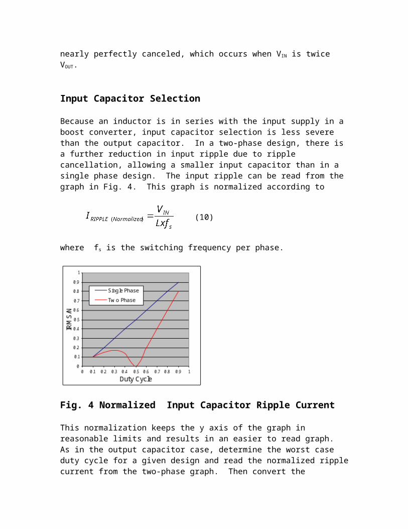
Because an inductor is in series with the input supply in a boost converter, input capacitor selection is less severe than the output capacitor. In a two-phase design, there is a further reduction in input ripple due to ripple cancellation, allowing a smaller input capacitor than in a single phase design. The input ripple can be read from the graph in Fig. 4. This graph is normalized according to
(10)
where fs is the switching frequency per phase.
Fig. 4 Normalized Input Capacitor Ripple Current
This normalization keeps the y axis of the graph in reasonable limits and results in an easier to read graph. As in the output capacitor case, determine the worst case duty cycle for a given design and read the normalized ripple current from the two-phase graph. Then convert the normalized ripple current to actual ripple current by multiplying by the normalization factor. Then size the input capacitor to handle this rms ripple value.
Power Switches Selection
Each MOSFET should be selected based on several parameters. The drain-source breakdown should be greater than the maximum input voltage plus some margin for ringing. The RDS(ON) value will determine conduction losses and must low enough to keep junction temperatures within specifications at the maximum drain current condition. Gate to source and gate to drain changes will contribute to AC losses. The thermal resistance rating will determine heatsink and airflow requirements. A more detailed calculation for the power dissipated in each MOSFET is given by:
(11)
The first term is the I2R term. The 1-D term in the denominator relates the output current to inductor current. The 2 in the denominator is necessary to get current per phase. The second term is the AC gate charge loss term with depends on phase frequency and the third term represents conduction switching loss.
Output Diode Selection
The output diode selection is based on voltage and current ratings, and reverse recovery time. The voltage rating should be VOUT plus some margin for ringing. VF should be as low as possible at the maximum output current specification to minimize conduction losses. Reverse recovery time trr should be as low as possible to minimize switching losses. Chose a Schottky rectifier if voltage ratings permit, otherwise an ultra-fast rectifier is required.
Compensation Components Selection
Compensation is similar to an equivalent power single phase boost regulator with the same inductor value. There is a right-half-plane zero in the continuous conduction mode which will influence loop bandwidth. A conservative approach is to insure the loop gain crosses zero at lower than 1/4th the switching (per phase) frequency. The frequency of the right-half-plane zero is given by
Prototype
A prototype was constructed using the LM5032 as the controller. The design goal was an interleaved converter with high efficiency and operation at full power without air or a heatsink at room temperature environment. Power was designed
around a limit of about 14 amps of input current, allowing the use of off the shelf surface mount inductors. Specifically, the specifications are:
VIN = 12 to 45 voltsVOUT = 48 volts IOUT = 4.5 ampsVRIPPLE-OUT < 50mV
Refer to Fig. 5 below for a complete schematic of the prototype.
Fig. 5 Schematic of Prototype
Figure1 shows the schematic of the prototype. The circuit is built around the LM5032, a 2 phase PWM controller with separate inputs for current limit and compensation for each channel. The separate inputs for the PWM comparator are combined in this design since we are implementing a two-phase, single output converter, not two independent converters. The two current limit inputs are used, since this insures current balance in each phase. Each output phase drives its own power channel consisting of switching FETs Q1 and Q2, Inductors L2 and L3, and output dual diode D2. The two power outputs are combined at the output capacitors C15-C19. The IC is internally configured to drive its two outputs 180 degrees out of phase.
A single feedback network consisting of error amplifier U4 and associated passive components drives both comp inputs which are tied together at the IC.
In order to reduce the sense resistor losses, a DC offset circuit was constructed to offset the current sense inputs by 185mV. This allowed the use of lower value

sense resistors in each phase, reducing I2R losses. The circuit of Fig.2 illustrates the DC offset circuit
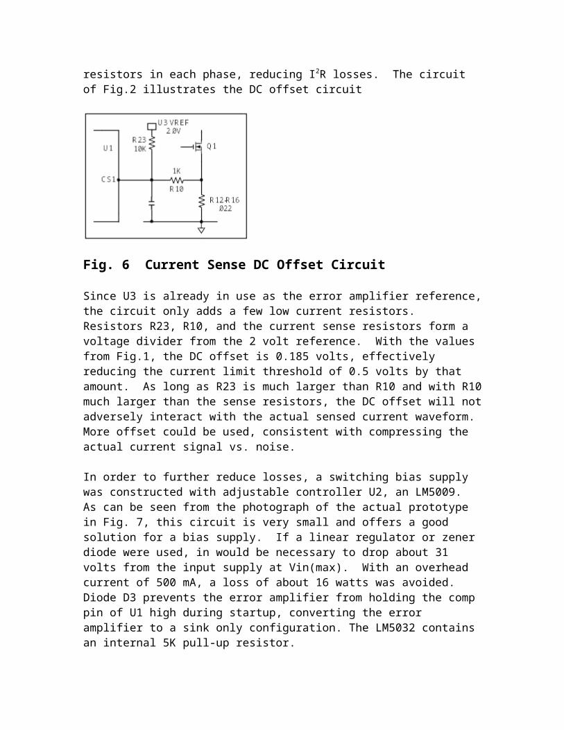
Fig. 6 Current Sense DC Offset Circuit
Since U3 is already in use as the error amplifier reference, the circuit only adds a few low current resistors. Resistors R23, R10, and the current sense resistors form a voltage divider from the 2 volt reference. With the values from Fig.1, the DC offset is 0.185 volts, effectively reducing the current limit threshold of 0.5 volts by that amount. As long as R23 is much larger than R10 and with R10 much larger than the sense resistors, the DC offset will not adversely interact with the actual sensed current waveform. More offset could be used, consistent with compressing the actual current signal vs. noise.
In order to further reduce losses, a switching bias supply was constructed with adjustable controller U2, an LM5009. As can be seen from the photograph of the actual prototype in Fig. 7, this circuit is very small and offers a good solution for a bias supply. If a linear regulator or zener diode were used, in would be necessary to drop about 31 volts from the input supply at Vin(max). With an overhead current of 500 mA, a loss of about 16 watts was avoided. Diode D3 prevents the error amplifier from holding the comp pin of U1 high during startup, converting the error amplifier to a sink only configuration. The LM5032 contains an internal 5K pull-up resistor.
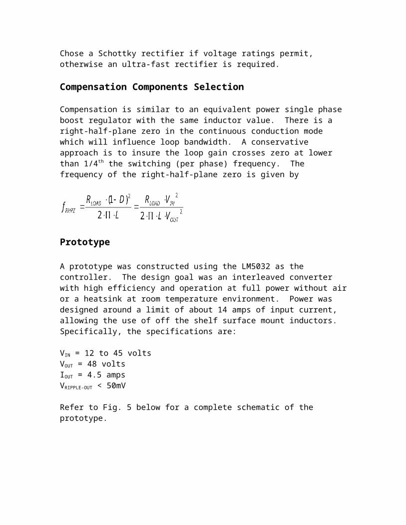
Fig. 7 Photographs of the Prototype
Referring the left photograph in Figure 3, the two power inductors occupy the top part of the left photograph, with rectification accomplished with the common cathode Schottky diode located just below the inductors. The LM5032 PWM controller is located in the lower left portion of the board. On the bottom side of the board the bias supply is located near the upper right, with the two switching FETs at center right. The error amplifier is located near the top left of the board. No heat-sinking other than the copper in the PCB is used. A four layer board was used for compactness of design and heat dissipation properties
Performance
Interleaved Boost Efficiency
80
82
84
86
88
90
92
94
96
98
100
0.10 0.50 0.90 1.30 1.70 2.10 2.50 2.90 3.30 3.70
Load (A)
Efficiency (%)
Vin=12VVin=24VVin=36VVin=42V
Fig. 8 Efficiency
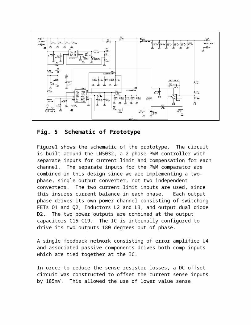
Fig. 9 Output Ripple
Referring to the plots in Fig. 4 taken at the DCM/CM boundary, efficiencies range from 95% to 98% up to the full 4 amps of output current, and over a 3.5:1 input voltage range. The very low current region where overhead bias currents dominate does have less efficiency, but this is true of all regulators. These plots illustrate the possibility of building a compact, high power boost converter without sacrificing excellent efficiency
Input and output ripple reduction are some of the benefits of an interleaved converter. Since the output ripple is double the frequency of the individual phases and at a lower RMS current value, the designer has the choice of smaller output capacitors with the same ripple as a single phase converter, or using larger capacitors to achieve even lower output ripple. Effective ripple is a function of duty cycle. Figures 3 and 4 illustrates the input and output ripple currents vs. duty cycle relationships. Fig. 9 shows the output ripple of the prototype which is less than the 50mV target. Since ripple reduction is a function of duty cycle, the degree of ripple overlap is also a function of duty cycle. There is near perfect cancellation of ripple at 50% duty cycle. This opens the intriguing possibility of building a converter with little to no output ripple if the designer can limit Vin to the proper value for 50% duty cycle. In the more general case, ripple is reduced by as much as 50% compared to an equivalent power single phase converter. Likewise, inductor selection is flexible with the two phase design. One-half the single phase inductor value can be chosen, which will make each inductor smaller, but results in the same ripple currents as the single phase design. Or the inductors can remain the same value as in the single phase
design, reducing the ripple by one-half. The proper trade-offs will depend on the overall design goal. Attention to ESR requirements will keep capacitors within temperature ratings and the output voltage ripple within specifications.
Table 1. BOM
Related Documents