1 ESE 570: Digital Integrated Circuits and VLSI Fundamentals Lec 19: March 30, 2017 Dynamic Logic, Charge Injection Penn ESE 570 Spring 2017 – Khanna Lecture Outline ! Review: Sequential MOS Logic " D-Latch ! Dynamic Logic " Domino Logic ! Charge Leakage ! Charge Sharing ! Domino Logic Design Considerations ! Logic Comparisons 2 Penn ESE 570 Spring 2017 – Khanna Latch Design Penn ESE 570 Spring 2017 - Khanna 3 Latch Design Penn ESE 570 Spring 2017 - Khanna 4 Latch Design Penn ESE 570 Spring 2017 - Khanna 5 Latch Design Penn ESE 570 Spring 2017 - Khanna 6

Welcome message from author
This document is posted to help you gain knowledge. Please leave a comment to let me know what you think about it! Share it to your friends and learn new things together.
Transcript
1
ESE 570: Digital Integrated Circuits and VLSI Fundamentals
Lec 19: March 30, 2017 Dynamic Logic, Charge Injection
Penn ESE 570 Spring 2017 – Khanna
Lecture Outline
! Review: Sequential MOS Logic " D-Latch
! Dynamic Logic " Domino Logic
! Charge Leakage ! Charge Sharing ! Domino Logic Design Considerations ! Logic Comparisons
2 Penn ESE 570 Spring 2017 – Khanna
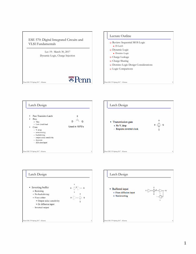
Latch Design
Penn ESE 570 Spring 2017 - Khanna 3
Latch Design
Penn ESE 570 Spring 2017 - Khanna 4
Latch Design
Penn ESE 570 Spring 2017 - Khanna 5
Latch Design
Penn ESE 570 Spring 2017 - Khanna 6
2
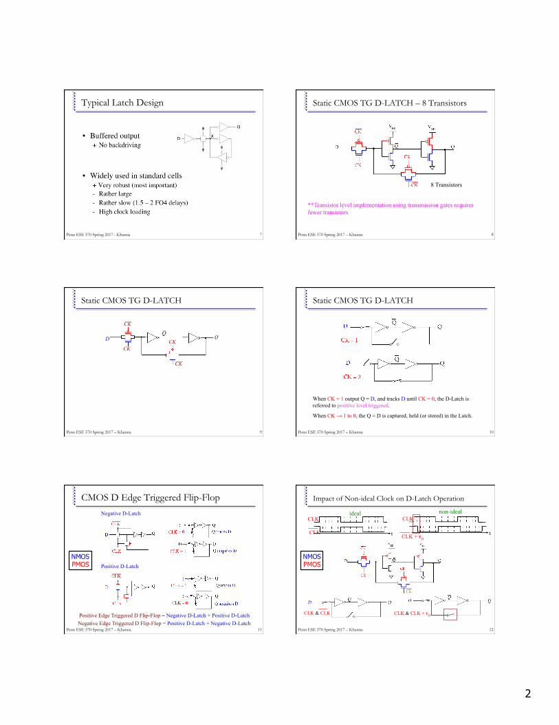
Typical Latch Design
Penn ESE 570 Spring 2017 - Khanna 7
Static CMOS TG D-LATCH – 8 Transistors
8
**Transistor level implementation using transmission gates requires fewer transistors
8 Transistors
Penn ESE 570 Spring 2017 – Khanna
9
D
CKCK
CK
CK
Static CMOS TG D-LATCH
Penn ESE 570 Spring 2017 – Khanna
10
Static CMOS TG D-LATCH
When CK = 1 output Q = D, and tracks D until CK = 0, the D-Latch is referred to positive level triggered.
When CK → 1 to 0, the Q = D is captured, held (or stored) in the Latch.
Penn ESE 570 Spring 2017 – Khanna
CMOS D Edge Triggered Flip-Flop
11
Positive Edge Triggered D Flip-Flop = Negative D-Latch + Positive D-Latch Negative Edge Triggered D Flip-Flop = Positive D-Latch + Negative D-Latch
Positive D-Latch
Negative D-Latch
NMOS PMOS
Penn ESE 570 Spring 2017 – Khanna
Impact of Non-ideal Clock on D-Latch Operation
12
CLK
CLK
CLK ideal non-ideal
CLK & CLK
CLK + τD
CLK & CLK + τD
t t
NMOS PMOS
Penn ESE 570 Spring 2017 – Khanna
3
t
t
ϕ1
ϕ2
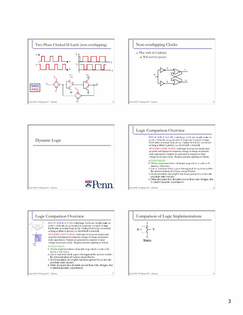
Two-Phase Clocked D-Latch (non-overlapping)
13 ϕ2
ϕ1
ϕ1
ϕ2
ϕ1
ϕ2
NMOS PMOS
Penn ESE 570 Spring 2017 – Khanna
Non-overlapping Clocks
! Play with in Cadence " Will need for project
Penn ESE 570 Spring 2017 - Khanna 14
Dynamic Logic
15 Penn ESE 570 Spring 2017 – Khanna
Logic Comparison Overview
16 Penn ESE 570 Spring 2017 – Khanna
DYNAMIC LOGIC GATES: valid logic level are not steady-state op points and depend on temporary storage of charge on parasitic node capacitances. Outputs are generated in response to input voltage levels and a clock. Requires periodic updating or refresh.
Logic Comparison Overview
17 Penn ESE 570 Spring 2017 – Khanna
DYNAMIC LOGIC GATES: valid logic level are not steady-state op points and depend on temporary storage of charge on parasitic node capacitances. Outputs are generated in response to input voltage levels and a clock. Requires periodic updating or refresh.
CSM1
BL
WL
CBL
WL
X
BL
VDD−VT
VDD/2
VDD
GND
Write "1" Read "1"
sensingVDD/2
ΔV VBL VPRE– VBIT VPRE–( )CS
CS CBL+------------------------= =
Write: CS is charged or discharged by asserting WL and BL.Read: Charge redistribution takes places between bit line and storage capacitance
Voltage swing is small; typically around 250 mV.
bit bit_b
N1
N2P1
A
P2
N3
N4
A_b
word
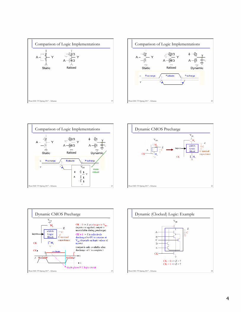
Comparison of Logic Implementations
18
Y
Ratioed
Penn ESE 570 Spring 2017 – Khanna
4
Comparison of Logic Implementations
19
Y
Ratioed
Penn ESE 570 Spring 2017 – Khanna
Comparison of Logic Implementations
20
Y
Ratioed
Penn ESE 570 Spring 2017 – Khanna
Comparison of Logic Implementations
21
Y
Ratioed
1
1
1
VDD more robust
Penn ESE 570 Spring 2017 – Khanna
Dynamic CMOS Precharge
22
VDD
A
CK
Mp
Me
Z
Penn ESE 570 Spring 2017 – Khanna
Dynamic CMOS Precharge
23
Z
Z
of C is complete
Penn ESE 570 Spring 2017 – Khanna
Dynamic (Clocked) Logic: Example
24
CK = 0 => Z = ? CK = 1 => Z = ?
Penn ESE 570 Spring 2017 – Khanna
5
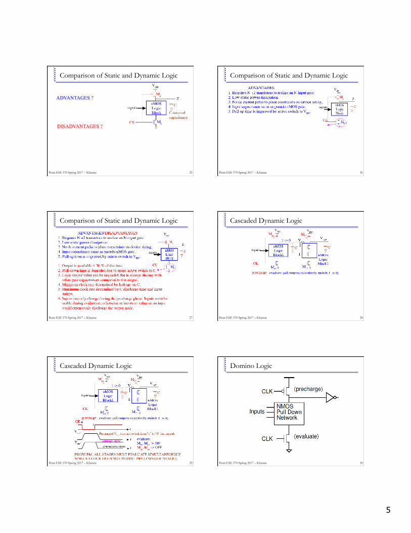
Comparison of Static and Dynamic Logic
25
ADVANTAGES ?
DISADVANTAGES ?
Penn ESE 570 Spring 2017 – Khanna
26
Comparison of Static and Dynamic Logic
Penn ESE 570 Spring 2017 – Khanna
27
Comparison of Static and Dynamic Logic
Penn ESE 570 Spring 2017 – Khanna
Cascaded Dynamic Logic
28 Penn ESE 570 Spring 2017 – Khanna
Cascaded Dynamic Logic
29 Penn ESE 570 Spring 2017 – Khanna
Domino Logic
30 Penn ESE 570 Spring 2017 – Khanna
6
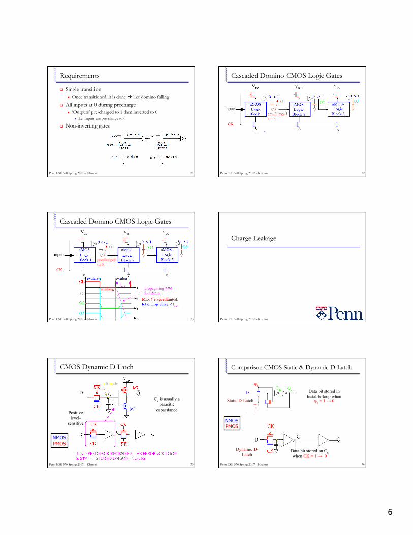
Requirements
! Single transition " Once transitioned, it is done # like domino falling
! All inputs at 0 during precharge " ‘Outputs’ pre-charged to 1 then inverted to 0
" I.e. Inputs are pre-charge to 0
! Non-inverting gates
31 Penn ESE 570 Spring 2017 – Khanna
Cascaded Domino CMOS Logic Gates
32 Penn ESE 570 Spring 2017 – Khanna
Cascaded Domino CMOS Logic Gates
33
propagating
Penn ESE 570 Spring 2017 – Khanna
Charge Leakage
Penn ESE 570 Spring 2017 – Khanna
CMOS Dynamic D Latch
35
Kenneth R. Laker, University of Pennsylvania,
updated 25Mar15
Cx is usually a parasitic
capacitance Positive level-
sensitive
D Q
NMOS PMOS
Penn ESE 570 Spring 2017 – Khanna
Comparison CMOS Static & Dynamic D-Latch
36
Kenneth R. Laker, University of Pennsylvania,
updated 25Mar15
Data bit stored on Cx when CK = 1 → 0
Dynamic D-Latch
ϕ1
ϕ1
Static D-Latch
Data bit stored in bistable-loop when
ϕ1 = 1 → 0
NMOS PMOS
Penn ESE 570 Spring 2017 – Khanna
7
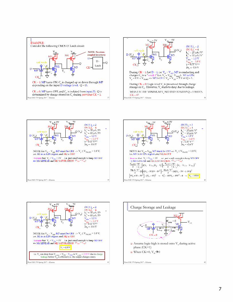
Penn ESE 570 Spring 2017 – Khanna
37
Kenneth R. Laker, University of Pennsylvania,
updated 25Mar15
NOTE: No cross-coupled inverters)
Flip-Flop
Latch circuit:
Latch
Penn ESE 570 Spring 2017 – Khanna
38
Kenneth R. Laker, University of Pennsylvania,
updated 25Mar15
Penn ESE 570 Spring 2017 – Khanna
39
Kenneth R. Laker, University of Pennsylvania,
updated 25Mar15
Vy = VT0n = 1V (VGD > VT0p)
Vy ≤ VT0n,M3 = 1.0 V;
Penn ESE 570 Spring 2017 – Khanna
40
Kenneth R. Laker, University of Pennsylvania,
updated 25Mar15
Vy = VT0n = 1V (VGD > VT0p)
Vy ≤ VT0n,M3 = 1.0 V;
Penn ESE 570 Spring 2017 – Khanna
41
Kenneth R. Laker, University of Pennsylvania,
updated 25Mar15
Vy = VT0n = 1V (VGD > VT0p)
Vy ≤ VT0n,M3 = 1.0 V;
i.e. Vx can drop from Vx-max = VDD – VTMP to Vx-min = 2.55 V due to charge leakage before VQ is effected (i.e. the output changes state).
Charge Storage and Leakage
! Assume logic-high is stored onto Vx during active phase (CK=1)
! When CK=0, Vin#0
42 Penn ESE 570 Spring 2017 – Khanna
8
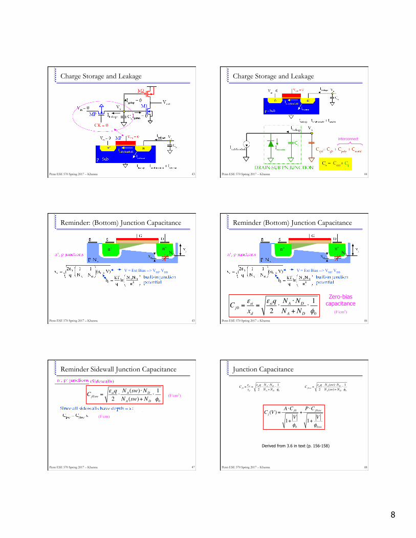
Charge Storage and Leakage
43 Penn ESE 570 Spring 2017 – Khanna
44
Cext
Cext
Charge Storage and Leakage
interconnect
Penn ESE 570 Spring 2017 – Khanna
Reminder: (Bottom) Junction Capacitance
45 Penn ESE 570 Spring 2017 – Khanna
V = Ext Bias --> VSB, VDB +
n+ n+ ND
46 Penn ESE 570 Spring 2017 – Khanna
V = Ext Bias --> VSB, VDB +
n+ n+ ND
Cj0 =εsixd=
εsiq2⋅NA ⋅ND
NA + ND
⋅1φ0
Zero-bias capacitance
(F/cm2)
Reminder (Bottom) Junction Capacitance
Reminder Sidewall Junction Capacitance
47
(F/cm2)
(F/cm)
Cj0sw =εsiq2⋅NA (sw) ⋅ND
NA (sw)+ ND
⋅1φ0
Penn ESE 570 Spring 2017 – Khanna
Junction Capacitance
48
Cj0sw =εsiq2⋅NA (sw) ⋅ND
NA (sw)+ ND
⋅1φ0
Cj0 =εsixd=
εsiq2⋅NA ⋅ND
NA + ND
⋅1φ0
Cj (V ) =A ⋅Cj0
1+Vφ0
+P ⋅Cj0sw
1+Vφ0sw
Derived from 3.6 in text (p. 156-158)
Penn ESE 570 Spring 2017 – Khanna
9
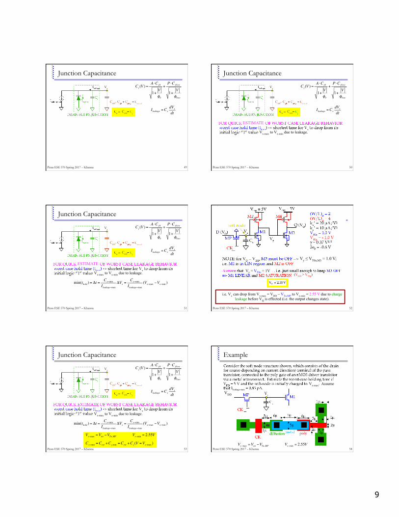
Junction Capacitance
49
Cext
Cext
Cj (V ) =A ⋅Cj0
1+Vφ0
+P ⋅Cj0sw
1+Vφ0sw
Ileakage =CxdVxdt
Penn ESE 570 Spring 2017 – Khanna
Junction Capacitance
50
Cext
Cext
Cj (V ) =A ⋅Cj0
1+Vφ0
+P ⋅Cj0sw
1+Vφ0sw
Ileakage =CxdVxdt
Vx-max to Vx-min due to leakage.
Penn ESE 570 Spring 2017 – Khanna
ESTIMATE
Junction Capacitance
51
Cext
Cext
Cj (V ) =A ⋅Cj0
1+Vφ0
+P ⋅Cj0sw
1+Vφ0sw
Ileakage =CxdVxdt
Vx-max to Vx-min due to leakage.
min(thold ) = Δt =Cx−min
Ileakage−maxΔVx =
Cx−min
Ileakage−max(Vx−max −Vx−min )
Penn ESE 570 Spring 2017 – Khanna
ESTIMATE
Penn ESE 570 Spring 2017 – Khanna
52
Kenneth R. Laker, University of Pennsylvania,
updated 25Mar15
Vy = VT0n = 1V (VGD > VT0p)
Vy ≤ VT0n,M3 = 1.0 V;
i.e. Vx can drop from Vx-max = VDD – VTn,MP to Vx-min = 2.55 V due to charge leakage before VQ is effected (i.e. the output changes state).
Junction Capacitance
53
Cext
Cext
Cj (V ) =A ⋅Cj0
1+Vφ0
+P ⋅Cj0sw
1+Vφ0sw
Ileakage =CxdVxdt
Vx-max to Vx-min due to leakage.
min(thold ) = Δt =Cx−min
Ileakage−maxΔVx =
Cx−min
Ileakage−max(Vx−max −Vx−min )
Vx−max =VDD −VTn,MP Vx−min = 2.55V
Cx−min =Cext +Cj,min =Cext +Cj (V =Vx−max )Penn ESE 570 Spring 2017 – Khanna
Example
54
Kenneth R. Laker, University of Pennsylvania,
updated 25Mar15
Vx-max. Assume
VDD
leakage-max
Vx−max =VDD −VTn,MP Vx−min = 2.55VPenn ESE 570 Spring 2017 – Khanna
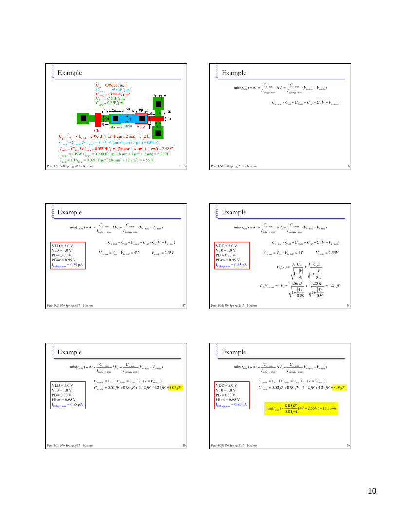
10
Example
55
Cn+p+ = CJSW Pn+p+ = 0.200 fF/µm (18 µm + 6 µm + 2 µm) = 5.20 fF Cn+p = CJ An+p = 0.095 fF/µm2 (36 µm2 + 12 µm2) = 4.56 fF
Penn ESE 570 Spring 2017 – Khanna
Example
56
min(thold ) = Δt =Cx−min
Ileakage−maxΔVx =
Cx−min
Ileakage−max(Vx−max −Vx−min )
Cx−min =Cext +Cj,min =Cext +Cj (V =Vx−max )
Penn ESE 570 Spring 2017 – Khanna
Example
57
min(thold ) = Δt =Cx−min
Ileakage−maxΔVx =
Cx−min
Ileakage−max(Vx−max −Vx−min )
Cx−min =Cext +Cj,min =Cext +Cj (V =Vx−max )
Vx−max =VDD −VTn,MP ≈ 4V Vx−min = 2.55V
VDD = 5.0 V VT0 = 1.0 V PB = 0.88 V PBsw = 0.95 V Ileakage,max = 0.85 pA
Penn ESE 570 Spring 2017 – Khanna
Example
58
min(thold ) = Δt =Cx−min
Ileakage−maxΔVx =
Cx−min
Ileakage−max(Vx−max −Vx−min )
Cx−min =Cext +Cj,min =Cext +Cj (V =Vx−max )
Vx−max =VDD −VTn,MP ≈ 4V Vx−min = 2.55V
Cj (V ) =A ⋅Cj0
1+Vφ0
+P ⋅Cj0sw
1+Vφ0sw
Cj (Vx−max = 4V ) =4.56 fF
1+4V0.88
+5.20 fF
1+4V0.95
= 4.21 fF
VDD = 5.0 V VT0 = 1.0 V PB = 0.88 V PBsw = 0.95 V Ileakage,max = 0.85 pA
Penn ESE 570 Spring 2017 – Khanna
Example
59
min(thold ) = Δt =Cx−min
Ileakage−maxΔVx =
Cx−min
Ileakage−max(Vx−max −Vx−min )
Cx−min =Cext +Cj,min =Cext +Cj (V =Vx−max )Cx−min = 0.52 fF + 0.90 fF + 2.42 fF + 4.21 fF = 8.05 fF
VDD = 5.0 V VT0 = 1.0 V PB = 0.88 V PBsw = 0.95 V Ileakage,max = 0.85 pA
Penn ESE 570 Spring 2017 – Khanna
Example
60
min(thold ) = Δt =Cx−min
Ileakage−maxΔVx =
Cx−min
Ileakage−max(Vx−max −Vx−min )
Cx−min =Cext +Cj,min =Cext +Cj (V =Vx−max )Cx−min = 0.52 fF + 0.90 fF + 2.42 fF + 4.21 fF = 8.05 fF
VDD = 5.0 V VT0 = 1.0 V PB = 0.88 V PBsw = 0.95 V Ileakage,max = 0.85 pA
min(thold ) =8.05 fF0.85pA
(4V − 2.55V ) =13.73ms
Penn ESE 570 Spring 2017 – Khanna
11
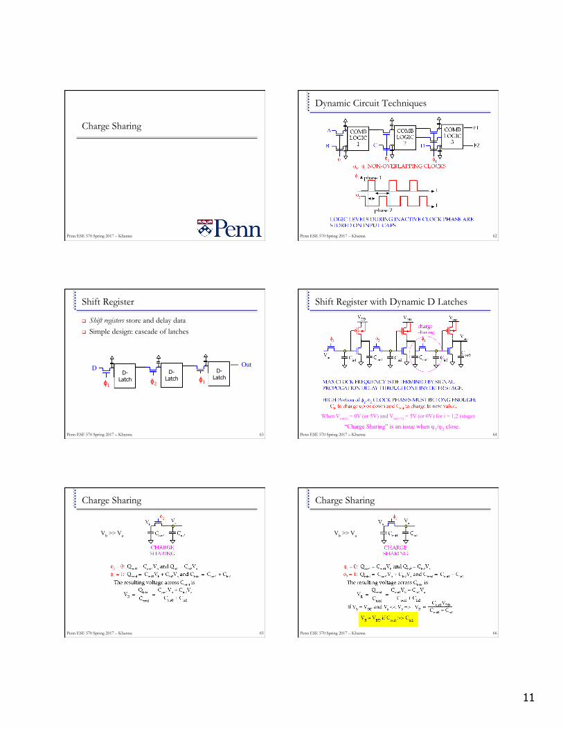
Charge Sharing
Penn ESE 570 Spring 2017 – Khanna
Dynamic Circuit Techniques
62
Kenneth R. Laker, University of Pennsylvania,
updated 25Mar15
Penn ESE 570 Spring 2017 – Khanna
Shift Register
! Shift registers store and delay data ! Simple design: cascade of latches
63
DD-
Latch D-
Latch D-
Latch
Out
ϕ1 ϕ1 ϕ2
Penn ESE 570 Spring 2017 – Khanna
Shift Register with Dynamic D Latches
64
Kenneth R. Laker, University of Pennsylvania,
updated 25Mar15
When Vout(i) = 0V (or 5V) and Vin(i+1) = 5V (or 0V) for i = 1,2 (stage)
“Charge Sharing” is an issue when ϕ1/ϕ2 close. Penn ESE 570 Spring 2017 – Khanna
Charge Sharing
65
Kenneth R. Laker, University of Pennsylvania,
updated 25Mar15
Vb >> Va
Penn ESE 570 Spring 2017 – Khanna
Charge Sharing
66
Kenneth R. Laker, University of Pennsylvania,
updated 25Mar15
Vb >> Va
Penn ESE 570 Spring 2017 – Khanna
12
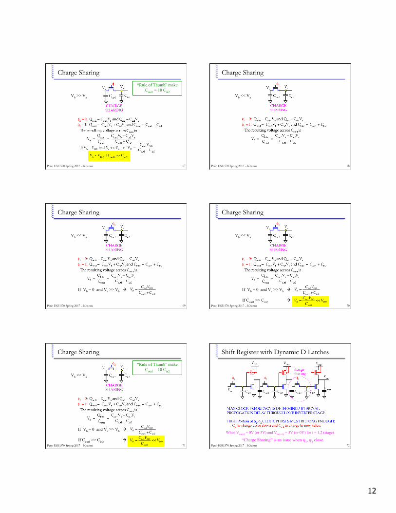
Charge Sharing
67
Kenneth R. Laker, University of Pennsylvania,
updated 25Mar15
“Rule of Thumb” make Cout1 = 10 Cin2
Vb >> Va
Penn ESE 570 Spring 2017 – Khanna
Charge Sharing
68
Kenneth R. Laker, University of Pennsylvania,
updated 25Mar15
Vb << Va
Penn ESE 570 Spring 2017 – Khanna
Charge Sharing
69
Kenneth R. Laker, University of Pennsylvania,
updated 25Mar15
Vb << Va
If Vb = 0 and Va >> Vb # VR ≈Cin2VDDCout1 +Cin2
Penn ESE 570 Spring 2017 – Khanna
Charge Sharing
70
Kenneth R. Laker, University of Pennsylvania,
updated 25Mar15
Vb << Va
If Vb = 0 and Va >> Vb # VR ≈Cin2VDDCout1 +Cin2
If Cout1 >> Cin2 # VR ≈Cin2VDDCout1
<<VDDPenn ESE 570 Spring 2017 – Khanna
Charge Sharing
71
Kenneth R. Laker, University of Pennsylvania,
updated 25Mar15
“Rule of Thumb” make Cout1 = 10 Cin2
Vb << Va
If Vb = 0 and Va >> Vb # VR ≈Cin2VDDCout1 +Cin2
If Cout1 >> Cin2 # VR ≈Cin2VDDCout1
<<VDDPenn ESE 570 Spring 2017 – Khanna
Shift Register with Dynamic D Latches
72
Kenneth R. Laker, University of Pennsylvania,
updated 25Mar15
When Vout(i) = 0V (or 5V) and Vin(i+1) = 5V (or 0V) for i = 1,2 (stage)
“Charge Sharing” is an issue when ϕ1, ϕ2 close. Penn ESE 570 Spring 2017 – Khanna
13
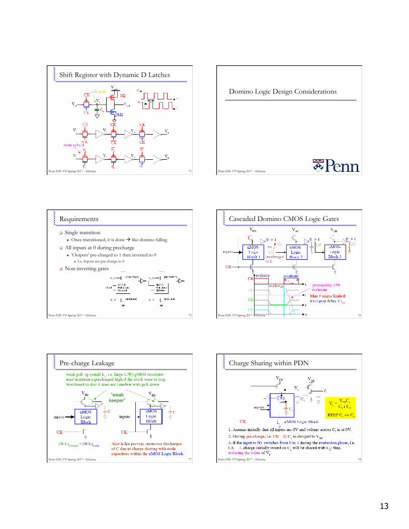
73
Kenneth R. Laker, University of Pennsylvania,
updated 25Mar15
m
Shift Register with Dynamic D Latches
Penn ESE 570 Spring 2017 – Khanna
Domino Logic Design Considerations
Penn ESE 570 Spring 2017 – Khanna
Requirements
! Single transition " Once transitioned, it is done # like domino falling
! All inputs at 0 during precharge " ‘Outputs’ pre-charged to 1 then inverted to 0
" I.e. Inputs are pre-charge to 0
! Non-inverting gates
75 Penn ESE 570 Spring 2017 – Khanna
Cascaded Domino CMOS Logic Gates
76
Kenneth R. Laker, University of Pennsylvania,
updated 25Mar15
propagating
Penn ESE 570 Spring 2017 – Khanna
Pre-charge Leakage
77
Kenneth R. Laker, University of Pennsylvania,
updated 25Mar15
“weak keeper”
(W/L)p-keeper < (W/L)n-min
Penn ESE 570 Spring 2017 – Khanna
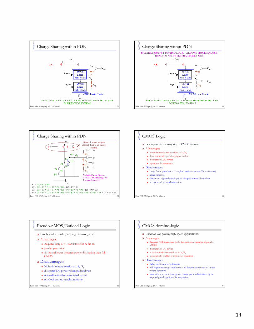
Charge Sharing within PDN
78
Kenneth R. Laker, University of Pennsylvania,
updated 25Mar15
Penn ESE 570 Spring 2017 – Khanna
14
79
Kenneth R. Laker, University of Pennsylvania,
updated 25Mar15
Charge Sharing within PDN
Penn ESE 570 Spring 2017 – Khanna
80
Kenneth R. Laker, University of Pennsylvania,
updated 25Mar15
Charge Sharing within PDN
Penn ESE 570 Spring 2017 – Khanna
81
Since all nodes are pre-charged there is no charge-
sharing.
C4
C3
C2
C1
Z4
Z3
Z2
Z1
P0
Z1 = G1 + P1 * P0 Z2 = G2 + P2 * G1 + P2 * P1 * P0 = G2 + P2 * Z1 Z3 = G3 + P3 * G2 + P3 * P2 * G1 + P3 * P2 * P1 * P0 = G3 + P3 * Z2 Z4 = G4 + P4 * G3 + P4 * P3 * G2 + P4 * P3 * P2 * G1 + P4 * P3 *P1 * P0 = G4 + P4 * Z3
Charge Sharing within PDN
Penn ESE 570 Spring 2017 – Khanna
CMOS Logic
! Best option in the majority of CMOS circuits ! Advantages:
" Noise-immunity not sensitive to kn/kp
" does not involve pre-charging of nodes " dissipates no DC power " layout can be automated
! Disadvantages: " Large fan-in gates lead to complex circuit structures (2N transistors) " larger parasitics " slower and higher dynamic power dissipation than alternatives " no clock and no synchronization.
82 Penn ESE 570 Spring 2017 – Khanna
Pseudo-nMOS/Ratioed Logic
! Finds widest utility in large fan-in gates ! Advantages:
" Requires only N+1 transistors for N fan-in " smaller parasitics " faster and lower dynamic power dissipation than full
CMOS
! Disadvantages: " Noise-immunity sensitive to kn/kp
" dissipates DC power when pulled down " not well-suited for automated layout " no clock and no synchronization.
83 Penn ESE 570 Spring 2017 – Khanna
CMOS domino-logic
! Used for low-power, high-speed applications. ! Advantages:
" Requires N+k transistors for N fan-in (size advantages of pseudo-nMOS)
" dissipates no DC power " noise immunity not sensitive to kn/kp " use of clocks enables synchronous operation
! Disadvantages: " Relies on storage on soft nodes " will require thorough simulation at all the process corners to insure
proper operation " some of the speed advantage over static gates is diminished by the
required pre-charge (pre-discharge) time
84 Penn ESE 570 Spring 2017 – Khanna
15
Ideas
! Leads to clocked circuit discipline " Uses state holding element (eg. Latches and registers) " Prevents timing assumptions and complex reasoning about all possible
timings
! Dynamic/clocked logic " Only build/drive one pulldown network " Fast transition propagation
! Domino Logic allows for cascading ! Charge Leakage
" Constrains maximum clock frequency
! Charge Sharing with pass gates " Need to size carefully
! Different logic-types for different applications
85 Penn ESE 570 Spring 2017 – Khanna
Admin
! HW 7 out now " Due 4/6 @ midnight " EC due 4/9 @ midnight
! Start getting groups together for project " Groups of 2 " Names due by 4/6 " Use piazza to find partners
86 Penn ESE 570 Spring 2017 – Khanna
Related Documents