Laboratory Exercises to accompany David G. Alciatore Department of Mechanical Engineering Colorado State University 2019 Edition This is not Copyrighted material. Feel free to print and distribute this document. For more information, please refer to the book website at: mechatronics.colostate.edu and for video demonstrations, see the Lab book website at: mechatronics.colostate.edu/lab_book.html

Welcome message from author
This document is posted to help you gain knowledge. Please leave a comment to let me know what you think about it! Share it to your friends and learn new things together.
Transcript

Laboratory Exercises
to accompany
David G. Alciatore
Department of Mechanical EngineeringColorado State University
2019 Edition
This is not Copyrighted material.Feel free to print and distribute this document.
For more information, please refer to the book website at:mechatronics.colostate.edu
and for video demonstrations, see the Lab book website at:mechatronics.colostate.edu/lab_book.html


Table of Contents
General Equipment List 5
Laboratory 1Introduction - Resistor Codes, Breadboard, and Basic Measurements 9
Laboratory 2Instrument Familiarization and Basic Electrical Relations 19
Laboratory 3The Oscilloscope 37
Laboratory 4Bandwidth, Filters, and Diodes 59
Laboratory 5Transistor and Photoelectric Circuits 73
Laboratory 6Operational Amplifier Circuits 83
Laboratory 7Digital Circuits - Logic and Latching 95
Laboratory 8Digital Circuits - Counter and LED Display 107
Laboratory 9Programming a PIC Microcontroller - Part I 121
Laboratory 10Programming a PIC Microcontroller - Part II 141
Laboratory 11Pulse-Width-Modulation Motor Speed Control with a PIC 155
Laboratory 12Data Acquisition 171
Laboratory 13Strain Gages 187
Laboratory 14Vibration Measurement With an Accelerometer 197
Laboratory 15Practical Advice for Microcontroller-based Design Projects 203


5
General Equipment and Supplies List
Where possible, the exercises in this book were developed so they could apply in any Lab setting, with any equipment (even virtual PC-based instrumentation). However, for refer-ence, all equipment used in the Lab at CSU are summarized below.
Recommended Equipment and Software:• NI Elvis II+
• HP 54602A Oscilloscope
• Keithley 2230G-30-1 Triple Channel DC Power Supply
• Philips PM5193 Programmable Synthesizer/Function Generator
• HP 34401A Digital Multimeter
• Mecanique’s Microcode Studio integrated development environment software
• MicroEngineering Labs’ PicBasic Pro compiler
• MicroEngineering Labs’ U2 USB Programmer
Recommended Supplies:
For each work station (in student kit or in station bins):
• Elvis Protoboard (1)
• electronic components (the required components are listed at the beginning ofeach laboratory exercise)
• alligator clips (4)
• BNC-to-banana connectors (2)
• breadboard (1)
• wire strippers (1)
• chip puller (1)
Available for the entire laboratory (hanging on the wall):
• banana cables assorted colors 24 inch (32)
• banana cables black and red 24 inch (16 each)
• banana cables assorted colors 48 inch (16)
• DMM probes black and red (16 each)
• oscilloscope probes (16)
• assorted BNC-to-BNC cables

6
Other:
• assorted colors 24 gage solid core wire (100 feet each)
• soldering stations (4)
• solder and flux
• extra soldering tips
• solder suckers/de-solderers
Instrumentation Used in the Lab:
NI Elvis II+ With Protoboard
7
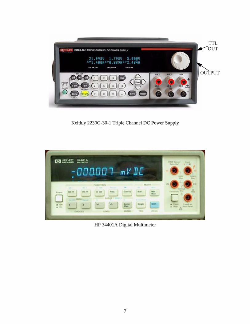
Keithly 2230G-30-1 Triple Channel DC Power Supply
HP 34401A Digital Multimeter
TTL
OUTPUT
OUT
8
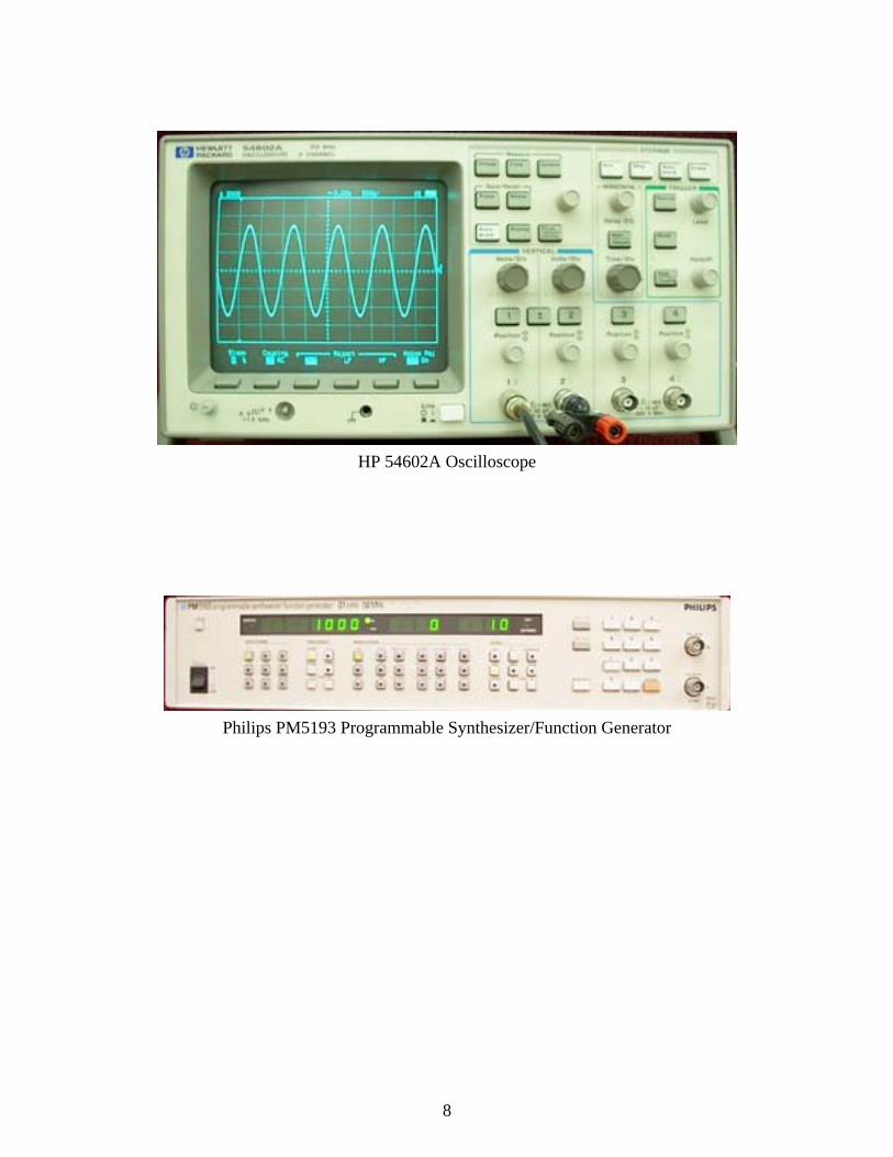
HP 54602A Oscilloscope
Philips PM5193 Programmable Synthesizer/Function Generator
Lab 1
9
Laboratory 1
Introduction - Resistor Codes, Breadboard, and Basic Measurements
Required Components:• 3 1k resistors
1.1 Introduction and Objectives
Welcome to the world of mechatronics. Your experiences in this laboratory will provide asolid foundation in instrumentation and modern electronics. The purpose of the first laboratoryexercise is to familiarize you with the laboratory facilities and procedures, and with basicmeasurement techniques. The specific objectives are:
• Observe demonstrations of the instruments that you will use throughout the semester.These instruments include the oscilloscope, digital multimeter, power supply, andfunction generator.
• Learn how to construct basic electrical circuits using a breadboard.
• Learn how to properly take voltage and current measurements in circuits.
• Learn the resistor color code scheme necessary to read resistor values and tolerances.
• Learn about the types of capacitors and how to read their values.
1.2 Electrical Safety
Electrical voltages and currents can be dangerous if they occur at values that interfere withphysiological functions. All of the laboratory exercises described in this manual are designed touse ac and dc voltages whose values are less than 15 V, values that will not cause perceptible shockvia the skin. If working with voltages higher than these, especially line voltages (110 Vrms or 220Vrms), one must be extremely careful to avoid shock or potentially lethal situations. We cautionthe user of household voltages and currents to carefully read the electrical safety precautionsoutlined in the textbook (see Section 2.10.1).
1.3 Resistor Color Codes
The most common electrical component found in almost every electrical circuit is aresistor. The type we will use in the Lab is the 1/4 watt axial-lead resistor. A resistor's value andtolerance are usually coded with four colored bands (a, b, c, tol) as illustrated in Figure 1.1. Thecolors used for bands are listed with their respective values in Table 1.1. A resistor's value andtolerance are expressed as

10
(1.1)
where the a band represents the tens digit, the b band represents the ones digit, the c band representsthe power of 10, and the tol band represents the tolerance or uncertainty as a percentage of thecoded resistance value. The set of standard values for the first two digits are: 10, 11, 12, 13, 14, 15,16, 18, 20, 22, 24, 27, 30, 33, 36, 39, 43, 47, 51, 56, 62, 68, 75, 82, and 91.
Figure 1.1 Wire lead resistor color bands
Table 1.1 Resistor color band codes
1.4 Reading Capacitor values
Most students learn to read resistor values quite easily. However, they often have moretrouble picking out a specific capacitor. That's not their fault. They have trouble, as you will agreewhen you have finished reading this, because the capacitor manufacturers don't want them to beable to read cap values. ("Cap" is shorthand for "capacitor," as you probably know.) The capmarkings have been designed by an intergalactic committee to be nearly unintelligible. With a fewhints, however, you can learn to read cap markings, despite the manufacturers' efforts to preventthis. Some hints for various size capacitors follow.
a, b, and c Bands tol Band
Color Value Color Value
Black 0 Gold ±5%
Brown 1 Silver ±10%
Red 2 Nothing ±20%
Orange 3
Yellow 4
Green 5
Blue 6
Violet 7
Gray 8
White 9
R ab 10c tol %=
a b c tol
Lab 1
11
Big Capacitors
Big Caps are usually the electrolytic type. These are easy to read, because there is room toprint the value on the cap, including units. You need only have the common sense to assume that,for example, +500MF means 500 micro farads, with the plus indicating the positive end of thecapacitor. Be careful to not take the capital M seriously. (Remember the SI system of units?)
All of these big caps are polarized. That means the capacitor's innards are not symmetrical,and that you may destroy the cap if you apply the wrong polarity to the terminals: the terminalmarked + must be at least as positive as the other terminal. (Sometimes, violating this rule willform gas that makes the cap blow up; more often, the cap will short internally.
Smaller Capacitors
As the caps get smaller, the difficulty in reading their markings gets steadily worse.Tantalum caps are silver colored cylinders. They are polarized: a + mark and a metal nipple markthe positive end. Their markings may say something like +4R7. That also means pretty muchwhat it says, if you know that the "R" marks the decimal place: it's a 4.7 F cap.
The same cap could also be marked +475K. Here you encounter your first challenge, butalso the first appearance of an orderly scheme for labeling caps, a scheme that would be helpful ifit were used more widely. The challenge is to resist the plausible assumption that "K" means"kilo." It does not; it is not a unit marking, but a tolerance notation (it means ± 10%). (Wasn't thatnasty of the labelers to choose "K?" Guess what's another favorite letter for tolerance. That's right:M. Pretty mean!) The orderly labeling here mimics the resistor codes: 475 means 47 times ten tothe fifth power. But what are the Units? 105 what? 105 of something small. You will meet thisdilemma repeatedly, and you must resolve it by relying on the following intuitive observations:
1. The only units commonly used in this country are
microfarads: 10-6 Farad
picofarads: 10-12 Farad
(you should, therefore, avoid using "mF" and "nF" yourself.)
A Farad is a humongous unit. The biggest cap you will use in this course is 500 F.It is physically large (we do keep 1F caps around, but only for our freak show). Thus,if you find a small cap labeled "470," you know it is 470pF.
2. A picofarad is a tiny unit. You will not see a cap as small as 1 pF in this course. So, ifyou find a cap appearing to claim that it is a fraction of some unprinted unit say, ".01" the unit is F: ".01" means 0.01 F.
3. A picofarad is not just a bit smaller than a microfarad. A pF is not 10-9F (10-3 F);instead, it is 10-12 F: a million times smaller than a microfarad!
So, we conclude, a cap labeled "475" must be 4.7 x 10⁶ (47 x 105) picofarads. That, youwill recognize, is a roundabout way to say 4.7 x 10⁻⁶ F or 4.7 F.

12
We knew that this was the answer, before we started this last decoding effort. This way oflabeling is quite roundabout, but at least it is unambiguous. It would be nice to see it used morewidely. You will see another example of this exponential labeling in the case of the CK05 ceramiccaps, below.
Mylar caps are yellow cylinders, that are rather clearly marked. ".01M" is just 0.01 F, ofcourse; and ".1 MFD" is not a tenth of a megafarad. You can orient them at random in your circuits.Because they are fabricated as long coils of metal foil (separated by a thin dielectric - the "mylar"that gives them their name), mylar caps must betray their function at very high frequencies: that is,they begin to behave as inductors instead, blocking the very high frequencies they ought to pass.Ceramics (below) do better in this respect, although they are very poor in other characteristics.
Ceramic caps are little orange pancakes. Because of this shape (in contrast to the coilformat hidden within the tubular shape of mylars) they act like capacitors even at high frequencies.The trick, in reading these, is to reject the markings that should not be interpreted as units. Forexample, a ceramic disk cap labeled by "Z5U .02M 1kV" is a 0.02 F cap with a maximum voltagerating of 1kV. The M is a tolerance marking, in this case (see below), ±20%.
CK05 caps are little boxes, with their leads 0.2" apart so they can be easily inserted inprotoboards (AKA perf boards or vector boards) or PC boards. Therefore, they are common anduseful. An example marking is 101K. This is the neat resistor-like marking. This one is 100 pF(10 x 101 pF).
Tolerance Codes
Finally, just to be thorough, and because this information is hard to come by, let's list allthe tolerance codes. These apply to both capacitors and resistors; the tight tolerances are relevantonly to resistors; the strangely asymmetric tolerance is used only for capacitors.
Tolerance Code Meaning
Z +80%,-20% M ±20%K ± 10%J ±5%G ±2%F ±1%D ±0.5%C ±0.25%B ± 0.1%A ± 0.005Z ± 0.025 (precision resistors; context will show the asymmetric cap
cap tolerance "Z" makes no sense here)N ±0.02%
Lab 1
13
1.5 The Breadboard
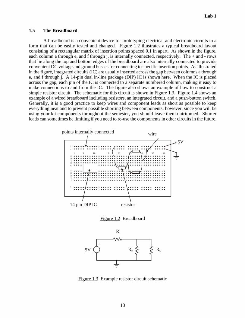
A breadboard is a convenient device for prototyping electrical and electronic circuits in aform that can be easily tested and changed. Figure 1.2 illustrates a typical breadboard layoutconsisting of a rectangular matrix of insertion points spaced 0.1 in apart. As shown in the figure,each column a through e, and f through j, is internally connected, respectively. The + and - rowsthat lie along the top and bottom edges of the breadboard are also internally connected to provideconvenient DC voltage and ground busses for connecting to specific insertion points. As illustratedin the figure, integrated circuits (IC) are usually inserted across the gap between columns a throughe, and f through j. A 14-pin dual in-line package (DIP) IC is shown here. When the IC is placedacross the gap, each pin of the IC is connected to a separate numbered column, making it easy tomake connections to and from the IC. The figure also shows an example of how to construct asimple resistor circuit. The schematic for this circuit is shown in Figure 1.3. Figure 1.4 shows anexample of a wired breadboard including resistors, an integrated circuit, and a push-button switch.Generally, it is a good practice to keep wires and component leads as short as possible to keepeverything neat and to prevent possible shorting between components; however, since you will beusing your kit components throughout the semester, you should leave them untrimmed. Shorterleads can sometimes be limiting if you need to re-use the components in other circuits in the future.
Figure 1.2 Breadboard
Figure 1.3 Example resistor circuit schematic
+
abcde
fghij
1 5 10 15 20 25 30 35 40
+
points internally connected
5V
14 pin DIP IC
wire
resistor
+
5V
R1
R3R2
14
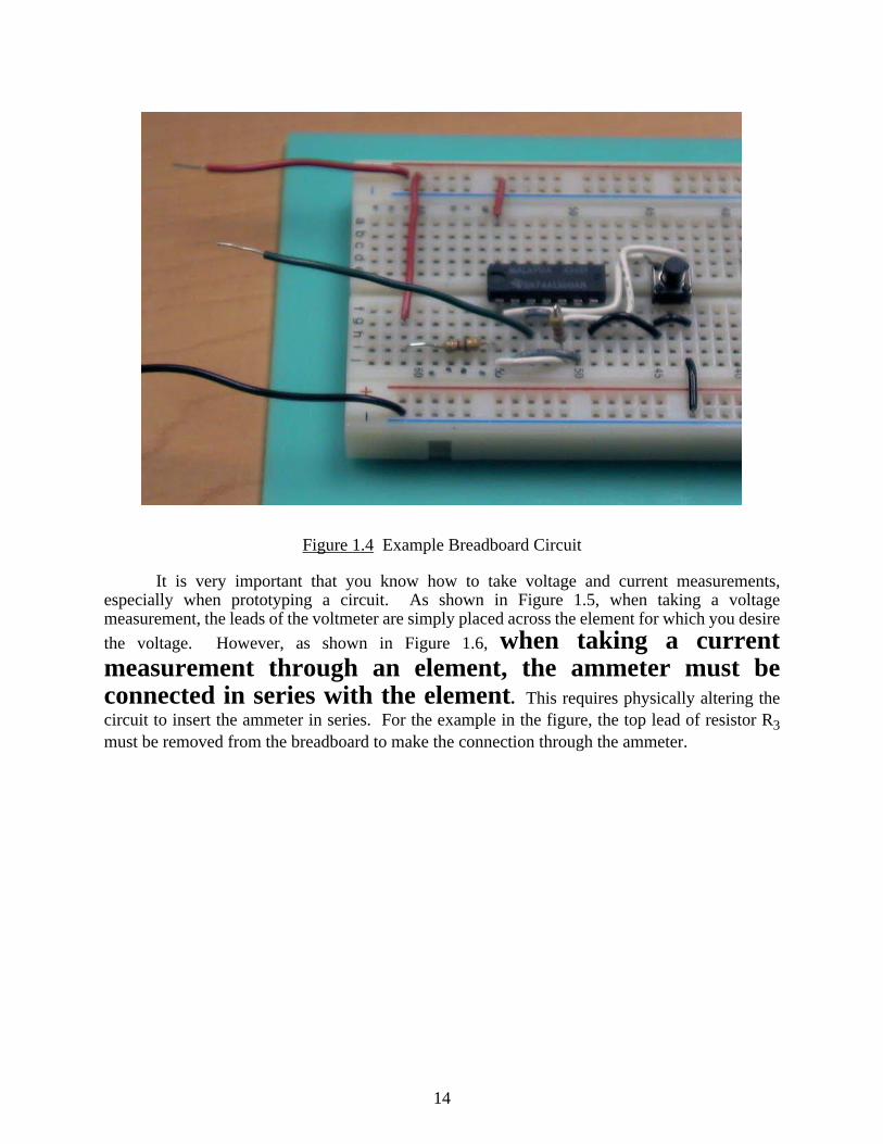
Figure 1.4 Example Breadboard Circuit
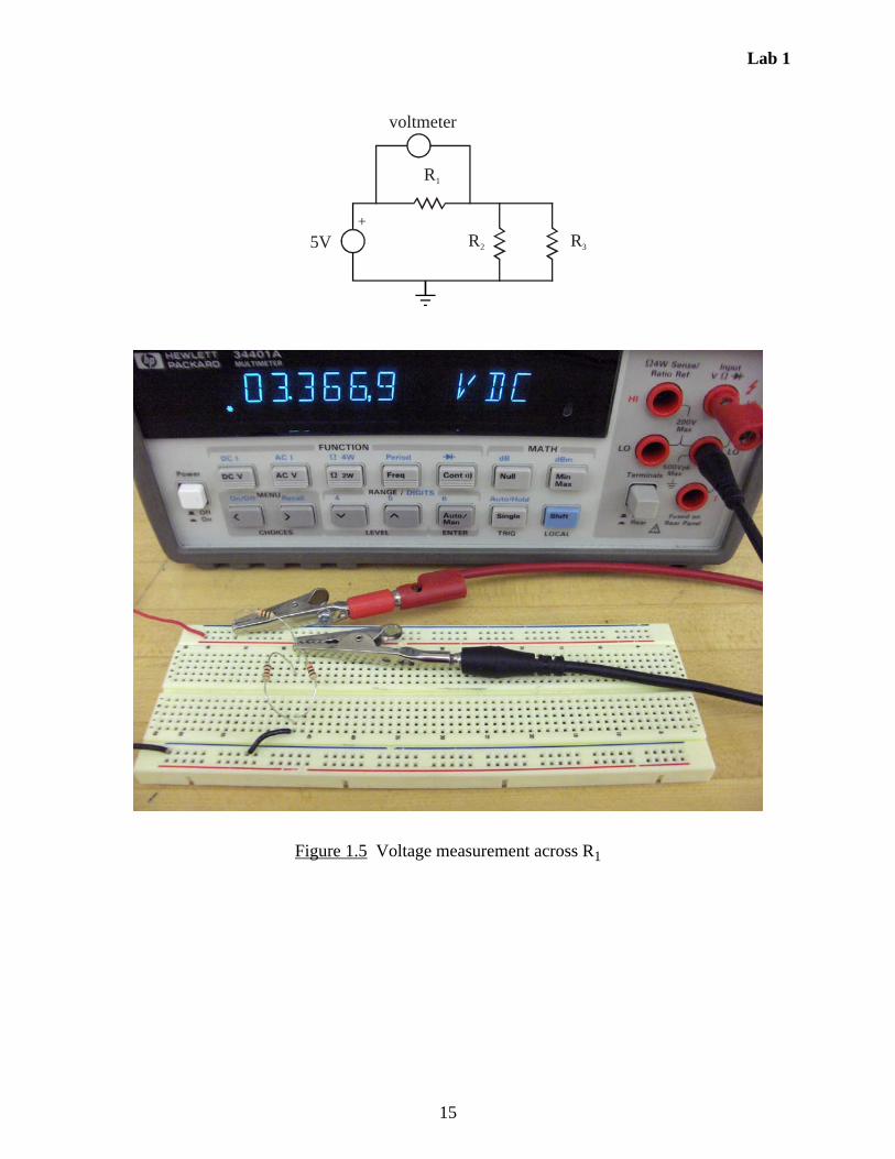
It is very important that you know how to take voltage and current measurements,especially when prototyping a circuit. As shown in Figure 1.5, when taking a voltagemeasurement, the leads of the voltmeter are simply placed across the element for which you desire
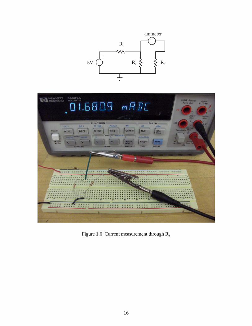
the voltage. However, as shown in Figure 1.6, when taking a currentmeasurement through an element, the ammeter must beconnected in series with the element. This requires physically altering thecircuit to insert the ammeter in series. For the example in the figure, the top lead of resistor R3must be removed from the breadboard to make the connection through the ammeter.
Lab 1
15
Figure 1.5 Voltage measurement across R1
+
5V
R1
R3R2
voltmeter
16
Figure 1.6 Current measurement through R3
+
5V
R1
R3R2
ammeter

Lab 1
17
1.6 Laboratory Procedure / Summary Sheet
Group: ____ Names: _________________________ _____________________________
_________________________ _____________________________
(1) For a 1k resistor, what are the color band colors and associated band values?
What is the expected nominal resistance and tolerance (in Ohms)?
R = ________________________ _____________ (not %)
Rmin = ____________________ Rmax = ____________________
(2) Select three 1k resistors, and measure the resistance of each using the digitalmultimeter and compare the values with the specified value.
band color value
a
b
c
tol
Resistor Measured Value () % Error
R1
R2
R3
18
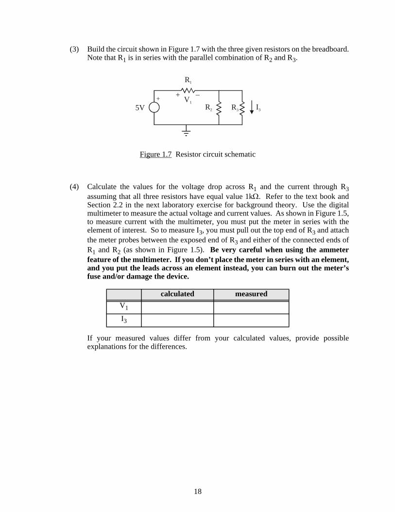
(3) Build the circuit shown in Figure 1.7 with the three given resistors on the breadboard.Note that R1 is in series with the parallel combination of R2 and R3.
Figure 1.7 Resistor circuit schematic
(4) Calculate the values for the voltage drop across R1 and the current through R3assuming that all three resistors have equal value 1k. Refer to the text book andSection 2.2 in the next laboratory exercise for background theory. Use the digitalmultimeter to measure the actual voltage and current values. As shown in Figure 1.5,to measure current with the multimeter, you must put the meter in series with theelement of interest. So to measure I3, you must pull out the top end of R3 and attachthe meter probes between the exposed end of R3 and either of the connected ends ofR1 and R2 (as shown in Figure 1.5). Be very careful when using the ammeterfeature of the multimeter. If you don’t place the meter in series with an element,and you put the leads across an element instead, you can burn out the meter’sfuse and/or damage the device.
If your measured values differ from your calculated values, provide possibleexplanations for the differences.
calculated measured
V1
I3
+
5V
R1
R3R2
+ V1
I3

Lab 2
19
Laboratory 2
Instrument Familiarization and Basic Electrical Relations
Required Components:• 2 1k resistors• 2 1M resistors• 1 2k resistor
2.1 Objectives
This exercise is designed to acquaint you with the following laboratory instruments whichwill be used throughout the semester:
• The Oscilloscope
• The Digital Multimeter (DMM)
• The Triple Output DC power Supply
• The AC Function Generator
During the course of this laboratory exercise you should also obtain a thorough workingknowledge of the following electrical relations:
• Series and Parallel Equivalent Resistance
• Kirchoff's Current Law (KCL)
• Kirchoff's Voltage Law (KVL)
• Ohm's Law
• The Voltage Divider Rule
• The Current Divider Rule
The experiments to be performed during this laboratory are also designed to introduce youto two very important instrument characteristics:
• The output impedance of a real source
• The input impedance of a real instrument
Lab 2
20
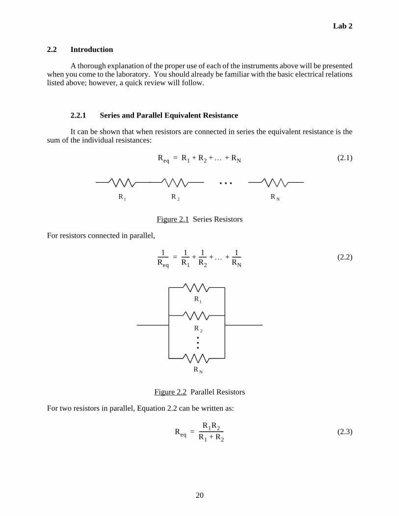
2.2 Introduction
A thorough explanation of the proper use of each of the instruments above will be presentedwhen you come to the laboratory. You should already be familiar with the basic electrical relationslisted above; however, a quick review will follow.
2.2.1 Series and Parallel Equivalent Resistance
It can be shown that when resistors are connected in series the equivalent resistance is thesum of the individual resistances:
(2.1)
Figure 2.1 Series Resistors
For resistors connected in parallel,
(2.2)
Figure 2.2 Parallel Resistors
For two resistors in parallel, Equation 2.2 can be written as:
(2.3)
Req R1 R2 RN+ + +=
R1 R 2 R N
…
1Req-------- 1
R1------ 1
R2------ 1
RN-------+ + +=
R1
R 2
R N
…
Req
R1R2
R1 R2+-------------------=
Lab 2
21
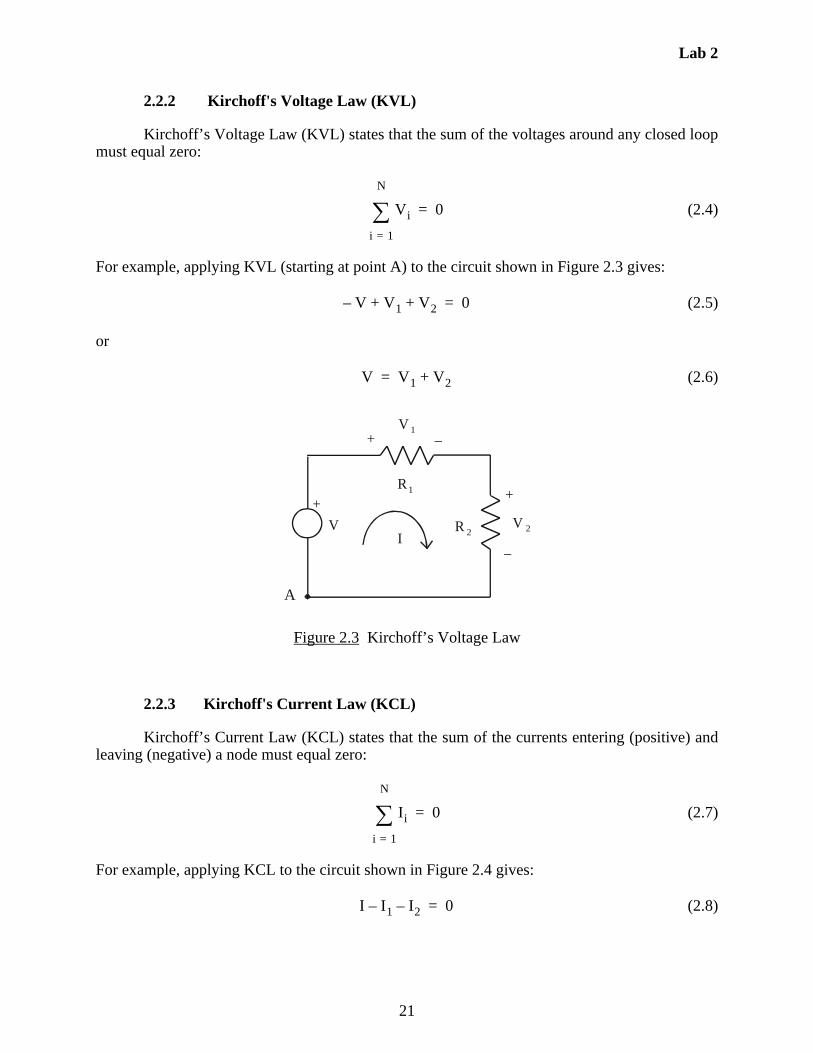
2.2.2 Kirchoff's Voltage Law (KVL)
Kirchoff’s Voltage Law (KVL) states that the sum of the voltages around any closed loopmust equal zero:
(2.4)
For example, applying KVL (starting at point A) to the circuit shown in Figure 2.3 gives:
(2.5)
or
(2.6)
Figure 2.3 Kirchoff’s Voltage Law
2.2.3 Kirchoff's Current Law (KCL)
Kirchoff’s Current Law (KCL) states that the sum of the currents entering (positive) andleaving (negative) a node must equal zero:
(2.7)
For example, applying KCL to the circuit shown in Figure 2.4 gives:
(2.8)
Vi
i 1=
N
0=
V– V1 V2+ + 0=
V V1 V2+=
R1
R 2
+
VI
V 2
V 1+ –
+
–
A
Ii
i 1=
N
0=
I I1– I2– 0=
Lab 2
22
or
(2.9)
Figure 2.4 Kirchoff’s Current Law
2.2.4 Ohm's Law
Ohm’s Law states that the voltage across an element is equal to the resistance of the elementtimes the current through it:
(2.10)
Figure 2.5 Ohm’s Law
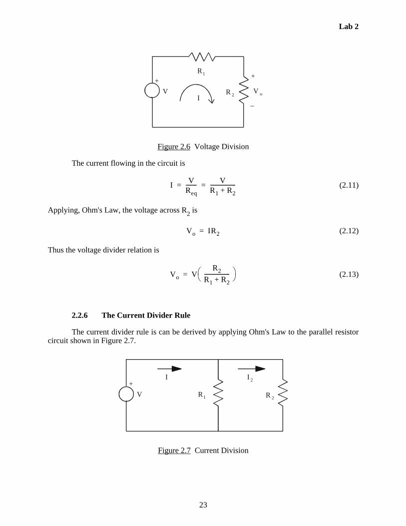
2.2.5 The Voltage Divider Rule
The voltage divider rule is an extension of Ohm's Law and can be applied to a series resistorcircuit shown in Figure 2.6.
I I1 I2+=
I1
I 2
I
V IR=
+ –V
I
Lab 2
23
Figure 2.6 Voltage Division
The current flowing in the circuit is
(2.11)
Applying, Ohm's Law, the voltage across R2 is
(2.12)
Thus the voltage divider relation is
(2.13)
2.2.6 The Current Divider Rule
The current divider rule is can be derived by applying Ohm's Law to the parallel resistorcircuit shown in Figure 2.7.
Figure 2.7 Current Division
R1
R 2
+
VI
+
–
V o
IV
Req-------- V
R1 R2+-------------------= =
Vo IR2=
Vo V R2
R1 R2+-------------------
=
R1 R 2
+
V
I I 2
Lab 2
24
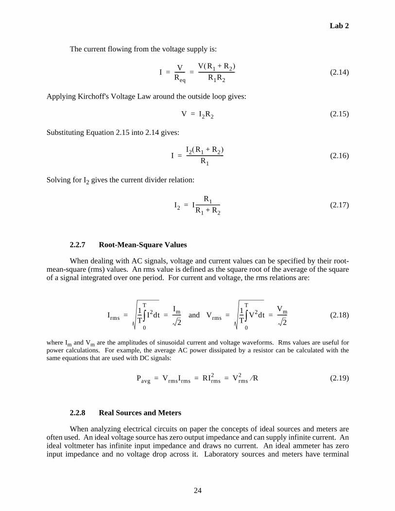
The current flowing from the voltage supply is:
(2.14)
Applying Kirchoff's Voltage Law around the outside loop gives:
(2.15)
Substituting Equation 2.15 into 2.14 gives:
(2.16)
Solving for I2 gives the current divider relation:
(2.17)
2.2.7 Root-Mean-Square Values
When dealing with AC signals, voltage and current values can be specified by their root-mean-square (rms) values. An rms value is defined as the square root of the average of the squareof a signal integrated over one period. For current and voltage, the rms relations are:
and (2.18)
where Im and Vm are the amplitudes of sinusoidal current and voltage waveforms. Rms values are useful forpower calculations. For example, the average AC power dissipated by a resistor can be calculated with thesame equations that are used with DC signals:
(2.19)
2.2.8 Real Sources and Meters
When analyzing electrical circuits on paper the concepts of ideal sources and meters areoften used. An ideal voltage source has zero output impedance and can supply infinite current. Anideal voltmeter has infinite input impedance and draws no current. An ideal ammeter has zeroinput impedance and no voltage drop across it. Laboratory sources and meters have terminal
IV
Req--------
V R1 R2+ R1R2
----------------------------= =
V I2R2=
II2 R1 R2+
R1-----------------------------=
I2 IR1
R1 R2+-------------------=
Irms1T--- I2dt
0
T
Im
2-------= = Vrms
1T--- V2dt
0
T
Vm
2--------= =
Pavg VrmsIrms RIrms2 Vrms
2 R= = =
Lab 2
25
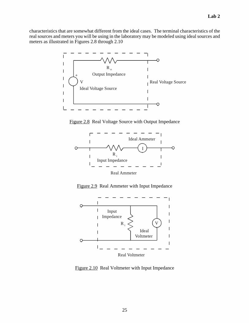
characteristics that are somewhat different from the ideal cases. The terminal characteristics of thereal sources and meters you will be using in the laboratory may be modeled using ideal sources andmeters as illustrated in Figures 2.8 through 2.10
Figure 2.8 Real Voltage Source with Output Impedance
Figure 2.9 Real Ammeter with Input Impedance
Figure 2.10 Real Voltmeter with Input Impedance
+
V
R o
Output Impedance
Ideal Voltage Source
Real Voltage Source
Input Impedance
Ideal Ammeter
Real Ammeter
IR i
Input Impedance
Ideal Voltmeter
Real Voltmeter
R i V
Lab 2
26
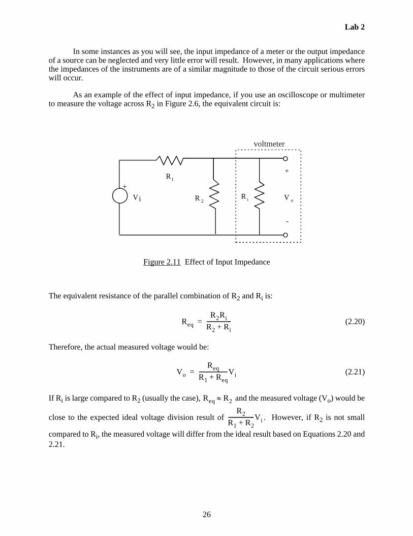
In some instances as you will see, the input impedance of a meter or the output impedanceof a source can be neglected and very little error will result. However, in many applications wherethe impedances of the instruments are of a similar magnitude to those of the circuit serious errorswill occur.
As an example of the effect of input impedance, if you use an oscilloscope or multimeterto measure the voltage across R2 in Figure 2.6, the equivalent circuit is:
Figure 2.11 Effect of Input Impedance
The equivalent resistance of the parallel combination of R2 and Ri is:
(2.20)
Therefore, the actual measured voltage would be:
(2.21)
If Ri is large compared to R2 (usually the case), and the measured voltage (Vo) would be
close to the expected ideal voltage division result of . However, if R2 is not small
compared to Ri, the measured voltage will differ from the ideal result based on Equations 2.20 and2.21.
R1
R 2
+
Vi V o
+
-
R i
voltmeter
Req
R2Ri
R2 Ri+------------------=
Vo
Req
R1 Req+---------------------Vi=
Req R2
R2
R1 R2+-------------------Vi

Lab 2
27
If you know values for Vi, R1, and R2 in Figure 2.11, and if you measure Vo, you candetermine the input impedance (Ri) of the measuring device using the following analysis. Equation2.21 can be solved for Req giving:
(2.22)
Knowing Req, we can determine the input impedance by solving for Ri in Equation 2.20:
(2.23)
2.3 Circuit Troubleshooting Advice
When your circuits don’t work properly in this andfuture Labs (and in your Project), always go through thefollowing set of checks to help diagnose and fix any problems:
(1) Verify that your breadboard circuit is constructed properly based on the circuitschematic or wiring diagram by checking each connection, making sure thebreadboard is being used properly per Figure 1.2 in Lab 1.
(2) Use the continuity-check feature of the multimeter to verify that wiring andconnections are good between all source and terminus pins.
(3) Make sure power and ground are available where needed on the breadboard, andinclude jumper wires between the top and bottom power and ground rows ifnecessary.
(4) Make sure you have common grounds among your circuit and all instrumentationbeing used (power supply, function generator, multimeter, oscilloscope).
(5) Check the power supply voltage with the multimeter to make sure it is at the correctlevel.
(6) Take voltage measurements in different parts of the circuit to make sure values matchwhat is expected.
And for additional troubleshooting advice, especially formore-complicated circuits and the Project, see Section 7.4 inLab 7 and Section 15.5 in Lab 15.
Req
Vo
Vi Vo–------------------ R1=
Ri
ReqR2
R2 Req– --------------------------=

Lab 2
28
Lab 2
29
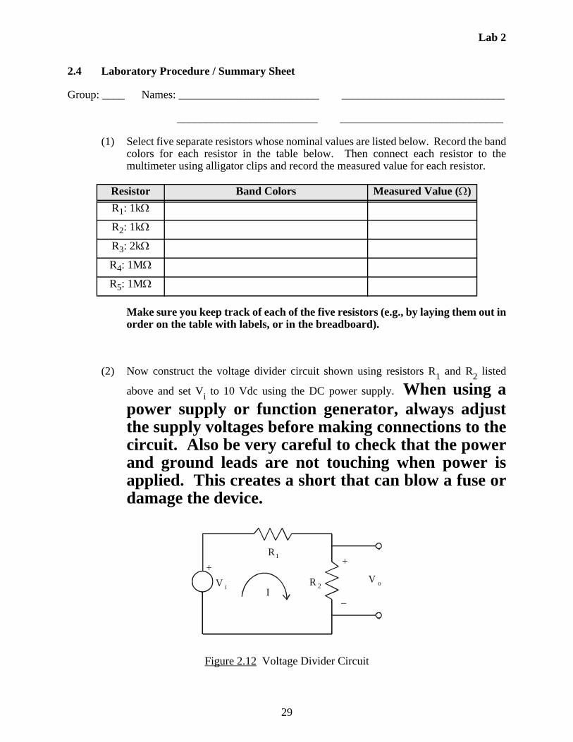
2.4 Laboratory Procedure / Summary Sheet
Group: ____ Names: _________________________ _____________________________
_________________________ _____________________________
(1) Select five separate resistors whose nominal values are listed below. Record the bandcolors for each resistor in the table below. Then connect each resistor to themultimeter using alligator clips and record the measured value for each resistor.
Make sure you keep track of each of the five resistors (e.g., by laying them out inorder on the table with labels, or in the breadboard).
(2) Now construct the voltage divider circuit shown using resistors R1 and R2 listed
above and set Vi to 10 Vdc using the DC power supply. When using apower supply or function generator, always adjustthe supply voltages before making connections to thecircuit. Also be very careful to check that the powerand ground leads are not touching when power isapplied. This creates a short that can blow a fuse ordamage the device.
Figure 2.12 Voltage Divider Circuit
Resistor Band Colors Measured Value ()
R1: 1k
R2: 1k
R3: 2k
R4: 1M
R5: 1M
R1
R 2
+
I
+
–
V oV i
Lab 2
30
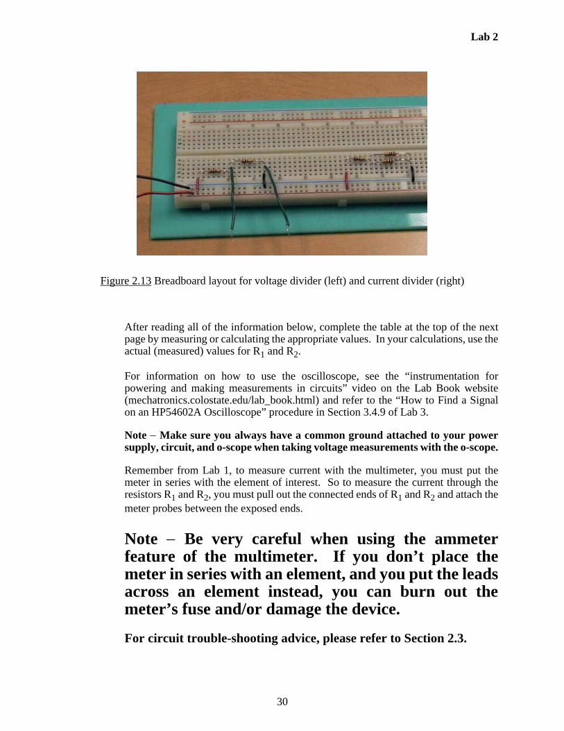
Figure 2.13 Breadboard layout for voltage divider (left) and current divider (right)
After reading all of the information below, complete the table at the top of the nextpage by measuring or calculating the appropriate values. In your calculations, use theactual (measured) values for R1 and R2.
For information on how to use the oscilloscope, see the “instrumentation forpowering and making measurements in circuits” video on the Lab Book website(mechatronics.colostate.edu/lab_book.html) and refer to the “How to Find a Signalon an HP54602A Oscilloscope” procedure in Section 3.4.9 of Lab 3.
Note Make sure you always have a common ground attached to your powersupply, circuit, and o-scope when taking voltage measurements with the o-scope.
Remember from Lab 1, to measure current with the multimeter, you must put themeter in series with the element of interest. So to measure the current through theresistors R1 and R2, you must pull out the connected ends of R1 and R2 and attach themeter probes between the exposed ends.
Note Be very careful when using the ammeterfeature of the multimeter. If you don’t place themeter in series with an element, and you put the leadsacross an element instead, you can burn out themeter’s fuse and/or damage the device.
For circuit trouble-shooting advice, please refer to Section 2.3.
Lab 2
31
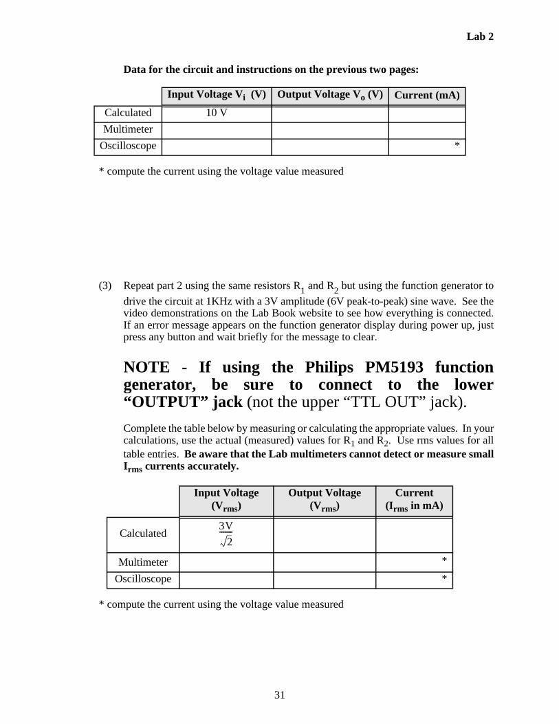
Data for the circuit and instructions on the previous two pages:
* compute the current using the voltage value measured
(3) Repeat part 2 using the same resistors R1 and R2 but using the function generator to
drive the circuit at 1KHz with a 3V amplitude (6V peak-to-peak) sine wave. See thevideo demonstrations on the Lab Book website to see how everything is connected.If an error message appears on the function generator display during power up, justpress any button and wait briefly for the message to clear.
NOTE - If using the Philips PM5193 functiongenerator, be sure to connect to the lower“OUTPUT” jack (not the upper “TTL OUT” jack).
Complete the table below by measuring or calculating the appropriate values. In yourcalculations, use the actual (measured) values for R1 and R2. Use rms values for alltable entries. Be aware that the Lab multimeters cannot detect or measure smallIrms currents accurately.
* compute the current using the voltage value measured
Input Voltage Vi (V) Output Voltage Vo (V) Current (mA)
Calculated 10 V
Multimeter
Oscilloscope *
Input Voltage (Vrms)
Output Voltage (Vrms)
Current(Irms in mA)
Calculated
Multimeter *
Oscilloscope *
3V
2-------

Lab 2
32
(4) Repeat part 2 (Vi = 10 Vdc) using R4 and R5 in place of R1 and R2. In this case, the
impedances of the instruments are close in value to the load resistances and thereforeaffect the measured values. Sketch the equivalent circuit for the instruments (voltagesupply, and voltmeter or oscilloscope) and the attached circuit. Use this schematic toexplain differences between actual (measured) and theoretical values.
Complete the table below by measuring or calculating the appropriate values. In yourcalculations, use the actual (measured) values for R4 and R5.
*: compute the current using the voltage value measured since current cannot bemeasured directly on an oscilloscope and since the currents are too small tomeasure on the NI ELVIS.
Input Voltage (V) Output Voltage (V) Current (mA)*
Calculated
Multimeter
Oscilloscope
Lab 2
33
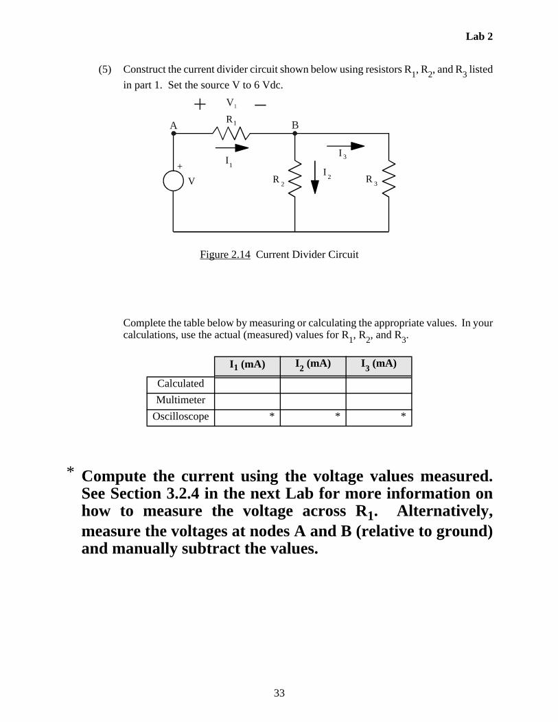
(5) Construct the current divider circuit shown below using resistors R1, R2, and R3 listed
in part 1. Set the source V to 6 Vdc.
Figure 2.14 Current Divider Circuit
Complete the table below by measuring or calculating the appropriate values. In yourcalculations, use the actual (measured) values for R1, R2, and R3.
* Compute the current using the voltage values measured.See Section 3.2.4 in the next Lab for more information onhow to measure the voltage across R1. Alternatively,measure the voltages at nodes A and B (relative to ground)and manually subtract the values.
I1 (mA) I2 (mA) I3 (mA)
Calculated
Multimeter
Oscilloscope * * *
R1
R2
+
VI
2 R 3
I1
I 3
V1
A B
Lab 2
34
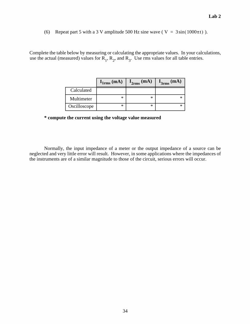
(6) Repeat part 5 with a 3 V amplitude 500 Hz sine wave ( ).
Complete the table below by measuring or calculating the appropriate values. In your calculations,use the actual (measured) values for R1, R2, and R3. Use rms values for all table entries.
* compute the current using the voltage value measured
Normally, the input impedance of a meter or the output impedance of a source can beneglected and very little error will result. However, in some applications where the impedances ofthe instruments are of a similar magnitude to those of the circuit, serious errors will occur.
I1rms (mA) I2rms (mA) I3rms (mA)
Calculated
Multimeter * * *
Oscilloscope * * *
V 3 1000t sin=

Lab 2
35
LAB 2 QUESTIONS
Group: ____ Names: _________________________ _____________________________
_________________________ _____________________________
(1) Describe how you read resistor values and tolerances.
(2) Derive formulas, using the voltage divider and current divider rules, for the followingvoltage and current in Figure 2.14, using V, R1, R2, and R3 only.
V1 = _________________________ I3 = __________________________
(3) From the data collected in Part 4, calculate the input impedance of the oscilloscope and thevoltmeter.
Zin (scope) = _________________________
Zin (DMM) = _________________________
Hint: Use Equations 2.22 and 2.23. Also, if using the attenuator probe, be sure to accountfor the probe’s impedance (see Section 3.3 in Lab 3).
(4) The AC wall outlet provides 110 Vrms at 60Hz. Sketch and label one period of this
waveform.

Lab 2
36
(5) Using a function generator and three 1 k resistors design a circuit that will supply both a6V p-p output and a 2V p-p output. Show your work below.

Lab 3
37
Laboratory 3
The Oscilloscope
Required Components:• 1 10 resistor• 2 100 resistors• 2 1k resistors• 1 2k resistor• 2 4.7M resistors• 1 0.022F capacitor• 1 0.1F capacitor• 1 1.0F capacitor
3.1 Objectives
In the previous laboratory exercise you learned about the basic operation of theoscilloscope. This laboratory exercise is designed to give you a more in-depth understanding ofthe proper use of the oscilloscope and its range of applications.
The oscilloscope is probably one of the most widely used electrical instruments and is oneof the most misunderstood. During the course of this laboratory exercise you will become familiarwith the proper methods of connecting inputs, grounding, coupling, and triggering theoscilloscope. Also during the course of this experiment you will learn the proper use of theoscilloscope attenuator probe.
3.2 Introduction
3.2.1 AC and DC Signals
An AC signal varies with time, and its deterministic expression contains time as theindependent variable. For example,
(3.1)
(3.2)
A DC signal on the other hand does not vary with time, hence t does not appear in its expression:
(3.3)
(3.4)
F1 t 2.0 5tsin=
F2 t 3.1 5tcos 5.1e3.0t–
+=
F3 t 1.0=
F4 t 5.63=
Lab 3
38
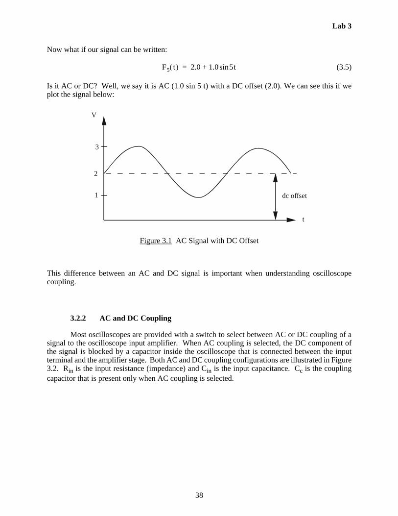
Now what if our signal can be written:
(3.5)
Is it AC or DC? Well, we say it is AC (1.0 sin 5 t) with a DC offset (2.0). We can see this if weplot the signal below:
Figure 3.1 AC Signal with DC Offset
This difference between an AC and DC signal is important when understanding oscilloscopecoupling.
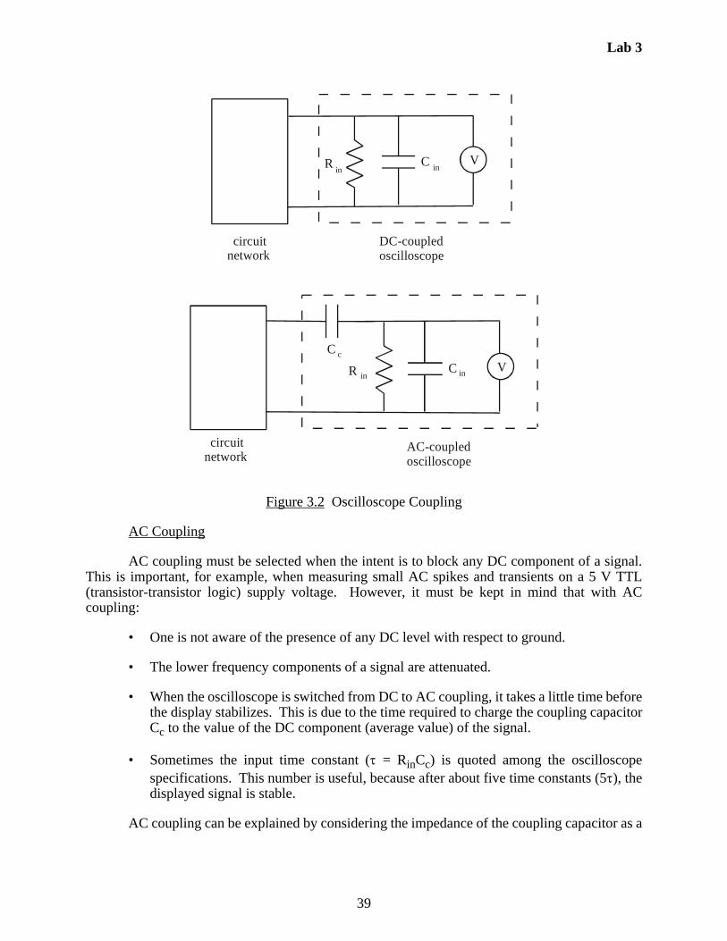
3.2.2 AC and DC Coupling
Most oscilloscopes are provided with a switch to select between AC or DC coupling of asignal to the oscilloscope input amplifier. When AC coupling is selected, the DC component ofthe signal is blocked by a capacitor inside the oscilloscope that is connected between the inputterminal and the amplifier stage. Both AC and DC coupling configurations are illustrated in Figure3.2. Rin is the input resistance (impedance) and Cin is the input capacitance. Cc is the couplingcapacitor that is present only when AC coupling is selected.
F5 t 2.0 1.0 5tsin+=
V
dc offset1
2
3
t
Lab 3
39
Figure 3.2 Oscilloscope Coupling
AC Coupling
AC coupling must be selected when the intent is to block any DC component of a signal.This is important, for example, when measuring small AC spikes and transients on a 5 V TTL(transistor-transistor logic) supply voltage. However, it must be kept in mind that with ACcoupling:
• One is not aware of the presence of any DC level with respect to ground.
• The lower frequency components of a signal are attenuated.
• When the oscilloscope is switched from DC to AC coupling, it takes a little time beforethe display stabilizes. This is due to the time required to charge the coupling capacitorCc to the value of the DC component (average value) of the signal.
• Sometimes the input time constant ( = RinCc) is quoted among the oscilloscopespecifications. This number is useful, because after about five time constants (5), thedisplayed signal is stable.
AC coupling can be explained by considering the impedance of the coupling capacitor as a
Rin
C in
circuit network
DC-coupled oscilloscope
V
R inC in
circuit network
AC-coupled oscilloscope
VC c
Lab 3
40
function of frequency:
(3.6)
where j represents the imaginary number . With a DC voltage = 0) the impedance of thecapacitor is infinite, and all of the DC voltage at the input terminals of the oscilloscope will appearacross the capacitor. Thus, AC-coupling the oscilloscope will eliminate any DC offset present inthe voltage appearing across the input terminals of the oscilloscope. For AC signals, theimpedance is less than infinite, resulting in attenuation of the input signal dependent upon thefrequency. As the input frequency increases the attenuation decreases to zero. The coupling modeis selected using the input selectors on the front panel of the oscilloscope. Generally, if the signaltype is unknown, DC coupling is the first choice for observing the signal.
3.2.3 Triggering the Oscilloscope
Triggering refers to an event at the input terminals of the oscilloscope that causes theelectron beam to sweep across the screen and display the terminal voltage. The oscilloscope maybe level triggered either in the AC or DC mode, and the level of the magnitude is adjustable usingthe trigger level control. The slope (+ or –) of the terminal voltage also affects when the beam istriggered. This slope is selected either positive or negative.
Another triggering option available is that of line triggering. Line triggering uses the ACpower input to synchronize the sweep. Thus, any terminal voltage synchronized with the linefrequency of 60Hz or multiples of 60Hz can be triggered in this mode. This is useful to detect if60 Hz noise from various line related sources is superimposed on the signal.
3.2.4 Grounding Source and Scope
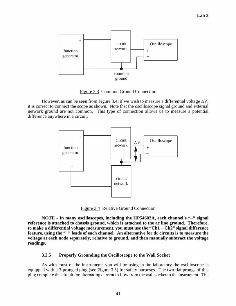
Normally, all measurement instruments, power sources, and signal sources in a circuit mustbe referenced to a common ground as shown in Figure 3.3.
Z1
jC----------=
1–
Lab 3
41
Figure 3.3 Common Ground Connection
However, as can be seen from Figure 3.4, if we wish to measure a differential voltage V,it is correct to connect the scope as shown. Note that the oscilloscope signal ground and externalnetwork ground are not common. This type of connection allows us to measure a potentialdifference anywhere in a circuit.
Figure 3.4 Relative Ground Connection
NOTE - In many oscilloscopes, including the HP54602A, each channel’s “” signalreference is attached to chassis ground, which is attached to the ac line ground. Therefore,to make a differential voltage measurement, you must use the “Ch1 Ch2” signal differencefeature, using the “+” leads of each channel. An alternative for dc circuits is to measure thevoltage at each node separately, relative to ground, and then manually subtract the voltagereadings.
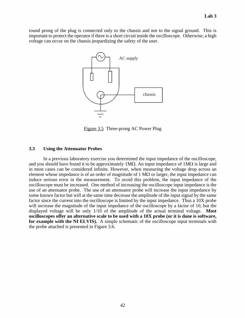
3.2.5 Properly Grounding the Oscilloscope to the Wall Socket
As with most of the instruments you will be using in the laboratory the oscilloscope isequipped with a 3-pronged plug (see Figure 3.5) for safety purposes. The two flat prongs of thisplug complete the circuit for alternating current to flow from the wall socket to the instrument. The
circuit networkfunction
generator
Oscilloscope
commonground
+
–
+–
circuit networkfunction
generator
Oscilloscope+
–
+–
circuit network
V
Lab 3
42
round prong of the plug is connected only to the chassis and not to the signal ground. This isimportant to protect the operator if there is a short circuit inside the oscilloscope. Otherwise, a highvoltage can occur on the chassis jeopardizing the safety of the user.
Figure 3.5 Three-prong AC Power Plug
3.3 Using the Attenuator Probes
In a previous laboratory exercise you determined the input impedance of the oscilloscope,and you should have found it to be approximately 1M. An input impedance of 1M is large andin most cases can be considered infinite. However, when measuring the voltage drop across anelement whose impedance is of an order of magnitude of 1 M or larger, the input impedance caninduce serious error in the measurement. To avoid this problem, the input impedance of theoscilloscope must be increased. One method of increasing the oscilloscope input impedance is theuse of an attenuator probe. The use of an attenuator probe will increase the input impedance bysome known factor but will at the same time decrease the amplitude of the input signal by the samefactor since the current into the oscilloscope is limited by the input impedance. Thus a 10X probewill increase the magnitude of the input impedance of the oscilloscope by a factor of 10, but thedisplayed voltage will be only 1/10 of the amplitude of the actual terminal voltage. Mostoscilloscopes offer an alternative scale to be used with a 10X probe (or it is done is software,for example with the NI ELVIS). A simple schematic of the oscilloscope input terminals withthe probe attached is presented in Figure 3.6.
chassis
AC supply
Lab 3
43
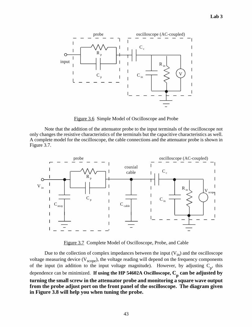
Figure 3.6 Simple Model of Oscilloscope and Probe
Note that the addition of the attenuator probe to the input terminals of the oscilloscope notonly changes the resistive characteristics of the terminals but the capacitive characteristics as well.A complete model for the oscilloscope, the cable connections and the attenuator probe is shown inFigure 3.7.
Figure 3.7 Complete Model of Oscilloscope, Probe, and Cable
Due to the collection of complex impedances between the input (Vin) and the oscilloscopevoltage measuring device (Vscope), the voltage reading will depend on the frequency componentsof the input (in addition to the input voltage magnitude). However, by adjusting Cp, this
dependence can be minimized. If using the HP 54602A Oscilloscope, Cp can be adjusted by
turning the small screw in the attenuator probe and monitoring a square wave outputfrom the probe adjust port on the front panel of the oscilloscope. The diagram givenin Figure 3.8 will help you when tuning the probe.
V
C c
C in
R in
oscilloscope (AC-coupled)probe
input
R p
C p
C c
C in
R in
oscilloscope (AC-coupled)probe
C p
R p
Cstray
coaxial cable
C cable
V inV scope

Lab 3
44
Figure 3.8 Attenuator Probe Calibration
The use of Cp to minimize the frequency dependence can be understood by looking at the
impedances in the model. To simplify the analysis we will assume that the effects of Cstray and Ccare negligible, so the impedances of the circuit sections are
(3.7)
(3.8)
(3.9)
and from voltage division, the resulting voltage input-output relationship is
(3.10)
Now it is clear that if we adjust Cp so RpCp = Rin(Cin + Ccable), the frequency dependence will beeliminated.
3.4 Specific Background Information on Using an HP54602A Oscilloscope
Looking at the front of the scope you can see that it contains a screen and a number ofbuttons and knobs. The screen displays the output of the oscilloscope. Just below the screen aresix 'soft' buttons. The function of these buttons will change depending upon menu selections. Thecurrent function of each button is displayed directly above the button on the bottom of the screen.
Overcompensated Undercompensated Calibrated
Zscope
Rin
jRinCin 1+--------------------------------=
Zscope cable+
Rin
jRin Cin Ccable+ 1+----------------------------------------------------------=
Zprobe
Rp
jRpCp 1+-----------------------------=
Vscope
Vin---------------
Zscope cable+
Zprobe Z+ scope cable+
----------------------------------------------------
Rin
jRin Cin Ccable+ 1+----------------------------------------------------------
Rp
jRpCp 1+-----------------------------
Rin
jRin Cin Ccable+ 1+----------------------------------------------------------+
----------------------------------------------------------------------------------------------= =
Lab 3
45
3.4.1 The Screen
The screen is divided into eight vertical and ten horizontal divisions. Typical informationdisplayed on the screen includes:
The Y-Axis Scale: The Y-Axis scale is located in the upper left hand corner of the screen.Each channel can have a different scale. For example if the screen reads: 1 2V 2 200mV, it meansthat channel one has a scale of 2 volts per division, while channel two has a scale of 200 millivoltsper division.
The Time Scale: The time scale is located in the upper right side of the screen. Eachchannel has the same time scale. For example, 10ms/ means 10 milliseconds per division.
Delay: The time delay indicator is located in the upper middle section of the screen. Thisdisplays whether the signal is shifted left or right. Typically this should be reading 0.00 s.
Trigger information: The current trigger mode is in the upper right hand corner of thescreen. It is displayed either as an up arrow or as a down arrow indicating positive or negativeslope triggering.
Channel Grounds: Along the right hand side of the display there will be a channel groundindicator (a ground symbol with the channel number next to it). It shows where the ground for thatchannel is with respect to the displayed grid. If the ground is off the screen there will be an arrowwith the channel number at the top or bottom of the screen to indicate where the ground is.
Along the bottom of the screen there is room for addition information to be displayed. Thevery bottom of the screen indicates the current functions of the soft buttons. These functionschange depending upon which menu button has been selected.
3.4.2 Buttons and Dials
The buttons and dials on the oscilloscope are separated into five groups: Vertical (outlinedin blue), Horizontal (outlined in gray), Trigger (outlined in green), Storage (outlined in gray) andan unnamed group (also outlined in gray). The unnamed group contains the Measure and Save/Recall sub-groups as well as the Autoscale, Display, and Print/Utility buttons.
3.4.3 Vertical
The vertical group contains four columns, one for each channel. Each column contains acoaxial input port. Above the input port is a dial labeled "Level." This dial can be used to adjustthe location of the ground on the screen. Above the "Level" knob there is a button with the channelnumber on it. Pressing this button will call up a menu that can be accessed with the soft buttonslocated just below the screen. For channels 1 and 2 this menu includes:
Off On: Selecting this will toggle the trace of the selected channel on and off
Coupling: Allows switching between AC and DC coupling.
BW Limit: Allows limiting the bandwidth of the signal displayed (helps to reduce noise).
Lab 3
46
Vernier: Leave off.
Probe: This indicates to the oscilloscope if an attenuation probe is attached. The scope willmultiply the incoming signal by the selected value before displaying it.
Channels 3 and 4 have less extensive capabilities:
Off On: Same function as channels 1 and 2
Coupling: Only DC coupling is available for channels 3 and 4
V/div: Channels three and four are limited to 2 possible voltage scales
Probe: Same as channels one and two
Between the channel 1 and channel 2 buttons, there is a button with a plus and a minus onit. This button will bring up a menu that allows you to perform math on the signals. You can add,subtract and multiply signals together or perform and display the results (spectrum) of a FastFourier Transform (FFT).
For channels 1 and 2 there is also a large green knob. This knob will change the Y-axisscale on the screen.
3.4.4 Horizontal
The horizontal control group contains one large knob (Time/Div), one small knob (Delay),and one button labeled Main/Delay. The large knob is used to adjust the time scale on the screen.This will allow you to zoom in on sections of the signal. The small knob labeled "Delay" allowsyou to move the signal left and right so you can inspect different areas of the signal. The buttonbrings up a menu that allows you to choose one of four horizontal modes and switch the locationof your time reference from the center of the screen to the left of the screen.
The four horizontal modes are:
Main: This is the normal or default setting you will usually use.
Delayed: This splits the screen vertically into two windows. On the top you will see a largesection of your signal separated by two vertical lines. On the bottom window you will see anexpanded version of the signal that lies within the two vertical lines on the upper window. Byadjusting the delay knob you can move left and right through the signal. Adjusting the Time/Divchanges the spacing between the two vertical lines and thus the amount of "zoom."
XY: This allows you to use channel 1 as the x-axis instead of time.
Roll: In this mode the scope just displays the current signal without 'trying' to maintain asteady display.
3.4.5 Trigger
Triggering ensures that the display of a signal will be stable for direct observation.

Lab 3
47
Triggering is the event that causes the scope to start scanning the electron beam creating thedisplayed signal called a trace. The scope starts the trace at the left and moves to the right at a speeddetermined by the time scale. For example, if the time scale is 200ms/division it will take the scope2 ms (200ms/division times ten divisions) to complete the trace. Once the trace has reached the endof the screen the scope waits for another triggering event to initiate the trace again. The triggeringevent can be adjusted by the knobs and buttons in the trigger menu.
The trigger group contains two knobs and three buttons:
Source: This button allows you to choose which channel will be used as the trigger. Inaddition to the four input channels, the line can also be used as a trigger. This means the scope willtrigger based on the voltage coming from the AC power source. This is useful when looking fornoise caused by electrical interference.
Mode: You should usually select the normal mode
Slope/Coupling: This button will bring up a menu that allows you to select the slope of thetrigger. You can either trigger on the signal when it is going up or going down (up arrow, downarrow) depending on how you want the signal displayed. This menu also contains features that willhelp you trigger on a noisy signal
Level: This knob allows you to adjust the voltage level at which triggering occurs.Combined with the slope this is how triggering is adjusted. For example, if you have the level setto zero and the slope set to + (up arrow) you will be triggering every time the signal goes frombelow zero volts to above zero volts. The level is very important when you are dealing with signalsthat have been rectified (by a diode). A rectified signal may never have a value of less than zero,and if you leave the level at zero, the scope may never trigger, and no signal will be displayed.
Holdoff: You should not need to use this.
3.4.6 Storage
The scope has the ability to store signals for later display and comparison.
3.4.7 Measure
There are three buttons and some knobs in the measure sub-group:
Voltage: pressing this button brings up a menu that will allow you to make a variety ofvoltage measurements.
By selecting the appropriate soft button you can display just about any information that youwant. For example, if you want to know the RMS voltage of the signal on channel 2, you shouldpush the left-most soft button until the number 2 is highlighted and then press the Vrms button.The RMS voltage will appear near the bottom of the screen.
Time: Similar to the voltage button, this displays a menu that will allow you to make avariety of time measurements. You can measure frequency, period, rise time, etc.
Cursors: This button allows you to make manual measurements of a signal. It will bring up

Lab 3
48
a window with the following options.
Source: Allows you to change the channel you are measuring.
Active Cursor: You will be able to have four cursors on the screen at once. Two are verticallabeled V1 and V2, and two are horizontal labeled T1 and T2. Using the unlabeled knob just belowand to the right of the cursors button you will be able to move the active cursor around. While youare moving the cursor the screen will display its position relative to ground (or zero time) and alsorelative to the other cursor. This allows you to measure the voltage difference for any specific partof the signal.
3.4.8 Save/Recall
This group contains two buttons:
Trace: This allows you to save a trace so you can look at it later.
Setup: This button brings up a menu that allows you to save the setup of your voltage andtime scales as well as your triggering. This may be useful if you have a particular setup you like.Also in this menu is an Undo Autoscaling button that will be useful if you press the Autoscalebutton by accident and lose your signal.
Autoscale
This is probably the most useful button on the scope. Pressing this button willautomatically setup the voltage scales, time scale, and triggering so you produce a stable display.Although it is very helpful, it is not perfect for every application. It is easy to overuse this button.Here are some things to watch out for:
(1) If you have a relatively low frequency signal (less than 50 Hz) Autoscale will not findthe signal.
(2) If you have a DC signal, Autoscale may not find the signal. If so, try switching yourtrigger source to line if you cannot get a DC signal displayed.
(3) If you are using more than one channel Autoscale will set the vertical scalesdifferently and adjust the ground levels so each signal is displayed separately.
Display
This button will bring up a menu with the following options:
Display Mode [normal, peak detect, average]: Leave this on normal
Vernier: Leave this off
Grid: Pressing this will let you turn the grid on and off

Lab 3
49
3.4.9 How to Find a Signal on an HP54602A Oscilloscope
Use the following procedure to display an unknown input signal on the oscilloscope:
(1) Optional: It is a good practice to reset the settings of the scope to default settingsbefore beginning because you might not know what state the scope was left in byprevious users. To do this, press the "Setup" buton in the "Save/Recall" button group.Then select "Default Setup" with the below-screen button.
(2) First try pressing the Autoscale button. Often this will automatically scale anddisplay the signal. If the signal is not displayed (e.g., when a signal has a lowfrequency or is dc), continue with the remaining steps below.
(3) Make sure the desired channel is on and set up properly.
• Press the number button corresponding to the channel you want to observe
• Turn the channel on by pressing the left-most "soft" button.
• With the right-most 'soft' button, select the type of probe you are using.
• If it is possible that your signal could have a large DC offset, select AC couplingwith the second-to-left below-screen button. This will remove the DC offset andbring the pure AC portion of the signal into range.
• Make sure BW Lim, Invert, and Vernier are off.
(4) Move the channel ground to the center of the display.
• There should be a ground symbol on the right hand side of the screen.
• If the ground is off the screen there will be an arrow in either the upper or lowerright hand corner pointing to it.

Lab 3
50
(5) You can move the ground up and down with the small, light colored, “position” knob.Make sure the trigger is set up correctly.
• Press the 'source' button and then select the appropriate channel
• Press the 'mode' button and select "Auto Lvl"
• Adjust the level knob until the level is within the range of the signal
• If you have a noisy signal press the Slope/Coupling button and turn the "Noise Rej"on.
(6) Set the Vertical scale.
• The vertical scale is displayed in the upper left corner of the screen
• Turn the Volts/Div knob (above Channel 1) until the vertical scale is about half ofthe amplitude of the signal.
(7) Set the Time scale.
• The time scale is displayed at the top of the screen (just right of center)
• Turn the Time/Div knob until the time scale is about ½ of the period of the signal.

Lab 3
51
3.5 Laboratory Procedure / Summary Sheet
Group: ____ Names: _________________________ _____________________________
_________________________ _____________________________
(1) In this step you will examine the effects of AC coupling of an oscilloscope.
Set the function generator to produce a 5 Vpp 1kHz sinusoidal output. To do this,press the Vpp button, enter 5, and press Enter. The "Not Entered" light should go offwhen you press Enter; otherwise, press it again more firmly and squarely.
Display the sinusoid on the oscilloscope with a sensitivity of 1 V/div. Make sure thetriggering source is set to the proper "channel" (and not "line" triggering). NOTE -If using the Philips PM5193 function generator, be sure to connect to the lower“OUTPUT” jack (not the upper “TTL OUT” jack).
Adjust the triggering level and notice what effect it has.
Use the +/– trigger selector (press the slope button and toggle between positive andnegative edge triggering) and notice what effect it has.
Refer back to Figure 3.2 for details on the impedances within the oscilloscope. Wecan simulate an AC coupled oscilloscope by adding an external coupling capacitor toa DC coupled oscilloscope. To do this, build the circuit shown in Figure 3.9. Usingthe function generator Vdc button, add a 5 Vdc offset to the 5Vpp 1kHz signal (byentering 5 and pressing Enter).
Be sure to select DC coupling on the oscilloscope. Use a 0.022 F coupling capacitor(Ccoupling) and note the resulting output. Then try a 0.1 F and a 1 F capacitor (referback to Section 1.4 in Lab 1 for info on how to read capacitor values). Note carefullywhat happens to the oscilloscope display when you first attach the scope 1Xprobe (or banana cable with alligator clip) to measure Vo for each case. Make
sure you discharge the coupling capacitor by shorting its leads before you attach theprobe to measure the voltage. How do the results change with the capacitance value?
What is the effect of the function generator output impedance Ro on the measuredvoltage Vo?
Now remove the coupling capacitor and toggle the oscilloscope between DC couplingand AC coupling and note what you observe in the measured voltage signal. Whichof the three external coupling capacitors that you tried most closely approximateswhat you think the actual coupling capacitance of the oscilloscope is?
Lab 3
52
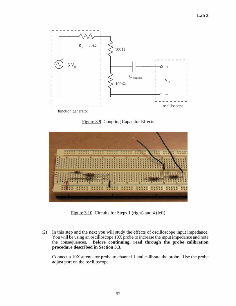
Figure 3.9 Coupling Capacitor Effects
Figure 3.10 Circuits for Steps 1 (right) and 4 (left)
(2) In this step and the next you will study the effects of oscilloscope input impedance.You will be using an oscilloscope 10X probe to increase the input impedance and notethe consequences. Before continuing, read through the probe calibrationprocedure described in Section 3.3.
Connect a 10X attenuator probe to channel 1 and calibrate the probe. Use the probeadjust port on the oscilloscope.
V o
+
R o 50
100
function generatoroscilloscope
C coupling
5 Vpp +
100
Lab 3
53
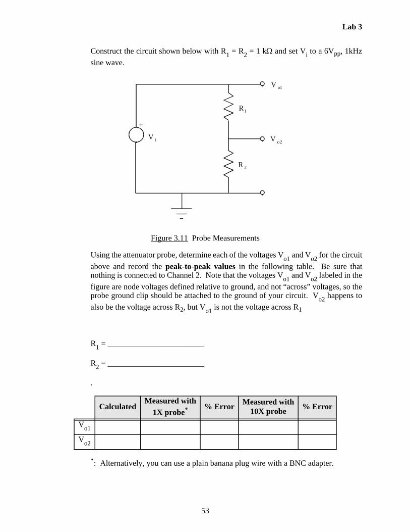
Construct the circuit shown below with R1 = R2 = 1 k and set Vi to a 6Vpp, 1kHz
sine wave.
Figure 3.11 Probe Measurements
Using the attenuator probe, determine each of the voltages Vo1 and Vo2 for the circuit
above and record the peak-to-peak values in the following table. Be sure thatnothing is connected to Channel 2. Note that the voltages Vo1 and Vo2 labeled in the
figure are node voltages defined relative to ground, and not “across” voltages, so theprobe ground clip should be attached to the ground of your circuit. Vo2 happens to
also be the voltage across R2, but Vo1 is not the voltage across R1
R1 = ________________________
R2 = ________________________
.
*: Alternatively, you can use a plain banana plug wire with a BNC adapter.
CalculatedMeasured with
1X probe* % ErrorMeasured with
10X probe% Error
Vo1
Vo2
+
R1
R 2
V i
V o1
V o2
Lab 3
54
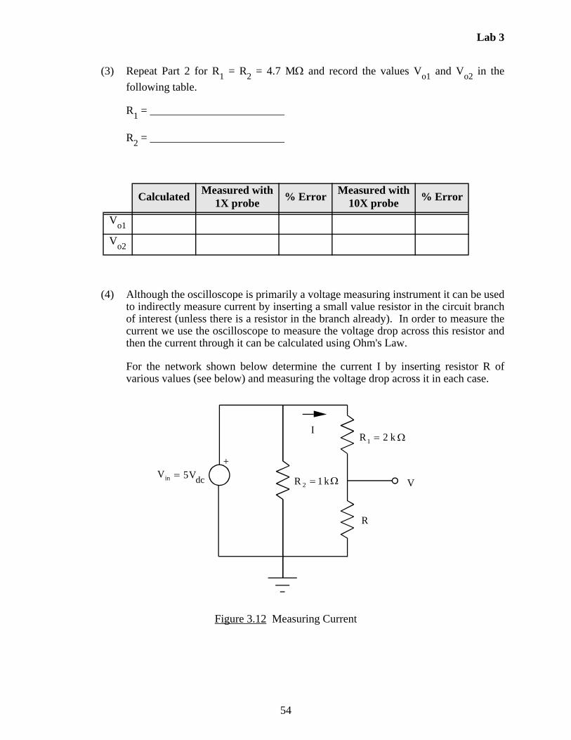
(3) Repeat Part 2 for R1 = R2 = 4.7 M and record the values Vo1 and Vo2 in the
following table.
R1 = ________________________
R2 = ________________________
(4) Although the oscilloscope is primarily a voltage measuring instrument it can be usedto indirectly measure current by inserting a small value resistor in the circuit branchof interest (unless there is a resistor in the branch already). In order to measure thecurrent we use the oscilloscope to measure the voltage drop across this resistor andthen the current through it can be calculated using Ohm's Law.
For the network shown below determine the current I by inserting resistor R ofvarious values (see below) and measuring the voltage drop across it in each case.
Figure 3.12 Measuring Current
CalculatedMeasured with
1X probe% Error
Measured with10X probe
% Error
Vo1
Vo2
+
R1 2 k
R 2 1 k VVin 5V
R
I
dc

Lab 3
55
Record the exact (measured) resistance values for R1 and R2:
R1 = ________________________
R2 = ________________________
For each resistance value below, measure the voltage (V) across resistor R. NOTE - whenmeasuring small voltages with the oscilloscope, you might need to adjust the voltage scalemanually to get accurate readings.
Record the exact (measured) resistance values for each of the three R resistors used:
R (10 ) = ________________________
R (100 ) = ________________________
R (1 k) = ________________________
Calculate the expected current through R (for each value) using the actual values for R1 andR. Then calculate currents from the measured voltage values above (using Ohm’s Law), andcompare them to the expected current values:
RMeasured with
1X probeMeasured with
10X probe
10 100 1 K
Rexpected
(calculated) current
I via the1X probe
measurement% Error
I via the10X probe
measurement% Error
10 100 1 K

Lab 3
56
LAB 3 QUESTIONS
Group: ____ Names: _________________________ _____________________________
_________________________ _____________________________
(1) From the data obtained for Vo2 in step 3 of the procedure, determine the input impedance
of the oscilloscope with the 10X attenuator probe attached (see Section 2.2.8 in Lab 2).
(2) How does the input impedance of the oscilloscope with the 10X attenuator probe compareto the input impedance with the 1X probe?
(3) By what factor is the input voltage attenuated when the 10X probe is used with theoscilloscope?
(4) When is it advantageous to use the oscilloscope attenuator probe?

Lab 3
57
(5) You have a 4 Vpp, 100 Hz sine wave, and I wish it to be displayed on the oscilloscope asshown below. Indicate what values to set for the vertical amplifier (voltage divisions), timebase, and trigger.
Figure 3.13 Oscilloscope Sine Wave Display
(6) What is the effect of AC coupling when a signal with a DC offset is displayed on anoscilloscope?
(7) In part 4, what effect does the inserted resistor have on the current measured?

Lab 3
58
Lab 4
59
Laboratory 4
Bandwidth, Filters, and Diodes
Required Components:• 1 1k resistor• 1 0.1F capacitor• 1 1N914 small-signal diode• 1 LED
4.1 Objectives
In the previous laboratory exercise you examined the effects of input and outputimpedances of instruments on signals and measurements. In this laboratory exercise you will studythe bandwidth, which is another important signal, circuit, and instrument characteristic. You willbuild basic filter circuits and determine the range of frequencies that they affect.
You will also use semiconductor diodes and light emitting diodes (LED) and build basiccircuits that require these components.
4.2 Introduction
Ideally an instrument with purely resistive input terminal characteristics should be able tofaithfully reproduce any input of any frequency. However, real instruments also have capacitanceand inductance which affect the quality of signal reproduction. With real instruments the range offrequencies over which the input is faithfully reproduced is limited, quite often severely, by suchfactors as reactance (capacitance or inductance) in electrical systems, and inertia and damping inmechanical systems.
In order to quantify the range of frequencies a system can reproduce, the term bandwidthis used. The bandwidth of a system is defined as: the range of frequencies for which the amplitudeof the input of the system is attenuated not more than 3 dB. This is equivalent to 70.7% of itsoriginal value. The frequency at which the gain of the system drops below 3 dB is defined as acorner or cutoff frequency c.
The bandwidth of a deterministic electrical system can be readily determined analyticallyby writing the transfer function and solving for the corner frequency as is done below for theexample circuit shown in Figure 4.1.
Lab 4
60
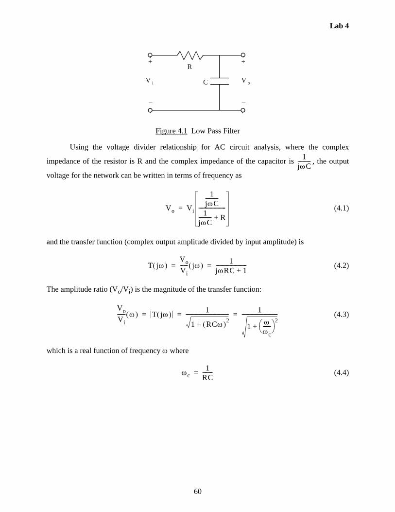
Figure 4.1 Low Pass Filter
Using the voltage divider relationship for AC circuit analysis, where the complex
impedance of the resistor is R and the complex impedance of the capacitor is , the output
voltage for the network can be written in terms of frequency as
(4.1)
and the transfer function (complex output amplitude divided by input amplitude) is
(4.2)
The amplitude ratio (Vo/Vi) is the magnitude of the transfer function:
(4.3)
which is a real function of frequency where
(4.4)
V i V o
R
C
+ +
––
1jC----------
Vo Vi
1jC----------
1jC---------- R+---------------------=
T j Vo
Vi------ j 1
jRC 1+------------------------= =
Vo
Vi------ T j 1
1 RC 2+--------------------------------- 1
1c------ 2
+
----------------------------= = =
c1
RC--------=
Lab 4
61
Note the following:
as , (4.5)
as , (4.6)
as , (4.7)
Therefore, c is the corner or cutoff frequency. This frequency, in Hertz, is
(4.8)
The bandwidth of this circuit is:
(4.9)
which implies that this circuit passes low frequencies only which is why it is called a low-passfilter.
In order to experimentally determine the bandwidth of a circuit it is necessary to drive thecircuit with signals having a range of frequencies. Measuring the output over the input as afunction of frequency determines the frequency response of the system. The bandwidth is foundby finding the 3 dB points of the frequency response curve. If there are two cutoff points, thebandwidth is written as:
(4.10)
To determine the bandwidth of the circuits used in this laboratory exercise you will be usingthe frequency sweep feature of a function generator, as described in the next section.
0Vo
Vi------ 1
Vo
Vi------ 0
cVo
Vi------ 1
2------- 0.707 3 dB–= =
fc
c
2------ 1
2RC---------------= =
0 c
clow chigh
Lab 4
62
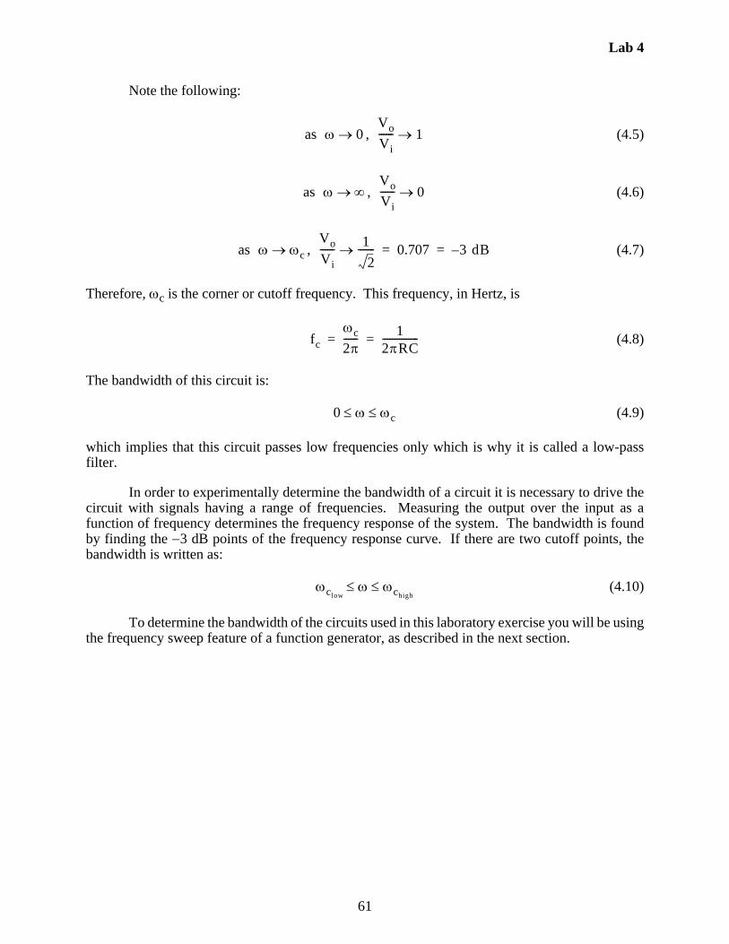
4.3 Using a Frequency Sweep Feature on a Function Genrator
This section outlines a procedure to generate a frequency sweep, which is a signal of aspecific waveform (e.g., a sine or square wave) whose frequency increases in a step-wise fashionfrom a selected start frequency to another selected stop frequency as shown in Figure 4.2. If afrequency sweep is used as an input to a circuit (e.g., a low pass filter circuit), the resulting outputwould will illustrate the frequency response of the circuit as shown in Figure 4.3. The cutofffrequency (fc) can be found by estimating where the amplitude reaches 0.707 of the initialamplitude. Below are procedures for using frequency sweeps with both virtual instruments andtypical desktop equipment.
Figure 4.2 Frequency Sweep
Figure 4.3 Sweep Frequency Response
NI ELVIS Procedure:
One way to do a sweep is to just manually select individual input frequencies on thefunction generator without using the sweep function. Start with a low frequency (e.g., 1 Hz) andgradually increment the frequency (with the same amplitude) until the output amplitude on theoscilloscope reduces to 0.707 of the input value. This is the recommended method in this Labusing the NI ELVIS.
fstart fstop
fstart fstop
1
0.707
fc

Lab 4
63
Alternatively, you can set up an automatic sweep and interupt the sweep manually whenthe output amplitude reaches the 0.707 level. To do it this way:
On the function generator:
(1) Select "sine wave" for the waveform type.
(2) Input a "start" frequency 1 Hz.
(3) Input a "stop" frequency 4000 Hz.
(4) Input the amplitude (1V) or peak-to-peak voltage (2Vpp).
(5) Set the DC offset (Vdc) to 0.
(6) Select the step interval to 20ms.
(7) Select the step size to 10 Hz. This will result in a total sweep time of about 8 s (4000Hz / 10 Hz * 0.02 s)
On the oscilloscope:
(1) Attach the probe to the output and select "immediate."
(2) Click "run" on the oscilloscope and then "sweep" (not "run") on the functiongenerator, and wait for the Vpp to be about 1.414 V, then click "stop."
(3) Read and record the corresponding frequency. (If the frequency did not appear, tryagain after setting more appropriate values for volts/div and time/div.)
Philips PM5193 Programmable Function Generator Procedure:
The frequency is controlled by a voltage-controlled oscillator in the instrument. Thevoltage that corresponds to the frequency is available at the SWEEP output on the back of theinstrument.
(1) Choose the type of waveform you desirePush the "sine wave" button on the keypad labeled "Wave Form."
(2) Select the "start" frequencyPress the "start" button on the keypad labeled "Frequency." Then type in thenumerical value of 1. If Hz is not indicated, press the Hz/kHz button to indicate Hz.Do not press ENTER until step 7!
(3) Select the "stop" frequencyPress the "stop" button to the right of the "start" button. Now type in the value of4000, again making sure that Hz is indicated.

Lab 4
64
(4) Select the amplitude or peak-to-peak voltagePress the "Vpp" button on the "Level" keypad. Then enter a value of 2 to result in anamplitude of 1.
(5) Set the DC offsetPress the "Vdc" button and enter 0.
(6) Select the sweep timePress the "Time(s)" button under "Modulation" and enter 10 milliseconds (0.01 s).
(7) Activate the parametersPress the orange "enter" button at the far right of the function generator.
(8) Activate the line sweepPress the "lin sweep" button on the "Modulation" keypad. Within 4 seconds ofpressing the button, enter 1 on the keypad to select the appropriate mode. Then pressthe "cont" button to continuously repeat the sweep defined by the parameters above.In order to change any of the parameters, press the "single" button, change theparameter as indicated above, and press the "cont" button to resume the continuouslyrepeating sweep.
Use the following steps to generate a frequency response display on the oscilloscope:
(1) Set the time and voltage scales to appropriate valuesSet the time base of the scope to match the sweep time, in this case 2 ms/div. Thenselect an amplitude/division value (e.g., 5 V/div) that will fit the entire waveform onthe display.
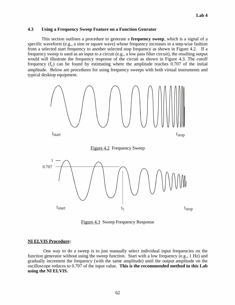
(2) Use the sweep signal as the triggerConnect the SWEEP output on the back of the PM5193 (not the TTL or regularoutputs on the front) to CH2 of the oscilloscope with its vertical scale set at 5 V/div.This is a stepped triangular waveform that controls the frequency sweep (see Figure4.4). Select Norm Trigger, CH2, -slope, and internal source to trigger off the fallingedge of the triangle waveform. To better view the full frequency response, place thefirst step of the triangle on the 2nd division on the scope and the last step on the 7thdivision (see Figure 4.4). With the parameters defined above, 5 horizontal divisions(2 ms/div) correspond to the sweep time of the signal.
Lab 4
65
Figure 4.4 Function Generator Sweep Signal
(3) View the swept frequency signalConnect the output of the PM5193 to CH1 of the scope. Be careful not to change thetriggering from the SWEEP on CH2. You should see a waveform similar to thatshown in Figure 4.2.
(4) View the frequency response of a circuitConnect the function generator output to the circuit input and connect the circuitoutput to CH1 of the scope. The cutoff frequency (fc) can be found by estimatingwhere the amplitude reaches 0.707, and by determining the frequency value thatcorresponds to that point in the sweep. For example, if cutoff point is at 1/5th of thedistance from the start of the sweep to the end, fc would be 800 Hz (4000 Hz / 5).You can count the number of steps in the function-generator sweep output to helpestimate the fraction (e.g., 2 steps out of 10 would be 1/5). You can also use theoscilloscope cursors to help in estimating the cutoff frequency.
2nd div 7th div
sweep time
trigger edge
10 ms

Lab 4
66
Lab 4
67
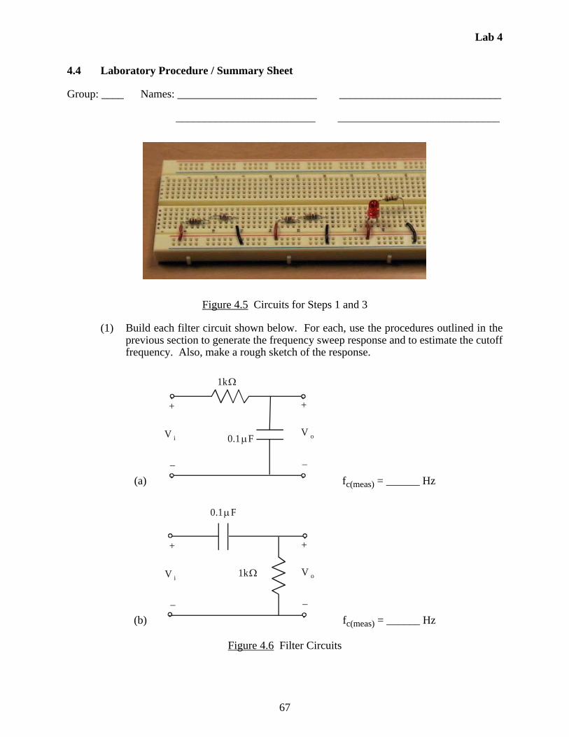
4.4 Laboratory Procedure / Summary Sheet
Group: ____ Names: _________________________ _____________________________
_________________________ _____________________________
Figure 4.5 Circuits for Steps 1 and 3
(1) Build each filter circuit shown below. For each, use the procedures outlined in theprevious section to generate the frequency sweep response and to estimate the cutofffrequency. Also, make a rough sketch of the response.
(a) fc(meas) = ______ Hz
(b) fc(meas) = ______ Hz
Figure 4.6 Filter Circuits
V iV o
+ +
––
1k
0.1F
V iV o
+ +
––
1k
0.1F
Lab 4
68
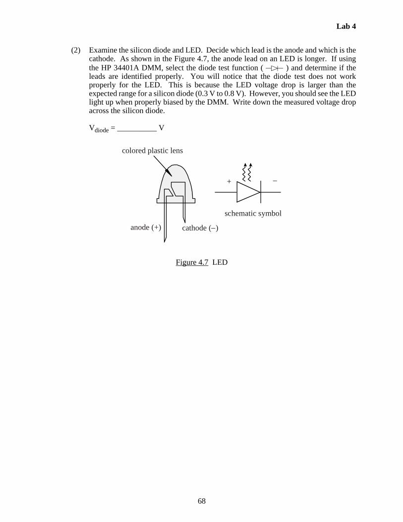
(2) Examine the silicon diode and LED. Decide which lead is the anode and which is thecathode. As shown in the Figure 4.7, the anode lead on an LED is longer. If usingthe HP 34401A DMM, select the diode test function ( ) and determine if theleads are identified properly. You will notice that the diode test does not workproperly for the LED. This is because the LED voltage drop is larger than theexpected range for a silicon diode (0.3 V to 0.8 V). However, you should see the LEDlight up when properly biased by the DMM. Write down the measured voltage dropacross the silicon diode.
Vdiode = __________ V
Figure 4.7 LED
+
colored plastic lens
anode (+) cathode ( )
schematic symbol
Lab 4
69
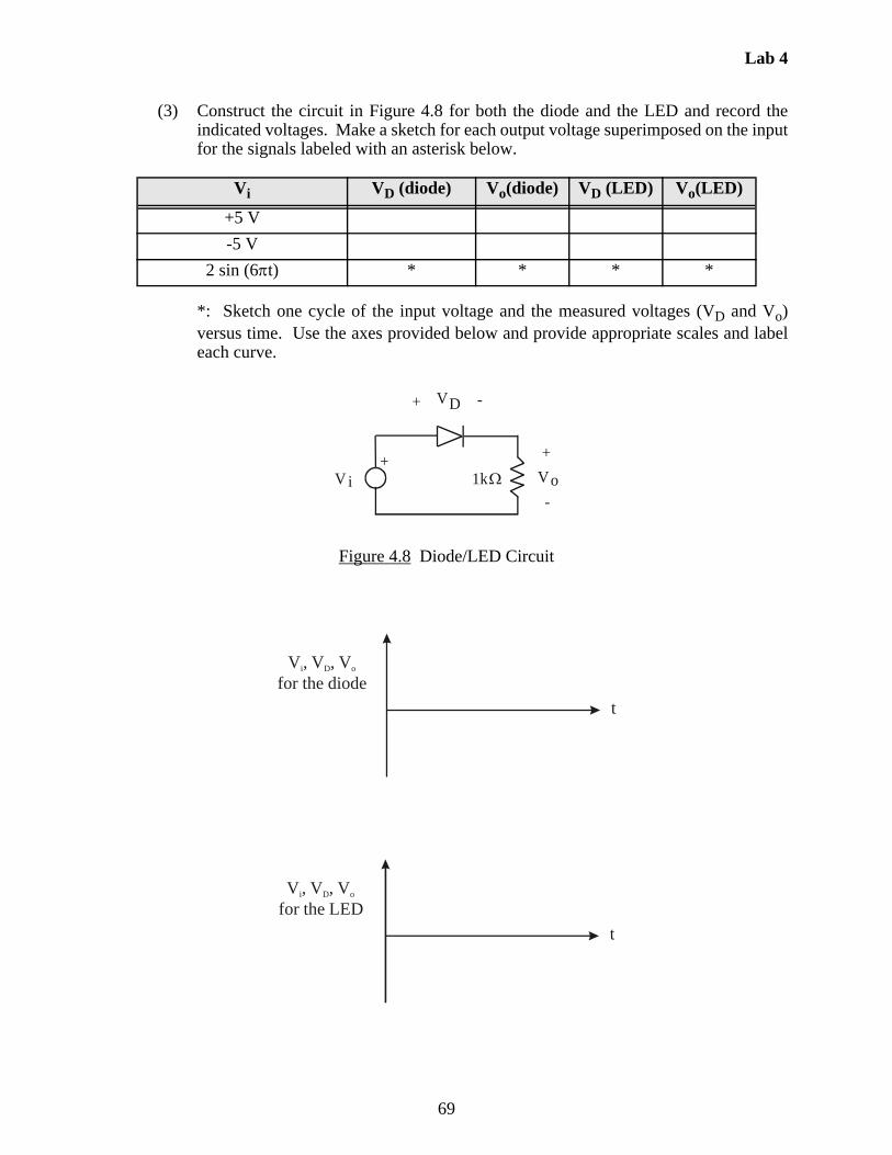
(3) Construct the circuit in Figure 4.8 for both the diode and the LED and record theindicated voltages. Make a sketch for each output voltage superimposed on the inputfor the signals labeled with an asterisk below.
*: Sketch one cycle of the input voltage and the measured voltages (VD and Vo)versus time. Use the axes provided below and provide appropriate scales and labeleach curve.
Figure 4.8 Diode/LED Circuit
Vi VD (diode) Vo(diode) VD (LED) Vo(LED)
+5 V
-5 V
2 sin (6t) * * * *
+Vi 1k
VD+ -
Vo
+
-
t
V , V , Vfor the diode
i D o
t
V , V , Vfor the LED
i D o

Lab 4
70
LAB 4 QUESTIONS
Group: ____ Names: _________________________ _____________________________
_________________________ _____________________________
(1) For the circuit in Step 1a:
what type of filter is this? ____________
Also, calculate the theoretical cutoff frequency and the percent error in your measuredvalue:
c(meas) = ________ c(theor) = ________ % error = ________
Remember that = 2f.
(2) For the circuit in Step 1b, derive expressions for the magnitude ratio of the frequencyresponse and for the cutoff frequency (c).
c =
what type of filter is this? ____________
Vo
Vi------

Lab 4
71
Also, calculate the theoretical cutoff frequency and the percent error in your measuredvalue:
c(meas) = ________ c(theor) = ________ % error = ________
(3) In step 3, if the diode where removed and replaced in the opposite direction in the circuit,what effect would this have on the outputs for the sine wave input?

Lab 4
72
Lab 5
73
Laboratory 5
Transistor and Photoelectric Circuits
Required Components:• 1 330 resistor• 2 1 k resistors• 1 10k resistor• 1 2N3904 small signal transistor• 1 TIP31C power transistor• 1 1N4001 power diode• 1 Radio Shack 1.5-3V DC motor (RS part number: 273-223)• 1 LED• 1 photodiode/phototransistor pair (Digikey part number: H21A1QT-ND)
5.1 Objectives
In this laboratory, you will study bipolar junction transistors (BJTs) and commonphotoelectric components. You will learn how to use light-emitting diodes (LEDs) as indicators,switch an inductive load with a power BJT, and use LED and phototransistor pairs as photo-interrupters. You will also learn how to bias a transistor and how to provide flyback protection witha diode.
5.2 Introduction
The following two pages provide information from the 2N3904 transistor data sheet. Datasheets provide pin-out information, where each pin is labeled with a function name and, ifappropriate, a number. A data sheet also provides detailed electrical specifications that can helpyou properly design a circuit using the component.
Figure 5.1 illustrates the nomenclature used to describe the behavior of an npn bipolartransistor. It is a three terminal device consisting of the base, collector, and emitter. The transistoracts like a current valve by using the voltage bias across the base and emitter (VBE) to control theflow of current in the collector-emitter circuit (IC). The circuit connected to the collector andemitter along with the bias voltage dictate how much current flows.

Lab 5
74
CB E
TO-92
C
B
E
BC
C
SOT-223
E
NPN General Purpose AmplifierThis device is designed as a general purpose amplifier and switch.The useful dynamic range extends to 100 mA as a switch and to100 MHz as an amplifier.
Absolute Maximum Ratings* TA = 25°C unless otherwise noted
*These ratings are limiting values above which the serviceability of any semiconductor device may be impaired.
NOTES:1) These ratings are based on a maximum junction temperature of 150 degrees C.2) These are steady state limits. The factory should be consulted on applications involving pulsed or low duty cycle operations.
Symbol Parameter Value UnitsVCEO Collector-Emitter Voltage 40 VVCBO Collector-Base Voltage 60 VVEBO Emitter-Base Voltage 6.0 VIC Collector Current - Continuous 200 mA
TJ, Tstg Operating and Storage Junction Temperature Range -55 to +150 °C
Thermal Characteristics TA = 25°C unless otherwise noted
Symbol Characteristic Max Units2N3904 *MMBT3904 **PZT3904
PD Total Device DissipationDerate above 25°C
6255.0
3502.8
1,0008.0
mWmW/°C
RθJC Thermal Resistance, Junction to Case 83.3 °C/WRθJA Thermal Resistance, Junction to Ambient 200 357 125 °C/W
*Device mounted on FR-4 PCB 1.6" X 1.6" X 0.06."
**Device mounted on FR-4 PCB 36 mm X 18 mm X 1.5 mm; mounting pad for the collector lead min. 6 cm2.
2N3904 MMBT3904
SOT-23Mark: 1A
PZT3904
2N3904 / M
MB
T3904 / PZT3904
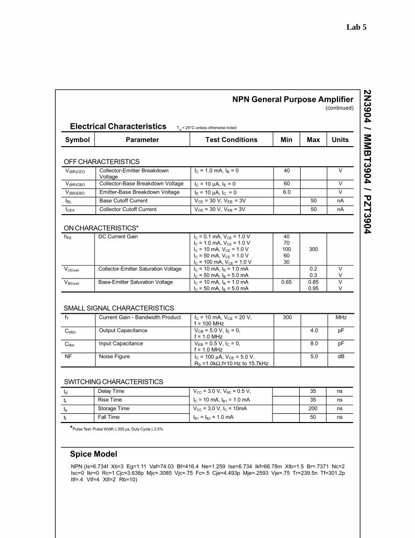
Lab 5
75
Electrical Characteristics TA = 25°C unless otherwise noted
Symbol Parameter Test Conditions Min Max Units
V(BR)CEO Collector-Emitter BreakdownVoltage
IC = 1.0 mA, IB = 0 40 V
V(BR)CBO Collector-Base Breakdown Voltage IC = 10 μA, IE = 0 60 VV(BR)EBO Emitter-Base Breakdown Voltage IE = 10 μA, IC = 0 6.0 VIBL Base Cutoff Current VCE = 30 V, VEB = 3V 50 nAICEX Collector Cutoff Current VCE = 30 V, VEB = 3V 50 nA
OFF CHARACTERISTICS
ON CHARACTERISTICS*
SMALL SIGNAL CHARACTERISTICS
SWITCHING CHARACTERISTICS
*Pulse Test: Pulse Width ≤ 300 μs, Duty Cycle ≤ 2.0%
NPN (Is=6.734f Xti=3 Eg=1.11 Vaf=74.03 Bf=416.4 Ne=1.259 Ise=6.734 Ikf=66.78m Xtb=1.5 Br=.7371 Nc=2Isc=0 Ikr=0 Rc=1 Cjc=3.638p Mjc=.3085 Vjc=.75 Fc=.5 Cje=4.493p Mje=.2593 Vje=.75 Tr=239.5n Tf=301.2pItf=.4 Vtf=4 Xtf=2 Rb=10)
Spice Model
fT Current Gain - Bandwidth Product IC = 10 mA, VCE = 20 V,f = 100 MHz
300 MHz
Cobo Output Capacitance VCB = 5.0 V, IE = 0,f = 1.0 MHz
4.0 pF
Cibo Input Capacitance VEB = 0.5 V, IC = 0,f = 1.0 MHz
8.0 pF
NF Noise Figure IC = 100 μA, VCE = 5.0 V,RS =1.0kΩ,f=10 Hz to 15.7kHz
5.0 dB
td Delay Time VCC = 3.0 V, VBE = 0.5 V, 35 ns
tr Rise Time IC = 10 mA, IB1 = 1.0 mA 35 ns
ts Storage Time VCC = 3.0 V, IC = 10mA 200 ns
tf Fall Time IB1 = IB2 = 1.0 mA 50 ns
hFE DC Current Gain IC = 0.1 mA, VCE = 1.0 VIC = 1.0 mA, VCE = 1.0 VIC = 10 mA, VCE = 1.0 VIC = 50 mA, VCE = 1.0 VIC = 100 mA, VCE = 1.0 V
40701006030
300
VCE(sat) Collector-Emitter Saturation Voltage IC = 10 mA, IB = 1.0 mAIC = 50 mA, IB = 5.0 mA
0.20.3
VV
VBE(sat) Base-Emitter Saturation Voltage IC = 10 mA, IB = 1.0 mAIC = 50 mA, IB = 5.0 mA
0.65 0.850.95
VV
2N3904 / M
MB
T3904 / PZT3904
NPN General Purpose Amplifier(continued)

Lab 5
76
Figure 5.1 npn Bipolar Transistor Symbol and Nomenclature
Here are some general relationships between the variables shown in Figure 5.1:
(5.1)
(5.2)
(5.3)
Also, generally,
(5.4)
When the transistor is in saturation (i.e., fully ON),
, , and (5.5)
and when the transistor is in its cutoff state,
and (5.6)
In the cutoff state, the transistor does not conduct current.
base
collector
emitter
VB
VC
VE
VCE
+
-VBE
+
-
IC
IE
IB
VBE VB VE–=
VCE VC VE–=
IE IB IC+=
VC VE
VBE 0.6V to 0.7V VCE 0.2V IC >> IB
VBE 0.6V IB IC IE 0= = =
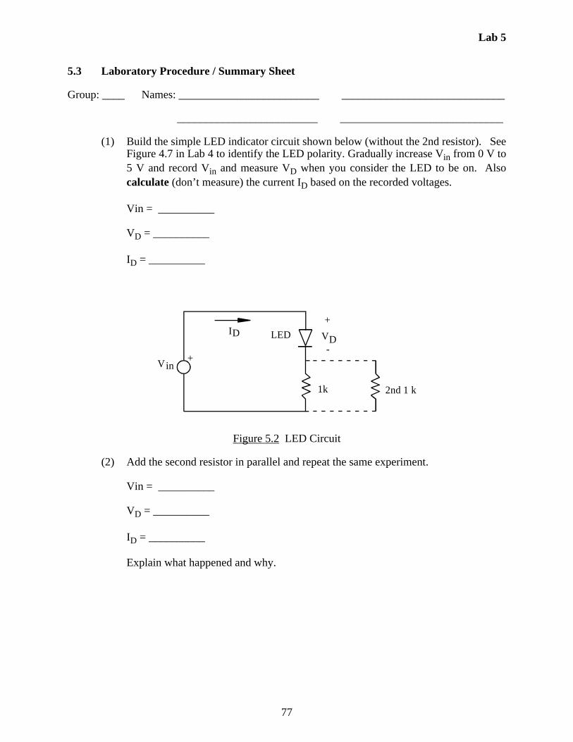
Lab 5
77
5.3 Laboratory Procedure / Summary Sheet
Group: ____ Names: _________________________ _____________________________
_________________________ _____________________________
(1) Build the simple LED indicator circuit shown below (without the 2nd resistor). SeeFigure 4.7 in Lab 4 to identify the LED polarity. Gradually increase Vin from 0 V to5 V and record Vin and measure VD when you consider the LED to be on. Alsocalculate (don’t measure) the current ID based on the recorded voltages.
Vin = __________
VD = __________
ID = __________
Figure 5.2 LED Circuit
(2) Add the second resistor in parallel and repeat the same experiment.
Vin = __________
VD = __________
ID = __________
Explain what happened and why.
+Vin
ID LED VD
1k
+
-
2nd 1 k

Lab 5
78
(3) Build a simple transistor switch (see figure below) using a 2N3904 small signaltransistor and a base resistor (RB) of 1 k. Use the variable voltage power supply orthe function generator dc output for Vin so it can be adjusted later in small increments.Use the DC power supply for the 10V source.
Figure 5.3 Transistor Switch
Use the 2N3904 datasheet provided in Section 5.2 to help you draw and label thepins on the figure below and to record the following values:
maximum allowed IC = __________ maximum allowed VCE = _____________
minimum required VBE for saturation = ____________
Figure 5.4 2N3904 Pin-out
Vin
RB
1 k
VCE
VBE
+
-+
-
10 V
IC

Lab 5
79
Vary Vin as indicated in the table below and record the associated values for VBE andVCE. Use RB = 1 k for the base resistor
Describe your conclusions about when saturation occurs for the transistor.
Change the base resistor (RB) to 10 k and repeat the measurements.
What is the effect of a larger base resistor? Why?
Vin VBE VCE
0.0
0.4
0.5
0.6
0.7
0.8
0.9
1.0
Vin VBE VCE
0.0
0.4
0.5
0.7
0.9
1.1
1.3
1.5
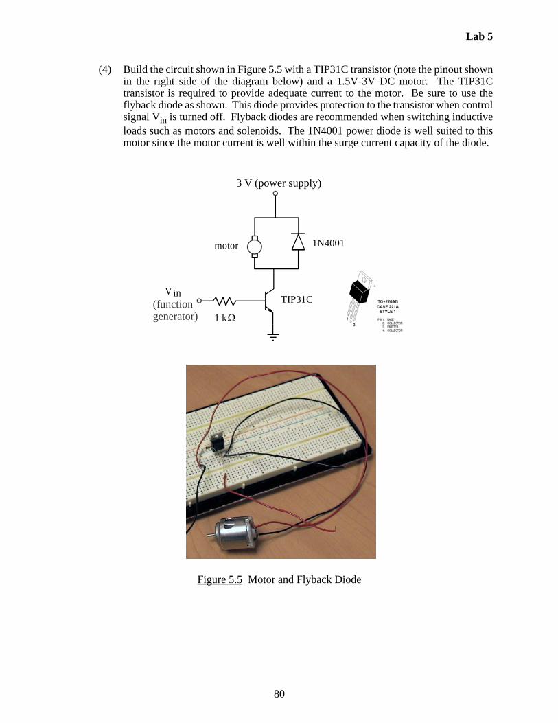
Lab 5
80
(4) Build the circuit shown in Figure 5.5 with a TIP31C transistor (note the pinout shownin the right side of the diagram below) and a 1.5V-3V DC motor. The TIP31Ctransistor is required to provide adequate current to the motor. Be sure to use theflyback diode as shown. This diode provides protection to the transistor when controlsignal Vin is turned off. Flyback diodes are recommended when switching inductiveloads such as motors and solenoids. The 1N4001 power diode is well suited to thismotor since the motor current is well within the surge current capacity of the diode.
Figure 5.5 Motor and Flyback Diode
3 V (power supply)
TIP31C
motor 1N4001
1 k
Vin(functiongenerator)

Lab 5
81
Gradually increase Vin from 0 V to 5 V and describe what happens.
Apply a 5Vpp, 2.5V dc offset (0 to 5V) square wave input to Vin. Start with a lowfrequency (e.g., 1 Hz) and then try some higher frequencies, increasing the frequencyin 1 Hz increments up to 20 Hz and then 10 Hz increments up to 100 Hz. Describewhat happens to the motor.
Explain how the flyback diode works.
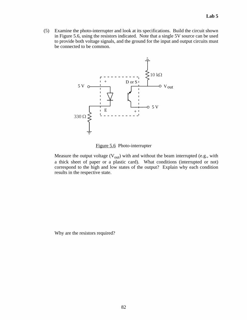
Lab 5
82
(5) Examine the photo-interrupter and look at its specifications. Build the circuit shownin Figure 5.6, using the resistors indicated. Note that a single 5V source can be usedto provide both voltage signals, and the ground for the input and output circuits mustbe connected to be common.
Figure 5.6 Photo-interrupter
Measure the output voltage (Vout) with and without the beam interrupted (e.g., witha thick sheet of paper or a plastic card). What conditions (interrupted or not)correspond to the high and low states of the output? Explain why each conditionresults in the respective state.
Why are the resistors required?
+
+E
D or S5 V Vout
5 V
330
10 k
Lab 6
83
Laboratory 6
Operational Amplifier Circuits
Required Components:• 1 741 op amp• 2 1k resistor• 4 10k resistors• 1 100k resistor• 1 0.1F capacitor
6.1 Objectives
The operational amplifier is one of the most commonly used circuit elements in analogsignal processing. Because of their wide range of applications you should become familiar withthe basic terminal characteristics of operational amplifiers and the simple, yet powerful circuits thatcan be built with a few additional passive elements.
In this laboratory exercise you will examine a few of the electrical parameters that areimportant in the design and use of circuits containing operational amplifiers. These parameterswill illustrate how the real operational amplifier differs from the ideal op amp that we havediscussed in class. These parameters are:
(1) the input impedance
(2) the output voltage swing
(3) the slew rate
(4) the gain-bandwidth product
Also during this laboratory exercise you will construct and evaluate the performance of thefollowing operational amplifier circuits:
(1) A non-inverting amplifier
(2) An inverting amplifier
(3) a voltage follower
(4) an integrator
(5) a differential amplifier
Figure 6.1 represents the basic model for an amplifier. The model assumes a differentialinput, an input impedance between the two input connections, and a dependent voltage source withgain A and series output impedance. This model can be used to develop the terminal characteristics
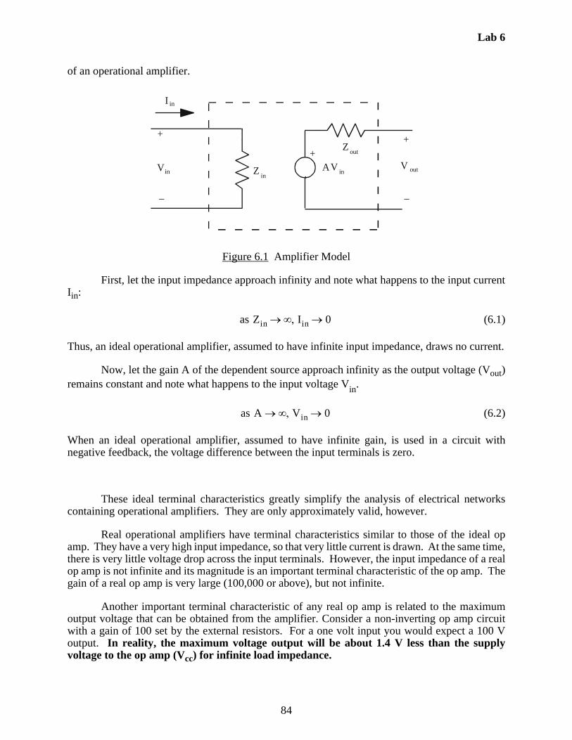
Lab 6
84
of an operational amplifier.
Figure 6.1 Amplifier Model
First, let the input impedance approach infinity and note what happens to the input currentIin:
as (6.1)
Thus, an ideal operational amplifier, assumed to have infinite input impedance, draws no current.
Now, let the gain A of the dependent source approach infinity as the output voltage (Vout)remains constant and note what happens to the input voltage Vin.
as (6.2)
When an ideal operational amplifier, assumed to have infinite gain, is used in a circuit withnegative feedback, the voltage difference between the input terminals is zero.
These ideal terminal characteristics greatly simplify the analysis of electrical networkscontaining operational amplifiers. They are only approximately valid, however.
Real operational amplifiers have terminal characteristics similar to those of the ideal opamp. They have a very high input impedance, so that very little current is drawn. At the same time,there is very little voltage drop across the input terminals. However, the input impedance of a realop amp is not infinite and its magnitude is an important terminal characteristic of the op amp. Thegain of a real op amp is very large (100,000 or above), but not infinite.
Another important terminal characteristic of any real op amp is related to the maximumoutput voltage that can be obtained from the amplifier. Consider a non-inverting op amp circuitwith a gain of 100 set by the external resistors. For a one volt input you would expect a 100 Voutput. In reality, the maximum voltage output will be about 1.4 V less than the supplyvoltage to the op amp (Vcc) for infinite load impedance.
VinV out
++
–
+
–
Zin
Zout
AV in
I in
Zin Iin 0
A Vin 0
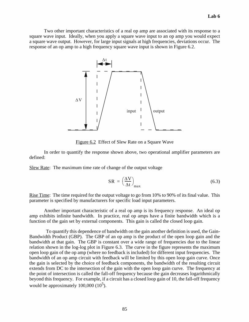
Lab 6
85
Two other important characteristics of a real op amp are associated with its response to asquare wave input. Ideally, when you apply a square wave input to an op amp you would expecta square wave output. However, for large input signals at high frequencies, deviations occur. Theresponse of an op amp to a high frequency square wave input is shown in Figure 6.2.
Figure 6.2 Effect of Slew Rate on a Square Wave
In order to quantify the response shown above, two operational amplifier parameters aredefined:
Slew Rate: The maximum time rate of change of the output voltage
(6.3)
Rise Time: The time required for the output voltage to go from 10% to 90% of its final value. Thisparameter is specified by manufacturers for specific load input parameters.
Another important characteristic of a real op amp is its frequency response. An ideal opamp exhibits infinite bandwidth. In practice, real op amps have a finite bandwidth which is afunction of the gain set by external components. This gain is called the closed loop gain.
To quantify this dependence of bandwidth on the gain another definition is used, the Gain-Bandwidth Product (GBP). The GBP of an op amp is the product of the open loop gain and thebandwidth at that gain. The GBP is constant over a wide range of frequencies due to the linearrelation shown in the log-log plot in Figure 6.3. The curve in the figure represents the maximumopen loop gain of the op amp (where no feedback is included) for different input frequencies. Thebandwidth of an op amp circuit with feedback will be limited by this open loop gain curve. Oncethe gain is selected by the choice of feedback components, the bandwidth of the resulting circuitextends from DC to the intersection of the gain with the open loop gain curve. The frequency atthe point of intersection is called the fall-off frequency because the gain decreases logarithmicallybeyond this frequency. For example, if a circuit has a closed loop gain of 10, the fall-off frequencywould be approximately 100,000 (105).
input output
V
t
SRVt--------
max=
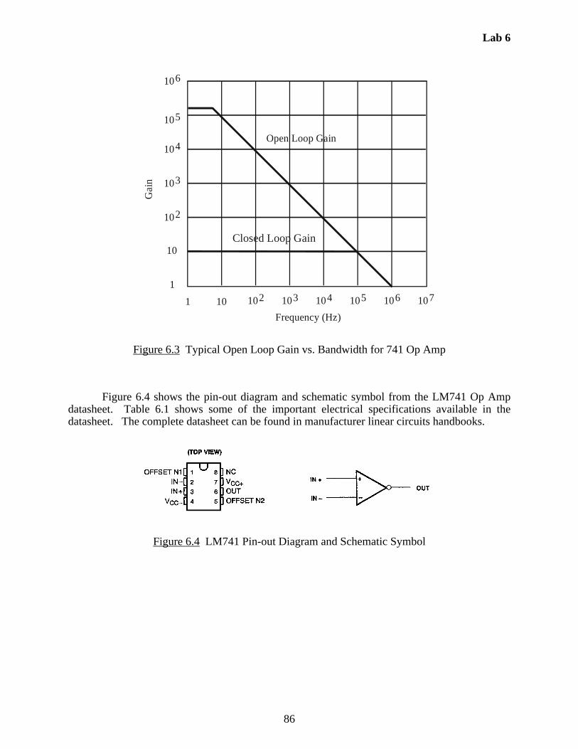
Lab 6
86
Figure 6.3 Typical Open Loop Gain vs. Bandwidth for 741 Op Amp
Figure 6.4 shows the pin-out diagram and schematic symbol from the LM741 Op Ampdatasheet. Table 6.1 shows some of the important electrical specifications available in thedatasheet. The complete datasheet can be found in manufacturer linear circuits handbooks.
Figure 6.4 LM741 Pin-out Diagram and Schematic Symbol
Frequency (Hz)
Gai
n
1 10 102 103 105 106 1071041
10
102
103
104
105
106
Open Loop Gain
Closed Loop Gain
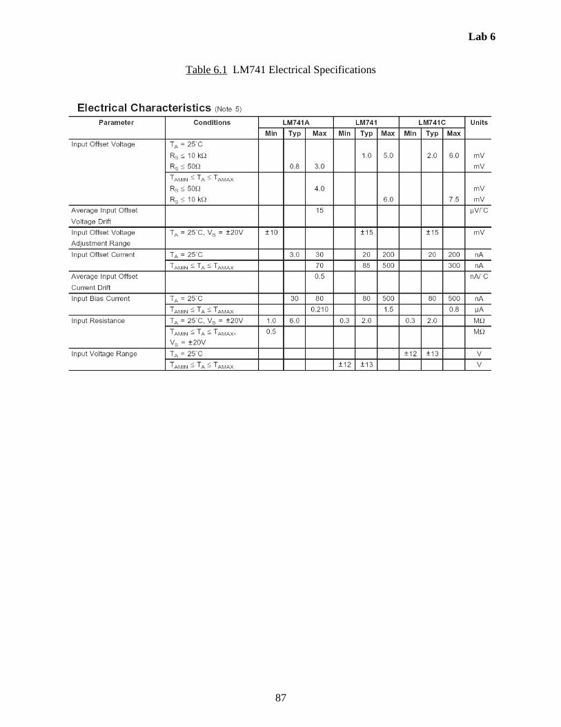
Lab 6
87
Table 6.1 LM741 Electrical Specifications

Lab 6
88

Lab 6
89
6.2 Laboratory Procedure / Summary Sheet
Group: ____ Names: _________________________ _____________________________
_________________________ _____________________________
An op amp requires connection to two different voltage levels from an external powersupply, usually +15V and -15V, both of which can be provided by a triple-output power supply.
NOTE - Before connecting +15V and -15V supplies to an op amp circuit, be verycareful to first set each voltage level on the power supply separately. To do thisusing older power supplies like the HP 6235A, first press the +18 button and turn the+/-18 VOLTAGE knob to adjust both voltages together. Then press the -18 buttonand turn the TRACK VOLTAGE knob to adjust the -18 voltage relative to the +18value. Also, make sure you know where the voltages should be attached beforemaking any connections. Also check both carefully and readjust if necessarybefore attaching. If the voltages are set too high by mistake, or if they areconnected improperly, you can easily damage the op amp.
(1) We will examine the usefulness of the high input impedance of the op amp byconstructing the simple circuit known as the voltage follower. Begin by building thecircuit shown in Figure 6.5a consisting of a voltage divider (R1, R2) and a loadresistance (R3) where R1=R2=R3=10k. Use Vin=5Vdc. Calculate the expectedvalue for Vout, with and without the load resistance in the circuit:
Then insert the op amp follower between the voltage divider and the load resistor asshown in Figure 6.5b. Be sure the op amp has the proper power supply connectionsas well as the signal connections shown in the figure. Again calculate the expectedvalue for Vout, with and without the load resistance in the circuit
Explain the differences among the voltages measured in the two circuits.
voltage calculated measured
Vout (w/o R3)
Vout (w/ R3)
voltage calculated measured
Vout (w/o R3)
Vout (w/ R3)
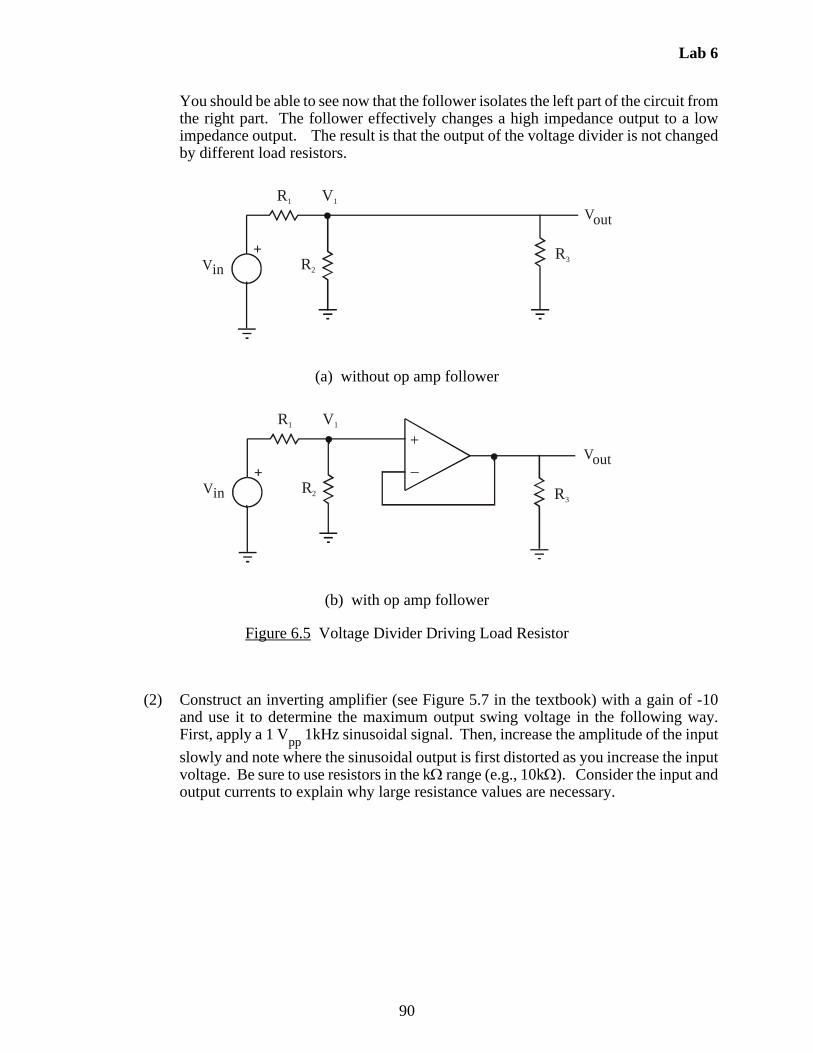
Lab 6
90
You should be able to see now that the follower isolates the left part of the circuit fromthe right part. The follower effectively changes a high impedance output to a lowimpedance output. The result is that the output of the voltage divider is not changedby different load resistors.
(a) without op amp follower
(b) with op amp follower
Figure 6.5 Voltage Divider Driving Load Resistor
(2) Construct an inverting amplifier (see Figure 5.7 in the textbook) with a gain of -10and use it to determine the maximum output swing voltage in the following way.First, apply a 1 Vpp 1kHz sinusoidal signal. Then, increase the amplitude of the input
slowly and note where the sinusoidal output is first distorted as you increase the inputvoltage. Be sure to use resistors in the k range (e.g., 10k). Consider the input andoutput currents to explain why large resistance values are necessary.
+Vin
Vout
R1
R3R2
V1
–
+
+Vin
Vout
R1
R3R2
V1
Lab 6
91
(3) Construct the modified integrator shown below. Normally, the shunt resistor (Rs) is
selected such that Rs 10 R1. Also, the product R1C is chosen to be approximately
equal to the period of the applied input voltage signal. Apply a 1 KHz, 1 Vp-p squarewave. Use the following component values: C = 0.1 F, Rs = 100 k, and R1 = R2
= 10 k. Justify these selections.
Figure 6.6 Integrator
Vin
V out
–
+
C
+
R s
R1
R 2
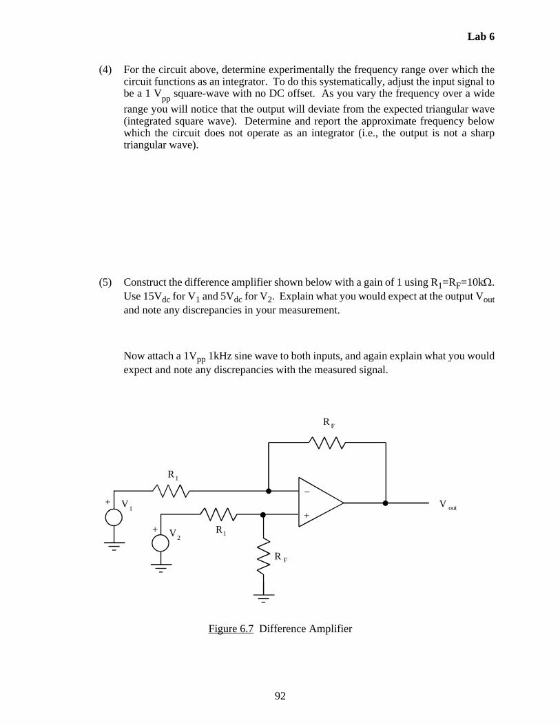
Lab 6
92
(4) For the circuit above, determine experimentally the frequency range over which thecircuit functions as an integrator. To do this systematically, adjust the input signal tobe a 1 Vpp square-wave with no DC offset. As you vary the frequency over a wide
range you will notice that the output will deviate from the expected triangular wave(integrated square wave). Determine and report the approximate frequency belowwhich the circuit does not operate as an integrator (i.e., the output is not a sharptriangular wave).
(5) Construct the difference amplifier shown below with a gain of 1 using R1=RF=10k.Use 15Vdc for V1 and 5Vdc for V2. Explain what you would expect at the output Voutand note any discrepancies in your measurement.
Now attach a 1Vpp 1kHz sine wave to both inputs, and again explain what you wouldexpect and note any discrepancies with the measured signal.
Figure 6.7 Difference Amplifier
R F
V out
–
+V1
+
+
R1
R F
R1V2

Lab 6
93
LAB 6 QUESTIONS
Group: ____ Names: _________________________ _____________________________
_________________________ _____________________________
(1) Find the specifications for the 741C op amp in the TI (uA741C) and/or NationalSemiconductor (LM741C) Linear Data Book and/or online. Record the values for each ofthe characteristic parameters listed below. Also, discuss the significance of eachparameter.
• input impedance
• output impedance
• maximum gain
• output voltage swing
• short circuit output current
(2) Explain how the voltage follower "isolates" the input from the output, and explain why thismight be useful.
(3) What is the fall-off frequency (approximate bandwidth) of a 741 op amp circuit designedwith a closed loop gain of 100?
(4) The output of the difference amp was not exactly zero when the inputs are of equalmagnitudes. Suggest possible causes for this discrepancy.

Lab 6
94
Lab 7
95
Laboratory 7
Digital Circuits - Logic and Latching
Required Components:• 1 330 resistor• 4 1k resistor• 2 0.1F capacitor• 1 2N3904 small signal transistor• 1 LED• 1 7408 AND gate IC• 1 7474 positive edge triggered flip-flop IC• 1 7475 data latch IC• 3 NO buttons
7.1 Objectives
In this laboratory exercise you will use TTL (transistor-to-transistor logic) integratedcircuits (ICs) to perform combinational and sequential logic functions. Specifically, you will learnhow to use logic gates and flip-flops. You will use these components to build a simple circuit tocontrol the display of an LED based on the past and current state of various switches or buttons.
7.2 Introduction
The ICs you will be handling in this laboratory exercise require digital inputs and producedigital outputs. A binary digital signal is a sequence of discrete states, in contrast to an analogsignal that varies continuously. Figure 7.1 shows the difference between digital and analog signals.The sampled digital data is a discrete representation of the analog signal. The data is representedby a series of bits.
Figure 7.1 Analog and Digital Signals
analog signal digitized signal
voltage
time
digitized point
sampled point
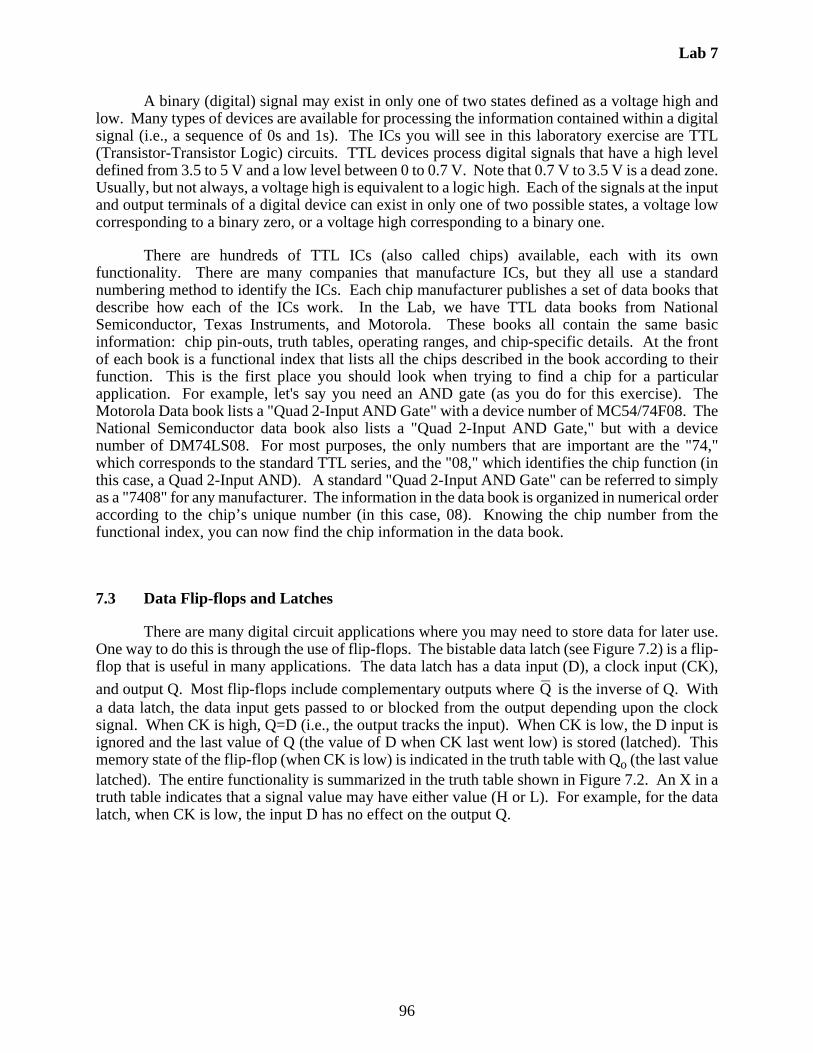
Lab 7
96
A binary (digital) signal may exist in only one of two states defined as a voltage high andlow. Many types of devices are available for processing the information contained within a digitalsignal (i.e., a sequence of 0s and 1s). The ICs you will see in this laboratory exercise are TTL(Transistor-Transistor Logic) circuits. TTL devices process digital signals that have a high leveldefined from 3.5 to 5 V and a low level between 0 to 0.7 V. Note that 0.7 V to 3.5 V is a dead zone.Usually, but not always, a voltage high is equivalent to a logic high. Each of the signals at the inputand output terminals of a digital device can exist in only one of two possible states, a voltage lowcorresponding to a binary zero, or a voltage high corresponding to a binary one.
There are hundreds of TTL ICs (also called chips) available, each with its ownfunctionality. There are many companies that manufacture ICs, but they all use a standardnumbering method to identify the ICs. Each chip manufacturer publishes a set of data books thatdescribe how each of the ICs work. In the Lab, we have TTL data books from NationalSemiconductor, Texas Instruments, and Motorola. These books all contain the same basicinformation: chip pin-outs, truth tables, operating ranges, and chip-specific details. At the frontof each book is a functional index that lists all the chips described in the book according to theirfunction. This is the first place you should look when trying to find a chip for a particularapplication. For example, let's say you need an AND gate (as you do for this exercise). TheMotorola Data book lists a "Quad 2-Input AND Gate" with a device number of MC54/74F08. TheNational Semiconductor data book also lists a "Quad 2-Input AND Gate," but with a devicenumber of DM74LS08. For most purposes, the only numbers that are important are the "74,"which corresponds to the standard TTL series, and the "08," which identifies the chip function (inthis case, a Quad 2-Input AND). A standard "Quad 2-Input AND Gate" can be referred to simplyas a "7408" for any manufacturer. The information in the data book is organized in numerical orderaccording to the chip’s unique number (in this case, 08). Knowing the chip number from thefunctional index, you can now find the chip information in the data book.
7.3 Data Flip-flops and Latches
There are many digital circuit applications where you may need to store data for later use.One way to do this is through the use of flip-flops. The bistable data latch (see Figure 7.2) is a flip-flop that is useful in many applications. The data latch has a data input (D), a clock input (CK),
and output Q. Most flip-flops include complementary outputs where is the inverse of Q. Witha data latch, the data input gets passed to or blocked from the output depending upon the clocksignal. When CK is high, Q=D (i.e., the output tracks the input). When CK is low, the D input isignored and the last value of Q (the value of D when CK last went low) is stored (latched). Thismemory state of the flip-flop (when CK is low) is indicated in the truth table with Qo (the last valuelatched). The entire functionality is summarized in the truth table shown in Figure 7.2. An X in atruth table indicates that a signal value may have either value (H or L). For example, for the datalatch, when CK is low, the input D has no effect on the output Q.
Q
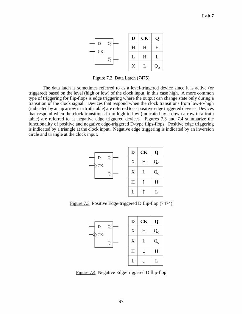
Lab 7
97
Figure 7.2 Data Latch (7475)
The data latch is sometimes referred to as a level-triggered device since it is active (ortriggered) based on the level (high or low) of the clock input, in this case high. A more commontype of triggering for flip-flops is edge triggering where the output can change state only during atransition of the clock signal. Devices that respond when the clock transitions from low-to-high(indicated by an up arrow in a truth table) are referred to as positive edge triggered devices. Devicesthat respond when the clock transitions from high-to-low (indicated by a down arrow in a truthtable) are referred to as negative edge triggered devices. Figures 7.3 and 7.4 summarize thefunctionality of positive and negative edge-triggered D-type flips-flops. Positive edge triggeringis indicated by a triangle at the clock input. Negative edge triggering is indicated by an inversioncircle and triangle at the clock input.
Figure 7.3 Positive Edge-triggered D flip-flop (7474)
Figure 7.4 Negative Edge-triggered D flip-flop
D CK Q
H H H
L H L
X L Qo
D CK Q
X H Qo
X L Qo
H H
L L
D CK Q
X H Qo
X L Qo
H H
L L
D Q
Q
CK
D Q
Q
CK
D Q
Q
CK
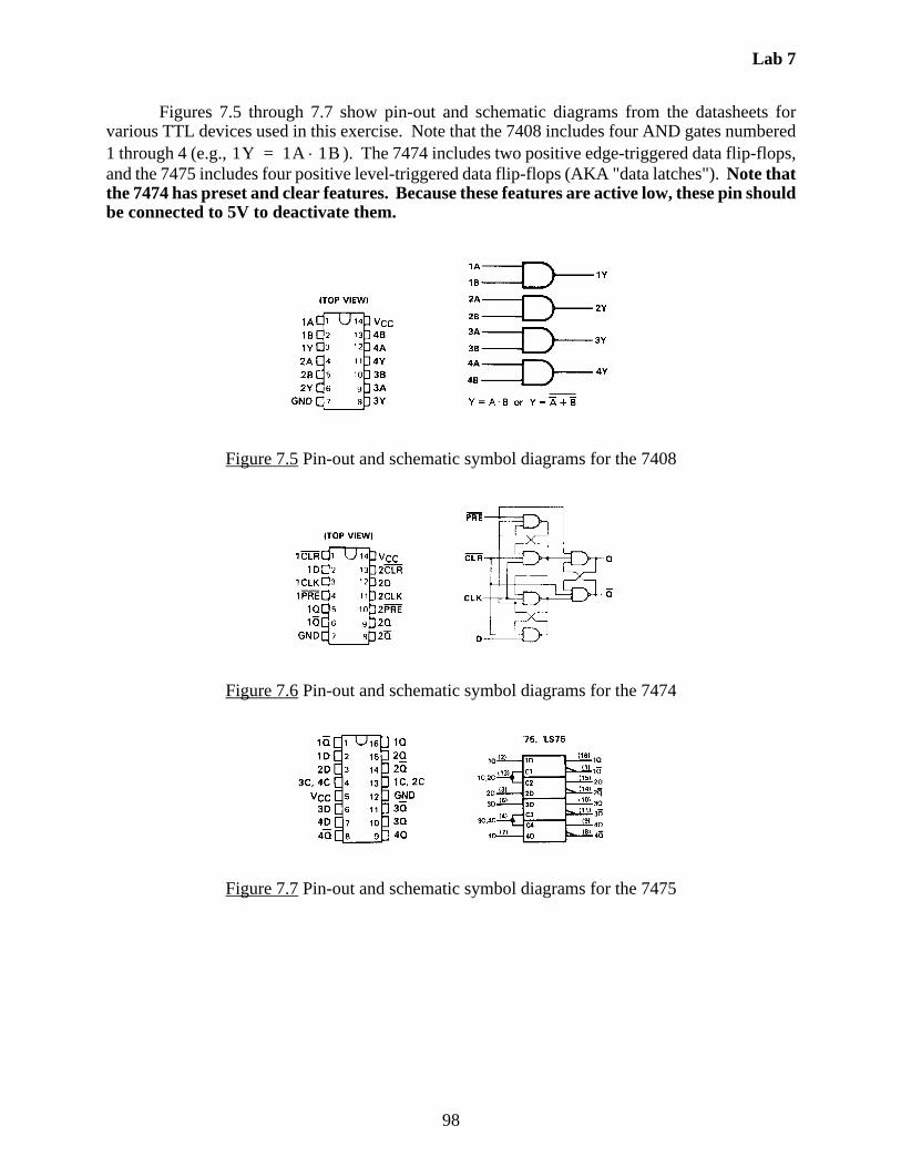
Lab 7
98
Figures 7.5 through 7.7 show pin-out and schematic diagrams from the datasheets forvarious TTL devices used in this exercise. Note that the 7408 includes four AND gates numbered1 through 4 (e.g., ). The 7474 includes two positive edge-triggered data flip-flops,and the 7475 includes four positive level-triggered data flip-flops (AKA "data latches"). Note thatthe 7474 has preset and clear features. Because these features are active low, these pin shouldbe connected to 5V to deactivate them.
Figure 7.5 Pin-out and schematic symbol diagrams for the 7408
Figure 7.6 Pin-out and schematic symbol diagrams for the 7474
Figure 7.7 Pin-out and schematic symbol diagrams for the 7475
1Y 1A 1B=

Lab 7
99
7.4 Hints on assembling and troubleshooting breadboard circuits including integratedcircuits
Please follow the protocol listed below when using breadboards to construct and testprototype circuits containing integrated circuits (ICs). Generally, if you carefully follow thisprotocol you will avoid a lot of frustration
(1) Start with a clearly drawn schematic illustrating all components, inputs, outputs, andconnections.
(2) Draw a detailed wiring diagram, using the information from handbooks regardingdevice pin-outs. Label and number each pin used on each IC and fully specify eachcomponent. This will be your wiring guide.
(3) Double check the functions you want to perform with each device.
(4) Insert the ICs into your breadboard, and select appropriately colored wire (i.e. red for+5V, black for ground, other colors for signals).
(5) Wire up all connections, overwriting the wiring diagram with a red pen or highlighteras you insert each wire. Use appropriate lengths (~ 1/4") for exposed wire ends. Ifthe ends are too short, you might not establish good connections; and if too long, youmight damage the breadboard. Also be careful to not insert component (e.g., resistorand capacitor) leads too far into the breadboard holes. This can also result inbreadboard damage.
(6) Double check the +5V and ground connections to each IC.
(7) Set the power supply to +5V and turn it off.
(8) Connect the power supply to your breadboard and then turn it on.
(9) Measure signals at inputs and outputs to verify proper functionality.
(10) If your circuit is not functioning properly, go back through the above steps in reverseorder checking everything carefully. If you are still having difficulty, use the beepcontinuity-check feature on the multimeter to verify all connections.
(11) When removing ICs from the breadboard, use a chip-puller tool to limit the potentialfor pin damage.
(12) See more useful information and guidance in Lab 15.
And for additional troubleshooting advice, especially formore-complicated circuits and the Project, see Section 2.3 inLab 2 and Section 15.5 in Lab 15.

Lab 7
100
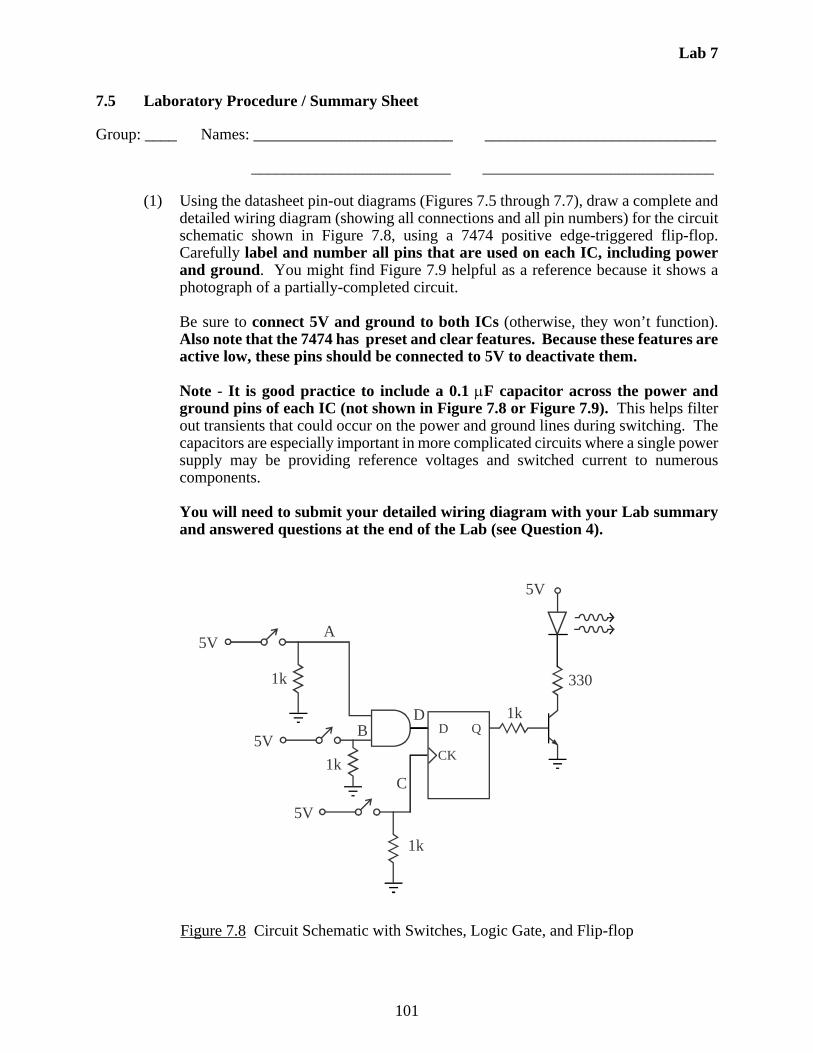
Lab 7
101
7.5 Laboratory Procedure / Summary Sheet
Group: ____ Names: _________________________ _____________________________
_________________________ _____________________________
(1) Using the datasheet pin-out diagrams (Figures 7.5 through 7.7), draw a complete anddetailed wiring diagram (showing all connections and all pin numbers) for the circuitschematic shown in Figure 7.8, using a 7474 positive edge-triggered flip-flop.Carefully label and number all pins that are used on each IC, including powerand ground. You might find Figure 7.9 helpful as a reference because it shows aphotograph of a partially-completed circuit.
Be sure to connect 5V and ground to both ICs (otherwise, they won’t function).Also note that the 7474 has preset and clear features. Because these features areactive low, these pins should be connected to 5V to deactivate them.
Note - It is good practice to include a 0.1 F capacitor across the power andground pins of each IC (not shown in Figure 7.8 or Figure 7.9). This helps filterout transients that could occur on the power and ground lines during switching. Thecapacitors are especially important in more complicated circuits where a single powersupply may be providing reference voltages and switched current to numerouscomponents.
You will need to submit your detailed wiring diagram with your Lab summaryand answered questions at the end of the Lab (see Question 4).
Figure 7.8 Circuit Schematic with Switches, Logic Gate, and Flip-flop
D Q
CK
330
5V
1k
5V
1k
5V
C
1k
5VA
B1kD
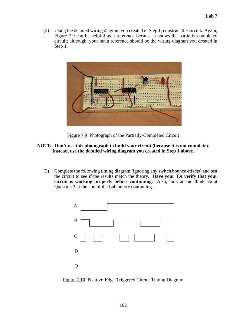
Lab 7
102
(2) Using the detailed wiring diagram you created in Step 1, construct the circuit. Again,Figure 7.9 can be helpful as a reference because it shows the partially completedcircuit; although, your main reference should be the wiring diagram you created inStep 1.
Figure 7.9 Photograph of the Partially-Completed Circuit
NOTE - Don’t use this photograph to build your circuit (because it is not complete).Instead, use the detailed wiring diagram you created in Step 1 above.
(3) Complete the following timing diagram (ignoring any switch bounce effects) and testthe circuit to see if the results match the theory. Have your TA verify that yourcircuit is working properly before continuing. Also, look at and think aboutQuestion 2 at the end of the Lab before continuing.
Figure 7.10 Positive-Edge-Triggered Circuit Timing Diagram
A
B
C
D
Q
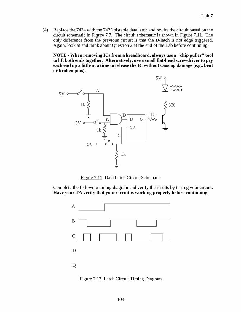
Lab 7
103
(4) Replace the 7474 with the 7475 bistable data latch and rewire the circuit based on thecircuit schematic in Figure 7.7. The circuit schematic is shown in Figure 7.11. Theonly difference from the previous circuit is that the D-latch is not edge triggered.Again, look at and think about Question 2 at the end of the Lab before continuing.
NOTE - When removing ICs from a breadboard, always use a "chip puller" toolto lift both ends together. Alternatively, use a small flat-head screwdriver to pryeach end up a little at a time to release the IC without causing damage (e.g., bentor broken pins).
Figure 7.11 Data Latch Circuit Schematic
Complete the following timing diagram and verify the results by testing your circuit.Have your TA verify that your circuit is working properly before continuing.
Figure 7.12 Latch Circuit Timing Diagram
D Q
CK
330
5V
1k
5V
1k
5V
C
1k
5VA
B1kD
A
B
C
D
Q

Lab 7
104
LAB 7 QUESTIONS
Group: ____ Names: _________________________ _____________________________
_________________________ _____________________________
(1) Explain the difference between the output of the two circuits you analyzed and tested.What is the reason for the difference?
(2) Switches and buttons often experience switch "bounce," especially when contact is made(as opposed to broken). Did bounce affect the output Q of the circuits? If so, in what cases,and why? If not, explain why you think this was the case.
For the positive-edge-triggered circuit (Figure 7.8), assuming bounce occurs during everyrelease of button C, draw a timing diagram showing how the output (Q) would respond forthe A, B, and C traces shown in Figure 7.10.

Lab 7
105
For the timing diagram inputs shown in Figures 7.10 and 7.12, would you expect to noticeany changes in the LED response if there were switch bounce during both the presses andreleases of switches A and B (but not C)? Why or why not?
(3) What is the purpose for the resistors between the switch outputs and ground?
(4) Attach the detailed wiring diagram you used to construct the 7474 circuit. Make sure all ofthe pins used are labeled and numbered.

Lab 7
106

Lab 8
107
Laboratory 8
Digital Circuits - Counter and LED Display
Required Components:• 2 1k resistors• 1 10M resistor• 3 0.1F capacitor• 1 555 timer • 1 7490 decade counter• 1 7447 BCD to LED decoder• 1 MAN 6910 or LTD-482EC seven-segment LED digital display• 1 330 DIP resistor array• 2 NO buttons
8.1 Objectives
In this laboratory exercise you will build a digital counter with a 1-digit decimal LEDdisplay. In doing so, you will learn to assemble and interconnect various integrated circuits toachieve sophisticated functionality.
8.2 Introduction
A common requirement in digital circuits applications is to count and display the numberof pulses contained in a continuous TTL compatible pulse train (e.g., the output of a proximitysensor detecting parts on a moving conveyor belt or a photosensor detecting a reflection from apiece of tape on a rotating shaft). We want to count the number of pulses and output this numberin binary coded form. This can be done using a 7490 decade counter. Refer to the 7490 pin-outand function information in Figure 8.1.
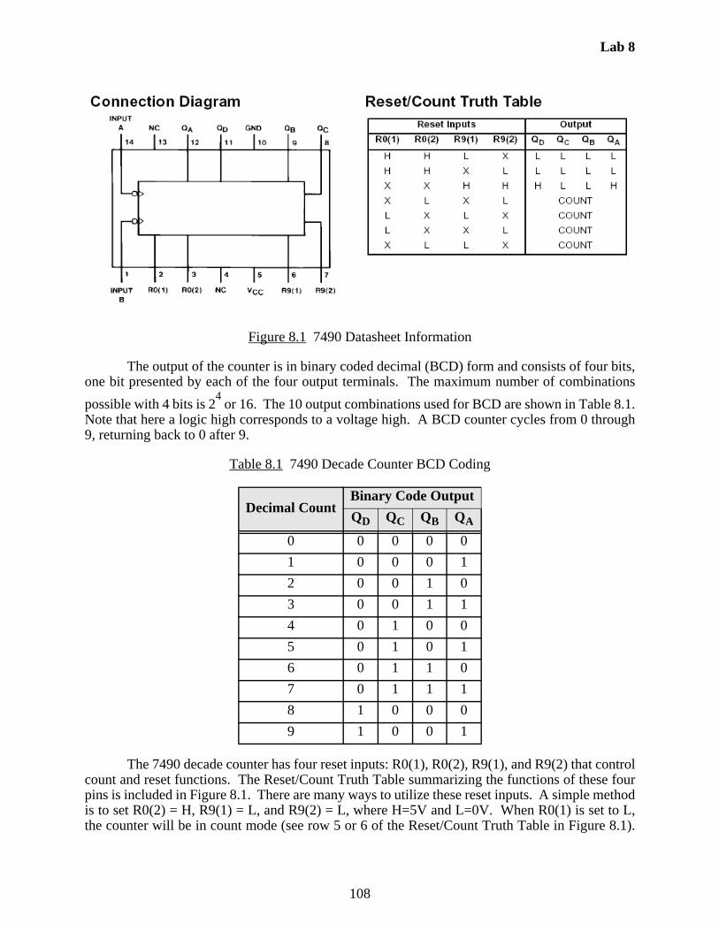
Lab 8
108
Figure 8.1 7490 Datasheet Information
The output of the counter is in binary coded decimal (BCD) form and consists of four bits,one bit presented by each of the four output terminals. The maximum number of combinations
possible with 4 bits is 24 or 16. The 10 output combinations used for BCD are shown in Table 8.1.
Note that here a logic high corresponds to a voltage high. A BCD counter cycles from 0 through9, returning back to 0 after 9.
Table 8.1 7490 Decade Counter BCD Coding
The 7490 decade counter has four reset inputs: R0(1), R0(2), R9(1), and R9(2) that controlcount and reset functions. The Reset/Count Truth Table summarizing the functions of these fourpins is included in Figure 8.1. There are many ways to utilize these reset inputs. A simple methodis to set R0(2) = H, R9(1) = L, and R9(2) = L, where H=5V and L=0V. When R0(1) is set to L,the counter will be in count mode (see row 5 or 6 of the Reset/Count Truth Table in Figure 8.1).
Decimal CountBinary Code Output
QD QC QB QA
0 0 0 0 0
1 0 0 0 1
2 0 0 1 0
3 0 0 1 1
4 0 1 0 0
5 0 1 0 1
6 0 1 1 0
7 0 1 1 1
8 1 0 0 0
9 1 0 0 1

Lab 8
109
When R0(1) is set to H, the counter will reset to 0 (LLLL) (see rows 1 and 2 of the Reset/CountTruth Table).
It is also convenient to display the output count on a 7 segment LED in digit form. Anotherdevice will be necessary to decode the four bits into a form compatible with the LED array. Thisdevice, the 7447 BCD-to-seven-segment decoder, converts the BCD binary number at its inputsinto a 7 segment code to properly drive the LED digit (see Figure 8.2). The function tabledescribing the input (BCD) to output (7-segment LED code) relationship for the 7447 is shown inTable 8.2. Refer to Figure 8.3 for the pin-out diagram for the device.
Figure 8.2 Seven-Segment LED Display (LCD)
Table 8.2 7447 BCD to 7-segment Decoder
DecimalDigit
Input Output
QD QC QB QA a b c d e f g
0 0 0 0 0 0 0 0 0 0 0 1
1 0 0 0 1 1 0 0 1 1 1 1
2 0 0 1 0 0 0 1 0 0 1 0
3 0 0 1 1 0 0 0 0 1 1 0
4 0 1 0 0 1 0 0 1 1 0 0
5 0 1 0 1 0 1 0 0 1 0 0
6 0 1 1 0 1 1 0 0 0 0 0
7 0 1 1 1 0 0 0 1 1 1 1
8 1 0 0 0 0 0 0 0 0 0 0
9 1 0 0 1 0 0 0 1 1 0 0
a
b
c
d
e
f
g
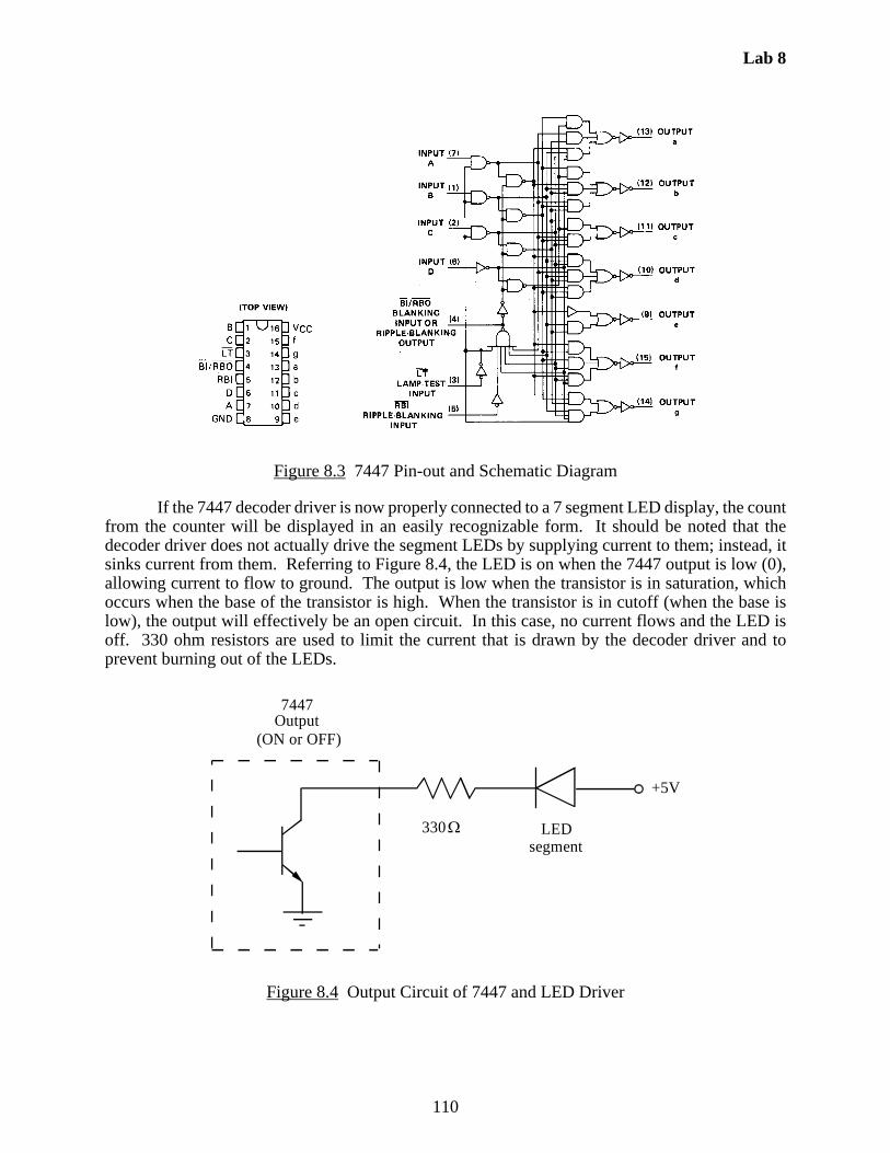
Lab 8
110
Figure 8.3 7447 Pin-out and Schematic Diagram
If the 7447 decoder driver is now properly connected to a 7 segment LED display, the countfrom the counter will be displayed in an easily recognizable form. It should be noted that thedecoder driver does not actually drive the segment LEDs by supplying current to them; instead, itsinks current from them. Referring to Figure 8.4, the LED is on when the 7447 output is low (0),allowing current to flow to ground. The output is low when the transistor is in saturation, whichoccurs when the base of the transistor is high. When the transistor is in cutoff (when the base islow), the output will effectively be an open circuit. In this case, no current flows and the LED isoff. 330 ohm resistors are used to limit the current that is drawn by the decoder driver and toprevent burning out of the LEDs.
Figure 8.4 Output Circuit of 7447 and LED Driver
7447 Output
(ON or OFF)
LED segment
330
+5V
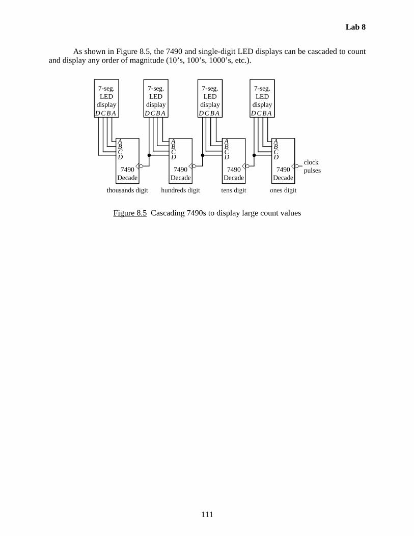
Lab 8
111
As shown in Figure 8.5, the 7490 and single-digit LED displays can be cascaded to countand display any order of magnitude (10’s, 100’s, 1000’s, etc.).
Figure 8.5 Cascading 7490s to display large count values
thousands digit hundreds digit tens digit ones digit
7490 Decade
CD
BA
7490 Decade
CD
BA
7490 Decade
CD
BA
7490 Decade
CD
BA
clock pulses
7-seg. LED
displayD B AC
7-seg. LED
displayD B AC
7-seg. LED
displayD BAC
7-seg. LED
displayD BAC
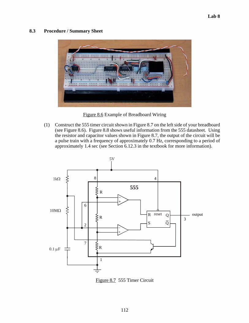
Lab 8
112
8.3 Procedure / Summary Sheet
Figure 8.6 Example of Breadboard Wiring
(1) Construct the 555 timer circuit shown in Figure 8.7 on the left side of your breadboard(see Figure 8.6). Figure 8.8 shows useful information from the 555 datasheet. Usingthe resistor and capacitor values shown in Figure 8.7, the output of the circuit will bea pulse train with a frequency of approximately 0.7 Hz, corresponding to a period ofapproximately 1.4 sec (see Section 6.12.3 in the textbook for more information).
Figure 8.7 555 Timer Circuit
outputR
S
R
R
R
Q
–+
–+
1
2
3
4
6
7
8
Q
555
reset
5V
1k
10M
0.1 F
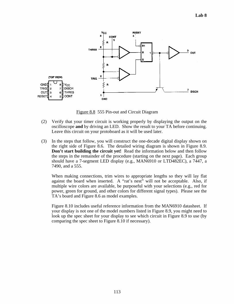
Lab 8
113
Figure 8.8 555 Pin-out and Circuit Diagram
(2) Verify that your timer circuit is working properly by displaying the output on theoscilloscope and by driving an LED. Show the result to your TA before continuing.Leave this circuit on your protoboard as it will be used later.
(3) In the steps that follow, you will construct the one-decade digital display shown onthe right side of Figure 8.6. The detailed wiring diagram is shown in Figure 8.9.Don’t start building the circuit yet! Read the information below and then followthe steps in the remainder of the procedure (starting on the next page). Each groupshould have a 7-segment LED display (e.g., MAN6910 or LTD482EC), a 7447, a7490, and a 555.
When making connections, trim wires to appropriate lengths so they will lay flatagainst the board when inserted. A “rat’s nest” will not be acceptable. Also, ifmultiple wire colors are available, be purposeful with your selections (e.g., red forpower, green for ground, and other colors for different signal types). Please see theTA’s board and Figure 8.6 as model examples.
Figure 8.10 includes useful reference information from the MAN6910 datasheet. Ifyour display is not one of the model numbers listed in Figure 8.9, you might need tolook up the spec sheet for your display to see which circuit in Figure 8.9 to use (bycomparing the spec sheet to Figure 8.10 if necessary).
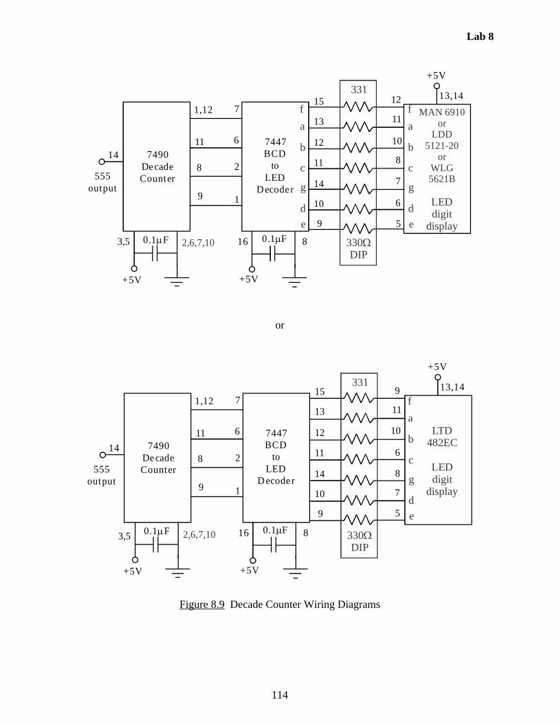
Lab 8
114
or
Figure 8.9 Decade Counter Wiring Diagrams
+5V
+5V+5V
13,1412
11
10
8
7
6
5
15
13
12
11
14
10
9
7
6
2
1
1,12
11
8
9
816
7447 BCD
to LED
Decoder
7490 Decade Counter
3,5 0.1F0.1F
f
a
b
c
g
d
e
f
a
b
c
g
d
e
MAN 6910or
LDD5121-20
orWLG5621B
LEDdigit
display
330DIP
331
555 output
14
2,6,7,10
555 output
9
11
10
6
8
7
5
+5V
+5V+5V
13,147
6
2
1
1,12
11
8
9
816
14
7447 BCD
to LED
Decoder
7490 Decade Counter
0.1F0.1F
f
a
b
c
g
d
e
LTD482EC
LEDdigit
display
330DIP
331
2,6,7,103,5
15
13
12
11
14
10
9
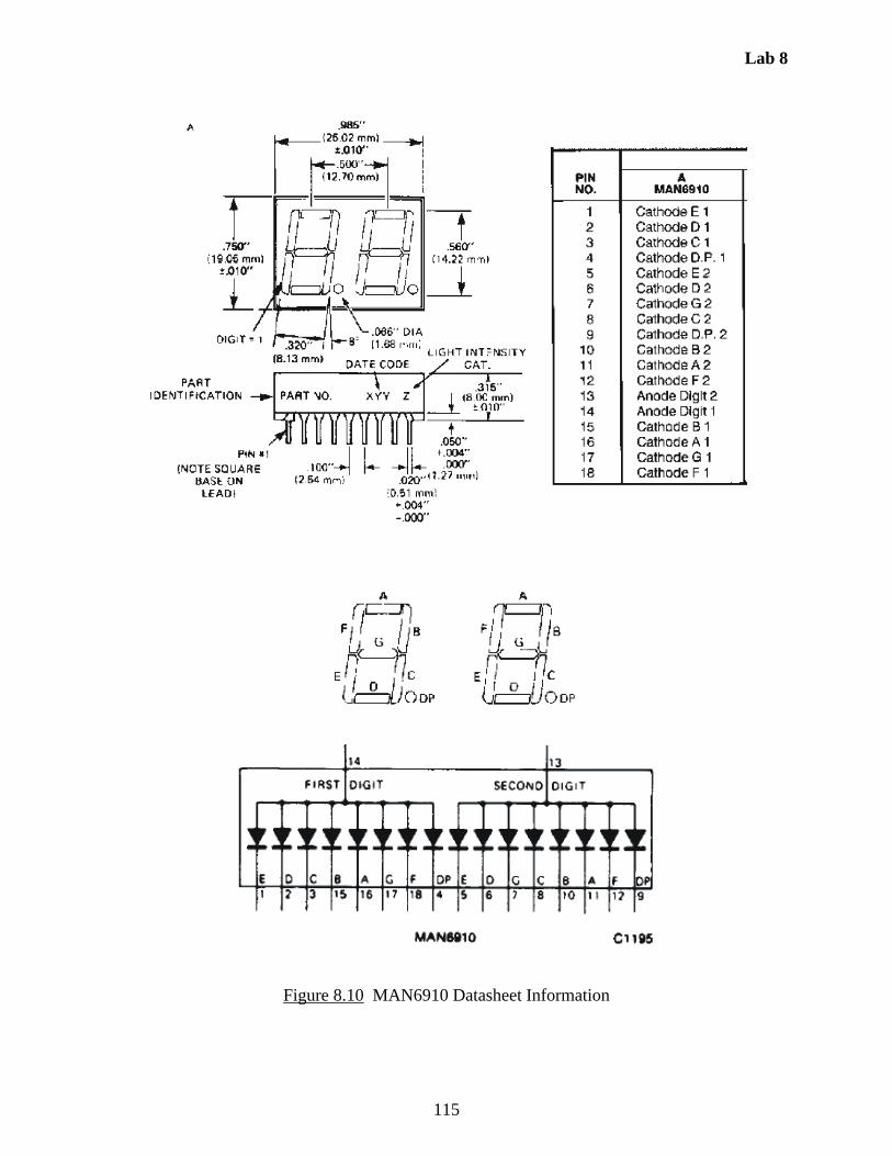
Lab 8
115
Figure 8.10 MAN6910 Datasheet Information

Lab 8
116
(4) Wire the top and bottom two rows of the breadboard together as shown in Figure 8.6so both power (+5V) and ground will be accessible on both sides of the board. Thismakes it convenient to connect to +5V and ground on either side of a component. Itis good practice to leave the power supply off and disconnected while working on thecircuits. Only when you are ready for a test should you turn on the power supply,check to make sure the voltage is set to +5V, and then connect to your board.
(5) Before inserting any components in the board, be sure to lay them all out first to makesure everything will fit. Figure 8.6 shows a suggested board layout.
(6) Insert the MAN6910 2-digit display on the right side of the board, with the cornerlabeled MAN6910 at the lower-left side. This label marks pin 1 on the MAN6910.
(7) Insert the 330 DIP resistor IC next to the display. Connect pins 13 and 14 of theMAN6910 to +5 V (see Figure 8.10 for MAN6910 pin-out information). Nothingmore for now! As a test, connect three of the 330 DIP resistors to pins 3, 15, and16 of the MAN6910, grounding the other ends of the resistors. Double-check yourcircuit, and then turn on and connect the power supply. Is the displayed digit whatyou expected? If not, consult with your TA. When you are done with this test, turnoff and disconnect the power supply until you are ready for the next test. Also removeall of the resistor connections.
(8) Insert the 7447 IC next to the 330 DIP resistor IC. Per Figure 8.9, connect theMAN6910 one's (right) digit to the 7447 and connect +5V and ground as shown.
(9) Activate the 7447 lamp test by attaching 0V to pin 3 and 5 V to pin 4. Turn on andattach the power supply to see if all LED segments come on, as they should.
(10) Remove the wire from pin 3 and apply +5V to pins 1, 2, 7 and ground to pin 6 of the7447. Does the display show what you think it should? Turn off and disconnect thepower supply before continuing.
(11) Finish wiring the 7447 and 7490 as shown in Figure 8.9. Refer to the 7490 Reset/Count Truth Table and the description of the reset inputs in Section 8.2. In Figure 8.9,pins 2, 6 and 7 (R0(1), R9(1) and R9(2)) are grounded and pin 3 (R0(2)) is held high,putting the 7490 in count mode. To be able to reset the counter, wire up a normally-open (NO) button to pin 2 (R0(1)) so the signal is low when the button is not pressed(see Question 2 below). When R0(1)=L, the counter will be in count mode, and whenR0(1)=H (when the button is pressed), the counter will reset to 0.
(12) Attach the output of your 555 to the input of the 7490. Double-check your entirecircuit! Then turn on and attach the power supply to see if your circuit is workingproperly. If not, see Section 7.4 in the previous Lab for debugging advice.
(13) Demonstrate to the TA that your display can increment properly from 0 to 9. At thesame time, also demonstrate that you can reset the counter to 0.
(14) Now disconnect the 555 circuit and wire up a button with a pull-up resistor to the7490 input instead. Press the button a few times and describe what happens and whyin Question 3 below.

Lab 8
117
8.4 Troubleshooting Advice
Often, when assembling complicated circuits like those in this Lab and in your Project,things rarely work the first time because you will often make mistakes. Also, sometimes yourconnections won’t be reliable. When this happens, try to remain calm and logically "debug" ortroubleshoot the problem.
Any time you have any problem with any circuit, especially with your Project, carefullyfollow all of the troubleshooting advice outlines in Section 2.3 in Lab 2, Section 7.4 in Lab 7, andSection 15.5 in Lab 15.

Lab 8
118

Lab 8
119
LAB 8 QUESTIONS
Group: ____ Names: _________________________ _____________________________
_________________________ _____________________________
(1) Which pins of the 7447 should be high to display a "b"?
(2) Draw a schematic of the circuit you used to wire up the normally open (NO) button to resetthe counter to 0. Show all required added components and wiring.
(3) When the button is used for the input instead of the 555 circuit, what did you observe witheach press and release of the button, and why? Be specific.

Lab 8
120
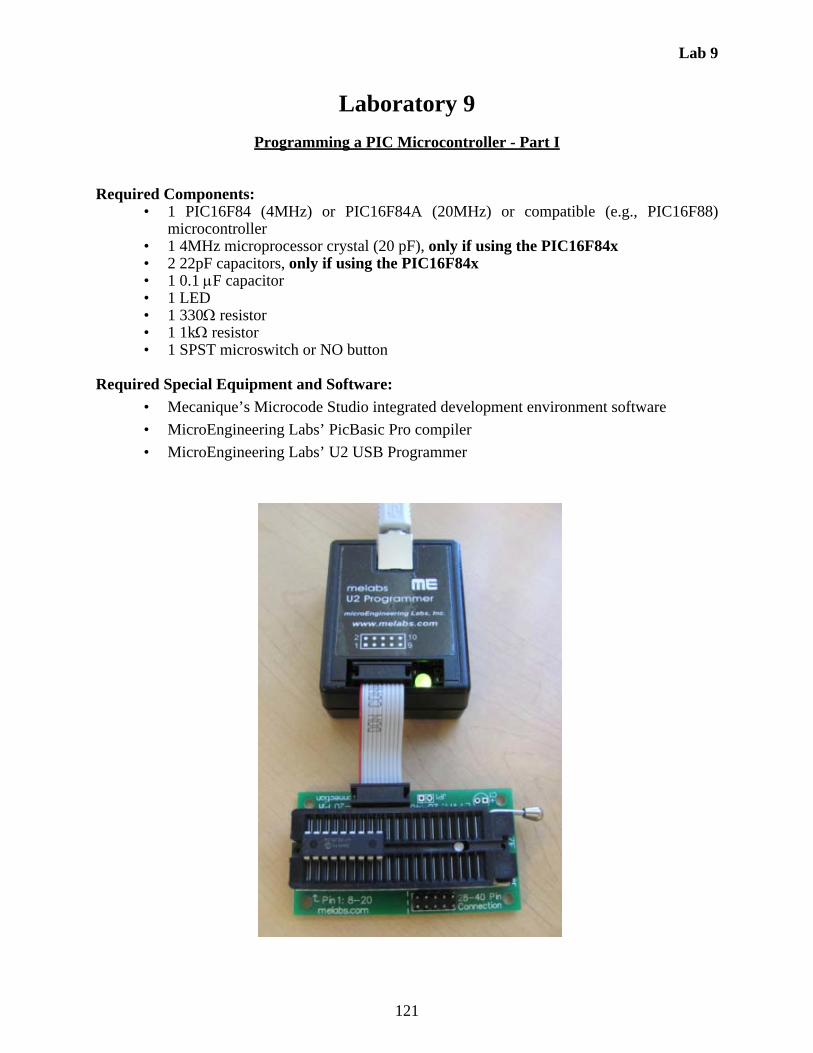
Lab 9
121
Laboratory 9
Programming a PIC Microcontroller - Part I
Required Components:• 1 PIC16F84 (4MHz) or PIC16F84A (20MHz) or compatible (e.g., PIC16F88)
microcontroller• 1 4MHz microprocessor crystal (20 pF), only if using the PIC16F84x• 2 22pF capacitors, only if using the PIC16F84x• 1 0.1 F capacitor• 1 LED• 1 330 resistor• 1 1k resistor• 1 SPST microswitch or NO button
Required Special Equipment and Software:
• Mecanique’s Microcode Studio integrated development environment software
• MicroEngineering Labs’ PicBasic Pro compiler
• MicroEngineering Labs’ U2 USB Programmer

Lab 9
122
9.1 Objective
Microcontrollers are important parts in the design and control of mechatronic systems.This laboratory introduces the architecture of Microchip’s PIC microcontroller, describes thePIC’s capabilities, shows how to create programs using microEngineering Lab’s PicBASIC Pro,and shows how to wire simple circuits using the PIC and your software. The exercise also showshow to use interrupts in response to sensor inputs to the PIC.
9.2 Introduction
A PIC microcontroller adds sophisticated digital control capabilities when connected toother circuits and devices. A single PIC microcontroller can communicate with other electronicdevices, and digitally switch them on or off to control simple operations.
Microchip Technology, Inc. (www.microchip.com) produces a family of PIC processorscapable of storing programs. The PIC16F84, which we will use in this Lab, contains electricallyerasable programmable ROM (EEPROM), which is memory used to store programs. The programin EEPROM can be overwritten many times during the design cycle. The PIC has 64 bytes of dataEEPROM and 1792 bytes of program EEPROM for storing compiled programs. It operates at 4or 8 MHz depending upon an external crystal oscillator or a timer circuit. The PIC16F84A canfunction up to 20 MHz. The 18-pin PIC has 13 pins capable of operating as either inputs or outputs,designated by software, that can be changed during program execution. Five of the pins aregrouped together and referenced as PORTA; another 8 pins are grouped together and referenced asPORTB.
Simple programs may be written in a form of BASIC called PicBasic Pro, which isavailable from microEngineering Labs, Inc. (www.melabs.com). The package includes a compilerthat converts PicBasic to assembly language code, and then compiles the assembly code tohexadecimal machine code (hex) that is downloaded to the PIC. The hex executable code isdownloaded via a serial port to a PIC using the Microchip Development Programmer hardwareusing a Windows interface. Once written, the program remains in PIC memory even when thepower is removed.
9.2.1 PIC Structure
The PIC16F84 is an 18-pin DIP IC with the pin-out shown in the top of Figure 9.1. It hasexternal power and ground pins (Vdd and Vss), 13 binary input/output (I/O) pins (RA[0-4] andRB[0-7]), and uses an external oscillator (the crystal and capacitor circuit attached to OSC1 and
OSC2) to generate a clock signal. The master clear ( ) pin is active low, meaning the PIC
is reset when the pin is grounded. must be held high during PIC operation, or be drivenlow on purpose (e.g., by a reset button) to reset the PIC and restart your program. There are manyPIC microcontrollers that are pin-compatible with the PIC16F84, including the PIC16F88 shownin the bottom of Figure 9.1. The PIC16F88, like most advanced PICs, provides alternativefunctions for the pins. Only some of the alternative functions are listed in Figure 9.1 (see thePIC16F88 datasheet online for more information). For example, the RA[0-4] pins can be used as
MCLR
MCLR
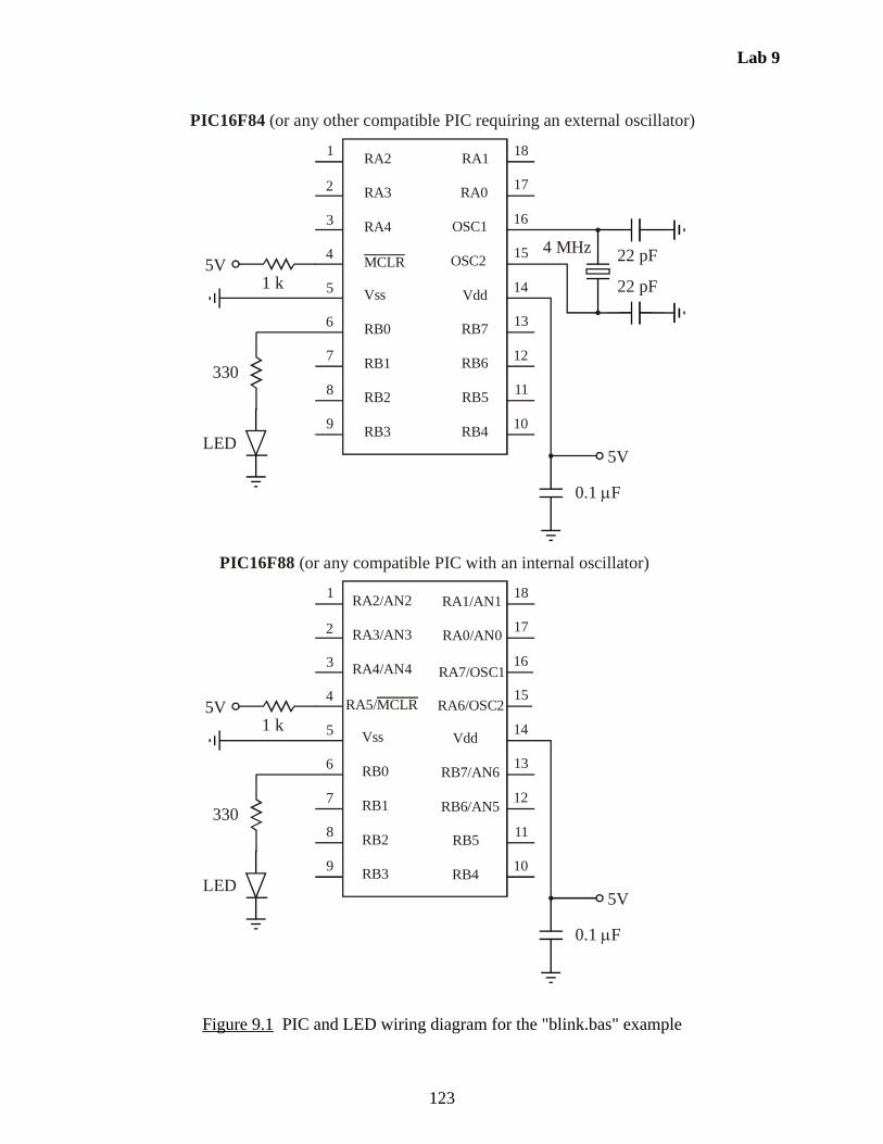
Lab 9
123
Figure 9.1 PIC and LED wiring diagram for the "blink.bas" example
PIC16F84 (or any other compatible PIC requiring an external oscillator)
RA2
RA3
RA4
MCLR
Vss
RB0
RB1
RB2
RB3
RA1
RA0
OSC1
OSC2
Vdd
RB7
RB6
RB5
RB4
1
2
3
4
5
6
7
8
9 10
11
12
13
14
15
16
17
18
5V22 pF
22 pF
4 MHz
1 k
5V
0.1 F
330
LED
PIC16F88 (or any compatible PIC with an internal oscillator)
RA2/AN2
RA3/AN3
RA4/AN4
RA5/MCLR
Vss
RB0
RB1
RB2
RB3
RA1/AN1
RA0/AN0
RA7/OSC1
RA6/OSC2
Vdd
RB7/AN6
RB6/AN5
RB5
RB4
1
2
3
4
5
6
7
8
9 10
11
12
13
14
15
16
17
18
5V1 k
5V
0.1 F
330
LED

Lab 9
124
analog inputs (AN[0-4]) instead, and the pin can be used as an additional I/O pin (RA5).Also, the PIC16F88, like many PICS, includes an internal oscillator, so it does not require anexternal clock circuit. Therefore, the OSC1/OSC2 pins can be used as additional I/O pins (RA6-7) instead (and the external crystals and capacitors are not required). Throughout all of the PICLabs, we will use the PIC16F88 (or some other PIC compatible with the PIC16F84), but it will beconfigured to look just like the PIC16F84 (except for the oscillator).
The power supply voltage (5 Vdc) and ground are connected to pins labeled Vdd and Vss
(pins 14 and 5), respectively. Pin 4 ( ) is attached to 5Vdc with a 1k resistor to ensurecontinuous operation. If this pin were left unconnected (floating), the PIC could spontaneouslyreset itself. With the PIC16F84, an accurate clock frequency can be obtained by connecting a4MHz crystal (sometimes indicated as XT) across pins 15 and 16 which are also connected toground through 22pF capacitors. A less expensive and less accurate alternative for setting a clockfrequency is to attach an RC circuit to pin 16 while leaving pin 15 unattached (referred to as an RCclock).
The pins labelled RAx and RBx provide binary I/O. They are divided into two groups calledPORTs. PORTA refers to pins RA0 through RA4 and PORTB refers to pins RB0 through RB7.PORTA and PORTB are compiler variable names that provide access to registers on the PIC. Eachbit within the PORT can be referred to individually by its bit location (e.g., PORTA.3 refers to bit3 in the PORTA register). For both ports, bit zero (PORTA.0 or PORTB.0) is the least significantbit (LSB). The specifics of how the PORT bits are defined and accessed follow:
PORTA: Designated in PicBasic Pro code as PORTA.0 through PORTA.4 (5 pins:17, 18, and 1 through 3). For example, PORTA = %00010001 would set thePORTA.0 and PORTA.4 bits to 1, and set all other bits to 0. The % sign indicatesbinary number format. For PORTA, the three most significant bits are not required(i.e., %10001 would suffice).
PORTB: Designated in PicBasic Pro code as PORTB.0 through PORTB.7 (8 pins:6 through 13). For example, PORTB = %01010001 would set PORTB.0,PORTB.4, and PORTB.6 to 1. All other bits would be set to 0.
Each individual pin can be configured as an input or output independently (as described inthe following Lab). When a pin is configured as an output, the output digital value (0 or 1) on thepin can be set with a simple assignment statement (e.g., PORTB.1 = 1). When a pin is configuredas an input, the digital value on the pin (0 or 1) can be read by referencing the corresponding portbit directly (e.g., IF (PORTA.2 = 1) THEN ...).
9.3 An Example of PICBasic Pro Programming
PicBasic Pro is a compiler that uses a pseudocode approach to translate user friendlyBASIC code into more cryptic assembly language code that is created in a separate *.asm file. Theassembly code is then compiled into hexadecimal machine code (*.hex file), or hex code for short,that the PIC can interpret. The hex code file is then downloaded to the PIC and remains storedsemi-permanently in EEPROM even when it is powered off. The code will remain in PIC memoryuntil it is erased or overwritten using the Development Programmer.
MCLR
MCLR

Lab 9
125
For this laboratory you will program, compile, and test a very simple PicBasic example thatcontrols the blinking of an LED. The code for this program, called blink.bas, is listed below, forboth the standard PIC16F84 and a PIC with an internal oscillator (e.g., the PIC16F88). Thehardware required is shown in Figure 9.1. Anytime a PIC with an internal oscillator or with a clockspeed other than 4MHz is used, the extra OSC PICBasic code (shown in italics below) is requiredso all time-critical functions (e.g., Pause) will work properly. The A/D converter setting (ANSEL= 0) is required only for a PIC containing optional A/D converters that you wish to disable.
' blink.bas for the PIC16F84 with external oscillator' Example program to blink an LED connected to PORTB.0 about once a second
myloop:High PORTB.0 ' turn on LED connected to PORTB.0
Pause 500 ' delay for 0.5 seconds
Low PORTB.0 ' turn off LED connected to PORTB.0 Pause 500 ' delay for 0.5 secondsGoto myloop ' go back to label "loop" repeatedlyEnd
' blink.bas for the PIC16F88 with an internal oscillator running at 8 MHz' Example program to blink an LED connected to PORTB.0 about once a second
' Identify and set the internal oscillator clock speed (required for the PIC16F88)DEFINE OSC 8OSCCON.4 = 1OSCCON.5 = 1OSCCON.6 = 1
' Turn off the A/D converters (required for the PIC16F88, to use associated pins for digital I/O)ANSEL = 0
myloop:High PORTB.0 ' turn on LED connected to PORTB.0
Pause 500 ' delay for 0.5 seconds
Low PORTB.0 ' turn off LED connected to PORTB.0 Pause 500 ' delay for 0.5 secondsGoto myloop ' go back to label "loop" repeatedlyEnd
NOTE - there is a code template file available on the Lab website that you can use as astarting point for all future labs and your project (if using the PIC16F88 and/or similardevices).

Lab 9
126
The blink.bas program turns a light emitting diode (LED) on for half a second, and thenturns it off for half a second, repeating the sequence for as long as power is applied to the circuit.The first two optional lines in the program are comment lines that identify the program and itsfunction. Comment lines must begin with an apostrophe. On any line, information on the rightside of an apostrophe is treated as a comment and is ignored by the compiler. The label "loop"allows the program to return control to this line at a later time using the Goto command. "HighPORTB.0" causes pin 6 (RB0) to go high which turns on the LED. The Pause command delaysexecution of the next line of code by a given number of milliseconds (in this case 500 correspondsto 500 milliseconds or 0.5 second). "Low PORTB.0" causes pin 6 (RB0) to go low which turns theLED off. The following Pause causes a 500 millisecond delay before executing the next line. The"Goto loop" statement returns control to the first executable program line labeled as "loop" tocontinue the process. The "End" statement on the last line of the program terminates execution. Inthis example, the loop continues until power is removed. Although the End statement is neverreached in this example, it is good programming practice to end every program file with an Endstatement.
9.4 Procedure for Programming a PIC with the Microcode Studio IDE (IntegratedDevelopment Environment)
The Microcode Studio software is used to program PIC microcontrollers. It contains all thetools necessary to write and compile PicBasic code and to download the resulting hex file to thePIC. It also includes several debugging and simulation tools not used in this lab.
Programming a PIC always requires three sequential steps. 1) Write or edit PicBasic code.2) Compile this code to hexadecimal (hex). 3) Download the hex code to the PIC EEPROM. ThePIC is then able to execute the code until it is erased or programmed again. The details for usingthe software in the Lab follow.

Lab 9
127
PIC PROGRAMMING PROCEDURE:
1. Open MicroCode Studio
Double click on the MicroCode Studio desktop icon
or select from the Start menu:
Programs | MicroCode Studio (MCSX) | MicroCode Studio (MCSX).
2. Create or Open Your PicBasic Pro Program
If you are starting a new project, either edit the file that comes up by default, use the codetemplate available on the Lab website, or select File | New to start from scratch. Werecommend always starting the code template when using the PIC16F88.
If you want to edit an existing project, select File | Open and browse to your code file. Thefile can be created initially in any text editor (e.g., Windows NotePad or Microsoft Word,saving the file as "Plain Text: *.txt").
Note - To disable Microcode Studio’s command case changing, select View | EditorOptions ..., click on the Highlighter tab, and under Reserved word formatting, selectDefault.
3. Save and Name Your Project File
Save the file to the folder where you want to store your project. Make sure you select theappropriate drive (e.g., your U-drive) in the Save in pull-down box. Use either PICBASICPRO file (*.pbp) or BASIC file (*.bas) as the file type. NOTE - Do not use periods inyour file name.
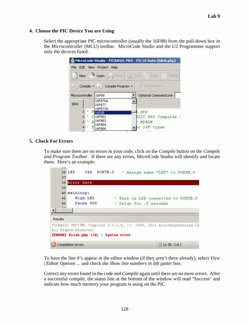
Lab 9
128
4. Choose the PIC Device You are Using
Select the appropriate PIC microcontroller (usually the 16F88) from the pull-down box inthe Microcontroller (MCU) toolbar. MicroCode Studio and the U2 Programmer supportonly the devices listed.
5. Check For Errors
To make sure there are no errors in your code, click on the Compile button on the Compileand Program Toolbar. If there are any errors, MicroCode Studio will identify and locatethem. Here’s an example:
To have the line #’s appear in the editor window (if they aren’t there already), select View| Editor Options ... and check the Show line numbers in left gutter box.
Correct any errors found in the code and Compile again until there are no more errors. Aftera successful compile, the status line at the bottom of the window will read "Success" andindicate how much memory your program is using on the PIC.
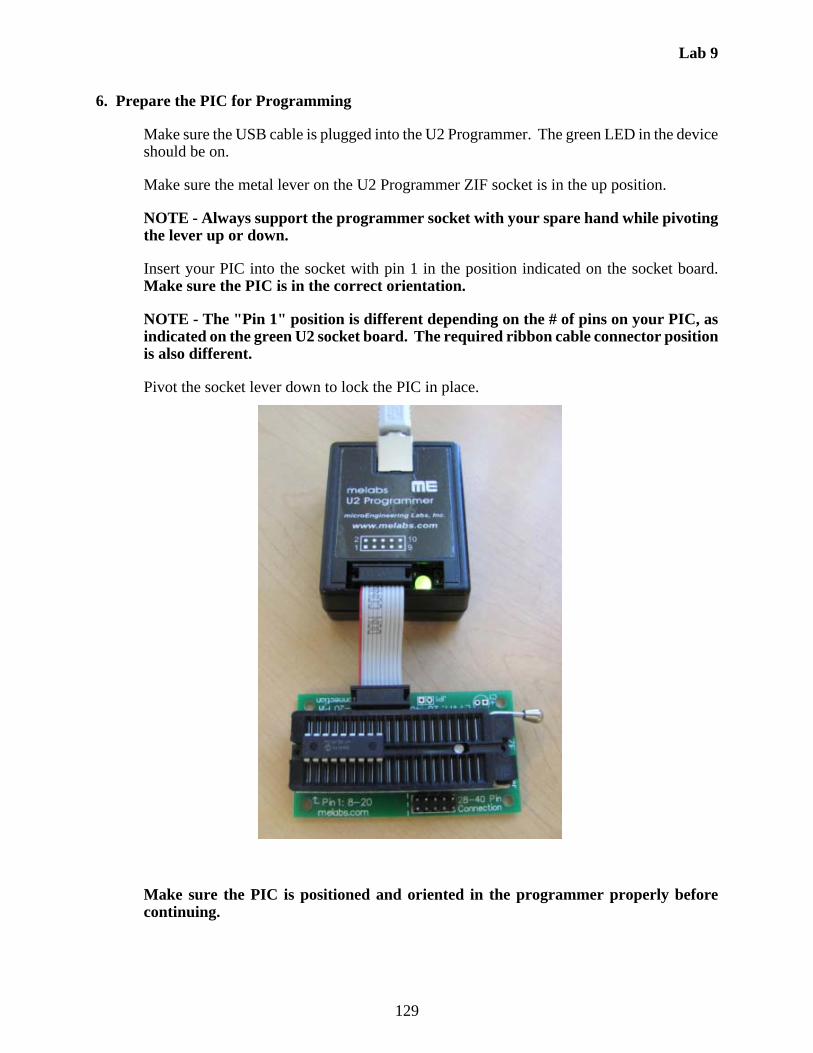
Lab 9
129
6. Prepare the PIC for Programming
Make sure the USB cable is plugged into the U2 Programmer. The green LED in the deviceshould be on.
Make sure the metal lever on the U2 Programmer ZIF socket is in the up position.
NOTE - Always support the programmer socket with your spare hand while pivotingthe lever up or down.
Insert your PIC into the socket with pin 1 in the position indicated on the socket board.Make sure the PIC is in the correct orientation.
NOTE - The "Pin 1" position is different depending on the # of pins on your PIC, asindicated on the green U2 socket board. The required ribbon cable connector positionis also different.
Pivot the socket lever down to lock the PIC in place.
Make sure the PIC is positioned and oriented in the programmer properly beforecontinuing.
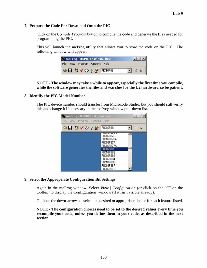
Lab 9
130
7. Prepare the Code For Download Onto the PIC
Click on the Compile Program button to compile the code and generate the files needed forprogramming the PIC.
This will launch the meProg utility that allows you to store the code on the PIC. Thefollowing window will appear:
NOTE - The window may take a while to appear, especially the first time you compile,while the software generates the files and searches for the U2 hardware, so be patient.
8. Identify the PIC Model Number
The PIC device number should transfer from Microcode Studio, but you should still verifythis and change it if necessary in the meProg window pull-down list.
9. Select the Appropriate Configuration Bit Settings
Again in the meProg window, Select View | Configuration (or click on the "C" on thetoolbar) to display the Configuration window (if it isn’t visible already).
Click on the down-arrows to select the desired or appropriate choice for each feature listed.
NOTE - The configuration choices need to be set to the desired values every time yourecompile your code, unless you define them in your code, as described in the nextsection.
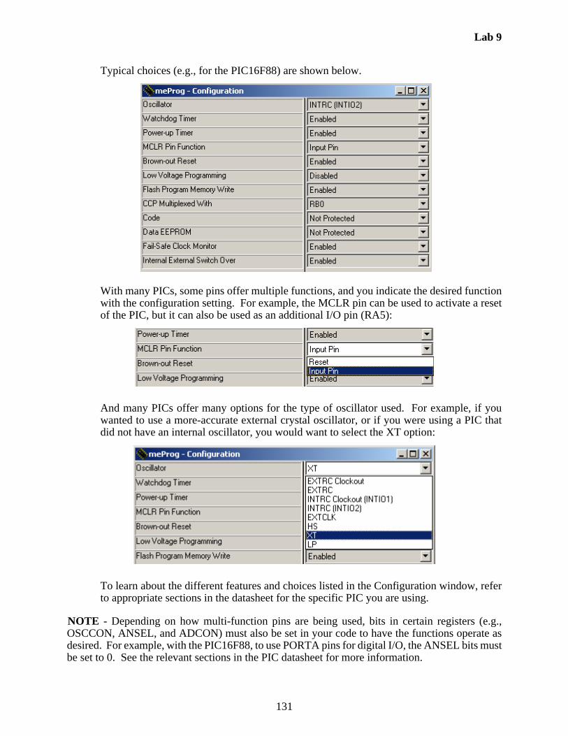
Lab 9
131
Typical choices (e.g., for the PIC16F88) are shown below.
With many PICs, some pins offer multiple functions, and you indicate the desired functionwith the configuration setting. For example, the MCLR pin can be used to activate a resetof the PIC, but it can also be used as an additional I/O pin (RA5):
And many PICs offer many options for the type of oscillator used. For example, if youwanted to use a more-accurate external crystal oscillator, or if you were using a PIC thatdid not have an internal oscillator, you would want to select the XT option:
To learn about the different features and choices listed in the Configuration window, referto appropriate sections in the datasheet for the specific PIC you are using.
NOTE - Depending on how multi-function pins are being used, bits in certain registers (e.g.,OSCCON, ANSEL, and ADCON) must also be set in your code to have the functions operate asdesired. For example, with the PIC16F88, to use PORTA pins for digital I/O, the ANSEL bits mustbe set to 0. See the relevant sections in the PIC datasheet for more information.

Lab 9
132
10. Changing Configuration Settings in Code
An alternative to setting the configuration bits manually, as described in the previoussection, is to set them within your program.
You only need to add code for the settings for which the default values are different fromwhat you want.
For example, you can automatically achieve the settings shown in the previous section forthe PIC16F88, by adding the following code to your program (or by using the code templateon the Lab book website that already contains the code):
#CONFIG __CONFIG _CONFIG1, _INTRC_IO & _PWRTE_ON & _MCLR_OFF & _LVP_OFF#ENDCONFIG
Note that there are two underscores in front of the "CONFIG" and only one underscore infront of the "CONFIG1." There is also a comma between "CONFIG1" and the settings. Allsettings, including any that might be added, are separated by the bitwise AND operator (&).
The settings available for a given PIC can be found in the appropriate *.INFO file for thedevice. These files can be found in: C:\PBP3\DEVICE_REFERENCE.
11. Download Your Code Onto the PIC
After all of the configuration choices have been set to the desired values, click on theProgram icon
or select Program from the Program menu in the meProg window.
The U2 programmer LED will glow red while the code is being downloaded, and it shouldglow green again when the process is completed.
After the program is written and verified, a Program Verify complete dialog box shouldappear, indicating that everything worked properly. Click on OK.
NOTE - Never insert or remove a PIC when the LED glows red. This can causedamage to the chip and/or the programmer.
12. Remove and Test the Programmed PIC
Lift the lever on the programmer to release the pin clamp. Then remove the PIC from thesocket and insert it into your circuit for testing.
13. Shutdown the Software and Logoff
Close (Exit) the MicroCode Studio application. The programmer and configurationwindows will close automatically with MicroCode Studio.
Be sure to log off your session on the PC so others won’t use (and/or abuse) your account.

Lab 9
133
9.5 Using Interrupts
An interrupt is a specially designated input to a microcontroller that changes the sequenceof execution of a program. When there is a change of state of one or more of the input pinsdesignated as interrupts, the program pauses normal execution and jumps to separate code calledan interrupt service routine. When the service routine terminates, normal program executionresumes with the statement following the point where the interrupt occurred. The interrupt serviceroutine is identified by the PICBasic ON INTERRUPT GOTO command. An example programcalled onint.bas follows:
' onint.bas' Example use of an interrupt signal and interrupt handler' This program turns on an LED and waits for an interrupt on PORTB.0. When RB0 changes ' state, the program turns the LED off for 0.5 seconds and then resumes normal execution.
' Identify and set the internal oscillator clock speed (required for the PIC16F88)DEFINE OSC 8OSCCON.4 = 1OSCCON.5 = 1OSCCON.6 = 1
' Turn off the A/D converter (required for the PIC16F88)ANSEL = 0
led var PORTB.7 ' define variable led
OPTION_REG = $FF ' disable PORTB pull-ups and detect positive edges on interrupt On Interrupt Goto myint ' define interrupt service routine location INTCON = $90 ' enable interrupt on pin RB0
' Turn LED on and keep it on until there is an interruptmyloop:
High led Goto myloop
' Interrupt handler Disable ' do not allow interrupts below this pointmyint:
Low led ' if we get here, turn LED off Pause 500 ' wait 0.5 seconds INTCON.1 = 0 ' clear interrupt flag Resume ' return to main program Enable ' allow interrupts again
End ' end of program
The onint.bas program turns on an LED using PORTB.7 until an external interrupt occurs.A switch or button connected to pin 6 (PORTB.0) provides the source for the interrupt signal.

Lab 9
134
When the signal transitions from low to high, the interrupt routine executes, causing the LED toturn off for half a second. Control then returns to the main loop causing the LED to turn back onagain. More detail is provided in the following paragraphs.
NOTE: when using constants in a program, the dollar sign ($) prefix indicates a hexadecimal valuepercent sign (%) prefix indicates a binary value.
The first active line uses the keyword var to create the variable name led to denote the pinidentifier PORTB.7. In the next line the OPTION_REG is set to $FF (or %11111111) to disablePORTB pull-ups and to configure the interrupt to be triggered when a positive edge occurs on pinRB0. When pull-ups are enabled, the PORTB inputs are held high until they are driven low by theexternal input circuit (e.g., a switch or button wired to pin RB0). The option register is defined inmore detail below.
The label "myint" is defined as the location to which the program control jumps when aninterrupt occurs. The value of the INTCON register is set to $90 (or %10010000) to properlyenable interrupts. Setting the INTCON.7 bit to 1 globally allows all interrupts, and setting theINTCON.4 bit to 1 specifically enables the PORTB.0 interrupt. The INTCON register is describedin more detail below.
The two lines starting with "loop" label cause the program to continually maintain the ledpin (PORTB.7) high which keeps the LED on. The continuous cycle created by the "Goto loop"statement is called an infinite loop since it runs as long as no interrupt occurs. Note that an activestatement (such as: "High led") MUST exist between the label and Goto of the loop for the interruptto function because PICBASIC checks for interrupts only after a statement is completed.
The final section of the program contains the interrupt service routine. Disable mustprecede the label (myint:) and Enable must follow the Resume to prevent further interrupts fromoccurring until control is returned to the main program. The placement of these commands mightseem awkward if you think about it, but this is the correct syntax. The interrupt routine executeswhen control of the program is directed to the beginning of this routine (labeled by "myint:") whenan interrupt occurs on PORTB.0 (pin 6). At the identifier label "myint" the statement Low led setsPORTB.7 (pin 13) to a digital low turning off the LED in the circuit. The Pause statement causesa 500 milliseconds (half a second) delay, during which the LED remains off. The next line sets theINTCON.1 bit to zero to clear the interrupt flag. The interrupt flag was set internally to 1 when theinterrupt signal was received on PORTB.0, and this bit must be reset to zero before exiting theinterrupt routine. At the end of the myint routine, control returns back to the main program loopwhere the interrupt occurred.
Lab 9
135
9.5.1 Registers Related to Interrupts
In order to detect interrupts, two specific registers on the PIC must be initialized correctly.These are the option register (OPTION_REG) and the interrupt control register (INTCON). Thefunction of the individual bits within both registers are defined below.
The definition for each bit in the first register (OPTION_REG) follows. Recall that theleast significant bit (LSB) is on the right, and is designated as bit zero (b0), while the mostsignificant bit (MSB) is on the left, and is designated as bit 7 (b7).
OPTION_REG = %b7b6b5b4b3b2b1b0
bit 7: RBPU: PORTB Pull-up Enable Bit1 = PORTB pull-ups are disabled0 = PORTB pull-ups are enabled (by individual port latch values)
bit 6: Interrupt Edge Select Bit1 = Interrupt on rising edge of RB0/INT pin0 = Interrupt on falling edge of RB0/INT pin
bit 5: T0CS: TMR0 Clock Source Select Bit1 = Transition on RA4/TOCK1 pin0 = Internal instruction cycle clock (CLKOUT)
bit 4: T0SE: TMR0 Source Edge Select Bit1 = Increment on high-to-low transition on RA4/TOCK1 pin0 = Increment on low-to-high transition on RA4/TOCK1 pin
bit 3: PSA: Prescaler Assignment Bit1 = Prescaler assigned to the Watchdog timer (WDT)0 = Prescaler assigned to TMR0
bits 2-0:PS2: PS0: Prescaler Rate Select BitsBit Value TMR0 Rate WDT Rate000 1 : 2 1 : 1001 1 : 4 1 : 2010 1 : 8 1 : 4011 1 : 16 1 : 8100 1 : 32 1 : 16101 1 : 64 1 : 32110 1 : 128 1 : 64111 1 : 256 1 : 128
In the onint.bas example above, OPTION_REG was set to $FF which is %11111111.Setting bit 7 high disables PORTB pull-ups and setting bit 6 high causes interrupts to occur on thepositive edge of a signal on pin RB0. Bits 0 through 5 are only important when using special timersand are not used in this example.

Lab 9
136
The definition for each bit in the second register (INTCON) follows:
bit 7: GIE: Global Interrupt Enable Bit1 = Enables all unmasked interrupts0 = Disables all interrupts
bit 6: EEIE: EE Write Complete Interrupt Enable Bit1 = Enables the EE Write Complete interrupt0 = Disables the EE Write Complete interrupt
bit 5: T0IE: TMR0 Overflow Interrupt Enable Bit1 = Enables the TMR0 interrupt0 = Disables the TMR0 interrupt
bit 4: INTE: RB0/INT Interrupt Enable Bit1 = Enables the RB0/INT interrupt0 = Disables the RB0/INT interrupt
bit 3: RBIE: RB Port Change Interrupt Enable Bit (for pins RB4 through RB7)1 = Enables the RB Port Change interrupt0 = Disables the RB Port Change interrupt
bit 2: T0IF: TMR0 Overflow Interrupt Flag Bit1 = TMR0 has overflowed (must be cleared in software)0 = TMR0 did not overflow
bit 1: INTF: RB0/INT Interrupt Flag Bit1 = The RB0/INT interrupt occurred0 = The RB0/INT interrupt did not occur
bit 0: RBIF: RB Port Change Interrupt Flag Bit1 = When at least one of the RB7:RB4 pins changed state (must be cleared in software)0 = None of the RB7:RB4 pins have changed state
In the onint.bas example above, INTCON was set to $90 which is %10010000. For interrupts tobe enabled, bit 7 must be set to 1. Bit 4 is set to 1 to check for interrupts on pin RB0. Bits 6, 5, 3,and 2 are for advanced features and are not used in this example. Bits 0 and 1 are used to indicatedinterrupt status during program execution.
If more than one interrupt signal were required, bit 3 would be set to 1 which would enableinterrupts on pins RB4 through RB7. In that case, INTCON would be set to $88 (%10001000). Tocheck for interrupts on RB0 and RB4-7, INTCON would be set to $98 (%10011000). PORTA hasno interrupt capability, and PORTB has interrupt capability only on pins RB0 and pins RB4through RB7.
NOTE - PicBasicPro does not handle interrupts very efficiently, and the codecan be confusing. Hardware interrupts can be very effective when usingAssembly language or C, but PicBasicPro software interrupts should usually beavoided. It is better to just use polling loops instead (see the next Lab for moreinfo).

Lab 9
137
9.6 Procedure
(1) Use an ASCII editor (e.g., Windows Notepad or MS Word - Text Only) to create theprogram "blink.bas" listed in Section 9.3. Save the file in a folder in your networkfile space.
(2) Follow the procedure in Section 9.4 to compile the "blink.bas" program intohexadecimal machine code ("blink.hex") and to load this code onto a PIC.
(3) Assemble and test the circuit shown in Figure 9.1. When power is applied, the LEDshould immediately begin to blink on and off, cycling once each second.
(4) Repeat steps (1) through (2) for the "onint.bas" program listed in Section 9.5. Be sureto create a new project and follow the entire procedure. Before constructing thecircuit for onint.bas, identify the additional components required in Figure 9.2.Indicate the necessary changes in the figure and check with your Teaching Assistantto verify that your changes are appropriate. The program should turn on an LEDattached to PORTB.7. An interrupt on PORTB.0 should cause the LED to turn offfor half a second, and then turn back on again. This should be signaled by an singlepole, single throw (SPST) switch or a normally open (NO) button. You must makesure to wire the switch or button such that the ON state applies 5 Vdc to the pin, andthe OFF state grounds the pin. The input should not be allowed to "float" in the OFFstate (i.e., it must be grounded through a 1k resistor). When you are sure you haveall components wired properly, apply power to the circuit and test it to determine if itis working properly.
NOTE - When removing ICs from a breadboard,always use a "chip puller" tool to lift both endstogether. Alternatively, use a small flat-headscrewdriver to pry each end up a little at a time torelease the IC without causing damage (e.g., bent orbroken pins).
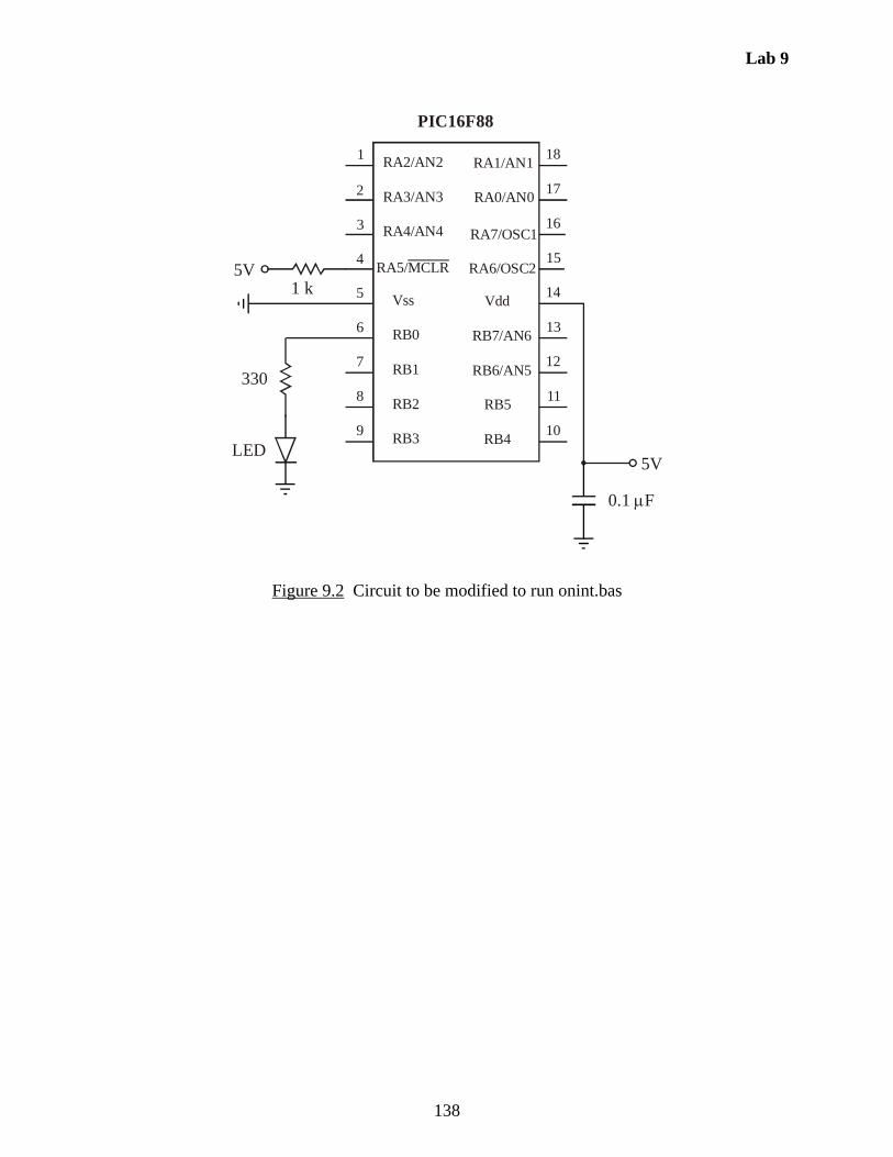
Lab 9
138
Figure 9.2 Circuit to be modified to run onint.bas
PIC16F88
RA2/AN2
RA3/AN3
RA4/AN4
RA5/MCLR
Vss
RB0
RB1
RB2
RB3
RA1/AN1
RA0/AN0
RA7/OSC1
RA6/OSC2
Vdd
RB7/AN6
RB6/AN5
RB5
RB4
1
2
3
4
5
6
7
8
9 10
11
12
13
14
15
16
17
18
5V1 k
5V
0.1 F
330
LED

Lab 9
139
LAB 9 QUESTIONS
Group: ____ Names: _________________________ _____________________________
_________________________ _____________________________
(1) Explain all differences between PORTA and PORTB if using the pins for inputs. Refer toSection 7.8 in the textbook for more information.
(2) For the onint.bas interrupt example, if the button is held down for more that 0.5 second andthen released, is it possible that the LED would blink off again? If so, explain why. (Hint:consider switch bounce.)
(3) Show two different ways to simply and properly interface an LED to a PIC output pin. Onecircuit should light the LED only when the pin is high (this is called positive logic) and theother circuit should light the LED only when the pin is low (this is called negative logic).

Lab 9
140
(4) Explain what you would observe if power were applied to a PIC loaded with the followingcode if an LED is connected to RB0 as shown in Figure 9.1. Note - Goto is being used, notGosub.
before: High PORTB.0Pause 500Low PORTB.0Goto duringPause 100High PORTB.0Goto after
during:Low PORTB.0Pause 300High PORTB.0Pause 400
after: Pause 200Low PORTB.0End

Lab 10
141
Laboratory 10
Programming a PIC Microcontroller - Part II
Required Components:• 1 PIC16F88 18P-DIP microcontroller• 1 0.1 F capacitor• 3 SPST microswitches or NO buttons• 4 1k resistors• 1 MAN 6910 or LTD-482EC seven-segment LED digital display• 1 330 DIP resistor array
Required Special Equipment and Software:
• Mecanique’s Microcode Studio integrated development environment software
• MicroEngineering Labs’ PicBasic Pro compiler
• MicroEngineering Labs’ U2 USB Programmer• Demonstration hexadecimal counter circuit board containing a 555 timer circuit and a
D flip-flop latch IC
10.1 Objective
This laboratory exercise builds upon the introduction to the PIC microcontroller started inthe previous Lab. Here, input polling is introduced as an alternative to interrupts. You will learnhow to configure and control the inputs and outputs of the PIC using the TRIS registers. You willalso learn how to perform logic in your programs. You will first observe and describe the operationof a hexadecimal counter project demonstrated in the video on the Lab website. You will thencreate and test an alternative design using different hardware and software.
10.2 Hexadecimal Counter Using Polling
The first part of the laboratory involves the demonstration of an existing counting circuitusing a PIC to activate the 7 segments of a digital LED display. You will not be building a circuitor writing code for this demonstration design; although, the alternative design you willimplement has some similarities. At power-up of the demo circuit, a zero is displayed, and threeseparate buttons are used to increment by one, decrement by one, or reset the display to zero. Thedisplay is hexadecimal so the displayed count can vary from 0 to F. An input monitoring techniquecalled polling is used in this example. With polling, the program includes a loop that continuallychecks the values of specific inputs. The output display is updated based on the values of theseinputs. Polling is different from interrupts in that all processing takes place within the mainprogram loop, and there is not a separate interrupt service routine. Polling has a disadvantage thatif the program loop takes a long time to execute (e.g., if it performs complex control calculations),changes in the input values may be missed. The main advantage of polling is that it is very easy toprogram.

Lab 10
142
TRIS Registers
At power-up, all bits of PORTA and PORTB are initialized as inputs. However, in thisexample we require 7 output pins. Here, pins to be used as outputs are designated using specialregisters called the TRISA and TRISB. These registers let us define each individual bit of thePORT as an input or an output. In the previous examples that also required an output, this was notnecessary since the High and Low commands set the TRIS registers automatically. In this examplewe will use assignment statements to set the PORT output values directly (e.g., PORTB =%00011001), requiring setting of the TRIS registers. Most PICBasic commands that use pins asoutputs or inputs automatically set the TRIS register bits to appropriate values.
Setting a TRIS register bit to 0 designates an output and setting the bit to 1 designates aninput. For example,
TRISA = %00000000
designates all bits of PORTA as outputs and
TRISB = %01110000
designates bits 4, 5, and 6 of PORTB as inputs and the others as outputs.
Note that since PORTA has only 5 usable bits (bits 0 through 4), the three most significant bits ofPORTA are ignored and have no effect. At power-up all TRIS register bits are set to 1, so all pinsare treated as inputs by default (i.e., TRISA=$FF and TRISB=$FF).
The code "counter.bas" for the up/down hex counter in listed below. NOTE - You willneed to modify this code, and the circuit, for this Laboratory. See Sections 10.3 and 10.5 formore information.
' counter.bas' PicBasic hex up/down counter
' Identify and set the internal oscillator clock speed (required for the PIC16F88)DEFINE OSC 8OSCCON.4 = 1OSCCON.5 = 1OSCCON.6 = 1
' Turn off the A/D converter (required for the PIC16F88)ANSEL = 0
' Declare variablespins var byte[16] ' an array of 16 bytes used to store the 7-segment display codesI var byte ' counter variable

Lab 10
143
' Initialize I/O pinsTRISA = %00000000 ' all PORTA pins initialized as outputs
' (although only pins 0, 1, and 2 are used)TRISB = %01110000 ' PORTB.4,5,6 pins initialized as inputs
' (RB4: reset, RB5: increment, RB6: decrement)' all other PORTB pins initialized as outputs
' Initialize the pin values for the 7-segment LED digit display with segments as illustrated below' a' -------' | |' f | | b' | g |' -------' | |' e | | c' | |' -------' d
' Three of the pins in PORTA and four of the pins in PORTB are used as the seven outputs.' The LED segments are assigned to the PORT bits as shown below:' PORTA PORTB' bit number: 76543210 76543210' segment: -----cde ----bagf
' The PORT pin numbers (on the PIC pin-out) correspond to the PORT bit numbers as follows:' LED segment: e d c' PORTA bit: 0 1 2' PORTA pin name: RA0 RA1 RA2' PORTA pin number: 17 18 1
' LED segment: f g a b' PORTB bit: 0 1 2 3' PORTB pin name: RB0 RB1 RB2 RB3' PORTB pin number: 6 7 8 9
' NOTE: 0 turns a segment ON and 1 turns it OFF since the PIC sinks current from the LED display' binary hex display' %0cdebagf (correspondence between LED segments and pins array bits)pins[ 0] = %00000010 ' 02 0pins[ 1] = %00110111 ' 37 1pins[ 2] = %01000001 ' 41 2pins[ 3] = %00010001 ' 11 3pins[ 4] = %00110100 ' 34 4pins[ 5] = %00011000 ' 18 5pins[ 6] = %00001000 ' 08 6

Lab 10
144
pins[ 7] = %00110011 ' 33 7pins[ 8] = %00000000 ' 00 8pins[ 9] = %00110000 ' 30 9pins[10] = %00100000 ' 20 Apins[11] = %00001100 ' 0C bpins[12] = %01001010 ' 4A Cpins[13] = %00000101 ' 05 dpins[14] = %01001000 ' 48 Epins[15] = %01101000 ' 68 F' %0cdebagf (correspondence between LED segments and pins array bits)
' Initialize the display to zeroI = 0Gosub Updatepins
' Main loopmyloop:
If (PORTB.4 == 1) Then ' reset I = 0 Gosub Updatepins Pause 100 ' 0.1 sec delay Endif
If (PORTB.5 == 1) Then ' increment If (I == 15) Then I = 0 Else I = I + 1 Endif
Gosub Updatepins Pause 100 ' 0.1 sec delay Endif
If (PORTB.6 == 1) Then ' decrement If (I == 0) Then I = 15 Else I = I - 1 Endif
Gosub Updatepins Pause 100 ' 0.1 sec delay Endif
Goto myloop ' go back to the beginning of the loop and continue to poll the inputs

Lab 10
145
' Updatepins Subroutine' sends new output values to pins
Updatepins: ' Use the right shift operator to move the top MSB’s of pins[I] to the 4 LSB’s of PORTA ' padding the 4 MSBs of PORTA with 0’s PORTA = pins[I] >> 4 ' Use logic to retain the 4 MSB’s of PORTB and replace the 4 LSB’s of PORTB by ' by the 4 LSB’s of pins[I] PORTB = (PORTB | %00001111) & (pins[I] | %11110000) Return
End ' End of program
After the initial comments labeling the program, the pins variable is defined as an array of16 bytes. Elements in the array are accessed by the syntax pins[I], where I is the index havingvalues from 0 through 15. Binary values for the pins array elements are set in the "Initialize thepin values ..." section. The mapping of these bits to individual segments on the 7-segment counterdisplay, and the structure of the counter circuit dictates the assignment of each of these bits to aspecific segment. The 8 bits in each byte are grouped into 2 sets of 4 bits: the left 4 bits (mostsignificant bits: MSB’s) assign values to the pins set by PORTA, and the right 4 bits (leastsignificant bits: LSB’s) assign values to the pins set by PORTB. Again, these depend on thefunction of the circuit attached to the PIC. Bits 4, 5, and 6 of the pins[I] variable are output throughPORTA pins to segments e, d, and c of the display, respectively. Bits 0, 1, 2, and 3 of the pins[I]variable are output through PORTB pins to segments f, g, a, and b of the display, respectively. Notethat bit 7 is set to 0 for each element in the pins[I] variable. Also, note that bit values assumenegative logic where a 0 turns the segment on and a 1 turns the segment off.
The TRIS registers are set to determine the I/O status of the pins in PORTA and PORTB.Since all bits in TRISA are 0, all pins corresponding to PORTA are set as outputs. Note thatPORTA bits 5, 6, and 7 have no function since no pins actually exist on the PIC to correspond tothese values. The TRISB register value is set so that PORTB bits 4, 5, and 6 are inputs (each ofthese 3 bits is set to 1), while the other 5 pins of PORTB are set as outputs. Each of these threeinput pins for PORTB is attached to a separate button. Depending upon which button is pressed,the counter will either increment by one, decrement by one, or reset to zero using the hexadecimalcounting sequence.
The polling loop used to check for button input is in the "Main loop" of the program. Thefirst IF statement checks whether the button attached to PORTB.4 is down. If it is, the index forthe pins[I] variable is set to 0 so that the display will be zero. The Updatepins routine is called toupdate the value displayed as described in detail below. Then a pause occurs for 100 milliseconds(0.1 sec). The polling then continues by checking PORTB.5, and if the value is high, then thehexadecimal count is incremented by incrementing the index for the pins[I] variable. Theinternally nested IF statement checks if the index exceeds the allowed value of 15, and if it doesthe index is reset to 0. The display effectively will count from 0 through 15 as the button isrepeatedly depressed or held down, but will cycle back to 0 after an F has been displayed (thehighest digit value in hexadecimal). Again a call to Updatepins updates the display, and a 0.1second pause occurs. The pause prevents the count from updating too quickly while the button is

Lab 10
146
being held down before it is released. If the button is held down for more than 0.1 second thecounter will increment every 0.1 second. Then PORTB.6 is checked and a value of 1 will cause adecrement in the index for the pins[I] variable. Once the display reaches a minimum value of zero,the routine will cycle back to F for the next hexadecimal value.
The most direct action in displaying the output occurs in the Updatepins routine. A simpleassignment statement (a statement containing an equal sign =) performs the write to the pins thatchange the segments in the display. Recall that only three of the five available output pins are usedon PORTA (the LSB’s of PORTA). Since the pins[I] variable stores values for PORTA in bits 4through 7 (the MSB’s of pins[I]), these bits must be extracted and shifted. The right shift operator(>>) is used to shift the four MSB’s four places to the right to become the four LSB bits 0 through3. The four MSB’s are replaced with 0’s as a result of the shift. The result is written to PORTAby the assignment statement. Output to PORTB is more complex since the procedure seeks tomaintain the existing values for bits 4 through 7 (the MSB’s of PORTB) since these bits arereserved for the button inputs, while changing bits 0 through 3 (the LSB’s of PORTB). Booleanlogic operators for OR (|) and AND (&) are used to carry out this process. The OR in the left setof parentheses maintains the four MSB’s of PORTB, and sets the four LSB’s to 1. The OR in theright set of parentheses maintains the four LSB’s of the pins[I] variable, and sets the four MSB’sto 1. When the two results are ANDed, the four MSB’s of PORTB are maintained, while the fourLSB’s are changed to the values found in the currently indexed pins[I] element. The assignmentto PORTB effectively writes the LSB’s to the pins, which turns the respective segments on or off.The display is updated every time a call is made to the Updatepins routine.
As shown in Figure 10.1, latching of button values is accomplished by the use of D flip-flops (74LS175) in the circuit. Also key to the circuit, but not shown in the figure, is the use of a555 timer circuit to create a 100 Hz clock signal. On each positive edge of clock pulse, the currentstates of the buttons are stored (latched) in the D flip-flips on the 74LS175 IC. Together, the timerand flip-flops perform a hardware debounce. The latched values are read by the PIC each time theprogram passes through the polling loop. Note that the buttons are shown wired in the figure withnegative logic, where the button signal is normally high and goes low when it is pressed. The
software above assumes positive logic (with the aide of the outputs on the D flip-flops) insteadwhere the button signal is normally low and goes high when pressed. This is easily accomplishedby using a pull-down resistor to ground instead of a pull-up resistor to 5V.
Again, you will not be building the circuit shown in Figure 10.1. You will just view avideo demonstration of the working circuit on the Lab website.
Q

Lab 10
147
NOTE - Do not build this circuit. You will build an alternative design instead (see Sections 10.3 and 10.5).
Figure 10.1 Circuit Diagram for the Demonstration-Only Hexadecimal Counter
NOTE:These resistorsare on a DIP IC.

Lab 10
148
10.3 An Alternative Design
The hardware and software design in the previous section can be simplified if you usePORTA for the three button inputs and PORTB for all seven of the LED segment outputs. Thiswas not done for the example above since the hardware was originally designed and built by agraduate student assuming hardware interrupts would be used. Hardware interrupts are availableonly in PORTB, and if the three buttons were attached to PORTB, only five bits in PORTB wouldbe available to be used as outputs. Furthermore, on the PIC16F84, PORTA only has five bitsavailable. Because we need seven bits to drive the display, both PORTA and PORTB were usedfor the seven outputs.
An alternative design is outlined below using PORTB for all seven outputs and PORTA forthe three inputs. This dramatically simplifies the Updatepins subroutine eliminating the need forthe complex logic manipulations of the bits. The changes required to the hardware and software forthe alternative design follow.
The bits in PORTB are assigned and connected to the LED segments as follows:
bit number: %76543210 segment: %-cdebagf
The TRIS registers are initialized as follows:
TRISA = %00001110 ' PORTA.1,2,3 pins are inputsTRISB = %00000000 ' all PORTB pins are outputs (although, pin 7 is not used)
Then the simpler Updatepins subroutine is:
Updatepins: PORTB = pins[I] Return
where the bit values in the pins[I] array element are written directly to the PORTB bits driving theLED segments.
Switch debounce can be performed in software instead of hardware eliminating the needfor the 555 timer and D flips-flop portions of the demonstration circuit. Figure 10.2 shows thehardware for the alternative design (using bits 1,2, and 3 on PORTA). Be sure to wire the switchwith pull-down resistors for positive logic.
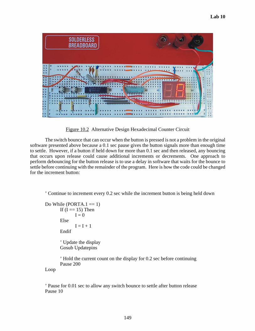
Lab 10
149
Figure 10.2 Alternative Design Hexadecimal Counter Circuit
The switch bounce that can occur when the button is pressed is not a problem in the originalsoftware presented above because a 0.1 sec pause gives the button signals more than enough timeto settle. However, if a button if held down for more than 0.1 sec and then released, any bouncingthat occurs upon release could cause additional increments or decrements. One approach toperform debouncing for the button release is to use a delay in software that waits for the bounce tosettle before continuing with the remainder of the program. Here is how the code could be changedfor the increment button:
’ Continue to increment every 0.2 sec while the increment button is being held down
Do While (PORTA.1 == 1)If (I == 15) Then
I = 0Else
I = I + 1Endif
’ Update the displayGosub Updatepins
’ Hold the current count on the display for 0.2 sec before continuingPause 200
Loop
’ Pause for 0.01 sec to allow any switch bounce to settle after button releasePause 10

Lab 10
150
The decrement button would be handled in a similar fashion. No debounce is required forthe reset button because multiple resets in a short period of time (e.g., the few thousandths of asecond when bouncing occurs) do not result in undesirable behavior.
Yet another alternative design that would further simplify the software would be to use a7447 IC for BCD-to-7-segment decoding. This would eliminate the need for the pins array thatdoes the decoding in software, but it would add an additional IC to the hardware design. Also, the7447 displays non-alphanumeric symbols for digits above 9, instead of the hexadecimal characters(A, b, C, d, E) that we control with the pins array.
10.4 PIC Circuit Debugging Recommendations
It is rare that a wired PIC circuit works the first time it is tested. Often there are "bugs" withthe software or the wiring. Here are some recommendations that can help you when trying to geta PIC circuit to function (e.g., with your project):
(1) If you are using a PIC that requires an external oscillator (e.g, the PIC16F84x), makesure your circuit includes the necessary clock crystal and capacitor components. Ifyou are using a PIC with an internal oscillator (e.g., the PIC16F88), make sure youinclude the necessary initialization code (e.g., see the code template for the PIC16F88available on the Lab website).
(2) If you use MS Word or other word processor to edit your code, make sure you "SaveAs" a text file, or just copy and paste your code from the word processor into theMicroCode Studio or MPLAB editor.
(3) Make sure your wiring is very neat (i.e., not a "rats nest"), keep all of your wires asshort as possible to minimize electrical magnetic interference (EMI) (and addedresistance, inductance, and capacitance), and use appropriate lengths (about 1/4") forall exposed wire ends (to help prevent breadboard damage and shorting problems).
(4) Follow all of the recommendations in Section 7.4 for prototyping IC circuits.
(5) Be very gentle with the breadboards. Don’t force wires into or out of the holes. Ifyou do this, the breadboard might be damaged and you will no longer be able to createreliable connections in the damaged holes or rows.
(6) Make sure all components and wires are firmly seated in the breadboard, establishinggood connections (especially with larger PICs you might use in your projects). Youcan check all of your connection with the beep continuity feature on a multimeter.
(7) Before writing and testing the entire code for your project, start with the BLINKprogram in Lab 9 to ensure your PIC is functioning properly. Then incrementally addand test portions of your code one functional component at a time.
(8) Use a "chip puller" (small tool) to remove PICs and other ICs from the breadboard toprevent damage (i.e., bent or broken pins).
(9) Always use the PIC programming procedure in Section 9.4 of the previous Labto ensure you don’t miss any important steps or details.
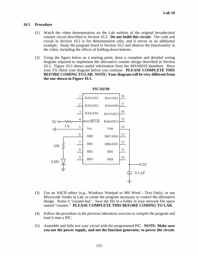
Lab 10
151
10.5 Procedure
(1) Watch the video demonstration on the Lab website of the original hexadecimalcounter circuit described in Section 10.2. Do not build this circuit. The code andcircuit in Section 10.2 is for demonstration only, and it serves as an additionalexample. Study the program listed in Section 10.2 and observe the functionality inthe video, including the effects of holding down buttons.
(2) Using the figure below as a starting point, draw a complete and detailed wiringdiagram required to implement the alternative counter design described in Section10.3. Figure 10.3 shows useful information from the MAN6910 datasheet. Haveyour TA check your diagram before you continue. PLEASE COMPLETE THISBEFORE COMING TO LAB. NOTE: Your diagram will be very different fromthe one shown in Figure 10.1.
(3) Use an ASCII editor (e.g., Windows Notepad or MS Word - Text Only), or useMicrocode Studio in Lab, to create the program necessary to control the alternativedesign. Name it "counter.bas". Save the file in a folder in your network file spacenamed "counter." PLEASE COMPLETE THIS BEFORE COMING TO LAB.
(4) Follow the procedure in the previous laboratory exercise to compile the program andload it onto a PIC.
(5) Assemble and fully test your circuit with the programmed PIC. NOTE: Make sureyou use the power supply, and not the function generator, to power the circuit.
PIC16F88
RA2/AN2
RA3/AN3
RA4/AN4
RA5/MCLR
Vss
RB0
RB1
RB2
RB3
RA1/AN1
RA0/AN0
RA7/OSC1
RA6/OSC2
Vdd
RB7/AN6
RB6/AN5
RB5
RB4
1
2
3
4
5
6
7
8
9 10
11
12
13
14
15
16
17
18
5V1 k
5V
0.1 F
330
LED
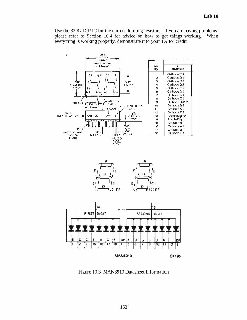
Lab 10
152
Use the 330 DIP IC for the current-limiting resistors. If you are having problems,please refer to Section 10.4 for advice on how to get things working. Wheneverything is working properly, demonstrate it to your TA for credit.
Figure 10.3 MAN6910 Datasheet Information

Lab 10
153
LAB 10 QUESTIONS
Group: ____ Names: _________________________ _____________________________
_________________________ _____________________________
(1) Rewrite "onint.bas" from the previous Lab using polling instead of interrupts.
(2) For the original counter design in Section 10.2, when the 'up' button is held down awhilethe PIC will continue to count up. Explain why.
(3) For the original counter design in Section 10.2, explain what happens when the 'up' and'down' buttons are held down together. Why does this happen?
(4) For the alternative counter design in Section 10.3, why is the 555 and D flip-flop hardwareno longer required?

Lab 10
154
(5) Explain how switch bounce could possibly have a negative impact with the alternativedesign in Section 10.3 if the 0.01 sec software pause were not included.
(6) Explain why debounce software is not required for the reset button in the alternative designin Section 10.3.
(7) For the original counter design in Section 10.2 that was demonstrated in the video (i.e., notthe alternative design in Section 10.3 that you built), how would you create thefunctionality in the Updatepins subroutine for updating the PORTA and PORTB registersusing multiple individual bit references (e.g., PORTA.0 = pins[I].4, PORTA.1 = pins[I].5,...) instead of single-line assignment statements (e.g., PORTA = ... and PORTB = ...)?Hint: The comments above the assignment statements in the code explain what is beingdone.Hint: The comments below the 7-segment-display illustration in the "counter.bas" programinvolving the "bit numbers" and "segments" can be helpful.

Lab 11
155
Laboratory 11
Pulse-Width-Modulation Motor Speed Control with a PIC
Required Components:• 1 PIC16F88 18P-DIP microcontroller• 3 0.1 F capacitors• 1 12-button numeric keypad• 1 NO pushbutton switch• 1 Radio Shack 1.5-3V DC motor (RS part number: 273-223) or equivalent• 1 IRF620 power MOSFET• 1 flyback diode (e.g., the 1N4001 power diode)• 3 1k resistors• 1 2k resistor (or 2 1k resistors)• 1 3k resistor (or 3 1k resistors)• 3 red LEDs• 1 green LED• 4 330 resistors or a 330 8-resistor DIP
Required Special Equipment and Software:• Mecanique’s Microcode Studio integrated development environment software• MicroEngineering Labs’ PicBasic Pro compiler• MicroEngineering Labs’ U2 USB Programmer
11.1 Objective
The objective of this laboratory exercise is to design and build hardware and software toimplement pulse-width modulation (PWM) speed control for a small permanent-magnet dc motor.You will also learn how to interface a microcontroller to a numeric keypad and how to provide anumerical display using a set of LEDs.
11.2 Introduction
Pulse Width Modulation
Pulse width modulation (PWM) offers a very simple way to control the speed of a dcmotor. Figure 11.1 illustrates the principles of operation of PWM control. A dc voltage is rapidlyswitched at a fixed frequency f between two values (“ON” and “OFF”). A pulse of duration toccurs during a fixed period T, where
(11.1)
The resulting asymmetric waveform has a duty cycle defined as the ratio between the ON time andthe period of the waveform, usually specified as a percentage:
(11.2)
T1f---=
duty cycletT---100%=
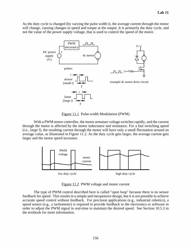
Lab 11
156
As the duty cycle is changed (by varying the pulse width t), the average current through the motorwill change, causing changes in speed and torque at the output. It is primarily the duty cycle, andnot the value of the power supply voltage, that is used to control the speed of the motor.
Figure 11.1 Pulse-width Modulation (PWM)
With a PWM motor controller, the motor armature voltage switches rapidly, and the currentthrough the motor is affected by the motor inductance and resistance. For a fast switching speed(i.e., large f), the resulting current through the motor will have only a small fluctuation around anaverage value, as illustrated in Figure 11.2. As the duty cycle gets larger, the average current getslarger and the motor speed increases.
Figure 11.2 PWM voltage and motor current
The type of PWM control described here is called "open loop" because there is no sensorfeedback for speed. This results in a simple and inexpensive design, but it is not possible to achieveaccurate speed control without feedback. For precision applications (e.g., industrial robotics), aspeed sensor (e.g., a tachometer) is required to provide feedback to the electronics or software inorder to adjust the PWM signal in real-time to maintain the desired speed. See Section 10.5.3 inthe textbook for more information.
DC powersupply
( ) Vs
+
PWMelectronics
dc motor
example dc motor drive circuit
pulses:
slower(small )t
t
T
Vs
T
faster(large )t
t
high duty cycle
PWMvoltage
motorcurrent
low duty cycle
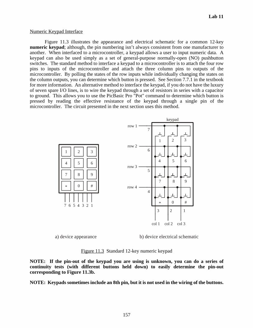
Lab 11
157
Numeric Keypad Interface
Figure 11.3 illustrates the appearance and electrical schematic for a common 12-keynumeric keypad; although, the pin numbering isn’t always consistent from one manufacturer toanother. When interfaced to a microcontroller, a keypad allows a user to input numeric data. Akeypad can also be used simply as a set of general-purpose normally-open (NO) pushbuttonswitches. The standard method to interface a keypad to a microcontroller is to attach the four rowpins to inputs of the microcontroller and attach the three column pins to outputs of themicrocontroller. By polling the states of the row inputs while individually changing the states onthe column outputs, you can determine which button is pressed. See Section 7.7.1 in the textbookfor more information. An alternative method to interface the keypad, if you do not have the luxuryof seven spare I/O lines, is to wire the keypad through a set of resistors in series with a capacitorto ground. This allows you to use the PicBasic Pro "Pot" command to determine which button ispressed by reading the effective resistance of the keypad through a single pin of themicrocontroller. The circuit presented in the next section uses this method.
Figure 11.3 Standard 12-key numeric keypad
NOTE: If the pin-out of the keypad you are using is unknown, you can do a series ofcontinuity tests (with different buttons held down) to easily determine the pin-outcorresponding to Figure 11.3b.
NOTE: Keypads sometimes include an 8th pin, but it is not used in the wiring of the buttons.
1 2 3
4 5 6
7 8 9
* 0 #
7
6
5
4
3 2 1
col 1 col 2 col 3
row 1
row 2
row 3
row 4
keypad
1 2 3
4 5 6
7 8 9
* 0 #
a) device appearance b) device electrical schematic
1234567

Lab 11
158
11.3 Hardware and Software Design
The hardware and software required for this exercise will be designed using themicrocontroller-based design procedure presented in Section 7.9 of the textbook. Each step ispresented below.
(1) Define the problem.
Use a PIC16F84 microcontroller to design a pulse-width modulation speed controllerfor a small permanent magnet dc motor. The user should be able to change the speedvia three buttons of a standard 12-key numeric keypad. One button (the 1-key) shouldincrease the speed setting, a second button (the 4-key) should decrease the speedsetting, and the third button (the *-key) should start the motor at the selected speed.The speed setting should be displayed graphically via a set of 4 LEDs. The speedsetting should vary from "slow" to "fast" according to a scaled number ranging from0 to 15 so the full range can be depicted on the LED display. The motor should runat a constant speed until the motion is interrupted by the user with the press of apushbutton switch.
(2) Draw a functional diagram.
This is left as an exercise for you. Please include it on a separate sheet of paper withyour summary sheet and questions at the end of the Lab. See Section 7.9 in thetextbook for guidance.
(3) Identify I/O requirements.
All inputs and outputs for this problem are digital and they are as follows:
inputs:- 3 buttons on the numeric keypad to increase and decrease the speed and to start themotion.- 1 pushbutton switch to interrupt the constant speed motor motion.
outputs:- 4 LEDs to indicate a relative speed setting from "slow" (0) to "fast" (15) as a binarynumber.- 1 pulse-width modulation (on-off) signal for the motor.
(4) Select an appropriate microcontroller.
For this problem, we will use the PIC16F84 whose 13 lines of digital I/O providemore than enough capability for our I/O requirements.
(5) Identify necessary interface circuits.
To help you learn how to use a numeric keypad in the most efficient way, we willshow you how to connect the rows and columns of the keypad through a network ofresistors in series with a capacitor through a single pin on the PIC. With the help ofthe PICBasic Pro command "Pot," we can determine which button is pressed basedon the time constant of the resulting RC network. The resistance will change basedon which button is pressed. Only a single digital input is required to implement thismethod.
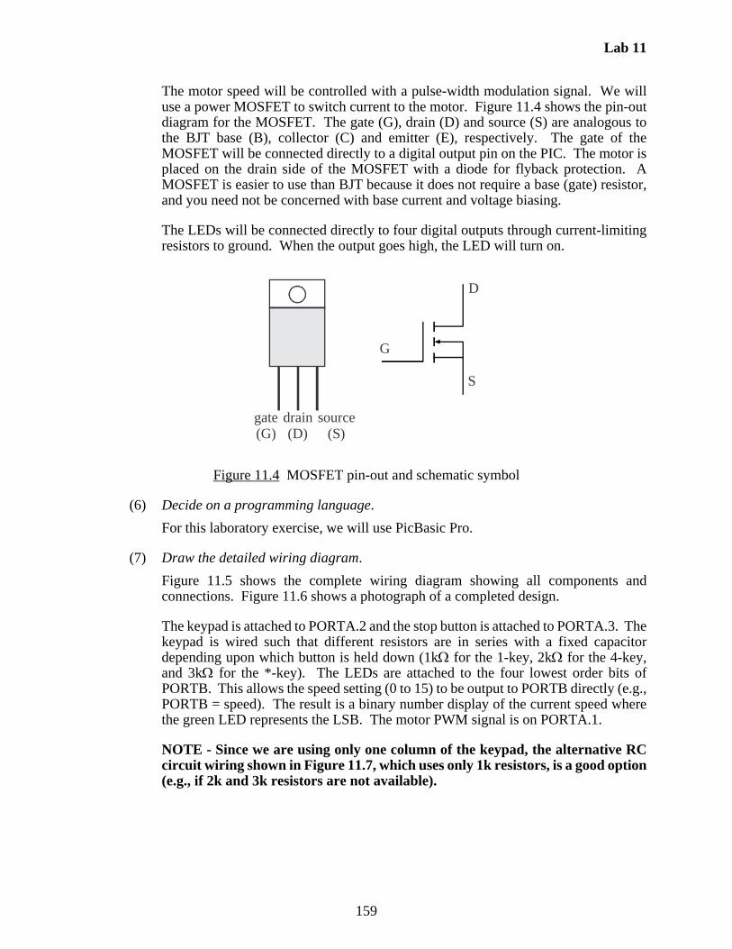
Lab 11
159
The motor speed will be controlled with a pulse-width modulation signal. We willuse a power MOSFET to switch current to the motor. Figure 11.4 shows the pin-outdiagram for the MOSFET. The gate (G), drain (D) and source (S) are analogous tothe BJT base (B), collector (C) and emitter (E), respectively. The gate of theMOSFET will be connected directly to a digital output pin on the PIC. The motor isplaced on the drain side of the MOSFET with a diode for flyback protection. AMOSFET is easier to use than BJT because it does not require a base (gate) resistor,and you need not be concerned with base current and voltage biasing.
The LEDs will be connected directly to four digital outputs through current-limitingresistors to ground. When the output goes high, the LED will turn on.
Figure 11.4 MOSFET pin-out and schematic symbol
(6) Decide on a programming language.
For this laboratory exercise, we will use PicBasic Pro.
(7) Draw the detailed wiring diagram.
Figure 11.5 shows the complete wiring diagram showing all components andconnections. Figure 11.6 shows a photograph of a completed design.
The keypad is attached to PORTA.2 and the stop button is attached to PORTA.3. Thekeypad is wired such that different resistors are in series with a fixed capacitordepending upon which button is held down (1k for the 1-key, 2k for the 4-key,and 3k for the *-key). The LEDs are attached to the four lowest order bits ofPORTB. This allows the speed setting (0 to 15) to be output to PORTB directly (e.g.,PORTB = speed). The result is a binary number display of the current speed wherethe green LED represents the LSB. The motor PWM signal is on PORTA.1.
NOTE - Since we are using only one column of the keypad, the alternative RCcircuit wiring shown in Figure 11.7, which uses only 1k resistors, is a good option(e.g., if 2k and 3k resistors are not available).
gate(G)
drain(D)
source(S)
G
D
S
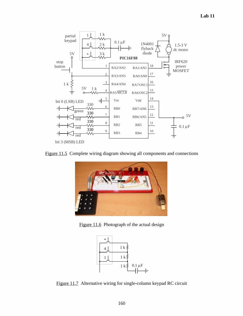
Lab 11
160
Figure 11.5 Complete wiring diagram showing all components and connections
Figure 11.6 Photograph of the actual design
Figure 11.7 Alternative wiring for single-column keypad RC circuit
5V 1 k
5V
0.1 F
5V
stopbutton
1 k
330bit 0 (LSB) LED
330
1.5-3 Vdc motor
5V
330
330330
330330
bit 3 (MSB) LED
0.1 F
1 k
3 k
2 k
1
4
*
partialkeypad
green
red
red
red
IRF620power
MOSFET
1N4001flybackdiode
PIC16F88
RA2/AN2
RA3/AN3
RA4/AN4
RA5/MCLR
Vss
RB0
RB1
RB2
RB3
RA1/AN1
RA0/AN0
RA7/OSC1
RA6/OSC2
Vdd
RB7/AN6
RB6/AN5
RB5
RB4
1
2
3
4
5
6
7
8
9 10
11
12
13
14
15
16
17
18
0.1 F
1 k
1
4
*
1 k
1 k
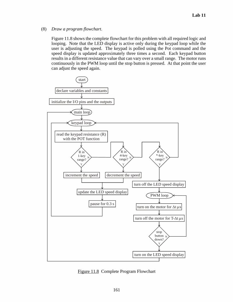
Lab 11
161
(8) Draw a program flowchart.
Figure 11.8 shows the complete flowchart for this problem with all required logic andlooping. Note that the LED display is active only during the keypad loop while theuser is adjusting the speed. The keypad is polled using the Pot command and thespeed display is updated approximately three times a second. Each keypad buttonresults in a different resistance value that can vary over a small range. The motor runscontinuously in the PWM loop until the stop button is pressed. At that point the usercan adjust the speed again.
Figure 11.8 Complete Program Flowchart
Y
N
start
declare variables and constants
initialize the I/O pins and the outputs
main loop
R in4-keyrange?
keypad loop
read the keypad resistance (R)with the POT function
Y
N
R in1-keyrange?
Y
N
R in*-keyrange?
increment the speed decrement the speed
update the LED speed display
pause for 0.3 s
turn off the LED speed display
PWM loop
turn on the LED speed display
turn on the motor for t s
Y
N
stopbuttondown?
turn off the motor for T- t s

Lab 11
162
(9) Write the code.
The PicBasic Pro code ("PWM.bas") corresponding to the flowchart shown in Figure 11.8using the hardware illustrated in Figure 11.5 follows. The code is commented throughout withremarks so it should be self-explanatory. Whenever you write programs, you should alwaysinclude copious remarks so you and others (e.g., co-workers and bosses) can later interpret whatyou have done. Please create this (PWM.bas) and the later file (PWM.cal) before coming toLab so you will have more time to successfully complete the Lab in the allotted time.
NOTE: Be sure to follow the procedure in Section 11.5 and run PWM_cal.bas (shown later)first before loading and running PWM.bas.
' PWM.bas'' Controls the speed of a DC motor using pulse-width modulation (PWM). The speed is adjusted' via user input with three buttons (increase, decrease, and enter) on a numeric keypad. The relative' speed is stored as a number that ranges from 0 (corresponding to 15% duty cycle) to 15' (corresponding to 35% duty cycle). The current value of the speed is displayed graphically' with a set of 4 LEDs that show the bits of the equivalent binary number.
' Identify and set the internal oscillator clock speed (required for the PIC16F88)DEFINE OSC 8OSCCON.4 = 1OSCCON.5 = 1OSCCON.6 = 1
'Turn off the A/D converter (required for the PIC16F88)ANSEL = 0
' Define pin assignments, variables, and constantsled0 Var PORTB.0 ' LSB (bit 0) green LEDled1 Var PORTB.1 ' bit 1 red LEDled2 Var PORTB.2 ' bit 2 red LEDled3 Var PORTB.3 ' MSB (bit 3) red LED
motor Var PORTA.1 ' PWM output pin to motor MOSFET gatechange Var PORTA.3 ' button causing the motor to stop for
' speed adjustmentspeed Var BYTE ' User-input speedMAX_SPEED Con 15 ' Maximum relative speedT Var WORD ' pulse period in millisecondst_on Var WORD ' pulse width (high state)T_t Var WORD ' pulse down (low state) time: (T - t)
pot_pin Var PORTA.2 ' keypad pin for POT commandSCALE Con 255 ' Pot statement scale factorpot_val Var BYTE ' value returned by POT command
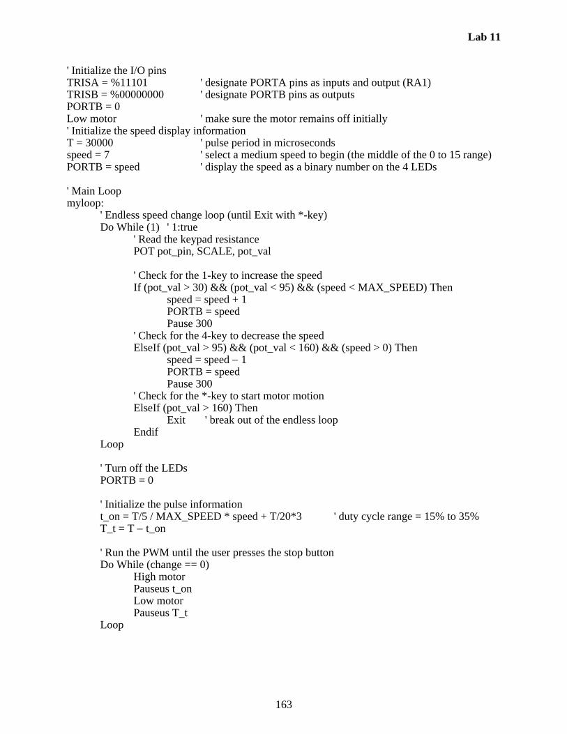
Lab 11
163
' Initialize the I/O pinsTRISA = %11101 ' designate PORTA pins as inputs and output (RA1)TRISB = %00000000 ' designate PORTB pins as outputsPORTB = 0Low motor ' make sure the motor remains off initially' Initialize the speed display informationT = 30000 ' pulse period in microsecondsspeed = 7 ' select a medium speed to begin (the middle of the 0 to 15 range)PORTB = speed ' display the speed as a binary number on the 4 LEDs
' Main Loopmyloop:
' Endless speed change loop (until Exit with *-key)Do While (1) ' 1:true
' Read the keypad resistancePOT pot_pin, SCALE, pot_val
' Check for the 1-key to increase the speedIf (pot_val > 30) && (pot_val < 95) && (speed < MAX_SPEED) Then
speed = speed + 1PORTB = speedPause 300
' Check for the 4-key to decrease the speedElseIf (pot_val > 95) && (pot_val < 160) && (speed > 0) Then
speed = speed 1PORTB = speedPause 300
' Check for the *-key to start motor motion ElseIf (pot_val > 160) Then
Exit ' break out of the endless loopEndif
Loop
' Turn off the LEDsPORTB = 0
' Initialize the pulse informationt_on = T/5 / MAX_SPEED * speed + T/20*3 ' duty cycle range = 15% to 35%T_t = T t_on
' Run the PWM until the user presses the stop buttonDo While (change == 0)
High motorPauseus t_onLow motorPauseus T_t
Loop
Lab 11
164
' Turn the LED speed display back onPORTB = speed
Goto myloop' End of the program (never reached)End
The variable "speed" stores a relative measure of the motor speed as an integer that variesfrom 0 (slow) to 15 (fast). A speed of 0 corresponds to a duty cycle of 15% and the a speed of 15corresponds to a duty cycle of 35%. These duty cycle percentages were determined experimentallyto produce a good range of motor speeds using a 5 V supply. (Note - the motor is rated at only1.5 to 3 V so high duty cycles would result in excessive average voltage, which could damagethe motor.)
One not so obvious challenge in the program is how the variable "t" is calculated. BecausePicBasic Pro stores variables and does arithmetic with limited size integers, you have to be carefulwith truncation and overflow effects when performing calculations. For example, the equation:
t_on = T/5 / MAX_SPEED * speed + T/20*3 (11.3)
would not work properly if it were written as:
t_on = speed / MAX_SPEED * T/5 + T/20*3 (11.4)
or as:t_on = T/5 * speed / MAX_SPEED + T/20*3 (11.5)
The variable speed can vary from 0 to 15, so from Equation 11.3 where MAX_SPEED is 15, t canvary from 3/20 T (15% of T) to 7/20 T (1/5 T + 3/20 T = 35% of T). Note that parentheses are notrequired to have the calculations in the equation execute in the correct order because, as with allprogramming languages, PicBasic Pro gives higher precedence to multiplication and division(which occur from left to right), than with addition and subtraction. Therefore, to PicBasic Pro,Equation 11.3 looks like:
t_on = (((T/5) / MAX_SPEED) * speed) + ((T/20) * 3) (11.6)
There is a problem with Equation 11.4 due to integer arithmetic truncation. Because "speed"varies from 0 to 15 and MAX_SPEED is 15, for all values of speed except 15 (0 through 14), theinteger fraction "speed/MAX_SPEED" will be truncated to 0 (because the result of the division isless than 1) before the remaining calculations are executed. Equation 11.5 will not work as desiredbecause, for high speed values the product "(T/5)*speed" will exceed the largest value that can bestored with a 16-bit WORD variable (216 1 = 65,535). This is called overflow. For all valuesof "speed" greater than 10, the product "(T/5)*speed" will result in overflow, throwing off theremaining calculations. In Equation 11.3, the order of calculations is chosen carefully so notruncation or overflow occurs.
The If statements in the While loop check to determine the range within which the Potcommand variable "pot_val" falls. This allows the program to determine which button on thekeypad is pressed. A separate calibration program is used to determine the appropriate values forthe range limits. This program ("PWM_cal.bas" below) uses the same hardware as for the programabove ("PWM.bas"), but here the LEDs are being used to graphically display the value returned bythe Pot command. The three red LEDs blink individually and sequentially to indicate the number

Lab 11
165
of 100s, 10s, and 1s in the "pot_val" number. The green LED is flashed as a signal between eachred LED’s digit value display. If you had a liquid crystal display (LCD) in your design, it wouldbe a simple matter to display the decimal number on the LCD for easy viewing. However, to usean LCD with the Pic Basic Pro command "Lcdout" requires 7 I/O pins, and many project designswill not have enough spare pins to drive the display. If you only have one or a few output pinsavailable, blinking LEDs offer an alternative method to graphically display the values of numberswithin your running program. In "PWM_cal.bas," since we have four LEDs, we used threedifferent LEDs to indicate the different decimal places for the number. If you didn’t have multipleLEDs in your design or if you only had one pin to spare, you could achieve the same result byblinking a single LED with pauses between each digit number display.
Through testing with the "PWM_cal.bas" program, using a "Pot" command scale value of255, we found the following values for the three keys: 65 for the 1-key, 128 for the 4-key, and 189for the *-key. That is why the following pot_val ranges where used in the "PWM.bas" program:30 to 95 for the 1-key, 95 to 160 for the 4-key, and above 160 for the *-key. The nominal values(65, 128, and 189) fall in the middle of these ranges allowing for small random fluctuations due totemperature and connection resistance changes. Refer to the PicBasic Pro manual for details onhow to select an appropriate value for the "Pot" command scale value. The value 255 is appropriatefor the resistance and capacitance values we selected.
' PWM_cal.bas
' Displays the Pot values for the keypad buttons by blinking the upper three red LEDs. Each' LED is blinked individually to indicate the number of 100s, 10s, and 1s in the' Pot value number. The green LED is flashed once between each blinking red LED display.
' Identify and set the internal oscillator clock speed (required for the PIC16F88)DEFINE OSC 8OSCCON.4 = 1OSCCON.5 = 1OSCCON.6 = 1
' Turn off the A/D converter (required for the PIC16F88)ANSEL = 0
' Define variables, pin assignments, and constantsled0 Var PORTB.0 ' LSB (bit 0) LEDled1 Var PORTB.1 ' bit 1 LEDled2 Var PORTB.2 ' bit 2 LEDled3 Var PORTB.3 ' MSB (bit 3) LEDmotor Var PORTA.1 ' PWM output pin to motor MOSFET gatepot_pin Var PORTA.2 ' keypad pin for POT commandSCALE Con 255 ' Pot statement scale factorpot_val Var BYTE ' value returned by POT commandi Var BYTE ' loop variabledigs Var BYTE ' digit number for each decimal place
' Initialize the I/O pinsTRISA = %11101 ' designate PORTA pins as inputs and output (RA1)

Lab 11
166
TRISB = %00000000 ' designate PORTB pins as outputsPORTB = 0Low motor ' make sure the motor remains off
' User speed change loopenter:
POT pot_pin, SCALE, pot_val
' Flash the LSB green LED and blink each of the upper 3 red LEDs to indicate the number of' 100s, 10s, and 1s in pot_valPORTB = 0
High led0Pause 500Low led0Pause 100digs = pot_val / 100For i = 1 To digs
High led3Pause 300Low led3Pause 300
Next i
pot_val = pot_val - digs*100High led0Pause 500Low led0Pause 100digs = pot_val / 10For i = 1 To digs
High led2Pause 300Low led2Pause 300
Next i
digs = pot_val - digs*10High led0Pause 500Low led0Pause 100For i = 1 To digs
High led1Pause 300Low led1Pause 300
Next iGoto enter

Lab 11
167
' End of program (never reached)End
(10) Build and test the system.
That is your job using the procedure in Section 11.5.
11.4 Troubleshooting and Design Improvements
There are several changes you can make to the circuit to improve the design’s robustness.You will definitely want to explore some of these recommendations if you have troublegetting your circuit to function properly.
If your PIC doesn’t seem to be running properly (e.g., it resets when the motor start buttonis pressed), it might be because the Lab power supply voltage can be affected by current spikes(e.g., the voltage can drop suddenly, causing the PIC to reset). Because the motor is being switchedon and off abruptly, and because the currents in the motor are being switched by the internalcommutator, spikes and noise can occur on the 5V and ground lines. To help minimize theseeffects, you can add capacitance (e.g., 0.1-1.0 F) across the tabs of the motor to help filter outspikes and noise from the commutation. You can also add a 1 F or larger capacitor across the5V and ground line inputs to your breadboard to help stabilize the voltage there. You mightalso try increasing the capacitance between Vdd and ground on the PIC (i.e., replace the 0.1F with 1 F or more). The TA can provide capacitors for testing. Also, make sure the wiresattached to the motor are soldered to the motor tabs to ensure solid and reliable connections. Themotor wires should also be twisted together to limit potential electromagnetic interference (EMI)caused by the wire currents. You should also be careful to limit ground loops in your wiring, andkeep all wires as short as possible (e.g., buy cutting and stripping wires to length) to minimizeEMI. You can also build the circuit on a separate breadboard that has a metal backing, whichadds capacitance to all connect points and helps reduce EMI.
Another alternative is to use separate power sources for the PIC circuit (e.g., the functiongenerator) and the motor (e.g., a Lab power supply, 4 AA batteries in series for 6V, or a 9V batterywith a 5V voltage regulator and 1 F capacitor). This will help limit voltage fluctuations in thePIC circuit when the motor turns on and runs. Using a battery or AC adapter to power the wholesystem (the PIC circuit and the motor) is another alternative. In this case, a capacitor (e.g., 1F ormore) is required across the power and ground lines to help keep the output voltage stable. TheTA will demonstrate the battery-power alternative.
If the motor has a difficult time starting at slow speed with the low-duty-cycle PWM signal,it can help to turn the motor on briefly (e.g., 0.5 s) with a non-PWM constant voltage to help getthe motor starting, before starting the PWM signal. An alternative is to just give the motor a nudgemanually by turning the shaft in the rotation direction.
If you can’t get the Pot command stuff to work properly, an alternative is to wire up thebuttons to separate inputs (with pull-up or pull-down resistors) to read them directly as digitalinputs instead. The TA will demonstrate this alternative.
For other advice and recommendations, see Section 15.5 in Lab 15.

Lab 11
168
11.5 Procedure / Summary Sheet
(1) Complete and attach a detailed functional diagram, using Sections 1.3 and 7.9 in thetextbook for guidance. Submit this on a separate sheet of paper.
(2) Use an ASCII editor (e.g., Windows Notepad or MS Word - Text Only) to create theprogram "PWM_cal.bas" listed in Section 11.3. Save the file in a folder in yournetwork file space.
(3) Follow the procedure in Section 9.4 of Lab 9 to store your program in a PICmicrocontroller that you can insert into your circuit.
(4) Build the circuit shown in Figure 11.5 and insert the PIC programmed with"PWM_cal." You can omit the motor driver circuit for now because it is not used inthe calibration program.
(5) Report the nominal Pot values displayed for your program for each of the activekeypad buttons. Be sure to hold each button down long enough (for 2 green LEDblinks) to start the red LED sequence.
pot_val for the 1-key: 100s: ______ 10s: _______ 1s: ________ value: ______
pot_val for the 4-key: 100s: ______ 10s: _______ 1s: ________ value: ______
pot_val for the *-key: 100s: ______ 10s: _______ 1s: ________ value: ______
(6) Repeat Steps 2 and 3 for the "PWM.bas" program, replacing the "PWM_cal" programon your PIC. Modify the "pot_val" ranges in the PWM.bas "speed change loop"If statements, if necessary based on the values you found in Step 5. Add the motordriver circuit to your board if you haven’t done so already. Insert the reprogrammedPIC into your circuit.
(7) See Section 11.4 if your circuit is assembled correctly but does not workproperly. One thing worth checking is whether or not the motor PWM signal isworking as expected. To do this, disconnect the transistor and look at the PIC outputsignal on the oscilloscope as the speed is changed.
(8) Show your functioning circuit to your TA so he or she can verify it is working.

Lab 11
169
LAB 11 QUESTIONS
Group: ____ Names: _________________________ _____________________________
_________________________ _____________________________
(1) Did your circuit work the first time, without modifications? If not, what things did you tryfrom Section 11.4? Which things worked, and why do you think they worked?
(2) Explain in detail how you think the Pot command works.
(3) In the PWM.bas program, we used 30,000 microseconds for the PWM period. Whatfrequency f (in Hz) does this correspond to?

Lab 11
170
(4) How would the motor respond to a very low (close to 0%) duty cycle PWM signal?
How would changing the PWM signal frequency f (i.e., making it much lower or muchhigher) change the motor response?
(5) What would happen if other keys (besides the 1-key, 4-key, and *-key) are pressed downduring the keypad loop?
What would happen if two of the three valid keys are pressed and held down at once (e.g.,the 1-key and the *-key)?
(6) In PicBasic Pro, to what values would the following expressions evaluate? Hint: PicBasicPro uses integer division and performs one operation at a time.
a) 2 / 3 * 4
b) 2 * 4 / 3
Lab 12
171
Laboratory 12
Data Acquisition
Required Special Equipment:• Computer with LabView Software• National Instruments USB 6009 Data Acquisition Card
12.1 Objectives
This lab demonstrates the basic principals of analog to digital conversion and provides abrief introduction to LabView. A LabView VI file is created which utilizes the USB 6009 DataAcquisition Card to convert an analog signal into a digital signal, store it, and display it. The effectsof sampling frequency will be explored for both a function generator voltage signal and an audiosignal from a stereo amplifier.
12.2 Introduction
A data acquisition system is used to convert an analog signal into a digital signal that canbe stored and processed on a computer. The most common type of analog signal acquired by acomputer is a voltage output from a sensing device. Examples are voltages due to resistancechanges in a strain gage Wheatstone bridge, voltages from an accelerometer charge amplifier, andvoltages from a thermocouple amplifier.
A data acquisition system consists of a sample/hold circuit to capture an instantaneousvalue of a time varying analog voltage signal, an A/D converter to convert this voltage to a digitalcode, and a computer interface that allows storing and processing of the digital data. Thesecomponents are packaged on a PC plug-in board, PCMCIA card, or USB device called a DataAcquisition and Control (DAC) card. These cards support various language programmingenvironments including C, FORTRAN, and BASIC. Various software function calls are providedvia a software library that gives easy high-level access to the board's capabilities. Acquiring datafrom the outside world on the computer is a simple matter of calling a function from a program. ADAC card can also be controlled with LabView, a visual programming interface where icons areselected and connected to achieve the desired functionality. A DAC card can support both inputand output functions including binary (TTL) I/O, analog I/O, and counter/timer features.
12.3 A/D basics
An analog to digital converter converts a continuous analog voltage signal into a discretedigital signal. The digital signal is represented by a certain number of bits (n) and each combinationof bits refers to an output state. Using more bits means that the digital signal can be discretized into
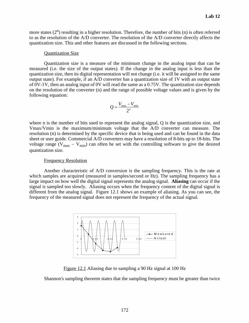
Lab 12
172
more states (2n) resulting in a higher resolution. Therefore, the number of bits (n) is often referredto as the resolution of the A/D converter. The resolution of the A/D converter directly affects thequantization size. This and other features are discussed in the following sections.
Quantization Size
Quantization size is a measure of the minimum change in the analog input that can bemeasured (i.e. the size of the output states). If the change in the analog input is less than thequantization size, then its digital representation will not change (i.e. it will be assigned to the sameoutput state). For example, if an A/D converter has a quantization size of 1V with an output stateof 0V-1V, then an analog input of 0V will read the same as a 0.75V. The quantization size dependson the resolution of the converter (n) and the range of possible voltage values and is given by thefollowing equation:
where n is the number of bits used to represent the analog signal, Q is the quantization size, andVmax/Vmin is the maximum/minimum voltage that the A/D converter can measure. Theresolution (n) is determined by the specific device that is being used and can be found in the datasheet or user guide. Commercial A/D converters may have a resolution of 8-bits up to 18-bits. Thevoltage range (Vmax Vmin) can often be set with the controlling software to give the desiredquantization size.
Frequency Resolution
Another characteristic of A/D conversion is the sampling frequency. This is the rate atwhich samples are acquired (measured in samples/second or Hz). The sampling frequency has alarge impact on how well the digital signal represents the analog signal. Aliasing can occur if thesignal is sampled too slowly. Aliasing occurs when the frequency content of the digital signal isdifferent from the analog signal. Figure 12.1 shows an example of aliasing. As you can see, thefrequency of the measured signal does not represent the frequency of the actual signal.
Figure 12.1 Aliasing due to sampling a 90 Hz signal at 100 Hz
Shannon's sampling theorem states that the sampling frequency must be greater than twice
n
VVQ
2minmax
- 3
- 2
- 1
0
1
2
3
0 0 .0 2 0 .0 4 0 .0 6 0 .0 8
M e a s u re d
A c tu a l
Lab 12
173
the maximum analog frequency to avoid aliasing. This is restated by the following equation.
where fs is the sampling frequency and fmax is the maximum frequency of the analog signal. Thelower bound on the sampling frequency (2fmax) is referred to as the Nyquist frequency. It isimportant to note that the sampling rate must be greater than and not equal to the Nyquist frequencyin order to retain the frequency information of the analog signal. To accurately represent theamplitude variation of the signal within a period of the waveform, the sampling rate must be wellabove the Nyquist frequency.
Amplitude Resolution
Sampling at a rate greater than the Nyquist frequency ensures that the frequency of theanalog signal is represented accurately but does not necessarily ensure that the amplitude of theanalog signal is represented accurately. A criterion for accurately representing the amplitude canbe developed by considering an upper bound on the change in the analog signal between samples.Between samples the analog signal will change by some amount V. By approximating thederivative as constant over this interval the following equation can be used to relate the change inthe signal to the sample time.
where V is the change in the analog signal, Ts is the time between samples, and
is the maximum of the derivative of the analog signal. Since Ts is the time between samples it isthe reciprocal of the sampling frequency (fs). By substituting the sampling frequency, the equationbecomes:
where is determined by the signal and V can be set to influence how finely the
amplitude is represented. A small V means that the sampling frequency will be high and the signalwill be represented well. The maximum derivative is known if the signal is known. If it is not, thena sinusoid can be assumed at the maximum frequency of the signal. The maximum derivative of asinusoid of the form Asin(t) is A. Using this, the previous equation becomes:
where A is the amplitude of the signal and is the maximum frequency. Sampling at fs ensures that
max2 ffs
SMAX
Tdt
tdVV
)(
MAXdt
tdV
)(
Vdt
tdVf
MAXS
1)(
MAXdt
tdV
)(
V
AfS

Lab 12
174
the signal will not change more than V between samples. How accurately the amplitude isrepresented can therefore be controlled by selecting V. It is important to remember that due to theapproximations made above, V is an upper bound and the signal will change less than V. Also,using a very small V will lead to a very fast sampling rate that may not be possible with someconverters, and fast sampling will result in large amounts of data which can be an issue when usingdevices with limited memory like microcontrollers. V should be chosen to be the largest valuethat gives adequate results meaning that the sampling frequency is the smallest possible that givesadequate results.
12.4 Introduction to LabView programming
LabView is a graphical programming environment with an intuitive user interface. It hasmany built-in features for data acquisition and works well with many commercial DAC cards. Avery brief description of LabView is presented below.
There are two primary windows in LabView, the Block Diagram and Front Panel window(see Figures 12.2 and 12.3). Ctrl-T can be used to switch between the windows. The BlockDiagram window contains the graphical program that you create, and the Front Panel windowcontains the user interface. The user interface is used to input control parameters, run the program,and visualize the results (e.g. plot of a waveform).
Additional windows called palettes contain the libraries of built-in LabView functions andare used to set the function of the cursor. The Functions palette is a library of blocks that can beused in the Block Diagram window (it is only available when the Block Diagram window isactive). The Controls palette is a library of the functions available for the front panel (it is onlyavailable when the Front Panel window is active). The Tools palette sets the function of the cursor.
Different tools are used to perform different functions. For example, connect wire is used
to connect blocks, and operate value is used to change the value of a control (described
below). Alternatively, the automatic tool selection will automatically change which
tool you are using depending on the location of the cursor.
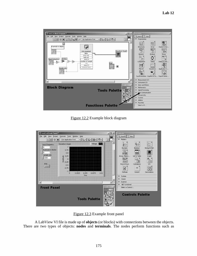
Lab 12
175
Figure 12.2 Example block diagram
Figure 12.3 Example front panel
A LabView VI file is made up of objects (or blocks) with connections between the objects.There are two types of objects: nodes and terminals. The nodes perform functions such as
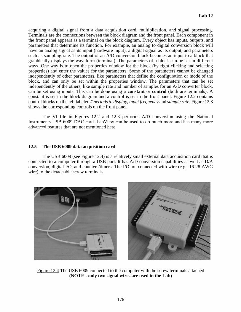
Lab 12
176
acquiring a digital signal from a data acquisition card, multiplication, and signal processing.Terminals are the connections between the block diagram and the front panel. Each component inthe front panel appears as a terminal on the block diagram. Every object has inputs, outputs, andparameters that determine its function. For example, an analog to digital conversion block willhave an analog signal as its input (hardware input), a digital signal as its output, and parameterssuch as sampling rate. The output of an A/D conversion block becomes an input to a block thatgraphically displays the waveform (terminal). The parameters of a block can be set in differentways. One way is to open the properties window for the block (by right-clicking and selectingproperties) and enter the values for the parameters. Some of the parameters cannot be changedindependently of other parameters, like parameters that define the configuration or mode of theblock, and can only be set within the properties window. The parameters that can be setindependently of the others, like sample rate and number of samples for an A/D converter block,can be set using inputs. This can be done using a constant or control (both are terminals). Aconstant is set in the block diagram and a control is set in the front panel. Figure 12.2 containscontrol blocks on the left labeled # periods to display, input frequency and sample rate. Figure 12.3shows the corresponding controls on the front panel.
The VI file in Figures 12.2 and 12.3 performs A/D conversion using the NationalInstruments USB 6009 DAC card. LabView can be used to do much more and has many moreadvanced features that are not mentioned here.
12.5 The USB 6009 data acquisition card
The USB 6009 (see Figure 12.4) is a relatively small external data acquisition card that isconnected to a computer through a USB port. It has A/D conversion capabilities as well as D/Aconversion, digital I/O, and counters/timers. The I/O are connected with wire (e.g., 16-28 AWGwire) to the detachable screw terminals.
Figure 12.4 The USB 6009 connected to the computer with the screw terminals attached(NOTE - only two signal wires are used in the Lab)

Lab 12
177
Terminals 1-16 are used for analog I/O, and terminals 17-32 are used for digital I/O andcounter/timer functions (see Figure 12.5). Notice that the analog terminals are different dependingon which mode the device is in, single-ended mode (also known as reference-signal-ended or RSE)or differential mode. In single-ended mode the positive voltage signal is connected to an AIterminal and the negative voltage signal is connected to a GND terminal. This mode uses twoterminals allowing eight analog inputs (AI0-AI7). The maximum voltage range in this mode is-10V to 10V. Differential mode can be used to obtain a larger voltage range. This mode measuresthe difference between two signals, AI+ and AI-; each referenced to GND. A voltage range of -20V to 20V can be achieved, but the maximum voltage on one pin (AI+ or AI-) referenced toground is ±10V. This means the 20V amplitude sine wave cannot be measured using a single pin(AI+ or AI-). A combination of two 10V amplitude sine waves that are 180 degrees out of phasewould need to be applied to AI+ and AI-. Differential mode uses one more wire than single-endedmode, so only four analog inputs are available. A description of each signal is summarized inFigure 12.6.
Figure 12.5 Analog (1-16) and Digital (17-32) pin assignments of the USB 6009
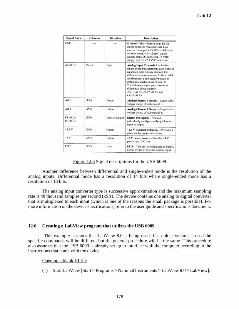
Lab 12
178
Figure 12.6 Signal descriptions for the USB 6009
Another difference between differential and single-ended mode is the resolution of theanalog inputs. Differential mode has a resolution of 14 bits where single-ended mode has aresolution of 13 bits.
The analog input converter type is successive approximation and the maximum samplingrate is 48 thousand samples per second (kS/s). The device contains one analog to digital converterthat is multiplexed to each input (which is one of the reasons the small package is possible). Formore information on the device specifications, refer to the user guide and specifications document.
12.6 Creating a LabView program that utilizes the USB 6009
This example assumes that LabView 8.0 is being used. If an older version is used thespecific commands will be different but the general procedure will be the same. This procedurealso assumes that the USB 6009 is already set up to interface with the computer according to theinstructions that come with the device.
Opening a blank VI file
(1) Start LabView [Start > Programs > National Instruments > LabView 8.0 > LabView].
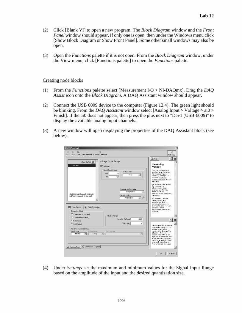
Lab 12
179
(2) Click [Blank VI] to open a new program. The Block Diagram window and the FrontPanel window should appear. If only one is open, then under the Windows menu click[Show Block Diagram or Show Front Panel]. Some other small windows may also beopen.
(3) Open the Functions palette if it is not open. From the Block Diagram window, underthe View menu, click [Functions palette] to open the Functions palette.
Creating node blocks
(1) From the Functions palette select [Measurement I/O > NI-DAQmx]. Drag the DAQAssist icon onto the Block Diagram. A DAQ Assistant window should appear.
(2) Connect the USB 6009 device to the computer (Figure 12.4). The green light shouldbe blinking. From the DAQ Assistant window select [Analog Input > Voltage > ai0 >Finish]. If the ai0 does not appear, then press the plus next to "Dev1 (USB-6009)" todisplay the available analog input channels.
(3) A new window will open displaying the properties of the DAQ Assistant block (seebelow).
(4) Under Settings set the maximum and minimum values for the Signal Input Rangebased on the amplitude of the input and the desired quantization size.

Lab 12
180
(5) Under Settings set the Terminal Configuration to RSE (single-ended mode).
(6) Under the Task Timing tab set the acquisition mode to N samples. The wiring diagramcan be viewed by selecting the Connection Diagram tab towards the bottom of thewindow assuming an appropriate range was selected (see step 1 in the Lab Procedureto follow).
(7) Select [Ok] to close the DAQ Assistant properties window. This may be opened laterby right-clicking on the DAQ Assistant block.
Creating terminal blocks
(1) Select the spool of wire icon from the Tools palette (accessible under the View
menu). Right-click on the rate input (arrow on the side of the block) on the DAQAssistant block and select [create > control]. A block labeled rate should appear witha wire connected to the DAQ Assistant block.
(2) Repeat this to create a control for the number of samples input. These two controlswill appear in the Front Panel window.
(3) Activate the Front Panel window and open the controls palette if it is not open. Fromthe Front Panel window under the View menu, select Controls Palette to open theControls palette.
(4) From the Controls palette select [modern > graph] and drag the Waveform Graph icononto the Front Panel window. A block labeled Waveform graph will appear in theBlock Diagram window.
(5) Right-click on the graph and select [properties]. Under the Scales tab select[Amplitude (Y-axis)] in the top pull-down menu. Deselect Autoscale and set themaximum and minimum to the values used for the signal input range on the DAQAssistant block. Click [OK] to close the properties window.
(6) Select the Block Diagram window and select the wire spool icon (or automatic
icon) on the Tools palette. Click on the data output of the DAQ Assistant block andon the Waveform Graph block. A wire will now connect the two blocks.
Running the program
(1) Connect the analog signal to the USB 6009. The positive voltage signal is connectedto screw terminal 2 (AI0) and the negative voltage signal is connected to screwterminal 1 (GND).

Lab 12
181
(2) Select the Front Panel window and select the operate value icon from the
Tools palette (or automatic icon).
(3) Set the rate and number of samples controls to appropriate values.
(4) Under the Operate menu select [run] to run the program (or use the large right-arrowon the toolbar under the menu bar). A waveform should appear on the WaveformGraph. A picture of the waveform can be saved to a file by right-clicking on thewaveform and selecting [Data Operations > Export Simplified Image…].

Lab 12
182

Lab 12
183
12.7 Laboratory Procedure / Summary Sheet
Group:_______ Names:_______________________________________________
(1) Calculate the maximum allowable voltage range resulting in a measurement accuracy(quantization size) of 1 mV. The resolution of the USB 6009 is 13 bits in the modethat we will be using.
Vmax Vmin = _____________V (round down)
Select a maximum and minimum voltage to be used in the LabView program if a2sin(200t) V signal is to be measured.
Vmax = _____________V Vmin = _____________V
(2) For the following input signal 2sin(200t)V, what is the Nyquist frequency? What isthe sampling frequency that ensures the signal changes less than 0.4V (1/10 of Vp-p)between samples?
Nyquist frequency = _______________Hz fS = _________________Hz
Fill out the following table to display 4 periods of the analog signal. Round up andremember to account for the starting sample (i.e. add 1).
(3) Follow the procedure from Section 12.6 to create a LabView VI file.
(4) Use a function generator to create the analog 2sin(200t) and connect the output tothe USB 6009. Use the values from parts (1) and (2) as parameters in the LabViewprogram and sketch the resulting waveforms on separate paper.
(5) In this portion of the lab you will sample music at different sampling rates and listento the resulting waveform.
Sampling Rate (Hz)Number of
Samples
90
150
175
200
500
1000
2000
3000
4000
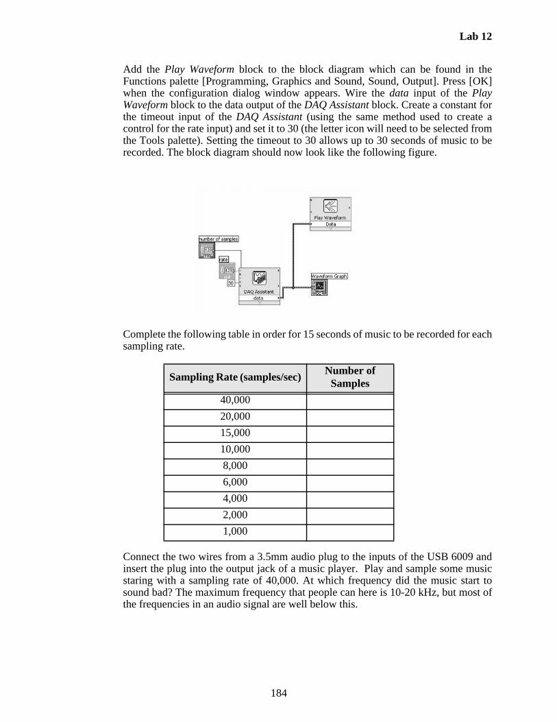
Lab 12
184
Add the Play Waveform block to the block diagram which can be found in theFunctions palette [Programming, Graphics and Sound, Sound, Output]. Press [OK]when the configuration dialog window appears. Wire the data input of the PlayWaveform block to the data output of the DAQ Assistant block. Create a constant forthe timeout input of the DAQ Assistant (using the same method used to create acontrol for the rate input) and set it to 30 (the letter icon will need to be selected fromthe Tools palette). Setting the timeout to 30 allows up to 30 seconds of music to berecorded. The block diagram should now look like the following figure.
Complete the following table in order for 15 seconds of music to be recorded for eachsampling rate.
Connect the two wires from a 3.5mm audio plug to the inputs of the USB 6009 andinsert the plug into the output jack of a music player. Play and sample some musicstaring with a sampling rate of 40,000. At which frequency did the music start tosound bad? The maximum frequency that people can here is 10-20 kHz, but most ofthe frequencies in an audio signal are well below this.
Sampling Rate (samples/sec)Number of
Samples
40,000
20,000
15,000
10,000
8,000
6,000
4,000
2,000
1,000

Lab 12
185
LAB 12 QUESTIONS
Group:_____ Names:__________________________________________________
(1) For part (2) at what frequencies did you see aliasing?
(2) For part (1), what would the voltage range need to be to get a quantization size lessthan 0.2mV? Is it possible to measure 2sin(200t) at this quantization size?
(3) What resolution A/D converter should be used to measure a signal that can rangebetween -8V to 8V with an accuracy of 10mV?
(4) To measure the signal 2sin(200t), draw a wiring diagram showing how you wouldconnect the function generator to the USB 6009 in Differential Mode.
(5) With the USB 6009 in Differential Mode, what two signals would need to beconnected to AI+ and AI- to give a 15sin(2t) waveform? (Hint: see Section 12.5.)

Lab 12
186
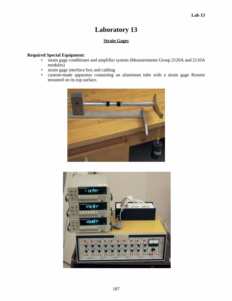
Lab 13
187
Laboratory 13
Strain Gages
Required Special Equipment:• strain gage conditioner and amplifier system (Measurements Group 2120A and 2110A
modules)• strain gage interface box and cabling• custom-made apparatus containing an aluminum tube with a strain gage Rosette
mounted on its top surface.
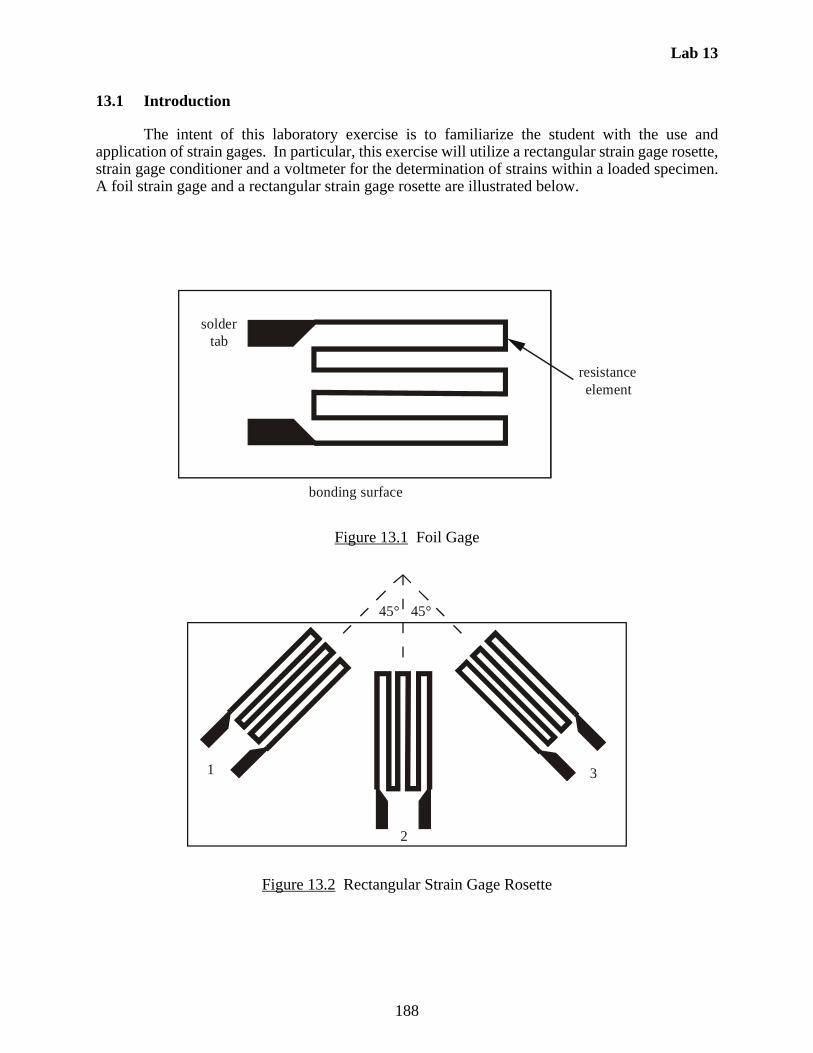
Lab 13
188
13.1 Introduction
The intent of this laboratory exercise is to familiarize the student with the use andapplication of strain gages. In particular, this exercise will utilize a rectangular strain gage rosette,strain gage conditioner and a voltmeter for the determination of strains within a loaded specimen.A foil strain gage and a rectangular strain gage rosette are illustrated below.
Figure 13.1 Foil Gage
Figure 13.2 Rectangular Strain Gage Rosette
solder tab
resistance element
bonding surface
1
2
3
45° 45°

Lab 13
189
13.2 Theory
The basic principle under which the strain gage operates is the fact that the electricalresistance of a conductor changes in response to a mechanical deformation:
(13.1)
where
R = resistance of conductor
= resistivity of material
L = length of conductor
A = cross-sectional area of conductor
Relating the above definition to Poisson's ratio and strain yields the following:
(13.2)
(13.3)
where
F = gage factor
= Poisson's ratio
= axial strain
R = change in gage resistance due to deformation
R = undeformed gage resistance
The strain gage conditioner consists of several channels, each containing a bridge/amplifiercircuit. Each channel outputs a bridge detector potential, Vo, that is related to the strain in the gageconnected to that channel. A bridge circuit is illustrated in Figure 13.3. For a balanced bridge (i.e.,Vo = 0) the condition R1R3 = R2R4 must be satisfied. Thus, once the bridge is balanced for a nostrain condition, a strain induced on the strain gage will result in a nonzero detector potential Vo.The change in this voltage can then be used to determine the corresponding strain. When the gage
R LA----=
F 1 2 1---
-------+ +=
1F---R
R--------=
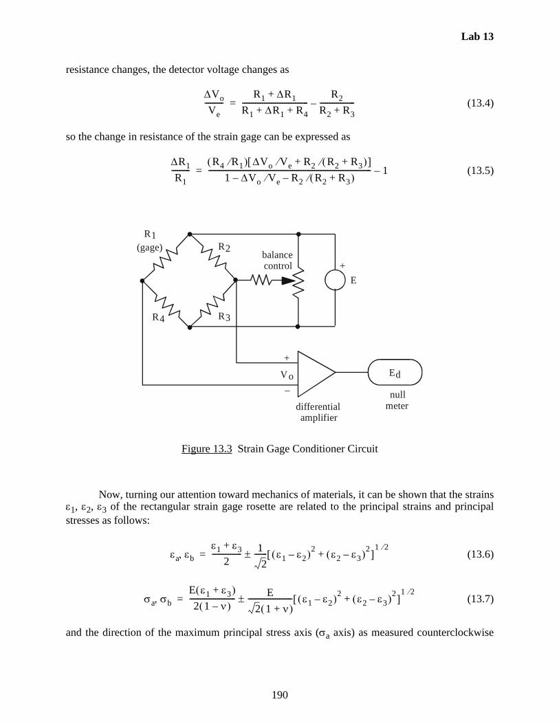
Lab 13
190
resistance changes, the detector voltage changes as
(13.4)
so the change in resistance of the strain gage can be expressed as
(13.5)
Figure 13.3 Strain Gage Conditioner Circuit
Now, turning our attention toward mechanics of materials, it can be shown that the strains1, 2, 3 of the rectangular strain gage rosette are related to the principal strains and principalstresses as follows:
(13.6)
(13.7)
and the direction of the maximum principal stress axis (a axis) as measured counterclockwise
Vo
Ve----------
R1 R1+
R1 R1 R4+ +------------------------------------
R2
R2 R3+-------------------–=
R1
R1----------
R4 R1 Vo Ve R2 R2 R3+ + 1 Vo Ve– R2 R2 R3+ –
----------------------------------------------------------------------------------------- 1–=
+
R1 (gage)
R4 R3
R2balance control
differential amplifier
null meter
+
–
Vo
E
Ed
a b1 3+
2---------------- 1
2------- 1 2– 2 2 3– 2+
1 2=
a bE 1 3+ 2 1 –
------------------------- E
2 1 + ------------------------ 1 2– 2 2 3– 2+
1 2=

Lab 13
191
from gage 1 is given by:
(13.8)
and since 2 > 0.5 (1+3), we use solution in the top half plane (0 < 2 < 180°).
The rectangular strain gage rosette senses the state of strain at a point on the top of thetubular cantilever beam. The stress due to bending at this point is:
(13.9)
and the shear stress is:
(13.10)
where
M = moment corresponding to applied load
T = torque corresponding to applied load
c = radius to outer surface of the tube
I = area moment of inertia of the tube
J = polar area moment of inertia of the tube
x = axial direction
The moment of inertia and polar moment of inertia for a tube are:
(13.11)
(13.12)
Since the shear stress on the principal planes is zero, and since x is located at an angle
= 45° – (13.13)
2tan22 1– 3–
1 3–------------------------------=
xMc
I--------=
xyTcJ
------=
I64------ do
4di
4– =
J 2I32------ do
4di
4– = =

Lab 13
192
from the principal axes (from Mohr’s Circle), the plane stress equations give us:
(13.14)
(13.15)
where avg = 0.5 (a + b).
x avg
a b–
2----------------- 2cos+=
xy
a b–
2----------------- 2sin=

Lab 13
193
13.3 Laboratory Procedure / Summary Sheet
Group: ____ Names: _________________________ _____________________________
_________________________ _____________________________
The experimental setup is illustrated in Figure 13.4. We wish to determine the bendingmoment M (theoretical value = mgb), the torque T (theoretical value = mga), and the mass m byutilizing the strain gage measurements given.
Properties and geometry of the aluminum tube, strain gage rosette, and hanging mass:
E = 70 GPa, = 0.334L = 0.395 m, a = 0.16 m, b = 0.182 mdo = 1.00 in, t = 0.085 inF = 2.05m = 1.492 kg
Figure 13.4 Experimental Setup
L
mg
a
x
Rossette
b

Lab 13
194
(1) It can be shown (see "Experimental Stress Analysis" by Dally and Riley, McGraw-Hill,1991) that an active gage (with gage factor F) produces approximately F/4 output
microvolts per microstrain and per volt excitation. NOTE - this is a unitless quantity: .
Thus the equation relating strain to measured voltage is:
(13.16)
For an excitation potential of 5 volts, we wish to find the gain of the amplifier required toproduce a 2 volt output at 500. Calculate the required gain assuming a gage factor of 2,realizing that the gage factors for the gages being used might be different.
Gain = ______________
(2) The strain gage rosette is connected to channels 1, 2 and 3 on the 2120A. Make sure thatthe gain multiplier control is set to x200. Now set the gain control dial based on the valuecalculated in part 1; i.e. set the gain control to gain/200 for channels 1 – 3.
(3) Make sure that there is no external load applied to the cantilever. Now adjust the bridgebalance for each channel (1 – 3); First turn the EXCIT toggle ON and rotate the BALANCEcontrol until both output lamps are extinguished. If the (-) lamp is illuminated turn theBALANCE control clockwise. Conversely, if the (+) lamp is illuminated turn theBALANCE control counterclockwise. If you are having difficulty distinguishing whetheror not the lamps are illuminated, you may use a voltmeter attached to the DAC interfacecard to zero the bridge potential. Under no load conditions each channel should read zerovolts; adjust the BALANCE control accordingly.
(4) Hang the mass from the center of the tube and record the gage voltages. Comment on theseresults.
(5) Hang the mass at the end of the lever arm. Using a voltmeter, read the voltagescorresponding to gages 1, 2 and 3, and record them below. Also, be sure to measure theactual excitation voltage on each bridge using the selector knob and ports on the right sideof the bridge unit.
V1 = ______________ V1ext = ______________
V2 = ______________ V2ext = ______________
V3 = ______________ V3ext = ______________
VV-----------
Vmeas GAIN
F4--- Vex
----------------------------------=

Lab 13
195
(6) Now calculate the strains in each of the three gages of the rosette; utilize the relationshipfrom part 1.
1 = ______________
2 = ______________
3 = ______________
(7) Knowing these strains determine the following:
a) The bending moment in the beam associated with the applied load.
b) The torque produced by the lever arm and the applied load.
c) The mass applied at the end of the lever arm.
(8) Submit your full analysis used to determine the value of the hung mass from the strain gagevoltage measurements. Compare the calculated result to the actual value of the mass.Submit your work to your TA at the following week’s Lab meeting. Comment on variouspossible sources for error in the measurements and analyses.

Lab 13
196

Lab 14
197
Laboratory 14
Vibration Measurement With an Accelerometer
Required Special Equipment:• custom-made apparatus consisting of two sets of motors/shafts/bearings mounted on an
aluminum plate• Endevco 2721B charge amp• Endevco 2256M15 or 2211E accelerometer• high current power supply (HP 6286A)
14.1 Objective
The objective of this exercise will be to compare the vibration characteristics of a normaland a defective ball bearing turning under load. The vibrations will be sensed with twopiezoelectric accelerometers. The oscilloscope spectrum analyzer will be used to comparevibrations from the two bearings to detect defects.
14.2 Background
Vibration Measurement With Piezoelectric Crystals
Piezoelectric accelerometers are in wide use for measuring shock and vibration. Mostaccelerometers have a design similar to that illustrated in Figure 14.1. The mass (called the seismicmass) causes inertial loads in response to motion of the object to which the accelerometer isattached. The inertial loads cause strain of the piezoelectric crystal. Due to the piezoelectricproperties of the crystal, the strain causes displacement charge which is sensed at the crystalconductive coatings. A charge amplifier and conditioning circuit can measure this charge andconvert it to a voltage signal which represents the acceleration of the object. A pre-loaded springis used to keep the crystal in compression resulting in more linear behavior of the crystal.
In general, piezoelectric accelerometers cannot measure constant or slowly changingacceleration since the crystals can only measure a change in force by sensing a change in strain.But they are excellent for dynamic measurements such as vibration and impacts.
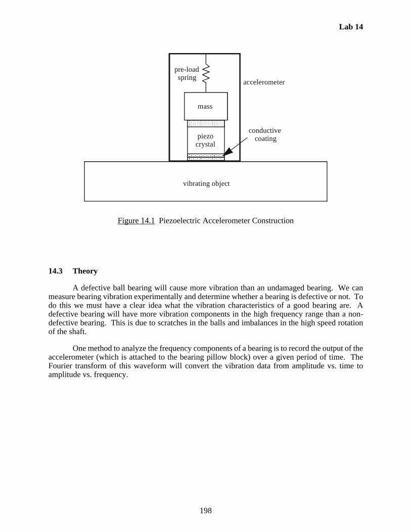
Lab 14
198
Figure 14.1 Piezoelectric Accelerometer Construction
14.3 Theory
A defective ball bearing will cause more vibration than an undamaged bearing. We canmeasure bearing vibration experimentally and determine whether a bearing is defective or not. Todo this we must have a clear idea what the vibration characteristics of a good bearing are. Adefective bearing will have more vibration components in the high frequency range than a non-defective bearing. This is due to scratches in the balls and imbalances in the high speed rotationof the shaft.
One method to analyze the frequency components of a bearing is to record the output of theaccelerometer (which is attached to the bearing pillow block) over a given period of time. TheFourier transform of this waveform will convert the vibration data from amplitude vs. time toamplitude vs. frequency.
pre-load spring
mass
piezo crystal
conductive coating
accelerometer
vibrating object
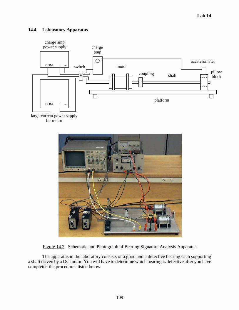
Lab 14
199
14.4 Laboratory Apparatus
Figure 14.2 Schematic and Photograph of Bearing Signature Analysis Apparatus
The apparatus in the laboratory consists of a good and a defective bearing each supportinga shaft driven by a DC motor. You will have to determine which bearing is defective after you havecompleted the procedures listed below.
large-current power supplyfor motor
charge amp power supply charge
amp
motor
coupling
accelerometer
pillow blockshaft
platform
COM + –
COM + –
switch

Lab 14
200
The accelerometers are mounted on plexiglass blocks which are in turn rigidly attached tothe bearing pillow block. The acclerometers are connected to charge amplifiers.
Only one motor should be operated at a time in order to prevent cross-talk of vibrationbetween the two bearings. The supply of the corresponding charge amplifier is selected with thehelp of the toggle switch.
A strobe light can be used to measure the shaft speed. By drawing an axial line on one sideof the shaft and a transverse line on the other side, you can attain a reliable strobe lightmeasurement. If the strobe is set to the shaft speed, one of the lines will be illuminated on eachrotation of the shaft resulting in a stationary line image. If the strobe speed is set to half of the shaftspeed, one of the lines will be illuminated on every second rotation of the shaft resulting in adimmer image. If the strobe speed is set to twice the shaft speed, each line will be alternatelyilluminated on every half turn of the shaft resulting in a plus sign image. There are many morepossibilities depending upon the shaft and strobe speeds, but a reliable method to acquire a goodmeasurement is to start with a high strobe speed and decrease the speed until the image changesfrom a relatively bright stationary plus sign image to a bright single line stationary image.
As an alternative to the strobe light, you may use the reflective tape on the shaft and aretroreflective photosensor. The pulse train coming from the photosensor can be displayed on anoscilloscope and used to measure the frequency of revolution and thus the revolutions per second(rps) of the shaft.

Lab 14
201
14.5 Laboratory Procedure / Summary Sheet
Group: ____ Names: _________________________ _____________________________
_________________________ _____________________________
(1) Select the motor/bearing you want to take data from and set the toggle switch to thecorrect position.
(2) Switch on the power supplies for the charge amplifier and the motors.
(3) Set the motor speed to 3600 rpm with the aid of the strobe or retroreflectivephotosensor.
(4) Look at the waveform you are getting on the oscilloscope.
(5) Process the waveform using the Fast Fourier Transform (FFT) feature on theoscilloscope. To access this feature on an HP Digital oscilloscope, use the ± buttonbetween the channel 1 and channel 2 buttons to access a menu that allows you toperform math on the signals. Turn on Function 2 and display the FFT menu (NOTE:this feature is available only on the HP54602A oscilloscopes equipped with theHP54657A Measurement/Storage module). Turn off the channel 1 and 2 displays(with the Channel buttons) so only Function 2 is on. This results in a clear linespectrum display. Sketch the vibration waveform and the FFT spectrum.Alternatively, acquire the data with LabView and the DAC hardware, and process itin MATLAB, MathCAD, or LabView to generate FFT spectrum plots.
(6) Repeat the procedure for the other motor/bearing.
Compare the two sets of waveforms and spectrum plots. Try to draw conclusions aboutwhich bearing is in better shape. Submit the sketches and comments to the TA.

Lab 14
202

Lab 15
203
Laboratory 15
Practical Advice for Microcontroller-based Design Projects
The project for the course is described in detail on the course website. Here is the directlink:
www.engr.colostate.edu/~dga/mech307/project.html
The purpose for this "laboratory" is to summarize many useful practical resources, considerations,and suggestions that might be helpful to you in designing and implementing your project. Pleaseread this material and apply the suggestions in your design.
15.1 dc Power Supply Options for PIC Projects
There are a number of ways to provide the dc power required by the PIC and any ancillarydigital integrated circuits. Actuators may also be powered by the same dc supply if their drivevoltage match that of the digital circuitry, and if the current demands do not exceed the supply'scapacity. We begin by assuming that TTL digital ICs are used in the project, requiring a closelyregulated 5V dc source. If CMOS is used exclusively, there are fewer restrictions on the regulationof the dc voltage.
Figure 15.1 shows various low cost options for powering systems requiring a 5V supply.The options include:
(1) a 6 V, 9 V, or 12 V wall transformer with a 5 V regulator
(2) a potted power supply with ac input and 5 V regulated output
(3) four AA batteries (6 V) in series with a 5 V regulator
(4) a 9 V battery with a 5 V regulator
(5) a rechargeable battery (or batteries in series) with a 5V regulator
(6) a full featured instrumentation power supply
Other alternatives for powering projects include a computer power supply, or large batteries (e.g.,car or motorcycle lead-acid batteries), especially if you have high current demands.
Lab 15
204
Figure 15.1 Low Cost Power Supply Options
A wall transformer (6 V, 9 V, or 12 V) will provide current at its rating, and must be usedwith a 5V regulator to control the level of the output voltage. Be sure that the current rating of thewall transformer exceeds the maximum current your circuit and actuators will draw. A pottedpower supply also has ac inputs and may provide one or more regulated dc outputs at its ratedcurrent. No voltage regulator is required if a 5V output is provided. Four AA batteries may beconnected in series with the 6 V output regulated down to 5 V with a voltage regulator. A 9 Vbattery must also be connected to a 5 V regulator.
Battery power supply options provide portability for your design but may not be able tosupply enough current. Section 15.2 presents more information on different types of batteries andtheir characteristics. Generally, actuators such as motors and solenoids as well as LED’s can drawsubstantial current, and batteries should be tested before assuming that they will provide sufficientcurrent. Digital circuitry, on the other hand, usually draws very little current.
Figure 15.2 shows an example of a full-featured instrumentation power supply. Thisparticular model (HP 6235A) is a triple-output power supply, with 3 adjustable voltage outputs,each independently current rated. A full featured instrumentation power supply provides theeasiest solution, but is expensive, heavy, and generally is not portable.
wall transformerpotted
power supply4 AA batteries
in series9V battery
voltage regulator
Lab 15
205
Figure 15.2 An Example of a Full-featured Instrumentation Power Supply
Except for the 5V potted supply and the adjustable instrumentation power supply, voltageregulators are required to convert the output voltage down to the 5V level. If your system isentirely CMOS, the regulation of the dc voltage is not required. Figure 15.3 illustrates a standard7805 5V voltage regulator and shows how it is properly connected to your unregulated powersupply output and your system. There must be a common ground from the power supply to yoursystem. The mounting hole allows you to easily attach a heat sink to heat dissipate heat whennecessary.
Figure 15.3 7805 Voltage Regulator Connections
heat sink(COMMON)
INPUT OUTPUT
COMMON
mountinghole
input(7V - 35V)
output(5V regulated)
ground

Lab 15
206
When using a voltage regulator, one needs to be aware that if the voltage drop is large fromthe input to the output, and if significant current is drawn, the regulator will consume significantpower and get very hot. A heat sink (and maybe a fan blowing on the heat sink) might be requiredto help dissipate this heat. If the voltage regulator gets too hot, it can be damaged. An alternativeto dealing with the heat is to use a voltage source (or sources) better matched to the project needs,so the voltage regulator doesn’t need to drop the voltage as much. Another good approach is to usedifferent voltage sources for different voltage requirements. For example, use a source close to 5Vto power your digital circuits, and use a different and dedicated source (and voltage regulator ifnecessary) to power devices (e.g., motors) that require different voltage levels. Another option isto use a voltage regulator or dc-to-dc converter that can drop the voltage more efficiently (e.g., a“switching” type instead of a “linear” type).
Table 15.1 provides a summary of how the various power supply options compare in termsof current ratings, size, and cost. Figure 15.4 shows an example specification sheet for an enclosedpower supply. Before selecting or purchasing a supply for your design, it is important to firstreview the specifications, especially the current rating (2.5 A in this case).
Table 15.1 5V Power Supply Options Summary
Device Typical current Relative size Relative cost
instrumentation power supply 1 A – 5 A large very expensive (~$1000)but many features
small potted, open frame,or enclosed power supply
1 A – 10 A medium moderately expensive(~$20-$100)
wall transformer 1 A small cheap
9V battery 100 mA small cheap
4 AA batteries 100 mA small cheap
rechargeable battery See Section 15.2 small moderate

Lab 15
207
Figure 15.4 Specifications for an Example Closed Frame Power Supply
Lab 15
208
15.2 Battery Characteristics
Many mechatronic designs will require dc voltage sources of some sort, usually tightlyregulated, and often with high current capacities if actuators such as dc motors or solenoids areused. Here we present some of the important terms, considerations, and specifications in the properselection of a battery as a power source.
The most important specification for a battery (besides its rated voltage) is the amp-hourcapacity. It is defined as the current a battery can provide for one hour before it reaches its end-of-life point. The current that a battery can deliver is limited by its equivalent series resistance,which is the internal resistance that is in series with the “ideal voltage source” that is inside thebattery. Batteries are composed of cells, the electro-chemical device that supplies the voltage andcurrent. Cells may be combined in series or parallel within a battery for larger current and voltagecapacities. The voltage of a cell will differ among the types of batteries due to their chemistry.
Primary cells are not rechargeable and are meant for one-time-use. Devices that are usedinfrequently or that require very low drain currents are good candidates for primary cells.Secondary cells are rechargeable, and their effectiveness may be replenished many times. Devicesthat require daily use with higher drain currents are good candidates for secondary cells.
The plot of the battery discharge curve is important in determining the stability of thevoltage output. Figure 15.5 shows a typical shape for a discharge curve. One desires a broadplateau characteristic for the curve.
Figure 15.5 Example Battery Discharge Curve
The maximum current that a battery can deliver depends on the internal resistance of thebattery. The load current times the internal resistance will result in a voltage drop reducing theeffective voltage of the battery. Furthermore, there will be power dissipated by the internalresistance that, at high currents, may result in considerable heat production.
The salient factors a designer must consider in the selection of a power source for amechatronic design are:
o voltage required by the loado current required by the load
Cell Voltage mid-point voltage
end of life voltage
Time

Lab 15
209
o duty cycle of the systemo costo size and weight (specific energy)o need for rechargeability
As shown in Table 15.2, the chemistry of the cell will determine its open circuit voltage.High drain rate devices are good candidates for lead-acid and NiCd batteries. If a device is instorage most of the time, alkaline batteries are appropriate. Since batteries may be the heaviestcomponent of a mechatronic design, the very light Li-ion and lithium-polymer chemistries may begood candidates. Lithium chemistries provide the highest energy per unit weight (specific energy)and per volume (energy density) of all types of batteries.
Rechargeable batteries will function well even after hundreds of cycles. Rechargeablebatteries are significantly more expensive than primary cell batteries. Ni-MH batteries should bedeep discharged several times when put into service for best performance. Ni-Cd batteries cansuffer from an effect called "memory" where the battery capacity can diminish over time. It iscaused by shallow charge cycles where the battery is only partially discharged and then fullycharged repeatedly. You should give the battery a deep discharge from time to time for bestperformance.
Lab 15
210
Table 15.2 Characteristics for Various Types of Batteries
Type Voltage(open
circuit)
Type Typical Ah Capacity
R internal
()
9V (heavy duty) 9 V primary 0.30 @ 1 mA0.15 @ 10 mA
35
9V alkaline 9 V primary 0.60 @ 25 mA 2
9V lithium 9 V primary 1.0 @ 25 mA0.95 @ 80 mA
18
alkaline D 1.5 V primary 17.1 @ 25 mA 0.1
alkaline C 1.5 V primary 7.9 @ 25 mA 0.2
alkaline AA 1.5 V primary 2.7 @ 25 mA 0.4
alkaline AAA 1.5 V primary 1.2 @ 25 mA 0.6
BR-C PCMF-Li 3 V primary 5.0 @ 5 mA
CR-V3 Mn-Li 3 V primary 3.0 @ 100 mA
Ni-Cd D 1.3 V secondary 4.0 @ 800 mA3.5 @ 4 A
0.009
Ni-Cd 9V 8.1 V secondary 0.1 @ 10 mA 0.84
Lead-acid D 2.0 V secondary 2.5 @ 25 mA2.0 @ 1 A
0.006
Ni-MH AAA 1.2 V secondary 0.55 @ 200 mA
Ni-MH AA 1.2 V secondary 1.3 @ 200 mA
Ni-MH C 1.2 V secondary 3.5 @ 200 mA
Ni-MH D 1.2 V secondary 7.0 @ 200 mA
Ni-MH 9V 8.4 V secondary 0.13 @ 200 mA
ML2430 Mn-Li 3 V secondary 0.12 @ 300 mA
Lithium Ion 3.7 V secondary 0.76 @ 200 mA

Lab 15
211
15.3 Relays and Power Transistors
Actuators often require large currents at voltages different from the control circuit. Controlsignals are interfaced to actuator and other large current devices using relays or power transistors.
When a circuit must be completely on or off with minimal on-state voltage drop, theelectromagnetic (EMR) is the only suitable choice. Solid state relays (SSRs) are the most durableand reliable but are never completely on or off and can have substantial on-state voltage drops withassociated heat generation. Relays can switch dc or ac power.
Power transistors switch currents extremely fast and with less electromagnetic interferencethan EMRs. Power bipolar junction transistors (BJTs) and field effect transistors (FETs) can beused to switch dc power. FETs are easier to implement in a design because they do not requirevoltage biasing at the input. ac power cannot be switched with BJTs or FETs. Silicon controlledrectifiers (SCRs) and TRIACS are solid state devices that can switch ac power. Voltage andcurrent capacities are important criteria when selecting any of these devices.
Here is a summary of the pros and cons of relays and transistors:
Transistors:
• can switch much faster than relays.
• produce less electromagnetic interference.
• last longer than most relays.
• can be used as current amplifiers where the output current can vary with the inputvoltage.
Relays:
• provide electrical isolation between the signal circuit and power circuit so the controlcircuitry is unaffected by the power circuit.
• can switch larger currents in general.
• do not require voltage biasing at the input.
• have minimal on-state resistance and maximum off-state resistance.
• can switch dc or ac power.
Lab 15
212
15.4 Soldering
Once a prototype circuit has been tested on a breadboard, a permanent prototype can becreated by soldering components and connections using a protoboard (also called a perf board,perforated board, or vector board). These boards are manufactured with a regular square matrix ofholes spaced 0.1 in apart as with the insertion points in a breadboard. Unlike with the breadboard,there are no pre-wired connections between the holes. All connections must be completed withexternal wire and solder joints. The result is a prototype that is more robust, and that can be usedin a prototype mechatronic system. You should consider this method for your class project.
For multiple versions of a prototype or production version of a circuit, a printed circuitboard (PCB) is manufactured. Here, components are inserted and soldered to perforations in theboard and all connections between the components are "printed" with a conducting medium. Wedo not support facilities to produce PCBs, but they are common in manufacturing environments.
Solder is a metallic alloy of tin, lead and other elements that has a low melting point(approximately 375°F). The solder usually is supplied in wire form often with a flux core, thatfacilitates melting and wetting of metallic surfaces. The solder is applied to wire and electroniccomponents using a soldering iron consisting of a heated tip and support handle (see Figure 15.6).Sometimes you can also select the temperature of the tip using a rheostat. When using thesoldering iron, be sure the tip is securely installed. Then after heating be sure the tip is clean andshiny. If not briefly wipe it on a wet sponge.
Figure 15.6 Soldering Iron
Steps in creating a good solder connection:
(1) Before soldering, assemble your materials: a hot soldering iron, solder, components,wire, protoboard or perforated board, wet sponge and magnifying glass.
(2) Clean any surfaces that are to be joined. You may use fine emery paper or a metalbrush to remove oxide layers and dirt so that the solder may easily wet the surface.Rosin core (flux) solder will enhance the wetting process.
(3) Make a mechanical contact between elements to be joined, either by bending ortwisting, and ensure that they are secure so that they will not move when you applythe iron. Figure 15.7 illustrates two wires twisted together and a component insertedin a protoboard in preparation for soldering.
handle
tip
heatingelement
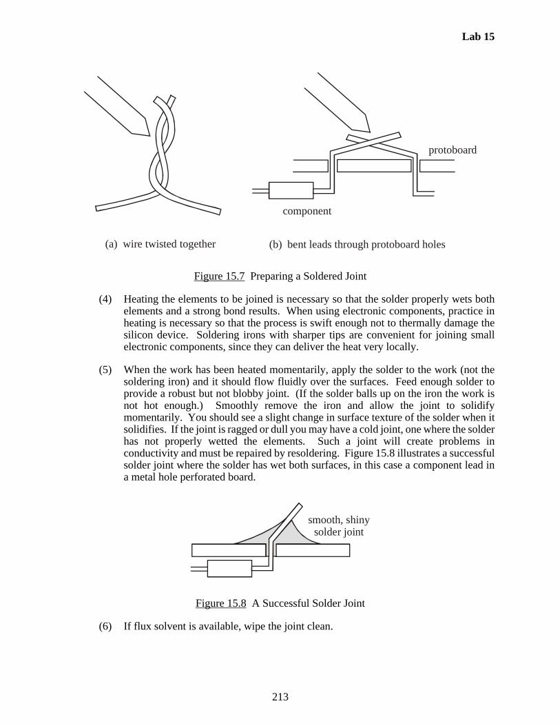
Lab 15
213
Figure 15.7 Preparing a Soldered Joint
(4) Heating the elements to be joined is necessary so that the solder properly wets bothelements and a strong bond results. When using electronic components, practice inheating is necessary so that the process is swift enough not to thermally damage thesilicon device. Soldering irons with sharper tips are convenient for joining smallelectronic components, since they can deliver the heat very locally.
(5) When the work has been heated momentarily, apply the solder to the work (not thesoldering iron) and it should flow fluidly over the surfaces. Feed enough solder toprovide a robust but not blobby joint. (If the solder balls up on the iron the work isnot hot enough.) Smoothly remove the iron and allow the joint to solidifymomentarily. You should see a slight change in surface texture of the solder when itsolidifies. If the joint is ragged or dull you may have a cold joint, one where the solderhas not properly wetted the elements. Such a joint will create problems inconductivity and must be repaired by resoldering. Figure 15.8 illustrates a successfulsolder joint where the solder has wet both surfaces, in this case a component lead ina metal hole perforated board.
Figure 15.8 A Successful Solder Joint
(6) If flux solvent is available, wipe the joint clean.
(a) wire twisted together (b) bent leads through protoboard holes
component
protoboard
smooth, shinysolder joint
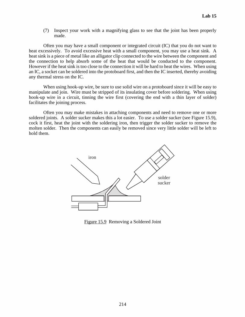
Lab 15
214
(7) Inspect your work with a magnifying glass to see that the joint has been properlymade.
Often you may have a small component or integrated circuit (IC) that you do not want toheat excessively. To avoid excessive heat with a small component, you may use a heat sink. Aheat sink is a piece of metal like an alligator clip connected to the wire between the component andthe connection to help absorb some of the heat that would be conducted to the component.However if the heat sink is too close to the connection it will be hard to heat the wires. When usingan IC, a socket can be soldered into the protoboard first, and then the IC inserted, thereby avoidingany thermal stress on the IC.
When using hook-up wire, be sure to use solid wire on a protoboard since it will be easy tomanipulate and join. Wire must be stripped of its insulating cover before soldering. When usinghook-up wire in a circuit, tinning the wire first (covering the end with a thin layer of solder)facilitates the joining process.
Often you may make mistakes in attaching components and need to remove one or moresoldered joints. A solder sucker makes this a lot easier. To use a solder sucker (see Figure 15.9),cock it first, heat the joint with the soldering iron, then trigger the solder sucker to remove themolten solder. Then the components can easily be removed since very little solder will be left tohold them.
Figure 15.9 Removing a Soldered Joint
iron
soldersucker

Lab 15
215
15.5 Other Practical Considerations
For basic prototype circuit assembly and troubleshooting advice, see Section 2.3 inLab 2 and Section 7.4 in Lab 7. For advice for debugging circuits with PIC microcontrollers,see Section 10.4 in Lab 10.
Here are some other practical suggestions for microcontroller-based designs:
General Electrical Design Suggestions:
• When ordering ICs, make sure you specify DIP (dual in-line packages) and not surfacemount packages (e.g., SOP). DIP chips are well suited to use in breadboards andprotoboards. Surface mount ICs require printed circuit boards (PCBs) and specialsoldering equipment.
• Make sure your power supply (or supplies) can provide adequate current for the entiredesign. If necessary, use separate power supplies for your signal and power circuits.
• Use breadboards with caution and care because connections can be unreliable, and thebase plate adds capacitance to your circuits. Hard-wired and soldered protoboards orprinted circuit boards (PCBs) can be much more reliable. See Section15.4 for advice onhow to solder properly. Be sure to use sockets for all ICs to prevent damage duringsoldering and to allow easy replacement of the ICs. Also, if you have a workingbreadboard circuit, it is advisable to use duplicate components (where possible) for thesoldered board (i.e., don’t cannibalize components from a working prototype circuit incase something goes wrong or gets damaged when soldering your board).
• Use a storage capacitor (e.g., 100 F or bigger) across the main power and groundlines of a power supply that does not have built-in output capacitance (e.g., batteries,wall transformers, and regulated voltages) to minimize voltage swings during outputcurrent spikes. Also, use bypass capacitors (e.g., 0.1 F) across the power andgrounds lines of all individual ICs to suppress any current and voltage spikes.
• Make sure all components and sources have a common ground unless using relays,wireless interfaces, or opto-isolators, in which case you should keep the independentpower supply grounds separate.
• Avoid grounding problems and electromagnetic interference (EMI). Section 2.10in the textbook presents various methods to reduce EMI, specifically using opto-isolators, single point grounding, ground planes, coaxial or twisted pair cables, andbypass capacitors.
• Don’t leave IC pins floating (especially with CMOS devices). In other words, connectall used and functional pins to signals or power or ground. As an example, do notassume that leaving a microcontroller’s reset pin disconnected will keep amicrocontroller from resetting itself. You should connect the reset pin to 5V for anactive-low reset or ground for an active-high reset, and not leave the pin floating whereits state can be uncertain.
• Be aware of possible switch bounce in your digital circuits and add debounce circuits

Lab 15
216
or software to eliminate the bounce.
• Use flyback diodes on motors, solenoids, relay coils, and other high inductance devicesthat are being switched.
• Use buffers, line drivers, and inverters where current demand is large for a digitaloutput.
• Use Schmitt triggers on all noisy digital sensor outputs (e.g., a Hall-effect proximitysensor or photo-interrupter).
• Use a common-emitter configuration with transistors (i.e., put the load on the highside) to avoid voltage biasing difficulties.
• Be careful to identify and properly interface any open-collector or open-drain outputson digital ICs (e.g., pin RA4 on the PIC).
• For reversible dc motors, use "off-the-shelf" commercially available H-bridge drivers(e.g., National Semiconductor’s LMD 18200) instead of building your own.
PIC-related Suggestions (see more in Section 10.4 of Lab 10):
• Follow the microcontroller design procedure in Section 7.9 of the textbook.
• Modularize your software and independently develop and test each module (i.e., don’twrite the entire program at once expecting it to work).
• Use LEDs to indicate status and location within your program when it is running, andto indicate input and output states.
• Be aware of the different characteristics of the I/O pins on the PIC. Refer to Figures7.15 and 7.16 in the textbook to see how to properly interface to the different pins fordifferent purposes.
• Be aware that PicBasic Pro commands totally occupy the processor while they arerunning (e.g., the line after a SOUND command is not reached or processed until theSOUND command has terminated).
• Refer to Design Example 7.1 in the textbook for ideas on how to interface to 7-segmentdigital displays with a minimum number of pins.
• When prototyping with a soldered protoboard or printed circuit board, use IC socketsto allow easy installation and removal of the PICs without damaging pins. Also, alwaysuse a "chip puller" tool to remove ICs (e.g., PICs) from breadboards or soldered ICsockets.
Related Documents