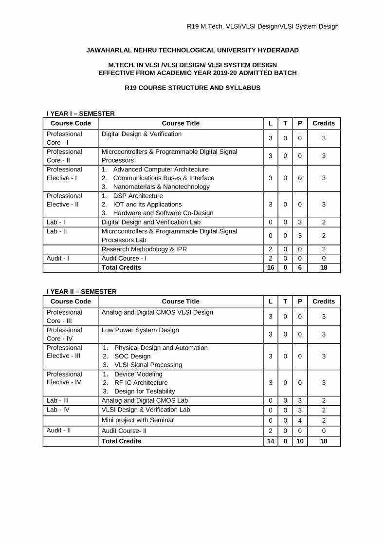
R19 M.Tech. VLSI/VLSI Design/VLSI System Design JAWAHARLAL NEHRU TECHNOLOGICAL UNIVERSITY HYDERABAD M.TECH. IN VLSI /VLSI DESIGN/ VLSI SYSTEM DESIGN EFFECTIVE FROM ACADEMIC YEAR 2019-20 ADMITTED BATCH R19 COURSE STRUCTURE AND SYLLABUS I YEAR I – SEMESTER Course Code Course Title L T P Credits Professional Core - I Digital Design & Verification 3 0 0 3 Professional Core - II Microcontrollers & Programmable Digital Signal Processors 3 0 0 3 Professional Elective - I 1. Advanced Computer Architecture 2. Communications Buses & Interface 3. Nanomaterials & Nanotechnology 3 0 0 3 Professional Elective - II 1. DSP Architecture 2. IOT and its Applications 3. Hardware and Software Co-Design 3 0 0 3 Lab - I Digital Design and Verification Lab 0 0 3 2 Lab - II Microcontrollers & Programmable Digital Signal Processors Lab 0 0 3 2 Research Methodology & IPR 2 0 0 2 Audit - I Audit Course - I 2 0 0 0 Total Credits 16 0 6 18 I YEAR II – SEMESTER Course Code Course Title L T P Credits Professional Core - III Analog and Digital CMOS VLSI Design 3 0 0 3 Professional Core - IV Low Power System Design 3 0 0 3 Professional Elective - III 1. Physical Design and Automation 2. SOC Design 3. VLSI Signal Processing 3 0 0 3 Professional Elective - IV 1. Device Modeling 2. RF IC Architecture 3. Design for Testability 3 0 0 3 Lab - III Analog and Digital CMOS Lab 0 0 3 2 Lab - IV VLSI Design & Verification Lab 0 0 3 2 Mini project with Seminar 0 0 4 2 Audit - II Audit Course- II 2 0 0 0 Total Credits 14 0 10 18

Welcome message from author
This document is posted to help you gain knowledge. Please leave a comment to let me know what you think about it! Share it to your friends and learn new things together.
Transcript
R19 M.Tech. VLSI/VLSI Design/VLSI System Design
JAWAHARLAL NEHRU TECHNOLOGICAL UNIVERSITY HYDERABAD
M.TECH. IN VLSI /VLSI DESIGN/ VLSI SYSTEM DESIGN EFFECTIVE FROM ACADEMIC YEAR 2019-20 ADMITTED BATCH
R19 COURSE STRUCTURE AND SYLLABUS
I YEAR I – SEMESTER
Course Code Course Title L T P Credits Professional Core - I
Digital Design & Verification 3 0 0 3
Professional Core - II
Microcontrollers & Programmable Digital Signal Processors 3 0 0 3
Professional Elective - I
1. Advanced Computer Architecture 2. Communications Buses & Interface 3. Nanomaterials & Nanotechnology
3 0 0 3
Professional Elective - II
1. DSP Architecture 2. IOT and its Applications 3. Hardware and Software Co-Design
3 0 0 3
Lab - I Digital Design and Verification Lab 0 0 3 2 Lab - II Microcontrollers & Programmable Digital Signal
Processors Lab 0 0 3 2
Research Methodology & IPR 2 0 0 2 Audit - I Audit Course - I 2 0 0 0 Total Credits 16 0 6 18 I YEAR II – SEMESTER
Course Code Course Title L T P Credits Professional Core - III
Analog and Digital CMOS VLSI Design 3 0 0 3
Professional Core - IV
Low Power System Design 3 0 0 3
Professional Elective - III
1. Physical Design and Automation 2. SOC Design 3. VLSI Signal Processing
3 0 0 3
Professional Elective - IV
1. Device Modeling 2. RF IC Architecture 3. Design for Testability
3 0 0 3
Lab - III Analog and Digital CMOS Lab 0 0 3 2 Lab - IV VLSI Design & Verification Lab 0 0 3 2
Mini project with Seminar 0 0 4 2 Audit - II Audit Course- II 2 0 0 0 Total Credits 14 0 10 18
R19 M.Tech. VLSI/VLSI Design/VLSI System Design
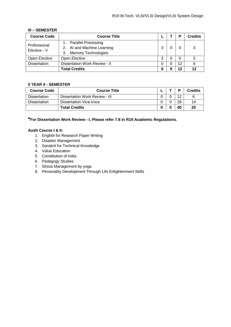
III – SEMESTER Course Code Course Title L T P Credits
Professional Elective - V
1. Parallel Processing 2. AI and Machine Learning 3. Memory Technologies
3 0 0 3
Open Elective Open Elective 3 0 0 3 Dissertation Dissertation Work Review - II 0 0 12 6
Total Credits 6 0 12 12 II YEAR II - SEMESTER Course Code Course Title L T P Credits
Dissertation Dissertation Work Review - III 0 0 12 6 Dissertation Dissertation Viva-Voce 0 0 28 14
Total Credits 0 0 40 20 *For Dissertation Work Review - I, Please refer 7.8 in R19 Academic Regulations. Audit Course I & II:
1. English for Research Paper Writing 2. Disaster Management 3. Sanskrit for Technical Knowledge 4. Value Education 5. Constitution of India 6. Pedagogy Studies 7. Stress Management by yoga 8. Personality Development Through Life Enlightenment Skills
R19 M.Tech. VLSI/VLSI Design/VLSI System Design
JAWAHARLAL NEHRU TECHNOLOGICAL UNIVERSITY HYDERABAD
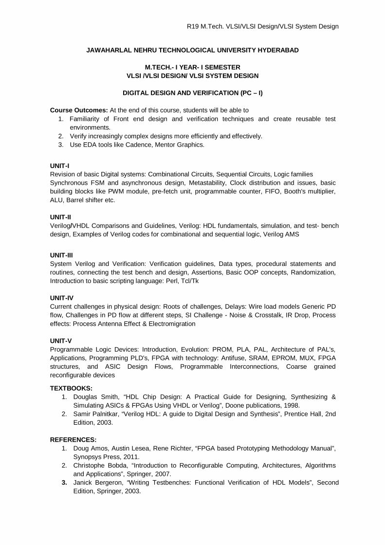
M.TECH.- I YEAR- I SEMESTER VLSI /VLSI DESIGN/ VLSI SYSTEM DESIGN
DIGITAL DESIGN AND VERIFICATION (PC – I)
Course Outcomes: At the end of this course, students will be able to
1. Familiarity of Front end design and verification techniques and create reusable test environments.
2. Verify increasingly complex designs more efficiently and effectively. 3. Use EDA tools like Cadence, Mentor Graphics.
UNIT-I Revision of basic Digital systems: Combinational Circuits, Sequential Circuits, Logic families Synchronous FSM and asynchronous design, Metastability, Clock distribution and issues, basic building blocks like PWM module, pre-fetch unit, programmable counter, FIFO, Booth's multiplier, ALU, Barrel shifter etc. UNIT-II Verilog/VHDL Comparisons and Guidelines, Verilog: HDL fundamentals, simulation, and test- bench design, Examples of Verilog codes for combinational and sequential logic, Verilog AMS
UNIT-III System Verilog and Verification: Verification guidelines, Data types, procedural statements and routines, connecting the test bench and design, Assertions, Basic OOP concepts, Randomization, Introduction to basic scripting language: Perl, Tcl/Tk UNIT-IV Current challenges in physical design: Roots of challenges, Delays: Wire load models Generic PD flow, Challenges in PD flow at different steps, SI Challenge - Noise & Crosstalk, IR Drop, Process effects: Process Antenna Effect & Electromigration UNIT-V Programmable Logic Devices: Introduction, Evolution: PROM, PLA, PAL, Architecture of PAL's, Applications, Programming PLD's, FPGA with technology: Antifuse, SRAM, EPROM, MUX, FPGA structures, and ASIC Design Flows, Programmable Interconnections, Coarse grained reconfigurable devices
TEXTBOOKS: 1. Douglas Smith, “HDL Chip Design: A Practical Guide for Designing, Synthesizing &
Simulating ASICs & FPGAs Using VHDL or Verilog”, Doone publications, 1998. 2. Samir Palnitkar, “Verilog HDL: A guide to Digital Design and Synthesis”, Prentice Hall, 2nd
Edition, 2003. REFERENCES:
1. Doug Amos, Austin Lesea, Rene Richter, “FPGA based Prototyping Methodology Manual”, Synopsys Press, 2011.
2. Christophe Bobda, “Introduction to Reconfigurable Computing, Architectures, Algorithms and Applications”, Springer, 2007.
3. Janick Bergeron, “Writing Testbenches: Functional Verification of HDL Models”, Second Edition, Springer, 2003.
R19 M.Tech. VLSI/VLSI Design/VLSI System Design
JAWAHARLAL NEHRU TECHNOLOGICAL UNIVERSITY HYDERABAD
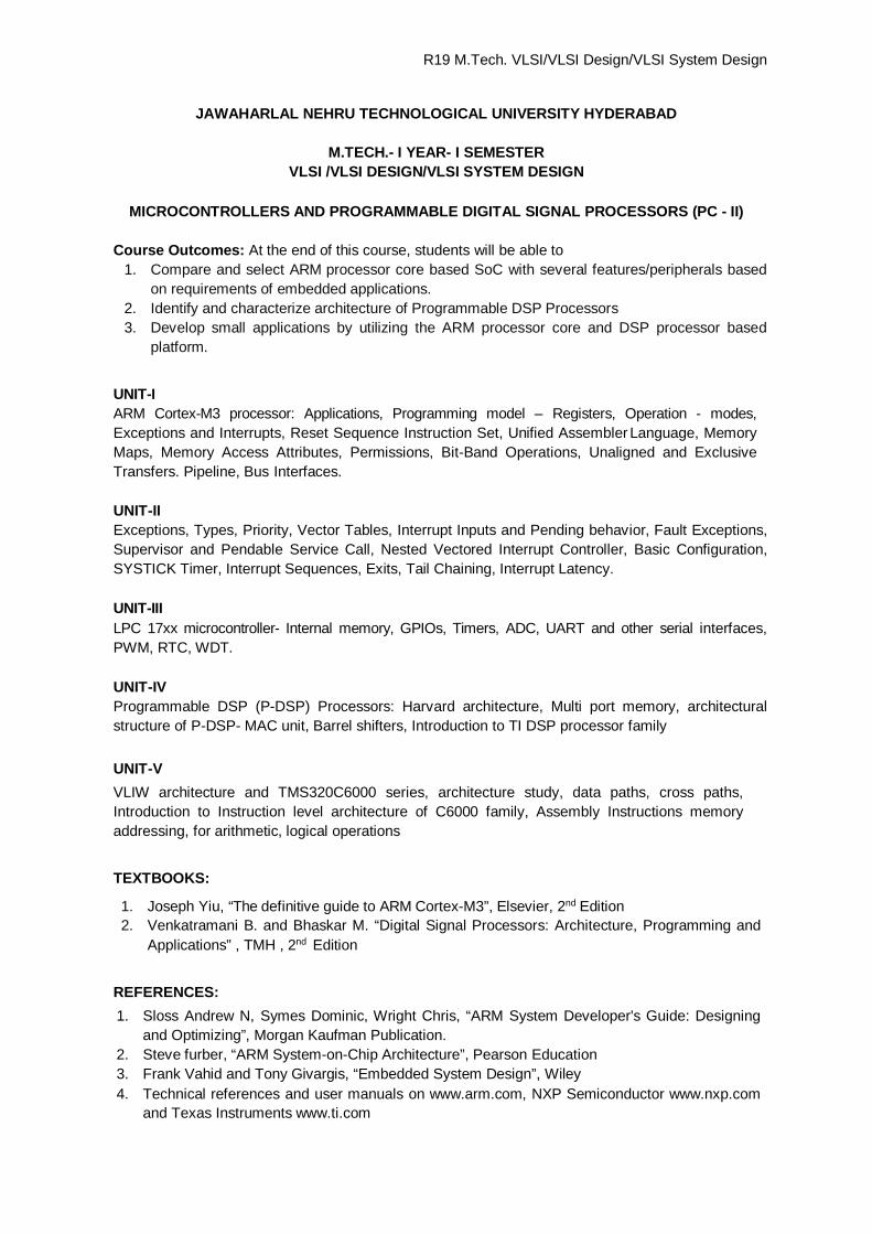
M.TECH.- I YEAR- I SEMESTER VLSI /VLSI DESIGN/VLSI SYSTEM DESIGN
MICROCONTROLLERS AND PROGRAMMABLE DIGITAL SIGNAL PROCESSORS (PC - II)
Course Outcomes: At the end of this course, students will be able to
1. Compare and select ARM processor core based SoC with several features/peripherals based on requirements of embedded applications.
2. Identify and characterize architecture of Programmable DSP Processors 3. Develop small applications by utilizing the ARM processor core and DSP processor based
platform.
UNIT-I ARM Cortex-M3 processor: Applications, Programming model – Registers, Operation - modes, Exceptions and Interrupts, Reset Sequence Instruction Set, Unified Assembler Language, Memory Maps, Memory Access Attributes, Permissions, Bit-Band Operations, Unaligned and Exclusive Transfers. Pipeline, Bus Interfaces. UNIT-II Exceptions, Types, Priority, Vector Tables, Interrupt Inputs and Pending behavior, Fault Exceptions, Supervisor and Pendable Service Call, Nested Vectored Interrupt Controller, Basic Configuration, SYSTICK Timer, Interrupt Sequences, Exits, Tail Chaining, Interrupt Latency. UNIT-III LPC 17xx microcontroller- Internal memory, GPIOs, Timers, ADC, UART and other serial interfaces, PWM, RTC, WDT. UNIT-IV Programmable DSP (P-DSP) Processors: Harvard architecture, Multi port memory, architectural structure of P-DSP- MAC unit, Barrel shifters, Introduction to TI DSP processor family UNIT-V VLIW architecture and TMS320C6000 series, architecture study, data paths, cross paths, Introduction to Instruction level architecture of C6000 family, Assembly Instructions memory addressing, for arithmetic, logical operations TEXTBOOKS:
1. Joseph Yiu, “The definitive guide to ARM Cortex-M3”, Elsevier, 2nd Edition 2. Venkatramani B. and Bhaskar M. “Digital Signal Processors: Architecture, Programming and
Applications” , TMH , 2nd Edition REFERENCES: 1. Sloss Andrew N, Symes Dominic, Wright Chris, “ARM System Developer's Guide: Designing
and Optimizing”, Morgan Kaufman Publication. 2. Steve furber, “ARM System-on-Chip Architecture”, Pearson Education 3. Frank Vahid and Tony Givargis, “Embedded System Design”, Wiley 4. Technical references and user manuals on www.arm.com, NXP Semiconductor www.nxp.com
and Texas Instruments www.ti.com
R19 M.Tech. VLSI/VLSI Design/VLSI System Design
JAWAHARLAL NEHRU TECHNOLOGICAL UNIVERSITY HYDERABAD
M.TECH.- I YEAR- I SEMESTER VLSI/VLSI DESIGN/VLSI SYSTEM DESIGN
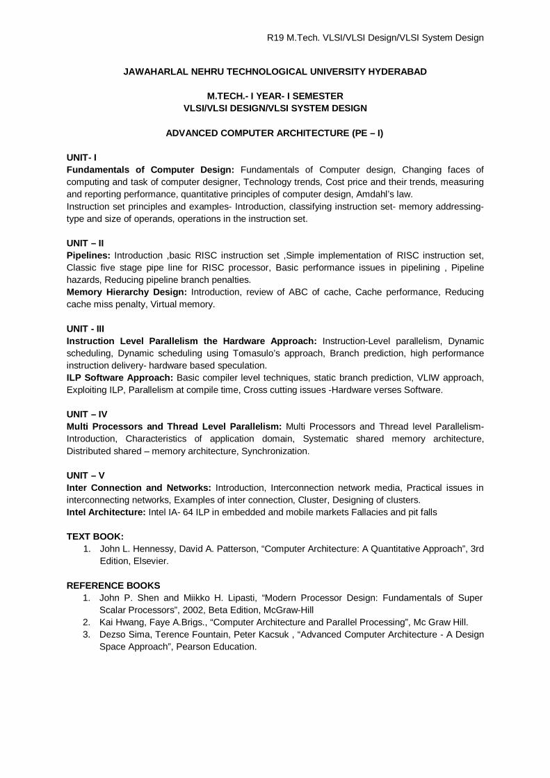
ADVANCED COMPUTER ARCHITECTURE (PE – I)
UNIT- I Fundamentals of Computer Design: Fundamentals of Computer design, Changing faces of computing and task of computer designer, Technology trends, Cost price and their trends, measuring and reporting performance, quantitative principles of computer design, Amdahl’s law. Instruction set principles and examples- Introduction, classifying instruction set- memory addressing- type and size of operands, operations in the instruction set. UNIT – II Pipelines: Introduction ,basic RISC instruction set ,Simple implementation of RISC instruction set, Classic five stage pipe line for RISC processor, Basic performance issues in pipelining , Pipeline hazards, Reducing pipeline branch penalties. Memory Hierarchy Design: Introduction, review of ABC of cache, Cache performance, Reducing cache miss penalty, Virtual memory. UNIT - III Instruction Level Parallelism the Hardware Approach: Instruction-Level parallelism, Dynamic scheduling, Dynamic scheduling using Tomasulo’s approach, Branch prediction, high performance instruction delivery- hardware based speculation. ILP Software Approach: Basic compiler level techniques, static branch prediction, VLIW approach, Exploiting ILP, Parallelism at compile time, Cross cutting issues -Hardware verses Software. UNIT – IV Multi Processors and Thread Level Parallelism: Multi Processors and Thread level Parallelism- Introduction, Characteristics of application domain, Systematic shared memory architecture, Distributed shared – memory architecture, Synchronization. UNIT – V Inter Connection and Networks: Introduction, Interconnection network media, Practical issues in interconnecting networks, Examples of inter connection, Cluster, Designing of clusters. Intel Architecture: Intel IA- 64 ILP in embedded and mobile markets Fallacies and pit falls TEXT BOOK:
1. John L. Hennessy, David A. Patterson, “Computer Architecture: A Quantitative Approach”, 3rd Edition, Elsevier.
REFERENCE BOOKS
1. John P. Shen and Miikko H. Lipasti, “Modern Processor Design: Fundamentals of Super Scalar Processors”, 2002, Beta Edition, McGraw-Hill
2. Kai Hwang, Faye A.Brigs., “Computer Architecture and Parallel Processing”, Mc Graw Hill. 3. Dezso Sima, Terence Fountain, Peter Kacsuk , “Advanced Computer Architecture - A Design
Space Approach”, Pearson Education.
R19 M.Tech. VLSI/VLSI Design/VLSI System Design
JAWAHARLAL NEHRU TECHNOLOGICAL UNIVERSITY HYDERABAD
M.TECH.- I YEAR- I SEMESTER VLSI/VLSI DESIGN/VLSI SYSTEM DESIGN
COMMUNICATION BUSES AND INTERFACES (PE – I)
Course Outcomes: At the end of the course, students will be able to:
1. Select a particular serial bus suitable for a particular application. 2. Develop APIs for configuration, reading and writing data onto serial bus. 3. Design and develop peripherals that can be interfaced to desired serial bus.
UNIT-I Serial Busses - Physical interface, Data and Control signals, features, limitations and applications of RS232, RS485, I2C, SPI UNIT-II CAN - Architecture, Data transmission, Layers, Frame formats, applications UNIT-III PCIe - Revisions, Configuration space, Hardware protocols, applications UNIT-IV USB - Transfer types, enumeration, Descriptor types and contents, Device driver UNIT-V Data Streaming Serial Communication Protocol - Serial Front Panel Data Port (SFPDP) using fiber optic and copper cable TEXTBOOKS:
1. Jan Axelson, “Serial Port Complete - COM Ports, USB Virtual Com Ports, and Ports for Embedded Systems”, Lakeview Research, 2nd Edition
2. Jan Axelson, “USB Complete”, Penram Publications 3. Mike Jackson, Ravi Budruk, “PCI Express Technology”, Mindshare Press 4. Wilfried Voss, “A Comprehensible Guide to Controller Area Network”, Copperhill Media
Corporation, 2nd Edition, 2005. 5. Serial Front Panel Draft Standard VITA 17.1 – 200x 6. Technical references on www.can-cia.org, www.pcisig.com, www.usb.org
R19 M.Tech. VLSI/VLSI Design/VLSI System Design
JAWAHARLAL NEHRU TECHNOLOGICAL UNIVERSITY HYDERABAD
M.TECH.- I YEAR- I SEMESTER VLSI/VLSI DESIGN/VLSI SYSTEM DESIGN
NANOMATERIALS AND NANOTECHNOLOGY (PE – I)
Course Outcomes: At the end of the course, students will be able to:
1. To understand the basic science behind the design and fabrication of nano scale systems. 2. To understand and formulate new engineering solutions for current problems and
competing technologies for future applications. 3. To be able make inter disciplinary projects applicable to wide areas by clearing and fixing the
boundaries in system development. 4. To gather detailed knowledge of the operation of fabrication and characterization devices to
achieve precisely designed systems UNIT I Introduction of nano materials and nanotechnologies, Features of nanostructures, Applications of nano materials and technologies. Nano dimensional Materials 0D, 1D, 2D structures – Size Effects – Fraction of Surface Atoms – Specific Surface Energy and Surface Stress – Effect on the Lattice Parameter – Phonon Density of States – the General Methods available for the Synthesis of Nanostructures – precipitative – reactive – hydrothermal/solvo thermal methods – suitability of such methods for scaling – potential Uses. UNIT II Fundamentals of nanomaterials, Classification, Zero-dimensional nanomaterials, One-dimensional nanomaterials, Two-dimensional nanomaterials, Three dimensional nanomaterials. Low-Dimensional Nanomaterials and its Applications, Synthesis, Properties, and Applications of Low-Dimensional Carbon-Related Nanomaterials. UNIT III Micro- and Nanolithography Techniques, Emerging Applications Introduction to Micro electro mechanical Systems (MEMS), Advantages and Challenges of MEMS, Fabrication Technologies, Surface Micromachining, Bulk Micromachining, Molding. Introduction to Nano Phonics. UNIT IV Introduction, Synthesis of CNTs - Arc-discharge, Laser-ablation, Catalytic growth, Growth mechanisms of CNT’s - Multi-walled nanotubes, Single-walled nanotubes Optical properties of CNT’s, Electrical transport in perfect nanotubes, Applications as case studies. Synthesis and Applications of CNT's. UNIT V Ferroelectric materials, coating, molecular electronics and nanoelectronics, biological and environmental, membrane based application, polymer based application. TEXT BOOKS
1. Kenneth J. Klabunde and Ryan M. Richards, “Nanoscale Materials in Chemistry”, 2 edition, John Wiley and Sons, 2009.
2. I Gusev and A A Rempel, “Nanocrystalline Materials”, Cambridge International Science Publishing, 1 st Indian edition by Viva Books Pvt. Ltd. 2008.
R19 M.Tech. VLSI/VLSI Design/VLSI System Design
3. B. S. Murty, P. Shankar, Baldev Raj, B. B. Rath, James Murday, “Nanoscience and Nanotechnology”, Tata McGraw Hill Education 2012.
REFERENCE BOOKS
1. Bharat Bhushan, “Springer Handbook of Nanotechnology”, Springer, 3rd edition, 2010. 2. Kamal K. Kar, “Carbon Nanotubes: Synthesis, Characterization and Applications”,
Research Publishing Services; 1 st edition, 2011, ISBN-13: 978-9810863975.
R19 M.Tech. VLSI/VLSI Design/VLSI System Design
JAWAHARLAL NEHRU TECHNOLOGICAL UNIVERSITY HYDERABAD
M.TECH.- I YEAR- I SEMESTER VLSI/VLSI DESIGN/VLSI SYSTEM DESIGN
DSP ARCHITECTURE (PE – II)
Course Outcomes:
1. At the end of this course, students will be able to Identify and formalize architectural level characterization of P-DSP hardware
2. Ability to design, programming (assembly and C), and testing code using Code Composer Studio environment
3. Deployment of DSP hardware for Control, Audio and Video Signal processing applications Understanding of major areas and challenges in DSP based embedded systems
UNIT-I Programmable DSP Hardware: Processing Architectures (von Neumann, Harvard), DSP core algorithms (FIR, IIR, Convolution, Correlation, FFT), IEEE standard for Fixed and Floating Point Computations, Special Architectures Modules used in Digital Signal Processors (like MAC unit, Barrel shifters), On-Chip peripherals, DSP benchmarking. UNIT-II Structural and Architectural Considerations: Parallelism in DSP processing, Texas Instruments TMS320 Digital Signal Processor Families, Fixed Point TI DSP Processors: TMS320C1X and TMS320C2X Family,TMS320C25 –Internal Architecture, Arithmetic and Logic Unit, Auxiliary Registers, Addressing Modes (Immediate, Direct and Indirect, Bit-reverse Addressing), Basics of TMS320C54x and C55x Families in respect of Architecture improvements and new applications fields, TMS320C5416 DSP Architecture, Memory Map, Interrupt System, Peripheral Devices, Illustrative Examples for assembly coding. UNIT-III VLIW Architecture: Current DSP Architectures, GPUs as an alternative to DSP Processors, TMS320C6X Family, Addressing Modes, Replacement of MAC unit by ILP, Detailed study of ISA, Assembly Language Programming, Code Composer Studio, Mixed Cand Assembly Language programming, On-chip peripherals, Simple applications developments as an embedded environment. UNIT-IV Multi-core DSPs: Introduction to Multi-core computing and applicability for DSP hardware, Concept of threads, introduction to P-thread, mutex and similar concepts, heterogeneous and homogenous multi-core systems. UNIT-V. Shared Memory parallel programming –OpenMP approach of parallel programming, PRAGMA directives, OpenMP Constructs for work sharing like for loop, sections, TI TMS320C6678 (Eight Core subsystem). REFERENCES:
1. M. Sasikumar, D. Shikhare, Ravi Prakash, “Introduction to Parallel Processing”, 1st Edition, PHI, 2006.
2. Fayez Gebali, “Algorithms and Parallel Computing”,1st Edition, John Wiley & Sons, 2011 3. Rohit Chandra, Ramesh Menon, Leo Dagum, David Kohr, Dror Maydan, Jeff McDonald,
“Parallel Programming in OpenMP”, 1st Edition, Morgan Kaufman,2000.
R19 M.Tech. VLSI/VLSI Design/VLSI System Design
4. Ann Melnichuk, Long Talk, “Multicore Embedded systems”, 1st Edition, CRC Press,2010. 5. Wayne Wolf, “High Performance Embedded Computing: Architectures, Applications and
Methodologies”, 1st Edition, Morgan Kaufman, 2006. 6. E.S. Gopi, “Algorithmic Collections for Digital Signal Processing Applications Using
MATLAB”, 1st Edition, Springer Netherlands,2007.
R19 M.Tech. VLSI/VLSI Design/VLSI System Design
JAWAHARLAL NEHRU TECHNOLOGICAL UNIVERSITY HYDERABAD
M.TECH.- I YEAR- I SEMESTER VLSI/VLSI DESIGN/VLSI SYSTEM DESIGN
IOT AND ITS APPLICATIONS (PE – II)
Course Outcomes: At the end of this course, students will be able to
1. Understand the concept of IOT and M2M 2. Study IOT architecture and applications in various fields 3. Study the security and privacy issues in IOT.
UNIT-I IoT& Web Technology The Internet of Things Today, Time for Convergence, Towards the IoT Universe, Internet of Things Vision, IoT Strategic Research and Innovation Directions, IoT Applications, Future Internet Technologies, Infrastructure, Networks and Communication, Processes, Data Management, Security, Privacy & Trust, Device Level Energy Issues, IoT Related Standardization, Recommendations on Research Topics. UNIT-II M2M to IoT – A Basic Perspective– Introduction, Some Definitions, M2M Value Chains, IoT Value Chains, An emerging industrial structure for IoT, The international driven global value chain and global information monopolies. M2M to IoT-An Architectural Overview– Building an architecture, Main design principles and needed capabilities, An IoT architecture outline, standards considerations. UNIT-III IoT Architecture -State of the Art – Introduction, State of the art, Architecture Reference Model- Introduction, Reference Model and architecture, IoT reference Model, IoT Reference Architecture- Introduction, Functional View, Information View, Deployment and Operational View, Other Relevant architectural views. UNIT-IV IoT Applications for Value Creations Introduction, IoT applications for industry: Future Factory Concepts, Brownfield IoT, Smart Objects, Smart Applications, Four Aspects in your Business to Master IoT, Value Creation from Big Data and Serialization, IoT for Retailing Industry, IoT For Oil and Gas Industry, Opinions on IoT Application and Value for Industry, Home Management, eHealth. UNIT-V Internet of Things Privacy, Security and Governance Introduction, Overview of Governance, Privacy and Security Issues, TEXTBOOKS
1. Vijay Madisetti and Arshdeep Bahga, “Internet of Things (A Hands-on-Approach)”, 1st Edition, VPT, 2014.
2. Francis daCosta, “Rethinking the Internet of Things: A Scalable Approach to Connecting Everything”, 1st Edition, Apress Publications, 2013.
3. Cuno Pfister, “Getting Started with the Internet of Things”, O Reilly Media, 2011.
R19 M.Tech. VLSI/VLSI Design/VLSI System Design
JAWAHARLAL NEHRU TECHNOLOGICAL UNIVERSITY HYDERABAD
M.TECH.- I YEAR- I SEMESTER VLSI/VLSI DESIGN/VLSI SYSTEM DESIGN
HARDWARE AND SOFTWARE CO-DESIGN (PE – II)
Course Outcomes:
1. To acquire the knowledge on various models of Co-design. 2. To explore the interrelationship between Hardware and software in a embedded system 3. To acquire the knowledge of firmware development process and tools during Co-design. 4. Understand validation methods and adaptability.
UNIT I Co- Design Issues: Co- Design Models, Architectures, Languages, A Generic Co-design Methodology. Co- Synthesis Algorithms: Hardware software synthesis algorithms: hardware – software partitioning distributed system co-synthesis. UNIT II Prototyping and Emulation: Prototyping and emulation techniques, prototyping and emulation environments, future developments in emulation and prototyping architecture specialization techniques, system communication infrastructure. Target Architectures: Architecture Specialization techniques, System Communication infrastructure, Target Architecture and Application System classes, Architecture for control dominated systems (8051-Architectures for High performance control), Architecture for Data dominated systems (ADSP21060, TMS320C60), Mixed Systems. UNIT III Compilation Techniques and Tools for Embedded Processor Architectures: Modern embedded architectures, embedded software development needs, compilation technologies, practical consideration in a compiler development environment. UNIT IV Design Specification and Verification: Design, co-design, the co-design computational model, concurrency coordinating concurrent computations, interfacing components, design verification, implementation verification, verification tools, interface verification. UNIT V Languages for System – Level Specification and Design-I: System – level specification, design representation for system level synthesis, system level specification languages, Languages for System – Level Specification and Design-II: Heterogeneous specifications and multi-language co-simulation, the cosyma system and lycos system. REFERENCES:
1. Hardware / Software Co- Design Principles and Practice – Jorgen Staunstrup, Wayne Wolf –Springer, 2009.
2. Hardware / Software Co- Design - Giovanni De Micheli, Mariagiovanna Sami,Kluwer Academic Publishers, 2002.
3. A Practical Introduction to Hardware/Software Co-design -Patrick R. Schaumont, Springer, 2010
R19 M.Tech. VLSI/VLSI Design/VLSI System Design
JAWAHARLAL NEHRU TECHNOLOGICAL UNIVERSITY HYDERABAD
M.TECH.- I YEAR- I SEMESTER VLSI/VLSI DESIGN/VLSI SYSTEM DESIGN
DIGITAL DESIGN AND VERIFICATION LAB (Lab – I)
Course Objectives:
• To provide familiarity with hardware description language Verilog HDL for modelling of combinational and sequential circuits.
• To understand the role of functional simulator in the validating the functionality of designed circuits.
• To understand the Synthesis of a designed digital circuits. • To introduce the process of implementation of digital circuits on FPGA kits.
Course Outcomes: After completing this course the student will be able to
• Apply CAD tools for the design of digital circuits. • Appreciate the process of synthesizing a given digital circuits. • Implement the specified digital circuits using FPGA.
Implementation of the following designs on FPGA using Verilog HDL:
1. 8:1 Mux/Demux, Full Adder, 8-bit Magnitude comparator, Encoder/decoder, Priority encoder, Parity generator
2. Code converters 3. D-FF, 4-bit Shift registers (SISO, SIPO, PISO, bidirectional), 3-bit Synchronous Counters. 4. Sequence generator/detectors, Synchronous FSM – Mealy and Moore machines. 5. Vending machines - Traffic Light controller, ATM, elevator control. 6. PCI Bus &Arbiter. 7. Single and Dual port SRAM 8. Arithmetic circuits like serial adder/ subtractor, parallel adder/subtractor, serial/parallel
multiplier.
R19 M.Tech. VLSI/VLSI Design/VLSI System Design
JAWAHARLAL NEHRU TECHNOLOGICAL UNIVERSITY HYDERABAD
M.TECH.- I YEAR- I SEMESTER VLSI/VLSI DESIGN/VLSI SYSTEM DESIGN
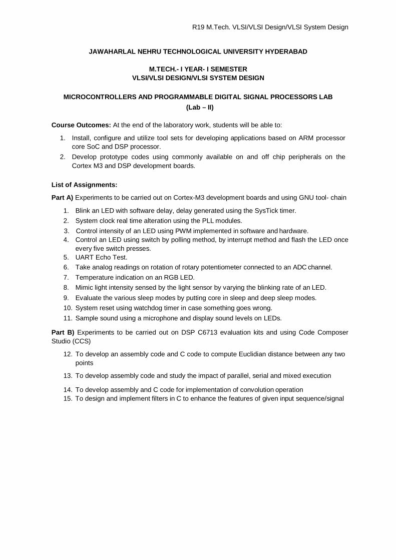
MICROCONTROLLERS AND PROGRAMMABLE DIGITAL SIGNAL PROCESSORS LAB
(Lab – II) Course Outcomes: At the end of the laboratory work, students will be able to:
1. Install, configure and utilize tool sets for developing applications based on ARM processor core SoC and DSP processor.
2. Develop prototype codes using commonly available on and off chip peripherals on the Cortex M3 and DSP development boards.
List of Assignments:
Part A) Experiments to be carried out on Cortex-M3 development boards and using GNU tool- chain
1. Blink an LED with software delay, delay generated using the SysTick timer. 2. System clock real time alteration using the PLL modules. 3. Control intensity of an LED using PWM implemented in software and hardware. 4. Control an LED using switch by polling method, by interrupt method and flash the LED once
every five switch presses. 5. UART Echo Test. 6. Take analog readings on rotation of rotary potentiometer connected to an ADC channel. 7. Temperature indication on an RGB LED. 8. Mimic light intensity sensed by the light sensor by varying the blinking rate of an LED. 9. Evaluate the various sleep modes by putting core in sleep and deep sleep modes. 10. System reset using watchdog timer in case something goes wrong. 11. Sample sound using a microphone and display sound levels on LEDs.
Part B) Experiments to be carried out on DSP C6713 evaluation kits and using Code Composer Studio (CCS)
12. To develop an assembly code and C code to compute Euclidian distance between any two points
13. To develop assembly code and study the impact of parallel, serial and mixed execution
14. To develop assembly and C code for implementation of convolution operation 15. To design and implement filters in C to enhance the features of given input sequence/signal
R19 M.Tech. VLSI/VLSI Design/VLSI System Design
JAWAHARLAL NEHRU TECHNOLOGICAL UNIVERSITY HYDERABAD
M.TECH.- I YEAR- I SEMESTER VLSI/VLSI DESIGN/VLSI SYSTEM DESIGN
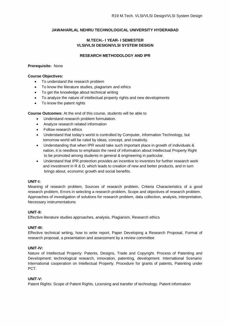
RESEARCH METHODOLOGY AND IPR
Prerequisite: None Course Objectives:
To understand the research problem To know the literature studies, plagiarism and ethics To get the knowledge about technical writing To analyze the nature of intellectual property rights and new developments To know the patent rights
Course Outcomes: At the end of this course, students will be able to
Understand research problem formulation. Analyze research related information Follow research ethics Understand that today’s world is controlled by Computer, Information Technology, but tomorrow world will be ruled by ideas, concept, and creativity. Understanding that when IPR would take such important place in growth of individuals & nation, it is needless to emphasis the need of information about Intellectual Property Right
to be promoted among students in general & engineering in particular. Understand that IPR protection provides an incentive to inventors for further research work and investment in R & D, which leads to creation of new and better products, and in turn
brings about, economic growth and social benefits.
UNIT-I: Meaning of research problem, Sources of research problem, Criteria Characteristics of a good research problem, Errors in selecting a research problem, Scope and objectives of research problem. Approaches of investigation of solutions for research problem, data collection, analysis, interpretation, Necessary instrumentations UNIT-II: Effective literature studies approaches, analysis, Plagiarism, Research ethics UNIT-III: Effective technical writing, how to write report, Paper Developing a Research Proposal, Format of research proposal, a presentation and assessment by a review committee
UNIT-IV: Nature of Intellectual Property: Patents, Designs, Trade and Copyright. Process of Patenting and Development: technological research, innovation, patenting, development. International Scenario: International cooperation on Intellectual Property. Procedure for grants of patents, Patenting under PCT.
UNIT-V: Patent Rights: Scope of Patent Rights. Licensing and transfer of technology. Patent information
R19 M.Tech. VLSI/VLSI Design/VLSI System Design
and databases. Geographical Indications. New Developments in IPR: Administration of Patent System. New developments in IPR; IPR of Biological Systems, Computer Software etc. Traditional knowledge Case Studies, IPR and IITs. TEXT BOOKS:
1. Stuart Melville and Wayne Goddard, “Research methodology: an introduction for science & engineering students’”
2. Wayne Goddard and Stuart Melville, “Research Methodology: An Introduction”
REFERENCES: 1. Ranjit Kumar, 2nd Edition, “Research Methodology: A Step by Step Guide for beginners” 2. Halbert, “Resisting Intellectual Property”, Taylor & Francis Ltd ,2007. 3. Mayall, “Industrial Design”, McGraw Hill, 1992. 4. Niebel, “Product Design”, McGraw Hill, 1974. 5. Asimov, “Introduction to Design”, Prentice Hall, 1962. 6. Robert P. Merges, Peter S. Menell, Mark A. Lemley, “Intellectual Property in New
Technological Age”, 2016. 7. T. Ramappa, “Intellectual Property Rights Under WTO”, S. Chand, 2008
R19 M.Tech. VLSI/VLSI Design/VLSI System Design
JAWAHARLAL NEHRU TECHNOLOGICAL UNIVERSITY HYDERABAD
M.TECH.- I YEAR- II SEMESTER VLSI/VLSI DESIGN/VLSI SYSTEM DESIGN
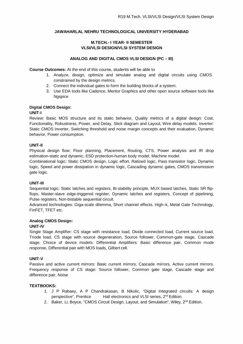
ANALOG AND DIGITAL CMOS VLSI DESIGN (PC – III)
Course Outcomes: At the end of this course, students will be able to
1. Analyze, design, optimize and simulate analog and digital circuits using CMOS constrained by the design metrics.
2. Connect the individual gates to form the building blocks of a system. 3. Use EDA tools like Cadence, Mentor Graphics and other open source software tools like
Ngspice Digital CMOS Design: UNIT-I Review: Basic MOS structure and its static behavior, Quality metrics of a digital design: Cost, Functionality, Robustness, Power, and Delay, Stick diagram and Layout, Wire delay models. Inverter: Static CMOS inverter, Switching threshold and noise margin concepts and their evaluation, Dynamic behavior, Power consumption. UNIT-II Physical design flow: Floor planning, Placement, Routing, CTS, Power analysis and IR drop estimation-static and dynamic, ESD protection-human body model, Machine model. Combinational logic: Static CMOS design, Logic effort, Ratioed logic, Pass transistor logic, Dynamic logic, Speed and power dissipation in dynamic logic, Cascading dynamic gates, CMOS transmission gate logic. UNIT-III Sequential logic: Static latches and registers, Bi-stability principle, MUX based latches, Static SR flip-flops, Master-slave edge-triggered register, Dynamic latches and registers, Concept of pipelining, Pulse registers, Non-bistable sequential circuit. Advanced technologies: Giga-scale dilemma, Short channel effects, High–k, Metal Gate Technology, FinFET, TFET etc. Analog CMOS Design: UNIT-IV Single Stage Amplifier: CS stage with resistance load, Divide connected load, Current source load, Triode load, CS stage with source degeneration, Source follower, Common-gate stage, Cascade stage, Choice of device models. Differential Amplifiers: Basic difference pair, Common mode response, Differential pair with MOS loads, Gilbert cell. UNIT-V Passive and active current mirrors: Basic current mirrors, Cascade mirrors, Active current mirrors. Frequency response of CS stage: Source follower, Common gate stage, Cascade stage and difference pair, Noise TEXTBOOKS:
1. J P Rabaey, A P Chandrakasan, B Nikolic, “Digital Integrated circuits: A design perspective”, Prentice Hall electronics and VLSI series, 2nd Edition.
2. Baker, Li, Boyce, “CMOS Circuit Design, Layout, and Simulation”, Wiley, 2nd Edition.
R19 M.Tech. VLSI/VLSI Design/VLSI System Design
REFERENCES: 1. BehzadRazavi , “Design of Analog CMOS Integrated Circuits”, TMH, 2007. 2. Phillip E. Allen and Douglas R. Holberg, “CMOS Analog Circuit Design”, Oxford, 3rd
Edition. 3. R J Baker, “CMOS circuit Design, Layout and Simulation”, IEEE Inc., 2008. 4. Kang, S. and Leblebici, Y., “CMOS Digital Integrated Circuits, Analysis and Design”,
TMH, 3rdEdition. 5. Pucknell, D.A. and Eshraghian, K., “Basic VLSI Design”, PHI, 3rd Edition
R19 M.Tech. VLSI/VLSI Design/VLSI System Design
JAWAHARLAL NEHRU TECHNOLOGICAL UNIVERSITY HYDERABAD
M.TECH.- I YEAR- II SEMESTER VLSI/VLSI DESIGN/VLSI SYSTEM DESIGN
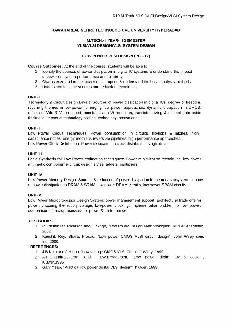
LOW POWER VLSI DESIGN (PC – IV)
Course Outcomes: At the end of the course, students will be able to:
1. Identify the sources of power dissipation in digital IC systems & understand the impact of power on system performance and reliability.
2. Characterize and model power consumption & understand the basic analysis methods. 3. Understand leakage sources and reduction techniques.
UNIT-I Technology & Circuit Design Levels: Sources of power dissipation in digital ICs, degree of freedom, recurring themes in low-power, emerging low power approaches, dynamic dissipation in CMOS, effects of Vdd & Vt on speed, constraints on Vt reduction, transistor sizing & optimal gate oxide thickness, impact of technology scaling, technology innovations. UNIT-II Low Power Circuit Techniques: Power consumption in circuits, flip-flops & latches, high capacitance nodes, energy recovery, reversible pipelines, high performance approaches. Low Power Clock Distribution: Power dissipation in clock distribution, single driver UNIT-III Logic Synthesis for Low Power estimation techniques: Power minimization techniques, low power arithmetic components- circuit design styles, adders, multipliers. UNIT-IV Low Power Memory Design: Sources & reduction of power dissipation in memory subsystem, sources of power dissipation in DRAM & SRAM, low power DRAM circuits, low power SRAM circuits. UNIT-V Low Power Microprocessor Design System: power management support, architectural trade offs for power, choosing the supply voltage, low-power clocking, implementation problem for low power, comparison of microprocessors for power & performance. TEXTBOOKS
1. P. Rashinkar, Paterson and L. Singh, “Low Power Design Methodologies”, Kluwer Academic, 2002
2. Kaushik Roy, Sharat Prasad, “Low power CMOS VLSI circuit design”, John Wiley sons Inc.,2000.
REFERENCES: 1. J.B.Kulo and J.H Lou, “Low voltage CMOS VLSI Circuits”, Wiley, 1999. 2. A.P.Chandrasekaran and R.W.Broadersen, “Low power digital CMOS design”,
Kluwer,1995 3. Gary Yeap, “Practical low power digital VLSI design”, Kluwer, 1998.
R19 M.Tech. VLSI/VLSI Design/VLSI System Design
JAWAHARLAL NEHRU TECHNOLOGICAL UNIVERSITY HYDERABAD
M.TECH.- I YEAR- II SEMESTER VLSI/VLSI DESIGN/VLSI SYSTEM DESIGN
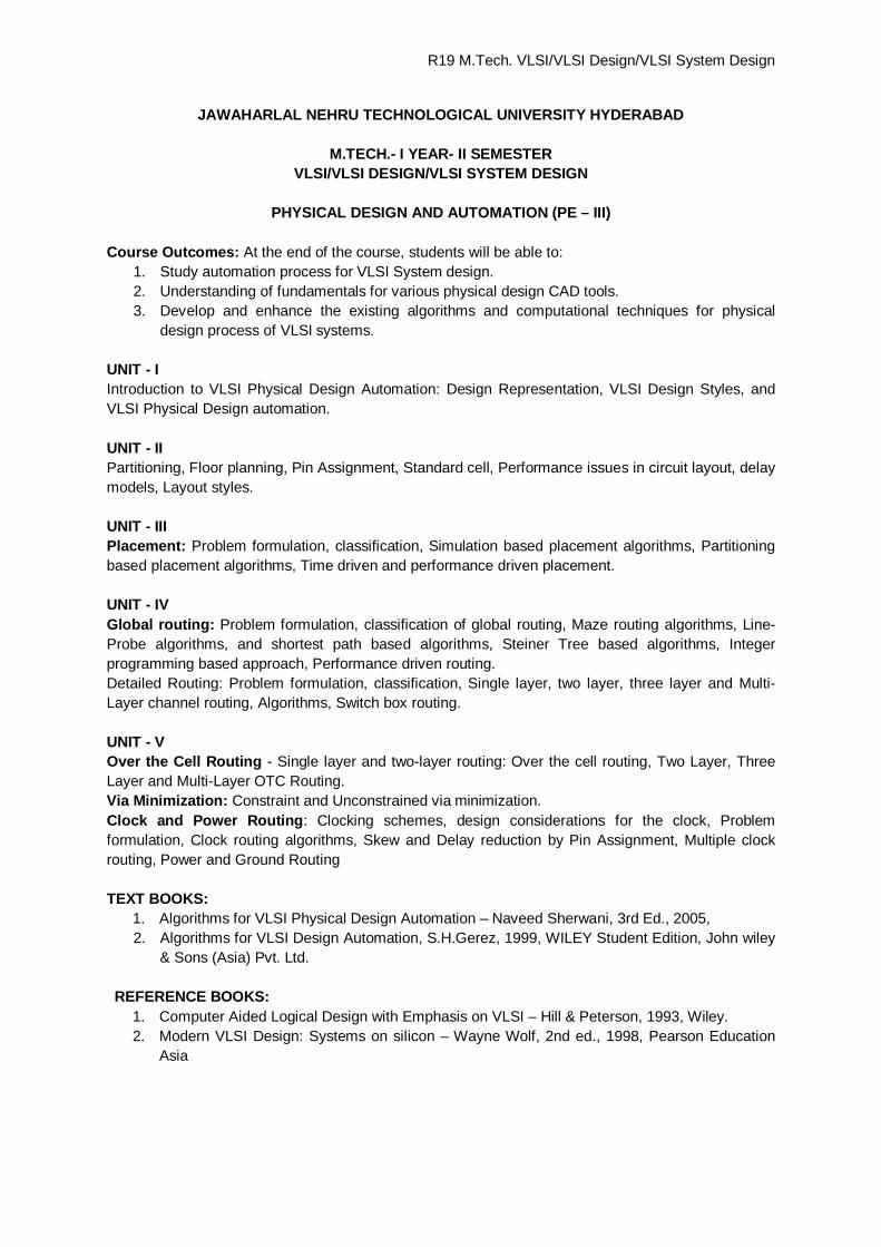
PHYSICAL DESIGN AND AUTOMATION (PE – III)
Course Outcomes: At the end of the course, students will be able to:
1. Study automation process for VLSI System design. 2. Understanding of fundamentals for various physical design CAD tools. 3. Develop and enhance the existing algorithms and computational techniques for physical
design process of VLSI systems. UNIT - I Introduction to VLSI Physical Design Automation: Design Representation, VLSI Design Styles, and VLSI Physical Design automation. UNIT - II Partitioning, Floor planning, Pin Assignment, Standard cell, Performance issues in circuit layout, delay models, Layout styles. UNIT - III Placement: Problem formulation, classification, Simulation based placement algorithms, Partitioning based placement algorithms, Time driven and performance driven placement. UNIT - IV Global routing: Problem formulation, classification of global routing, Maze routing algorithms, Line-Probe algorithms, and shortest path based algorithms, Steiner Tree based algorithms, Integer programming based approach, Performance driven routing. Detailed Routing: Problem formulation, classification, Single layer, two layer, three layer and Multi-Layer channel routing, Algorithms, Switch box routing. UNIT - V Over the Cell Routing - Single layer and two-layer routing: Over the cell routing, Two Layer, Three Layer and Multi-Layer OTC Routing. Via Minimization: Constraint and Unconstrained via minimization. Clock and Power Routing: Clocking schemes, design considerations for the clock, Problem formulation, Clock routing algorithms, Skew and Delay reduction by Pin Assignment, Multiple clock routing, Power and Ground Routing TEXT BOOKS:
1. Algorithms for VLSI Physical Design Automation – Naveed Sherwani, 3rd Ed., 2005, 2. Algorithms for VLSI Design Automation, S.H.Gerez, 1999, WILEY Student Edition, John wiley
& Sons (Asia) Pvt. Ltd. REFERENCE BOOKS:
1. Computer Aided Logical Design with Emphasis on VLSI – Hill & Peterson, 1993, Wiley. 2. Modern VLSI Design: Systems on silicon – Wayne Wolf, 2nd ed., 1998, Pearson Education
Asia
R19 M.Tech. VLSI/VLSI Design/VLSI System Design
JAWAHARLAL NEHRU TECHNOLOGICAL UNIVERSITY HYDERABAD
M.TECH.- I YEAR- II SEMESTER VLSI/VLSI DESIGN/VLSI SYSTEM DESIGN
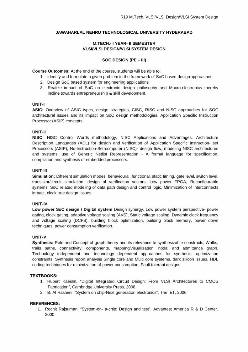
SOC DESIGN (PE – III)
Course Outcomes: At the end of the course, students will be able to:
1. Identify and formulate a given problem in the framework of SoC based design approaches 2. Design SoC based system for engineering applications 3. Realize impact of SoC on electronic design philosophy and Macro-electronics thereby
incline towards entrepreneurship & skill development.
UNIT-I ASIC: Overview of ASIC types, design strategies, CISC, RISC and NISC approaches for SOC architectural issues and its impact on SoC design methodologies, Application Specific Instruction Processor (ASIP) concepts. UNIT-II NISC: NISC Control Words methodology, NISC Applications and Advantages, Architecture Description Languages (ADL) for design and verification of Application Specific Instruction- set Processors (ASIP), No-Instruction-Set-computer (NISC)- design flow, modeling NISC architectures and systems, use of Generic Netlist Representation - A formal language for specification, compilation and synthesis of embedded processors. UNIT-III Simulation: Different simulation modes, behavioural, functional, static timing, gate level, switch level, transistor/circuit simulation, design of verification vectors, Low power FPGA, Reconfigurable systems, SoC related modeling of data path design and control logic, Minimization of interconnects impact, clock tree design issues. UNIT-IV Low power SoC design / Digital system Design synergy, Low power system perspective- power gating, clock gating, adaptive voltage scaling (AVS), Static voltage scaling, Dynamic clock frequency and voltage scaling (DCFS), building block optimization, building block memory, power down techniques, power consumption verification. UNIT-V Synthesis: Role and Concept of graph theory and its relevance to synthesizable constructs, Walks, trails paths, connectivity, components, mapping/visualization, nodal and admittance graph. Technology independent and technology dependent approaches for synthesis, optimization constraints, Synthesis report analysis Single core and Multi core systems, dark silicon issues, HDL coding techniques for minimization of power consumption, Fault tolerant designs
TEXTBOOKS: 1. Hubert Kaeslin, “Digital Integrated Circuit Design: From VLSI Architectures to CMOS
Fabrication”, Cambridge University Press, 2008. 2. B. Al Hashimi, “System on chip-Next generation electronics”, The IET, 2006
REFERENCES:
1. Rochit Rajsuman, “System-on- a-chip: Design and test”, Advantest America R & D Center, 2000
R19 M.Tech. VLSI/VLSI Design/VLSI System Design
2. P Mishra and N Dutt, “Processor Description Languages”, Morgan Kaufmann, 2008 3. Michael J. Flynn and Wayne Luk, “Computer System Design: System-on-Chip”. Wiley, 2011
R19 M.Tech. VLSI/VLSI Design/VLSI System Design
JAWAHARLAL NEHRU TECHNOLOGICAL UNIVERSITY HYDERABAD
M.TECH.- I YEAR- II SEMESTER VLSI/VLSI DESIGN/VLSI SYSTEM DESIGN
VLSI SIGNAL PROCESSING (PE – III)
Course Outcomes: On successful completion of the module, students will be able to:
1. Ability to modify the existing or new DSP architectures suitable for VLSI. 2. Understand the concepts of folding and unfolding algorithms and applications. 3. Ability to implement fast convolution algorithms. 4. Low power design aspects of processors for signal processing and wireless applications.
UNIT -I Introduction to DSP: Typical DSP algorithms, DSP algorithms benefits, Representation of DSP algorithms Pipelining and Parallel Processing: Introduction, Pipelining of FIR Digital filters, Parallel Processing, Pipelining and Parallel Processing for Low Power Retiming: Introduction, Definitions and Properties, Solving System of Inequalities, Retiming Techniques UNIT –II Folding and Unfolding: Folding- Introduction, Folding Transform, Register minimization Techniques, Register minimization in folded architectures, folding of Multirate systems Unfolding: Introduction, An Algorithm for Unfolding, Properties of Unfolding, critical Path, Unfolding and Retiming, Applications of Unfolding UNIT -III Systolic Architecture Design: Introduction, Systolic Array Design Methodology, FIR Systolic Arrays, Selection of Scheduling Vector, Matrix Multiplication and 2D Systolic Array Design, Systolic Design for Space Representations contain Delays. UNIT -IV Fast Convolution: Introduction – Cook-Toom Algorithm – Winogard algorithm – Iterated Convolution – Cyclic Convolution – Design of Fast Convolution algorithm by Inspection UNIT -V Low Power Design: Scaling Vs Power Consumption, Power Analysis, Power Reduction techniques, Power Estimation Approaches Programmable DSP: Evaluation of Programmable Digital Signal Processors, DSP Processors for Mobile and Wireless Communications, Processors for Multimedia Signal Processing TEXT BOOKS
1. VLSI Digital Signal Processing- System Design and Implementation – Keshab K. Parthi, Wiley Inter Science, 1998.
2. VLSI and Modern Signal processing – Kung S. Y, H. J. While House, T. Kailath, Prentice Hall, 1985.
REFERENCES
1. Design of Analog – Digital VLSI Circuits for Telecommunications and Signal Processing – Jose E. France, Yannis Tsividis, Prentice Hall, 1994.
2. VLSI Digital Signal Processing – Medisetti V. K, IEEE Press (NY), 1995
R19 M.Tech. VLSI/VLSI Design/VLSI System Design
JAWAHARLAL NEHRU TECHNOLOGICAL UNIVERSITY HYDERABAD
M.TECH.- I YEAR- II SEMESTER VLSI/VLSI DESIGN/VLSI SYSTEM DESIGN
DEVICE MODELLING (PE – IV)
UNIT - I MOS Capacitor: Energy band diagram of Metal-Oxide-Semiconductor contacts, Mode of Operations: Accumulation, Depletion, Mid gap, and Inversion, 1D Electrostatics of MOS, Depletion Approximation, Accurate Solution of Poisson’s Equation. UNIT - II MOS Capacitor Characteristics and Non idealities: CV characteristics of MOS, LFCV and HFCV, Non-idealities in MOS, oxide fixed charges, interfacial charges. UNIT - III The MOS transistor: Small signal modeling for low frequency and High frequency, Pao-Sah and Brews models; Short channel effects in MOS transistors. UNIT - IV The bipolar transistor: Eber’s-Moll model; charge control model; small-signal models for low and high frequency and switching characteristics. UNIT - V FinFETs: I-V characteristics, device capacitances, parasitic effects of extension regions, performance of simple combinational gates and amplifiers, novel circuits using FinFETs and GAA devices. TEXT BOOKS:
1. S. M. Sze, “Physics of Semiconductor Devices”, 2nd Edition, Wiley Eastern, 1981. 2. Y. P. Tsividis, “Operation and Modelling of the MOS Transistor”, McGraw-Hill, 1987. 3. E. Takeda, “Hot-carrier Effects in MOS Transistors”, Academic Press, 1995. 4. P. Colinge, “FinFETs and Other Multi-Gate Transistors”, Springer. 2009
R19 M.Tech. VLSI/VLSI Design/VLSI System Design
JAWAHARLAL NEHRU TECHNOLOGICAL UNIVERSITY HYDERABAD
M.TECH.- I YEAR- II SEMESTER VLSI/VLSI DESIGN/VLSI SYSTEM DESIGN
RF IC ARCHITECTURE (PE – IV)
UNIT – I Introduction to RF and Wireless Technology: Complexity comparison, Design bottle necks, Applications, Analog and digital systems, Choice of Technology. UNIT – II Basic concepts in RF Design: Nonlinearity and time variance, ISI, Random process and noise, sensitivity and dynamic range, passive impedance transformation. UNIT – III Multiple Access: Techniques and wireless standards, mobile RF communication, FDMA, TDMA, CDMA, Wireless standards. Transceiver Architectures: General considerations, receiver architecture, Transmitter Architecture, transceiver performance tests, case studies. UNIT – IV Amplifiers, Mixers and Oscillators: LNAs, down conversion mixers, Cascaded Stages, oscillators, Frequency synthesizers. UNIT – V Power Amplifiers: General considerations, linear and nonlinear Pas, classification, High Frequency power amplifier, large signal impedance matching, linearization techniques. TEXT BOOKS:
1. Behzad Razavi, RF Microelectronics Prentice Hall of India, 2001. 2. Thomas H. Lee, The Design of CMOS Radio Integrated Circuits, Cambridge University Press.
R19 M.Tech. VLSI/VLSI Design/VLSI System Design
JAWAHARLAL NEHRU TECHNOLOGICAL UNIVERSITY HYDERABAD
M.TECH.- I YEAR- II SEMESTER VLSI/VLSI DESIGN/VLSI SYSTEM DESIGN
DESIGN FOR TESTABILITY (PE – IV)
UNIT - I Introduction to Testing: Testing Philosophy, Role of Testing, Digital and Analog VLSI Testing, VLSI Technology Trends affecting Testing, Types of Testing, Fault Modeling: Defects, Errors and Faults, Functional Versus Structural Testing, Levels of Fault Models, Single Stuck-at Fault. UNIT - II Logic and Fault Simulation: Simulation for Design Verification and Test Evaluation, Modeling Circuits for Simulation, Algorithms for True-value Simulation, Algorithms for Fault Simulation, ATPG. UNIT - III Testability Measures: SCOAP Controllability and Observability, High Level Testability Measures, Digital DFT and Scan Design: Ad-Hoc DFT Methods, Scan Design, Partial-Scan Design, Variations of Scan. UNIT - IV Built-In Self-Test: The Economic Case for BIST, Random Logic BIST: Definitions, BIST Process, Pattern Generation, Response Compaction, Built-In Logic Block Observers, Test-Per-Clock, Test-Per-Scan BIST Systems, Circular Self Test Path System, Memory BIST, Delay Fault BIST. UNIT - V Boundary Scan Standard: Motivation, System Configuration with Boundary Scan: TAP Controller and Port, Boundary Scan Test Instructions, Pin Constraints of the Standard, Boundary Scan Description Language: BDSL Description Components, Pin Descriptions. TEXT BOOK:
1. M.L. Bushnell, V. D. Agrawal, “Essential of Electronic Testing for Digital, Memory and Mixed Signal VLSI Circuits”, Kluwer Academic Publishers.
REFERENCE BOOKS:
1. M. Abramovici, M. A. Breuer and A.D Friedman, Digital Systems and Testable Design”, Jaico Publishing House.
2. P. K. Lala, “Digital Circuits Testing and Testability”, Academic Press.
R19 M.Tech. VLSI/VLSI Design/VLSI System Design
JAWAHARLAL NEHRU TECHNOLOGICAL UNIVERSITY HYDERABAD
M.TECH.- I YEAR- II SEMESTER VLSI/VLSI DESIGN/VLSI SYSTEM DESIGN
ANALOG AND DIGITAL CMOS LAB (Lab – III)
Course Outcomes: At the end of the laboratory work, students will be able to:
1. Design digital and analog Circuit using CMOS. 2. Use EDA tools like Cadence, Mentor Graphics and other open source software tools like
Ngspice List of Experiments: 1) Use VDD=1.8V for 0.18um CMOS process, VDD=1.3V for 0.13um CMOS Process and
VDD=1V for 0.09um CMOS Process. a) Plot ID vs. VGS at different drain voltages for NMOS, PMOS. b) Plot ID vs. VGS at particular drain voltage (low) for NMOS, PMOS and determine Vt. c) Plot log ID vs. VGS at particular gate voltage (high) for NMOS, PMOS and determine IOFF
and sub-threshold slope. d) Plot ID vs. VDS at different gate voltages for NMOS, PMOS and determine Channel length
modulation factor. e) Extract Vth of NMOS/PMOS transistors (short channel and long channel). Use VDS =
30mV To extract Vth use the following procedure.
i. Plot gm vs VGS using NGSPICE and obtain peak gm point. ii. Plot y=ID/(gm)1/2 as a function of VGS using Ngspice. iii. Use Ngspice to plot tangent line passing through peak gm point in y (VGS) plane
and determine Vth. f) Plot ID vs. VDS at different drain voltages for NMOS, PMOS, plot DC load line and
calculate gm, gds, gm/gds, and unity gain frequency. Tabulate your result according to technologies and comment on it.
2) Use VDD=1.8V for 0.18um CMOS process, VDD=1.2V for 0.13um CMOS Process and VDD=1V for 0.09um CMOS Process. a) Perform the following
i. Plot VTC curve for CMOS inverter and thereon plot dVout vs. dVin and determine transition voltage and gain g. Calculate VIL, VIH, NMH, NML for the inverter.
ii. Plot VTC for CMOS inverter with varying VDD. iii. Plot VTC for CMOS inverter with varying device ratio.
b) Perform transient analysis of CMOS inverter with no load and with load and determine tpHL, tpLH, 20%-to-80% tr and 80%-to-20% tf. (use VPULSE = 2V, Cload = 50fF)
c) Perform AC analysis of CMOS inverter with fanout 0 and fanout 1. (Use Cin= 0.012pF, Cload = 4pF, Rload = k)
3) Use Ngspice to build a three stage and five stage ring oscillator circuit in 0.18um and 0.13um technology and compare its frequencies and time period.
4) Perform the following a) Draw small signal voltage gain of the minimum-size inverter in 0.18um and 0.13um
technology as a function of input DC voltage. Determine the small signal voltage gain at the switching point using Ngspice and compare the values for 0.18um and 0.13um process.
b) Consider a simple CS amplifier with active load, as explained in the lecture, with NMOS transistor MN as driver and PMOS transistor MP as load, in 0.18um technology.
R19 M.Tech. VLSI/VLSI Design/VLSI System Design
(W/L)MN=5, (W/L)MP=10 and L=0.5um for both transistors. i. Establish a test bench, as explained in the lecture, to achieve VDSQ=VDD/2. ii. Calculate input bias voltage if bias current=50uA. iii. Use Ngspice and obtain the bias current. Compare its value with 50uA. iv. Determine small signal voltage gain, -3dB BW and GBW of the amplifier using small
signal analysis in Ngspice (consider 30fF load capacitance). v. Plot step response of the amplifier for input pulse amplitude of 0.1V. Derive time
constant of the output and compare it with the time constant resulted from -3dB BW vi. Use Ngspice to determine input voltage range of the amplifier
5) Three OPAMP INA. Vdd=1.8V Vss=0V, CAD tool: Mentor Graphics DA.Note: Adjust accuracy options of the simulator (setup->options in GUI).Use proper values of resistors to get a three OPAMP INA with differential-mode voltage gain=10. Consider voltage gain=2 for the first stage and voltage gain=5 for the second stage.
i. Draw the schematic of op-amp macro model. ii. Draw the schematic of INA. iii. Obtain parameters of the op-amp macro model such that
a. low-frequency voltage gain = 5x10⁴, b. unity gain BW (fu) = 500KHz, c. input capacitance=0.2pF, d. output resistance = , e. CMRR=120dB
iv. Draw schematic diagram of CMRR simulation setup. v. Simulate CMRR of INA using AC analysis (it's expected to be around 6dB below CMRR
of OPAMP). vi. Plot CMRR of the INA versus resistor mismatches (for resistors of second stage only)
changing from -5% to +5% (use AC analysis). Generate a separate plot for mismatch in each resistor pair. Explain how CMRR of OPAMP changes with resistor mismatches.
vii. Repeat (iii) to (vi) by considering CMRR of all OPAMPs to be 90dB. 6) Technology: UMC 0.18um, VDD=1.8V. Use MAGIC or Microwind.
a) Draw layout of a minimum size inverter in UMC 0.18um technology using MAGIC Station layout editor. Use that inverter as a cell and lay out three cascaded minimum-sized inverters. Use M1 as interconnect line between inverters.
b) Run DRC, LVS and RC extraction. Make sure there is no DRC error. Extract the netlist. c) Use extracted netlist and obtain tPHLtPLH for the middle inverter using Eldo. d) Use interconnect length obtained and connect the second and third inverter.
Extract the new netlist and obtain tPHL and tPLH of the middle inverter. Compare new values of delay times with corresponding values obtained in part ‘c’
R19 M.Tech. VLSI/VLSI Design/VLSI System Design
JAWAHARLAL NEHRU TECHNOLOGICAL UNIVERSITY HYDERABAD
M.TECH.- I YEAR- II SEMESTER VLSI/VLSI DESIGN/VLSI SYSTEM DESIGN
VLSI DESIGN AND VERIFICATION LAB (Lab – IV)
Implementation of the following designs using CAD Tools:
1. Connect two of such FIFOs having different clock rates. Design and test a 2 location 4-bit wide FIFO. Can you explain problems associated with such a setup?
2. Building and testing a parameterised multi-bit adder using control swap (Fredkin) gates as
building blocks.
3. Example of some basic circuits, finite state machines (Moore/Mealy). Test and debug code for muxes, encoder/decoders, counters, memory access.
4. Serial port design and integration within a system.
Test and debug the code for a UART module with a FIFO interface. Connect two UART modules and transmit/receive data between them.
5. Introduction to synthesis.
Run a program to blink an LED on the FPGA. Establish a serial communication between board and computer host.
6. Any of the above designs, implement the physical layout.
R19 M.Tech. VLSI/VLSI Design/VLSI System Design
JAWAHARLAL NEHRU TECHNOLOGICAL UNIVERSITY HYDERABAD
M.TECH.- II YEAR- I SEMESTER VLSI/VLSI DESIGN/VLSI SYSTEM DESIGN
PARALLEL PROCESSING (PE – V)
Course Outcomes: At the end of this course, students will be able to
1. Identify limitations of different architectures of computer 2. Analysis quantitatively the performance parameters for different architectures 3. Investigate issues related to compilers and instruction set based on type of architectures.
UNIT-I Overview of Parallel Processing and Pipelining, Performance analysis, Scalability, Principles and implementation of Pipelining, Classification of pipelining processors, Advanced pipelining techniques, Software pipelining UNIT-II VLIW processors Case study: Superscalar Architecture- Pentium, Intel Itanium Processor, Ultra SPARC, MIPS on FPGA, Vector and Array Processor, FFT Multiprocessor Architecture UNIT-III Multithreaded Architecture, Multithreaded processors, Latency hiding techniques, Principles of multithreading, Issues and solutions. UNIT-IV Parallel Programming Techniques: Message passing program development, Synchronous and asynchronous message passing, Shared Memory Programming, Data Parallel Programming, Parallel Software Issues
UNIT-V Operating systems for multiprocessors systems customizing applications on parallel processing platforms TEXTBOOKS:
1. Kai Hwang, Faye A. Briggs, “Computer Architecture and Parallel Processing”, MGH International Edition
2. Kai Hwang, “Advanced Computer Architecture”, TMH REFERENCES:
1. V. Rajaraman, L. Sivaram Murthy, “Parallel Computers”, PHI. 2. William Stallings, “Computer Organization and Architecture, Designing for performance”
Prentice Hall, Sixth edition 3. Kai Hwang, Zhiwei Xu, “Scalable Parallel Computing”, MGH 4. David Harris and Sarah Harris, “Digital Design and Computer Architecture”, Morgan
Kaufmann.
R19 M.Tech. VLSI/VLSI Design/VLSI System Design
JAWAHARLAL NEHRU TECHNOLOGICAL UNIVERSITY HYDERABAD
M.TECH.- II YEAR- I SEMESTER VLSI/VLSI DESIGN/VLSI SYSTEM DESIGN
AI AND MACHINE LEARNING (PE – V)
UNIT - I Supervised Learning (Regression/Classification) Basic methods: Distance-based methods, Nearest-Neighbours, Decision Trees, Naive Bayes Linear models: Linear Regression, Logistic Regression, Generalized Linear Models Support Vector Machines, Nonlinearity and Kernel Methods Beyond Binary Classification: Multi-class/Structured Outputs, Ranking UNIT-II Unsupervised Learning Clustering: K-means/Kernel K-means Dimensionality Reduction: PCA and kernel PCA Matrix Factorization and Matrix Completion Generative Models (mixture models and latent factor models) UNIT-III Evaluating Machine Learning algorithms and Model Selection, Introduction to Statistical Learning Theory, Ensemble Methods (Boosting, Bagging, Random Forests) UNIT-IV Biological foundations to intelligent Systems: Artificial Neural Networks. Single layer and Multilayer Feed Forward NN, LMS and Back Propagation. Algorithm, Feedback networks and Radial Basis Function Networks UNIT-V Fuzzy Logic, Knowledge Representation and Inference Mechanism, Defuzzification Methods Fuzzy Neural Networks and some algorithms to learn the parameters of the network like GA TEXTBOOKS:
1. Kevin Murphy, Machine Learning: A Probabilistic Perspective, MIT Press, 2012 2. Trevor Hastie, Robert Tibshirani, Jerome Friedman, The Elements of Statistical Learning,
Springer 2009 (freely available online) 3. Christopher Bishop, Pattern Recognition and Machine Learning, Springer, 2007. 4. J M Zurada , “An Introduction to ANN”,Jaico Publishing House 5. Simon Haykins, “Neural Networks”, Prentice Hall
R19 M.Tech. VLSI/VLSI Design/VLSI System Design
JAWAHARLAL NEHRU TECHNOLOGICAL UNIVERSITY HYDERABAD
M.TECH.- II YEAR- I SEMESTER VLSI/VLSI DESIGN/VLSI SYSTEM DESIGN
MEMORY TECHNOLOGIES (PE – V)
Course Outcomes: At the end of the course, students will be able to:
1. Select architecture and design semiconductor memory circuits and subsystems. 2. Identify various fault models, modes and mechanisms in semiconductor memories and their
testing procedures. 3. Know, how of the state-of-the-art memory chip design
UNIT-I Random Access Memory Technologies: Static Random Access Memories (SRAMs), SRAM Cell Structures, MOS SRAM Architecture, MOS SRAM Cell and Peripheral Circuit, Bipolar SRAM, Advanced SRAM Architectures, Application Specific SRAMs. UNIT-II DRAMs, MOS DRAM Cell, BiCMOS DRAM, Error Failures in DRAM, Advanced DRAM Design and Architecture, Application Specific DRAMs. SRAM and DRAM Memory controllers. UNIT-III Non-Volatile Memories: Masked ROMs, PROMs, Bipolar & CMOS PROM, EEPROMs, Floating Gate EPROM Cell, OTP EPROM, EEPROMs, Non-volatile SRAM, Flash Memories. UNIT-IV Advanced Memory Technologies and High-density Memory Packing Technologies: Ferroelectric Random Access Memories (FRAMs), Gallium Arsenide (GaAs) FRAMs, Analog Memories, Magneto Resistive Random Access Memories (MRAMs), Experimental Memory Devices. UNIT-V Memory Hybrids (2D & 3D), Memory Stacks, Memory Testing and Reliability Issues, Memory Cards, High Density Memory Packaging. TEXTBOOKS:
1. Ashok K Sharma, “Advanced Semiconductor Memories: Architectures, Designs and Applications”, Wiley Interscience
2. Kiyoo Itoh, “VLSI memory chip design”, Springer International Edition REFERENCES:
1. Ashok K Sharma,” Semiconductor Memories: Technology, Testing and Reliability , PHI
R19 M.Tech. VLSI/VLSI Design/VLSI System Design
JAWAHARLAL NEHRU TECHNOLOGICAL UNIVERSITY HYDERABAD M. Tech. (VLSI/VLSI DESIGN/VLSI SYSTEM DESIGN)
ENGLISH FOR RESEARCH PAPER WRITING (Audit Course - I & II)
Prerequisite: None Course objectives: Students will be able to:
Understand that how to improve your writing skills and level of readability Learn about what to write in each section Understand the skills needed when writing a Title Ensure the good quality of paper at very
first-time submission
UNIT-I: Planning and Preparation, Word Order, Breaking up long sentences, Structuring Paragraphs and Sentences, Being Concise and Removing Redundancy, Avoiding Ambiguity and Vagueness UNIT-II: Clarifying Who Did What, Highlighting Your Findings, Hedging and Criticizing, Paraphrasing and Plagiarism, Sections of a Paper, Abstracts. Introduction UNIT-III: Review of the Literature, Methods, Results, Discussion, Conclusions, The Final Check. UNIT-IV: key skills are needed when writing a Title, key skills are needed when writing an Abstract, key skills are needed when writing an Introduction, skills needed when writing a Review of the Literature, UNIT-V: skills are needed when writing the Methods, skills needed when writing the Results, skills are needed when writing the Discussion, skills are needed when writing the Conclusions. useful phrases, how to ensure paper is as good as it could possibly be the first- time submission
TEXT BOOKS/ REFERENCES:
1. Goldbort R (2006) Writing for Science, Yale University Press (available on Google Books) 2. Day R (2006) How to Write and Publish a Scientific Paper, Cambridge University Press 3. Highman N (1998), Handbook of Writing for the Mathematical Sciences, SIAM. Highman’s
book. 4. Adrian Wallwork, English for Writing Research Papers, Springer New York Dordrecht
Heidelberg London, 2011
R19 M.Tech. VLSI/VLSI Design/VLSI System Design
JAWAHARLAL NEHRU TECHNOLOGICAL UNIVERSITY HYDERABAD M. Tech. (VLSI/VLSI DESIGN/VLSI SYSTEM DESIGN)
DISASTER MANAGEMENT (Audit Course - I & II)
Prerequisite: None
Course Objectives: Students will be able to learn to demonstrate a critical understanding of key concepts in disaster risk reduction and
humanitarian response. critically evaluate disaster risk reduction and humanitarian response policy and practice from
multiple perspectives. develop an understanding of standards of humanitarian response and practical relevance in
specific types of disasters and conflict situations. critically understand the strengths and weaknesses of disaster management approaches, planning and programming in different countries, particularly their home country or the countries
they work in
UNIT-I: Introduction: Disaster: Definition, Factors and Significance; Difference Between Hazard and Disaster; Natural and Manmade Disasters: Difference, Nature, Types and Magnitude. Disaster Prone Areas in India: Study of Seismic Zones; Areas Prone to Floods and Droughts, Landslides and Avalanches; Areas Prone to Cyclonic and Coastal Hazards with Special Reference to Tsunami; Post-Disaster Diseases and Epidemics UNIT-II: Repercussions of Disasters and Hazards: Economic Damage, Loss of Human and Animal Life, Destruction of Ecosystem. Natural Disasters: Earthquakes, Volcanisms, Cyclones, Tsunamis, Floods, Droughts and Famines, Landslides and Avalanches, Man-made disaster: Nuclear Reactor Meltdown, Industrial Accidents, Oil Slicks and Spills, Outbreaks of Disease and Epidemics, War and Conflicts. UNIT-III: Disaster Preparedness and Management: Preparedness: Monitoring of Phenomena Triggering A Disaster or Hazard; Evaluation of Risk: Application of Remote Sensing, Data from Meteorological and Other Agencies, Media Reports: Governmental and Community Preparedness. UNIT-IV: Risk Assessment Disaster Risk: Concept and Elements, Disaster Risk Reduction, Global and National Disaster Risk Situation. Techniques of Risk Assessment, Global Co-Operation in Risk Assessment and Warning, People’s Participation in Risk Assessment. Strategies for Survival. UNIT-V: Disaster Mitigation: Meaning, Concept and Strategies of Disaster Mitigation, Emerging Trends In Mitigation. Structural Mitigation and Non-Structural Mitigation, Programs of Disaster Mitigation in India.
R19 M.Tech. VLSI/VLSI Design/VLSI System Design
TEXT BOOKS/ REFERENCES: 1. R. Nishith, Singh AK, “Disaster Management in India: Perspectives, issues and strategies “’New
Royal book Company. 2. Sahni, Pardeep Et. Al. (Eds.),” Disaster Mitigation Experiences and Reflections”, Prentice Hall of
India, New Delhi. 3. Goel S. L., Disaster Administration and Management Text and Case Studies”, Deep &Deep
Publication Pvt. Ltd., New Delhi.
R19 M.Tech. VLSI/VLSI Design/VLSI System Design
JAWAHARLAL NEHRU TECHNOLOGICAL UNIVERSITY HYDERABAD M. Tech. (VLSI/VLSI DESIGN/VLSI SYSTEM DESIGN)
SANSKRIT FOR TECHNICAL KNOWLEDGE (Audit Course - I & II)
Prerequisite: None Course Objectives:
To get a working knowledge in illustrious Sanskrit, the scientific language in the world Learning of Sanskrit to improve brain functioning Learning of Sanskrit to develop the logic in mathematics, science & other subjects enhancing
the memory power The engineering scholars equipped with Sanskrit will be able to explore the huge knowledge
from ancient literature Course Outcomes: Students will be able to
Understanding basic Sanskrit language Ancient Sanskrit literature about science & technology can be understood Being a logical language will help to develop logic in students
UNIT-I: Alphabets in Sanskrit, UNIT-II: Past/Present/Future Tense, Simple Sentences UNIT-III: Order, Introduction of roots, UNIT-IV: Technical information about Sanskrit Literature UNIT-V: Technical concepts of Engineering-Electrical, Mechanical, Architecture, Mathematics TEXT BOOKS/ REFERENCES:
1. “Abhyaspustakam” – Dr. Vishwas, Samskrita-Bharti Publication, New Delhi 2. “Teach Yourself Sanskrit” Prathama Deeksha-Vempati Kutumbshastri, Rashtriya Sanskrit
Sansthanam, New Delhi Publication 3. “India’s Glorious Scientific Tradition” Suresh Soni, Ocean books (P) Ltd., New Delhi.
R19 M.Tech. VLSI/VLSI Design/VLSI System Design
JAWAHARLAL NEHRU TECHNOLOGICAL UNIVERSITY HYDERABAD M. Tech. (VLSI/VLSI DESIGN/VLSI SYSTEM DESIGN)
VALUE EDUCATION (Audit Course - I & II)
Prerequisite: None
Course Objectives: Students will be able to
Understand value of education and self- development Imbibe good values in students Let the should know about the importance of character
Course outcomes: Students will be able to
Knowledge of self-development Learn the importance of Human values Developing the overall personality
UNIT-I: Values and self-development –Social values and individual attitudes. Work ethics, Indian vision of humanism. Moral and non- moral valuation. Standards and principles. Value judgements UNIT-II: Importance of cultivation of values. Sense of duty. Devotion, Self-reliance. Confidence, Concentration. Truthfulness, Cleanliness. Honesty, Humanity. Power of faith, National Unity. Patriotism. Love for nature, Discipline UNIT-III: Personality and Behavior Development - Soul and Scientific attitude. Positive Thinking. Integrity and discipline, Punctuality, Love and Kindness. UNIT-IV: Avoid fault Thinking. Free from anger, Dignity of labour. Universal brotherhood and religious tolerance. True friendship. Happiness Vs suffering, love for truth. Aware of self-destructive habits. Association and Cooperation. Doing best for saving nature UNIT-V: Character and Competence –Holy books vs Blind faith. Self-management and Good health. Science of reincarnation, Equality, Nonviolence, Humility, Role of Women. All religions and same message. Mind your Mind, Self-control. Honesty, Studying effectively TEXT BOOKS/ REFERENCES: 1. Chakroborty, S.K. “Values and Ethics for organizations Theory and practice”, Oxford University
Press, New Delhi
R19 M.Tech. VLSI/VLSI Design/VLSI System Design
JAWAHARLAL NEHRU TECHNOLOGICAL UNIVERSITY HYDERABAD M. Tech. (VLSI/VLSI DESIGN/VLSI SYSTEM DESIGN)
CONSTITUTION OF INDIA (Audit Course - I & II)
Prerequisite: None
Course Objectives: Students will be able to:
Understand the premises informing the twin themes of liberty and freedom from a civil rights perspective.
To address the growth of Indian opinion regarding modern Indian intellectuals’ constitutional role and entitlement to civil and economic rights as well as the emergence of nationhood in the early years of Indian nationalism.
To address the role of socialism in India after the commencement of the Bolshevik Revolution in 1917 and its impact on the initial drafting of the Indian Constitution.
Course Outcomes: Students will be able to:
Discuss the growth of the demand for civil rights in India for the bulk of Indians before the arrival of Gandhi in Indian politics.
Discuss the intellectual origins of the framework of argument that informed the conceptualization of social reforms leading to revolution in India.
Discuss the circumstances surrounding the foundation of the Congress Socialist Party [CSP] under the leadership of Jawaharlal Nehru and the eventual failure of the proposal of direct elections through adult suffrage in the Indian Constitution.
Discuss the passage of the Hindu Code Bill of 1956.
UNIT-I: History of Making of the Indian Constitution: History Drafting Committee, (Composition & Working), Philosophy of the Indian Constitution: Preamble, Salient Features. UNIT-II: Contours of Constitutional Rights & Duties: Fundamental Rights Right to Equality, Right to Freedom, Right against Exploitation, Right to Freedom of Religion, Cultural and Educational Rights, Right to Constitutional Remedies, Directive Principles of State Policy, Fundamental Duties. UNIT-III: Organs of Governance: Parliament, Composition, Qualifications and Disqualifications, Powers and Functions, Executive, President, Governor, Council of Ministers, Judiciary, Appointment and Transfer of Judges, Qualification, Powers and Functions. UNIT-IV: Local Administration: District’s Administration head: Role and Importance, Municipalities: Introduction, Mayor and role of Elected Representative, CEO of Municipal Corporation. Pachayati raj: Introduction, PRI: Zila Pachayat. Elected officials and their roles, CEO Zila Pachayat: Position and role. Block level: Organizational Hierarchy (Different departments), Village level: Role of Elected and Appointed officials, Importance of grass root democracy. UNIT-V: Election Commission: Election Commission: Role and Functioning. Chief Election Commissioner and Election Commissioners. State Election Commission: Role and Functioning. Institute and Bodies for the welfare of SC/ST/OBC and women.
R19 M.Tech. VLSI/VLSI Design/VLSI System Design
TEXT BOOKS/ REFERENCES: 1. The Constitution of India, 1950 (Bare Act), Government Publication. 2. Dr. S. N. Busi, Dr. B. R. Ambedkar framing of Indian Constitution, 1st Edition, 2015. 3. M. P. Jain, Indian Constitution Law, 7th Edn., Lexis Nexis, 2014. 4. D.D. Basu, Introduction to the Constitution of India, Lexis Nexis, 2015.
R19 M.Tech. VLSI/VLSI Design/VLSI System Design
JAWAHARLAL NEHRU TECHNOLOGICAL UNIVERSITY HYDERABAD M. Tech. (VLSI/VLSI DESIGN/VLSI SYSTEM DESIGN)
PEDAGOGY STUDIES (Audit Course - I & II)
Prerequisite: None
Course Objectives: Students will be able to:
Review existing evidence on the review topic to inform programme design and policy making undertaken by the DfID, other agencies and researchers.
Identify critical evidence gaps to guide the development. Course Outcomes: Students will be able to understand:
What pedagogical practices are being used by teachers in formal and informal classrooms in developing countries?
What is the evidence on the effectiveness of these pedagogical practices, in what conditions, and with what population of learners?
How can teacher education (curriculum and practicum) and the school curriculum and guidance materials best support effective pedagogy?
UNIT-I: Introduction and Methodology: Aims and rationale, Policy background, Conceptual framework and terminology Theories of learning, Curriculum, Teacher education. Conceptual framework, Research questions. Overview of methodology and Searching. UNIT-II: Thematic overview: Pedagogical practices are being used by teachers in formal and informal classrooms in developing countries. Curriculum, Teacher education. UNIT-III: Evidence on the effectiveness of pedagogical practices, Methodology for the indepth stage: quality assessment of included studies. How can teacher education (curriculum and practicum) and the scho curriculum and guidance materials best support effective pedagogy? Theory of change. Strength and nature of the body of evidence for effective pedagogical practices. Pedagogic theory and pedagogical approaches. Teachers’ attitudes and beliefs and Pedagogic strategies. UNIT-IV: Professional development: alignment with classroom practices and follow-up support, Peer support, Support from the head teacher and the community. Curriculum and assessment, Barriers to learning: limited resources and large class sizes UNIT-V: Research gaps and future directions: Research design, Contexts, Pedagogy, Teacher education, Curriculum and assessment, Dissemination and research impact. TEXT BOOKS/ REFERENCES:
1. Ackers J, Hardman F (2001) Classroom interaction in Kenyan primary schools, Compare, 31 (2): 245-261.
2. Agrawal M (2004) Curricular reform in schools: The importance of evaluation, Journal of Curriculum Studies, 36 (3): 361-379.
3. Akyeampong K (2003) Teacher training in Ghana - does it count? Multi-site teacher education research project (MUSTER) country report 1. London: DFID.
R19 M.Tech. VLSI/VLSI Design/VLSI System Design
4. Akyeampong K, Lussier K, Pryor J, Westbrook J (2013) Improving teaching and learning of basic maths and reading in Africa: Does teacher preparation count? International Journal Educational Development, 33 (3): 272–282.
5. Alexander RJ (2001) Culture and pedagogy: International comparisons in primary education. Oxford and Boston: Blackwell.
6. Chavan M (2003) Read India: A mass scale, rapid, ‘learning to read’ campaign. 7. www.pratham.org/images/resource%20working%20paper%202.pdf.
R19 M.Tech. VLSI/VLSI Design/VLSI System Design
JAWAHARLAL NEHRU TECHNOLOGICAL UNIVERSITY HYDERABAD M. Tech. (VLSI/VLSI DESIGN/VLSI SYSTEM DESIGN)
STRESS MANAGEMENT BY YOGA (Audit Course - I & II)
Prerequisite: None
Course Objectives: To achieve overall health of body and mind To overcome stress
Course Outcomes: Students will be able to: Develop healthy mind in a healthy body thus improving social health also Improve efficiency
UNIT-I: Definitions of Eight parts of yog. (Ashtanga) UNIT-II: Yam and Niyam. UNIT-III: Do`s and Don’t’s in life. i) Ahinsa, satya, astheya, bramhacharya and aparigraha ii) Shaucha, santosh, tapa, swadhyay, ishwarpranidhan UNIT-IV: Asan and Pranayam UNIT-V: i) Various yog poses and their benefits for mind & body ii) Regularization of breathing techniques and its effects-Types of pranayam TEXT BOOKS/ REFERENCES:
1. ‘Yogic Asanas for Group Tarining-Part-I”: Janardan Swami Yogabhyasi Mandal, Nagpur 2. “Rajayoga or conquering the Internal Nature” by Swami Vivekananda, Advaita Ashrama
(Publication Department), Kolkata
R19 M.Tech. VLSI/VLSI Design/VLSI System Design
JAWAHARLAL NEHRU TECHNOLOGICAL UNIVERSITY HYDERABAD M. Tech. (VLSI/VLSI DESIGN/VLSI SYSTEM DESIGN)
PERSONALITY DEVELOPMENT THROUGH LIFE ENLIGHTENMENT SKILLS
(Audit Course - I & II) Prerequisite: None Course Objectives:
To learn to achieve the highest goal happily To become a person with stable mind, pleasing personality and determination To awaken wisdom in students
Course Outcomes: Students will be able to
Study of Shrimad-Bhagwad-Geeta will help the student in developing his personality and achieve the highest goal in life
The person who has studied Geeta will lead the nation and mankind to peace and prosperity Study of Neetishatakam will help in developing versatile personality of students
UNIT-I: Neetisatakam-Holistic development of personality
Verses- 19,20,21,22 (wisdom) Verses- 29,31,32 (pride & heroism) Verses- 26,28,63,65 (virtue)
UNIT-II: Neetisatakam-Holistic development of personality
Verses- 52,53,59 (dont’s) Verses- 71,73,75,78 (do’s)
UNIT-III: Approach to day to day work and duties.
Shrimad Bhagwad Geeta: Chapter 2-Verses 41, 47,48, Chapter 3-Verses 13, 21, 27, 35, Chapter 6-Verses 5,13,17, 23, 35, Chapter 18-Verses 45, 46, 48.
UNIT-IV: Statements of basic knowledge.
Shrimad Bhagwad Geeta: Chapter2-Verses 56, 62, 68 Chapter 12 -Verses 13, 14, 15, 16,17, 18 Personality of Role model. Shrimad Bhagwad Geeta:
UNIT-V:
Chapter2-Verses 17, Chapter 3-Verses 36,37,42, Chapter 4-Verses 18, 38,39 Chapter18 – Verses 37,38,63
TEXT BOOKS/ REFERENCES:
1. “Srimad Bhagavad Gita” by Swami Swarupananda Advaita Ashram (Publication Department), Kolkata.
2. Bhartrihari’s Three Satakam (Niti-sringar-vairagya) by P.Gopinath, Rashtriya Sanskrit Sansthanam, New Delhi.
Related Documents