IMPLEMENTATION OF DSP RADIO IMPLEMENTATION OF DSP RADIO RECEIVER RECEIVER Amaar Ahmad Syed Amaar Ahmad Syed

Welcome message from author
This document is posted to help you gain knowledge. Please leave a comment to let me know what you think about it! Share it to your friends and learn new things together.
Transcript
IMPLEMENTATION OF DSP RADIO IMPLEMENTATION OF DSP RADIO RECEIVERRECEIVER
Amaar Ahmad SyedAmaar Ahmad Syed
Project GoalProject Goal
Implementation of a multi-demodulation scheme radio Implementation of a multi-demodulation scheme radio receiver using the DSP Board Avr-32 that houses the Texas receiver using the DSP Board Avr-32 that houses the Texas
Instruments 320C32Instruments 320C32
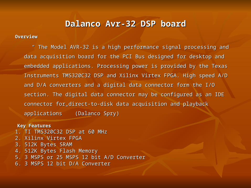
Dalanco Avr-32 DSP boardDalanco Avr-32 DSP board
OverviewOverview
“ “ The Model AVR-32 is a high performance signal processing and data acquisition board for The Model AVR-32 is a high performance signal processing and data acquisition board for
the PCI Bus designed for desktop and embedded applications. Processing power is provided the PCI Bus designed for desktop and embedded applications. Processing power is provided
by the Texas Instruments TMS320C32 DSP and Xilinx Virtex FPGA. High speed A/D and by the Texas Instruments TMS320C32 DSP and Xilinx Virtex FPGA. High speed A/D and
D/A converters and a digital data connector form the I/O section. The digital data connector D/A converters and a digital data connector form the I/O section. The digital data connector
may be configured as an IDE connector for direct-to-disk data acquisition and playback may be configured as an IDE connector for direct-to-disk data acquisition and playback
applications” (Dalanco Spry) applications” (Dalanco Spry)
Key FeaturesKey Features
1. TI TMS320C32 DSP at 60 MHz 1. TI TMS320C32 DSP at 60 MHz 2. Xilinx Virtex FPGA 2. Xilinx Virtex FPGA 3. 512K Bytes SRAM 3. 512K Bytes SRAM 4. 512K Bytes Flash Memory 4. 512K Bytes Flash Memory 5. 3 MSPS or 25 MSPS 12 bit A/D Converter 5. 3 MSPS or 25 MSPS 12 bit A/D Converter 6. 3 MSPS 12 bit D/A Converter 6. 3 MSPS 12 bit D/A Converter
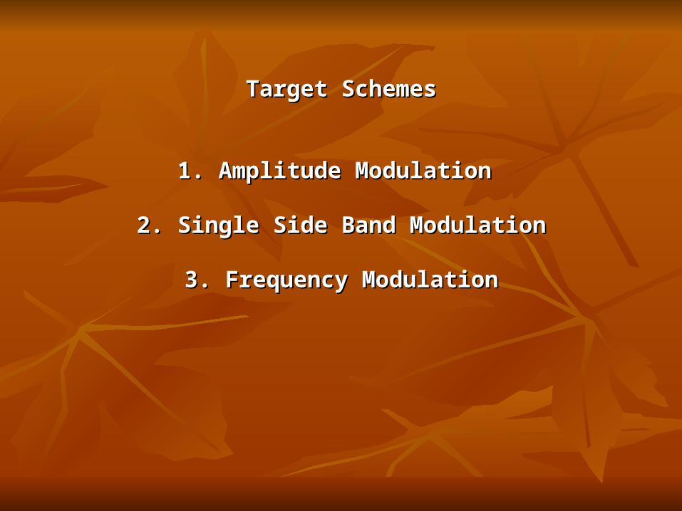
Target SchemesTarget Schemes
1. Amplitude Modulation 1. Amplitude Modulation
2. Single Side Band Modulation2. Single Side Band Modulation
3. Frequency Modulation3. Frequency Modulation
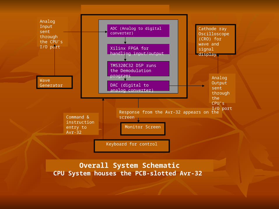
Analog Input sent through the CPU’s I/O port
Keyboard for control
Monitor Screen
Command & instruction entry to Avr-32
Response from the Avr-32 appears on the screen
Analog Output sent through the CPU’s I/O port
ADC (Analog to digital converter)
Xilinx FPGA for handling input/output
TMS320C32 DSP runs the Demodulation programs
DAC (digital to analog converter)
Cathode ray Oscilloscope (CRO) for wave and signal display
Wave Generator
Overall System SchematicCPU System houses the PCB-slotted Avr-32
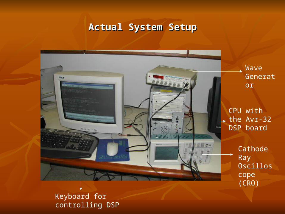
Actual System SetupActual System Setup
Wave Generator
Cathode Ray Oscilloscope (CRO)
Keyboard for controlling DSP
CPU with the Avr-32 DSP board
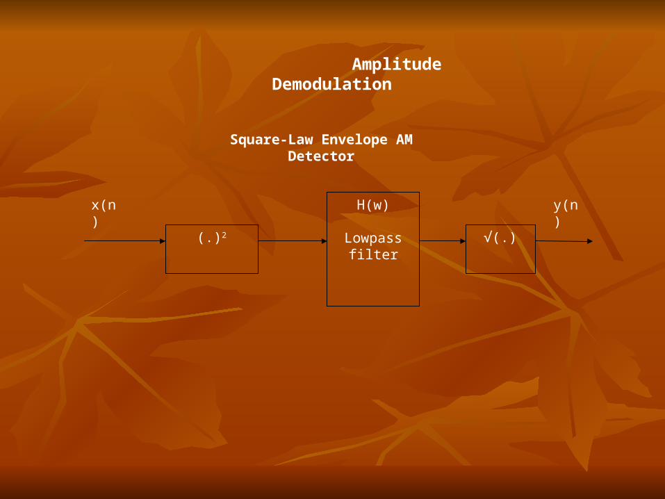
Amplitude Demodulation
H(w)
Lowpass filter
(.)2 √(.)
x(n) y(n)
Square-Law Envelope AM Detector
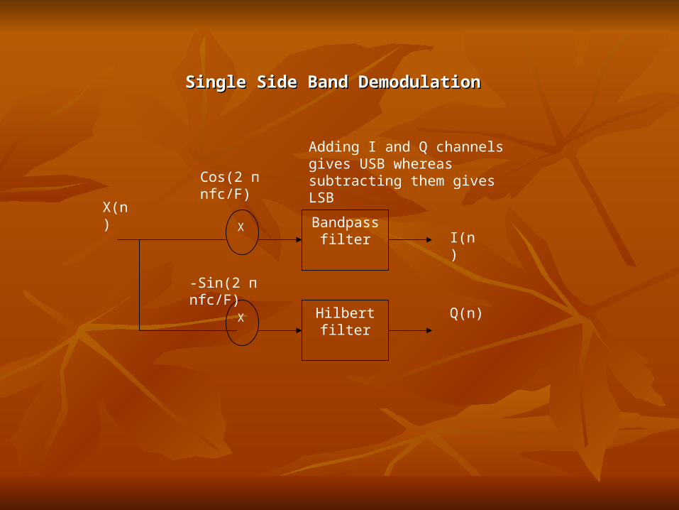
Single Side Band DemodulationSingle Side Band Demodulation
X
X
Bandpass filter
Hilbert filter
Cos(2 п nfc/F)
-Sin(2 п nfc/F)
I(n)
Q(n)
Adding I and Q channels gives USB whereas subtracting them gives LSB
X(n)
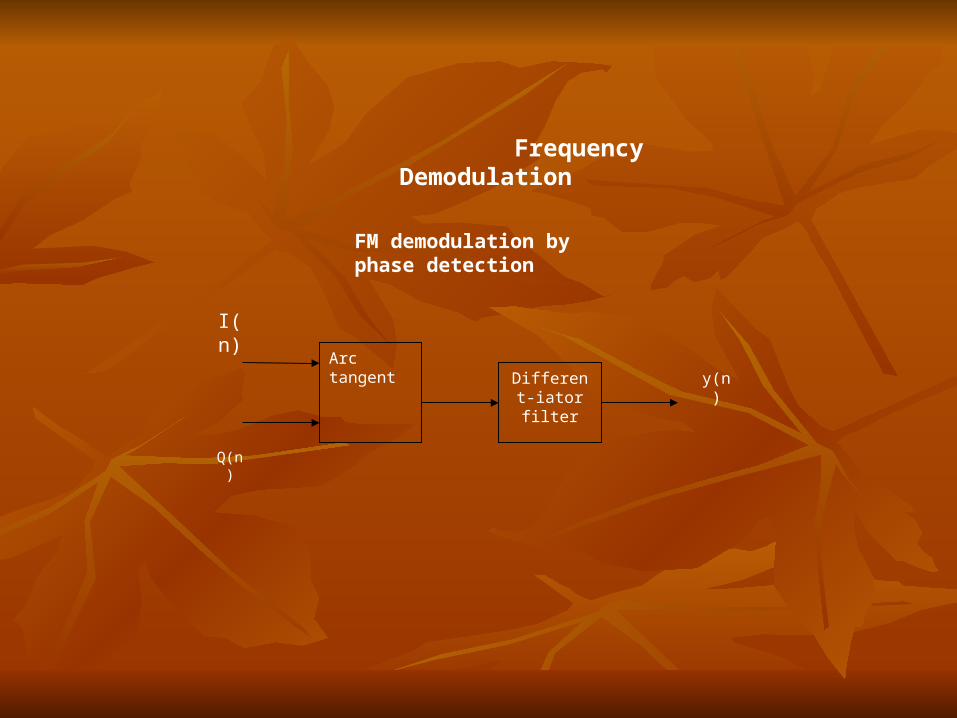
Frequency Demodulation
Different-iator filter
Arc tangent
I(n)
Q(n)
y(n)
FM demodulation by phase detection
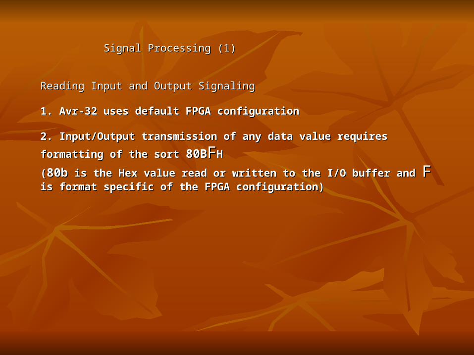
Signal Processing (1) Signal Processing (1)
Reading Input and Output SignalingReading Input and Output Signaling
1. Avr-32 uses default FPGA configuration1. Avr-32 uses default FPGA configuration
2. Input/Output transmission of any data value requires formatting of the sort 2. Input/Output transmission of any data value requires formatting of the sort 80B80BFFHH
((80b80b is the Hex value read or written to the I/O buffer and is the Hex value read or written to the I/O buffer and F F is format specific of the is format specific of the FPGA configuration)FPGA configuration)
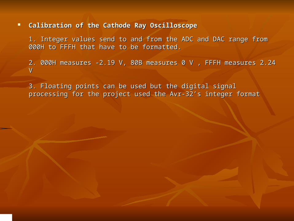
Calibration of the Cathode Ray OscilloscopeCalibration of the Cathode Ray Oscilloscope
1. Integer values send to and from the ADC and DAC range from 000H to FFFH that have to 1. Integer values send to and from the ADC and DAC range from 000H to FFFH that have to be formatted.be formatted.
2. 000H measures -2.19 V, 80B measures 0 V , FFFH measures 2.24 V2. 000H measures -2.19 V, 80B measures 0 V , FFFH measures 2.24 V
3. Floating points can be used but the digital signal processing for the project used the Avr-3. Floating points can be used but the digital signal processing for the project used the Avr-32’s integer format32’s integer format
25 inputmemorylocations used in producing every output. This time it is y[3].
Maximum address for input storage
Signal Processing (2)Signal Processing (2)
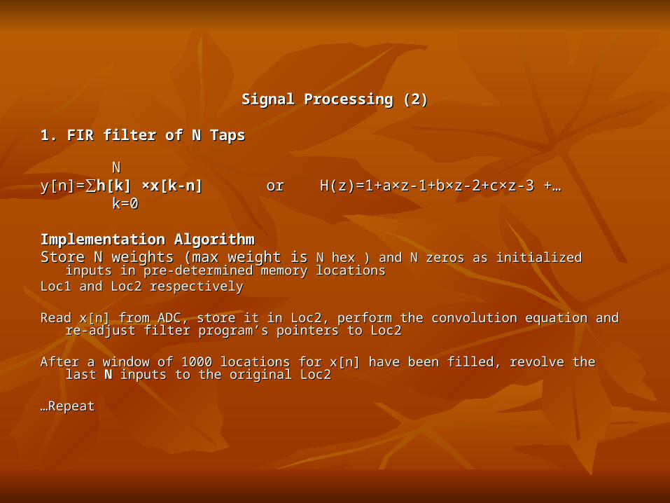
1. FIR filter of N Taps 1. FIR filter of N Taps
NNy[n]=y[n]=∑h[k] ×x[k-n]∑h[k] ×x[k-n] or H(z)=1+a×z-1+b×z-2+c×z-3 +… or H(z)=1+a×z-1+b×z-2+c×z-3 +… k=0k=0
Implementation AlgorithmImplementation AlgorithmStore N weights (max weight isStore N weights (max weight is N hex ) and N zeros as initialized inputs in pre-determined memory N hex ) and N zeros as initialized inputs in pre-determined memory
locationslocationsLoc1 and Loc2 respectivelyLoc1 and Loc2 respectively
Read x[n] from ADC, store it in Loc2, perform the convolution equation and re-adjust filter program’s pointers Read x[n] from ADC, store it in Loc2, perform the convolution equation and re-adjust filter program’s pointers to Loc2to Loc2
After a window of 1000 locations for x[n] have been filled, revolve the last After a window of 1000 locations for x[n] have been filled, revolve the last NN inputs to the original Loc2 inputs to the original Loc2
……RepeatRepeat
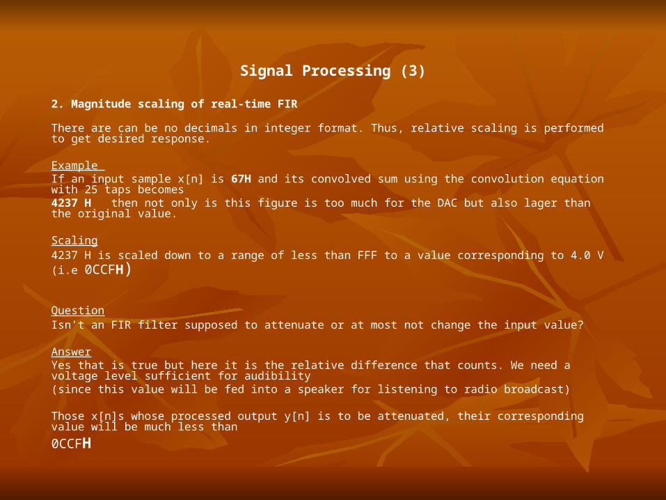
Signal Processing (3)
2. Magnitude scaling of real-time FIR
There are can be no decimals in integer format. Thus, relative scaling is performed to get desired response.
Example If an input sample x[n] is 67H and its convolved sum using the convolution equation with 25 taps becomes4237 H then not only is this figure is too much for the DAC but also lager than the original value.
Scaling
4237 H is scaled down to a range of less than FFF to a value corresponding to 4.0 V (i.e 0CCFH)
Question Isn’t an FIR filter supposed to attenuate or at most not change the input value?
AnswerYes that is true but here it is the relative difference that counts. We need a voltage level sufficient for audibility(since this value will be fed into a speaker for listening to radio broadcast)
Those x[n]s whose processed output y[n] is to be attenuated, their corresponding value will be much less than
0CCFH
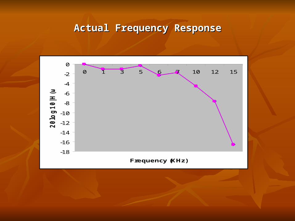
Actual Frequency ResponseActual Frequency Response
-18
-16
-14
-12
-10
-8
-6
-4
-2
0
0 1 3 5 6 7 10 12 15
Frequency (KHz)
20lo
g10|H
(ω)|
dB
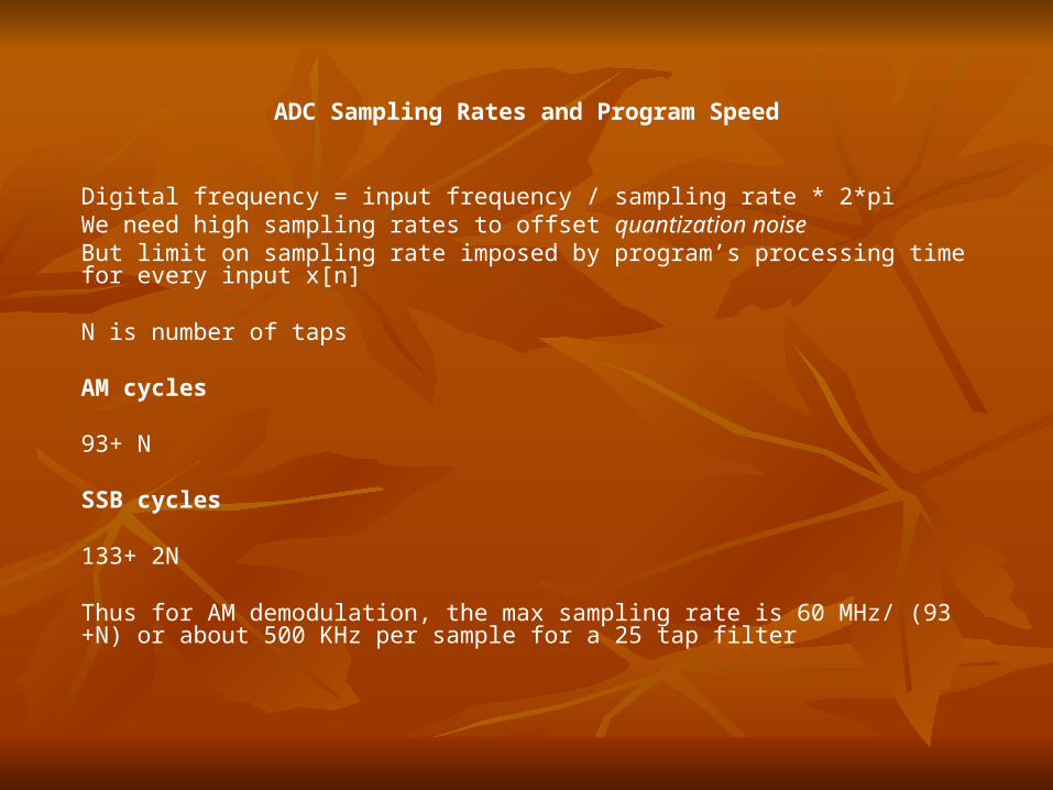
ADC Sampling Rates and Program Speed
Digital frequency = input frequency / sampling rate * 2*pi We need high sampling rates to offset quantization noise But limit on sampling rate imposed by program’s processing time for every input x[n]
N is number of taps
AM cycles
93+ N
SSB cycles
133+ 2N
Thus for AM demodulation, the max sampling rate is 60 MHz/ (93 +N) or about 500 KHz per sample for a 25 tap filter
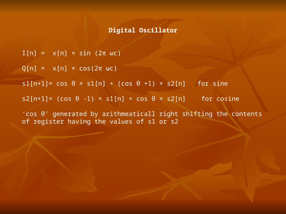
Digital Oscillator
I[n] = x[n] × sin (2π ωc)
Q[n] = x[n] × cos(2π ωc)
s1[n+1]= cos θ × s1[n] + (cos θ +1) × s2[n] for sine
s2[n+1]= (cos θ -1) × s1[n] + cos θ × s2[n] for cosine
‘cos θ’ generated by arithmeaticall right shifting the contents of register having the values of s1 or s2
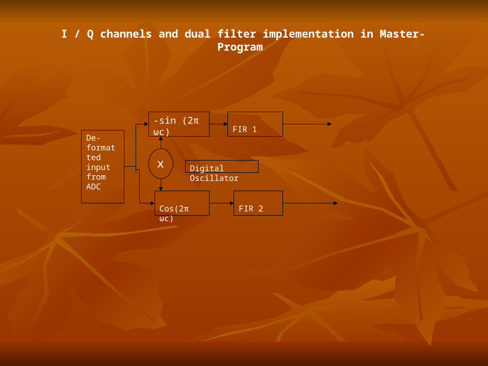
I / Q channels and dual filter implementation in Master-Program
-sin (2π ωc)
Cos(2π ωc)
FIR 1
FIR 2
x Digital Oscillator
De-formatted input from ADC
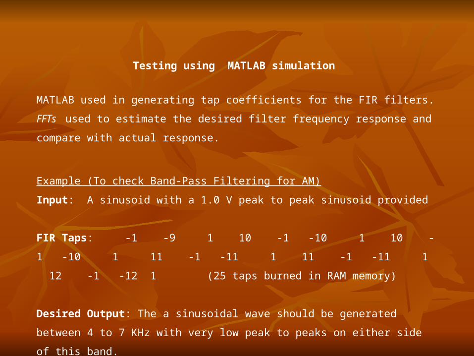
Testing using MATLAB simulation
MATLAB used in generating tap coefficients for the FIR filters. FFTs used to estimate
the desired filter frequency response and compare with actual response.
Example (To check Band-Pass Filtering for AM)
Input: A sinusoid with a 1.0 V peak to peak sinusoid provided
FIR Taps: -1 -9 1 10 -1 -10 1 10 -1 -10 1 11 -1 -11 1
11 -1 -11 1 12 -1 -12 1 (25 taps burned in RAM memory)
Desired Output: The a sinusoidal wave should be generated between 4 to 7 KHz with
very low peak to peaks on either side of this band.
Test Output: Band-pass range of 5.1 and 8.4 KHz and low peak to peaks on either
side
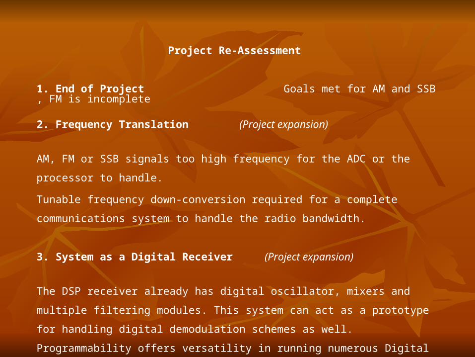
Project Re-Assessment
1. End of Project Goals met for AM and SSB , FM is incomplete
2. Frequency Translation (Project expansion)
AM, FM or SSB signals too high frequency for the ADC or the processor to handle.
Tunable frequency down-conversion required for a complete communications system
to handle the radio bandwidth.
3. System as a Digital Receiver (Project expansion)
The DSP receiver already has digital oscillator, mixers and multiple filtering modules.
This system can act as a prototype for handling digital demodulation schemes as well.
Programmability offers versatility in running numerous Digital and of course analog
schemes
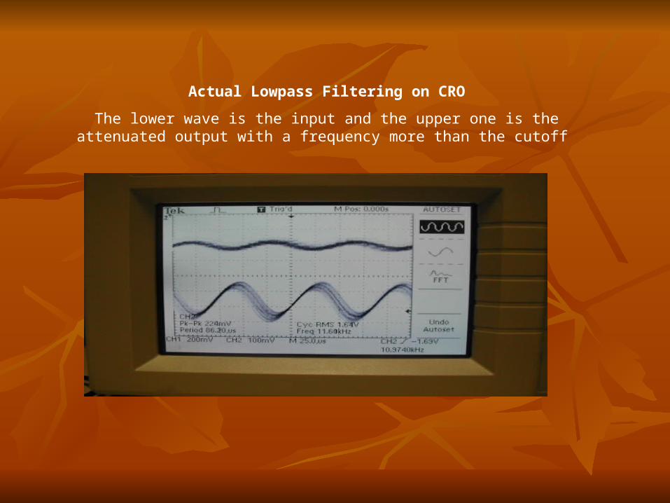
Actual Lowpass Filtering on CRO
The lower wave is the input and the upper one is the attenuated output with a frequency more than the cutoff
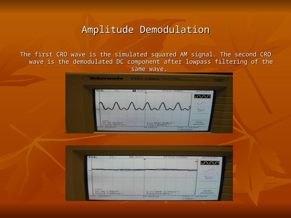
Amplitude DemodulationAmplitude Demodulation
The first CRO wave is the simulated squared AM signal. The second CRO wave is the The first CRO wave is the simulated squared AM signal. The second CRO wave is the demodulated DC component after lowpass filtering of the same wave. demodulated DC component after lowpass filtering of the same wave.
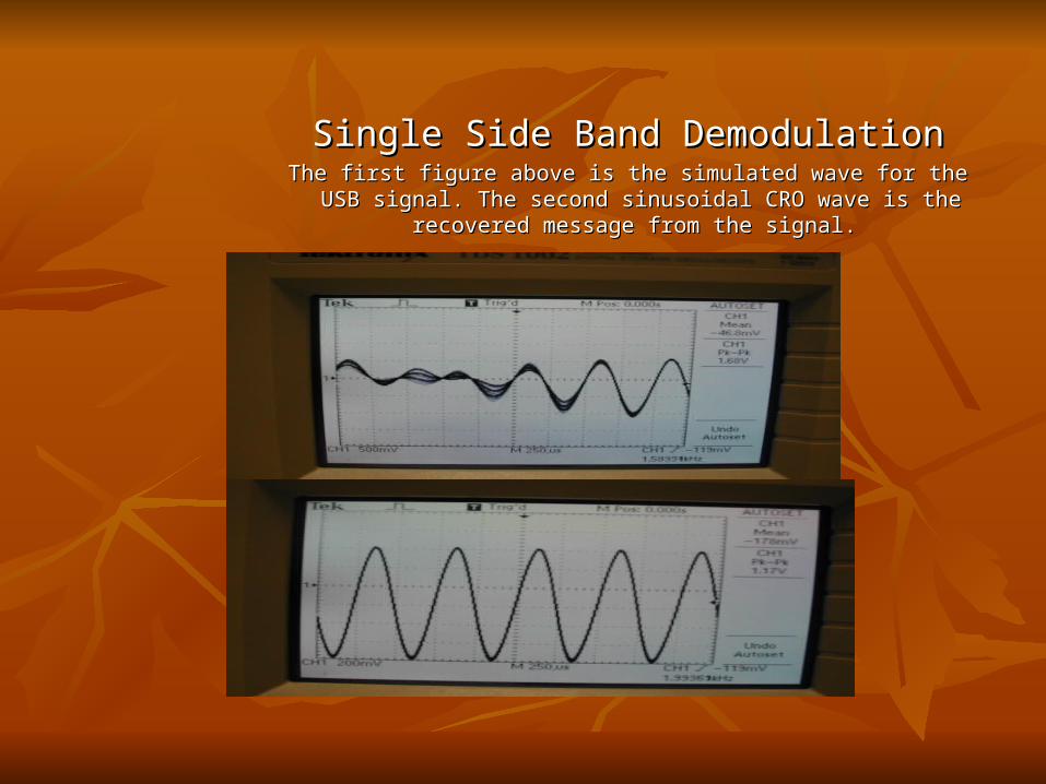
Single Side Band DemodulationSingle Side Band DemodulationThe first figure above is the simulated wave for the USB signal. The The first figure above is the simulated wave for the USB signal. The
second sinusoidal CRO wave is the recovered message from the second sinusoidal CRO wave is the recovered message from the signal.signal.
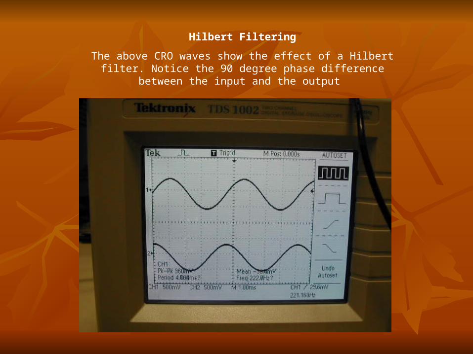
Hilbert Filtering
The above CRO waves show the effect of a Hilbert filter. Notice the 90 degree phase difference between the input and the output

Finished!
Related Documents