High speed FPGA based scalable parallel demodulator design Master’s Thesis by H.M. (Mark) Beekhof Committee: prof.dr.ir. M.J.G. Bekooij (CAES) dr.ir. A.B.J. Kokkeler (CAES) ir. J. Scholten (PS) G. Kuiper, M.Sc (CAES) University of Twente, Enschede, The Netherlands April 10, 2017

Welcome message from author
This document is posted to help you gain knowledge. Please leave a comment to let me know what you think about it! Share it to your friends and learn new things together.
Transcript
High speed FPGA based scalable parallel
demodulator design
Master’s Thesisby
H.M. (Mark) Beekhof
Committee:prof.dr.ir. M.J.G. Bekooij (CAES)
dr.ir. A.B.J. Kokkeler (CAES)ir. J. Scholten (PS)
G. Kuiper, M.Sc (CAES)
University of Twente, Enschede, The NetherlandsApril 10, 2017


Abstract
i
ii ABSTRACT
Nowadays applications have to process data at high data rates. These datarates are increasing faster than the frequencies on which Field ProgrammableGate Arrays (FPGAs) operates. In this thesis a parallel design is presentedso that the FPGA still can be useful to process data at high rates.
At the CAES group a ML605 FPGA evaluation board is available which isinterfaced with an Analog to Digital Converter (ADC). On this FPGA boarda multiprocessor system is installed named Starburst. It is possible to createhardware accelerators and integrate them into this system. An Universal Soft-ware Radio Peripheral (USRP) box is available, combined with the GNURadiosoftware it is possible to create a software defined radio.
First a reference conventional demodulator is created which processes thesamples in sequential order. The performance of this demodulator was testedusing GNURadio. The performance was tested by detecting packages at thereceiver side. The amount of packages combined with a certain level of noisethat was added resulted in a Packet Error Rate (PER) for different Signal toNoise Ratios (SNRs).
Thereafter, the design was implemented as a hardware accelerator on theFPGA. The performance of this implementation was compared to the onecreated using GNURadio. The performance, measured with the PER fordifferent SNRs, of the implementation on the FPGA was comparable with theone created in software for low SNRs. For high SNRs the implementation onthe FPGA has a certain floor in the PER.
After the reference conventional design was implemented a parallel designhas been created. The conventional design was a basis for this design. Theperformance of this design was compared to the conventional one. The per-formance was not as good as the conventional design. The design was lessrobust to a timing difference between the clocks of the transmitter and thereceiver. However, the reasons for this are explained in this report togetherwith possible solution directions. Due to time constraints it was not possibleto create an implementation that addresses the discussed issues. However itis expected that it is possible to create a parallel structure with an equal PERassuming no clock difference. However the design will be less robust to a clockdifference between transmitter and receiver. A disadvantage of the design isthat it will take up a lot of resources on the FPGA which will limit the amountof parallel paths that can be used. For the presented design, the maximumamount of parallel paths will be around 16, which is enough for the 5 GS/sADC that is available.
iii
As future work it would be interesting to implement the design in combina-tion with a high speed ADC that delivers samples in parallel. Further researchis required to improve the design so that it can be used in applications withother data rates.
Contents
Abstract i
1 Introduction 11.1 Context . . . . . . . . . . . . . . . . . . . . . . . . . . . . . . . 21.2 Problem Description . . . . . . . . . . . . . . . . . . . . . . . . 21.3 Related Work . . . . . . . . . . . . . . . . . . . . . . . . . . . . 31.4 Outline . . . . . . . . . . . . . . . . . . . . . . . . . . . . . . . 4
2 BPSK Basics 52.1 Phase Shift Keying . . . . . . . . . . . . . . . . . . . . . . . . . 6
2.1.1 BPSK . . . . . . . . . . . . . . . . . . . . . . . . . . . . 62.1.2 Non-Coherent versus Coherent . . . . . . . . . . . . . . 62.1.3 Performance . . . . . . . . . . . . . . . . . . . . . . . . 72.1.4 Implementation . . . . . . . . . . . . . . . . . . . . . . . 8
2.2 Modulation . . . . . . . . . . . . . . . . . . . . . . . . . . . . . 82.3 Demodulation . . . . . . . . . . . . . . . . . . . . . . . . . . . . 102.4 Symbol Time Recovery . . . . . . . . . . . . . . . . . . . . . . . 13
2.4.1 Early Late . . . . . . . . . . . . . . . . . . . . . . . . . 132.4.2 Gardner . . . . . . . . . . . . . . . . . . . . . . . . . . . 142.4.3 Mueller Muller . . . . . . . . . . . . . . . . . . . . . . . 14
2.5 Summary . . . . . . . . . . . . . . . . . . . . . . . . . . . . . . 15
3 Conventional DBPSK Demodulator 163.1 Design . . . . . . . . . . . . . . . . . . . . . . . . . . . . . . . . 17
3.1.1 Demodulation . . . . . . . . . . . . . . . . . . . . . . . . 173.1.2 Sampling . . . . . . . . . . . . . . . . . . . . . . . . . . 183.1.3 Top Level Design . . . . . . . . . . . . . . . . . . . . . . 23
3.2 Implementation . . . . . . . . . . . . . . . . . . . . . . . . . . . 253.2.1 GNURadio . . . . . . . . . . . . . . . . . . . . . . . . . 253.2.2 FPGA . . . . . . . . . . . . . . . . . . . . . . . . . . . . 26
3.3 Results . . . . . . . . . . . . . . . . . . . . . . . . . . . . . . . . 293.3.1 Set-up . . . . . . . . . . . . . . . . . . . . . . . . . . . . 293.3.2 PER . . . . . . . . . . . . . . . . . . . . . . . . . . . . . 293.3.3 Measurements . . . . . . . . . . . . . . . . . . . . . . . 30
iv
CONTENTS v
3.4 Summary . . . . . . . . . . . . . . . . . . . . . . . . . . . . . . 36
4 Parallel DBPSK Demodulator 374.1 Design . . . . . . . . . . . . . . . . . . . . . . . . . . . . . . . . 38
4.1.1 Switch . . . . . . . . . . . . . . . . . . . . . . . . . . . . 384.1.2 Demodulation . . . . . . . . . . . . . . . . . . . . . . . . 404.1.3 Symbol Time Recovery . . . . . . . . . . . . . . . . . . 41
4.2 Implementation . . . . . . . . . . . . . . . . . . . . . . . . . . . 424.2.1 Switch . . . . . . . . . . . . . . . . . . . . . . . . . . . . 434.2.2 Demodulation . . . . . . . . . . . . . . . . . . . . . . . . 444.2.3 Top Level Implementation . . . . . . . . . . . . . . . . . 44
4.3 Conclusion . . . . . . . . . . . . . . . . . . . . . . . . . . . . . 45
5 Results and Comparison 475.1 Results Parallel Receiver . . . . . . . . . . . . . . . . . . . . . . 485.2 Scalability . . . . . . . . . . . . . . . . . . . . . . . . . . . . . . 505.3 Alternative Parallel Structure . . . . . . . . . . . . . . . . . . . 535.4 Summary . . . . . . . . . . . . . . . . . . . . . . . . . . . . . . 53
6 Conclusion and Recommendations 556.1 Conclusion . . . . . . . . . . . . . . . . . . . . . . . . . . . . . 566.2 Recommendations . . . . . . . . . . . . . . . . . . . . . . . . . 57
List of Figures 59
Bibliography 63
Acronyms
ADC Analog to Digital Converter
BER Bit Error Rate
BPSK Binary Phase Shift Keying
DBPSK Differential Binary Phase Shift Keying
FIR Finite Impulse Response
FPGA Field Programmable Gate Array
I In-Phase
LUT Lookup Table
PER Packet Error Rate
PSK Phase Shift Keying
Q Quadrature
QAM Quadrature Amplitude Modulation
QBL-MSK Quasi-Bandlimited Minimum Shift Keying
QPSK Quadrature Phase Shift Keying
RAM Random Access Memory
ROM Read-only Memory
RF Radio Frequency
SNR Signal to Noise Ratio
SPS Samples per Symbol
TCXO Temperature Compensated Crystal Oscillator
USRP Universal Software Radio Peripheral
XOR Exclusive Or
CHAPTER 1Introduction
1
2 CHAPTER 1. INTRODUCTION
1.1 Context
The amount of data generated by applications is increasing. At NXP they areresearching the use of polymer waveguides in cars. These polymer waveguideshave several advantages over the cables that are used at the moment. One ofthe advantages is that it is possible to use higher data rates. These data ratesare higher than the clock frequency of currently available FPGAs. HoweverFPGAs can still be useful to process data. By processing data in parallel it ispossible to process data streams with a high data rate.
1.2 Problem Description
A high speed ADC is available which can read samples up to a rate of 5 GS/s.The maximum clock frequencies of FPGAs is currently much lower, thereforesamples should be processed in parallel. This ADC is not interfaced yet withthe multiprocessor system called Starburst, which is installed on the availableVirtex 6 FPGA board. Because it will cost a lot of time to interface theADC with the platform, a proof of concept will be created with an availableset-up. The set-up consists of a narrow band Radio Frequency (RF) receiverfrontend that has been interfaced with a Virtex 6 FPGA board such thatsoftware defined radio receiver applications can be prototyped on an embeddedmultiprocessor system. This set-up can be used to implement a referenceconventional demodulator and a parallel demodulator as a proof of concept.
The objective of this graduation project is the creation of a demodulatoron a FPGA which can process data at a rate of 5 GS/s where data is processedin parallel. This demodulator is implemented on a Virtex 6 FPGA which hasbeen interfaced with a RF receiver frontend. The demodulator should runon a lower frequency than the frequency at which the samples arrive. Theimplementation should be made such that it should be able to work with thehigh speed ADC. The implementation should be made scalable, so that it canbe used at higher data rates. To keep the demodulator simple Phase ShiftKeying (PSK) is used as modulation technique. Binary Phase Shift Keying(BPSK) is chosen because it is more suitable for the application in combi-nation with polymer waveguides. The reason is that these waveguides havea relatively high damping. BPSK will have a better performance under lowSNRs, from Bit Error Rate (BER) perspective, than higher order modulationschemes. The demodulator should be kept simple so that the focus is on cre-ating a parallel hardware structure. Design options should be explored andthe achieved performance of the system should be compared with theoreticalresults. This implementation should be scalable such that the same conceptcan be used to process samples of a high speed 5 GS/s ADC.
1.3. RELATED WORK 3
1.3 Related Work
There is some work done in the field of processing data in parallel in demodu-lators. In [13] a parallel demodulation structure is presented. This structure isbased on a frequency domain implementation of a matched filter. Besides thata Symbol-Timing Recovery Loop is discussed that uses an adapted version ofthe Gardner algorithm. This adapted version is suitable for implementationon an FPGA. The structure is tested with an uncoded BPSK signal. Simula-tion results show that their presented design is performing as well as the serialdesign.
In [4] a parallel demodulator structure suitable for implementation on aFPGA for a high order Quadrature Amplitude Modulation (QAM) signalis presented. An architecture is presented for a 5 GS/s demodulator of a64QAM signal. In this paper a symbol time recovery method was used thatwas presented in [7], which is not sensitive to SNR and carrier frequency offset.This timing recovery method is more complex but useful for QAM signals.
In [9] trade-offs for serial and parallel demodulation are discussed forQuasi-Bandlimited Minimum Shift Keying (QBL-MSK). The parallel imple-mentation in this case consists of 2 parallel paths, a In-Phase (I) and Quadra-ture (Q) path. This parallel structure is not useful because it does not runon a lower clock frequency than the rate at which the samples arrive. Twosynchronisation methods are used to for synchronisation. The first one is us-ing average zero crossing and the other one uses the maximum eye openingfor synchronisation. They conclude that zero crossing is providing either lessor the same BER degradation as that obtained with maximum eye openingsynchronisation. This is significant because zero crossing synchronisation isimplemented much easier in hardware.
In [20] a frequency-domain parallel demodulation structure is discussed. Inthis paper an improved structure is discussed which should be more useful inhigh speed systems. The timing synchronisation is combined with the matchedfilter. Because only the best points at the output of the matched filter areused for timing synchronisation. Simulation results are given for a system withQuadrature Phase Shift Keying (QPSK) modulation. They conclude that thestructure they presented is suitable for high-speed implementations.
All the related work above uses a frequency-domain parallel demodulationstructure. There was no related work found which uses a time-domain paralleldemodulation structure, except [9] where two time-domain parallel paths areused which do not run on a lower frequency. In the related work architecturesand algorithms were discussed for symbol time recovery which can be usefulfor the demodulator that is designed during this thesis.
4 CHAPTER 1. INTRODUCTION
1.4 Outline
First in Chapter 2 the basics of BPSK are discussed, which is necessary tounderstand the working of the BPSK demodulator. After that a conventionalDifferential Binary Phase Shift Keying (DBPSK) demodulator design andimplementation are discussed in Chapter 3. This conventional demodulatoris created so that it is possible to compare the performance of the parallelimplementation with a conventional implementation. The design of the con-ventional demodulator is used as a basis to design a parallel demodulationstructure which is discussed in Chapter 4. In Chapter 5 the results of themeasurements of both designs are compared with each other. Besides thatthere is a section about the scalability of the parallel design in this chapter.Chapter 6 will conclude this thesis with a conclusion and recommendations.
CHAPTER 2BPSK Basics
5
6 CHAPTER 2. BPSK BASICS
In this chapter the modulation technique of BPSK will be discussed. Afterwhich other demodulation techniques are discussed. A demodulation tech-nique will be chosen which is used in the rest of this thesis.
2.1 Phase Shift Keying
PSK is a digital modulation technique where the information is modulated bychanging the phase of the carrier signal. Because it is a digital modulationtechnique the number of distinct phases that used is finite.
To demodulate a PSK signal the received signal can be compared to areference signal, this method is called coherent demodulation. In case there isno reference signal used the method is called non-coherent demodulation. Inthe last case the received signal should be compared with itself. Differentialmodulation should be used to be able to demodulate a signal with a non-coherent technique.
2.1.1 BPSK
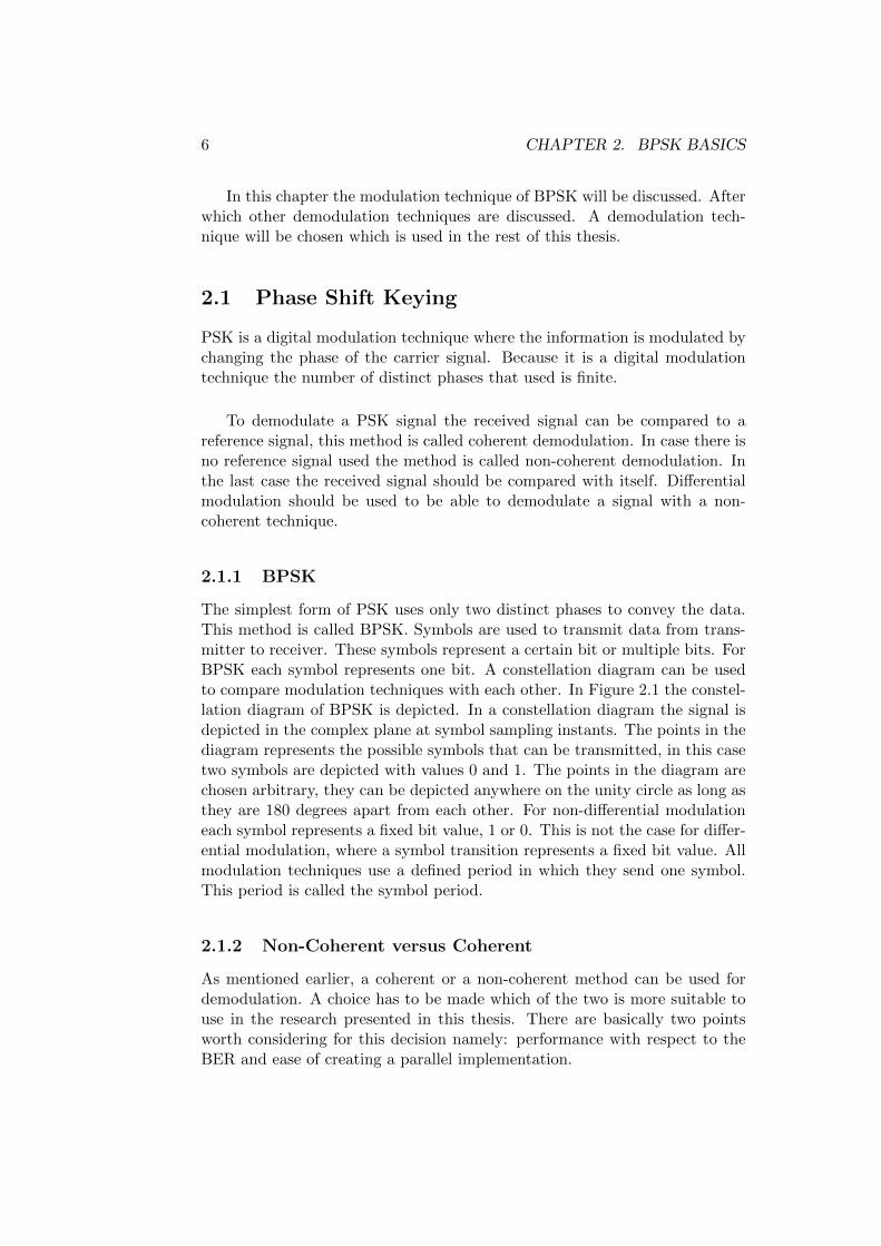
The simplest form of PSK uses only two distinct phases to convey the data.This method is called BPSK. Symbols are used to transmit data from trans-mitter to receiver. These symbols represent a certain bit or multiple bits. ForBPSK each symbol represents one bit. A constellation diagram can be usedto compare modulation techniques with each other. In Figure 2.1 the constel-lation diagram of BPSK is depicted. In a constellation diagram the signal isdepicted in the complex plane at symbol sampling instants. The points in thediagram represents the possible symbols that can be transmitted, in this casetwo symbols are depicted with values 0 and 1. The points in the diagram arechosen arbitrary, they can be depicted anywhere on the unity circle as long asthey are 180 degrees apart from each other. For non-differential modulationeach symbol represents a fixed bit value, 1 or 0. This is not the case for differ-ential modulation, where a symbol transition represents a fixed bit value. Allmodulation techniques use a defined period in which they send one symbol.This period is called the symbol period.
2.1.2 Non-Coherent versus Coherent
As mentioned earlier, a coherent or a non-coherent method can be used fordemodulation. A choice has to be made which of the two is more suitable touse in the research presented in this thesis. There are basically two pointsworth considering for this decision namely: performance with respect to theBER and ease of creating a parallel implementation.
2.1. PHASE SHIFT KEYING 7
Figure 2.1: Constellation Diagram of BPSK
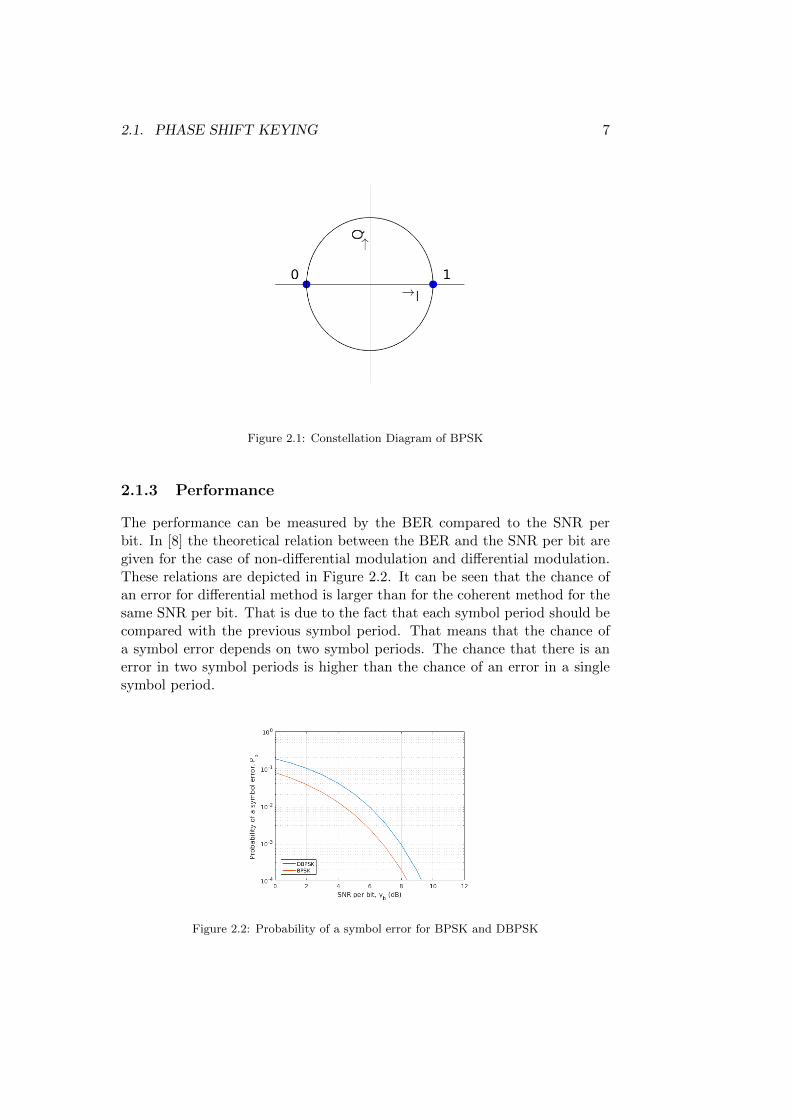
2.1.3 Performance
The performance can be measured by the BER compared to the SNR perbit. In [8] the theoretical relation between the BER and the SNR per bit aregiven for the case of non-differential modulation and differential modulation.These relations are depicted in Figure 2.2. It can be seen that the chance ofan error for differential method is larger than for the coherent method for thesame SNR per bit. That is due to the fact that each symbol period should becompared with the previous symbol period. That means that the chance ofa symbol error depends on two symbol periods. The chance that there is anerror in two symbol periods is higher than the chance of an error in a singlesymbol period.
Figure 2.2: Probability of a symbol error for BPSK and DBPSK
8 CHAPTER 2. BPSK BASICS
2.1.4 Implementation
As discussed before for non-coherent BPSK no reference signal is required atthe receiver because the info is encoded in changes of the phase. That meansthat no circuit is necessary to generate this reference signal. Therefore theimplementation of non-coherent BPSK can be less complex than the imple-mentation of a coherent demodulation technique. Assuming that creation ofthe reference signal is part of the demodulator, when that is the case thecircuit required to create the reference signal should be made parallel too.
Because the focus in this thesis is on parallelism in demodulators the non-coherent method is used. The reason therefore is that there is no referencesignal required at the receiver and therefore it is easier to create a parallelstructure, because there is no circuit required for the creation of the referencesignal. The degradation in BER is not problematic as long as the paralleldemodulator is compared with a demodulator that uses the same technique.In future designs it is possible to add a circuit to the design that creates thereference signal.
2.2 Modulation
Equation 2.1 can be used to modulate a signal using BPSK. Where x(n) isthe data signal consisting of bits and k is the sensitivity given by Equation 2.2where f0 is the frequency used and fs is the sampling frequency. x(n) shouldbe interpolated with the number of Samples per Symbol (SPS). SPS is thenumber of samples that is used to send one symbol it is equivalent to thesymbol period.
y(m) = cos(km+ π · x(n)
)(2.1)
k = 2πf0fs
(2.2)
To be able to demodulate without a reference signal the signal should bemodulated differential. To make the signal differential each bit should becompared with the previous bit, when they are the same x(n) should be 0otherwise it should be 1. This can be accomplished by using an Exclusive Or(XOR) of the current bit with the previous bit.
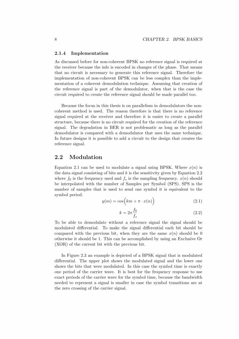
In Figure 2.3 an example is depicted of a BPSK signal that is modulateddifferential. The upper plot shows the modulated signal and the lower oneshows the bits that were modulated. In this case the symbol time is exactlyone period of the carrier wave. It is best for the frequency response to useexact periods of the carrier wave for the symbol time, because the bandwidthneeded to represent a signal is smaller in case the symbol transitions are atthe zero crossing of the carrier signal.
2.2. MODULATION 9
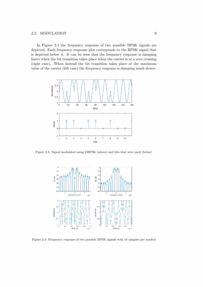
In Figure 2.4 the frequency response of two possible BPSK signals aredepicted. Each frequency response plot corresponds to the BPSK signal thatis depicted below it. It can be seen that the frequency response is dampingfaster when the bit transition takes place when the carrier is at a zero crossing(right case). When instead the bit transition takes place at the maximumvalue of the carrier (left case) the frequency response is damping much slower.
Figure 2.3: Signal modulated using DBPSK (above) and bits that were used (below)
Figure 2.4: Frequency response of two possible BPSK signals with 16 samples per symbol
10 CHAPTER 2. BPSK BASICS
2.3 Demodulation
It is possible to demodulate a DBPSK signal in time domain or in the fre-quency domain. In this thesis the focus is on the time domain demodulationof the signal. The reason therefore is that I have more knowledge with demod-ulating signals in time-domain. The demodulation of a BPSK signal startswith a mixing process to remove the carrier frequency out of the signal. Thiscan be done by multiplying the received signal with a cosine at the carrierfrequency. This demodulation step can be described mathematically. Themultiplication of two cosines can be rewritten using Equation 2.3. The resultis a sum of two cosines, one with the frequency difference and one with thesum of the two frequencies.
cos(α) · cos(β) =cos(α+ β) + cos(α− β)
2(2.3)
A simplified version of the received signal x(t) is given by Equation 2.4.Where m(t) is the modulation signal and ωc is the carrier frequency. To de-modulate the signal it can be multiplied with a signal at the same frequency,see Equation 2.5. This signal is either the reference signal for coherent de-modulation of a signal that is generated using the local oscillator in case ofnon-coherent demodulation. The result of this multiplication is given by Equa-tion 2.6. One part of the signal is now independent of the carrier frequency,this part is useful to further demodulate the signal. With a low-pass filter thehigh frequency part can be removed from the signal.
x(t) = cos(ωct+ πm(t)
)(2.4)
y(t) = x(t) · cos(ωct) (2.5)
y(t) =cos
(2ωct+ πm(t)
)+ cos
(πm(t)
)2
(2.6)
Assuming that an ideal low-pass filter is used, the result of the filteringprocess is given by Equation 2.7. It is known that m(t) contains only zerosand ones (the actual bits). This signal is multiplied with π within the cosine.The cosine of 0 and π is respectively 1 and -1. That means that y(t) containsdirectly the bits where a 0 is represented by a value of −1
2 and a 1 by 12 .
y(t) =1
2cos
(πm(t)
)(2.7)
So given that m(t) only takes values of 0 and 1, y(t) can be simplified to:
y(t) = −1
2|m(t) = 0 (2.8)
y(t) =1
2|m(t) = 1 (2.9)
2.3. DEMODULATION 11
Which means the signal is completed demodulation. Concluding the demod-ulation of a BPSK signal can be done with a mixer and a low-pass filter.This demodulation method is assuming that there is no phase or frequencydifference between the received and local signal.
When there is an unknown phase difference between the local signal andthe received signal another demodulation method should be used. Which is thecase for non-coherent demodulation. A second mixer should be added to thedemodulator. This second mixer should use a local signal that is orthogonalwith the other local signal. When x(t) has an unknown phase difference it isdescribed by Equation 2.10.
x(t) = cos(ωct+ πm(t) + φ
)(2.10)
where ωc is the carrier frequency, m(t) the modulation signal and φ the un-known phase. If the received signal is mixed with a cosine and sine separatelythe multiplication results are given by Equation 2.11 and 2.12. The result ofthe multiplication with a cosine will be referred to as the I component of thesignal. The result of the multiplication with a sine will be referred to as theQ component of the signal.
I(t) =cos
(2ωct+ πm(t) + φ
)+ cos
(πm(t) + φ
)2
(2.11)
Q(t) =sin
(2ωct+ πm(t) + φ
)+ sin
(πm(t) + φ
)2
(2.12)
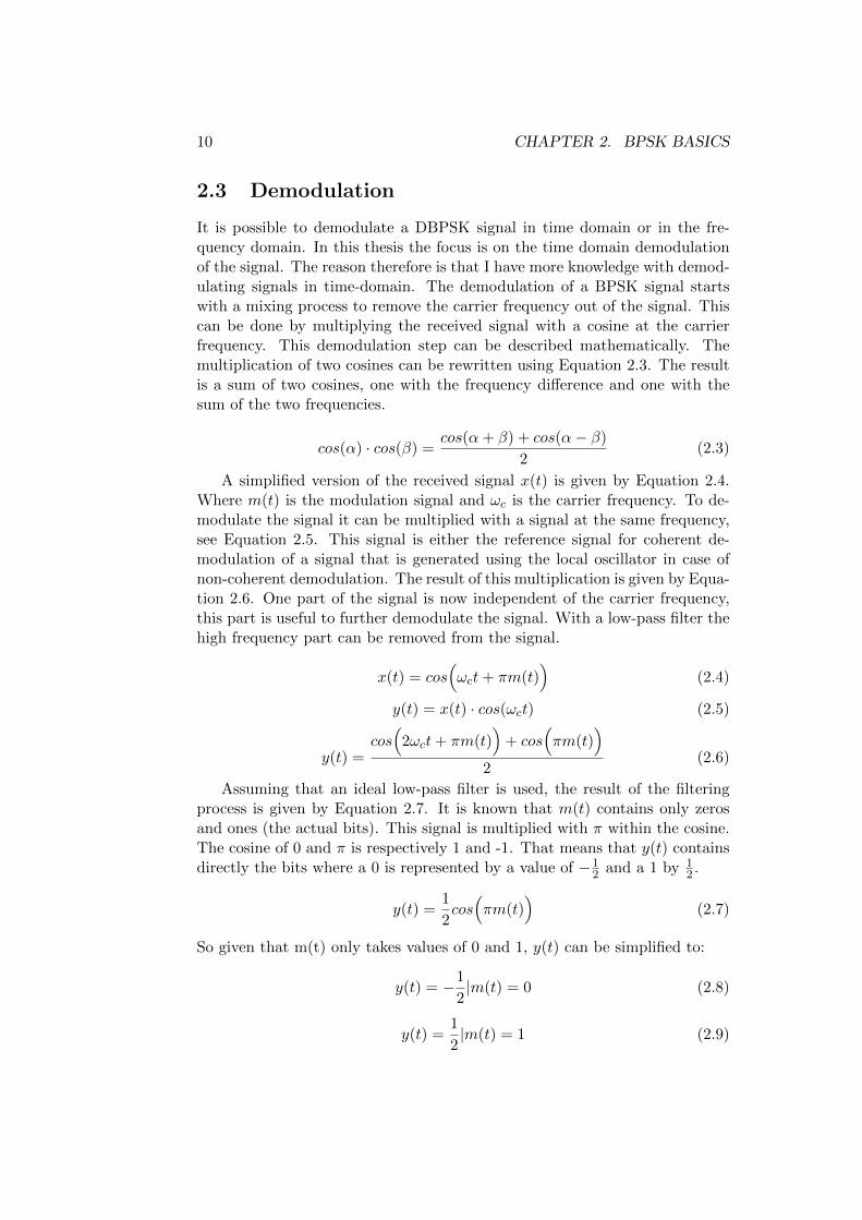
In Figure 2.5 the signals I(t) and Q(t) are depicted. In this case thereceived signal and the local generated signal at the receiver are in phase witheach other.
When both multiplication results are filtered with an ideal low-pass filterthe results become:
I(t) =1
2cos
(πm(t) + φ
)(2.13)
Q(t) =1
2sin
(πm(t) + φ
)(2.14)
12 CHAPTER 2. BPSK BASICS
Figure 2.5: Signals showing the bits that are modulated (a), modulated DBPSK signal (b),I component (c) and Q component (d) of the signal after mixing
Assuming that m(t) can only be 0 or 1 the results can be split up:
I(t) =1
2cos
(φ)|m(t) = 0 (2.15)
I(t) = −1
2cos
(φ)|m(t) = 1 (2.16)
Q(t) =1
2sin
(φ)|m(t) = 0 (2.17)
Q(t) = −1
2sin
(φ)|m(t) = 1 (2.18)
Now there are two signals (I(t) and Q(t)) that both contain a part ofthe modulated signal. It depends on the phase difference how the signal isdivided over these two signals. When the received signal and the local signalare in phase, I(t) will contain all information. When they are 90 degrees outof phase all information will be in Q(t). If the phase difference is somewherein between the information is divided over I(t) and Q(t). For non-coherentdemodulation it is not known if the signals are in phase or not.
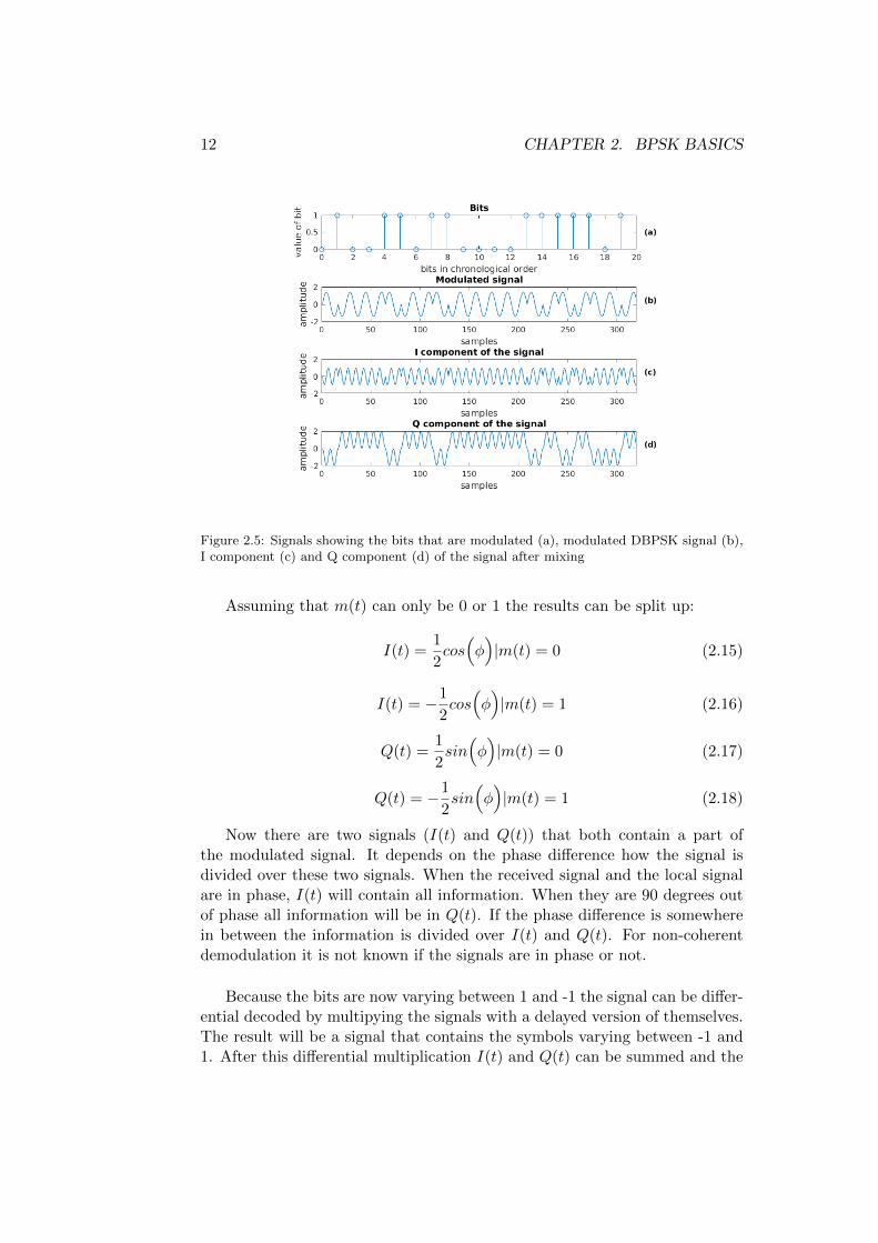
Because the bits are now varying between 1 and -1 the signal can be differ-ential decoded by multipying the signals with a delayed version of themselves.The result will be a signal that contains the symbols varying between -1 and1. After this differential multiplication I(t) and Q(t) can be summed and the
2.4. SYMBOL TIME RECOVERY 13
result is the completely demodulated signal. In Figure 2.6 the resulting sig-nals are depicted. The last signal is the demodulated signal. When this signalis sampled at the right sample moments the bits can be recovered. How theright sampling moment is determined will be explained in the next section.
Figure 2.6: Signals showing respectively the filtered I and Q component of the signal, dif-ferential I and Q signal and the sum of both differential signals.
2.4 Symbol Time Recovery
In the previous sections it was mentioned that the signal should be sampledat the right sampling moments. When the signal is not sampled at the rightmoments the change of an error increases. When the worst sampling momentis used the signal is completely lost. For non-coherent demodulation to get thecorrect sample moments the demodulator should include a symbol recoveringalgorithm. A few possible algorithms are discussed below. The discussedalgorithms are algorithms consisting of simple operations so that they aresuitable for implementation on an FPGA.
2.4.1 Early Late
The timing recovery consists of an error function to estimate the error thatwas made. The error is passed through a loop filter to get the right values thatare necessary to correct the timing error. There are a lot of error functionsthat can be used, one is the early late algorithm [5]. The error function is given
14 CHAPTER 2. BPSK BASICS
by Equation 2.19. There are three samples per symbol used to estimate theerror, one just before the actual sample and one just after the actual sample.
e(n) =(x[nT + Ts]− x[nT − Ts]
)x[nT ] (2.19)
where e(n) is the error function at sample moment n, x(n) is the oversampleddemodulated signal at sample moment n, T is the symbol period and Ts issmaller or equal to halve the symbol period.
2.4.2 Gardner
Another algorithm is the Gardner algorithm [3], of which a simplified versionis also used in [13]. The error function for the Gardner algorithm is given byEquation 2.20. Where e(n) is the error for sample n. For each symbol twosamples are required to estimate the error. One at the optimal sampling timeand one halfway the symbol period.
e(n) =(x[nT ]− x[(n− 1)T ]
)x[nT − T/2] (2.20)
where e(n) is the error function at sample moment n, x(n) is the oversampleddemodulated signal at sample moment n and T is the symbol period.
2.4.3 Mueller Muller
The algorithm that uses the least samples per symbol is the Mueller MullerAlgorithm [6]. The error function for this algorithm is given by Equation 2.21.The hat indicates the symbol decision that was at that sampling instance.Advantage of this algorithm is that it only needs 1 sample per symbol. Thiswill in turn result in less robustness of the symbol recovery.
e(n) =(x[nT ]x[(n− 1)T ]
)−(x[nT ]x[(n− 1)T ]
)(2.21)
where e(n) is the error function at sample moment n, x(n) is the oversampleddemodulated signal at sample moment n and T is the symbol period.
All of the above discussed algorithms need bit transitions to be able tofind the right sampling moment. Besides that the algorithm needs a certaintime amount for finding the right sample moment. Therefore the first bitsthat were transmitted will have a higher change of error. When a constantstream of bits will be transmitted this will not be a problem. However whenthere are a lots of zeros or ones in a burst this can become a problem. Whichwill result in less robustness against a clock difference.
2.5. SUMMARY 15
2.5 Summary
In this chapter the choice for BPSK was discussed. After that, the differencebetween coherent and non-coherent was made clear. Thereafter, the basicsof modulation and demodulation for BPSK were explained. DBPSK mod-ulation is chosen because it is simpler to implement and that technique iseasier to create a parallel structure for. Because I have more knowledge abouttime domain demodulation that one is used in the demodulator instead of fre-quency domain demodulation. Three symbol time recovering algorithms werediscussed and their importance in the demodulation process.
CHAPTER 3Conventional DBPSK
Demodulator
16
3.1. DESIGN 17
In the previous chapter the basic principals of the demodulation techniquefor BPSK were discussed. In this chapter the actual design of a sequentialDBPSK demodulator is discussed. Sequential means that the samples areprocessed one after each other in the order that they arrive at the demodulator.In this thesis we refer to this design as the conventional design. After that theGNURadio software is discussed and the implementation of the demodulatorin this software. Thereafter the implementation on the FPGA is discussed.The set-up used for the measurements is clarified after that. Finally somemeasurement results are discussed. This whole chapter will be a basis for ourparallel DBPSK demodulator design.
3.1 Design
As discussed earlier it is possible to demodulate the signal in the time do-main as well as in the frequency domain. We have chosen for a time domainimplementation because there is more personal experience with this implemen-tation. The focus in this thesis is on parallelising a demodulator, therefore itis best to implement a well known demodulation process. Besides that there ismore knowledge and information available about time domain demodulation.The design is roughly split in two parts, known as the demodulation part andthe sampling part. First the demodulation part will be discussed after whichthe symbol recovery part will be discussed. At last in this section the top leveldesign which combines these two parts will be discussed.
3.1.1 Demodulation
A demodulator consists of a mixer and a low-pass filter. In the created designa differential demodulation technique is used. A demodulation structure wascreated which was discussed in [8]. This structure uses an I and Q path todemodulate the signal. These paths are created by multiplying the receivedsignal with a cosine and a sine at the carrier frequency. Both paths are filteredwith a moving average filter. Both paths contain a differential multiplier thatis used to multiply a delayed version of the signal with the signal. In thisway it can be determined if there was a transition in the signal from positiveto negative, from negative to positive or that there was no transition. Thesignals can be added together after this multiplier.
As discussed the received signal should be multiplied with a sine and cosinewhich are generated at the receiver side with a local oscillator. In Figure 3.1the block scheme of a part of the demodulator is depicted, this block is referredto as the ”demod block”. It was chosen to create the block in this way so thatthe same block can be used for both the I and Q demodulation path. Theinputs are the received signal and a local signal. This local signal should be
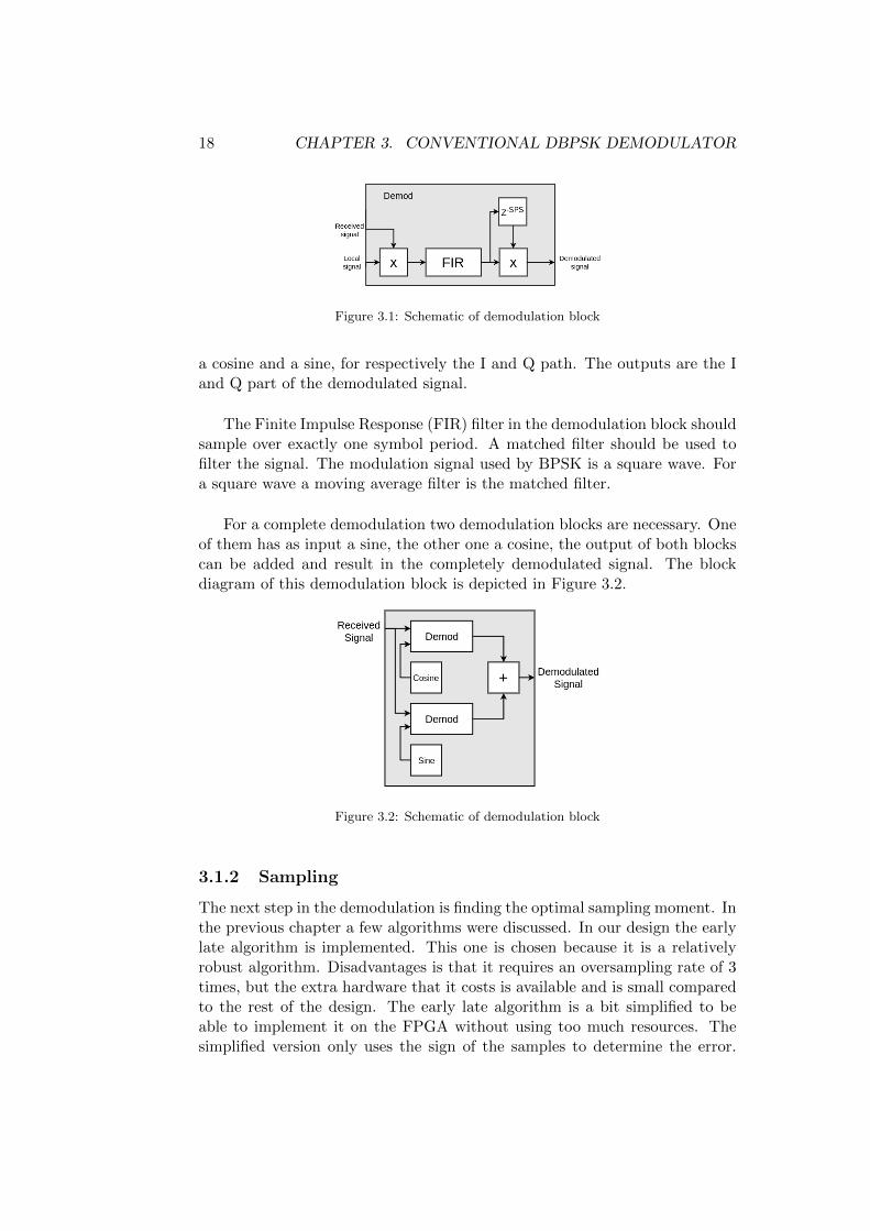
18 CHAPTER 3. CONVENTIONAL DBPSK DEMODULATOR
Figure 3.1: Schematic of demodulation block
a cosine and a sine, for respectively the I and Q path. The outputs are the Iand Q part of the demodulated signal.
The Finite Impulse Response (FIR) filter in the demodulation block shouldsample over exactly one symbol period. A matched filter should be used tofilter the signal. The modulation signal used by BPSK is a square wave. Fora square wave a moving average filter is the matched filter.
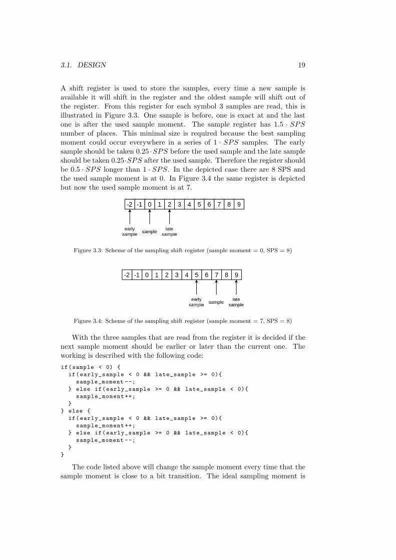
For a complete demodulation two demodulation blocks are necessary. Oneof them has as input a sine, the other one a cosine, the output of both blockscan be added and result in the completely demodulated signal. The blockdiagram of this demodulation block is depicted in Figure 3.2.
Figure 3.2: Schematic of demodulation block
3.1.2 Sampling
The next step in the demodulation is finding the optimal sampling moment. Inthe previous chapter a few algorithms were discussed. In our design the earlylate algorithm is implemented. This one is chosen because it is a relativelyrobust algorithm. Disadvantages is that it requires an oversampling rate of 3times, but the extra hardware that it costs is available and is small comparedto the rest of the design. The early late algorithm is a bit simplified to beable to implement it on the FPGA without using too much resources. Thesimplified version only uses the sign of the samples to determine the error.
3.1. DESIGN 19
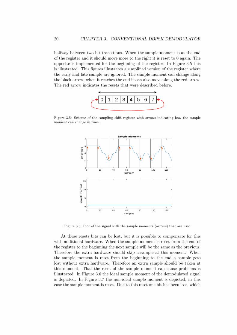
A shift register is used to store the samples, every time a new sample isavailable it will shift in the register and the oldest sample will shift out ofthe register. From this register for each symbol 3 samples are read, this isillustrated in Figure 3.3. One sample is before, one is exact at and the lastone is after the used sample moment. The sample register has 1.5 · SPSnumber of places. This minimal size is required because the best samplingmoment could occur everywhere in a series of 1 · SPS samples. The earlysample should be taken 0.25 ·SPS before the used sample and the late sampleshould be taken 0.25·SPS after the used sample. Therefore the register shouldbe 0.5 · SPS longer than 1 · SPS. In the depicted case there are 8 SPS andthe used sample moment is at 0. In Figure 3.4 the same register is depictedbut now the used sample moment is at 7.
Figure 3.3: Scheme of the sampling shift register (sample moment = 0, SPS = 8)
Figure 3.4: Scheme of the sampling shift register (sample moment = 7, SPS = 8)
With the three samples that are read from the register it is decided if thenext sample moment should be earlier or later than the current one. Theworking is described with the following code:
if(sample < 0) {
if(early_sample < 0 && late_sample >= 0){
sample_moment --;
} else if(early_sample >= 0 && late_sample < 0){
sample_moment ++;
}
} else {
if(early_sample < 0 && late_sample >= 0){
sample_moment ++;
} else if(early_sample >= 0 && late_sample < 0){
sample_moment --;
}
}
The code listed above will change the sample moment every time that thesample moment is close to a bit transition. The ideal sampling moment is
20 CHAPTER 3. CONVENTIONAL DBPSK DEMODULATOR
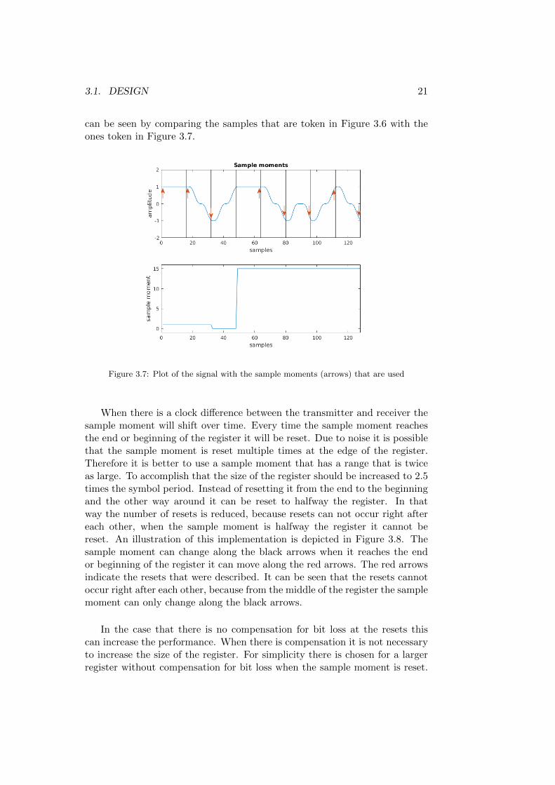
halfway between two bit transitions. When the sample moment is at the endof the register and it should move more to the right it is reset to 0 again. Theopposite is implemented for the beginning of the register. In Figure 3.5 thisis illustrated. This figures illustrates a simplified version of the register wherethe early and late sample are ignored. The sample moment can change alongthe black arrow, when it reaches the end it can also move along the red arrow.The red arrow indicates the resets that were described before.
Figure 3.5: Scheme of the sampling shift register with arrows indicating how the samplemoment can change in time
Figure 3.6: Plot of the signal with the sample moments (arrows) that are used
At these resets bits can be lost, but it is possible to compensate for thiswith additional hardware. When the sample moment is reset from the end ofthe register to the beginning the next sample will be the same as the previous.Therefore the extra hardware should skip a sample at this moment. Whenthe sample moment is reset from the beginning to the end a sample getslost without extra hardware. Therefore an extra sample should be taken atthis moment. That the reset of the sample moment can cause problems isillustrated. In Figure 3.6 the ideal sample moment of the demodulated signalis depicted. In Figure 3.7 the non-ideal sample moment is depicted, in thiscase the sample moment is reset. Due to this reset one bit has been lost, which
3.1. DESIGN 21
can be seen by comparing the samples that are token in Figure 3.6 with theones token in Figure 3.7.
Figure 3.7: Plot of the signal with the sample moments (arrows) that are used
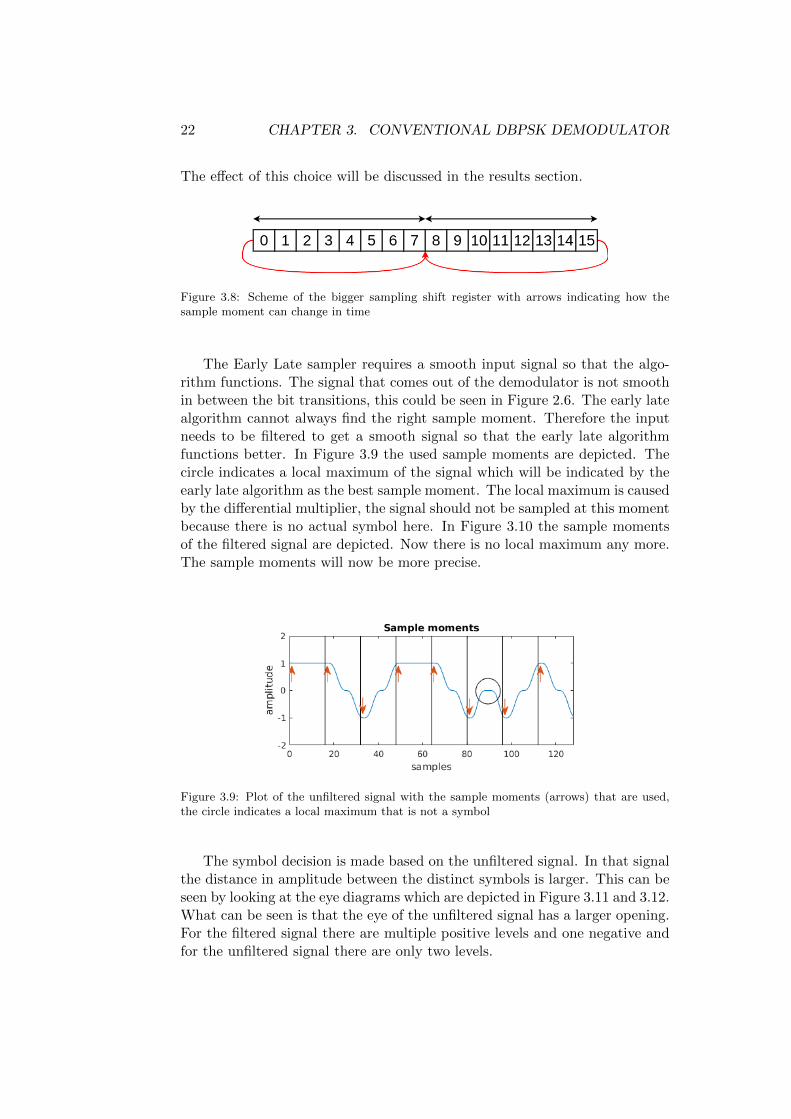
When there is a clock difference between the transmitter and receiver thesample moment will shift over time. Every time the sample moment reachesthe end or beginning of the register it will be reset. Due to noise it is possiblethat the sample moment is reset multiple times at the edge of the register.Therefore it is better to use a sample moment that has a range that is twiceas large. To accomplish that the size of the register should be increased to 2.5times the symbol period. Instead of resetting it from the end to the beginningand the other way around it can be reset to halfway the register. In thatway the number of resets is reduced, because resets can not occur right aftereach other, when the sample moment is halfway the register it cannot bereset. An illustration of this implementation is depicted in Figure 3.8. Thesample moment can change along the black arrows when it reaches the endor beginning of the register it can move along the red arrows. The red arrowsindicate the resets that were described. It can be seen that the resets cannotoccur right after each other, because from the middle of the register the samplemoment can only change along the black arrows.
In the case that there is no compensation for bit loss at the resets thiscan increase the performance. When there is compensation it is not necessaryto increase the size of the register. For simplicity there is chosen for a largerregister without compensation for bit loss when the sample moment is reset.
22 CHAPTER 3. CONVENTIONAL DBPSK DEMODULATOR
The effect of this choice will be discussed in the results section.
Figure 3.8: Scheme of the bigger sampling shift register with arrows indicating how thesample moment can change in time
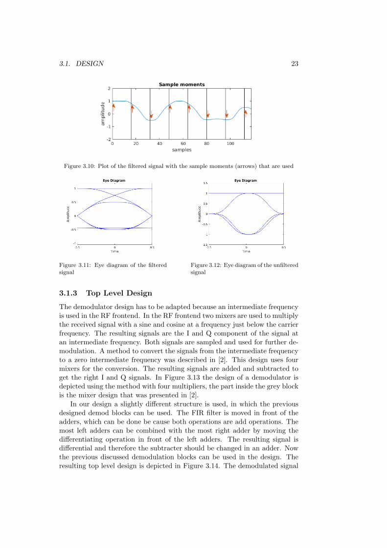
The Early Late sampler requires a smooth input signal so that the algo-rithm functions. The signal that comes out of the demodulator is not smoothin between the bit transitions, this could be seen in Figure 2.6. The early latealgorithm cannot always find the right sample moment. Therefore the inputneeds to be filtered to get a smooth signal so that the early late algorithmfunctions better. In Figure 3.9 the used sample moments are depicted. Thecircle indicates a local maximum of the signal which will be indicated by theearly late algorithm as the best sample moment. The local maximum is causedby the differential multiplier, the signal should not be sampled at this momentbecause there is no actual symbol here. In Figure 3.10 the sample momentsof the filtered signal are depicted. Now there is no local maximum any more.The sample moments will now be more precise.
Figure 3.9: Plot of the unfiltered signal with the sample moments (arrows) that are used,the circle indicates a local maximum that is not a symbol
The symbol decision is made based on the unfiltered signal. In that signalthe distance in amplitude between the distinct symbols is larger. This can beseen by looking at the eye diagrams which are depicted in Figure 3.11 and 3.12.What can be seen is that the eye of the unfiltered signal has a larger opening.For the filtered signal there are multiple positive levels and one negative andfor the unfiltered signal there are only two levels.
3.1. DESIGN 23
Figure 3.10: Plot of the filtered signal with the sample moments (arrows) that are used
Figure 3.11: Eye diagram of the filteredsignal
Figure 3.12: Eye diagram of the unfilteredsignal
3.1.3 Top Level Design
The demodulator design has to be adapted because an intermediate frequencyis used in the RF frontend. In the RF frontend two mixers are used to multiplythe received signal with a sine and cosine at a frequency just below the carrierfrequency. The resulting signals are the I and Q component of the signal atan intermediate frequency. Both signals are sampled and used for further de-modulation. A method to convert the signals from the intermediate frequencyto a zero intermediate frequency was described in [2]. This design uses fourmixers for the conversion. The resulting signals are added and subtracted toget the right I and Q signals. In Figure 3.13 the design of a demodulator isdepicted using the method with four multipliers, the part inside the grey blockis the mixer design that was presented in [2].
In our design a slightly different structure is used, in which the previousdesigned demod blocks can be used. The FIR filter is moved in front of theadders, which can be done be cause both operations are add operations. Themost left adders can be combined with the most right adder by moving thedifferentiating operation in front of the left adders. The resulting signal isdifferential and therefore the subtracter should be changed in an adder. Nowthe previous discussed demodulation blocks can be used in the design. Theresulting top level design is depicted in Figure 3.14. The demodulated signal
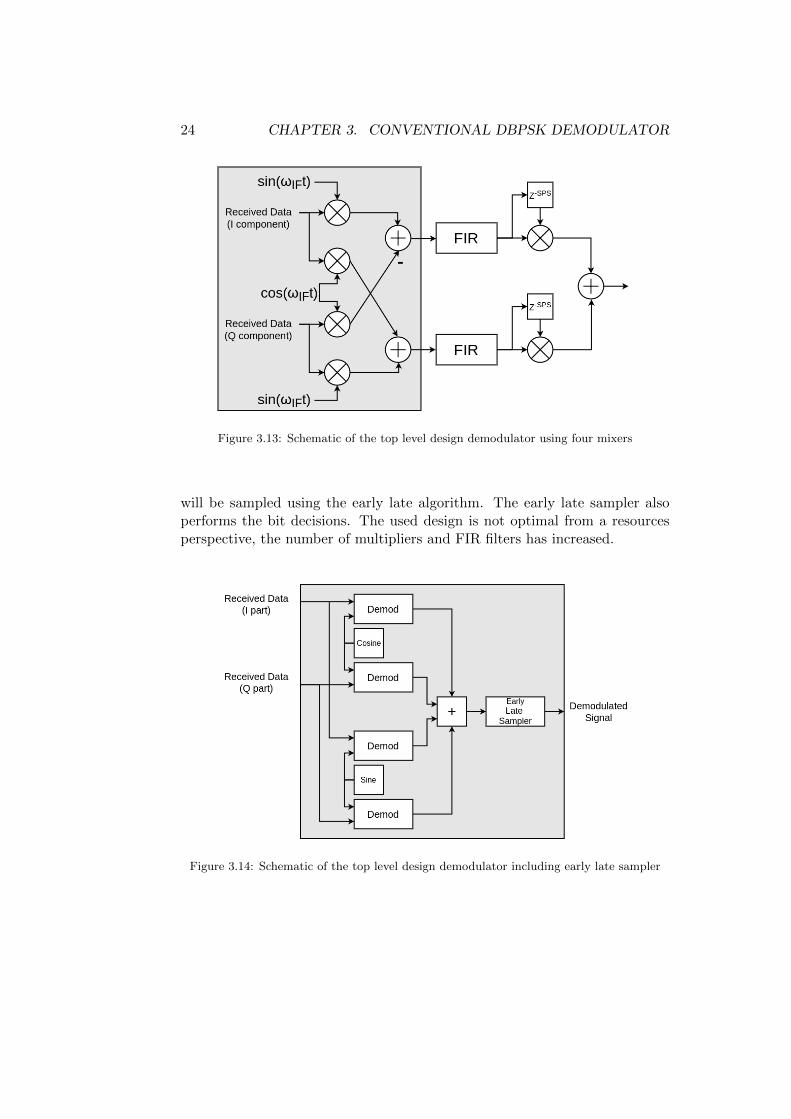
24 CHAPTER 3. CONVENTIONAL DBPSK DEMODULATOR
Figure 3.13: Schematic of the top level design demodulator using four mixers
will be sampled using the early late algorithm. The early late sampler alsoperforms the bit decisions. The used design is not optimal from a resourcesperspective, the number of multipliers and FIR filters has increased.
Figure 3.14: Schematic of the top level design demodulator including early late sampler
3.2. IMPLEMENTATION 25
3.2 Implementation
3.2.1 GNURadio
The test set-up, of which the description will follow in Section 3.3, makesuse of software called GNURadio. With this software it is possible to designsoftware defined radios. In GNURadio it is possible to create signal processingflow graphs. The flow graphs can be created with blocks that are included inthe software. Besides the standard blocks, the software offers the possibilityto define custom blocks. These blocks can be written in C++ or Python.
At the CAES group there are USRP (N210) boxes from Ettus Researchavailable. With these boxes it is possible to output an analogue RF signalthat was defined in GNURadio. The boxes can also receive signals from theirinput.
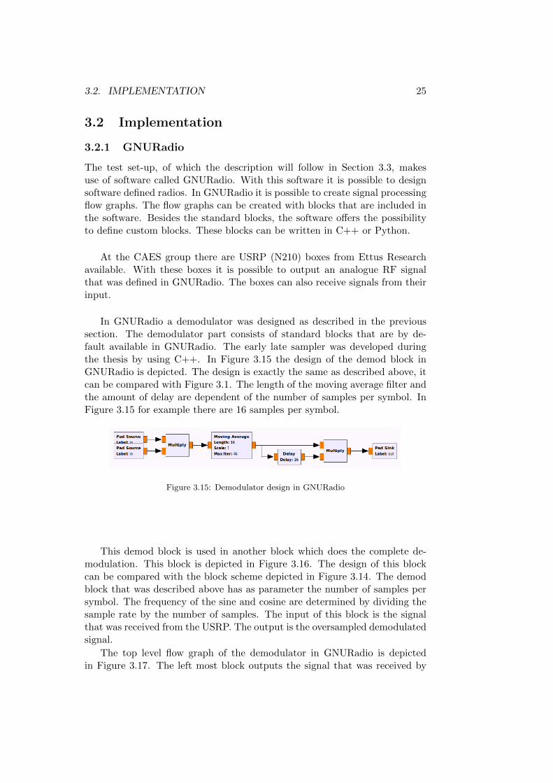
In GNURadio a demodulator was designed as described in the previoussection. The demodulator part consists of standard blocks that are by de-fault available in GNURadio. The early late sampler was developed duringthe thesis by using C++. In Figure 3.15 the design of the demod block inGNURadio is depicted. The design is exactly the same as described above, itcan be compared with Figure 3.1. The length of the moving average filter andthe amount of delay are dependent of the number of samples per symbol. InFigure 3.15 for example there are 16 samples per symbol.
Figure 3.15: Demodulator design in GNURadio
This demod block is used in another block which does the complete de-modulation. This block is depicted in Figure 3.16. The design of this blockcan be compared with the block scheme depicted in Figure 3.14. The demodblock that was described above has as parameter the number of samples persymbol. The frequency of the sine and cosine are determined by dividing thesample rate by the number of samples. The input of this block is the signalthat was received from the USRP. The output is the oversampled demodulatedsignal.
The top level flow graph of the demodulator in GNURadio is depictedin Figure 3.17. The left most block outputs the signal that was received by
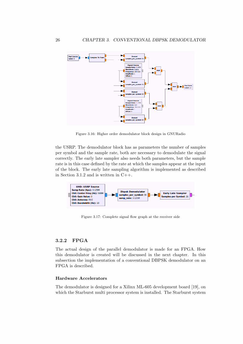
26 CHAPTER 3. CONVENTIONAL DBPSK DEMODULATOR
Figure 3.16: Higher order demodulator block design in GNURadio
the USRP. The demodulator block has as parameters the number of samplesper symbol and the sample rate, both are necessary to demodulate the signalcorrectly. The early late sampler also needs both parameters, but the samplerate is in this case defined by the rate at which the samples appear at the inputof the block. The early late sampling algorithm is implemented as describedin Section 3.1.2 and is written in C++.
Figure 3.17: Complete signal flow graph at the receiver side
3.2.2 FPGA
The actual design of the parallel demodulator is made for an FPGA. Howthis demodulator is created will be discussed in the next chapter. In thissubsection the implementation of a conventional DBPSK demodulator on anFPGA is described.
Hardware Accelerators
The demodulator is designed for a Xilinx ML-605 development board [19], onwhich the Starburst multi processor system is installed. The Starburst system
3.2. IMPLEMENTATION 27
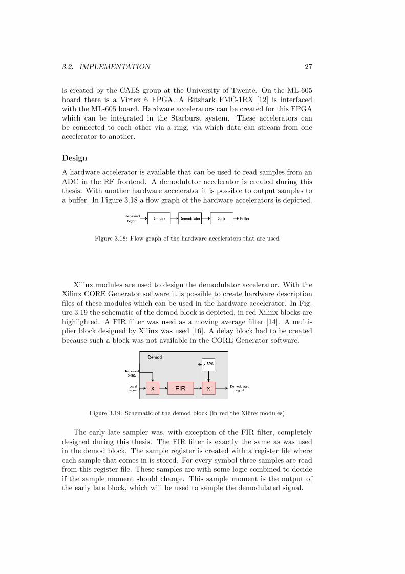
is created by the CAES group at the University of Twente. On the ML-605board there is a Virtex 6 FPGA. A Bitshark FMC-1RX [12] is interfacedwith the ML-605 board. Hardware accelerators can be created for this FPGAwhich can be integrated in the Starburst system. These accelerators canbe connected to each other via a ring, via which data can stream from oneaccelerator to another.
Design
A hardware accelerator is available that can be used to read samples from anADC in the RF frontend. A demodulator accelerator is created during thisthesis. With another hardware accelerator it is possible to output samples toa buffer. In Figure 3.18 a flow graph of the hardware accelerators is depicted.
Figure 3.18: Flow graph of the hardware accelerators that are used
Xilinx modules are used to design the demodulator accelerator. With theXilinx CORE Generator software it is possible to create hardware descriptionfiles of these modules which can be used in the hardware accelerator. In Fig-ure 3.19 the schematic of the demod block is depicted, in red Xilinx blocks arehighlighted. A FIR filter was used as a moving average filter [14]. A multi-plier block designed by Xilinx was used [16]. A delay block had to be createdbecause such a block was not available in the CORE Generator software.
Figure 3.19: Schematic of the demod block (in red the Xilinx modules)
The early late sampler was, with exception of the FIR filter, completelydesigned during this thesis. The FIR filter is exactly the same as was usedin the demod block. The sample register is created with a register file whereeach sample that comes in is stored. For every symbol three samples are readfrom this register file. These samples are with some logic combined to decideif the sample moment should change. This sample moment is the output ofthe early late block, which will be used to sample the demodulated signal.
28 CHAPTER 3. CONVENTIONAL DBPSK DEMODULATOR
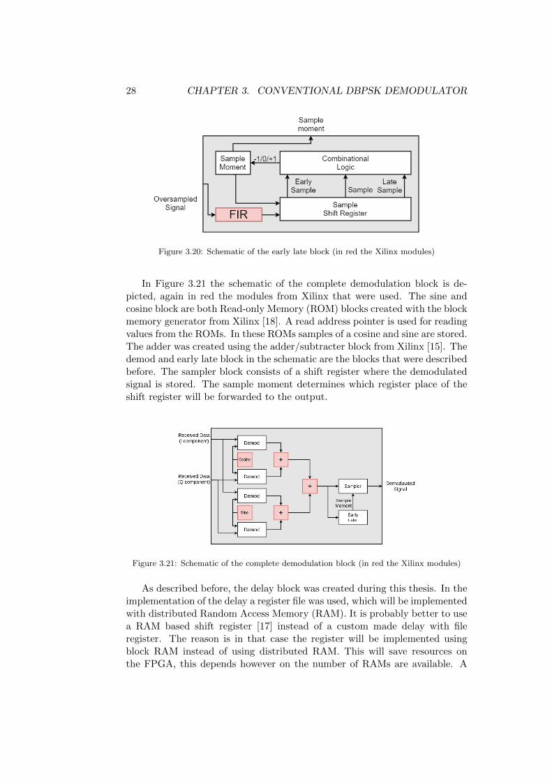
Figure 3.20: Schematic of the early late block (in red the Xilinx modules)
In Figure 3.21 the schematic of the complete demodulation block is de-picted, again in red the modules from Xilinx that were used. The sine andcosine block are both Read-only Memory (ROM) blocks created with the blockmemory generator from Xilinx [18]. A read address pointer is used for readingvalues from the ROMs. In these ROMs samples of a cosine and sine are stored.The adder was created using the adder/subtracter block from Xilinx [15]. Thedemod and early late block in the schematic are the blocks that were describedbefore. The sampler block consists of a shift register where the demodulatedsignal is stored. The sample moment determines which register place of theshift register will be forwarded to the output.
Figure 3.21: Schematic of the complete demodulation block (in red the Xilinx modules)
As described before, the delay block was created during this thesis. In theimplementation of the delay a register file was used, which will be implementedwith distributed Random Access Memory (RAM). It is probably better to usea RAM based shift register [17] instead of a custom made delay with fileregister. The reason is in that case the register will be implemented usingblock RAM instead of using distributed RAM. This will save resources onthe FPGA, this depends however on the number of RAMs are available. A
3.3. RESULTS 29
implementation test shows that when a RAM based shift register is used thisis optimised without using RAM blocks. However when the standard Xilinxblock is used the chance of bugs in the design is smaller. The same blockcan also be used for the sampler block, in that case the option for variablelength should be used to be able to use the right sample moment. When thesemodifications are applied to the design only the early late block contains selfdefined blocks. By using the blocks that are created by Xilinx the createdhardware will probably be more efficient.
3.3 Results
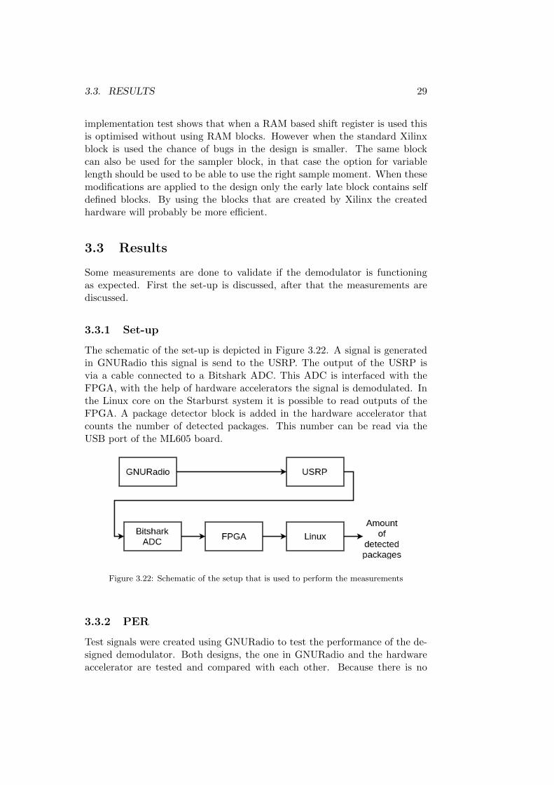
Some measurements are done to validate if the demodulator is functioningas expected. First the set-up is discussed, after that the measurements arediscussed.
3.3.1 Set-up
The schematic of the set-up is depicted in Figure 3.22. A signal is generatedin GNURadio this signal is send to the USRP. The output of the USRP isvia a cable connected to a Bitshark ADC. This ADC is interfaced with theFPGA, with the help of hardware accelerators the signal is demodulated. Inthe Linux core on the Starburst system it is possible to read outputs of theFPGA. A package detector block is added in the hardware accelerator thatcounts the number of detected packages. This number can be read via theUSB port of the ML605 board.
Figure 3.22: Schematic of the setup that is used to perform the measurements
3.3.2 PER
Test signals were created using GNURadio to test the performance of the de-signed demodulator. Both designs, the one in GNURadio and the hardwareaccelerator are tested and compared with each other. Because there is no
30 CHAPTER 3. CONVENTIONAL DBPSK DEMODULATOR
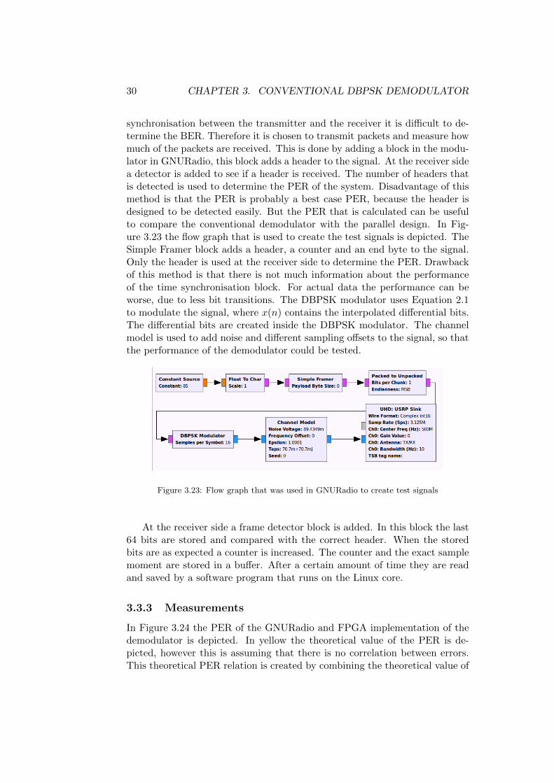
synchronisation between the transmitter and the receiver it is difficult to de-termine the BER. Therefore it is chosen to transmit packets and measure howmuch of the packets are received. This is done by adding a block in the modu-lator in GNURadio, this block adds a header to the signal. At the receiver sidea detector is added to see if a header is received. The number of headers thatis detected is used to determine the PER of the system. Disadvantage of thismethod is that the PER is probably a best case PER, because the header isdesigned to be detected easily. But the PER that is calculated can be usefulto compare the conventional demodulator with the parallel design. In Fig-ure 3.23 the flow graph that is used to create the test signals is depicted. TheSimple Framer block adds a header, a counter and an end byte to the signal.Only the header is used at the receiver side to determine the PER. Drawbackof this method is that there is not much information about the performanceof the time synchronisation block. For actual data the performance can beworse, due to less bit transitions. The DBPSK modulator uses Equation 2.1to modulate the signal, where x(n) contains the interpolated differential bits.The differential bits are created inside the DBPSK modulator. The channelmodel is used to add noise and different sampling offsets to the signal, so thatthe performance of the demodulator could be tested.
Figure 3.23: Flow graph that was used in GNURadio to create test signals
At the receiver side a frame detector block is added. In this block the last64 bits are stored and compared with the correct header. When the storedbits are as expected a counter is increased. The counter and the exact samplemoment are stored in a buffer. After a certain amount of time they are readand saved by a software program that runs on the Linux core.
3.3.3 Measurements
In Figure 3.24 the PER of the GNURadio and FPGA implementation of thedemodulator is depicted. In yellow the theoretical value of the PER is de-picted, however this is assuming that there is no correlation between errors.This theoretical PER relation is created by combining the theoretical value of
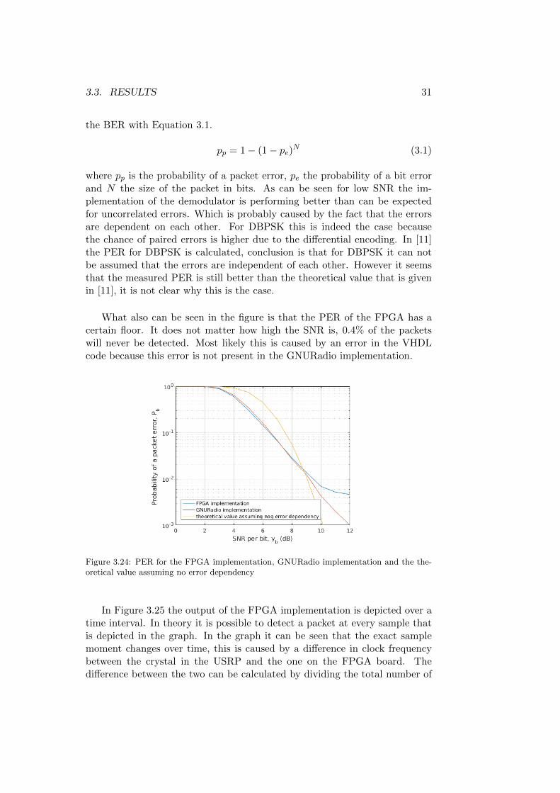
3.3. RESULTS 31
the BER with Equation 3.1.
pp = 1− (1− pe)N (3.1)
where pp is the probability of a packet error, pe the probability of a bit errorand N the size of the packet in bits. As can be seen for low SNR the im-plementation of the demodulator is performing better than can be expectedfor uncorrelated errors. Which is probably caused by the fact that the errorsare dependent on each other. For DBPSK this is indeed the case becausethe chance of paired errors is higher due to the differential encoding. In [11]the PER for DBPSK is calculated, conclusion is that for DBPSK it can notbe assumed that the errors are independent of each other. However it seemsthat the measured PER is still better than the theoretical value that is givenin [11], it is not clear why this is the case.
What also can be seen in the figure is that the PER of the FPGA has acertain floor. It does not matter how high the SNR is, 0.4% of the packetswill never be detected. Most likely this is caused by an error in the VHDLcode because this error is not present in the GNURadio implementation.
Figure 3.24: PER for the FPGA implementation, GNURadio implementation and the the-oretical value assuming no error dependency
In Figure 3.25 the output of the FPGA implementation is depicted over atime interval. In theory it is possible to detect a packet at every sample thatis depicted in the graph. In the graph it can be seen that the exact samplemoment changes over time, this is caused by a difference in clock frequencybetween the crystal in the USRP and the one on the FPGA board. Thedifference between the two can be calculated by dividing the total number of
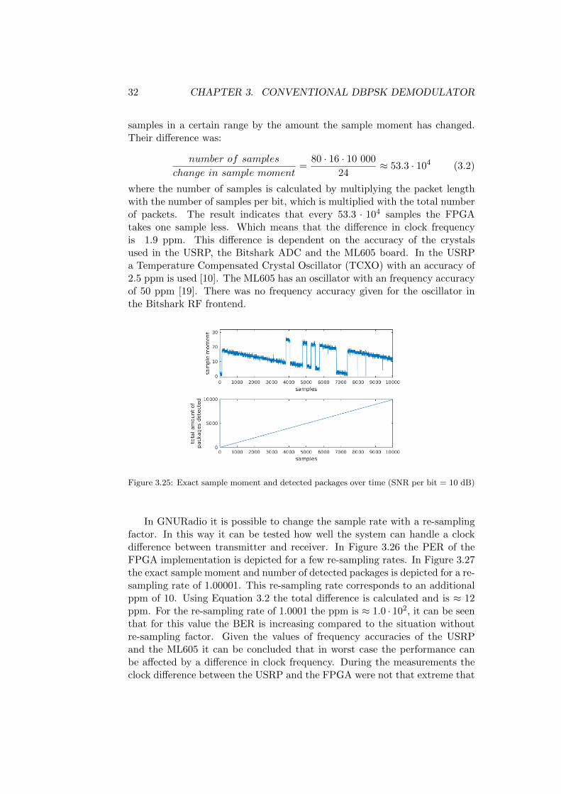
32 CHAPTER 3. CONVENTIONAL DBPSK DEMODULATOR
samples in a certain range by the amount the sample moment has changed.Their difference was:
number of samples
change in sample moment=
80 · 16 · 10 000
24≈ 53.3 · 104 (3.2)
where the number of samples is calculated by multiplying the packet lengthwith the number of samples per bit, which is multiplied with the total numberof packets. The result indicates that every 53.3 · 104 samples the FPGAtakes one sample less. Which means that the difference in clock frequencyis 1.9 ppm. This difference is dependent on the accuracy of the crystalsused in the USRP, the Bitshark ADC and the ML605 board. In the USRPa Temperature Compensated Crystal Oscillator (TCXO) with an accuracy of2.5 ppm is used [10]. The ML605 has an oscillator with an frequency accuracyof 50 ppm [19]. There was no frequency accuracy given for the oscillator inthe Bitshark RF frontend.
Figure 3.25: Exact sample moment and detected packages over time (SNR per bit = 10 dB)
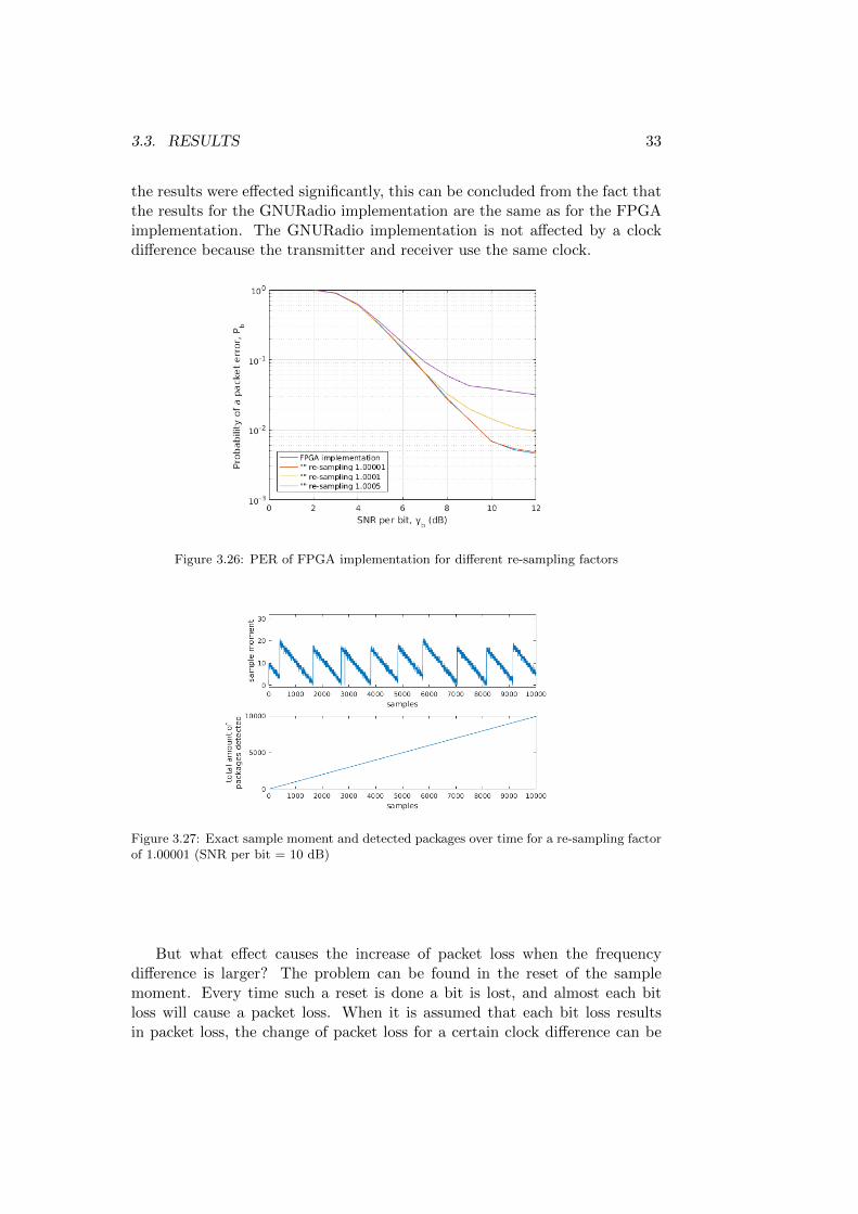
In GNURadio it is possible to change the sample rate with a re-samplingfactor. In this way it can be tested how well the system can handle a clockdifference between transmitter and receiver. In Figure 3.26 the PER of theFPGA implementation is depicted for a few re-sampling rates. In Figure 3.27the exact sample moment and number of detected packages is depicted for a re-sampling rate of 1.00001. This re-sampling rate corresponds to an additionalppm of 10. Using Equation 3.2 the total difference is calculated and is ≈ 12ppm. For the re-sampling rate of 1.0001 the ppm is ≈ 1.0 · 102, it can be seenthat for this value the BER is increasing compared to the situation withoutre-sampling factor. Given the values of frequency accuracies of the USRPand the ML605 it can be concluded that in worst case the performance canbe affected by a difference in clock frequency. During the measurements theclock difference between the USRP and the FPGA were not that extreme that
3.3. RESULTS 33
the results were effected significantly, this can be concluded from the fact thatthe results for the GNURadio implementation are the same as for the FPGAimplementation. The GNURadio implementation is not affected by a clockdifference because the transmitter and receiver use the same clock.
Figure 3.26: PER of FPGA implementation for different re-sampling factors
Figure 3.27: Exact sample moment and detected packages over time for a re-sampling factorof 1.00001 (SNR per bit = 10 dB)
But what effect causes the increase of packet loss when the frequencydifference is larger? The problem can be found in the reset of the samplemoment. Every time such a reset is done a bit is lost, and almost each bitloss will cause a packet loss. When it is assumed that each bit loss resultsin packet loss, the change of packet loss for a certain clock difference can be
34 CHAPTER 3. CONVENTIONAL DBPSK DEMODULATOR
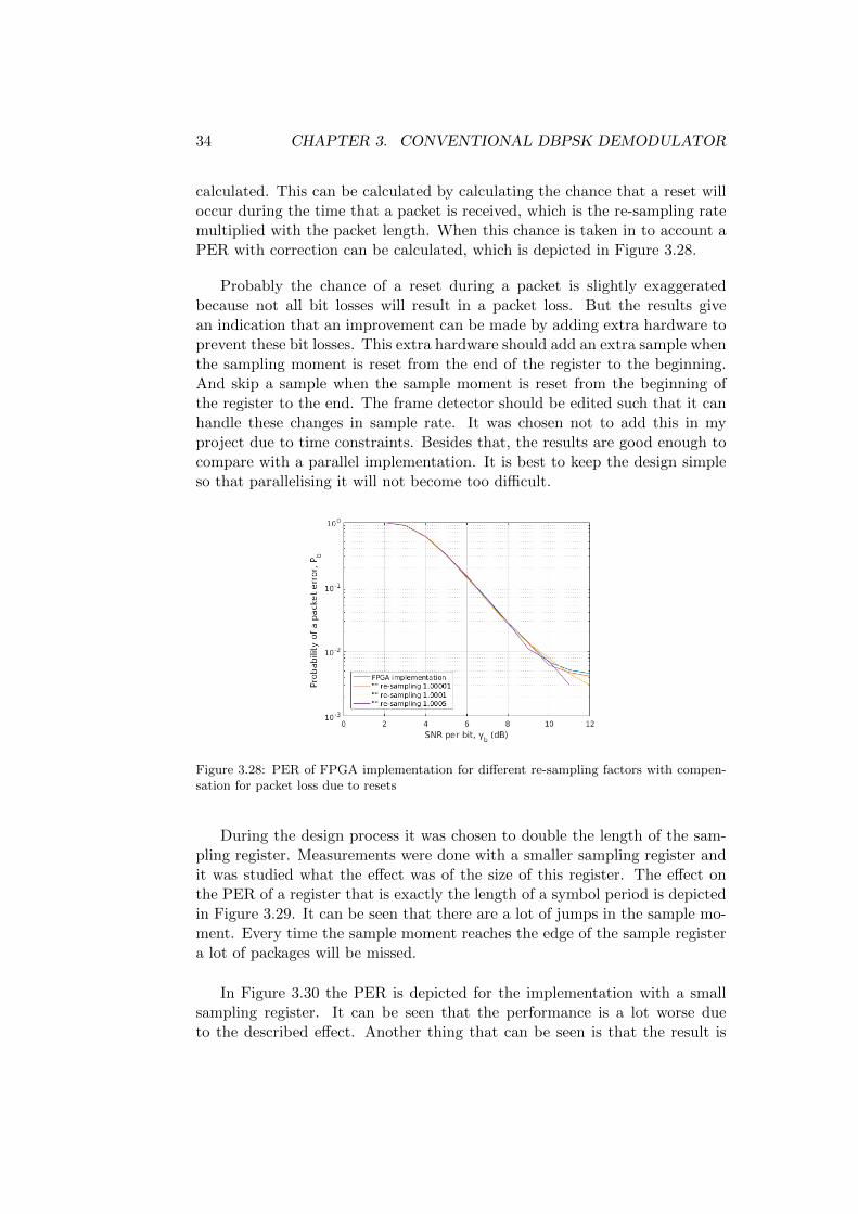
calculated. This can be calculated by calculating the chance that a reset willoccur during the time that a packet is received, which is the re-sampling ratemultiplied with the packet length. When this chance is taken in to account aPER with correction can be calculated, which is depicted in Figure 3.28.
Probably the chance of a reset during a packet is slightly exaggeratedbecause not all bit losses will result in a packet loss. But the results givean indication that an improvement can be made by adding extra hardware toprevent these bit losses. This extra hardware should add an extra sample whenthe sampling moment is reset from the end of the register to the beginning.And skip a sample when the sample moment is reset from the beginning ofthe register to the end. The frame detector should be edited such that it canhandle these changes in sample rate. It was chosen not to add this in myproject due to time constraints. Besides that, the results are good enough tocompare with a parallel implementation. It is best to keep the design simpleso that parallelising it will not become too difficult.
Figure 3.28: PER of FPGA implementation for different re-sampling factors with compen-sation for packet loss due to resets
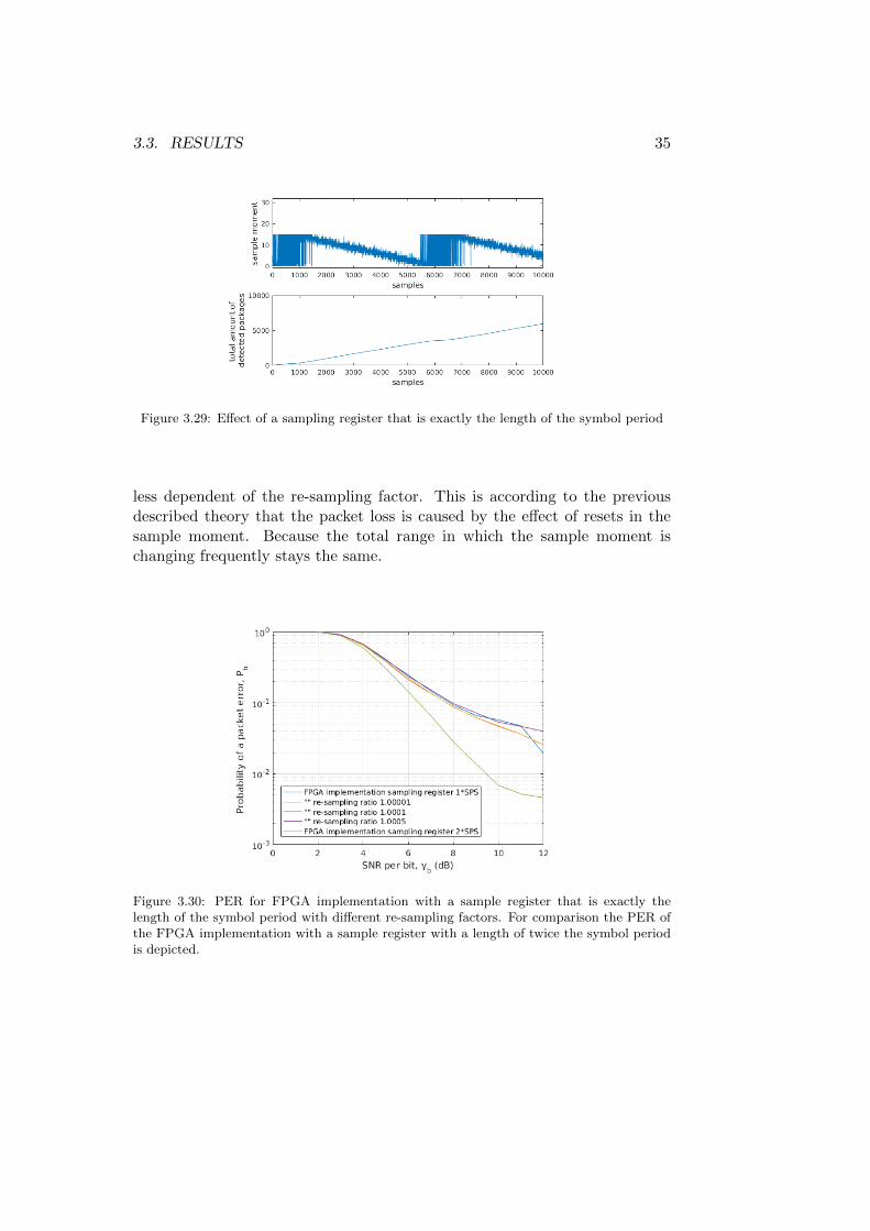
During the design process it was chosen to double the length of the sam-pling register. Measurements were done with a smaller sampling register andit was studied what the effect was of the size of this register. The effect onthe PER of a register that is exactly the length of a symbol period is depictedin Figure 3.29. It can be seen that there are a lot of jumps in the sample mo-ment. Every time the sample moment reaches the edge of the sample registera lot of packages will be missed.
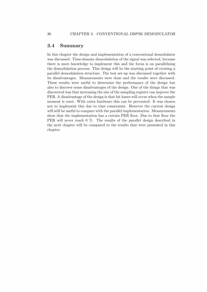
In Figure 3.30 the PER is depicted for the implementation with a smallsampling register. It can be seen that the performance is a lot worse dueto the described effect. Another thing that can be seen is that the result is
3.3. RESULTS 35
Figure 3.29: Effect of a sampling register that is exactly the length of the symbol period
less dependent of the re-sampling factor. This is according to the previousdescribed theory that the packet loss is caused by the effect of resets in thesample moment. Because the total range in which the sample moment ischanging frequently stays the same.
Figure 3.30: PER for FPGA implementation with a sample register that is exactly thelength of the symbol period with different re-sampling factors. For comparison the PER ofthe FPGA implementation with a sample register with a length of twice the symbol periodis depicted.
36 CHAPTER 3. CONVENTIONAL DBPSK DEMODULATOR
3.4 Summary
In this chapter the design and implementation of a conventional demodulatorwas discussed. Time-domain demodulation of the signal was selected, becausethere is more knowledge to implement this and the focus is on parallelisingthe demodulation process. This design will be the starting point of creating aparallel demodulation structure. The test set-up was discussed together withits disadvantages. Measurements were done and the results were discussed.These results were useful to determine the performance of the design butalso to discover some disadvantages of the design. One of the things that wasdiscovered was that increasing the size of the sampling register can improve thePER. A disadvantage of the design is that bit losses will occur when the samplemoment is reset. With extra hardware this can be prevented. It was chosennot to implement this due to time constraints. However the current designwill still be useful to compare with the parallel implementation. Measurementsshow that the implementation has a certain PER floor. Due to that floor thePER will never reach 0 %. The results of the parallel design described inthe next chapter will be compared to the results that were presented in thischapter.
CHAPTER 4Parallel DBPSK Demodulator
37
38 CHAPTER 4. PARALLEL DBPSK DEMODULATOR
Subject of this thesis is to design a demodulator on an FPGA which canhandle high data rates. To do so a parallel demodulator is designed. In thischapter the design of such a demodulator is discussed. In the previous chapterthe design of a conventional DBPSK demodulator was discussed, this designwill be the basis of the parallel design. This parallel design will be discussedin this chapter. After which the discussion of the implementation follows.The implementation that is discussed in this chapter will be used in the nextchapter to test the performance and compare it with the conventional design.
4.1 Design
An FMC125 ADC of 4DSP [1] was available at the CAES group which hasa possibility to sample at 5Gs/s. At this high speed it delivers its samplesusing 8 parallel channels. However it is from time perspective decided not touse this because it is not interfaced with the Starburst platform yet. Insteada proof of concept is made which can be used to work with parallel samples.It is chosen to create a switch module that switches packets of samples todifferent demodulation modules. In the next section the functioning of thisswitch is discussed.
4.1.1 Switch
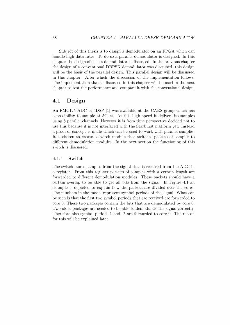
The switch stores samples from the signal that is received from the ADC ina register. From this register packets of samples with a certain length areforwarded to different demodulation modules. These packets should have acertain overlap to be able to get all bits from the signal. In Figure 4.1 anexample is depicted to explain how the packets are divided over the cores.The numbers in the model represent symbol periods of the signal. What canbe seen is that the first two symbol periods that are received are forwarded tocore 0. These two packages contain the bits that are demodulated by core 0.Two older packages are needed to be able to demodulate the signal correctly.Therefore also symbol period -1 and -2 are forwarded to core 0. The reasonfor this will be explained later.
4.1. DESIGN 39
Figure 4.1: Illustration of the functioning of the switch
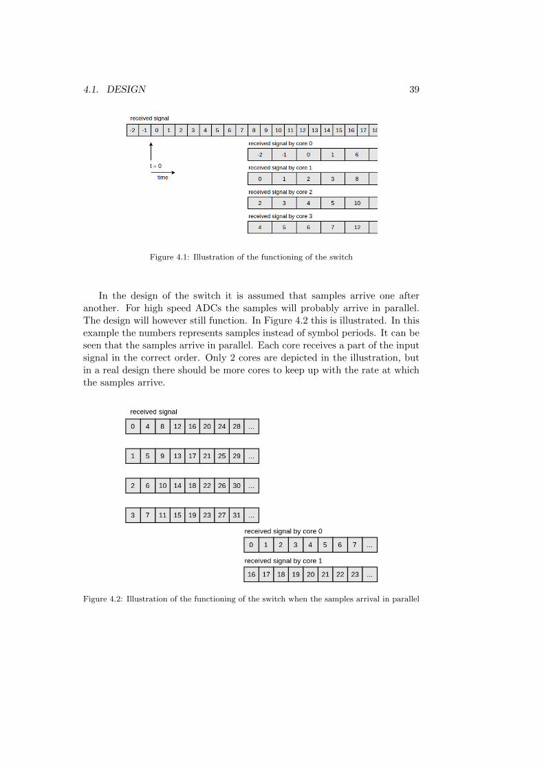
In the design of the switch it is assumed that samples arrive one afteranother. For high speed ADCs the samples will probably arrive in parallel.The design will however still function. In Figure 4.2 this is illustrated. In thisexample the numbers represents samples instead of symbol periods. It can beseen that the samples arrive in parallel. Each core receives a part of the inputsignal in the correct order. Only 2 cores are depicted in the illustration, butin a real design there should be more cores to keep up with the rate at whichthe samples arrive.
Figure 4.2: Illustration of the functioning of the switch when the samples arrival in parallel
40 CHAPTER 4. PARALLEL DBPSK DEMODULATOR
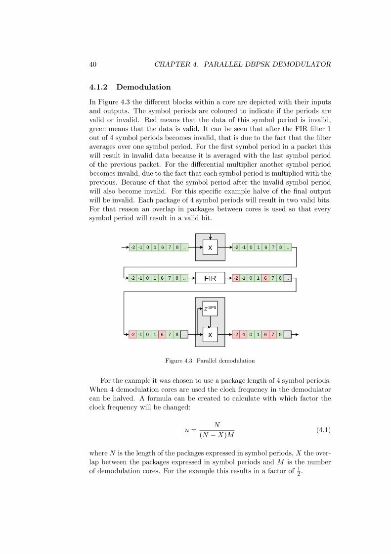
4.1.2 Demodulation
In Figure 4.3 the different blocks within a core are depicted with their inputsand outputs. The symbol periods are coloured to indicate if the periods arevalid or invalid. Red means that the data of this symbol period is invalid,green means that the data is valid. It can be seen that after the FIR filter 1out of 4 symbol periods becomes invalid, that is due to the fact that the filteraverages over one symbol period. For the first symbol period in a packet thiswill result in invalid data because it is averaged with the last symbol periodof the previous packet. For the differential multiplier another symbol periodbecomes invalid, due to the fact that each symbol period is multiplied with theprevious. Because of that the symbol period after the invalid symbol periodwill also become invalid. For this specific example halve of the final outputwill be invalid. Each package of 4 symbol periods will result in two valid bits.For that reason an overlap in packages between cores is used so that everysymbol period will result in a valid bit.
Figure 4.3: Parallel demodulation
For the example it was chosen to use a package length of 4 symbol periods.When 4 demodulation cores are used the clock frequency in the demodulatorcan be halved. A formula can be created to calculate with which factor theclock frequency will be changed:
n =N
(N −X)M(4.1)
where N is the length of the packages expressed in symbol periods, X the over-lap between the packages expressed in symbol periods and M is the numberof demodulation cores. For the example this results in a factor of 1
2 .
4.1. DESIGN 41
In the previous chapter it was discussed how long the sampling registershould be. When a sampling register is used that has a length of twice thesymbol period the overlap between packets should increase to 3 symbol periodsinstead of 2. In that case the previous example will not result in a decrease ofthe clock frequency. The length of the packages or the number of cores shouldbe increased to still have a lower clock frequency in the demodulator. Forexample 8 demodulation cores could be used instead to still be able to halvethe clock frequency. In that case each core would extract one bit out of eachpackage.
4.1.3 Symbol Time Recovery
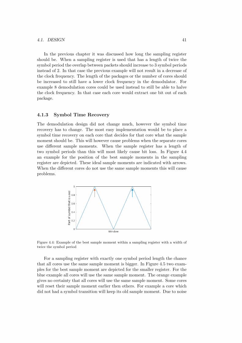
The demodulation design did not change much, however the symbol timerecovery has to change. The most easy implementation would be to place asymbol time recovery on each core that decides for that core what the samplemoment should be. This will however cause problems when the separate coresuse different sample moments. When the sample register has a length oftwo symbol periods than this will most likely cause bit loss. In Figure 4.4an example for the position of the best sample moments in the samplingregister are depicted. These ideal sample moments are indicated with arrows.When the different cores do not use the same sample moments this will causeproblems.
Figure 4.4: Example of the best sample moment within a sampling register with a width oftwice the symbol period
For a sampling register with exactly one symbol period length the chancethat all cores use the same sample moment is bigger. In Figure 4.5 two exam-ples for the best sample moment are depicted for the smaller register. For theblue example all cores will use the same sample moment. The orange examplegives no certainty that all cores will use the same sample moment. Some coreswill reset their sample moment earlier then others. For example a core whichdid not had a symbol transition will keep its old sample moment. Due to noise
42 CHAPTER 4. PARALLEL DBPSK DEMODULATOR
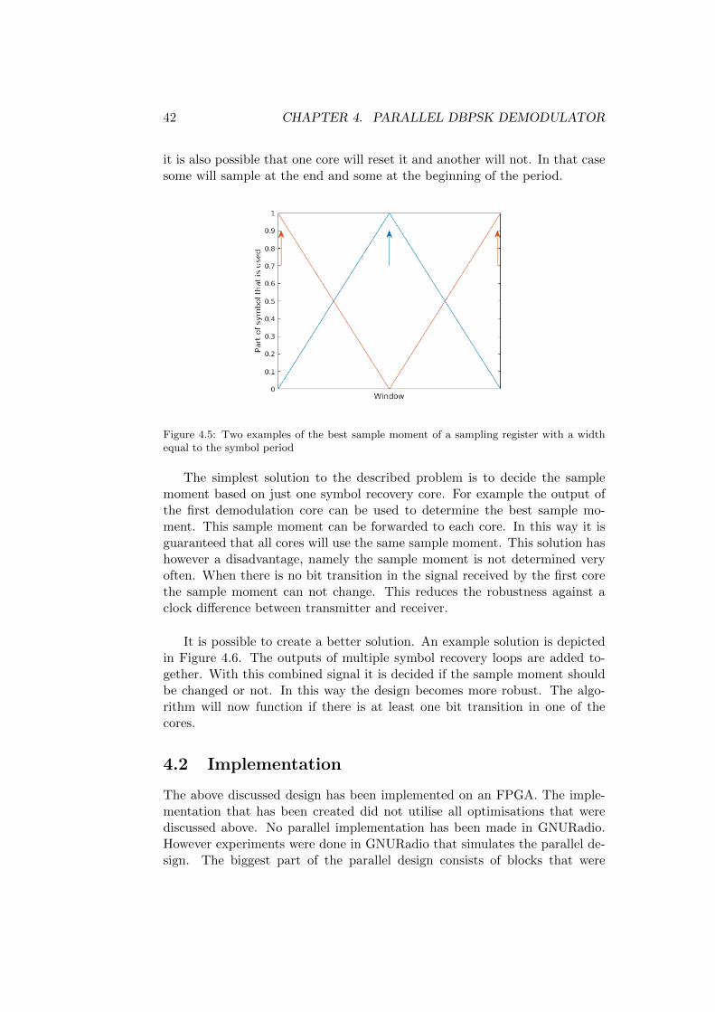
it is also possible that one core will reset it and another will not. In that casesome will sample at the end and some at the beginning of the period.
Figure 4.5: Two examples of the best sample moment of a sampling register with a widthequal to the symbol period
The simplest solution to the described problem is to decide the samplemoment based on just one symbol recovery core. For example the output ofthe first demodulation core can be used to determine the best sample mo-ment. This sample moment can be forwarded to each core. In this way it isguaranteed that all cores will use the same sample moment. This solution hashowever a disadvantage, namely the sample moment is not determined veryoften. When there is no bit transition in the signal received by the first corethe sample moment can not change. This reduces the robustness against aclock difference between transmitter and receiver.
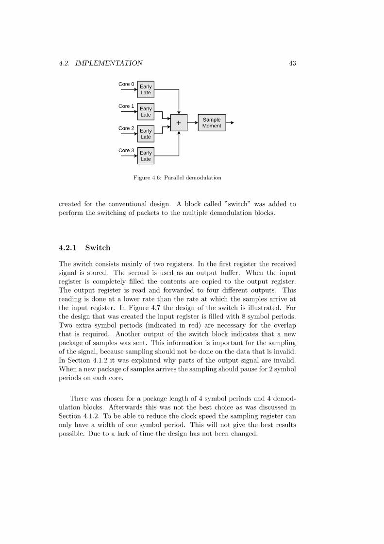
It is possible to create a better solution. An example solution is depictedin Figure 4.6. The outputs of multiple symbol recovery loops are added to-gether. With this combined signal it is decided if the sample moment shouldbe changed or not. In this way the design becomes more robust. The algo-rithm will now function if there is at least one bit transition in one of thecores.
4.2 Implementation
The above discussed design has been implemented on an FPGA. The imple-mentation that has been created did not utilise all optimisations that werediscussed above. No parallel implementation has been made in GNURadio.However experiments were done in GNURadio that simulates the parallel de-sign. The biggest part of the parallel design consists of blocks that were
4.2. IMPLEMENTATION 43
Figure 4.6: Parallel demodulation
created for the conventional design. A block called ”switch” was added toperform the switching of packets to the multiple demodulation blocks.
4.2.1 Switch
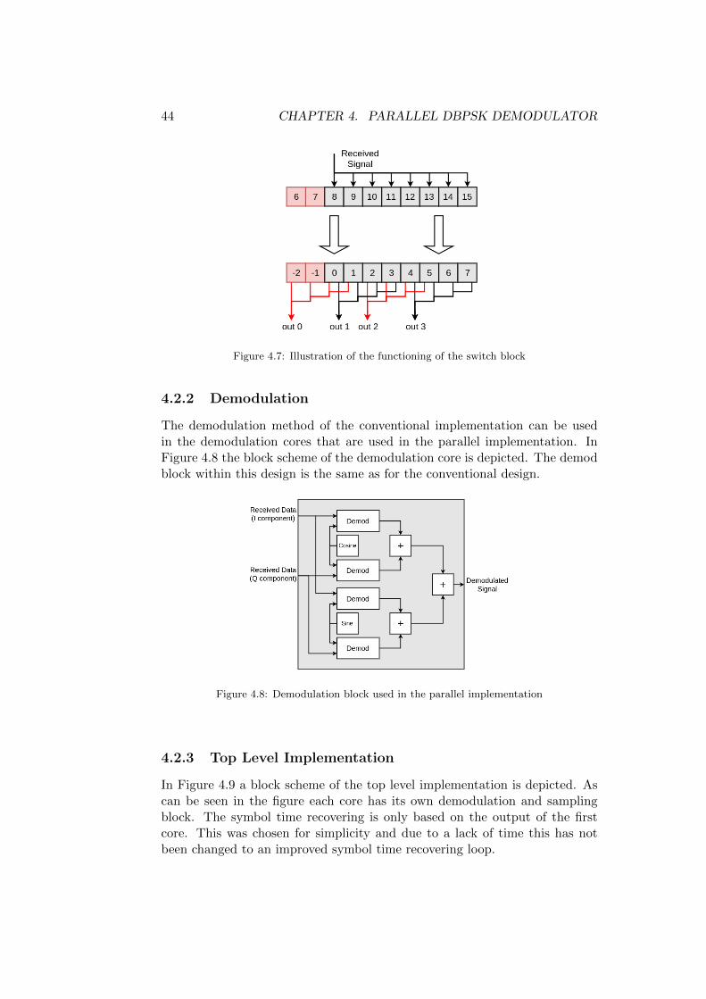
The switch consists mainly of two registers. In the first register the receivedsignal is stored. The second is used as an output buffer. When the inputregister is completely filled the contents are copied to the output register.The output register is read and forwarded to four different outputs. Thisreading is done at a lower rate than the rate at which the samples arrive atthe input register. In Figure 4.7 the design of the switch is illustrated. Forthe design that was created the input register is filled with 8 symbol periods.Two extra symbol periods (indicated in red) are necessary for the overlapthat is required. Another output of the switch block indicates that a newpackage of samples was sent. This information is important for the samplingof the signal, because sampling should not be done on the data that is invalid.In Section 4.1.2 it was explained why parts of the output signal are invalid.When a new package of samples arrives the sampling should pause for 2 symbolperiods on each core.
There was chosen for a package length of 4 symbol periods and 4 demod-ulation blocks. Afterwards this was not the best choice as was discussed inSection 4.1.2. To be able to reduce the clock speed the sampling register canonly have a width of one symbol period. This will not give the best resultspossible. Due to a lack of time the design has not been changed.
44 CHAPTER 4. PARALLEL DBPSK DEMODULATOR
Figure 4.7: Illustration of the functioning of the switch block
4.2.2 Demodulation
The demodulation method of the conventional implementation can be usedin the demodulation cores that are used in the parallel implementation. InFigure 4.8 the block scheme of the demodulation core is depicted. The demodblock within this design is the same as for the conventional design.
Figure 4.8: Demodulation block used in the parallel implementation
4.2.3 Top Level Implementation
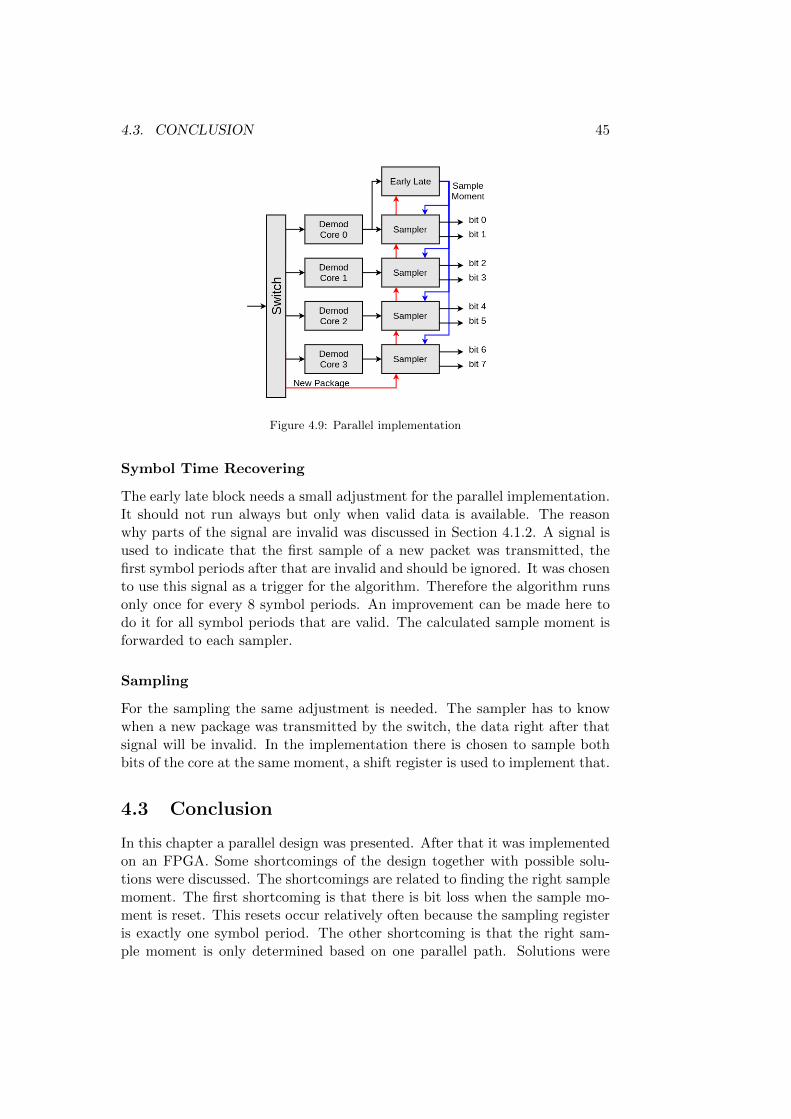
In Figure 4.9 a block scheme of the top level implementation is depicted. Ascan be seen in the figure each core has its own demodulation and samplingblock. The symbol time recovering is only based on the output of the firstcore. This was chosen for simplicity and due to a lack of time this has notbeen changed to an improved symbol time recovering loop.
4.3. CONCLUSION 45
Figure 4.9: Parallel implementation
Symbol Time Recovering
The early late block needs a small adjustment for the parallel implementation.It should not run always but only when valid data is available. The reasonwhy parts of the signal are invalid was discussed in Section 4.1.2. A signal isused to indicate that the first sample of a new packet was transmitted, thefirst symbol periods after that are invalid and should be ignored. It was chosento use this signal as a trigger for the algorithm. Therefore the algorithm runsonly once for every 8 symbol periods. An improvement can be made here todo it for all symbol periods that are valid. The calculated sample moment isforwarded to each sampler.
Sampling
For the sampling the same adjustment is needed. The sampler has to knowwhen a new package was transmitted by the switch, the data right after thatsignal will be invalid. In the implementation there is chosen to sample bothbits of the core at the same moment, a shift register is used to implement that.
4.3 Conclusion
In this chapter a parallel design was presented. After that it was implementedon an FPGA. Some shortcomings of the design together with possible solu-tions were discussed. The shortcomings are related to finding the right samplemoment. The first shortcoming is that there is bit loss when the sample mo-ment is reset. This resets occur relatively often because the sampling registeris exactly one symbol period. The other shortcoming is that the right sam-ple moment is only determined based on one parallel path. Solutions were
46 CHAPTER 4. PARALLEL DBPSK DEMODULATOR
presented that should overcome these shortcomings. However due to timeconstraint my design has still these shortcomings in it. In the next chaptermeasurement results of the presented parallel design are presented and the re-sults are compared with the results obtained using a conventional demodulatorthat has been presented in Chapter 3.
CHAPTER 5Results and Comparison
47
48 CHAPTER 5. RESULTS AND COMPARISON
In this chapter the results of the parallel demodulator are discussed. Theresults are compared with the results that were presented in Chapter 3. Theset-up that is used has already been explained in Section 3.3.1.
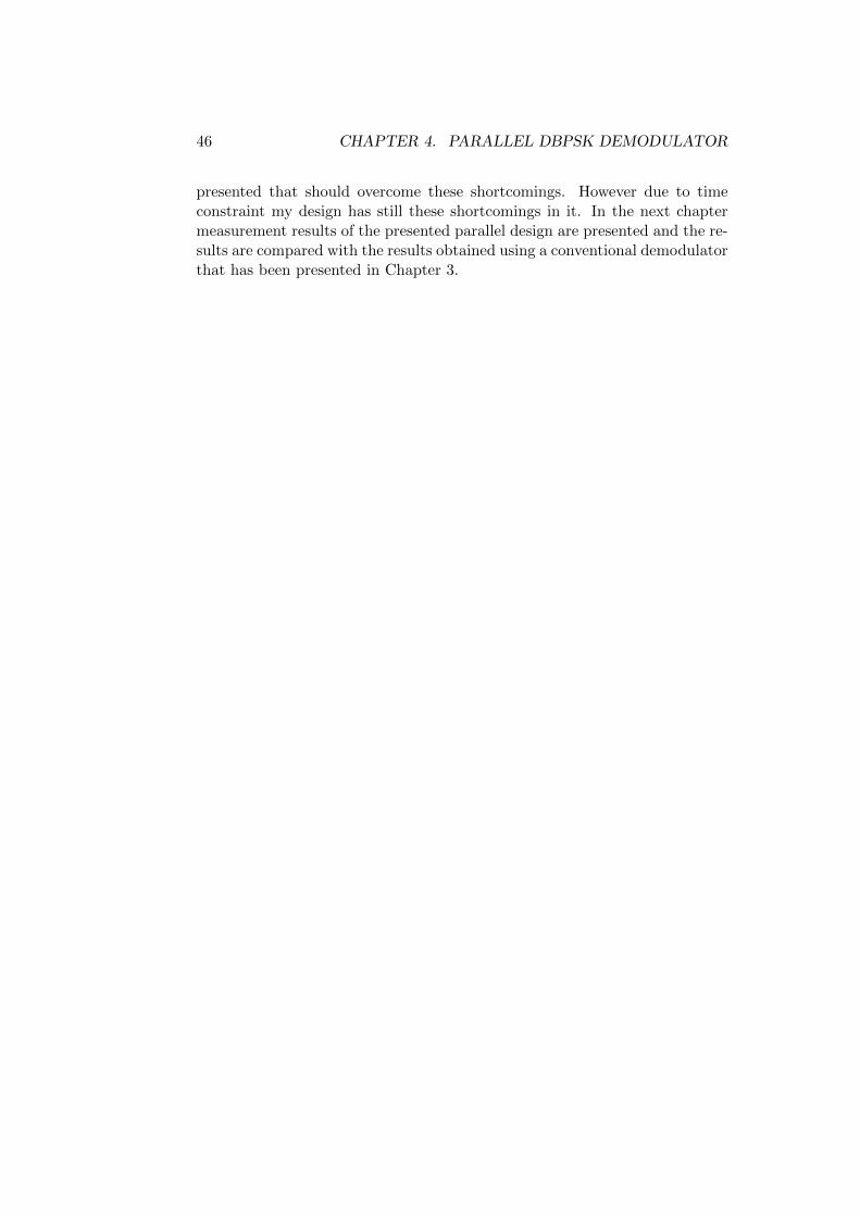
5.1 Results Parallel Receiver
In Figure 5.1 the PER of the parallel implementation on the FPGA is depictedfor several re-sampling rates. For comparison also the PER of the GNURadioimplementation is depicted. What can be seen is that the implementation isperforming worse than the GNURadio implementation. But this is probablydue to the fact that the sampling register has a width of only one symbol periodinstead of 2. Therefore it is useful to compare it with the other implementationon the FPGA that was made.
Figure 5.1: PER of parallel implementation for different re-sampling factors, for comparisonthe PER of the conventional implementation in GNURadio is also depicted.
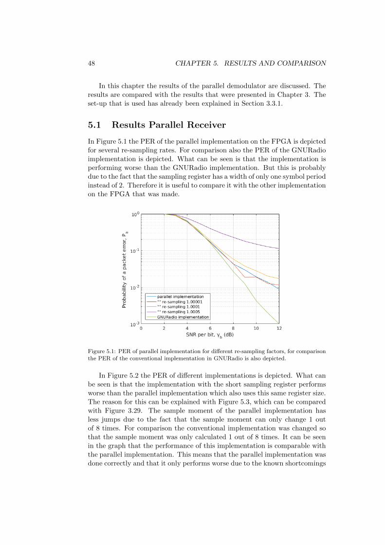
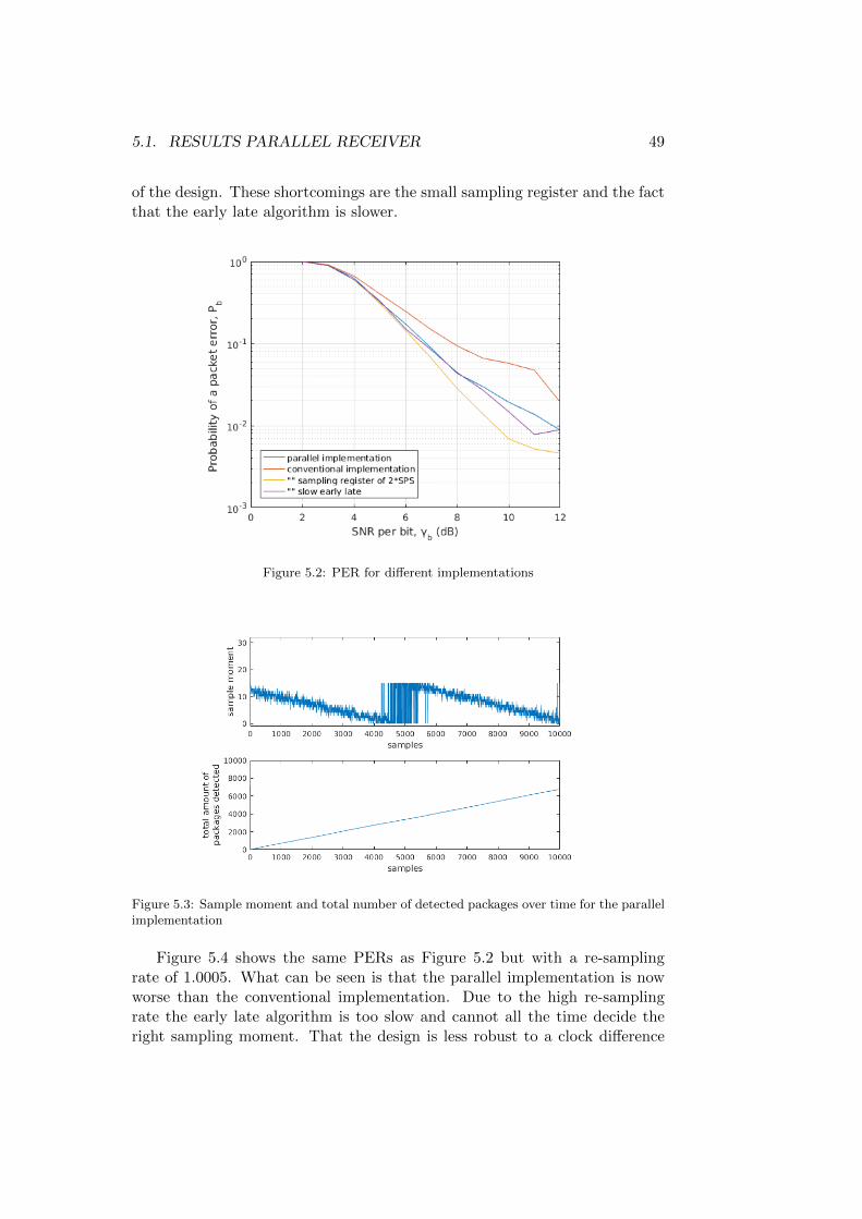
In Figure 5.2 the PER of different implementations is depicted. What canbe seen is that the implementation with the short sampling register performsworse than the parallel implementation which also uses this same register size.The reason for this can be explained with Figure 5.3, which can be comparedwith Figure 3.29. The sample moment of the parallel implementation hasless jumps due to the fact that the sample moment can only change 1 outof 8 times. For comparison the conventional implementation was changed sothat the sample moment was only calculated 1 out of 8 times. It can be seenin the graph that the performance of this implementation is comparable withthe parallel implementation. This means that the parallel implementation wasdone correctly and that it only performs worse due to the known shortcomings
5.1. RESULTS PARALLEL RECEIVER 49
of the design. These shortcomings are the small sampling register and the factthat the early late algorithm is slower.
Figure 5.2: PER for different implementations
Figure 5.3: Sample moment and total number of detected packages over time for the parallelimplementation
Figure 5.4 shows the same PERs as Figure 5.2 but with a re-samplingrate of 1.0005. What can be seen is that the parallel implementation is nowworse than the conventional implementation. Due to the high re-samplingrate the early late algorithm is too slow and cannot all the time decide theright sampling moment. That the design is less robust to a clock difference
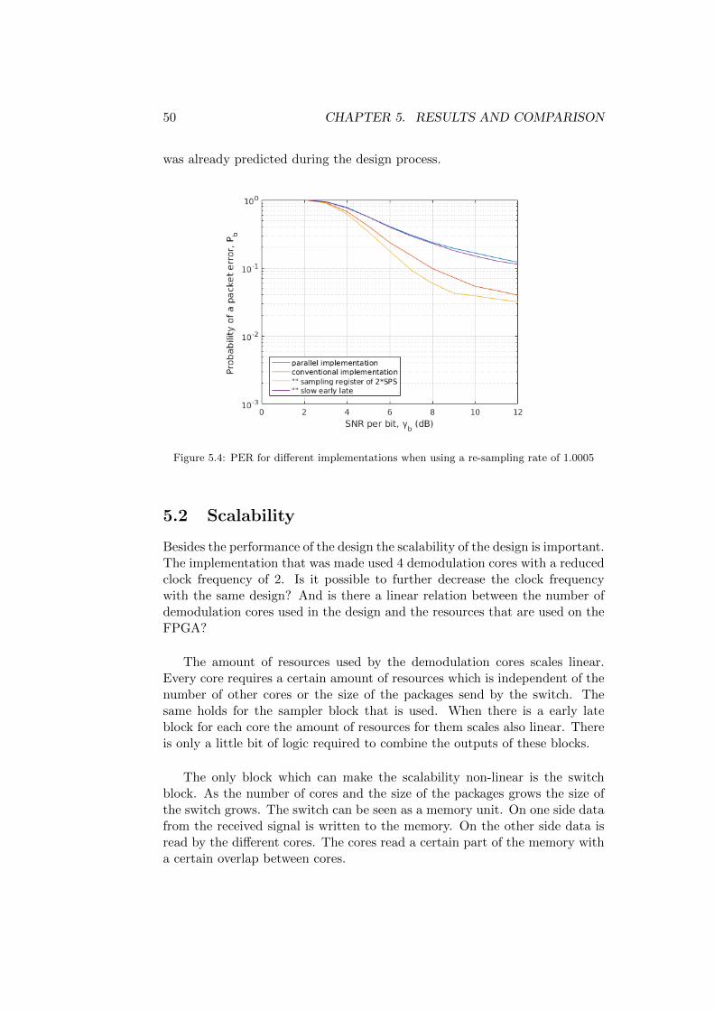
50 CHAPTER 5. RESULTS AND COMPARISON
was already predicted during the design process.
Figure 5.4: PER for different implementations when using a re-sampling rate of 1.0005
5.2 Scalability
Besides the performance of the design the scalability of the design is important.The implementation that was made used 4 demodulation cores with a reducedclock frequency of 2. Is it possible to further decrease the clock frequencywith the same design? And is there a linear relation between the number ofdemodulation cores used in the design and the resources that are used on theFPGA?
The amount of resources used by the demodulation cores scales linear.Every core requires a certain amount of resources which is independent of thenumber of other cores or the size of the packages send by the switch. Thesame holds for the sampler block that is used. When there is a early lateblock for each core the amount of resources for them scales also linear. Thereis only a little bit of logic required to combine the outputs of these blocks.
The only block which can make the scalability non-linear is the switchblock. As the number of cores and the size of the packages grows the size ofthe switch grows. The switch can be seen as a memory unit. On one side datafrom the received signal is written to the memory. On the other side data isread by the different cores. The cores read a certain part of the memory witha certain overlap between cores.
5.2. SCALABILITY 51
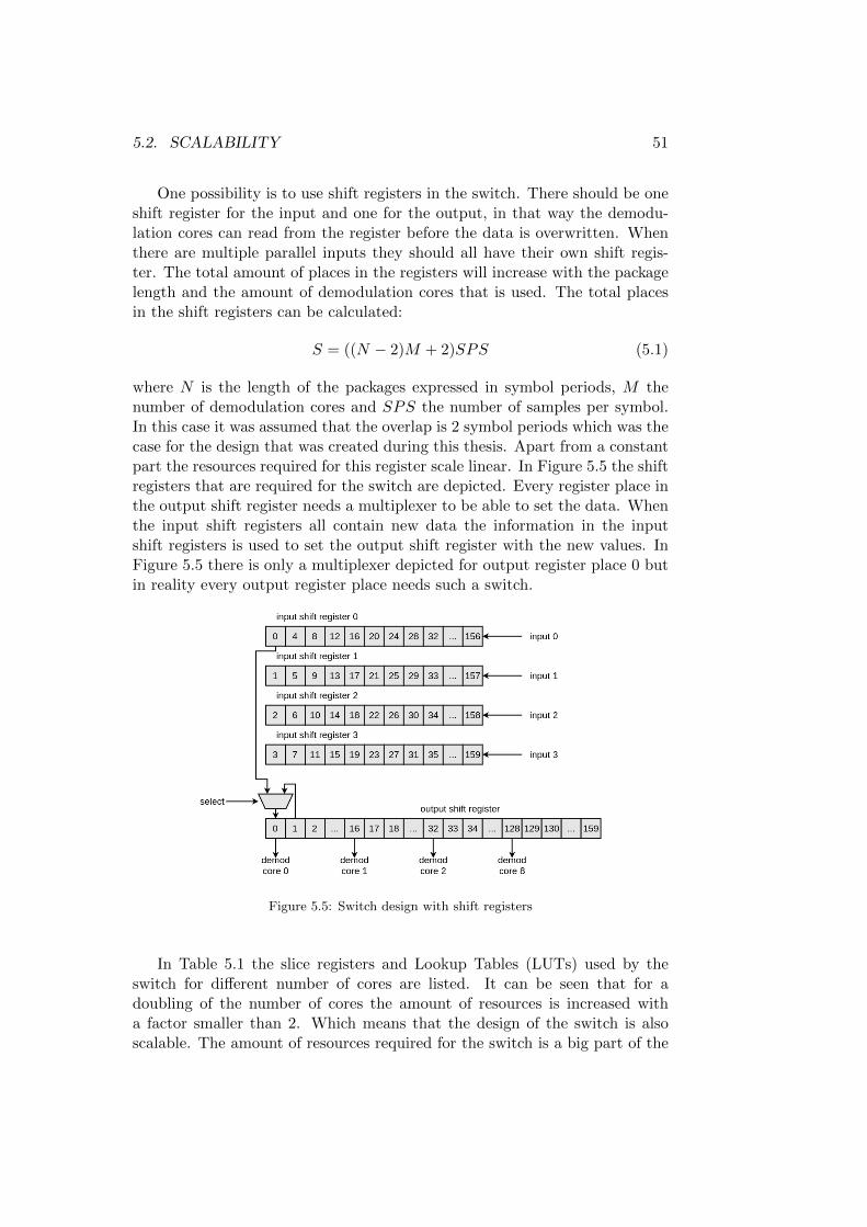
One possibility is to use shift registers in the switch. There should be oneshift register for the input and one for the output, in that way the demodu-lation cores can read from the register before the data is overwritten. Whenthere are multiple parallel inputs they should all have their own shift regis-ter. The total amount of places in the registers will increase with the packagelength and the amount of demodulation cores that is used. The total placesin the shift registers can be calculated:
S = ((N − 2)M + 2)SPS (5.1)
where N is the length of the packages expressed in symbol periods, M thenumber of demodulation cores and SPS the number of samples per symbol.In this case it was assumed that the overlap is 2 symbol periods which was thecase for the design that was created during this thesis. Apart from a constantpart the resources required for this register scale linear. In Figure 5.5 the shiftregisters that are required for the switch are depicted. Every register place inthe output shift register needs a multiplexer to be able to set the data. Whenthe input shift registers all contain new data the information in the inputshift registers is used to set the output shift register with the new values. InFigure 5.5 there is only a multiplexer depicted for output register place 0 butin reality every output register place needs such a switch.
Figure 5.5: Switch design with shift registers
In Table 5.1 the slice registers and Lookup Tables (LUTs) used by theswitch for different number of cores are listed. It can be seen that for adoubling of the number of cores the amount of resources is increased witha factor smaller than 2. Which means that the design of the switch is alsoscalable. The amount of resources required for the switch is a big part of the
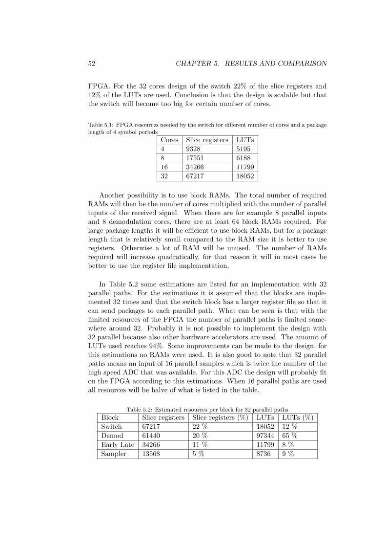
52 CHAPTER 5. RESULTS AND COMPARISON
FPGA. For the 32 cores design of the switch 22% of the slice registers and12% of the LUTs are used. Conclusion is that the design is scalable but thatthe switch will become too big for certain number of cores.
Table 5.1: FPGA resources needed by the switch for different number of cores and a packagelength of 4 symbol periods
Cores Slice registers LUTs
4 9328 5195
8 17551 6188
16 34266 11799
32 67217 18052
Another possibility is to use block RAMs. The total number of requiredRAMs will then be the number of cores multiplied with the number of parallelinputs of the received signal. When there are for example 8 parallel inputsand 8 demodulation cores, there are at least 64 block RAMs required. Forlarge package lengths it will be efficient to use block RAMs, but for a packagelength that is relatively small compared to the RAM size it is better to useregisters. Otherwise a lot of RAM will be unused. The number of RAMsrequired will increase quadratically, for that reason it will in most cases bebetter to use the register file implementation.
In Table 5.2 some estimations are listed for an implementation with 32parallel paths. For the estimations it is assumed that the blocks are imple-mented 32 times and that the switch block has a larger register file so that itcan send packages to each parallel path. What can be seen is that with thelimited resources of the FPGA the number of parallel paths is limited some-where around 32. Probably it is not possible to implement the design with32 parallel because also other hardware accelerators are used. The amount ofLUTs used reaches 94%. Some improvements can be made to the design, forthis estimations no RAMs were used. It is also good to note that 32 parallelpaths means an input of 16 parallel samples which is twice the number of thehigh speed ADC that was available. For this ADC the design will probably fiton the FPGA according to this estimations. When 16 parallel paths are usedall resources will be halve of what is listed in the table.
Table 5.2: Estimated resources per block for 32 parallel paths
Block Slice registers Slice registers (%) LUTs LUTs (%)
Switch 67217 22 % 18052 12 %
Demod 61440 20 % 97344 65 %
Early Late 34266 11 % 11799 8 %
Sampler 13568 5 % 8736 9 %
5.3. ALTERNATIVE PARALLEL STRUCTURE 53
5.3 Alternative Parallel Structure
Because the hardware resources that are required by the parallel design isincreasing fast for multiple cores a better structure is desirable. In Figure 5.6an alternative parallel design is depicted. In this case four parallel paths areused, which means that the clock frequency is reduced with a factor of four.In Figure 5.6 seven parallel inputs are depicted, these inputs are actually fourparallel inputs and three delayed inputs that are used for the filtering. Delayelements should therefore be added to the design.
In the demodulator each sample is multiplied with a different value of thecosine. In the alternative structure these multiplications are done in parallel.The results of these multiplications are filtered by a parallel FIR. This FIRfilter sums the samples that arrive in parallel and outputs the result to theoutput. Another FIR filter performs the filtering with another selection of theinput signals. When there are 4 parallel paths then there are also four parallelFIR filters in the structure. Each filtered signal is forwarded to a differentialmultiplier. The early late sampler determines which of the four samples is thesample that should be used.
This design does not require a switch for switching samples to the multiplecores which will reduce the amount of resources that are required. Anotherbenefit is that there is no invalid data at the outputs and therefore no resourcesare spilled on invalid data. Due to a lack of time this structure has not beenworked out in more detail. In future work this structure can be used to createa parallel structure that uses less resources.
5.4 Summary
In this chapter measurement results with the parallel implementation of thedemodulator were presented. These results were compared with the conven-tional implementation. The results of the PER measurements were worse thanthe conventional implementation, however some improvements were discussedwhich could improve the design. When the design was compared with anadapted version of the conventional design the results are almost identically.The scalability of the design was discussed and the conclusion is that the de-sign is scalable. However there will be too few resources on the FPGA whenthere are too many multiple paths. For the ADC this will most likely work butfor future designs some optimisations should be made for the parallel design.The main goal of this thesis was to develop a parallel demodulation structurein FPGA hardware, which has been presented in this chapter.
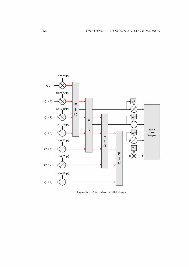
54 CHAPTER 5. RESULTS AND COMPARISON
Figure 5.6: Alternative parallel design
CHAPTER 6Conclusion and
Recommendations
55
56 CHAPTER 6. CONCLUSION AND RECOMMENDATIONS
This thesis discusses the implementation of a parallel demodulator on aFPGA. The demodulator was compared with a conventional implementationwhich processes the data sequential.
6.1 Conclusion
The first demodulator that was implemented was a conventional demodulator.This demodulator was compared with a demodulator that was made in GNU-Radio. The implementation that was made on the FPGA has for low SNRsthe same performance as the GNURadio implementation. For high SNRs theFPGA implementation has a certain floor, therefore it will never reach a PERof 0 %. Shortcomings of the design were discussed with relation to the sam-ple moment. When the sample moment is reset a bit loss will occur. Withextra hardware this could be prevented. It was chosen not to implement thisimprovement due to a lack of time. The design that was created formed thebasis of the parallel design.
After the conventional demodulator was implemented a parallel demod-ulator has been implemented. The design of it and its shortcomings werediscussed. The sampling register that was chosen to implement was actuallytoo small. It was chosen to implement only one symbol time recovery circuit,however from a PER performance perspective it was better to implement onefor each parallel path.
Measurements were done to compare the parallel implementation with theconventional one. From the measurements it was concluded that the parallelimplementation performs worse than the conventional one, however the resultslook promising. With some improvements that are discussed in this thesis thedesign should perform the same as the conventional design. However when theclock difference between the two becomes too high the parallel design will per-form worse. The main goal of this thesis, namely designing and implementinga parallel demodulation structure, is achieved.
The design that was presented can be scaled so that different numbers ofparallel paths are used. In that way it can be used for different bit-rates andinterfaced with ADCs running at higher clock frequencies. However, a lot ofresources are used when everything is implemented multiple times. The num-ber of parallel paths is limited by the amount of resources that are availableon the used FPGA. For the design that was presented the number of parallelpaths is limited to approximately 16.
Although the clock frequency of an FPGA does not keep up with thedata rate required by nowadays applications they can still be useful. It has
6.2. RECOMMENDATIONS 57
been shown that it is possible to create a scalable parallel demodulator onan FPGA. These parallel demodulators can be used in combination with highspeed ADCs which deliver samples in parallel. In that way it is possible toprocess the data from the 5GS/s ADC on the FPGA. The parallel structurepresented in this thesis can be used in the future to create other paralleldemodulation structures.
6.2 Recommendations
The main achievement in this thesis was to create a parallel structure for ademodulator. In this report a few improvements were discussed which prob-ably will improve the performance a lot. In future work this improvementscan be applied to the design and the performance can be tested. Another im-provement would be to implement the structure depicted in Figure 3.13. Thisstructure uses less hardware than the implementation that was made duringthis thesis.
Besides that it is also interesting to look at a frequency-domain paralleldemodulator. The design that was discussed in this report was based on atime-domain parallel demodulator. It would be interesting to compare thedesigns with each other. There can also be made improvements in the struc-ture that was presented. Afterwards splitting the input signal in packages wasprobably not the best solution to create a parallel demodulator. Because theswitch that is required will use a lot of space, besides that the demodulatorblock will take up a lot of space. For future work it could be interesting to in-vestigate other parallel designs principles that can be used for demodulation,for example the one presented in Section 5.3.
In this thesis there was no actual theoretical value for the PER used. Itwould be derive a theoretical upper bound on the PER for DBPSK. It isinteresting to know how good the design is according to this theory.
Due to timing constraints it was chosen not to use the high speed ADCthat was available. It would be interesting to interface the design with thisADC. In that way the performance of the system can be tested as it would bein a real high bit-rate receiver application.

List of Figures
2.1 Constellation Diagram of BPSK . . . . . . . . . . . . . . . . . . . 7
2.2 Probability of a symbol error for BPSK and DBPSK . . . . . . . . 7
2.3 Signal modulated using DBPSK (above) and bits that were used(below) . . . . . . . . . . . . . . . . . . . . . . . . . . . . . . . . . 9
2.4 Frequency response of two possible BPSK signals with 16 samplesper symbol . . . . . . . . . . . . . . . . . . . . . . . . . . . . . . . 9
2.5 Signals showing the bits that are modulated (a), modulated DBPSKsignal (b), I component (c) and Q component (d) of the signal aftermixing . . . . . . . . . . . . . . . . . . . . . . . . . . . . . . . . . . 12
2.6 Signals showing respectively the filtered I and Q component of thesignal, differential I and Q signal and the sum of both differentialsignals. . . . . . . . . . . . . . . . . . . . . . . . . . . . . . . . . . 13
3.1 Schematic of demodulation block . . . . . . . . . . . . . . . . . . . 18
3.2 Schematic of demodulation block . . . . . . . . . . . . . . . . . . . 18
3.3 Scheme of the sampling shift register (sample moment = 0, SPS =8) . . . . . . . . . . . . . . . . . . . . . . . . . . . . . . . . . . . . 19
3.4 Scheme of the sampling shift register (sample moment = 7, SPS =8) . . . . . . . . . . . . . . . . . . . . . . . . . . . . . . . . . . . . 19
3.5 Scheme of the sampling shift register with arrows indicating howthe sample moment can change in time . . . . . . . . . . . . . . . 20
3.6 Plot of the signal with the sample moments (arrows) that are used 20
3.7 Plot of the signal with the sample moments (arrows) that are used 21
3.8 Scheme of the bigger sampling shift register with arrows indicatinghow the sample moment can change in time . . . . . . . . . . . . . 22
3.9 Plot of the unfiltered signal with the sample moments (arrows)that are used, the circle indicates a local maximum that is not asymbol . . . . . . . . . . . . . . . . . . . . . . . . . . . . . . . . . . 22
3.10 Plot of the filtered signal with the sample moments (arrows) thatare used . . . . . . . . . . . . . . . . . . . . . . . . . . . . . . . . . 23
3.11 Eye diagram of the filtered signal . . . . . . . . . . . . . . . . . . . 23
3.12 Eye diagram of the unfiltered signal . . . . . . . . . . . . . . . . . 23
3.13 Schematic of the top level design demodulator using four mixers . 24
59
60 List of Figures
3.14 Schematic of the top level design demodulator including early latesampler . . . . . . . . . . . . . . . . . . . . . . . . . . . . . . . . . 24
3.15 Demodulator design in GNURadio . . . . . . . . . . . . . . . . . . 25
3.16 Higher order demodulator block design in GNURadio . . . . . . . 26
3.17 Complete signal flow graph at the receiver side . . . . . . . . . . . 26
3.18 Flow graph of the hardware accelerators that are used . . . . . . . 27
3.19 Schematic of the demod block (in red the Xilinx modules) . . . . . 27
3.20 Schematic of the early late block (in red the Xilinx modules) . . . 28
3.21 Schematic of the complete demodulation block (in red the Xilinxmodules) . . . . . . . . . . . . . . . . . . . . . . . . . . . . . . . . 28
3.22 Schematic of the setup that is used to perform the measurements . 29
3.23 Flow graph that was used in GNURadio to create test signals . . . 30
3.24 PER for the FPGA implementation, GNURadio implementationand the theoretical value assuming no error dependency . . . . . . 31
3.25 Exact sample moment and detected packages over time (SNR perbit = 10 dB) . . . . . . . . . . . . . . . . . . . . . . . . . . . . . . 32
3.26 PER of FPGA implementation for different re-sampling factors . . 33
3.27 Exact sample moment and detected packages over time for a re-sampling factor of 1.00001 (SNR per bit = 10 dB) . . . . . . . . . 33
3.28 PER of FPGA implementation for different re-sampling factorswith compensation for packet loss due to resets . . . . . . . . . . . 34
3.29 Effect of a sampling register that is exactly the length of the symbolperiod . . . . . . . . . . . . . . . . . . . . . . . . . . . . . . . . . . 35
3.30 PER for FPGA implementation with a sample register that is ex-actly the length of the symbol period with different re-samplingfactors. For comparison the PER of the FPGA implementationwith a sample register with a length of twice the symbol period isdepicted. . . . . . . . . . . . . . . . . . . . . . . . . . . . . . . . . 35
4.1 Illustration of the functioning of the switch . . . . . . . . . . . . . 39
4.2 Illustration of the functioning of the switch when the samples ar-rival in parallel . . . . . . . . . . . . . . . . . . . . . . . . . . . . . 39
4.3 Parallel demodulation . . . . . . . . . . . . . . . . . . . . . . . . . 40
4.4 Example of the best sample moment within a sampling registerwith a width of twice the symbol period . . . . . . . . . . . . . . . 41
4.5 Two examples of the best sample moment of a sampling registerwith a width equal to the symbol period . . . . . . . . . . . . . . . 42
4.6 Parallel demodulation . . . . . . . . . . . . . . . . . . . . . . . . . 43
4.7 Illustration of the functioning of the switch block . . . . . . . . . . 44
4.8 Demodulation block used in the parallel implementation . . . . . . 44
4.9 Parallel implementation . . . . . . . . . . . . . . . . . . . . . . . . 45
List of Figures 61
5.1 PER of parallel implementation for different re-sampling factors,for comparison the PER of the conventional implementation inGNURadio is also depicted. . . . . . . . . . . . . . . . . . . . . . . 48
5.2 PER for different implementations . . . . . . . . . . . . . . . . . . 495.3 Sample moment and total number of detected packages over time
for the parallel implementation . . . . . . . . . . . . . . . . . . . . 495.4 PER for different implementations when using a re-sampling rate
of 1.0005 . . . . . . . . . . . . . . . . . . . . . . . . . . . . . . . . . 505.5 Switch design with shift registers . . . . . . . . . . . . . . . . . . . 515.6 Alternative parallel design . . . . . . . . . . . . . . . . . . . . . . . 54

Bibliography
[1] 4DSP. FMC125 high pin count FMC ADC, 2015.
[2] Jan Crols and Michiel S. J. Steyaert. Low-IF topologies for high-performance analog front ends of fully integrated receivers. In IEEE trans-actions on circuits and systems II, March 1998.
[3] F.M. Gardner. A BPSK/QPSK timing error detector for sampled re-ceivers. In IEEE transactions on communications, May 1986.
[4] Changxing Lin, Beibei Shao, and Jian Zhang. A high data rate paralleldemodulator suited to FPGA implementation. In international symposiumon intelligent signal processing and communication systems, December2010.
[5] Louis Litwin. Matched filtering and timing recovery in digital receivers,September 2001. Online.
[6] K.H. Mueller and M. Muller. Timing recovery in digital synchronous datareceivers. In IEEE transactions on communications, May 1976.
[7] Martin Oerder and Heinrich Meyr. Digital filter and square timing recov-ery. In IEEE transactions on communications, May 1988.
[8] J.G. Proakis and M. Salehi. Digital communications, 4th edition (p. 274-278), 2000.
[9] Donald Rasmussen and George Davis. Serial and parallel demodulationtrade-offs for QBL-MSK. In tactical communications conference, May1994.
[10] Ettus Research. USRPTM N200/N210 networked series datasheet, 2012.
[11] James A. Roberts. Packet error rates for DPSK and differentially en-coded coherent BPSK. In IEEE transactions on communications, Febru-ary 1994.
[12] Epiq Solutions. Bitshark FMC-1RX broadband configurable RF receiver,2010.
63
64 BIBLIOGRAPHY
[13] M. Srinivasan, C.C. Chen, G. Grebowsky, and A. Gray. An all-digital,high data-rate parallel receiver. In international conference on signal pro-cessing applications and technology, 1997.
[14] Xilinx. IP LogiCORE FIR compiler v5.0, 2011.
[15] Xilinx. LogiCORE IP adder/subtracter v11.0, 2011.
[16] Xilinx. LogiCORE IP multiplier v11.2, 2011.
[17] Xilinx. LogiCORE IP RAM-based shift register v11.0, 2011.
[18] Xilinx. LogiCORE IP block memory generator v7.3, 2012.
[19] Xilinx. ML605 hardware user guide, 2012.
[20] Ronghua Zhou and Shuanghuan Li. A low complexity frequency-domainparallel demodulation structure combining matched filter with timing syn-chronization. In information and communications technologies, April2013.
Related Documents